EP3554066B1 - Festkörperbildgebungsvorrichtung - Google Patents
Festkörperbildgebungsvorrichtung Download PDFInfo
- Publication number
- EP3554066B1 EP3554066B1 EP19176172.5A EP19176172A EP3554066B1 EP 3554066 B1 EP3554066 B1 EP 3554066B1 EP 19176172 A EP19176172 A EP 19176172A EP 3554066 B1 EP3554066 B1 EP 3554066B1
- Authority
- EP
- European Patent Office
- Prior art keywords
- row selection
- shift register
- row
- signal
- state imaging
- Prior art date
- Legal status (The legal status is an assumption and is not a legal conclusion. Google has not performed a legal analysis and makes no representation as to the accuracy of the status listed.)
- Active
Links
Images






Classifications
-
- H—ELECTRICITY
- H04—ELECTRIC COMMUNICATION TECHNIQUE
- H04N—PICTORIAL COMMUNICATION, e.g. TELEVISION
- H04N25/00—Circuitry of solid-state image sensors [SSIS]; Control thereof
- H04N25/70—SSIS architectures; Circuits associated therewith
- H04N25/76—Addressed sensors, e.g. MOS or CMOS sensors
- H04N25/77—Pixel circuitry, e.g. memories, A/D converters, pixel amplifiers, shared circuits or shared components
- H04N25/778—Pixel circuitry, e.g. memories, A/D converters, pixel amplifiers, shared circuits or shared components comprising amplifiers shared between a plurality of pixels, i.e. at least one part of the amplifier must be on the sensor array itself
-
- H—ELECTRICITY
- H04—ELECTRIC COMMUNICATION TECHNIQUE
- H04N—PICTORIAL COMMUNICATION, e.g. TELEVISION
- H04N25/00—Circuitry of solid-state image sensors [SSIS]; Control thereof
- H04N25/60—Noise processing, e.g. detecting, correcting, reducing or removing noise
- H04N25/68—Noise processing, e.g. detecting, correcting, reducing or removing noise applied to defects
-
- H—ELECTRICITY
- H04—ELECTRIC COMMUNICATION TECHNIQUE
- H04N—PICTORIAL COMMUNICATION, e.g. TELEVISION
- H04N25/00—Circuitry of solid-state image sensors [SSIS]; Control thereof
- H04N25/70—SSIS architectures; Circuits associated therewith
- H04N25/76—Addressed sensors, e.g. MOS or CMOS sensors
- H04N25/767—Horizontal readout lines, multiplexers or registers
-
- H—ELECTRICITY
- H04—ELECTRIC COMMUNICATION TECHNIQUE
- H04N—PICTORIAL COMMUNICATION, e.g. TELEVISION
- H04N25/00—Circuitry of solid-state image sensors [SSIS]; Control thereof
- H04N25/70—SSIS architectures; Circuits associated therewith
- H04N25/76—Addressed sensors, e.g. MOS or CMOS sensors
- H04N25/779—Circuitry for scanning or addressing the pixel array
-
- H—ELECTRICITY
- H10—SEMICONDUCTOR DEVICES; ELECTRIC SOLID-STATE DEVICES NOT OTHERWISE PROVIDED FOR
- H10F—INORGANIC SEMICONDUCTOR DEVICES SENSITIVE TO INFRARED RADIATION, LIGHT, ELECTROMAGNETIC RADIATION OF SHORTER WAVELENGTH OR CORPUSCULAR RADIATION
- H10F39/00—Integrated devices, or assemblies of multiple devices, comprising at least one element covered by group H10F30/00, e.g. radiation detectors comprising photodiode arrays
- H10F39/80—Constructional details of image sensors
- H10F39/802—Geometry or disposition of elements in pixels, e.g. address-lines or gate electrodes
-
- H—ELECTRICITY
- H10—SEMICONDUCTOR DEVICES; ELECTRIC SOLID-STATE DEVICES NOT OTHERWISE PROVIDED FOR
- H10F—INORGANIC SEMICONDUCTOR DEVICES SENSITIVE TO INFRARED RADIATION, LIGHT, ELECTROMAGNETIC RADIATION OF SHORTER WAVELENGTH OR CORPUSCULAR RADIATION
- H10F39/00—Integrated devices, or assemblies of multiple devices, comprising at least one element covered by group H10F30/00, e.g. radiation detectors comprising photodiode arrays
- H10F39/10—Integrated devices
- H10F39/12—Image sensors
- H10F39/18—Complementary metal-oxide-semiconductor [CMOS] image sensors; Photodiode array image sensors
-
- H—ELECTRICITY
- H10—SEMICONDUCTOR DEVICES; ELECTRIC SOLID-STATE DEVICES NOT OTHERWISE PROVIDED FOR
- H10F—INORGANIC SEMICONDUCTOR DEVICES SENSITIVE TO INFRARED RADIATION, LIGHT, ELECTROMAGNETIC RADIATION OF SHORTER WAVELENGTH OR CORPUSCULAR RADIATION
- H10F39/00—Integrated devices, or assemblies of multiple devices, comprising at least one element covered by group H10F30/00, e.g. radiation detectors comprising photodiode arrays
- H10F39/10—Integrated devices
- H10F39/12—Image sensors
- H10F39/18—Complementary metal-oxide-semiconductor [CMOS] image sensors; Photodiode array image sensors
- H10F39/189—X-ray, gamma-ray or corpuscular radiation imagers
- H10F39/1898—Indirect radiation image sensors, e.g. using luminescent members
Definitions
- the present invention relates to a solid-state imaging device.
- Patent Literature 1 describes a technique concerning a radiation imaging device.
- the device comprises a sensor array constructed by two-dimensionally arraying a plurality of pixels each including a conversion element for converting a radiation from an object into an electric signal and a transfer switch for transferring the electric signal to the outside.
- the device also comprises a plurality of gate lines connecting the pixels of the sensor array in the row direction, a gate drive device for driving the gate lines in order to read out the electric signals of the pixels connected to each gate line, a plurality of signal lines for connecting the pixels of the sensor array in the column direction, and a plurality of amplifiers, provided so as to correspond to the respective signal lines, for amplifying and reading out the electric signals transferred from the respective transfer switches.
- Patent Literature 1 Japanese Patent Application Laid-Open No. 2007-50053
- US 2005/051774 A1 relates to a pixel structure comprising at least two selection switches coupled in series to improve the yield of the pixel.
- An array comprising such pixel structures logically organised in rows and columns is also described, as well as a method for selecting a row or column of pixel structures in such an array.
- US2007/216788 A1 relates to A CMOS-based sensor apparatus comprising an array of sensor cells that are interconnected by a first set of vertical driver lines to a selective driver facility and by a second set of horizontal sensing lines to a sensing facility for sensing respectively sensed amounts of radiation.
- a solid-state imaging device has a photodetecting section in which a plurality of pixels are arrayed two-dimensionally over a plurality of rows and a plurality of columns.
- a photodiode for converting light incident thereon into an electron is arranged in each pixel.
- the photodiodes of the pixels are connected through switch circuits (e.g., transistors) to a readout line provided for each column, while charges accumulated within the photodiode flow out to the readout line when the switch circuit is turned on.
- the charges reach an integration circuit through the readout line and are converted into a voltage signal in the integration circuit.
- a control terminal e.g., gate terminal
- a signal (row selection signal) from a shift register is supplied to the control terminal of each switch circuit through the row selection line, whereby the charges are read out from the pixels for each row.
- an operation of reading out the charges from each pixel also serves as a reset operation for getting ready for accumulating charges in the next frame.
- the row selection signal fails to reach pixels beyond the point of failure, whereby the switch circuit does not operate.
- the charges of the pixel keep accumulating in the photodiode and spill over pixels of other rows adjacent to the original row. This causes abnormality not only in the row in which a failure occurs in the row selection line, but also in other rows adjacent thereto. If abnormal output is generated in only one row by a failure of the row selection line, the output value of this row can be interpolated by pixel values of the rows adjacent thereto. When abnormal output occurs in a plurality of adjacent rows as described above, however, it becomes difficult to interpolate the output values of these rows.
- shift registers may be provided at both ends of the row selection line. Even when a disconnection occurs at a certain point in the row selection line, such a configuration can supply the row selection signal from both sides of the point of failure, so as to enable the switch circuit of each pixel to operate favorably.
- modes of failure of the row selection line include short circuits to nearby lines in addition to the disconnection. In the case where the row selection line short-circuits to a nearby line at a certain point, the row selection line (in the vicinity of the point where the short circuit occurs) fails to attain a predetermined potential even when supplied with the row selection signal from the shift registers, so that the switch circuit cannot operate, whereby the charges keep accumulating in the photodiode. Therefore, the above-described problem still remains.
- the solid-state imaging device in accordance with the present invention comprises a photodetecting section having M x N pixels (each of M and N being an integer of 2 or more), each including one photodiode and first and second switch 25 circuits each having one terminal connected to one terminal of the photodiode, two-dimensionally arrayed in M rows and N columns; N readout lines provided for the respective columns and connected to the other terminals of the first and second switch circuits included in the pixels of the corresponding columns; M first row selection lines provided for the respective rows and connected to control terminals of the first switch circuits included in the pixels of the corresponding rows; M first buffers having respective output terminals connected to the M first row selection lines; M second row selection lines provided for the respective rows and connected to control terminals of the second switch circuits included in the pixels of the corresponding rows; M second buffers having respective output terminals connected to the M second row selection lines; and a shift register section for generating a row selection signal for controlling an open/closed state of the
- each pixel is provided with two switch circuits (first switch circuit and second switch circuit). These switch circuits are connected in parallel with each other between one photodiode and a readout line. Therefore, charges accumulated in the photodiode flow out to the readout line through the two switch circuits.
- the control terminals of the two switch circuits are connected to the respective row selection lines (first row selection line and second row selection line) different from each other. Since the shift register section provides these row selection lines with a common row selection signal, the two switch circuits perform opening/closing operations at the same timing.
- the above-described solid-state imaging device can provide each pixel with a row selection signal through the other row selection line, thereby making it possible for at least one switch circuit to operate favorably. Therefore, even when the row selection line fails, the charges can be read out from each pixel and inhibited from spilling over pixels of the other rows.
- the above-described solid-state imaging device provides the first and second row selection lines with the respective buffers, even when one row selection line of the first and second row selection lines short-circuits to nearby lines, the other row selection line is not affected thereby and can transmit the row selection signal.
- the solid-state imaging device in accordance with the present invention can read out charges from each pixel even when a row selection line fails.
- Fig. 1 and Fig. 2 are diagrams illustrating a configuration of a solid-state imaging device 1A in this embodiment.
- Fig. 1 is a plan view illustrating the solid-state imaging device 1A
- Fig. 2 is a plan view enlarging a part of the solid-state imaging device 1A.
- Fig. 1 and Fig. 2 also depict an XYZ orthogonal coordinate system for easier understanding.
- the solid-state imaging device 1A comprises a photodetecting section 20, a readout circuit section 40, and a vertical shift register section 60A.
- the photodetecting section 20, readout circuit section 40, and vertical shift register section 60A are formed on a principal surface of a silicon substrate 12.
- the vertical shift register section 60A is juxtaposed with the photodetecting section 20 in the X-axis direction.
- the readout circuit section 40 includes a plurality of integration circuits provided so as to correspond to respective columns of the photodetecting section 20, while the integration circuits respectively generate voltage values corresponding to amounts of charges output from the pixels in the corresponding columns.
- the readout circuit section 40 holds the voltage values output from the respective integration circuits and sequentially outputs the held voltage values.
- the photodetecting section 20 is constructed by two-dimensionally arranging a plurality of pixels P 1,1 to P M,N over M rows and N columns (where each of M and N is an integer of 2 or more).
- Fig. 2 depicts six pixels P m,n-1 , P m,n , P m,n+1 , P m+1,n-1 , P m+1,n , and P m+1,n+1 as representative of the plurality of pixels P 1,1 to P M,N .
- the pixel P m,n is the one located on the m-th row and the n-th column (where m is an integer of 1 or more and M or less, and n is an integer of 1 or more and N or less).
- the column direction coincides with the Y-axis direction
- the row direction coincides with the X-axis directions.
- Each of the pixels P 1,1 to P M,N included in the photodetecting section 20 is constructed so as to include transistors 21, 22 and one photodiode 23.
- the transistors 21, 22 are first and second switch circuits, respectively, in this embodiment.
- the transistors 21, 22 are preferably constituted by field-effect transistors (FETs) but may also be constituted by bipolar transistors.
- FETs field-effect transistors
- the following explanation will assume the transistors 21 and 22 to be FETs. In this case, by control terminal is meant a gate.
- control terminal is meant a base.
- the photodiode 23 generates charges by an amount corresponding to the intensity of light incident thereon and accumulates thus generated charges in a junction capacitance part.
- the transistors 21, 22 have respective one terminals (e.g., their source regions) electrically connected to the photodiode 23.
- a scintillator which is not depicted, is disposed on the photodetecting section 20. The scintillator generates scintillation light according to X-rays incident thereon, converts an X-ray image into a light image, and outputs the light image to the photodiode 23.
- the solid-state imaging device 1A further comprises M first row selection lines QA 1 to QA M (represented by QA m and QA m+1 in Fig. 2 ) provided for the respective rows, M second row selection lines QB 1 to QB M (represented by QB m and QB m+1 in Fig. 2 ) provided for the respective rows, and a plurality of readout lines R 1 to R N (represented by R n-1 , R n , and R n+1 in Fig. 2 ).
- the first row selection line QA m at the m-th row electrically connects the control terminals (e.g., gate terminals) for controlling the open/closed state of the transistors 21 included in the pixels P m,1 to P m,N of the corresponding row to the vertical shift register section 60A.
- the second row selection line QB m at the m-th row electrically connects the control terminals (e.g., gate terminals) for controlling the open/closed state of the transistors 22 included in the pixels P m,1 to P m,N of the corresponding row to the vertical shift register section 60A.
- the vertical shift register section 60A generates a row selection signal for controlling the open/closed state of the transistors 21, 22 for each row and provides a common row selection signal for the row selection lines QA m , QB m at the m-th row.
- the readout line R n at the n-th column is electrically connected to the other terminals of the transistors 21, 22 (e.g., their drain regions) included in the pixels P 1,n to P M,n of the corresponding column.
- the row selection lines QA 1 to QA M , QB 1 to QB M and readout lines R 1 to R N are made of a metal, for example.
- Fig. 3 which is a side sectional view illustrating a cross section taken along the line I-I of Fig. 2 , depicts a cross-sectional structure of the photodetecting section 20 under magnification.
- a p-type well layer 14 is provided all over a principal surface of the silicon substrate 12.
- the p-type well layer 14 is formed by injecting p-type impurities into the principal surface of the silicon substrate 12, for example.
- the transistors 21, 22 and photodiode 23 are formed on the surface of the p-type well layer 14.
- the photodiode 23 is preferably constructed by a high-concentration n-type region 23a formed near a surface layer of the p-type well layer 14. That is, the photodiode 23 generates charges in the high-concentration n-type region 23a by an amount corresponding to the intensity of light incident thereon and accumulates the generated charges in a junction capacitance part between the high-concentration n-type region 23a and p-type well layer 14.
- the transistor 21 has a source region 21a and a drain region 21b which are made of a high-concentration n-type semiconductor.
- the source region 21a is formed integrally with the high-concentration n-type region 23a of the photodiode 23.
- a gate electrode 21c is provided on the p-type well layer 14 between the source region 21a and drain region 21b, while an insulating film 16 is interposed between the gate electrode 21c and p-type well layer 14.
- a branch part 27 of the readout line R 1 to R N is disposed on the drain region 21b of the transistor 21 with a metal conductor 24a and metal layers 25a, 25b interposed therebetween.
- the drain region 21b is electrically connected to the readout line R 1 to R N of its corresponding column through the metal conductor 24a, metal layers 25a, 25b, and branch part 27.
- the gate electrode 21c of the transistor 21 is electrically connected to the row selection line QA 1 to QA M of its corresponding row.
- Each of the row selection lines QA 1 to QA M which are disposed in regions between the pixels adjacent to each other, is placed on a pixel separation region 18 provided between the pixels adjacent to each other in this embodiment, for example.
- the pixel separation region 18 is made of a high-concentration p-type semiconductor, for example.
- a reference potential line 15 is provided in a layer between the row selection line QA 1 to QA M and the pixel separation region 18, while the reference potential line 15 is held at a reference potential (ground potential).
- the row selection line QA m and reference potential line 15 are arranged in this order as seen in the radiation incident direction.
- the reference potential line 15 and pixel separation region 18 are electrically connected to each other through a metal conductor 24b.
- the lateral width of the reference potential line 15 as seen in the thickness direction of the silicon substrate 12 is larger than the width of the row selection line QA 1 to QA M in the same direction.
- the transistor 22 has a source region 22a and a drain region 22b which are made of a high-concentration n-type semiconductor.
- the source region 22a is formed integrally with the high-concentration n-type region 23a of the photodiode 23.
- a gate electrode 22c is provided on the p-type well layer 14 between the source region 22a and drain region 22b, while the insulating film 16 is interposed between the gate electrode 22c and p-type well layer 14.
- a branch part 27 of the readout line R 1 to R N is disposed on the drain region 22b of the transistor 22 with a metal conductor 24a and metal layers 25a, 25b interposed therebetween.
- the drain region 22b is electrically connected to the readout line R 1 to R N of its corresponding column through the metal conductor 24a, metal layers 25a, 25b, and branch part 27.
- the gate electrode 22c of the transistor 22 is electrically connected to the row selection line QB 1 to QB M of its corresponding row.
- the row selection lines QB 1 to QB M are disposed on the pixels; for example, the row selection line QB m at the m-th row is disposed on the high-concentration n-type regions 23a of the photodiodes 23 included in the pixels P m,1 to P m,N of the corresponding row.
- a reference potential line 19 is provided in a layer between the row selection line QB 1 to QB M and the high-concentration n-type region 23a, while the reference potential line 19 is held at a reference potential (ground potential).
- the row selection line QB m and reference potential line 19 are arranged in this order as seen in the radiation incident direction.
- the lateral width of the reference potential line 19 as seen in the thickness direction of the silicon substrate 12 is larger than the width of the row selection line QB 1 to QB M in the same direction.
- a scintillator 13 is provided on the insulating layer 17 so as to cover the whole surface of the silicon substrate 12.
- the scintillator 13 generates scintillation light according to X-rays incident thereon, converts an X-ray image into a light image, and outputs the light image to the photodiodes 23.
- Fig. 4 is a diagram illustrating an inner configuration of the solid-state imaging device 1A.
- the solid-state imaging device 1A comprises M first buffers BA 1 to BA M having respective output terminals connected to the M first row selection lines QA 1 to QA M and M second buffers BB 1 to BB M having respective output terminals connected to the M second row selection lines QB 1 to QB M .
- the vertical shift register section 60A generates row selection signals VS 1 to VS M for controlling the open/closed state of the transistors 21, 22 (see Fig. 2 ) of the pixels P 1,1 to P M,N for the respective rows.
- the row selection signals VS 1 to VS M are common signals for the transistors 21, 22.
- the vertical shift register section 60A has M signal output terminals 62 provided one by one for the respective rows in order to output the row selection signals VS 1 to VS M , while the signal output terminals 62 are respectively connected to the input terminals of the buffers BA 1 to BA M and BB 1 to BB M at their corresponding rows.
- the vertical shift register section 60A provides the input terminals of the first buffer BA m and second buffer BB m with the row selection signal VS m for the m-th row.
- the first buffer BA m outputs a row selection signal VSA m based on the row selection signal VS m .
- the second buffer BB m outputs a row selection signal VSB m based on the row selection signal VS m .
- the row selection signals VS 1 to VS M sequentially become significant values in the vertical shift register section 60A.
- the readout circuit section 40 has N integration circuits 42 and N holding circuits 44 provided for the respective columns.
- the integration circuits 42 and holding circuits 44 are connected to each other in series for each column.
- the N integration circuits 42 have respective input terminals connected to the readout lines R 1 to R N , accumulate the charges input from the readout lines R 1 to R N , and output respective voltage values corresponding to the amounts of accumulated charges from their output terminals to the N holding circuits 44.
- the N integration circuits 42 are also connected to a reset line 46 provided in common for the N integration circuit 42.
- the N holding circuits 44 have respective input terminals connected to the output terminals of the integration circuits 42, hold the voltage values input to the input terminals, and output the held voltage values from the output terminals to a voltage output line 48.
- the N holding circuits 44 are connected to a hold line 45 provided in common for the N holding circuits 44.
- the N holding circuits 44 are also connected to a horizontal shift register section 61 through a first column selection line U 1 to an N-th column selection line U N .
- the horizontal shift register section 61 provides the N holding circuits 44 with column selection signals HS 1 to HS N through the column selection lines U 1 to U N , respectively.
- the column selection signals HS 1 to HS N sequentially become significant values.
- Each of the N integration circuits 42 is provided with a reset control signal RE through the reset line 46.
- Each of the N holding circuits 44 is provided with a hold control signal Hd through the hold line 45.
- Fig. 5 is a diagram illustrating a detailed circuit configuration example of the pixel P m,n , integration circuit 42, and holding circuit 44.
- a circuit diagram of the pixel P m,n on the m-th row and the n-th column is illustrated here.
- the photodiode 23 of the pixel P m,n has a grounded anode terminal and a cathode terminal connected to the readout line R n through the transistors 21, 22.
- the transistor 21 of the pixel P m,n is provided with the selection signal VSA m from the first buffer BA m through the first selection line QA m .
- the selection signal VSA m instructs the transistors 21 included in the N pixels P m,1 to P m,N of the m-th row to open/close.
- the transistor 22 of the pixel P m,n is provided with the selection signal VSB m from the second buffer BB m through the second selection line QB m .
- the selection signal VSB m instructs the transistors 22 included in the N pixels P m,1 to P m,N of the m-th row to open/close.
- the selection signals VSA m , VSB m are non-significant values (off-voltages for the control terminals of the transistors 21, 22)
- the charges generated in the photodiode 23 are accumulated in the junction capacitance part of the photodiode 23 without being output to the readout line R n .
- the selection signals VSA m , VSB m are significant values (on-voltages for the control terminals of the transistors 21, 22)
- the transistors 21, 22 are in a connected state. At this time, the charges accumulated in the junction capacitance part of the photodiode 23 are output to the readout line R n through the transistors 21, 22.
- the charges output from the photodiode 23 of the pixel P m,n are sent to the integration circuit 42 through the readout line R n . Since the selection signals VSA m , VSB m are generated from the common selection signal VS m , their non-significant value and significant value are switched at timings identical to each other.
- the integration circuit 42 has a so-called charge integration type configuration including an amplifier 42a, a capacitive element 42b, and a discharge switch 42c.
- the capacitive element 42b and discharge switch 42c are connected in parallel with each other between the input terminal and output terminal of the amplifier 42a.
- the amplifier 42a has an input terminal connected to the readout line R n .
- the discharge switch 42c is provided with the reset control signal RE through the reset line 46.
- the reset control signal RE instructs the respective discharge switches 42c of the N integration circuits 42 to open/close.
- the discharge switch 42c closes, so as to discharge the capacitive element 42b, thereby initializing the output voltage value of the integration circuit 42.
- the discharge switch 42c opens, so that the charges input to the integration circuit 42 are accumulated in the capacitive element 42b, whereby a voltage value corresponding to the amount of accumulated charges is output from the integration circuit 42.
- the holding circuit 44 includes an input switch 44a, an output switch 44b, and a capacitive element 44c. One end of the capacitive element 44c is grounded. The other end of the capacitive element 44c is connected to the output terminal of the integration circuit 42 through the input switch 44a and to the voltage output line 48 through the output switch 44b.
- the input switch 44a is provided with the hold control signal Hd through the hold line 45.
- the hold control signal Hd instructs the respective input switches 44a of the N holding circuits 44 to open/close.
- the output switch 44b of the holding circuit 44 is provided with the n-th column selection signal HS n through the n-th column selection line U n .
- the selection signal HS n instructs the output switch 44b of the holding circuit 44 to open/close.
- the input switch 44a changes from the closed state to the open state, whereupon the voltage value input to the holding circuit 44 is held by the capacitive element 44c.
- the output switch 44b is closed, whereupon the voltage value held by the capacitive element 44c is output to the voltage output line 48.
- Fig. 6 is a circuit diagram illustrating an inner configuration example of buffers BA m , BB m .
- the buffers BA m , BB m are impedance converters which output their input signals with low impedance and generate output signals (selection signals VSA m , VSB m ) corresponding to their received power supply voltage regardless of the magnitude of the input signal (selection signal VS m ).
- the buffers BA m , BB m illustrated in Fig. 6 include two-stage amplifier circuits B1, B2, each of which is constituted by a CMOS inverter.
- each of the amplifier circuits B1, B2 is constructed so as to include two MOSFETs (p-MOSFET 51 and n-MOSFET 52).
- the drain terminal of the p-MOSFET 51 and the drain terminal of the n-MOSFET 52 are connected to each other, the source terminal of the p-MOSFET 51 is connected to a positive power supply potential Vdd, and the source terminal of the n-MOSFET 52 is connected to a negative power supply potential Vss.
- the selection signal VS m is input to the gate terminals of the p-MOSFET 51 and n-MOSFET 52 in the amplifier circuit B1.
- the drain terminals of the p-MOSFET 51 and n-MOSFET 52 in the amplifier circuit B1 are connected to the gate terminals of the p-MOSFET 51 and n-MOSFET 52 in the amplifier circuit B2.
- a signal from the drain terminals of the p-MOSFET 51 and n-MOSFET 52 in the amplifier circuit B2 is output as the selection signal VSA m , VSB m .
- Both capacitance and resistance are large in the first row selection lines QA 1 to QA M and second row selection lines QB 1 to QB M . Therefore, for switching voltage values of the selection signals VSA m , VSB m within a predetermined time, it is desirable for the buffers BA m , BB m to be able to output large currents. Since CMOS inverters such as those described above have low output impedance, employing CMOS inverters in the amplifier circuits B1, B2 can favorably achieve the buffers BA m , BB m capable of outputting large currents.
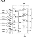
- Fig. 7 is a circuit diagram illustrating a detailed configuration of the vertical shift register section 60A in this embodiment. As illustrated in Fig. 7 , the vertical shift register section 60A has a shift register array 41 and M logic circuits LO 1 to LO M (represented by LO 1 to LO 4 in the diagram).
- the shift register array 41 is constructed by connecting M shift register circuits 43 in series.
- the shift register circuits 43 are arranged one by one for the respective rows.
- the shift register circuits 43 are constituted by a plurality of FETs having configurations similar to those of the transistors 21, 22 illustrated in Fig. 3 , for example.
- a clock line Lc is connected to the shift register circuits 43, whereby a clock signal clk having a fixed period is supplied from the clock line Lc to each shift register circuit 43.
- the M logic circuits LO 1 to LO M are arranged so as to correspond to the respective rows, while the output terminal of the logic circuit LO m at the m-th row is connected to the input terminals of the above-described buffers BA m , BB m through the signal output terminal 62 provided for each row.
- An enable line En is connected to respective one input terminals of the logic circuits LO 1 to LO M , whereby a control input signal enable is supplied from the enable line En to the logic circuits LO 1 to LO M .
- Connected to the respective other input terminals of the logic circuits LO 1 to LO M are output terminals of the shift register circuits 43 corresponding to their rows.
- the M logic circuits LO 1 to LO M output the respective row selection signals VS 1 to VS M so as to close the transistors 21, 22 when both of the control input signal enable and output signals Sout 1 to Sout M from their corresponding shift register circuits 43 are significant values.
- the logic circuit LO m at the m-th row outputs a logical conjunction (AND) of the control input signal enable and the output signal Sout m from the shift register circuit 43.
- the logic circuits LO 1 to LO M are illustrated by symbols representing AND circuits in Fig. 7 , but may be constructed by combinations of various other logic circuits.
- Fig. 8 is a timing chart illustrating operations of the vertical shift register section 60A in this embodiment.
- Fig. 8 illustrates, successively from the upper side, (a) start signal Start, (b) clock signal clk, (c) output signal Sout 1 from the shift register circuit 43 at the first row, (d) output signal Sout 2 from the shift register circuit 43 at the second row, (e) output signal Sout 3 from the shift register circuit 43 at the third row, (f) output signal Sout 4 from the shift register circuit 43 at the fourth row, (g) control input signal enable, (h) first row selection signal VSA 1 , (i) first row selection signal VSB 1 , (j) second row selection signal VSA 2 , (k) second row selection signal VSB 2 , (l) third row selection signal VSA 3 , (m) third row selection signal VSB 3 , (n) fourth row selection signal VSA 4 , and (o) fourth row selection signal VSB 4 .
- the start signal Start is set to the high level in a period from time t 10 to time t 13 .
- the output signal Sout 1 from the shift register circuit 43 at the first row rises (time t 11 ).
- the output signal Sout 1 falls as the next clock signal clk rises (time t 15 ).
- the control input signal enable is set to the high level during a predetermined period (time t 12 to t 14 ) included in the duration from time t 11 to time t 15 when the output signal Sout 1 is the high level. This causes the first row selection signals VSA 1 , VSB 1 to have the high levels, thereby turning on the transistors 21, 22 included in the respective pixels P 1,1 to P 1,N at the first row.
- the output signal Sout 2 from the shift register circuit 43 at the second row rises (time t 15 ).
- the output signal Sout 2 falls as the next clock signal clk rises (time t 18 ).
- the control input signal enable is set to the high level again during a predetermined period (time t 16 to t 17 ) included in the duration from time t 15 to time t 18 when the output signal Sout 2 is the high level.
- This causes the second row selection signals VSA 2 , VSB 2 to have the high levels, thereby turning on the transistors 21, 22 included in the respective pixels P 2,1 to P 2,N at the second row.
- operations similar to that at the second row cause the selection signals VSA m , VSB m at the third and later rows to become high levels in sequence, thereby successively turning on the transistors 21, 22 included in each pixel for the respective rows.
- Fig. 9 is a timing chart of respective signals.
- Fig. 9 illustrates, successively from the upper side, (a) reset control signal RE, (b) first row selection signal VSA 1 , (c) first row selection signal VSB 1 , (d) second row selection signal VSA 2 , (e) second row selection signal VSB 2 , (f) M-th row selection signal VSA M , (g) M-th row selection signal VSB M , (h) hold control signal Hd, and (i) first column selection signal HS 1 to N-th column selection signal HS N .
- the reset control signal RE is set to the high level during a period from time t 20 to time t 21 as illustrated in Fig. 9 . This closes the discharge switches 42c in the N integration circuits 42, thereby discharging the capacitive elements 42b.
- the operations illustrated in Fig. 8 set the first row selection signals VSA 1 , VSB 1 to the high levels. This turns the transistors 21, 22 into the connected states in the pixels P 1,1 to P 1,N at the first row, whereby the charges accumulated in the photodiodes 23 of the pixels P 1,1 to P 1,N are output to the integration circuits 42 throughout the readout lines R 1 to R N , so as to accumulate in the capacitive elements 42b. Each integration circuit 42 outputs a voltage value having a magnitude corresponding to the amount of charges accumulated in the capacitive element 42b. After time t 23 , the transistors 21, 22 in each of the pixels P 1,1 to P 1,N at the first row are turned into unconnected states.
- the hold control signal Hd is set to the high level, which turns the input switch 44a into the connected state in each of the N holding circuits 44, whereby the voltage value output from the integration circuit 42 is held by the capacitive element 44c.
- the horizontal shift register section 61 turns the first column selection signal HS 1 to N-th column selection signal HS N into the high levels in sequence. This successively closes the output switches 44b of the N holding circuits 44, whereby the voltage values held by the capacitive elements 44c are sequentially output to the voltage output line 48. During this period, the reset control signal RE is set to the high level, whereby the capacitive element 42b of each integration circuit 42 is discharged.
- the second row selection signals VSA 2 , VSB 2 are set to the high levels. This turns the transistors 21, 22 into connected states in the pixels P 2,1 to P 2,N at the second row, whereby the charges accumulated in the photodiodes 23 of the pixels P 2,1 to P 2,N are output to the integration circuits 42 through the readout lines R 1 to R N , so as to be accumulated in the capacitive elements 42b.
- an operation similar to that at the first row successively outputs the voltage values having magnitudes corresponding to the amounts of charges accumulated in the capacitive elements 42b from the N holding circuits 44 to the voltage output line 48.
- Operations similar to that at the first row also convert the charges accumulated in the pixels at the third to M-th rows into voltage values and successively output them to the voltage output line 48. This completes the readout of image data by one image frame from the photodetecting section 20.
- the operation of reading out charges from each of the pixels P 1,1 to P M,N also serves as a reset operation for getting ready for accumulating charges in the next frame.
- a failure such as short circuit occurs in a row selection line in a conventional solid-state imaging device, however, a row selection signal fails to reach pixels beyond the point of failure, whereby a switch circuit does not operate.
- the charges in the pixel keep accumulating in the photodiode and spill over pixels of other rows adjacent to the original row. This causes abnormality not only in the row in which a failure occurs in the row selection line, but also in other rows adjacent thereto.
- the solid-state imaging device has such a multilayer structure of metal lines as illustrated in Fig. 3 , i.e., a structure in which a first layer for forming a reference potential line, a second layer for forming a row selection line, and a third layer for forming a readout line are stacked, the reference potential line of the first layer and the row selection line of the second layer may short-circuit to each other.
- the solid-state imaging device 1A provides each of the pixels P 1,1 to P M,N with two switch circuits (transistors 21, 22).
- the transistors 21, 22 in each of the pixels P 1,n to P M,n at the n-th column are connected in parallel with each other between the photodiode 23 and the readout line R n . Therefore, the charges accumulated in the photodiode 23 flow out to the readout line R n through the transistors 21, 22.
- the control terminals of the transistors 21, 22 in the pixels P m,1 to P m,N at the m-th row are connected to the row selection lines QA m , QB m separate from each other.
- the row selection lines QA m , QB m are provided with the common row selection signals VSA m , VSB m , respectively, from the vertical shift register section 60A, whereby the transistors 21, 22 open/close at the same timing.
- the solid-state imaging device 1A can provide each of the pixels P m,1 to P m,N with the row selection signal VSA m or VSB m through the other row selection line, thereby making it possible for at least one of the transistors 21, 22 to operate favorably. Therefore, even when one of the row selection lines QA m , QB m fails, the charges can be read out from each of the pixels P m,1 to P m,N and effectively inhibited from spilling over pixels of the other rows adjacent thereto.
- the solid-state imaging device 1A of this embodiment provides the row selection lines QA m , QB m with the respective buffers BA m , BB m , even when one of the row selection lines QA m , QB m short-circuits to nearby lines, the other row selection line is not affected thereby and can transmit the row selection signal VSA m or VSB m .
- the probability of both the row selection lines QA m , QB m short-circuiting at the same time is so low that it is hardly problematic.
- the row selection lines QA m , QB m may be arranged such that one row selection line QA m is disposed in a region between the pixels while the other row selection line QB m is disposed on the pixels P m,1 to P m,N .
- This can place the row selection lines QA m , QB m such that they are separated from each other, thereby enhancing the yield at the time of manufacturing the solid-state imaging device 1A.
- This can also form the row selection lines QA m , QB m within the same layer unlike a fourth modified example which will be explained later.
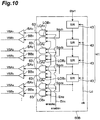
- Fig. 10 is a circuit diagram illustrating a detailed configuration of a vertical shift register section 60B as a first modified example of the above-described embodiment.
- the vertical shift register section 60B has a shift register array 41, M logic circuits LOA 1 to LOA M (represented by LOA 1 to LOA 4 in the diagram) and M logic circuits LOB 1 to LOB M (represented by LOB 1 to LOB 4 in the diagram).
- the shift register array 41 is constructed as in the above-described embodiment.
- the M logic circuits LOA 1 to LOA M are arranged so as to correspond to the respective rows, while the output terminal of the logic circuit LOA m at the m-th row is connected to the input terminal of the buffer BA m through one of two signal output terminals 63 provided for each row.
- the M logic circuits LOB 1 to LOB M are also arranged so as to correspond to the respective rows, while the output terminal of the logic circuit LOB m at the m-th row is connected to the input terminal of the buffer BB m through the other of the two signal output terminals 63 provided for each row.
- a first enable line En A is connected to one input terminal each of the logic circuits LOA 1 to LOA M , whereby a first control input signal enable 1 is supplied from the enable line En A to the logic circuits LOA 1 to LOA m .
- Connected to the other input terminals of the logic circuits LOA 1 to LOA M are output terminals of the shift register circuits 43 corresponding to their rows.
- a second enable line En B is connected to one input terminal each of the logic circuits LOB 1 to LOB M , whereby a second control input signal enable 2 is supplied from the enable line En B to the logic circuits LOB 1 to LOB M .
- Connected to the other input terminals of the logic circuits LOB 1 to LOB M are output terminals of the shift register circuits 43 corresponding to their rows.
- the logic circuits LOA 1 to LOA M output the respective row selection signals VSA 1 to VSA M so as to close the transistors 21 when both of the control input signal enable 1 and output signals Sout 1 to Sout M from their corresponding shift register circuits 43 are significant values.
- the logic circuits LOB 1 to LOB M output the respective row selection signals VSB 1 to VSB M so as to close the transistors 22 when both of the control input signal enable 2 and output signals Sout 1 to Sout M from their corresponding shift register circuits 43 are significant values.
- the logic circuits LOA 1 to LOA M and LOB 1 to LOB M are illustrated by symbols representing AND circuits in Fig. 10 , but may be constructed by combinations of various other logic circuits.
- the vertical shift register section 60B acts as with the vertical shift register section 60A illustrated in Fig. 8 .
- the above-described embodiment can employ the vertical shift register section 60B of this modified example in place of the vertical shift register section 60A. Effects similar to those of the above-described embodiment can favorably be exhibited in this case as well.
- Fig. 11 is a circuit diagram illustrating a configuration of a second modified example of the above-described embodiment. Unlike the above-described embodiment, each row is provided with one buffer in this modified example. Specifically, this solid-state imaging device comprises M buffers B 1 to B M having output terminals connected to both of M first row selection lines QA 1 to QA M and M second row selection lines QB 1 to QB M .
- the vertical shift register section 60A has M signal output terminals 62 provided one by one for the respective rows in order to output the row selection signals VS 1 to VS M , and the signal output terminals 62 are connected to the input terminals of the buffers B 1 to B M at their corresponding rows.
- the vertical shift register section 60A provides the input terminal of the buffer B m with the row selection signal VS m at the m-th row.
- the output signal from the buffer B m is supplied as row selection signals VSA m , VSB m to the row selection lines QA m , QB m .
- Fig. 12 is a circuit diagram illustrating a detailed configuration of a vertical shift register section 60C as a third modified example of the above-described embodiment.
- the vertical shift register section 60C of this modified example differs from the vertical shift register section 60B of the first modified example in the following points.
- the vertical shift register section 60C has a first shift register array 41A and a second shift register array 41B in place of the shift register array 41 in the first modified example.
- the shift register array 41A is constructed by connecting in series M shift register circuits 43 arranged one by one for the respective rows, while a clock line Lc 1 is connected to the shift register circuits 43, whereby each shift register circuit 43 is provided with a clock signal clk 1 having a fixed period from the clock line Lc 1 .
- the shift register array 41B is constructed by connecting in series M shift register circuits 43 arranged one by one for the respective rows, while a clock line Lc 2 is connected to the shift register circuits 43, whereby each shift register circuit 43 is provided with a clock signal clk 2 having a fixed period from the clock line Lc 2 .
- the clock signals clk 1 , clk 2 are clock signals having periods identical to each other and operate at the same timing.
- the first enable line En A is connected to one input terminal each of the logic circuits LOA 1 to LOA M , whereby the first control input signal enable 1 is supplied from the enable line En A to the logic circuits LOA 1 to LOA M .
- Connected to the other input terminals of the logic circuits LOA 1 to LOA M are output terminals of the shift register circuits 43 corresponding to their rows in the first shift register array 41A.
- the second enable line En B is connected to one input terminal each of the logic circuits LOB 1 to LOB M , whereby the second control input signal enable 2 is supplied from the enable line En B to the logic circuits LOB 1 to LOB M .
- Connected to the other input terminals of the logic circuits LOB 1 to LOB M are output terminals of the shift register circuits 43 corresponding to their rows in the second shift register array 41B.
- the logic circuits LOA 1 to LOA M output the respective row selection signals VSA 1 to VSA M so as to close the transistors 21 when both of the control input signal enable 1 and output signals SAout 1 to SAout M from their corresponding shift register circuits 43 are significant values.
- the logic circuits LOB 1 to LOB M output the respective row selection signals VSB 1 to VSB M so as to close the transistors 22 when both of the control input signal enable 2 and output signals SBout 1 to SBout M from their corresponding shift register circuits 43 are significant values.
- the vertical shift register section 60C acts as with the vertical shift register section 60A illustrated in Fig. 8 .
- the clock signals clk 1 , clk 2 it is desirable for the clock signals clk 1 , clk 2 to have a signal waveform identical to the signal waveform of the clock signal clk in (b) in Fig. 8 .
- the first and second control input signals enable 1 , enable 2 to have a signal waveform identical to the signal waveform of the control input signal enable in (g) in Fig. 8 .
- the above-described embodiment can employ the vertical shift register section 60C of this modified example in place of the vertical shift register section 60A. Effects similar to those of the above-described embodiment can favorably be exhibited in this case as well.
- Fig. 13 is a plan view illustrating a part of a photodetecting section under magnification as a fourth modified example of the above-described embodiment.
- this modified example differs from the above-described embodiment in that both of the row selection lines QA 1 to QA M and QB 1 to QB M are disposed in regions between pixels.
- the row selection lines QA m , QB m of m-th row are disposed between the pixels P m,1 to P m,N at the m-th row and the pixels P m+1,1 to P m+1,N at the (m+1)-th row.
- Such a configuration of this modified example can prevent the row selection lines QA 1 to QA M or QB 1 to QB M from obstructing light incident on the pixels P 1,1 to P M,N , thereby raising the efficiency at which light is incident on the pixels P 1,1 to P M,N . It can also keep the row selection lines QA 1 to QA M and QB 1 to QB M away from the photodiodes 23 of the pixels P 1,1 to P M,N , thereby suppressing the fluctuation of the amount of charges in the photodiodes 23 caused by the voltage change in the row selection lines QA 1 to QA M and QB 1 to QB M .
- the row selection lines QA 1 to QA M and the row selection lines QB 1 to QB M may be disposed in parallel with each other in the layer stacking direction.
- a wiring layer including the row selection lines QB 1 to QB M may be added onto a wiring layer including the row selection lines QA 1 to QA M . This can increase the gap between the row selection lines QB 1 to QB M and the reference potential line, thereby lowering the probability of the row selection lines QB 1 to QB M and the reference potential line short-circuiting to each other.
- the solid-state imaging device in accordance with the present invention is not limited to the above-described embodiment but can be modified in various ways.
- the photodetecting section illustrated in the above-described embodiment may comprise a configuration in which a film of polycrystalline silicon or amorphous silicon is formed on a glass substrate.
- the transistors 21, 22 are favorably constructed by thin-film transistors.
- the photodetecting section may also be made on a monocrystalline silicon substrate.
- the row selection signals VSA m , VSB m are input to two row selection lines QA m , QB m for the same row at the same timing in the above-described embodiment, but the row selection signals VSA m , VSB m may be input to two row selection lines QA m , QB m for the same row at the same timing only partly or at timings different from each other in the first modified example and the third modified example.
- a solid-state imaging device including all of the above-described embodiment and first to third modified examples has a configuration comprising:
- a solid-state imaging device including the above-described first and third modified examples has a configuration further comprising:
- a solid-state imaging device including the above-described second modified example has a configuration further comprising:
- the solid-state imaging device in accordance with the above-described embodiment uses a configuration comprising a photodetecting section having M x N pixels (each of M and N being an integer of 2 or more), each including one photodiode and first and second switch circuits each having one terminal connected to one terminal of the photodiode, two-dimensionally arrayed in M rows and N columns; N readout lines provided for the respective columns and connected to the other terminals of the first and second switch circuits included in the pixels of the corresponding columns; M first row selection lines provided for the respective rows and connected to control terminals of the first switch circuits included in the pixels of the corresponding rows; M first buffers having respective output terminals connected to the M first row selection lines; M second row selection lines provided for the respective rows and connected to control terminals of the second switch circuits included in the pixels of the corresponding rows; M second buffers having respective output terminals connected to the M second row selection lines; and a shift register section for generating a row selection signal for controlling an opening/closing state of the first and
- the solid-state imaging device may have a configuration in which the first and second row selection lines are disposed in a region between the pixels. This can prevent the row selection lines from obstructing light incident on each pixel, thereby enhancing the efficiency at which light is incident on each pixel. It can also keep the row selection lines away from the photodiodes of the pixels, thereby suppressing the fluctuation of the amount of charges in the photodiodes caused by the voltage change in the row selection lines.
- the solid-state imaging device may have a configuration in which one row selection line of the first and second row selection lines is disposed in a region between the pixels, while the other row selection line is disposed on the pixel. This can place the two row selection lines such that they are separated from each other, thereby enhancing the yield at the time of manufacturing the solid-state imaging device. In this case, for suppressing the fluctuation of the amount of charges in the photodiodes caused by the voltage fluctuation in the other row selection line, it will be more preferred if a reference potential line is disposed between the other row selection line and the pixel.
- the present invention can be utilized as a solid-state imaging device which can read charges from each pixel even when a row selection line fails.
Landscapes
- Engineering & Computer Science (AREA)
- Multimedia (AREA)
- Signal Processing (AREA)
- Solid State Image Pick-Up Elements (AREA)
- Transforming Light Signals Into Electric Signals (AREA)
- Apparatus For Radiation Diagnosis (AREA)
Claims (11)
- Festkörperbildgebungsvorrichtung (1A), umfassend:einen Photodetektionsabschnitt (20) mit M x N Pixeln, wobei jedes von M und N eine ganze Zahl von 2 oder mehr ist, die jeweils eine Photodiode (23) und erste und zweite Schaltkreise (21, 22) enthalten, die jeweils einen Anschluss aufweisen, der mit einem Anschluss der Photodiode (23) verbunden ist, zweidimensional in M Zeilen und N Spalten angeordnet;N Leseleitungen, die für die jeweiligen Spalten bereitgestellt sind und mit den anderen Anschlüssen der ersten und zweiten Schaltkreise (21, 22) verbunden sind, die in den Pixeln der entsprechenden Spalten enthalten sind;M erste Zeilenauswahlleitungen, die für die jeweiligen Zeilen bereitgestellt sind und mit Steueranschlüssen der ersten Schaltkreise verbunden sind, die in den Pixeln der entsprechenden Zeilen enthalten sind;M zweite Zeilenauswahlleitungen, die für die jeweiligen Zeilen bereitgestellt sind und mit Steueranschlüssen der zweiten Schaltkreise verbunden sind, die in den Pixeln der entsprechenden Zeilen enthalten sind; undeinen Schieberegisterabschnitt (60A), der konfiguriert ist, ein Zeilenauswahlsignal zum Steuern eines Offen-/Geschlossen-Zustands der ersten und zweiten Schaltkreise (21, 22) für jede Zeile zu erzeugen und das Zeilenauswahlsignal an erste und zweite Zeilenauswahlleitungen bereitzustellen.
- Festkörperbildgebungsvorrichtung (1A) nach Anspruch 1, weiter umfassend:M erste Puffer mit jeweiligen Ausgangsanschlüssen, die mit den M ersten Zeilenauswahlleitungen verbunden sind; undM zweite Puffer mit jeweiligen Ausgangsanschlüssen, die mit den M zweiten Zeilenauswahlleitungen verbunden sind.
- Festkörperbildgebungsvorrichtung (1A) nach Anspruch 2, wobei der Schieberegisterabschnitt (60A) weiter konfiguriert ist, das Zeilenauswahlsignal zu erzeugen und das gemeinsame Zeilenauswahlsignal an Eingangsanschlüsse der ersten und zweiten Puffer bereitzustellen.
- Festkörperbildgebungsvorrichtung (1A) nach Anspruch 2 oder 3, wobei der Schieberegisterabschnitt (60A) 2xM Signalausgangsanschlüsse aufweist, die paarweise für die entsprechenden Zeilen zum Ausgeben des Zeilenauswahlsignals bereitgestellt sind, wobei die Signalausgangsanschlüsse jeweils mit Eingangsanschlüssen der ersten und zweiten Puffer der entsprechenden Zeilen verbunden sind.
- Festkörperbildgebungsvorrichtung (1A) nach Anspruch 1, weiter umfassend:
M Puffer mit jeweiligen Ausgangsanschlüssen, die mit den M ersten Zeilenauswahlleitungen und den M zweiten Zeilenauswahlleitungen verbunden sind. - Festkörperbildgebungsvorrichtung (1A) nach Anspruch 5, wobei der Schieberegisterabschnitt (60A) M Signalausgangsanschlüsse aufweist, die einzeln für die entsprechenden Zeilen zum Ausgeben des Zeilenauswahlsignals bereitgestellt sind, wobei die Signalausgangsanschlüsse mit Eingangsanschlüssen der Puffer der entsprechenden Zeilen verbunden sind.
- Festkörperbildgebungsvorrichtung (1A) nach Anspruch 4, wobei der Schieberegisterabschnitt (60A) eine erste Schieberegisteranordnung und eine zweite Schieberegisteranordnung aufweist.
- Festkörperbildgebungsvorrichtung (1A) nach einem der Ansprüche 1 bis 6, wobei der Schieberegisterabschnitt (60A) eine Schieberegisteranordnung aufweist.
- Festkörperbildgebungsvorrichtung (1A) nach einem der Ansprüche 1 bis 8, wobei die ersten und zweiten Zeilenauswahlleitungen in einem Bereich zwischen den Pixeln angeordnet sind.
- Festkörperbildgebungsvorrichtung (1A) nach einem der Ansprüche 1 bis 8, wobei eine Zeilenauswahlleitung der ersten und zweiten Zeilenauswahlleitungen in einem Bereich zwischen den Pixeln angeordnet ist und die andere Zeilenauswahlleitung auf dem Pixel angeordnet ist.
- Festkörperbildgebungsvorrichtung (1A) nach Anspruch 10, weiter eine Referenzpotentialleitung umfassend, die zwischen der anderen Zeilenauswahlleitung und dem Pixel angeordnet ist.
Applications Claiming Priority (3)
| Application Number | Priority Date | Filing Date | Title |
|---|---|---|---|
| JP2013120879A JP6188433B2 (ja) | 2013-06-07 | 2013-06-07 | 固体撮像装置 |
| EP14807641.7A EP3007435B1 (de) | 2013-06-07 | 2014-05-28 | Festkörperbildgebungsvorrichtung |
| PCT/JP2014/064131 WO2014196433A1 (ja) | 2013-06-07 | 2014-05-28 | 固体撮像装置 |
Related Parent Applications (2)
| Application Number | Title | Priority Date | Filing Date |
|---|---|---|---|
| EP14807641.7A Division EP3007435B1 (de) | 2013-06-07 | 2014-05-28 | Festkörperbildgebungsvorrichtung |
| EP14807641.7A Division-Into EP3007435B1 (de) | 2013-06-07 | 2014-05-28 | Festkörperbildgebungsvorrichtung |
Publications (2)
| Publication Number | Publication Date |
|---|---|
| EP3554066A1 EP3554066A1 (de) | 2019-10-16 |
| EP3554066B1 true EP3554066B1 (de) | 2021-01-20 |
Family
ID=52008082
Family Applications (2)
| Application Number | Title | Priority Date | Filing Date |
|---|---|---|---|
| EP19176172.5A Active EP3554066B1 (de) | 2013-06-07 | 2014-05-28 | Festkörperbildgebungsvorrichtung |
| EP14807641.7A Active EP3007435B1 (de) | 2013-06-07 | 2014-05-28 | Festkörperbildgebungsvorrichtung |
Family Applications After (1)
| Application Number | Title | Priority Date | Filing Date |
|---|---|---|---|
| EP14807641.7A Active EP3007435B1 (de) | 2013-06-07 | 2014-05-28 | Festkörperbildgebungsvorrichtung |
Country Status (7)
| Country | Link |
|---|---|
| US (2) | US9848151B2 (de) |
| EP (2) | EP3554066B1 (de) |
| JP (1) | JP6188433B2 (de) |
| KR (1) | KR102250703B1 (de) |
| CN (2) | CN105474628B (de) |
| TW (1) | TWI652947B (de) |
| WO (1) | WO2014196433A1 (de) |
Families Citing this family (17)
| Publication number | Priority date | Publication date | Assignee | Title |
|---|---|---|---|---|
| JP2017009725A (ja) * | 2015-06-19 | 2017-01-12 | ソニー株式会社 | 表示装置 |
| US9640108B2 (en) | 2015-08-25 | 2017-05-02 | X-Celeprint Limited | Bit-plane pulse width modulated digital display system |
| US9521351B1 (en) * | 2015-09-21 | 2016-12-13 | Rambus Inc. | Fractional-readout oversampled image sensor |
| US9930277B2 (en) * | 2015-12-23 | 2018-03-27 | X-Celeprint Limited | Serial row-select matrix-addressed system |
| US10091446B2 (en) | 2015-12-23 | 2018-10-02 | X-Celeprint Limited | Active-matrix displays with common pixel control |
| US9928771B2 (en) | 2015-12-24 | 2018-03-27 | X-Celeprint Limited | Distributed pulse width modulation control |
| US9947712B2 (en) * | 2016-01-27 | 2018-04-17 | Varex Imaging Corporation | Matrix type integrated circuit with fault isolation capability |
| CN107277396B (zh) * | 2016-03-30 | 2021-02-26 | 松下知识产权经营株式会社 | 摄像装置 |
| WO2017183959A1 (en) * | 2016-04-22 | 2017-10-26 | Teledyne Dalsa B.V. | Image sensor tile and image sensor |
| US10360846B2 (en) | 2016-05-10 | 2019-07-23 | X-Celeprint Limited | Distributed pulse-width modulation system with multi-bit digital storage and output device |
| US10453826B2 (en) | 2016-06-03 | 2019-10-22 | X-Celeprint Limited | Voltage-balanced serial iLED pixel and display |
| KR102440500B1 (ko) | 2016-12-12 | 2022-09-06 | 현대자동차주식회사 | 프레임리스 셀프 락 필터 및 에어클리너 |
| US10832609B2 (en) * | 2017-01-10 | 2020-11-10 | X Display Company Technology Limited | Digital-drive pulse-width-modulated output system |
| WO2019230217A1 (ja) * | 2018-06-01 | 2019-12-05 | ソニーセミコンダクタソリューションズ株式会社 | 固体撮像素子、撮像装置、および、固体撮像素子の制御方法 |
| US11245865B2 (en) | 2019-01-28 | 2022-02-08 | Pixart Imaging Inc. | Image sensor employing avalanche diode and shared output circuit |
| US10715756B1 (en) * | 2019-01-28 | 2020-07-14 | Pixart Imaging Inc. | Image sensor employing avalanche diode |
| US12028636B2 (en) | 2019-01-28 | 2024-07-02 | Pixart Imaging Inc. | Image sensor with controlled SPAD avalanche |
Family Cites Families (27)
| Publication number | Priority date | Publication date | Assignee | Title |
|---|---|---|---|---|
| US5336879A (en) | 1993-05-28 | 1994-08-09 | David Sarnoff Research Center, Inc. | Pixel array having image forming pixel elements integral with peripheral circuit elements |
| EP0700520B1 (de) | 1993-05-29 | 1997-07-30 | Cambridge Life Sciences Plc | Sensoren beruhend auf polymerumwandlung |
| JP3866243B2 (ja) * | 1996-12-24 | 2007-01-10 | 三菱電機株式会社 | 固体撮像素子およびその駆動方法 |
| US6522357B2 (en) * | 1997-09-30 | 2003-02-18 | Intel Corporation | Method and apparatus for increasing retention time in image sensors having an electronic shutter |
| JP4179719B2 (ja) * | 1999-10-07 | 2008-11-12 | 株式会社東芝 | 固体撮像装置 |
| JP3559225B2 (ja) * | 2000-06-30 | 2004-08-25 | 株式会社ミツトヨ | 誘電型位置検出装置 |
| EP1265291A1 (de) * | 2001-06-08 | 2002-12-11 | EM Microelectronic-Marin SA | CMOS Bildsensor und Verfahren zur Ansteuerung eines CMOS Bildsensors mit erhöhtem Dynamikbereich |
| US20040146013A1 (en) | 2003-01-22 | 2004-07-29 | Hong Kong Applied Science And Technology Research Institute Co., Ltd | Wireless local area network time division duplex relay system with high speed automatic up-link and down-link detection |
| US7408195B2 (en) | 2003-09-04 | 2008-08-05 | Cypress Semiconductor Corporation (Belgium) Bvba | Semiconductor pixel arrays with reduced sensitivity to defects |
| KR100648670B1 (ko) * | 2004-05-18 | 2006-11-23 | 삼성에스디아이 주식회사 | 발광표시 장치의 데이터 드라이버 입력 제어회로 및 그방법 |
| JP4773768B2 (ja) | 2005-08-16 | 2011-09-14 | キヤノン株式会社 | 放射線撮像装置、その制御方法及び放射線撮像システム |
| US7551215B2 (en) | 2006-03-15 | 2009-06-23 | Dalsa Corporation | CMOS-based sensor apparatus with cells that comprise a redundancy facility that is selectively activatable for isolating a metal-to-metal short on the basis of externally applied control actuation |
| JP2006262512A (ja) * | 2006-05-01 | 2006-09-28 | Sony Corp | カメラシステム |
| DE102007045448B4 (de) * | 2007-09-24 | 2025-01-30 | Arnold & Richter Cine Technik Gmbh & Co. Betriebs Kg | Bildsensor |
| JP4403435B2 (ja) * | 2007-11-16 | 2010-01-27 | ソニー株式会社 | 固体撮像装置、駆動制御方法、および撮像装置 |
| JP5096946B2 (ja) * | 2008-01-30 | 2012-12-12 | 浜松ホトニクス株式会社 | 固体撮像装置 |
| JP5150283B2 (ja) * | 2008-01-30 | 2013-02-20 | 浜松ホトニクス株式会社 | 固体撮像装置 |
| JP5248395B2 (ja) * | 2009-04-01 | 2013-07-31 | 浜松ホトニクス株式会社 | 固体撮像素子及びその製造方法、放射線撮像装置及びその製造方法、並びに固体撮像素子の検査方法 |
| JP2011250926A (ja) | 2010-06-01 | 2011-12-15 | Fujifilm Corp | 電子内視鏡システム |
| DE102010035811B4 (de) * | 2010-08-30 | 2024-01-25 | Arnold & Richter Cine Technik Gmbh & Co. Betriebs Kg | Bildsensor und Verfahren zum Auslesen eines Bildsensors |
| US9030582B2 (en) * | 2011-02-08 | 2015-05-12 | Shimadzu Corporation | Solid state image sensor and method for driving the same |
| JP6021344B2 (ja) * | 2011-05-12 | 2016-11-09 | キヤノン株式会社 | 固体撮像装置、固体撮像装置の駆動方法、固体撮像システム |
| JP6150457B2 (ja) * | 2011-05-12 | 2017-06-21 | キヤノン株式会社 | 固体撮像装置、固体撮像装置の駆動方法、固体撮像システム |
| KR20130062188A (ko) * | 2011-12-02 | 2013-06-12 | 삼성전자주식회사 | 이미지 센서 및 이를 포함하는 이미지 처리 장치 |
| JP5436639B2 (ja) * | 2012-09-21 | 2014-03-05 | 浜松ホトニクス株式会社 | 固体撮像装置 |
| JP5444444B2 (ja) * | 2012-12-03 | 2014-03-19 | 浜松ホトニクス株式会社 | 固体撮像装置 |
| JP6370044B2 (ja) * | 2013-12-25 | 2018-08-08 | キヤノン株式会社 | 撮像装置、撮像システム、撮像装置の駆動方法 |
-
2013
- 2013-06-07 JP JP2013120879A patent/JP6188433B2/ja active Active
-
2014
- 2014-05-28 WO PCT/JP2014/064131 patent/WO2014196433A1/ja not_active Ceased
- 2014-05-28 EP EP19176172.5A patent/EP3554066B1/de active Active
- 2014-05-28 US US14/895,261 patent/US9848151B2/en active Active
- 2014-05-28 CN CN201480032512.4A patent/CN105474628B/zh active Active
- 2014-05-28 CN CN201811191091.6A patent/CN109509762B/zh active Active
- 2014-05-28 KR KR1020157035928A patent/KR102250703B1/ko active Active
- 2014-05-28 EP EP14807641.7A patent/EP3007435B1/de active Active
- 2014-06-04 TW TW103119429A patent/TWI652947B/zh active
-
2017
- 2017-10-27 US US15/795,470 patent/US10498995B2/en active Active
Non-Patent Citations (1)
| Title |
|---|
| None * |
Also Published As
| Publication number | Publication date |
|---|---|
| CN105474628A (zh) | 2016-04-06 |
| US20180070037A1 (en) | 2018-03-08 |
| CN105474628B (zh) | 2018-11-09 |
| JP2014239337A (ja) | 2014-12-18 |
| JP6188433B2 (ja) | 2017-08-30 |
| US9848151B2 (en) | 2017-12-19 |
| EP3007435A4 (de) | 2016-11-16 |
| EP3554066A1 (de) | 2019-10-16 |
| TW201503696A (zh) | 2015-01-16 |
| EP3007435A1 (de) | 2016-04-13 |
| US20160119565A1 (en) | 2016-04-28 |
| KR20160016868A (ko) | 2016-02-15 |
| EP3007435B1 (de) | 2019-07-17 |
| TWI652947B (zh) | 2019-03-01 |
| WO2014196433A1 (ja) | 2014-12-11 |
| US10498995B2 (en) | 2019-12-03 |
| CN109509762A (zh) | 2019-03-22 |
| KR102250703B1 (ko) | 2021-05-10 |
| CN109509762B (zh) | 2023-07-07 |
Similar Documents
| Publication | Publication Date | Title |
|---|---|---|
| EP3554066B1 (de) | Festkörperbildgebungsvorrichtung | |
| EP3010228B1 (de) | Festkörperabbildungsvorrichtung | |
| US10685991B2 (en) | Solid-state imaging device | |
| JP2019212901A (ja) | 撮像装置 | |
| CN103314573B (zh) | 固体摄像装置 | |
| CN103339928B (zh) | 固体摄像元件的控制方法 | |
| CN101960597B (zh) | 固体摄像装置 | |
| EP2667591B1 (de) | Festkörperabbildungsvorrichtung | |
| TWI511560B (zh) | Solid state camera device | |
| JP6255527B1 (ja) | 固体撮像装置 | |
| JP3579251B2 (ja) | 固体撮像装置 | |
| US8174088B2 (en) | Solid state imaging device | |
| JP2008147486A (ja) | 固体撮像装置 |
Legal Events
| Date | Code | Title | Description |
|---|---|---|---|
| PUAI | Public reference made under article 153(3) epc to a published international application that has entered the european phase |
Free format text: ORIGINAL CODE: 0009012 |
|
| STAA | Information on the status of an ep patent application or granted ep patent |
Free format text: STATUS: REQUEST FOR EXAMINATION WAS MADE |
|
| 17P | Request for examination filed |
Effective date: 20190523 |
|
| AC | Divisional application: reference to earlier application |
Ref document number: 3007435 Country of ref document: EP Kind code of ref document: P |
|
| AK | Designated contracting states |
Kind code of ref document: A1 Designated state(s): AL AT BE BG CH CY CZ DE DK EE ES FI FR GB GR HR HU IE IS IT LI LT LU LV MC MK MT NL NO PL PT RO RS SE SI SK SM TR |
|
| GRAP | Despatch of communication of intention to grant a patent |
Free format text: ORIGINAL CODE: EPIDOSNIGR1 |
|
| STAA | Information on the status of an ep patent application or granted ep patent |
Free format text: STATUS: GRANT OF PATENT IS INTENDED |
|
| INTG | Intention to grant announced |
Effective date: 20200916 |
|
| GRAS | Grant fee paid |
Free format text: ORIGINAL CODE: EPIDOSNIGR3 |
|
| GRAA | (expected) grant |
Free format text: ORIGINAL CODE: 0009210 |
|
| STAA | Information on the status of an ep patent application or granted ep patent |
Free format text: STATUS: THE PATENT HAS BEEN GRANTED |
|
| AC | Divisional application: reference to earlier application |
Ref document number: 3007435 Country of ref document: EP Kind code of ref document: P |
|
| AK | Designated contracting states |
Kind code of ref document: B1 Designated state(s): AL AT BE BG CH CY CZ DE DK EE ES FI FR GB GR HR HU IE IS IT LI LT LU LV MC MK MT NL NO PL PT RO RS SE SI SK SM TR |
|
| REG | Reference to a national code |
Ref country code: GB Ref legal event code: FG4D |
|
| REG | Reference to a national code |
Ref country code: CH Ref legal event code: EP |
|
| REG | Reference to a national code |
Ref country code: DE Ref legal event code: R096 Ref document number: 602014074507 Country of ref document: DE |
|
| REG | Reference to a national code |
Ref country code: AT Ref legal event code: REF Ref document number: 1357364 Country of ref document: AT Kind code of ref document: T Effective date: 20210215 |
|
| REG | Reference to a national code |
Ref country code: IE Ref legal event code: FG4D |
|
| REG | Reference to a national code |
Ref country code: CH Ref legal event code: NV Representative=s name: SERVOPATENT GMBH, CH |
|
| REG | Reference to a national code |
Ref country code: FI Ref legal event code: FGE |
|
| REG | Reference to a national code |
Ref country code: NL Ref legal event code: MP Effective date: 20210120 |
|
| REG | Reference to a national code |
Ref country code: LT Ref legal event code: MG9D |
|
| REG | Reference to a national code |
Ref country code: AT Ref legal event code: MK05 Ref document number: 1357364 Country of ref document: AT Kind code of ref document: T Effective date: 20210120 |
|
| PG25 | Lapsed in a contracting state [announced via postgrant information from national office to epo] |
Ref country code: LT Free format text: LAPSE BECAUSE OF FAILURE TO SUBMIT A TRANSLATION OF THE DESCRIPTION OR TO PAY THE FEE WITHIN THE PRESCRIBED TIME-LIMIT Effective date: 20210120 Ref country code: PT Free format text: LAPSE BECAUSE OF FAILURE TO SUBMIT A TRANSLATION OF THE DESCRIPTION OR TO PAY THE FEE WITHIN THE PRESCRIBED TIME-LIMIT Effective date: 20210520 Ref country code: NO Free format text: LAPSE BECAUSE OF FAILURE TO SUBMIT A TRANSLATION OF THE DESCRIPTION OR TO PAY THE FEE WITHIN THE PRESCRIBED TIME-LIMIT Effective date: 20210420 Ref country code: HR Free format text: LAPSE BECAUSE OF FAILURE TO SUBMIT A TRANSLATION OF THE DESCRIPTION OR TO PAY THE FEE WITHIN THE PRESCRIBED TIME-LIMIT Effective date: 20210120 Ref country code: BG Free format text: LAPSE BECAUSE OF FAILURE TO SUBMIT A TRANSLATION OF THE DESCRIPTION OR TO PAY THE FEE WITHIN THE PRESCRIBED TIME-LIMIT Effective date: 20210420 Ref country code: GR Free format text: LAPSE BECAUSE OF FAILURE TO SUBMIT A TRANSLATION OF THE DESCRIPTION OR TO PAY THE FEE WITHIN THE PRESCRIBED TIME-LIMIT Effective date: 20210421 |
|
| PG25 | Lapsed in a contracting state [announced via postgrant information from national office to epo] |
Ref country code: SE Free format text: LAPSE BECAUSE OF FAILURE TO SUBMIT A TRANSLATION OF THE DESCRIPTION OR TO PAY THE FEE WITHIN THE PRESCRIBED TIME-LIMIT Effective date: 20210120 Ref country code: AT Free format text: LAPSE BECAUSE OF FAILURE TO SUBMIT A TRANSLATION OF THE DESCRIPTION OR TO PAY THE FEE WITHIN THE PRESCRIBED TIME-LIMIT Effective date: 20210120 Ref country code: RS Free format text: LAPSE BECAUSE OF FAILURE TO SUBMIT A TRANSLATION OF THE DESCRIPTION OR TO PAY THE FEE WITHIN THE PRESCRIBED TIME-LIMIT Effective date: 20210120 Ref country code: LV Free format text: LAPSE BECAUSE OF FAILURE TO SUBMIT A TRANSLATION OF THE DESCRIPTION OR TO PAY THE FEE WITHIN THE PRESCRIBED TIME-LIMIT Effective date: 20210120 Ref country code: PL Free format text: LAPSE BECAUSE OF FAILURE TO SUBMIT A TRANSLATION OF THE DESCRIPTION OR TO PAY THE FEE WITHIN THE PRESCRIBED TIME-LIMIT Effective date: 20210120 |
|
| PG25 | Lapsed in a contracting state [announced via postgrant information from national office to epo] |
Ref country code: IS Free format text: LAPSE BECAUSE OF FAILURE TO SUBMIT A TRANSLATION OF THE DESCRIPTION OR TO PAY THE FEE WITHIN THE PRESCRIBED TIME-LIMIT Effective date: 20210520 |
|
| REG | Reference to a national code |
Ref country code: DE Ref legal event code: R097 Ref document number: 602014074507 Country of ref document: DE |
|
| PG25 | Lapsed in a contracting state [announced via postgrant information from national office to epo] |
Ref country code: EE Free format text: LAPSE BECAUSE OF FAILURE TO SUBMIT A TRANSLATION OF THE DESCRIPTION OR TO PAY THE FEE WITHIN THE PRESCRIBED TIME-LIMIT Effective date: 20210120 Ref country code: CZ Free format text: LAPSE BECAUSE OF FAILURE TO SUBMIT A TRANSLATION OF THE DESCRIPTION OR TO PAY THE FEE WITHIN THE PRESCRIBED TIME-LIMIT Effective date: 20210120 Ref country code: SM Free format text: LAPSE BECAUSE OF FAILURE TO SUBMIT A TRANSLATION OF THE DESCRIPTION OR TO PAY THE FEE WITHIN THE PRESCRIBED TIME-LIMIT Effective date: 20210120 |
|
| PLBE | No opposition filed within time limit |
Free format text: ORIGINAL CODE: 0009261 |
|
| STAA | Information on the status of an ep patent application or granted ep patent |
Free format text: STATUS: NO OPPOSITION FILED WITHIN TIME LIMIT |
|
| PG25 | Lapsed in a contracting state [announced via postgrant information from national office to epo] |
Ref country code: DK Free format text: LAPSE BECAUSE OF FAILURE TO SUBMIT A TRANSLATION OF THE DESCRIPTION OR TO PAY THE FEE WITHIN THE PRESCRIBED TIME-LIMIT Effective date: 20210120 Ref country code: RO Free format text: LAPSE BECAUSE OF FAILURE TO SUBMIT A TRANSLATION OF THE DESCRIPTION OR TO PAY THE FEE WITHIN THE PRESCRIBED TIME-LIMIT Effective date: 20210120 Ref country code: SK Free format text: LAPSE BECAUSE OF FAILURE TO SUBMIT A TRANSLATION OF THE DESCRIPTION OR TO PAY THE FEE WITHIN THE PRESCRIBED TIME-LIMIT Effective date: 20210120 |
|
| 26N | No opposition filed |
Effective date: 20211021 |
|
| PG25 | Lapsed in a contracting state [announced via postgrant information from national office to epo] |
Ref country code: MC Free format text: LAPSE BECAUSE OF FAILURE TO SUBMIT A TRANSLATION OF THE DESCRIPTION OR TO PAY THE FEE WITHIN THE PRESCRIBED TIME-LIMIT Effective date: 20210120 Ref country code: LU Free format text: LAPSE BECAUSE OF NON-PAYMENT OF DUE FEES Effective date: 20210528 Ref country code: AL Free format text: LAPSE BECAUSE OF FAILURE TO SUBMIT A TRANSLATION OF THE DESCRIPTION OR TO PAY THE FEE WITHIN THE PRESCRIBED TIME-LIMIT Effective date: 20210120 Ref country code: ES Free format text: LAPSE BECAUSE OF FAILURE TO SUBMIT A TRANSLATION OF THE DESCRIPTION OR TO PAY THE FEE WITHIN THE PRESCRIBED TIME-LIMIT Effective date: 20210120 |
|
| REG | Reference to a national code |
Ref country code: BE Ref legal event code: MM Effective date: 20210531 |
|
| PG25 | Lapsed in a contracting state [announced via postgrant information from national office to epo] |
Ref country code: SI Free format text: LAPSE BECAUSE OF FAILURE TO SUBMIT A TRANSLATION OF THE DESCRIPTION OR TO PAY THE FEE WITHIN THE PRESCRIBED TIME-LIMIT Effective date: 20210120 |
|
| PG25 | Lapsed in a contracting state [announced via postgrant information from national office to epo] |
Ref country code: IE Free format text: LAPSE BECAUSE OF NON-PAYMENT OF DUE FEES Effective date: 20210528 |
|
| PG25 | Lapsed in a contracting state [announced via postgrant information from national office to epo] |
Ref country code: IS Free format text: LAPSE BECAUSE OF FAILURE TO SUBMIT A TRANSLATION OF THE DESCRIPTION OR TO PAY THE FEE WITHIN THE PRESCRIBED TIME-LIMIT Effective date: 20210520 |
|
| PG25 | Lapsed in a contracting state [announced via postgrant information from national office to epo] |
Ref country code: BE Free format text: LAPSE BECAUSE OF NON-PAYMENT OF DUE FEES Effective date: 20210531 |
|
| REG | Reference to a national code |
Ref country code: DE Ref legal event code: R079 Ref document number: 602014074507 Country of ref document: DE Free format text: PREVIOUS MAIN CLASS: H04N0005376000 Ipc: H04N0025779000 |
|
| P01 | Opt-out of the competence of the unified patent court (upc) registered |
Effective date: 20230509 |
|
| PG25 | Lapsed in a contracting state [announced via postgrant information from national office to epo] |
Ref country code: NL Free format text: LAPSE BECAUSE OF NON-PAYMENT OF DUE FEES Effective date: 20210120 Ref country code: CY Free format text: LAPSE BECAUSE OF FAILURE TO SUBMIT A TRANSLATION OF THE DESCRIPTION OR TO PAY THE FEE WITHIN THE PRESCRIBED TIME-LIMIT Effective date: 20210120 |
|
| PG25 | Lapsed in a contracting state [announced via postgrant information from national office to epo] |
Ref country code: HU Free format text: LAPSE BECAUSE OF FAILURE TO SUBMIT A TRANSLATION OF THE DESCRIPTION OR TO PAY THE FEE WITHIN THE PRESCRIBED TIME-LIMIT; INVALID AB INITIO Effective date: 20140528 |
|
| PG25 | Lapsed in a contracting state [announced via postgrant information from national office to epo] |
Ref country code: MK Free format text: LAPSE BECAUSE OF FAILURE TO SUBMIT A TRANSLATION OF THE DESCRIPTION OR TO PAY THE FEE WITHIN THE PRESCRIBED TIME-LIMIT Effective date: 20210120 |
|
| PG25 | Lapsed in a contracting state [announced via postgrant information from national office to epo] |
Ref country code: TR Free format text: LAPSE BECAUSE OF FAILURE TO SUBMIT A TRANSLATION OF THE DESCRIPTION OR TO PAY THE FEE WITHIN THE PRESCRIBED TIME-LIMIT Effective date: 20210120 |
|
| PG25 | Lapsed in a contracting state [announced via postgrant information from national office to epo] |
Ref country code: MT Free format text: LAPSE BECAUSE OF FAILURE TO SUBMIT A TRANSLATION OF THE DESCRIPTION OR TO PAY THE FEE WITHIN THE PRESCRIBED TIME-LIMIT Effective date: 20210120 |
|
| PGFP | Annual fee paid to national office [announced via postgrant information from national office to epo] |
Ref country code: FI Payment date: 20250513 Year of fee payment: 12 |
|
| PGFP | Annual fee paid to national office [announced via postgrant information from national office to epo] |
Ref country code: DE Payment date: 20250402 Year of fee payment: 12 |
|
| PGFP | Annual fee paid to national office [announced via postgrant information from national office to epo] |
Ref country code: IT Payment date: 20250422 Year of fee payment: 12 |
|
| PGFP | Annual fee paid to national office [announced via postgrant information from national office to epo] |
Ref country code: FR Payment date: 20250401 Year of fee payment: 12 |
|
| PGFP | Annual fee paid to national office [announced via postgrant information from national office to epo] |
Ref country code: CH Payment date: 20250601 Year of fee payment: 12 |
|
| PGFP | Annual fee paid to national office [announced via postgrant information from national office to epo] |
Ref country code: GB Payment date: 20260323 Year of fee payment: 13 |