EP3553949A1 - Verstärker-offset und -kompensation - Google Patents
Verstärker-offset und -kompensation Download PDFInfo
- Publication number
- EP3553949A1 EP3553949A1 EP19165379.9A EP19165379A EP3553949A1 EP 3553949 A1 EP3553949 A1 EP 3553949A1 EP 19165379 A EP19165379 A EP 19165379A EP 3553949 A1 EP3553949 A1 EP 3553949A1
- Authority
- EP
- European Patent Office
- Prior art keywords
- amplifier
- compensation
- setting
- compensation setting
- compensator
- Prior art date
- Legal status (The legal status is an assumption and is not a legal conclusion. Google has not performed a legal analysis and makes no representation as to the accuracy of the status listed.)
- Pending
Links
Images






Classifications
-
- H—ELECTRICITY
- H03—ELECTRONIC CIRCUITRY
- H03F—AMPLIFIERS
- H03F1/00—Details of amplifiers with only discharge tubes, only semiconductor devices or only unspecified devices as amplifying elements
- H03F1/02—Modifications of amplifiers to raise the efficiency, e.g. gliding Class A stages, use of an auxiliary oscillation
- H03F1/0205—Modifications of amplifiers to raise the efficiency, e.g. gliding Class A stages, use of an auxiliary oscillation in transistor amplifiers
- H03F1/0211—Modifications of amplifiers to raise the efficiency, e.g. gliding Class A stages, use of an auxiliary oscillation in transistor amplifiers with control of the supply voltage or current
- H03F1/0216—Continuous control
-
- H—ELECTRICITY
- H03—ELECTRONIC CIRCUITRY
- H03F—AMPLIFIERS
- H03F3/00—Amplifiers with only discharge tubes or only semiconductor devices as amplifying elements
- H03F3/181—Low-frequency amplifiers, e.g. audio preamplifiers
- H03F3/183—Low-frequency amplifiers, e.g. audio preamplifiers with semiconductor devices only
-
- H—ELECTRICITY
- H03—ELECTRONIC CIRCUITRY
- H03F—AMPLIFIERS
- H03F1/00—Details of amplifiers with only discharge tubes, only semiconductor devices or only unspecified devices as amplifying elements
- H03F1/30—Modifications of amplifiers to reduce influence of variations of temperature or supply voltage or other physical parameters
- H03F1/303—Modifications of amplifiers to reduce influence of variations of temperature or supply voltage or other physical parameters using a switching device
- H03F1/304—Modifications of amplifiers to reduce influence of variations of temperature or supply voltage or other physical parameters using a switching device and using digital means
-
- H—ELECTRICITY
- H03—ELECTRONIC CIRCUITRY
- H03F—AMPLIFIERS
- H03F3/00—Amplifiers with only discharge tubes or only semiconductor devices as amplifying elements
- H03F3/189—High-frequency amplifiers, e.g. radio frequency amplifiers
- H03F3/19—High-frequency amplifiers, e.g. radio frequency amplifiers with semiconductor devices only
- H03F3/195—High-frequency amplifiers, e.g. radio frequency amplifiers with semiconductor devices only in integrated circuits
-
- H—ELECTRICITY
- H03—ELECTRONIC CIRCUITRY
- H03F—AMPLIFIERS
- H03F3/00—Amplifiers with only discharge tubes or only semiconductor devices as amplifying elements
- H03F3/45—Differential amplifiers
- H03F3/45071—Differential amplifiers with semiconductor devices only
- H03F3/45076—Differential amplifiers with semiconductor devices only characterised by the way of implementation of the active amplifying circuit in the differential amplifier
-
- H—ELECTRICITY
- H03—ELECTRONIC CIRCUITRY
- H03F—AMPLIFIERS
- H03F3/00—Amplifiers with only discharge tubes or only semiconductor devices as amplifying elements
- H03F3/45—Differential amplifiers
- H03F3/45071—Differential amplifiers with semiconductor devices only
- H03F3/45479—Differential amplifiers with semiconductor devices only characterised by the way of common mode signal rejection
- H03F3/45484—Differential amplifiers with semiconductor devices only characterised by the way of common mode signal rejection in differential amplifiers with bipolar transistors as the active amplifying circuit
- H03F3/45596—Differential amplifiers with semiconductor devices only characterised by the way of common mode signal rejection in differential amplifiers with bipolar transistors as the active amplifying circuit by offset reduction
- H03F3/45609—Differential amplifiers with semiconductor devices only characterised by the way of common mode signal rejection in differential amplifiers with bipolar transistors as the active amplifying circuit by offset reduction by using a feedforward circuit
- H03F3/45614—Differential amplifiers with semiconductor devices only characterised by the way of common mode signal rejection in differential amplifiers with bipolar transistors as the active amplifying circuit by offset reduction by using a feedforward circuit using switching means, e.g. sample and hold
-
- H—ELECTRICITY
- H03—ELECTRONIC CIRCUITRY
- H03F—AMPLIFIERS
- H03F3/00—Amplifiers with only discharge tubes or only semiconductor devices as amplifying elements
- H03F3/68—Combinations of amplifiers, e.g. multi-channel amplifiers for stereophonics
-
- H—ELECTRICITY
- H03—ELECTRONIC CIRCUITRY
- H03F—AMPLIFIERS
- H03F2200/00—Indexing scheme relating to amplifiers
- H03F2200/375—Circuitry to compensate the offset being present in an amplifier
-
- H—ELECTRICITY
- H03—ELECTRONIC CIRCUITRY
- H03F—AMPLIFIERS
- H03F2203/00—Indexing scheme relating to amplifiers with only discharge tubes or only semiconductor devices as amplifying elements covered by H03F3/00
- H03F2203/45—Indexing scheme relating to differential amplifiers
- H03F2203/45044—One or more switches are opened or closed to balance the dif amp to reduce the offset of the dif amp
-
- H—ELECTRICITY
- H03—ELECTRONIC CIRCUITRY
- H03F—AMPLIFIERS
- H03F2203/00—Indexing scheme relating to amplifiers with only discharge tubes or only semiconductor devices as amplifying elements covered by H03F3/00
- H03F2203/45—Indexing scheme relating to differential amplifiers
- H03F2203/45588—Indexing scheme relating to differential amplifiers the IC comprising offset compensating means
Definitions
- Conventional circuits may include one or more amplifiers to amplify a respective input signal.
- an amplifier is an electronic device to increase the power or magnitude of a signal (a time-varying voltage or current).
- An amplifier typically uses electric power from a power supply to amplify the amplitude of a received signal to produce a respective amplified output signal.
- An amplified output signal can be used for any of multiple purposes such as drive an audio speaker, display screen, etc.
- An operational amplifier (or sometimes referred to as an op-amp) is an Integrated Circuit (IC) that operates as a voltage amplifier.
- An op-amp has a differential input. That is, it has two inputs of opposite polarity. In certain instances, an op-amp has a single output and a very high gain, which means that the output signal is much higher than input signal.
- External passive components such as resistors, capacitors, etc., can be coupled to the operational amplifier to control its behavior and provide a desired output.
- an operational amplifier One attribute of an operational amplifier is its input referred offset voltage, which potentially cause amplification errors if it is a high value. Ideally, the input referred offset voltage associated with an operational amplifier is zero.
- conventional methods include:
- Embodiments herein include novel ways of improving an accuracy of providing amplification and reducing affects of the input referred offset voltage. More specifically, embodiments herein include a novel apparatus (such as hardware, circuitry, device, etc.) including a first amplifier, a second amplifier, and a compensation-setting generator to generate a first amplifier compensation setting and second amplifier compensation setting. The novel apparatus further includes a controller operable to: i) apply (input) the first generated amplifier compensation setting to the first amplifier to provide compensation and apply (input) the second generated amplifier compensation setting to the second amplifier to provide compensation.
- a novel apparatus such as hardware, circuitry, device, etc.
- the novel apparatus further includes a controller operable to: i) apply (input) the first generated amplifier compensation setting to the first amplifier to provide compensation and apply (input) the second generated amplifier compensation setting to the second amplifier to provide compensation.
- the system as discussed herein includes a first compensator (associated with the first amplifier) and a second compensator (associated with the second amplifier).
- a first compensator associated with the first amplifier
- a second compensator associated with the second amplifier.
- the first compensator generates a first correction output based on the first compensation setting and applies the first correction output to the first amplifier.
- the second compensator generates a second correction output based on the second compensation setting and applies it to the second amplifier.
- the controller can be configured to switch between generating updates to the first amplifier compensation setting applied to the first compensator and the second amplifier compensation setting applied to the second amplifier. More specifically, in accordance with further embodiments, the controller is operable to, in different time slots, switch between controlling the compensation-setting generator to generate the updates to the first amplifier compensation setting and the second amplifier compensation setting.
- the first amplifier compensation setting corrects an input (referred) offset voltage associated with the first amplifier.
- the second amplifier compensation setting corrects an input (referred) offset voltage associated with the second amplifier.
- Continually updating the first amplifier compensation setting (value) and the second amplifier compensation setting (value) ensures more accurate compensation of input referred offset associated with the first amplifier and the second amplifier.
- the compensation-setting generator can be configured to generate the first amplifier compensation setting and the second amplifier compensation setting in any suitable manner, and according to any suitable schedule.
- the controller is operable to control the compensation-setting generator to repeatedly generate and update the first amplifier compensation setting and the second amplifier compensation setting in accordance with a cyclical time slotted schedule, switching between generating an update to the first amplifier compensation setting and an update to the second amplifier compensation setting.
- a single compensation-setting generator can be configured to produce any number of compensation settings for any number of amplifiers.
- the compensation setting generator can be configured to generate respective compensation settings in a cyclical manner such that each of the compensation settings is constantly updated over time.
- the cyclical schedule of repeatedly generating updated to compensation settings can be implemented based on any suitable clock signal.
- the controller controls generation of the cyclical time slotted schedule based at least in part on a control output such as a PWM (Pulse With Modulation) control signal of a power supply that is used to control generation of an output voltage from a respective power converter circuit of the power supply.
- a control output such as a PWM (Pulse With Modulation) control signal of a power supply that is used to control generation of an output voltage from a respective power converter circuit of the power supply.
- both the first amplifier and the second amplifier operate in a continuous amplification mode of amplifying a respective received signal to produce corresponding output (signals) while the compensation-setting generator switches between generating the first amplifier compensation setting and the second amplifier compensation setting.
- the first amplifier is a first multistage amplifier including a respective first amplifier stage coupled to drive a respective second amplifier stage.
- the first compensator is operable to drive at least one node coupling the respective first amplifier stage to the respective second amplifier stage of the first amplifier.
- the second amplifier is optionally a second multistage amplifier including a corresponding first amplifier stage coupled to drive a corresponding second amplifier stage of the second amplifier.
- the second compensator is operable to drive at least one node coupling the corresponding first amplifier stage to the corresponding second amplifier stage of the second amplifier.
- first compensator and the second compensator can be of any suitable type.
- first compensator is a transconductance amplifier operable to output current to at least one node coupling the respective first stage of the first amplifier to the respective second stage of the first amplifier.
- the second compensator is optionally a transconductance amplifier operable to output current to the at least one node coupling the corresponding first stage of the second amplifier to the second stage of the second amplifier.
- the controller is operable to: i) selectively couple an input of the first amplifier to the compensation-setting generator to produce the first compensation setting, and ii) selectively couple an input of the second amplifier to the compensation-setting generator to produce the second compensation setting.
- the generation of the amplifier compensation settings can be done in different time slots.
- the controller when generating the first compensation setting, is operable to: electrically decouple the compensation-setting generator from the second amplifier, and ii) electrically couple the compensation-setting generator to an input of the first amplifier.
- the controller when generating the second compensation setting, is operable to: electrically decouple the compensation-setting generator from the first amplifier, and ii) electrically couple the compensation-setting generator to an input of the second amplifier.
- the first compensator and the second compensator can be configured in any suitable manner to provide compensation.
- the first compensator includes: i) a first storage circuit to store the first amplifier compensation setting, and ii) a first transconductance compensation amplifier to drive the first amplifier with a correction output whose magnitude depends on a magnitude of the first amplifier compensation setting stored in the first storage circuit.
- the second compensator includes: i) a second storage circuit to store the second amplifier compensation setting, and ii) a second transconductance compensation amplifier to drive the second amplifier with a correction output whose magnitude depends on a magnitude of the second amplifier compensation setting stored in the second storage circuit.
- Embodiments herein are useful over conventional techniques. For example, certain embodiments herein require only one offset correction circuit (compensation setting generator) to compensate the input referred offset voltage associated with each of multiple amplifiers. Thus, one embodiment herein includes sharing one offset compensator between multiple targeting amplifiers, which will save valuable circuit board area as well as cost of components. When implemented in power management POL circuit, direct use of PWM signal (as an input to the controller) will also eliminate designing oscillator circuit, which further improves the simplicity of the design.
- embodiments herein can include computer processor hardware (that executes corresponding switch instructions) to carry out and/or support any or all of the method operations disclosed herein.
- one or more computerized devices or processors can be programmed and/or configured to operate as explained herein to carry out different embodiments of the invention.
- One such embodiment comprises a computer program product that has non-transitory computer-storage media (e.g., memory, disk, flash, ...) including computer program instructions and/or logic encoded thereon that, when performed in a computerized device having a processor and corresponding memory, programs the processor to perform any of the operations disclosed herein.
- non-transitory computer-storage media e.g., memory, disk, flash, .
- Such arrangements are typically provided as software instructions, code, and/or other data (e.g., data structures) arranged or encoded on a computer readable storage medium or non-transitory computer readable media such as an optical medium (e.g., CD-ROM), floppy or hard disk or other a medium such as firmware or microcode in one or more ROM or RAM or PROM chips, an Application Specific Integrated Circuit (ASIC), circuit logic, etc.
- the software or firmware or other such configurations can be installed onto a respective controller circuit to cause the controller circuit (such as logic) to perform the techniques explained herein.
- one embodiment of the present disclosure is directed to a computer program product that includes a computer readable medium having instructions stored thereon for supporting operations such as controlling one or more phases in a power supply.
- the instructions when carried out by computer processor hardware (one or more computer devices, control logic, digital circuitry, etc.), cause the computer processor hardware to: generate a first amplifier compensation setting and a second amplifier compensation setting (during different time slots), the first amplifier compensation setting generated to correct an input offset voltage associated with a first amplifier, the second amplifier compensation setting generated to correct an input offset voltage associated with a second amplifier; apply/input the first compensation setting to a first compensator, the first compensator providing compensation to the first amplifier; apply/input the second compensation setting to a second compensator, the second compensator providing compensation to the second amplifier; and switch between updating the first compensation setting applied to the first compensator and the second compensation setting applied to the second amplifier.
- system, method, device, apparatus, logic, etc., as discussed herein can be embodied strictly as hardware (such as analog circuitry, digital circuitry, logic, etc.), as a hybrid of software and hardware, or as software alone such as within a processor, or within an operating system or a within a software application.
- FIG. 1 is an example diagram of an apparatus 100 according to embodiments herein.
- the apparatus 100 (which can be embodied in any suitable form such as hardware, circuitry, device, etc.) includes controller 140, compensation-setting generator 110, compensator 121, compensator 122, amplifier 131, and amplifier 132.
- controller 140 compensation-setting generator 110
- compensator 121 compensator 121
- compensator 122 compensator 122
- amplifier 131 amplifier 132
- the controller 140 generates control output 145 (one or more control signals) to control compensation-setting generator 110 and generation of amplifier compensation setting 111 and amplifier compensation setting 112.
- the first amplifier compensation setting 111 is generated to correct (or reduce) affects of an input (referred) offset voltage associated with the first amplifier 131.
- the second amplifier compensation setting is generated to correct or reduce affects of an input (referred) offset voltage associated with the second amplifier 132.
- the first amplifier compensation setting 111 provides correction to an input offset voltage associated with the first amplifier 131; the second amplifier compensation setting 112 corrects an input offset voltage associated with the second amplifier.
- the first compensator 121 provides compensation to first amplifier 131 based on amplifier compensation setting 111.
- the second compensator provides compensation to second amplifier 132 based on amplifier compensation setting 112.
- the compensation-setting generator 110 generates a first amplifier compensation setting 111 and second amplifier compensation setting 112.
- the controller is operable to: i) apply (input) the first amplifier compensation setting 111 to the first compensator 121 and apply (input) the second amplifier compensation setting 112 to the second compensator 122.
- the controller 140 is operable to repeatedly switch between generating updates to the first amplifier compensation setting 111 inputted to the first compensator 121 and the second amplifier compensation setting 112 inputted to the second compensator 122.
- the first compensator 121 can include a storage circuit or buffer to store the generated first amplifier compensation setting 111;
- the second compensator 122 can include a storage circuit or buffer to store the generated first amplifier compensation setting 111.
- the first compensator 121 To provide compensation such as correction of an input referred offset voltage associated with the first amplifier 131, the first compensator 121 generates a first correction output 261 based on the first compensation setting 111 and applies (inputs) the first correction output 261 to the first amplifier 131.
- the second compensator 122 In a similar manner, to provide compensation such as correction of an input referred offset voltage associated with the second amplifier 132, the second compensator 122 generates a second correction output 262 based on the second compensation setting 112 and applies (inputs) the correction output 262 to the second amplifier 132.
- the compensator 121 is integrated or fabricated as part of the amplifier 131; the compensator 122 is integrated or fabricated as part of the amplifier 132.
- the compensation setting generator 110 is operable to apply the first amplifier compensation setting 111 to the first amplifier 131 to provide respective compensation; the controller 140 is operable to apply the second amplifier compensation setting 112 to the second amplifier 132 to provide respective compensation.
- the compensator 121 is integrated or fabricated as part of the compensation setting generator 110; additionally, the compensator 122 is integrated or fabricated as part of the compensation setting generator 110.
- the compensation setting generator 110 via input from the controller 140, the compensation setting generator 110 is operable to apply the correction output signal 261 to the amplifier 131 to provide respective compensation; the compensation setting generator 110 is operable to apply the correction output signal 262 to the amplifier 132 to provide respective compensation.
- the controller 140 is operable to generate the amplifier compensation settings 111 and 112 in different time slots. In such an instance, the controller 140 switches between controlling the compensation-setting generator 110 to generate an update to the first amplifier compensation setting 111 and the second amplifier compensation setting 112. As further described herein, continually updating the first amplifier compensation setting 111 (value) and the second amplifier compensation setting 112 (value) ensures more accurate compensation of input referred offset associated with the first amplifier 131 and the second amplifier 132.
- FIG. 2 is an example diagram of an apparatus providing amplifier compensation according to embodiments herein.
- the compensation-setting generator 110 generates the first amplifier compensation setting 111 and the second amplifier compensation setting 112.
- the compensation-setting generator 110 controlled by the controller 140 includes an offset compensator A4 (such as a linear differential amplifier), a transconductance amplifier stage A5, and a storage circuit (capacitors C3 and C4) to generate the amplifier compensation settings 111 and 112.
- the storage circuit is a digital buffer storing a digital representation of the amplifier compensation setting associated with the offset compensator A4.
- the capacitors C3 and C4 of the compensation setting generator 110 store an amplifier compensation setting derived by the transconductance amplifier stage A4 of the compensation-setting generator 110 during a so-called auto-zeroing phase during which the amplifier A4 of compensation setting generator 110 is calibrated.
- the transconductance amplifier stage A4 of the compensation-setting generator 110 is operable to produce and output a correction output 221 (such as differential output signals 221-1 and 221-2) whose magnitude depends on a magnitude of the amplifier compensation setting (voltage) stored in the capacitors C3 and C4 (storage circuit). Details of calibrating the compensation setting generator 110 are further discussed below in FIGS. 3 , 4 , and 6 .
- the first amplifier 131 is a first multistage amplifier including a respective first transconductance amplifier stage 222 (A1) coupled to drive a respective second amplifier stage 223 (A2).
- the first transconductance amplifier stage 222 of amplifier 131 is a differential transconductance input amplifier stage.
- the gain of first transconductance amplifier stage 222 in amplifier 131 is substantially greater (such as more than 5 times or any other suitable multiple greater) than a gain of transconductance amplifier A3.
- the gain of first transconductance amplifier stage 232 (A6) in amplifier 132 is substantially greater (such as more than 5 times or any other suitable multiple greater) than a gain of transconductance amplifier A8.
- each of the transconductance amplifiers receives a differential input voltage. Based on a respective transconductance gain associated with the respective amplifier, and a differential voltage inputted across the inverting and non-inverting inputs, the transconductance amplifiers outputs a differential output current.
- a magnitude of the output current of the respective transconductance amplifier on each differential output is ideally equal. However, the polarity of the output current is opposite. For example, the non-inverting current output from transconductance amplifier A3 is opposite to inverting current output from transconductance amplifier A3.
- Each of the transconductance amplifiers operates in a similar manner.
- the output 261 (such as differential current) from amplifier A3 provides compensation to the output of transconductance amplifier A1 to correct the input referred offset associated with transconductance amplifier A1;
- the output current 262 (such as differential current) from amplifier A8 provides compensation to the output of transconductance amplifier A8 to correct the input referred offset associated with transconductance amplifier A8.
- the first compensator 121 includes a transconductance amplifier A3 operable to drive respective correction output 261 (such as differential output current signals) to multiple nodes (such as node 231-1 and node 231-2) coupling the respective first transconductance amplifier stage 222 of the first amplifier 131 to the respective second amplifier stage 223 of the first amplifier 131.
- a magnitude of the correction output 261 (one or more signals) outputted by the transconductance amplifier A3 of compensator 121 depends on the magnitude of the amplifier compensation setting 111 (voltage) stored in capacitor C1 and C2 (storage circuit) as generated by the compensation setting generator 110.
- the second amplifier 132 is a second multistage amplifier including a respective first transconductance amplifier stage 232 (A6) coupled to drive a respective second amplifier stage 233 (A7).
- the first transconductance amplifier stage 232 of amplifier 132 is a differential transconductance input amplifier stage.
- the gain of first transconductance amplifier stage 232 in amplifier 132 is substantially greater (such as more than 5 times greater) than a gain of amplifier A8.
- the gain of first transconductance amplifier stage 232 in amplifier 132 is substantially greater (such as more than 5 times greater) than a gain of transconductance amplifier A8.
- the second compensator 122 includes a transconductance amplifier A8 operable to drive respective correction output 262 (one or more output current signals) to multiple nodes (such as node 241-1 and node 241-2) coupling the respective first amplifier stage 232 of the second amplifier 132 to the respective second amplifier stage 233 of the second amplifier 132.
- a transconductance amplifier A8 operable to drive respective correction output 262 (one or more output current signals) to multiple nodes (such as node 241-1 and node 241-2) coupling the respective first amplifier stage 232 of the second amplifier 132 to the respective second amplifier stage 233 of the second amplifier 132.
- a magnitude of the correction output 262 outputted by the transconductance amplifier A8 of compensator 122 depends on the magnitude of the amplifier compensation setting 112 (voltage) stored in capacitor C5 and C6 (storage circuit) as generated by the compensation setting generator 110.
- both the first amplifier 131 and the second amplifier 132 can be configured to operate in a continuous amplification mode of amplifying a respective received signal to produce corresponding output signals while the compensation-setting generator 110 switches between generating the first amplifier compensation setting 111 and the second amplifier compensation setting 112.
- the compensation setting generator 110 further includes switches S11, S12, S13, S14, S21, S22, S23, S24, S31, S32, S33, and S34.
- the controller 140 controls activation of the groupings of switches during different control phases.
- switches S11, S12, S13, and S14 represents a first group of switches simultaneously controlled by control output 322
- switches S21, S22, S23, and S24 represents a second group of switches simultaneously controlled by control output 323
- switches S31, S32, S33, and S34 represents a third group of switches simultaneously controlled by control output 321.
- the controller produces switch control output 321 to activate the first group of switches including switches S31, S32, S33, and S34.
- Vref activation of switches S31 and S32 to ON states causes the reference voltage Vref to be inputted to both the inverting out and non-inverting node of amplifier A4.
- the magnitude of Vref can be any suitable value. If amplifier A4 was an ideal operational amplifier, applying the same input voltage value to both the inverting and non-inverting would result in generation of the same output voltage for voltage 210-1 and voltage 210-2. However, due to the input referred offset voltage associated with amplifier A4, the magnitude of voltage 210-1 and voltage 210-2 are different.
- the amplifier A4 produces a respective output voltage 210-1 that is conveyed through switch S33 (activated to ON state as well) to the inverting input of transconductance amplifier A5 and storage circuit (capacitor C3). Capacitor C3 stores the generated voltage 210-1. Additionally, amplifier A4 produces a respective output voltage 210-2 that is conveyed through switch S34 (activated to ON state) to the non-inverting input of transconductance amplifier A5 and storage circuit (capacitor C4). Capacitor C4 stores the voltage 210-2.
- controller 140 produces switch control output 322 to simultaneously activate the group of switches including switches S11, S12, S13, and S14 to ON states.
- the controller 140 is operable to: electrically couple the compensation-setting generator 110 to the input of the second amplifier 132.
- the amplifier A4 produces a respective output voltage 210-1 that is conveyed through switch S13 (activated to ON state) to the non-inverting input of transconductance amplifier A5 and storage circuit (capacitor C5). Capacitor C5 stores the voltage 210-1.
- the amplifier A4 also produces a respective output voltage 210-2 that is conveyed through switch S14 (activated to ON state) to the inverting input of transconductance amplifier A8 and storage circuit (capacitor C6). Capacitor C6 stores the voltage 210-2.
- the prior stored voltage in capacitors C5 and C6 causes the transconductance amplifier A8 to provide correction to the voltage 210-1 and voltage 210-2 generated by the amplifier A4. Accordingly, the prior stored voltage in capacitors C3 and C4 provides correction to the amplifier A4 when generating the amplifier compensation setting 112 stored in capacitors C5 and C6.
- the controller 140 produces switch control output 323 to simultaneously activate the group of switches including switches S21, S22, S23, and S24 to ON states.
- Activation of switch S21 to an ON state in phase Q4 causes the input signal 181-1 to be inputted to the non-inverting node of amplifier A4.
- Activation of switch S22 to an ON state causes the input signal 181-2 to be inputted to the inverting node of amplifier A4.
- the controller 140 via activation of the switches S21 and S22, the controller 140 is operable to: electrically couple the compensation-setting generator 110 to the input of the first amplifier 131, and electrically decouple (via deactivation of switches S11 and S12) the compensation-setting generator 110 from an input of the second amplifier 132.
- the amplifier A4 produces a respective output voltage 210-1 that is conveyed through switch S23 (activated to ON state) to the inverting input of transconductance amplifier A3 and storage circuit (capacitor C2).
- Capacitor C2 stores the voltage 210-1.
- the amplifier A4 also produces a respective output voltage 210-2 that is conveyed through switch S24 (activated to ON state) to the non-inverting input of transconductance amplifier A3 and capacitor C1.
- Capacitor C1 stores the voltage 210-2.
- the prior stored voltage in capacitors C3 and C4 causes the transconductance amplifier A5 to provide correction to the voltage 210-1 and voltage 210-2 generated by the amplifier A4. Accordingly, the prior stored voltage in capacitors C3 and C4 provides correction to the amplifier A4 when generating the amplifier compensation setting 111 stored in capacitors C1 and C2.
- amplifiers A3 and A8 in FIG. 2 along with the corresponding circuitry C1 and C2, and C5 and C6 respectively, are so-called "auxiliary stages," in particular of the associated amplifier 131, 132.
- the auxiliary stages A3, and A8 as well as corresponding circuitry C1, C2, C5, and C6 are potentially part of the amplifier 131 for A3, and amplifier 132 for A8.
- they may form part of the compensation setting generator 110.
- amplifiers A3, A5 and A8 in FIG. 2 are so-called “auxiliary stages" associated with the compensation setting generator 110.
- auxiliary stages A3, A5, and A8, as well as corresponding circuitry C1, C2, C3, C4, C5, and C6 are potentially part of the compensation-setting generator 110.
- FIG. 3 is an example timing-diagram of controlling a respective compensation-setting generator according to embodiments herein.
- the compensation-setting generator 110 can be configured to generate the first amplifier compensation setting 111 and the second amplifier compensation setting 112 in any suitable manner, and according to any suitable schedule.
- the controller 140 is operable to generate control output 145 (switch control output 320, 321, and 322) to control the compensation-setting generator 110 to repeatedly generate and update the first amplifier compensation setting 111 (stored in one embodiment as a differential voltage in capacitors C1 and C2) and the second amplifier compensation setting (stored in one embodiment as a differential voltage in capacitors C5 and C6) in accordance with a cyclical time slotted schedule 300 that switches between: i) generating and applying an update to the first amplifier compensation setting 111 and ii) generating and applying an update to the second amplifier compensation setting 112.
- Switch control output 321 of schedule 300 controls activation/deactivation of switches S31, S32, S33, and S34. Logic high of switch control output 321 indicates times of activating these switches to ON states while logic low indicates times of deactivating switches to OFF states.
- Switch control output 322 of schedule 300 controls activation/deactivation of switches S11, S12, S13, and S14. Logic high of switch control output 322 indicates times of activating these switches to ON states while logic low indicates times of deactivating switches to OFF states.
- Switch control output 323 of schedule 300 controls activation/deactivation of switches S21, S22, S23, and S24. Logic high of switch control output 323 indicates times of activating these switches to ON states while logic low indicates times of deactivating switches to OFF states.
- the cyclical time slot schedule 300 can be implemented based on any suitable clock signal.
- the controller 140 controls generation of the cyclical time slotted schedule based at least in part on a control signal (clock signal 292 of FIG. 2 ) such as a PWM (Pulse With Modulation) control signal of a power supply 260 that is used to control generation of an output voltage from a respective power converter circuit.
- a control signal clock signal 292 of FIG. 2
- PWM Pulse With Modulation
- each calibration cycle includes four phases, namely, phase Q1, phase Q2, phase Q3, and phase Q4.
- phase Q1 such as between time T1 and T2 for cycle #1, the controller 140 produces switch control output 321 to be a high state to activate the switches S31, S32, S33, and S34 to an ON state.
- the controller 140 produces switch control output 322 as a low state to deactivate the switches S11, S12, S13, and S14 to an OFF state.
- the controller 140 produces switch control output 323 to be in a low state to deactivate the switches S21, S22, S23, and S24 to an OFF state.
- FIG. 4 illustrates settings of switches and circuit connectivity for phase Q1.
- the controller 140 in phase Q2, such as between time T2 and T3 for cycle #1, the controller 140 produces switch control output 322 to be a high state to activate the switches S11, S12, S13, and S14 to an ON state.
- the controller 140 produces switch control output 323 to be a low state to deactivate the switches S21, S22, S23, and S24 to an OFF state.
- the controller 140 produces switch control output 321 to be a low state to deactivate the switches S31, S32, S33, and S34 to an OFF state.
- FIG. 5 illustrates settings of switches and circuit connectivity for phase Q2.
- the controller 140 in phase Q3, such as between time T3 and T4 for cycle #1, the controller 140 produces switch control output 321 to be a high state to activate the switches S31, S32, S33, and S34 to an ON state.
- the controller 140 produces switch control output 322 to be a low state to deactivate the switches S11, S12, S13, and S14 to an OFF state.
- the controller 140 produces switch control output 322 to be a low state to deactivate the switches S21, S22, S23, and S24 to an OFF state.
- FIG. 6 illustrates settings of switches and circuit connectivity for phase Q3.
- phase Q4 such as between time T4 and T5 for cycle #1, the controller 140 produces switch control output 323 to be a high state to activate the switches S21, S22, S23, and S24 to an ON state.
- the controller 140 produces switch control output 322 to be a low state to deactivate the switches S21, S22, S23, and S24 to an OFF state.
- the controller 140 produces switch control output 321 to be a low state to deactivate the switches S31, S32, S33, and S34 to an OFF state.
- FIG. 7 illustrates settings of switches and circuit connectivity for phase Q4.
- the controller 140 repeats the control for each of multiple cycles (cycle #2, cycle #3, etc.) to continuously update both the amplifier compensation setting 111 (stored in capacitor C1 and C2) and amplifier compensation setting 112 (stored in capacitor C5 and C6) for each cycle. More specifically, the amplifier compensation setting 111 stored in respective storage circuit such as capacitors C1 and C2 is updated in phase Q4 of each cycle; the amplifier compensation setting 112 stored in storage circuit such as capacitors C5 and C6 is updated in phase Q2 of each cycle.
- the amplifier 131 and amplifier 132 provide non-stop amplification of the input signals 181 and 191 even though the amplifier compensation settings are updated during different portions of each cycle. Accordingly, in one embodiment, the correction output 261 applied to amplifier 131 and the correction output 262 applied to amplifier 132 are always updated to provide proper amplification of input signals 181 and 191 to produce respective output signals 182 and 192.
- a magnitude of a stored amplifier compensation setting is constant.
- a respective amplifier compensation setting is potentially updated to a new value.
- the current value of amplifier compensation setting 111 stored in the storage circuit (such as capacitors C1 and C2) is used as a basis to provide correction of corresponding input referred offset associated with the first amplifier 131.
- the magnitude of the amplifier compensation setting 111 is updated in phase Q4.
- the amplifier 131 provides continuous amplification of the input 181 into the output 191 throughout each of the multiple phases Q1, Q2, Q3, and Q4.
- the value of amplifier compensation setting 112 stored in the storage circuit (such as capacitors C5 and C6) is used as a basis to provide correction of corresponding input referred offset associated with the second amplifier 132.
- the magnitude of the amplifier compensation setting 112 is updated in phase Q2.
- the amplifier 131 provides continuous amplification of the input 182 into the output 192 throughout each of the multiple phases Q1, Q2, Q3, and Q4.
- Embodiments herein are useful over conventional techniques. For example, certain embodiments herein require only one offset correction circuit such as compensation setting generator 110 to compensate the input referred offset voltage associated with amplifiers 131 and 132. Thus, one embodiment herein includes sharing one offset compensator amongst multiple targeting amplifiers, which saves valuable circuit board area as well as cost of components otherwise needed to provide compensation.
- PWM signal such as an input form a power supply eliminates the need design an independent oscillator circuit, which further improves the simplicity of a respective amplifier circuit.
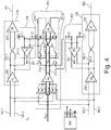
- FIG. 4 is an example diagram illustrating automatic-zeroing (calibration) of a compensation-setting generator according to embodiments herein.
- the controller 140 in phase Q1, such as between time T1 and T2 for cycle #1, the controller 140 produces switch control output 321 to be a high state to activate the group of switches S31, S32, S33, and S34 to an ON state.
- the controller 140 produces switch control output 322 as a low state to deactivate the group of switches S11, S12, S13, and S14 to an OFF state.
- the controller 140 produces switch control output 323 to be in a low state to deactivate the group of switches S21, S22, S23, and S24 to an OFF state.
- Activation of switches S31 and S32 to ON states causes the reference voltage Vref to be inputted to both the inverting out and non-inverting node of amplifier A4.
- the magnitude of Vref can be any suitable value. If amplifier A4 was an ideal operational amplifier, applying the same input voltage value to both the inverting and non-inverting would result in generation of the same output voltage for voltage 210-1 and voltage 210-2. However, due to the input referred offset voltage associated with amplifier A4, the magnitude of voltage 210-1 and voltage 210-2 are different.
- the amplifier A4 produces a respective output voltage 210-1 that is conveyed through switch S33 (activated to ON state as well) to the inverting input of transconductance amplifier A5 and storage circuit (capacitor C3).
- Capacitor C3 stores the generated voltage 210-1.
- Amplifier A4 produces a respective output voltage 210-2 that is conveyed through switch S34 (activated to ON state) to the non-inverting input of transconductance amplifier A5 and storage circuit (capacitor C4). Capacitor C4 stores the voltage 210-2.
- phase Q1 provide auto-zeroing of the amplifier A4 for subsequent use in phase Q2 used to update and generate the amplifier compensation setting 112 stored in capacitors C5 and C6.
- the storage circuit (such as capacitors C3 and C4) store a compensation value (such as one or more voltage values) that are used to correct input referred offset associated with the amplifier A4 when the amplifier A4 is subsequently used to generate the amplifier compensation setting 112 in following phase Q2.
- FIG. 5 is an example diagram illustrating generation of a first amplifier compensation setting according to embodiments herein.
- the controller 140 in phase Q2, such as between time T2 and T3 for cycle #1, the controller 140 produces switch control output 322 to be a high state to activate the switches S11, S12, S13, and S14 to an ON state.
- the controller 140 produces switch control output 323 to be a low state to deactivate the switches S21, S22, S23, and S24 to an OFF state.
- the controller 140 produces switch control output 321 to be a low state to deactivate the switches S31, S32, S33, and S34 to an OFF state.
- the controller 140 is operable to: electrically couple the compensation-setting generator 110 to the input of the second amplifier 132, and electrically decouple (via deactivation of switches S21 and S22) the compensation-setting generator 110 from an input of the first amplifier 131.
- the amplifier A4 produces a respective output voltage 210-1 that is conveyed through switch S13 (activated to ON state) to the non-inverting input of transconductance amplifier A5 and storage circuit (capacitor C5). Capacitor C5 stores the voltage 210-1.
- the amplifier A4 also produces a respective output voltage 210-2 that is conveyed through switch S14 (activated to ON state) to the inverting input of transconductance amplifier A8 and storage circuit (capacitor C6). Capacitor C6 stores the voltage 210-2.
- the prior stored voltage in capacitors C5 and C6 causes the transconductance amplifier A8 to provide correction to the voltage 210-1 and voltage 210-2 generated by the amplifier A4. Accordingly, the prior stored voltage in capacitors C3 and C4 provides correction to the amplifier A4 when generating the amplifier compensation setting 112 stored in capacitors C5 and C6 during phase Q2.
- FIG. 6 is an example diagram illustrating an automatic-zeroing (calibration) of the compensation-setting generator according to embodiments herein.
- the controller 140 in phase Q3, such as between time T3 and T4 for cycle #1, the controller 140 produces switch control output 321 to be a high state to activate the switches S31, S32, S33, and S34 to an ON state.
- the controller 140 produces switch control output 322 to be a low state to deactivate the switches S11, S12, S13, and S14 to an OFF state.
- the controller 140 produces switch control output 322 to be a low state to deactivate the switches S21, S22, S23, and S24 to an OFF state.
- switches S31 and S32 Activation of switches S31 and S32 to ON states causes the reference voltage Vref to be inputted to both the inverting out and non-inverting node of amplifier A4.
- the amplifier A4 produces a respective output voltage 210-1 that is conveyed through switch S33 (activated to ON state as well) to the inverting input of transconductance amplifier A5 and storage circuit capacitor C3.
- Capacitor C3 stores the voltage 210-1.
- Amplifier A4 produces a respective output voltage 210-2 that is conveyed through switch S34 (activated to ON state) to the non-inverting input of transconductance amplifier A5 and storage circuit capacitor C4.
- Capacitor C4 stores the voltage 210-2.
- phase Q1 provide auto-zeroing of the amplifier A4 for subsequent use in phase Q4 used to update and generate the amplifier compensation setting 111 stored in capacitors C1 and C2.
- the storage circuit (such as capacitors C3 and C4) store a compensation value (such as voltage values) that are used to correct input referred offset associated with the amplifier A4 when the amplifier A4 is subsequently used to generate the amplifier compensation setting 111 in following phase Q4.
- FIG. 7 is an example diagram illustrating generation of a second amplifier compensation setting according to embodiments herein.
- the controller 140 produces switch control output 323 to be a high state to activate the switches S21, S22, S23, and S24 to an ON state.
- the controller 140 produces switch control output 322 to be a low state to deactivate the switches S21, S22, S23, and S24 to an OFF state.
- the controller 140 produces switch control output 321 to be a low state to deactivate the switches S31, S32, S33, and S34 to an OFF state.
- the controller 140 is operable to: electrically couple the compensation-setting generator 110 to the input of the first amplifier 131, and electrically decouple (via deactivation of switches S11 and S12) the compensation-setting generator 110 from an input of the second amplifier 132.
- the amplifier A4 produces a respective output voltage 210-1 that is conveyed through switch S23 (activated to ON state) to the inverting input of transconductance amplifier A3 and storage circuit (capacitor C2).
- Capacitor C2 stores the voltage 210-1.
- the amplifier A4 also produces a respective output voltage 210-2 that is conveyed through switch S24 (activated to ON state) to the non-inverting input of transconductance amplifier A3 and capacitor C1.
- Capacitor C1 stores the voltage 210-2.
- the prior stored voltage in capacitors C3 and C4 causes the transconductance amplifier A5 to provide correction to the voltage 210-1 and voltage 210-2 generated by the amplifier A4. Accordingly, the prior stored voltage in capacitors C3 and C4 provides correction to the amplifier A4 when generating the amplifier compensation setting 111 stored in capacitors C1 and C2 during phase Q4.
- FIG. 8 is an example diagram illustrating a more specific implementation of an amplifier and compensator according to embodiments herein. As shown in this example embodiment, and as previously discussed, transconductance amplifier A3 provides correction to amplifier 131 including amplifier A1 and A2. Amplifier 132 can be configured to include similar circuitry.
- FIG. 9 is an example diagram illustrating a more specific implementation of a compensation-setting generator according to embodiments herein. As shown in this example embodiment, and as previously discussed, transconductance amplifier A5 provides correction to amplifier A4 in the compensation setting generator 110.
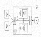
- FIG. 10 is an example block diagram of a computer device for implementing any of the operations as discussed herein according to embodiments herein.
- computer system 1000 (such as implemented by any of one or more resources such as controller 140, compensation setting generator 110, compensator 121, etc.) of the present example includes an interconnect 1011 that couples computer readable storage media 1012 such as a non-transitory type of media (or hardware storage media) in which digital information can be stored and retrieved, a processor 1013 (e.g., computer processor hardware such as one or more processor devices), I/O interface 1014, and a communications interface 1017.
- I/O interface 1014 provides connectivity to any suitable circuitry such as each of phases 110.
- Computer readable storage medium 1012 can be any hardware storage resource or device such as memory, optical storage, hard drive, floppy disk, etc. In one embodiment, the computer readable storage medium 1012 stores instructions and/or data used by the control application 140-1 to perform any of the operations as described herein.
- communications interface 1018 enables the computer system 1000 and processor 1013 to communicate over a resource such as network 193 to retrieve information from remote sources and communicate with other computers.
- computer readable storage media 1012 is encoded with control application 140-1 (e.g., software, firmware, etc.) executed by processor 1013.
- Control application 140-1 can be configured to include instructions to implement any of the operations as discussed herein.
- processor 1013 accesses computer readable storage media 1012 via the use of interconnect 1011 in order to launch, run, execute, interpret or otherwise perform the instructions in control application 140-1 stored on computer readable storage medium 1012.
- Execution of the control application 140-1 produces processing functionality such as control process 140-2 in processor 1013.
- the control process 140-2 associated with processor 1013 represents one or more aspects of executing control application 140-1 within or upon the processor 1013 in the computer system 1000.
- computer system 1000 can be a micro-controller device, logic, hardware processor, hybrid analog/dif circuitry, etc., configured to control a power supply and perform any of the operations as described herein.
- FIG. 11 is an example diagram illustrating a method according to embodiments herein.
- the controller 140 controls compensation-setting generator 110 to generate a first amplifier compensation setting 111 and a second amplifier compensation setting 112 (during different time slots).
- the first amplifier compensation setting 111 is generated to correct an input offset voltage associated with first amplifier 131;
- the second amplifier compensation setting 112 is generated to correct an input offset voltage associated with second amplifier 132.
- the controller 140 applies the first amplifier compensation setting 111 to the first amplifier 131.
- the controller 140 applies the second amplifier compensation setting 112 to the second amplifier 132.
- the controller 140 switches between updating the first compensation setting 111 applied to the first compensator 121 and the second compensation setting 112 applied to the second amplifier 132.
- An algorithm as described herein, and generally, is considered to be a self-consistent sequence of operations or similar processing leading to a desired result.
- operations or processing involve physical manipulation of physical quantities.
- quantities may take the form of electrical or magnetic signals capable of being stored, transferred, combined, compared or otherwise manipulated. It has been convenient at times, principally for reasons of common usage, to refer to such signals as bits, data, values, elements, symbols, characters, terms, numbers, numerals or the like. It should be understood, however, that all of these and similar terms are to be associated with appropriate physical quantities and are merely convenient labels.
Landscapes
- Engineering & Computer Science (AREA)
- Power Engineering (AREA)
- Multimedia (AREA)
- Microelectronics & Electronic Packaging (AREA)
- Amplifiers (AREA)
Applications Claiming Priority (1)
| Application Number | Priority Date | Filing Date | Title |
|---|---|---|---|
| US15/948,398 US10651797B2 (en) | 2018-04-09 | 2018-04-09 | Amplifier offset and compensation |
Publications (1)
| Publication Number | Publication Date |
|---|---|
| EP3553949A1 true EP3553949A1 (de) | 2019-10-16 |
Family
ID=65991699
Family Applications (1)
| Application Number | Title | Priority Date | Filing Date |
|---|---|---|---|
| EP19165379.9A Pending EP3553949A1 (de) | 2018-04-09 | 2019-03-27 | Verstärker-offset und -kompensation |
Country Status (3)
| Country | Link |
|---|---|
| US (1) | US10651797B2 (de) |
| EP (1) | EP3553949A1 (de) |
| CN (1) | CN110365300B (de) |
Families Citing this family (3)
| Publication number | Priority date | Publication date | Assignee | Title |
|---|---|---|---|---|
| BR112018001247A2 (pt) * | 2015-09-01 | 2018-07-24 | Nec Corporation | aparelho de amplificação de energia e sistema de transmissão de sinal de televisão |
| TWI885667B (zh) * | 2022-12-30 | 2025-06-01 | 新加坡商光寶科技新加坡私人有限公司 | 偏移電壓補償電路及包括其之隔離放大器裝置 |
| US20250202445A1 (en) * | 2023-12-18 | 2025-06-19 | Cirrus Logic International Semiconductor Ltd. | Feedforward offset cancellation of analog amplifier using output auto-zeroed gain stages |
Citations (4)
| Publication number | Priority date | Publication date | Assignee | Title |
|---|---|---|---|---|
| US7605647B1 (en) * | 2008-04-29 | 2009-10-20 | Allegro Microsystems, Inc. | Chopper-stabilized amplifier and magnetic field sensor |
| US20130015916A1 (en) * | 2011-07-12 | 2013-01-17 | Analog Devices, Inc. | Common-Mode Amplifier Step Response |
| US20150288336A1 (en) * | 2014-04-08 | 2015-10-08 | Analog Devices, Inc. | Apparatus and methods for multi-channel autozero and chopper amplifiers |
| US20160013760A1 (en) * | 2014-07-14 | 2016-01-14 | Skyworks Solutions, Inc. | Circuits and devices related to fast turn-on of radio-frequency amplifiers |
Family Cites Families (26)
| Publication number | Priority date | Publication date | Assignee | Title |
|---|---|---|---|---|
| FR2473810A1 (fr) | 1980-01-09 | 1981-07-17 | Ibm France | Procede de compensation de la tension de decalage d'un amplificateur differentiel et macro-fonctionnelle en resultant |
| US5336986A (en) * | 1992-02-07 | 1994-08-09 | Crosspoint Solutions, Inc. | Voltage regulator for field programmable gate arrays |
| JPH05243864A (ja) | 1992-02-29 | 1993-09-21 | Sony Corp | 差動増幅回路 |
| US6140872A (en) * | 1999-10-28 | 2000-10-31 | Burr-Brown Corporation | Offset-compensated amplifier input stage and method |
| US6515464B1 (en) | 2000-09-29 | 2003-02-04 | Microchip Technology Incorporated | Input voltage offset calibration of an analog device using a microcontroller |
| US6714886B2 (en) * | 2002-02-13 | 2004-03-30 | Eric C. Sung | System and method of DC calibration of amplifiers |
| US7132882B2 (en) | 2002-07-19 | 2006-11-07 | Avago Technologies Fiber Ip (Singapore) Pte. Ltd. | Amplifier having multiple offset-compensation paths and related systems and methods |
| DE10345100B4 (de) * | 2003-09-26 | 2012-03-29 | Austriamicrosystems Ag | Differenzverstärkeranordnung |
| US7242330B2 (en) | 2003-12-17 | 2007-07-10 | Texas Instruments Incorporated | Dynamic compensation of analog-to-digital converter (ADC) offset errors using filtered PWM |
| US7034608B2 (en) | 2004-02-20 | 2006-04-25 | Fujitsu Limited | Correcting DC offsets in a multi-stage amplifier |
| DE102005007632A1 (de) * | 2005-02-18 | 2006-08-24 | Infineon Technologies Ag | Verstärkeranordnung und Verfahren zum Abgleichen eines Offsets |
| US7835467B2 (en) * | 2006-01-05 | 2010-11-16 | Qualcomm, Incorporated | DC offset correction for high gain complex filter |
| JP4978022B2 (ja) * | 2006-02-16 | 2012-07-18 | 富士通セミコンダクター株式会社 | 演算増幅器 |
| US7514978B2 (en) | 2006-05-08 | 2009-04-07 | Mellanox Technologies Ltd. | Terminated input buffer with offset cancellation circuit |
| US7541792B2 (en) * | 2006-10-31 | 2009-06-02 | Semiconductor Components Industries, L.L.C. | Compensated switching power supply controller and method therefor |
| US7564397B2 (en) * | 2007-04-10 | 2009-07-21 | Micron Technology, Inc. | High slew rate amplifier, analog-to-digital converter using same, CMOS imager using the analog-to-digital converter and related methods |
| EP2075910A1 (de) * | 2007-12-28 | 2009-07-01 | Varian B.V. | Instrumentenverstärkung mit Eingabe-Offset-Regulierung |
| JP5144308B2 (ja) * | 2008-02-25 | 2013-02-13 | ラピスセミコンダクタ株式会社 | オペアンプ回路及びオペアンプ回路の駆動方法 |
| US7944288B2 (en) * | 2008-09-29 | 2011-05-17 | Infineon Technologies Ag | Switched-capacitor amplifier arrangement having a low input current |
| US7812665B2 (en) * | 2009-02-23 | 2010-10-12 | Number 14 B.V. | Amplifiers with input offset trim and methods |
| US7973596B2 (en) * | 2009-05-12 | 2011-07-05 | Number 14 B.V. | Low-noise, low-power, low drift offset correction in operational and instrumentation amplifiers |
| KR20120121779A (ko) * | 2011-04-27 | 2012-11-06 | 삼성전기주식회사 | 자기 검출 회로의 오프셋 보상 장치 및 그 방법 |
| TWI524074B (zh) | 2013-12-13 | 2016-03-01 | 財團法人國家實驗研究院 | 偏移補償電路及其補償方法 |
| US9385673B2 (en) | 2014-02-14 | 2016-07-05 | Analog Devices Global | Amplifier with offset compensation |
| US9780736B1 (en) * | 2016-03-30 | 2017-10-03 | Synaptics Incorporated | Temperature compensated offset cancellation for high-speed amplifiers |
| US10044327B2 (en) * | 2016-09-09 | 2018-08-07 | Analog Devices Global | Fast settling capacitive gain amplifier circuit |
-
2018
- 2018-04-09 US US15/948,398 patent/US10651797B2/en active Active
-
2019
- 2019-03-27 EP EP19165379.9A patent/EP3553949A1/de active Pending
- 2019-04-09 CN CN201910280727.2A patent/CN110365300B/zh active Active
Patent Citations (4)
| Publication number | Priority date | Publication date | Assignee | Title |
|---|---|---|---|---|
| US7605647B1 (en) * | 2008-04-29 | 2009-10-20 | Allegro Microsystems, Inc. | Chopper-stabilized amplifier and magnetic field sensor |
| US20130015916A1 (en) * | 2011-07-12 | 2013-01-17 | Analog Devices, Inc. | Common-Mode Amplifier Step Response |
| US20150288336A1 (en) * | 2014-04-08 | 2015-10-08 | Analog Devices, Inc. | Apparatus and methods for multi-channel autozero and chopper amplifiers |
| US20160013760A1 (en) * | 2014-07-14 | 2016-01-14 | Skyworks Solutions, Inc. | Circuits and devices related to fast turn-on of radio-frequency amplifiers |
Also Published As
| Publication number | Publication date |
|---|---|
| CN110365300B (zh) | 2025-03-04 |
| US10651797B2 (en) | 2020-05-12 |
| CN110365300A (zh) | 2019-10-22 |
| US20190312551A1 (en) | 2019-10-10 |
Similar Documents
| Publication | Publication Date | Title |
|---|---|---|
| JP5108449B2 (ja) | 容量素子バラツキ依存性のないスイッチドキャパシタ増幅器およびその動作方法 | |
| CN110365300B (zh) | 用于放大器补偿的设备、方法及计算机可读存储介质 | |
| US6577188B2 (en) | Variable gain amplifier | |
| US20080150368A1 (en) | Configurable power supply integrated circuit | |
| US12407260B2 (en) | Power supply system apparatus | |
| US20230213954A1 (en) | System level offset calibration of multiphase voltage regulator | |
| US11916516B2 (en) | Low power operational amplifier trim offset circuitry | |
| US20050285682A1 (en) | Amplifying circuit with variable supply voltage | |
| JP2017076878A (ja) | オーディオ回路、それを用いた電子機器 | |
| JP7000804B2 (ja) | 電源装置 | |
| CN101366169A (zh) | 用于高增益复数滤波器的dc偏移校正 | |
| WO2021192378A1 (ja) | マルチコンバータ電源システム | |
| WO2021192377A1 (ja) | マルチコンバータ電源システム | |
| JP2006319388A (ja) | 自動利得制御回路及びそれを用いた正弦波発振回路 | |
| US20200304076A1 (en) | Trans impedance amplifier capacitance isolation stage | |
| JP5732031B2 (ja) | パイプライン型a/dコンバータ | |
| CN108291936B (zh) | 一种用于提供电流脉冲的电路和方法 | |
| US20190326923A1 (en) | Multi-Ladder Digital to Analog Converter | |
| CN105373179A (zh) | 电压发生电路和极坐标发射器 | |
| TWI429193B (zh) | 放大器電路及偏移消除方法 | |
| US11070178B1 (en) | Class D power amplifier | |
| US7652536B2 (en) | Amplifier circuit with internal zeros | |
| JP6349789B2 (ja) | 補正装置、電圧検出装置、及び電力測定システム | |
| JP4461480B2 (ja) | 増幅器 | |
| CN108988810B (zh) | 用于放大器校准的方法和系统 |
Legal Events
| Date | Code | Title | Description |
|---|---|---|---|
| PUAI | Public reference made under article 153(3) epc to a published international application that has entered the european phase |
Free format text: ORIGINAL CODE: 0009012 |
|
| STAA | Information on the status of an ep patent application or granted ep patent |
Free format text: STATUS: THE APPLICATION HAS BEEN PUBLISHED |
|
| AK | Designated contracting states |
Kind code of ref document: A1 Designated state(s): AL AT BE BG CH CY CZ DE DK EE ES FI FR GB GR HR HU IE IS IT LI LT LU LV MC MK MT NL NO PL PT RO RS SE SI SK SM TR |
|
| AX | Request for extension of the european patent |
Extension state: BA ME |
|
| STAA | Information on the status of an ep patent application or granted ep patent |
Free format text: STATUS: REQUEST FOR EXAMINATION WAS MADE |
|
| STAA | Information on the status of an ep patent application or granted ep patent |
Free format text: STATUS: EXAMINATION IS IN PROGRESS |
|
| 17P | Request for examination filed |
Effective date: 20200416 |
|
| RBV | Designated contracting states (corrected) |
Designated state(s): AL AT BE BG CH CY CZ DE DK EE ES FI FR GB GR HR HU IE IS IT LI LT LU LV MC MK MT NL NO PL PT RO RS SE SI SK SM TR |
|
| 17Q | First examination report despatched |
Effective date: 20200520 |
|
| GRAP | Despatch of communication of intention to grant a patent |
Free format text: ORIGINAL CODE: EPIDOSNIGR1 |
|
| STAA | Information on the status of an ep patent application or granted ep patent |
Free format text: STATUS: GRANT OF PATENT IS INTENDED |