EP3552310B1 - Dispositif de commande d'un élément semi-conducteur de puissance commutable bipolaire, module semi-conducteur et procédé - Google Patents
Dispositif de commande d'un élément semi-conducteur de puissance commutable bipolaire, module semi-conducteur et procédé Download PDFInfo
- Publication number
- EP3552310B1 EP3552310B1 EP17804821.1A EP17804821A EP3552310B1 EP 3552310 B1 EP3552310 B1 EP 3552310B1 EP 17804821 A EP17804821 A EP 17804821A EP 3552310 B1 EP3552310 B1 EP 3552310B1
- Authority
- EP
- European Patent Office
- Prior art keywords
- voltage
- power semiconductor
- semiconductor component
- control device
- value
- Prior art date
- Legal status (The legal status is an assumption and is not a legal conclusion. Google has not performed a legal analysis and makes no representation as to the accuracy of the status listed.)
- Active
Links
- 239000004065 semiconductor Substances 0.000 title claims description 126
- 238000000034 method Methods 0.000 title claims description 19
- 230000004913 activation Effects 0.000 claims description 3
- 239000002800 charge carrier Substances 0.000 description 13
- 230000003213 activating effect Effects 0.000 description 3
- 230000001419 dependent effect Effects 0.000 description 2
- 238000011161 development Methods 0.000 description 2
- 230000018109 developmental process Effects 0.000 description 2
- 238000010586 diagram Methods 0.000 description 2
- 230000007704 transition Effects 0.000 description 2
- 238000007599 discharging Methods 0.000 description 1
- 230000005684 electric field Effects 0.000 description 1
- 238000005259 measurement Methods 0.000 description 1
Images
Classifications
-
- H—ELECTRICITY
- H03—ELECTRONIC CIRCUITRY
- H03K—PULSE TECHNIQUE
- H03K17/00—Electronic switching or gating, i.e. not by contact-making and –breaking
- H03K17/16—Modifications for eliminating interference voltages or currents
- H03K17/168—Modifications for eliminating interference voltages or currents in composite switches
-
- H—ELECTRICITY
- H03—ELECTRONIC CIRCUITRY
- H03K—PULSE TECHNIQUE
- H03K17/00—Electronic switching or gating, i.e. not by contact-making and –breaking
-
- H—ELECTRICITY
- H03—ELECTRONIC CIRCUITRY
- H03K—PULSE TECHNIQUE
- H03K17/00—Electronic switching or gating, i.e. not by contact-making and –breaking
- H03K17/04—Modifications for accelerating switching
- H03K17/041—Modifications for accelerating switching without feedback from the output circuit to the control circuit
- H03K17/0412—Modifications for accelerating switching without feedback from the output circuit to the control circuit by measures taken in the control circuit
- H03K17/04126—Modifications for accelerating switching without feedback from the output circuit to the control circuit by measures taken in the control circuit in bipolar transistor switches
-
- H—ELECTRICITY
- H03—ELECTRONIC CIRCUITRY
- H03K—PULSE TECHNIQUE
- H03K17/00—Electronic switching or gating, i.e. not by contact-making and –breaking
- H03K17/04—Modifications for accelerating switching
- H03K17/041—Modifications for accelerating switching without feedback from the output circuit to the control circuit
- H03K17/0412—Modifications for accelerating switching without feedback from the output circuit to the control circuit by measures taken in the control circuit
- H03K17/0414—Anti-saturation measures
-
- H—ELECTRICITY
- H03—ELECTRONIC CIRCUITRY
- H03K—PULSE TECHNIQUE
- H03K17/00—Electronic switching or gating, i.e. not by contact-making and –breaking
- H03K17/04—Modifications for accelerating switching
- H03K17/042—Modifications for accelerating switching by feedback from the output circuit to the control circuit
- H03K17/0422—Anti-saturation measures
-
- H—ELECTRICITY
- H03—ELECTRONIC CIRCUITRY
- H03K—PULSE TECHNIQUE
- H03K17/00—Electronic switching or gating, i.e. not by contact-making and –breaking
- H03K17/16—Modifications for eliminating interference voltages or currents
- H03K17/161—Modifications for eliminating interference voltages or currents in field-effect transistor switches
- H03K17/162—Modifications for eliminating interference voltages or currents in field-effect transistor switches without feedback from the output circuit to the control circuit
- H03K17/163—Soft switching
Definitions
- the present invention relates to a control device for driving a bipolar switchable power semiconductor component, the control device being designed to apply an electrical voltage to a gate terminal of the power semiconductor component and to reduce the electrical voltage for switching off the power semiconductor component from a first voltage value to a second voltage value.
- the present invention also relates to a semiconductor module having such a control device.
- the present invention relates to a method for controlling a bipolar switchable power semiconductor component.
- bipolar switchable or switchable power semiconductor components can in particular be an IGBT.
- IGBT In the present case, the interest is directed towards bipolar switchable or switchable power semiconductor components.
- Such a bipolar switchable power semiconductor component can in particular be an IGBT.
- bipolar switchable power semiconductor components When bipolar switchable power semiconductor components are switched off, the charge carriers required for the flow of current are removed.
- IGBTs In switching off conventional and reverse-conductive IGBTs, high electrical field strengths arise due to the removal of the charge carriers. Due to this field strength load, the power semiconductor component cannot be switched off as quickly as desired.
- the rate of increase of the electrical voltage at the load connections is primarily limited by the requirements of the load.
- Both the charge carrier concentration in the power semiconductor component and the switching speed influence the turn-off losses of the power semiconductor component.
- the switching speed is limited by the safe working area to be maintained to minimize losses set as high as possible. This is usually done via a suitable choice of the level of a gate discharge current.
- the gate of the switched-on power semiconductor component is charged to an electrical voltage with a first voltage value.
- the gate is discharged via a resistor to an electrical voltage with a second voltage value.
- the electrical voltage is thus reduced from the first voltage value to the second voltage value.
- a control device is used to control a bipolar switchable power semiconductor component.
- the control device is designed to apply an electrical voltage to a gate connection of the power semiconductor component to apply and to reduce the electrical voltage for switching off the power semiconductor component from a first voltage value to a second voltage value.
- the control device is designed to switch off the power semiconductor component to first reduce the electrical voltage from the first voltage value to a desaturation value and then to reduce the electrical voltage from the desaturation value to the second voltage value, the desaturation value being greater than a pinch-off voltage of the power semiconductor component.
- a bipolar switchable or switchable power semiconductor component can be controlled with the aid of the control device.
- the control device can, for example, be part of a control circuit.
- the power semiconductor component can in particular be a bipolar transistor with an insulated gate connection (insulated gate bipolar transistor, IGBT).
- the control device is electrically connected to the gate electrode or the gate connection of the power semiconductor component. It can be provided that the control device has a gate resistor that is connected to the gate terminal of the power semiconductor component.
- electrical voltages with different voltage values can be provided or applied to the gate connection. For example, the electrical voltage with the first voltage value can be applied to the gate connection in order to switch on the power semiconductor component.
- the electrical voltage with the first voltage value When the electrical voltage with the first voltage value is applied to the gate connection, it is provided in particular that a gate-emitter voltage of the power semiconductor component is above a threshold value. In this case, the power semiconductor component is in the on state. If the power semiconductor component is to be switched off, the electrical voltage is reduced from the first voltage value to the second voltage value by means of the control device.
- the electrical voltage at the gate connection is initially reduced from the first voltage value to the desaturation value and then reduced to the second voltage value.
- the electrical voltage at the gate connection or the gate-emitter voltage is not reduced directly to the second voltage value, but rather the electrical voltage is initially set to the desaturation value.
- the desaturation value is smaller than the first voltage value and larger than the second voltage value.
- a desaturation pulse can be provided at the gate connection shortly before the actual switch-off process. This desaturation pulse discharges the gate or the gate connection of the power semiconductor component to a voltage which is slightly above the pinch-off voltage of the power semiconductor component.
- pinch-off tension can also be referred to as pinchoff tension. If the pinch-off voltage is applied to the power semiconductor component, a channel of the power semiconductor component is constricted. Because the electrical voltage at the gate terminal is initially reduced to the desaturation value, the charge carrier concentration within the power semiconductor component can be reduced. Thus, when the power semiconductor component is switched off, less charge has to be removed from the power semiconductor component. The turn-off losses when the power semiconductor component is turned off can thus be reduced and the turn-off process can thus be carried out more efficiently.
- the control device has a first switch for applying the electrical voltage with the first voltage value to the gate connection and a second switch for applying the electrical voltage with the second voltage value to the gate connection.
- the first switch and the second switch can be controlled independently of one another.
- the first switch is used to connect the gate to the to connect electrical voltage with the first voltage value.
- the second switch is used to connect the gate connection to the electrical voltage with the second voltage value.
- the respective switches can be used, for example, to switch an electrical connection between the gate connection and a voltage source which provide the electrical voltage with the first voltage value or the second voltage value. It can also be provided that the gate connection is connected to a voltage sink by means of the switches.
- the control device is designed to control the first switch and / or the second switch periodically and to set the electrical voltage to the desaturation value by specifying a duty cycle for the control of the first switch and / or the second switch.
- the electrical voltage can be provided at the gate connection in the manner of pulse width modulation.
- the lowering of the gate-emitter voltage can therefore be achieved by pulse width modulation.
- the voltage at the gate connection of the power semiconductor component is set to the desaturation value by means of a suitable pulse-pause ratio. This enables a reliable setting of the electrical voltage at the gate connection.
- control device has a measuring unit for measuring a collector current at a collector connection of the power semiconductor component and the control device is designed to determine the desaturation value on the basis of the collector current.
- the desaturation value can be determined on the basis of the pinch-off voltage or the pinchoff voltage of the power semiconductor component.
- the pinch-off voltage can be determined from the relationship between the collector current and the gate-emitter voltage. It is provided in particular that the collector current is measured before the power semiconductor component is switched off and the desaturation value or the electrical voltage is determined with the desaturation value in such a way that that this is very close to the pinch-off tension or slightly exceeds the pinch-off tension. This enables the desaturation value to be reliably determined.
- the control device is preferably designed to apply the electrical voltage with the desaturation value for a predetermined pulse duration to the gate connection.
- the electrical voltage with the desaturation value is maintained or applied to the gate connection until the charge carriers in the power semiconductor component are reduced. While the electrical voltage with the desaturation value is being applied to the power semiconductor component, the excess charge is immediately removed by the load current. At the same time, the charge carriers recombine, which happens much more slowly. Meanwhile, the forward voltage also rises.
- the pulse duration during which the electrical voltage with the desaturation value is applied to the power semiconductor component can be predetermined. The pulse duration can, for example, be determined on the basis of measurements carried out previously. An efficient shutdown process can thus be achieved.
- the control device has a measuring unit for measuring a gate-emitter voltage between the gate connection and an emitter connection of the power semiconductor component during shutdown and the control device is designed to assign the pulse duration based on the gate-emitter voltage determine. It can therefore be provided that the gate-emitter voltage is measured continuously during the switch-off process.
- the gate-emitter voltage describes the electrical voltage that is applied to the gate connection of the power semiconductor component by means of the control device.
- the output of the voltage by means of the control device or the gate-emitter voltage can be continuously determined and consequently the pulse duration can be set precisely.
- the control device is designed to open the first switch to turn off the power semiconductor component, then to close the second switch for a first period of time, then to open the second switch for a second period of time and then to close the second switch.
- the first switch can be closed at a first point in time and the second switch can be opened at the same time. After the first period of time, the second switch can be opened again. The second switch remains open for the second period of time.
- the first time period and the second time period are selected such that the total desaturation value for the voltage at the gate connection results.
- the sum of the first duration and the second duration corresponds in particular to the pulse duration.
- the second time period represents a high-resistance control or a switchover to a high-resistance gate resistor.
- the second switch can then be opened again at a second point in time in order to completely discharge the gate.
- the electrical voltage at the gate connection can thus be controlled with the aid of the first and the second switch.
- the control device has a third switch for applying the electrical voltage with the desaturation value, and the control device is designed to open the first switch and close the third switch at a first point in time and the third at a second point in time Switch to open and the second switch to close.
- the first switch is closed.
- the first switch is opened at the first point in time and the third switch is closed at the same time.
- the electrical voltage with the desaturation value is thus applied to the gate connection.
- the third switch is opened and at a second point in time the second switch closed.
- the electrical voltage with the second voltage value is thus applied to the gate connection.
- the power semiconductor component can thus be switched off with reduced switching losses.
- control device has an analog amplifier for providing the electrical voltage with the first voltage value, the desaturation value and the second voltage value.
- the analog amplifier can be designed as an analog amplifier output stage, by means of which the electrical voltage at the gate connection can be continuously adjusted. With such a type of output stage, theoretically far-reaching optimized gate voltage trajectories can be set. Regulation of the current and / or voltage transients of the power semiconductor component to be controlled can thus also be made possible.
- a semiconductor module according to the invention comprises a bipolar switchable power semiconductor component and a control device according to the invention.
- the control device according to the invention serves to control the bipolar switchable power semiconductor component.
- the power semiconductor component can in particular be a bipolar transistor with an insulated gate electrode or with an insulated gate connection.
- the power semiconductor component can therefore be designed as an IGBT.
- the semiconductor module can be a converter, for example. It is provided in particular that the pulse duration during which the electrical voltage with the desaturation value is applied to the power semiconductor component is taken into account in the control rate of the converter, since this acts as an additional switch-off delay.
- a method according to the invention is used to control a bipolar switchable power semiconductor component.
- an electrical voltage is applied to a gate connection of the power semiconductor component by means of a control device and the electrical voltage is used to switch off of the power semiconductor component reduced from a first voltage value to a second voltage value. It is provided that the electrical voltage for switching off the power semiconductor component is initially reduced from the first voltage value to a desaturation value and the electrical voltage is then reduced from the desaturation value to the second voltage value, the desaturation value being greater than a pinch-off voltage of the power semiconductor component.
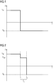
- FIG. 12 shows a profile of an electrical voltage U as a function of time t, which is applied to a gate connection of the power semiconductor component 1 while a power semiconductor component 1 is switched off.
- the electrical voltage U describes the voltage in front of a possible gate discharge resistor, which is usually arranged between the gate connection of the power semiconductor component 1 and the control device 2.
- the course of the voltage U which in FIG 1 is shown, a shutdown process according to the prior art.
- an electrical voltage U with a first voltage value U B + is applied to the gate connection.
- the first voltage value U B + can be a positive electrical voltage.
- the electrical voltage U is reduced from the first voltage value U B + to a second voltage value U B- .
- the second voltage value U B- can be assigned to a negative electrical voltage, for example.
- the direct transition from the conductive state with a high charge carrier concentration to the currentless state results in comparatively high turn-off losses.
- FIG 2 shows the course of the electrical voltage U as a function of the time t during a shutdown process according to an embodiment of the invention.
- the electrical voltage U at the gate connection is reduced from the first voltage value U B + to a desaturation value U sat and then to the second voltage value U B- .
- the electrical voltage U with the desaturation value U sat is applied to the gate connection for a predetermined pulse duration t p .
- the pulse duration t p begins at a first point in time t1 and ends at a second point in time t2. Because the electrical voltage U at the gate terminal is initially reduced to the desaturation value U sat , the charge carrier concentration can be reduced before the actual shutdown process of the power semiconductor component 1. As a result, less charge has to be removed from the power semiconductor component 1 during the shutdown process. As a result, the shutdown losses decrease.
- the desaturation value U sat is determined in such a way that it is slightly above a load current-dependent pinch-off voltage U P of the power semiconductor component 1.
- This pinch-off voltage U P can also be referred to as the pinchoff voltage.
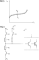
- FIG 3 shows a profile of the pinch-off voltage U P and the profile of the desaturation value U sat .
- the diagram in FIG 3 the gate-emitter voltage U GE as a function of the collector current I C.
- the desaturation value U sat can have a fixed level, which corresponds at least to the maximum expected pinch-off voltage U P.
- the desaturation value U sat can also be set very close to the pinch-off voltage U P by measuring the collector current I C before switching off. However, this requires an adjustable voltage source or voltage sink.
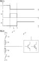
- FIG 4 shows a semiconductor module 3 according to a first embodiment.
- the semiconductor module 3 comprises a control device 2 and the power semiconductor component 1.
- the power semiconductor component 1 can be designed as a conventional or reverse-conductive IGBT.
- An equivalent circuit diagram of the reverse conductive IGBT for the power semiconductor component 1 is shown here by way of example.
- the control device 2 comprises a first switch S1, via which, with the interposition of a first resistor R1, the power semiconductor component 1 with an electrical voltage U with the first Voltage value U B + can be connected.
- the control device 2 comprises a second switch S2, via which the power semiconductor component 1 can be connected to an electrical voltage U with the second voltage value U B- with the interposition of a second resistor R2.
- the control device 2 comprises a third switch S3, via which the power semiconductor component 1 can be connected to an electrical voltage U with the desaturation value U sat with the interposition of a third resistor R3.
- FIG 5 shows the switching curves of the switches S1, S2 and S3 of the control device 2 according to FIG FIG 4 as a function of time t.
- the first switch S1 is opened at the first point in time t1.
- the third switch S3 is closed.
- the desaturation pulse can thus be initiated for the pulse duration t p .
- the power semiconductor component 1 with a reduced charge carrier concentration and thus reduced switching losses is switched off by activating the second switch S2 alone at the second time t2.
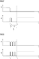
- FIG 6 shows a semiconductor module 3 according to a further embodiment.
- the control device 2 comprises only the first switch S1 and the second switch S2, which are used in connection with the switching device 2 according to FIG FIG 4 have been described.
- the further voltage level of the desaturation value U sat is not required here.
- the gate-emitter voltage U GE can be reduced by briefly, incompletely, discharging the gate.
- FIG 7 shows the switching curves of the switches S1 and S2 of the control device 2 according to FIG FIG 6 as a function of time t according to a first embodiment.
- the voltage U at the gate is thereby reduced by deactivating the first switch S1 and briefly activating the second switch S2 brought to the desaturation value U sat .
- the first switch S1 is opened and the second switch S2 is closed for the first time period t d1 .
- the first time period t d1 can either be predetermined or determined by measuring the gate-emitter voltage. It would also be possible to detect an associated increase in the collector-emitter voltage.
- both the first switch S1 and the second switch S2 are deactivated for the second time period t d2 and the control is thus switched to high resistance.
- a lower gate current can also be set by switching to a high-resistance gate resistor.
- FIG 8 shows the switching curves of the switches S1 and S2 of the control device 2 according to FIG FIG 6 as a function of time t according to a second embodiment.
- the gate-emitter voltage U GE is achieved by pulse width modulation.
- the desaturation value U sat is set at the gate connection of the power semiconductor component 1 by means of a suitable pulse-pause ratio. Before the gate of the power semiconductor component 1 is discharged to the second voltage value U B- with the second switch S2, the desaturation pulse is initiated with pulse width modulation by activating the first switch S1 and the second switch S2.
- the desaturation value U sat is set with the corresponding pulse duty factor of the first switch S1 and the second switch S2.
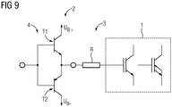
- FIG 9 shows a semiconductor module 3 according to a further embodiment.
- the control device 2 here comprises an analog amplifier 4 or an analog amplifier output stage.
- the amplifier 4 comprises a first transistor T1, via which the electrical voltage U with the first voltage value U B + with the interposition of the resistor R at the Power semiconductor component can be created.
- the amplifier 4 comprises a second transistor T2, via which the electrical voltage U with the second voltage value U B- can be applied to the power semiconductor component 1.
- the electrical voltage U can be continuously adjusted.
- the course of the electrical voltage U which in connection with FIG 2 has been explained, are applied to the gate connection of the power semiconductor component 1.
- the field strength load on the power semiconductor component 1 when it is switched off can be reduced, since the charge carrier concentration in the power semiconductor component 1 is reduced via the desaturation value U sat .
- the robustness limits or the safe working range which in particular describe higher switching speeds through a higher gate discharge current without exceeding the field strength limits, switching losses can be significantly reduced. This can be used in particular if the rate of rise of the voltage at the main terminals of the power semiconductor component 1 is not limited by the applications.
- the semiconductor modules 3 described can in particular be part of a converter. The efficiency of the converter can thus be increased by reducing the switching losses.
Landscapes
- Power Conversion In General (AREA)
- Electronic Switches (AREA)
Claims (6)
- Dispositif (2) de commande pour commander un composant (1) à semi-conducteur de puissance commutable bipolaire, le dispositif (2) de commande étant conçu pour appliquer une tension (U) électrique à une borne de grille du composant (1) à semi-conducteur de puissance et pour réduire la tension (U) électrique, afin de bloquer le composant (U) à semi-conducteur de puissance, d'une première valeur (UB+) de tension à une deuxième valeur (UB-) de tension, le dispositif (2) de commande étant conçu, afin de bloquer le composant (1) à semi-conducteur de puissance, pour réduire la tension (U) électrique de la première valeur (UB+) de tension d'abord à une valeur (Usat) de désaturation et ensuite pour réduire la tension (U) électrique de la valeur (Usat) de désaturation à la deuxième valeur (UB-) de tension, la valeur (Usat) de désaturation étant plus grande qu'une tension (Up) de blocage du composant (1) à semi-conducteur de puissance, le dispositif (2) de commande ayant un premier interrupteur (S1) pour l'application de la tension (U) électrique ayant la première valeur (UB+) de tension à la borne de grille et un deuxième interrupteur (S2) pour l'application de la tension (U) électrique ayant la deuxième valeur (UB-) de tension à la borne de grille, caractérisé en ce que le dispositif (2) de commande est conçu pour commander le premier interrupteur (S1) et/ou le deuxième interrupteur (S2) périodiquement et pour régler la tension (U) électrique à la valeur (Usat) de désaturation par prescription d'un degré d'échantillonnage de la commande du premier interrupteur (S1) et/ou du deuxième interrupteur (S2), le dispositif (2) de commande ayant une unité de mesure pour la mesure d'un courant (Ic) de collecteur à une borne de collecteur du composant (2) à semi-conducteur de puissance et le dispositif (2) de commande étant conçu pour déterminer la valeur (Usat) de désaturation à l'aide du courant (Ic) de collecteur.
- Dispositif (2) de commande suivant la revendication 1, dans lequel le dispositif (2) de commande est conçu pour appliquer à la borne de grille la tension (U) électrique ayant la valeur (Usat) de désaturation pendant une durée (tp) d'impulsion déterminée.
- Dispositif (2) de commande suivant la revendication 2, dans lequel le dispositif (2) de commande a une unité de mesure pour la mesure d'une tension (UGE) de grille-émetteur entre la borne de grille et une borne d'émetteur du composant (1) à semi-conducteur de puissance pendant le blocage et le dispositif (2) de commande est conçu pour déterminer la durée (td) d'impulsion à l'aide de la tension (UGE) de grille-émetteur.
- Module (3) à semi-conducteur, comprenant un composant (1) à semi-conducteur de puissance commutable bipolaire et comprenant un dispositif (2) de commande suivant l'une des revendications précédentes pour commander le composant (1) à semi-conducteur commutable bipolaire.
- Module (3) à semi-conducteur suivant la revendication 4, dans lequel le composant (1) à semi-conducteur de puissance commutable bipolaire est un transistor bipolaire à borne de grille isolée.
- Procédé de commande d'un composant (1) à semi-conducteur de puissance commutable bipolaire, dans lequel, au moyen d'un dispositif (2) de commande, on applique une tension (U) électrique à une borne de grille du composant (1) à semi-conducteur de puissance et on réduit la tension (U) électrique, pour le blocage du composant (1) à semi-conducteur de puissance, d'une première valeur (UB+) de tension à une deuxième valeur (UB-) de tension, la tension (U) électrique étant, pour le blocage du composant (1) à semi-conducteur de puissance, réduite de la première valeur (UB+) de tension d'abord à une valeur (Usat) de désaturation et la tension (U) électrique étant ensuite réduite de la valeur (Usat) de désaturation à la deuxième valeur (UB-) de tension, la valeur (Usat) de désaturation étant plus grande qu'une tension (Up) de blocage du composant (1) à semi-conducteur de puissance, le dispositif (2) de commande ayant un premier interrupteur (S1) pour appliquer la tension (U) électrique ayant la première valeur (UB+) de tension à la borne de grille et un deuxième interrupteur (S2) pour appliquer la tension (U) électrique ayant la deuxième valeur (UB-) de tension à la borne de grille, caractérisé en ce que l'on commande périodiquement le premier interrupteur (S1) et/ou le deuxième interrupteur (S2) et on règle la tension (U) électrique à la valeur (Usat) de désaturation en prescrivant un degré d'échantillonnage de la commande du premier interrupteur (S1) et/ou du deuxième interrupteur (S2) et, au moyen d'une unité de mesure du dispositif (2) de commande, on mesure un courant (Ic) de collecteur à une borne de collecteur du composant (2) à semi-conducteur de puissance et on détermine la valeur (Usat) de désaturation au moyen du dispositif (2) de commande à l'aide du courant (Ic) de collecteur.
Applications Claiming Priority (2)
| Application Number | Priority Date | Filing Date | Title |
|---|---|---|---|
| EP17151987.9A EP3352375A1 (fr) | 2017-01-18 | 2017-01-18 | Dispositif de commande d'un élément semi-conducteur de puissance commutable bipolaire, module semi-conducteur et procédé |
| PCT/EP2017/078420 WO2018133962A1 (fr) | 2017-01-18 | 2017-11-07 | Dispositif de commande destiné à commander un élément semi-conducteur de puissance commutable bipolaire, module semi-conducteur et procédé |
Publications (2)
| Publication Number | Publication Date |
|---|---|
| EP3552310A1 EP3552310A1 (fr) | 2019-10-16 |
| EP3552310B1 true EP3552310B1 (fr) | 2020-12-30 |
Family
ID=57890663
Family Applications (2)
| Application Number | Title | Priority Date | Filing Date |
|---|---|---|---|
| EP17151987.9A Withdrawn EP3352375A1 (fr) | 2017-01-18 | 2017-01-18 | Dispositif de commande d'un élément semi-conducteur de puissance commutable bipolaire, module semi-conducteur et procédé |
| EP17804821.1A Active EP3552310B1 (fr) | 2017-01-18 | 2017-11-07 | Dispositif de commande d'un élément semi-conducteur de puissance commutable bipolaire, module semi-conducteur et procédé |
Family Applications Before (1)
| Application Number | Title | Priority Date | Filing Date |
|---|---|---|---|
| EP17151987.9A Withdrawn EP3352375A1 (fr) | 2017-01-18 | 2017-01-18 | Dispositif de commande d'un élément semi-conducteur de puissance commutable bipolaire, module semi-conducteur et procédé |
Country Status (7)
| Country | Link |
|---|---|
| US (1) | US10680602B2 (fr) |
| EP (2) | EP3352375A1 (fr) |
| JP (1) | JP6847264B2 (fr) |
| KR (1) | KR102202671B1 (fr) |
| CN (1) | CN110192344B (fr) |
| RU (1) | RU2718412C1 (fr) |
| WO (1) | WO2018133962A1 (fr) |
Families Citing this family (1)
| Publication number | Priority date | Publication date | Assignee | Title |
|---|---|---|---|---|
| DE102022134287B3 (de) | 2022-12-21 | 2024-01-18 | Semikron Elektronik Gmbh & Co. Kg | Ansteuereinrichtung, Halbbrückenschaltungsanordnung damit und Verfahren dazu |
Citations (4)
| Publication number | Priority date | Publication date | Assignee | Title |
|---|---|---|---|---|
| DE3905645A1 (de) * | 1989-02-21 | 1990-08-23 | Licentia Gmbh | Ansteuerverfahren zur verbesserung des ueberstromabschaltverhaltens von leistungshalbleiterschaltern mit mos-steuereingang |
| DE10206392A1 (de) * | 2002-02-15 | 2003-09-04 | Siemens Ag | Verfahren und Vorrichtung zur Optimierung des Abschaltvorgangs eines nichteinrastenden, abschaltbaren Leistungs-Halbleiterschalters |
| EP2632048A1 (fr) * | 2012-02-24 | 2013-08-28 | Hamilton Sundstrand Corporation | Système et procédé de commande de disjoncteurs à l'état solide |
| DE102015220594A1 (de) * | 2014-10-24 | 2016-04-28 | Hitachi, Ltd. | Halbleiter-Antriebseinheit und Stromrichter, der diese verwendet |
Family Cites Families (13)
| Publication number | Priority date | Publication date | Assignee | Title |
|---|---|---|---|---|
| SU464038A1 (ru) * | 1972-06-02 | 1975-03-15 | Предприятие П/Я Р-6510 | Устройство защиты транзисторов от перегрузок |
| JPH0324818A (ja) * | 1989-06-22 | 1991-02-01 | Mitsubishi Electric Corp | Fet駆動用ゲート回路 |
| US5343141A (en) * | 1992-06-09 | 1994-08-30 | Cherry Semiconductor Corporation | Transistor overcurrent protection circuit |
| KR19990011066A (ko) * | 1997-07-21 | 1999-02-18 | 윤종용 | I g b t 이상 전류 제한회로 |
| JP5163436B2 (ja) * | 2008-11-12 | 2013-03-13 | トヨタ自動車株式会社 | 半導体駆動装置 |
| US8395873B2 (en) * | 2010-06-09 | 2013-03-12 | Hamilton Sundstrand Corporation | SSPC with dual fault detectors |
| JP5392578B2 (ja) * | 2011-01-28 | 2014-01-22 | 株式会社デンソー | 電子装置 |
| DE102012207147B4 (de) * | 2012-04-27 | 2016-01-21 | Infineon Technologies Ag | Verfahren zum Ansteuern von Leistungshalbleiterschaltern |
| DE102012015787B3 (de) * | 2012-08-08 | 2013-12-12 | Fairchild Semiconductor Corp. | Gepulster Gate-Treiber |
| US9172365B2 (en) * | 2013-08-31 | 2015-10-27 | Freescale Semiconductor, Inc. | Method and circuit for controlling turnoff of a semiconductor switching element |
| KR20150096908A (ko) * | 2014-02-17 | 2015-08-26 | 삼성전기주식회사 | 구동 신호 생성 회로 및 이를 포함하는 전력 반도체 소자의 구동 장치 |
| WO2017104077A1 (fr) * | 2015-12-18 | 2017-06-22 | 三菱電機株式会社 | Circuit d'attaque de dispositif à semi-conducteur |
| US9748947B1 (en) * | 2016-07-12 | 2017-08-29 | Ge Energy Power Conversion Technology Ltd | IGBT gate drive circuit and method |
-
2017
- 2017-01-18 EP EP17151987.9A patent/EP3352375A1/fr not_active Withdrawn
- 2017-11-07 EP EP17804821.1A patent/EP3552310B1/fr active Active
- 2017-11-07 WO PCT/EP2017/078420 patent/WO2018133962A1/fr active Search and Examination
- 2017-11-07 KR KR1020197024076A patent/KR102202671B1/ko active IP Right Grant
- 2017-11-07 RU RU2019119856A patent/RU2718412C1/ru active
- 2017-11-07 JP JP2019559161A patent/JP6847264B2/ja active Active
- 2017-11-07 US US16/478,396 patent/US10680602B2/en active Active
- 2017-11-07 CN CN201780083868.4A patent/CN110192344B/zh active Active
Patent Citations (4)
| Publication number | Priority date | Publication date | Assignee | Title |
|---|---|---|---|---|
| DE3905645A1 (de) * | 1989-02-21 | 1990-08-23 | Licentia Gmbh | Ansteuerverfahren zur verbesserung des ueberstromabschaltverhaltens von leistungshalbleiterschaltern mit mos-steuereingang |
| DE10206392A1 (de) * | 2002-02-15 | 2003-09-04 | Siemens Ag | Verfahren und Vorrichtung zur Optimierung des Abschaltvorgangs eines nichteinrastenden, abschaltbaren Leistungs-Halbleiterschalters |
| EP2632048A1 (fr) * | 2012-02-24 | 2013-08-28 | Hamilton Sundstrand Corporation | Système et procédé de commande de disjoncteurs à l'état solide |
| DE102015220594A1 (de) * | 2014-10-24 | 2016-04-28 | Hitachi, Ltd. | Halbleiter-Antriebseinheit und Stromrichter, der diese verwendet |
Non-Patent Citations (1)
| Title |
|---|
| MIKE - MITCHELL: "Using PWM Timer_B as a DAC", TI APPLICATION REPORT, 31 December 2000 (2000-12-31), Internet, pages 1 - 21, XP055443341, Retrieved from the Internet <URL:http://www.ti.com/lit/an/slaa116/slaa116.pdf> [retrieved on 20180123] * |
Also Published As
| Publication number | Publication date |
|---|---|
| CN110192344B (zh) | 2023-07-18 |
| US20190379373A1 (en) | 2019-12-12 |
| JP6847264B2 (ja) | 2021-03-24 |
| KR20190104412A (ko) | 2019-09-09 |
| JP2020508015A (ja) | 2020-03-12 |
| WO2018133962A1 (fr) | 2018-07-26 |
| RU2718412C1 (ru) | 2020-04-02 |
| CN110192344A (zh) | 2019-08-30 |
| EP3552310A1 (fr) | 2019-10-16 |
| US10680602B2 (en) | 2020-06-09 |
| KR102202671B1 (ko) | 2021-01-12 |
| EP3352375A1 (fr) | 2018-07-25 |
Similar Documents
| Publication | Publication Date | Title |
|---|---|---|
| DE102005045099B4 (de) | Entsättigungsschaltung mit einem IGBT | |
| EP2412096B1 (fr) | Circuit du type cascode jfet-mosfet | |
| DE102012207147B4 (de) | Verfahren zum Ansteuern von Leistungshalbleiterschaltern | |
| DE102012207155B4 (de) | Schaltungsanordnung zum Ansteuern eines Halbleiter-Schaltelements | |
| EP2638623B1 (fr) | Procédé de commande de deux igbt montés électriquement en série à conduction inverse d'un demi-pont | |
| DE4403941A1 (de) | Verfahren und Schaltungsanordnung zur Ansteuerung von Halbleiterschaltern einer Reihenschaltung | |
| EP0060336A2 (fr) | Procédé pour la commande d'un transistor de puissance du type FET et circuits pour la mise en oeuvre de ce procédé | |
| DE102013002266A1 (de) | Bootstrap-Schaltungsanordnung für einen IGBT | |
| EP0756782B1 (fr) | Circuit de commande a courant continu | |
| EP1728324A1 (fr) | Circuit de commande destine a la commande d'un circuit electronique de puissance et procede correspondant | |
| DE102016122003A1 (de) | Ansteuerschaltung | |
| WO2006134009A1 (fr) | Circuit pour la commutation d'une charge | |
| DE10236532C1 (de) | Schaltungsanordnung zur Ansteuerung von Leistungstransistoren | |
| EP3552310B1 (fr) | Dispositif de commande d'un élément semi-conducteur de puissance commutable bipolaire, module semi-conducteur et procédé | |
| EP0854574B1 (fr) | Circuit d'attaque | |
| DE60005758T2 (de) | Ansteuerschaltung für einen Leistungshalbleiterschalter | |
| EP3317967B1 (fr) | Circuit de commutation destiné à la commande d'un transistor | |
| EP1071210A2 (fr) | Montage de circuit | |
| DE102013015723B3 (de) | Verbesserte Ansteuerung von Leistungshalbleitern | |
| DE102006043900B4 (de) | Vorrichtung und Verfahren zum Betrieb einer Plasmaanlage | |
| DE10206392A1 (de) | Verfahren und Vorrichtung zur Optimierung des Abschaltvorgangs eines nichteinrastenden, abschaltbaren Leistungs-Halbleiterschalters | |
| EP3804136B1 (fr) | Pilotage d'un transistor bipolaire à électrode à grille isolée | |
| DE10035388C2 (de) | Stromschaltanordnung | |
| DE102016223312A1 (de) | Leistungshalbleiterbaugruppe für ein Kraftfahrzeug, Kraftfahrzeug und Verfahren zum Betreiben einer Leistungshalbleiterbaugruppe | |
| DE102015206031A1 (de) | Vorrichtung zum Begrenzen einer über einem Leistungsschalter abfallenden Spannung, Spannungszwischenkreisumrichter sowie Verfahren |
Legal Events
| Date | Code | Title | Description |
|---|---|---|---|
| STAA | Information on the status of an ep patent application or granted ep patent |
Free format text: STATUS: UNKNOWN |
|
| STAA | Information on the status of an ep patent application or granted ep patent |
Free format text: STATUS: THE INTERNATIONAL PUBLICATION HAS BEEN MADE |
|
| PUAI | Public reference made under article 153(3) epc to a published international application that has entered the european phase |
Free format text: ORIGINAL CODE: 0009012 |
|
| STAA | Information on the status of an ep patent application or granted ep patent |
Free format text: STATUS: REQUEST FOR EXAMINATION WAS MADE |
|
| 17P | Request for examination filed |
Effective date: 20190709 |
|
| AK | Designated contracting states |
Kind code of ref document: A1 Designated state(s): AL AT BE BG CH CY CZ DE DK EE ES FI FR GB GR HR HU IE IS IT LI LT LU LV MC MK MT NL NO PL PT RO RS SE SI SK SM TR |
|
| AX | Request for extension of the european patent |
Extension state: BA ME |
|
| DAV | Request for validation of the european patent (deleted) | ||
| DAX | Request for extension of the european patent (deleted) | ||
| GRAP | Despatch of communication of intention to grant a patent |
Free format text: ORIGINAL CODE: EPIDOSNIGR1 |
|
| STAA | Information on the status of an ep patent application or granted ep patent |
Free format text: STATUS: GRANT OF PATENT IS INTENDED |
|
| RIC1 | Information provided on ipc code assigned before grant |
Ipc: H03K 17/0412 20060101ALI20200616BHEP Ipc: H03K 17/0414 20060101ALI20200616BHEP Ipc: H03K 17/16 20060101AFI20200616BHEP Ipc: H03K 17/041 20060101ALI20200616BHEP Ipc: H03K 17/0422 20060101ALI20200616BHEP |
|
| INTG | Intention to grant announced |
Effective date: 20200713 |
|
| GRAS | Grant fee paid |
Free format text: ORIGINAL CODE: EPIDOSNIGR3 |
|
| GRAA | (expected) grant |
Free format text: ORIGINAL CODE: 0009210 |
|
| STAA | Information on the status of an ep patent application or granted ep patent |
Free format text: STATUS: THE PATENT HAS BEEN GRANTED |
|
| AK | Designated contracting states |
Kind code of ref document: B1 Designated state(s): AL AT BE BG CH CY CZ DE DK EE ES FI FR GB GR HR HU IE IS IT LI LT LU LV MC MK MT NL NO PL PT RO RS SE SI SK SM TR |
|
| REG | Reference to a national code |
Ref country code: GB Ref legal event code: FG4D Free format text: NOT ENGLISH |
|
| REG | Reference to a national code |
Ref country code: AT Ref legal event code: REF Ref document number: 1350938 Country of ref document: AT Kind code of ref document: T Effective date: 20210115 |
|
| REG | Reference to a national code |
Ref country code: DE Ref legal event code: R096 Ref document number: 502017008891 Country of ref document: DE |
|
| REG | Reference to a national code |
Ref country code: IE Ref legal event code: FG4D Free format text: LANGUAGE OF EP DOCUMENT: GERMAN |
|
| PG25 | Lapsed in a contracting state [announced via postgrant information from national office to epo] |
Ref country code: GR Free format text: LAPSE BECAUSE OF FAILURE TO SUBMIT A TRANSLATION OF THE DESCRIPTION OR TO PAY THE FEE WITHIN THE PRESCRIBED TIME-LIMIT Effective date: 20210331 Ref country code: FI Free format text: LAPSE BECAUSE OF FAILURE TO SUBMIT A TRANSLATION OF THE DESCRIPTION OR TO PAY THE FEE WITHIN THE PRESCRIBED TIME-LIMIT Effective date: 20201230 Ref country code: RS Free format text: LAPSE BECAUSE OF FAILURE TO SUBMIT A TRANSLATION OF THE DESCRIPTION OR TO PAY THE FEE WITHIN THE PRESCRIBED TIME-LIMIT Effective date: 20201230 |
|
| PG25 | Lapsed in a contracting state [announced via postgrant information from national office to epo] |
Ref country code: BG Free format text: LAPSE BECAUSE OF FAILURE TO SUBMIT A TRANSLATION OF THE DESCRIPTION OR TO PAY THE FEE WITHIN THE PRESCRIBED TIME-LIMIT Effective date: 20210330 Ref country code: SE Free format text: LAPSE BECAUSE OF FAILURE TO SUBMIT A TRANSLATION OF THE DESCRIPTION OR TO PAY THE FEE WITHIN THE PRESCRIBED TIME-LIMIT Effective date: 20201230 Ref country code: LV Free format text: LAPSE BECAUSE OF FAILURE TO SUBMIT A TRANSLATION OF THE DESCRIPTION OR TO PAY THE FEE WITHIN THE PRESCRIBED TIME-LIMIT Effective date: 20201230 |
|
| REG | Reference to a national code |
Ref country code: NL Ref legal event code: MP Effective date: 20201230 |
|
| REG | Reference to a national code |
Ref country code: NO Ref legal event code: T2 Effective date: 20201230 |
|
| PG25 | Lapsed in a contracting state [announced via postgrant information from national office to epo] |
Ref country code: HR Free format text: LAPSE BECAUSE OF FAILURE TO SUBMIT A TRANSLATION OF THE DESCRIPTION OR TO PAY THE FEE WITHIN THE PRESCRIBED TIME-LIMIT Effective date: 20201230 |
|
| REG | Reference to a national code |
Ref country code: LT Ref legal event code: MG9D |
|
| PG25 | Lapsed in a contracting state [announced via postgrant information from national office to epo] |
Ref country code: RO Free format text: LAPSE BECAUSE OF FAILURE TO SUBMIT A TRANSLATION OF THE DESCRIPTION OR TO PAY THE FEE WITHIN THE PRESCRIBED TIME-LIMIT Effective date: 20201230 Ref country code: SK Free format text: LAPSE BECAUSE OF FAILURE TO SUBMIT A TRANSLATION OF THE DESCRIPTION OR TO PAY THE FEE WITHIN THE PRESCRIBED TIME-LIMIT Effective date: 20201230 Ref country code: PT Free format text: LAPSE BECAUSE OF FAILURE TO SUBMIT A TRANSLATION OF THE DESCRIPTION OR TO PAY THE FEE WITHIN THE PRESCRIBED TIME-LIMIT Effective date: 20210430 Ref country code: CZ Free format text: LAPSE BECAUSE OF FAILURE TO SUBMIT A TRANSLATION OF THE DESCRIPTION OR TO PAY THE FEE WITHIN THE PRESCRIBED TIME-LIMIT Effective date: 20201230 Ref country code: EE Free format text: LAPSE BECAUSE OF FAILURE TO SUBMIT A TRANSLATION OF THE DESCRIPTION OR TO PAY THE FEE WITHIN THE PRESCRIBED TIME-LIMIT Effective date: 20201230 Ref country code: LT Free format text: LAPSE BECAUSE OF FAILURE TO SUBMIT A TRANSLATION OF THE DESCRIPTION OR TO PAY THE FEE WITHIN THE PRESCRIBED TIME-LIMIT Effective date: 20201230 |
|
| PG25 | Lapsed in a contracting state [announced via postgrant information from national office to epo] |
Ref country code: PL Free format text: LAPSE BECAUSE OF FAILURE TO SUBMIT A TRANSLATION OF THE DESCRIPTION OR TO PAY THE FEE WITHIN THE PRESCRIBED TIME-LIMIT Effective date: 20201230 |
|
| PG25 | Lapsed in a contracting state [announced via postgrant information from national office to epo] |
Ref country code: IS Free format text: LAPSE BECAUSE OF FAILURE TO SUBMIT A TRANSLATION OF THE DESCRIPTION OR TO PAY THE FEE WITHIN THE PRESCRIBED TIME-LIMIT Effective date: 20210430 |
|
| REG | Reference to a national code |
Ref country code: DE Ref legal event code: R097 Ref document number: 502017008891 Country of ref document: DE |
|
| PG25 | Lapsed in a contracting state [announced via postgrant information from national office to epo] |
Ref country code: AL Free format text: LAPSE BECAUSE OF FAILURE TO SUBMIT A TRANSLATION OF THE DESCRIPTION OR TO PAY THE FEE WITHIN THE PRESCRIBED TIME-LIMIT Effective date: 20201230 |
|
| PLBE | No opposition filed within time limit |
Free format text: ORIGINAL CODE: 0009261 |
|
| STAA | Information on the status of an ep patent application or granted ep patent |
Free format text: STATUS: NO OPPOSITION FILED WITHIN TIME LIMIT |
|
| PG25 | Lapsed in a contracting state [announced via postgrant information from national office to epo] |
Ref country code: DK Free format text: LAPSE BECAUSE OF FAILURE TO SUBMIT A TRANSLATION OF THE DESCRIPTION OR TO PAY THE FEE WITHIN THE PRESCRIBED TIME-LIMIT Effective date: 20201230 |
|
| 26N | No opposition filed |
Effective date: 20211001 |
|
| PG25 | Lapsed in a contracting state [announced via postgrant information from national office to epo] |
Ref country code: ES Free format text: LAPSE BECAUSE OF FAILURE TO SUBMIT A TRANSLATION OF THE DESCRIPTION OR TO PAY THE FEE WITHIN THE PRESCRIBED TIME-LIMIT Effective date: 20201230 |
|
| PG25 | Lapsed in a contracting state [announced via postgrant information from national office to epo] |
Ref country code: SI Free format text: LAPSE BECAUSE OF FAILURE TO SUBMIT A TRANSLATION OF THE DESCRIPTION OR TO PAY THE FEE WITHIN THE PRESCRIBED TIME-LIMIT Effective date: 20201230 |
|
| PG25 | Lapsed in a contracting state [announced via postgrant information from national office to epo] |
Ref country code: IS Free format text: LAPSE BECAUSE OF FAILURE TO SUBMIT A TRANSLATION OF THE DESCRIPTION OR TO PAY THE FEE WITHIN THE PRESCRIBED TIME-LIMIT Effective date: 20210430 |
|
| PG25 | Lapsed in a contracting state [announced via postgrant information from national office to epo] |
Ref country code: MC Free format text: LAPSE BECAUSE OF FAILURE TO SUBMIT A TRANSLATION OF THE DESCRIPTION OR TO PAY THE FEE WITHIN THE PRESCRIBED TIME-LIMIT Effective date: 20201230 |
|
| REG | Reference to a national code |
Ref country code: CH Ref legal event code: PL |
|
| GBPC | Gb: european patent ceased through non-payment of renewal fee |
Effective date: 20211107 |
|
| PG25 | Lapsed in a contracting state [announced via postgrant information from national office to epo] |
Ref country code: LU Free format text: LAPSE BECAUSE OF NON-PAYMENT OF DUE FEES Effective date: 20211107 Ref country code: BE Free format text: LAPSE BECAUSE OF NON-PAYMENT OF DUE FEES Effective date: 20211130 |
|
| REG | Reference to a national code |
Ref country code: BE Ref legal event code: MM Effective date: 20211130 |
|
| PG25 | Lapsed in a contracting state [announced via postgrant information from national office to epo] |
Ref country code: LI Free format text: LAPSE BECAUSE OF NON-PAYMENT OF DUE FEES Effective date: 20211130 Ref country code: CH Free format text: LAPSE BECAUSE OF NON-PAYMENT OF DUE FEES Effective date: 20211130 |
|
| PG25 | Lapsed in a contracting state [announced via postgrant information from national office to epo] |
Ref country code: IE Free format text: LAPSE BECAUSE OF NON-PAYMENT OF DUE FEES Effective date: 20211107 Ref country code: GB Free format text: LAPSE BECAUSE OF NON-PAYMENT OF DUE FEES Effective date: 20211107 |
|
| PG25 | Lapsed in a contracting state [announced via postgrant information from national office to epo] |
Ref country code: NL Free format text: LAPSE BECAUSE OF NON-PAYMENT OF DUE FEES Effective date: 20201230 Ref country code: CY Free format text: LAPSE BECAUSE OF FAILURE TO SUBMIT A TRANSLATION OF THE DESCRIPTION OR TO PAY THE FEE WITHIN THE PRESCRIBED TIME-LIMIT Effective date: 20201230 |
|
| PG25 | Lapsed in a contracting state [announced via postgrant information from national office to epo] |
Ref country code: SM Free format text: LAPSE BECAUSE OF FAILURE TO SUBMIT A TRANSLATION OF THE DESCRIPTION OR TO PAY THE FEE WITHIN THE PRESCRIBED TIME-LIMIT Effective date: 20201230 Ref country code: HU Free format text: LAPSE BECAUSE OF FAILURE TO SUBMIT A TRANSLATION OF THE DESCRIPTION OR TO PAY THE FEE WITHIN THE PRESCRIBED TIME-LIMIT; INVALID AB INITIO Effective date: 20171107 |
|
| REG | Reference to a national code |
Ref country code: AT Ref legal event code: MM01 Ref document number: 1350938 Country of ref document: AT Kind code of ref document: T Effective date: 20221107 |
|
| PG25 | Lapsed in a contracting state [announced via postgrant information from national office to epo] |
Ref country code: AT Free format text: LAPSE BECAUSE OF NON-PAYMENT OF DUE FEES Effective date: 20221107 |
|
| PGFP | Annual fee paid to national office [announced via postgrant information from national office to epo] |
Ref country code: NO Payment date: 20231108 Year of fee payment: 7 Ref country code: IT Payment date: 20231122 Year of fee payment: 7 Ref country code: FR Payment date: 20231114 Year of fee payment: 7 |
|
| PG25 | Lapsed in a contracting state [announced via postgrant information from national office to epo] |
Ref country code: MK Free format text: LAPSE BECAUSE OF FAILURE TO SUBMIT A TRANSLATION OF THE DESCRIPTION OR TO PAY THE FEE WITHIN THE PRESCRIBED TIME-LIMIT Effective date: 20201230 |
|
| PGFP | Annual fee paid to national office [announced via postgrant information from national office to epo] |
Ref country code: DE Payment date: 20240119 Year of fee payment: 7 |