EP3550543B1 - Flexible display screen and flexible display apparatus - Google Patents
Flexible display screen and flexible display apparatus Download PDFInfo
- Publication number
- EP3550543B1 EP3550543B1 EP18766966.8A EP18766966A EP3550543B1 EP 3550543 B1 EP3550543 B1 EP 3550543B1 EP 18766966 A EP18766966 A EP 18766966A EP 3550543 B1 EP3550543 B1 EP 3550543B1
- Authority
- EP
- European Patent Office
- Prior art keywords
- display screen
- flexible display
- drive chip
- flexible
- groove
- Prior art date
- Legal status (The legal status is an assumption and is not a legal conclusion. Google has not performed a legal analysis and makes no representation as to the accuracy of the status listed.)
- Active
Links
Images
Classifications
-
- G—PHYSICS
- G09—EDUCATION; CRYPTOGRAPHY; DISPLAY; ADVERTISING; SEALS
- G09F—DISPLAYING; ADVERTISING; SIGNS; LABELS OR NAME-PLATES; SEALS
- G09F9/00—Indicating arrangements for variable information in which the information is built-up on a support by selection or combination of individual elements
- G09F9/30—Indicating arrangements for variable information in which the information is built-up on a support by selection or combination of individual elements in which the desired character or characters are formed by combining individual elements
- G09F9/301—Indicating arrangements for variable information in which the information is built-up on a support by selection or combination of individual elements in which the desired character or characters are formed by combining individual elements flexible foldable or roll-able electronic displays, e.g. thin LCD, OLED
-
- G—PHYSICS
- G02—OPTICS
- G02F—OPTICAL DEVICES OR ARRANGEMENTS FOR THE CONTROL OF LIGHT BY MODIFICATION OF THE OPTICAL PROPERTIES OF THE MEDIA OF THE ELEMENTS INVOLVED THEREIN; NON-LINEAR OPTICS; FREQUENCY-CHANGING OF LIGHT; OPTICAL LOGIC ELEMENTS; OPTICAL ANALOGUE/DIGITAL CONVERTERS
- G02F1/00—Devices or arrangements for the control of the intensity, colour, phase, polarisation or direction of light arriving from an independent light source, e.g. switching, gating or modulating; Non-linear optics
- G02F1/01—Devices or arrangements for the control of the intensity, colour, phase, polarisation or direction of light arriving from an independent light source, e.g. switching, gating or modulating; Non-linear optics for the control of the intensity, phase, polarisation or colour
- G02F1/13—Devices or arrangements for the control of the intensity, colour, phase, polarisation or direction of light arriving from an independent light source, e.g. switching, gating or modulating; Non-linear optics for the control of the intensity, phase, polarisation or colour based on liquid crystals, e.g. single liquid crystal display cells
- G02F1/133—Constructional arrangements; Operation of liquid crystal cells; Circuit arrangements
- G02F1/1333—Constructional arrangements; Manufacturing methods
- G02F1/133305—Flexible substrates, e.g. plastics, organic film
-
- G—PHYSICS
- G06—COMPUTING OR CALCULATING; COUNTING
- G06F—ELECTRIC DIGITAL DATA PROCESSING
- G06F1/00—Details not covered by groups G06F3/00 - G06F13/00 and G06F21/00
- G06F1/16—Constructional details or arrangements
- G06F1/1613—Constructional details or arrangements for portable computers
- G06F1/1633—Constructional details or arrangements of portable computers not specific to the type of enclosures covered by groups G06F1/1615 - G06F1/1626
- G06F1/1637—Details related to the display arrangement, including those related to the mounting of the display in the housing
- G06F1/1652—Details related to the display arrangement, including those related to the mounting of the display in the housing the display being flexible, e.g. mimicking a sheet of paper, or rollable
-
- G—PHYSICS
- G09—EDUCATION; CRYPTOGRAPHY; DISPLAY; ADVERTISING; SEALS
- G09F—DISPLAYING; ADVERTISING; SIGNS; LABELS OR NAME-PLATES; SEALS
- G09F9/00—Indicating arrangements for variable information in which the information is built-up on a support by selection or combination of individual elements
- G09F9/30—Indicating arrangements for variable information in which the information is built-up on a support by selection or combination of individual elements in which the desired character or characters are formed by combining individual elements
-
- H—ELECTRICITY
- H05—ELECTRIC TECHNIQUES NOT OTHERWISE PROVIDED FOR
- H05K—PRINTED CIRCUITS; CASINGS OR CONSTRUCTIONAL DETAILS OF ELECTRIC APPARATUS; MANUFACTURE OF ASSEMBLAGES OF ELECTRICAL COMPONENTS
- H05K7/00—Constructional details common to different types of electric apparatus
- H05K7/20—Modifications to facilitate cooling, ventilating, or heating
- H05K7/20954—Modifications to facilitate cooling, ventilating, or heating for display panels
- H05K7/20963—Heat transfer by conduction from internal heat source to heat radiating structure
-
- H—ELECTRICITY
- H10—SEMICONDUCTOR DEVICES; ELECTRIC SOLID-STATE DEVICES NOT OTHERWISE PROVIDED FOR
- H10K—ORGANIC ELECTRIC SOLID-STATE DEVICES
- H10K59/00—Integrated devices, or assemblies of multiple devices, comprising at least one organic light-emitting element covered by group H10K50/00
- H10K59/80—Constructional details
- H10K59/8794—Arrangements for heating and cooling
-
- H—ELECTRICITY
- H10—SEMICONDUCTOR DEVICES; ELECTRIC SOLID-STATE DEVICES NOT OTHERWISE PROVIDED FOR
- H10K—ORGANIC ELECTRIC SOLID-STATE DEVICES
- H10K77/00—Constructional details of devices covered by this subclass and not covered by groups H10K10/80, H10K30/80, H10K50/80 or H10K59/80
- H10K77/10—Substrates, e.g. flexible substrates
- H10K77/111—Flexible substrates
-
- H—ELECTRICITY
- H10—SEMICONDUCTOR DEVICES; ELECTRIC SOLID-STATE DEVICES NOT OTHERWISE PROVIDED FOR
- H10W—GENERIC PACKAGES, INTERCONNECTIONS, CONNECTORS OR OTHER CONSTRUCTIONAL DETAILS OF DEVICES COVERED BY CLASS H10
- H10W90/00—Package configurations
-
- H—ELECTRICITY
- H10—SEMICONDUCTOR DEVICES; ELECTRIC SOLID-STATE DEVICES NOT OTHERWISE PROVIDED FOR
- H10K—ORGANIC ELECTRIC SOLID-STATE DEVICES
- H10K2102/00—Constructional details relating to the organic devices covered by this subclass
- H10K2102/301—Details of OLEDs
- H10K2102/311—Flexible OLED
-
- Y—GENERAL TAGGING OF NEW TECHNOLOGICAL DEVELOPMENTS; GENERAL TAGGING OF CROSS-SECTIONAL TECHNOLOGIES SPANNING OVER SEVERAL SECTIONS OF THE IPC; TECHNICAL SUBJECTS COVERED BY FORMER USPC CROSS-REFERENCE ART COLLECTIONS [XRACs] AND DIGESTS
- Y02—TECHNOLOGIES OR APPLICATIONS FOR MITIGATION OR ADAPTATION AGAINST CLIMATE CHANGE
- Y02E—REDUCTION OF GREENHOUSE GAS [GHG] EMISSIONS, RELATED TO ENERGY GENERATION, TRANSMISSION OR DISTRIBUTION
- Y02E10/00—Energy generation through renewable energy sources
- Y02E10/50—Photovoltaic [PV] energy
- Y02E10/549—Organic PV cells
Definitions
- the disclosure relates to the field of flexible display, and more particularly to a flexible display screen and a flexible display apparatus.
- the flexible display screen is a display screen using a flexible material as a substrate. Compared with the conventional display screen using glass as the substrate, the flexible display screen is widely used in the various display fields for its characteristics such as light and thin, bendable, and impact resistant. In recent years, with the continuous development of flexible display technology, the flexible display screen has become one of the developing directions of the future display field.
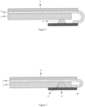
- the flexible display screen may comprise a display device 11, a flexible substrate 12, a support structure 13, and a drive chip 14, wherein the display device 11 is positioned on the flexible substrate 12, the flexible substrate 12 is positioned on the support structure 13, and the drive chip 14 is positioned below the support structure 13, and wherein the support structure 13 is used to support the flexible substrate 12, and the drive chip 14 is used to provide drive for the flexible display screen.
- the display device 11 may emit light under the driving action of the drive chip 14, thereby causing the flexible display screen to emit light.
- the drive chip 14 causes the flexible substrate 12 above it to bend so that the entire screen body is bent, thereby further affecting the display effect of the flexible display screen.
- WO2014/119972A1 discloses an electronic device with flexible display, which can significantly reduce the non-display area of a flexible OLED display, which would otherwise be covered by a cosmetic trim such as a bezel or an opaque. As such, an electronic device with a display having minimized border area can be provided. This makes it possible to reduce the overall size of the electronic device without sacrificing the size of the display therein. Such a reduction in size of the bezel was achieved by bending the flexible substrate near its edge using an insert member.
- EP2827372A2 discloses a flexible display device.
- the flexible display device includes a display panel including a plastic substrate where an organic light emitting diode and a thin film transistor are formed; a circuit portion applying a power signal and a data signal, which are supplied from an external portion, to the display panel; and a support member coupled to the plastic substrate, wherein the display panel and the circuit portion are bent around the support member.
- the main object of the disclosure is to provide a flexible display screen and a flexible display apparatus, which aim to solve the problem in the prior art that the drive chip causes the screen body to bend due to having a certain thickness, , thereby further affecting the display effect of the flexible display screen.
- a thickness of the support structure is equal to or larger than a thickness of the drive chip.
- a shape and a position of the groove match a shape and a position of the drive chip.
- the display device in the flexible display screen is an OLED.
- the flexible display screen further comprises a first film, a second film and a connecting member, wherein the first film is positioned on the display device, the connecting member is positioned on the first film and the second film is positioned on the connecting member.
- the disclosure provides a flexible display apparatus comprising the above flexible display screen.
- the flexible display screen comprises a display device, a flexible substrate, a support structure and a drive chip, the display device is positioned on the flexible substrate, and the flexible substrate is positioned on the support structure, wherein the support structure is provided with a groove which is used to the drive chip.
- the groove for receiving the drive chip is disposed in the support structure of the flexible display screen in comparison with the prior art, the drive chip does not bend the screen body of the flexible display screen, thereby further not affecting the display effect of the flexible display screen.
- first”, “second”, and the like in the disclosure are only used for descriptive purposes, and should not be construed as indicating or implying their relative importance or implicitly indicating the number of technical features indicated.
- features defined with “first” or “second” may comprise at least one of the features, either explicitly or implicitly.
- the meaning of "a plurality of” is at least two, such as two, three, etc., unless otherwise expressly and specifically defined.
- fixed may be a fixed connection, or may be a detachable connection, or may be integrated; may be mechanically connected or electrically connected; may be directly connected, or may be indirectly connected through an intermediate medium; may be internal communication of two elements or an interaction relationship of two elements, unless otherwise explicitly defined.
- fixed may be a fixed connection, or may be a detachable connection, or may be integrated; may be mechanically connected or electrically connected; may be directly connected, or may be indirectly connected through an intermediate medium; may be internal communication of two elements or an interaction relationship of two elements, unless otherwise explicitly defined.
- the flexible display screen in the embodiments of the disclosure refers to a display screen in which an ineffective display area is bent.
- the technical solutions provided by the embodiments of the disclosure may ensure that the drive chip in the flexible display screen would not cause screen body to bend and then the display effect of the flexible display screen would not be affected .
- a support block and a double-sided tape are usually bound on the outside of the support structure, which may avoid the drive chip from protruding against the screen body and allows the screen body not to bend or affect the display effect of the flexible display screen.
- binding the support block and double-sided tape makes the manufacturing process of the flexible display screen more complicated and the manufacturing cost higher, and considering the expansion rate of materials, the expansion ratio of the selected materials for the support block and double-sided tape is required to be suitable for the support structure so that it is hard to select materials. Once there is a problem of the material selection, the corresponding effect will not be achieved.
- the flexible display screen provided by the embodiments of the disclosure may not only cause the screen body not to bend, thereby not affecting the display effect, but also reduce the manufacturing cost and simplify the manufacturing process and avoid the problem of difficult material selection.
- the support structure in the flexible display screen in the embodiments of the disclosure does not affect the display effect of the flexible display screen, the support structure would not affect the display effect of the flexible display screen after a groove is disposed in the support structure in the flexible display screen.
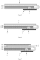
- FIG. 2 is a structural schematic view of a flexible display screen provided by an embodiment not forming part of the claimed invention.
- the flexible display screen is described as follows.
- the flexible display screen includes a display device 21, a flexible substrate 22, a support structure 23, and a drive chip 24, wherein the display device 21 is positioned on the flexible substrate 22 and the flexible substrate 22 is positioned on the support structure 23. That is to say, the display device 21, the flexible substrate 22, and the support structure 23 included in the flexible display screen provided by the embodiment of the disclosure are sequentially connected from top to bottom in the order of the display device 21, the flexible substrate 22, and the support structure 23.
- the drive chip 24 may be positioned on a flexible circuit board.
- a groove 25 is disposed in the support structure 23 and may be used to receive the drive chip 24 in the flexible display screen. As shown in FIG. 2 , the drive chip 24 is positioned within the groove 25. Thus, the drive chip 24 does not protrude against the upper flexible substrate 22 in comparison with the prior art so that the screen body of the flexible display screen is not bent, and thus does not affect display effect of the flexible display screen.
- the thickness of the support structure 23 it is necessary to make the thickness of the support structure 23 be greater than or equal to the thickness of the drive chip 24 so that the groove 25 disposed in the support structure 23 may receive the drive chip 24.
- the thickness of the support structure 23 in the flexible display screen is smaller than the thickness of the drive chip 24, the thickness of the support structure 23 may be increased when designing the support structure 23, so that the groove 25 disposed in the support structure 23 may receive the drive chip 24.
- the shape and position of the groove 25 may be determined according to the shape and position of the drive chip 24 when disposing the groove 25 in the support structure 23 .
- the drive chip 24 has a trapezoidal cross section, so the cross section of the groove 25 may also be trapezoidal and the height of the trapezoid may be determined according to the thickness of the drive chip 24, so as to receive the drive chip 24. For example, if the drive chip 24 has a thickness of 0.2 mm, the groove 25 having a height of greater than 0.2 mm is required to receive the drive chip 24.
- FIG. 3 it is a top view of the groove 25.
- the drive chip 24 has a shape of rectangle, so the groove 25 has also a shape of rectangle from the top view, and the rectangular length from the top view of the groove 25 may be determined according to the rectangular length from the top view of the drive chip 24, and the width may be determined according to the rectangular width from the top view of the drive chip 24, so that the groove 25 can receive the drive chip 24.
- the drive chip 24 has a shape of rectangle from the top view, and the length of the rectangle is 0.3 mm and the width is 0.2 mm, so the rectangular length from the top view of the groove 25 is required to be greater than 0.3 mm, and the width is required to be greater than 0.2 mm.
- the support structure 23 may serve to support the flexible substrate 22, and the support structure 23 can be a support film.
- the display device 21 may be an OLED, or may be an LED, and may also be other display devices, which is not specifically defined herein. As a preferred manner, the display device 21 is an OLED.
- the material for the flexible substrate 22 may be a PI (its English full name: Polyimide) material.
- the flexible display screen provided by the embodiment of the disclosure includes a display device, a flexible substrate, a support structure and a drive chip, and the display device is positioned on the flexible substrate and the flexible substrate is positioned on the support structure, wherein the support structure is provided with a groove for receiving the drive chip.
- the drive chip since the groove for receiving the drive chip has been disposed in the support structure of the flexible display screen in comparison with the prior art, the drive chip would not bend the screen body of the flexible display screen, thereby not affecting the display effect of the flexible display screen.
- FIG. 4 is a structural schematic view of another flexible display screen provided by an embodiment not forming part of the claimed invention.
- the flexible display screen is described as follows.
- the flexible display screen includes the display device 21, the flexible substrate 22, a support film 231, a cushioning member 232, and the drive chip 24.
- the display device 21, the flexible substrate 22, the support film 231 and the cushioning member 232 are sequentially connected from top to bottom in the order of the display device 21, the flexible substrate 22, the support film 231, and the cushioning member 232.
- the support film 231 and the cushioning member 232 jointly constitute the support member 23 described in the embodiment 1, and the total thicknesses of the support film 231 and the cushioning member 232 is greater than or equal to the thickness of the drive chip 24.
- the cushioning member 232 serves to cushion the flexible display screen, and the cushioning member 232 may be a foam.
- the groove 25 may be disposed in the cushioning member 232.
- the groove 25 may also be disposed in the support film 231 and the cushioning member 232.
- the groove 25 is used to receive the drive chip 24 in the flexible display screen.
- the groove 25 may be disposed in the cushioning member 232, or alternatively may be disposed in the support film 231 and the cushioning member 232; if the thickness of the cushioning member 232 is smaller than the thickness of the drive chip 24 and the thickness of the support film 231 and the cushioning member 232 is greater than the thickness of the drive chip 24, then, the groove 25 may be disposed in the support film 231 and the cushioning member 232.
- the groove 25 having a thickness of 0.28 mm may be disposed only in the cushioning member 232, and the groove 25 having a thickness of 0.40 mm may be disposed in the cushioning member 232 and the support film 231 to receive the drive chip 24;
- the drive chip 24 has a thickness of 0.25 mm
- the cushioning member 232 has a thickness of 0.10 mm and the support film 231 has a thickness of 0.20 mm
- the groove 25 having a thickness of 0.28 mm may be disposed in the cushioning member 232 and the support film 231 to receive the drive chip 24.
- the drive chip 24 is positioned in the groove 25, and the groove 25 is disposed in the cushioning member 232 and the support film 231.
- the flexible display screen provided by the embodiment of the disclosure includes a display device, a flexible substrate, a support film, a cushioning member, and a drive chip, and the display device is positioned on the flexible substrate and the flexible substrate is positioned on the support film, and the support film is positioned in the cushioning member, wherein a groove is disposed in the support film and/or the cushioning member and is used to receive the drive chip.
- the drive chip since the groove for receiving the drive chip has been disposed in the support film and/or the cushioning member of the flexible display screen in comparison with the prior art, the drive chip would not protrude against the flexible substrate, thereby not bending the screen body of the flexible display screen, and further not affecting the display effect of the flexible display screen.
- FIG. 5 is a structural schematic view of another flexible display screen provided by an embodiment not forming part of the claimed invention.
- the flexible display screen is described as follows.
- the flexible display screen includes the display device 21, the flexible substrate 22, the support film 231, a heat-dissipating member 233, and the drive chip 24.
- the display device 21, the flexible substrate 22, the support film 231 and the heat-dissipating member 233 are sequentially connected from top to bottom in the order of the display device 21, the flexible substrate 22, the support film 231 and the heat-dissipating member 233.
- the support film 231 and the heat-dissipating member 233 jointly constitute the support member 23 described in the embodiment 1, and the total thicknesses of the support film 231 and the heat-dissipating member 233 is greater than or equal to the thickness of the drive chip 24, wherein the heat-dissipating member 233 serves to dissipate heat from the flexible display screen, and the heat-dissipating member 233 may be a copper foil.
- the groove 25 may be disposed in the heat-dissipating member 233.
- the groove 25 may be disposed in the support film 231 and the heat-dissipating member 233.
- the groove 25 is used to receive the drive chip 24 in the flexible display screen.
- the groove 25 may be disposed only in the heat-dissipating member 233, or alternatively the groove 25 may be disposed in the heat-dissipating member 233 and the support film 231; if the thickness of the heat-dissipating member 233 is smaller than the thickness of the drive chip 24 and the thickness of the heat-dissipating member 233 and the support film 231 is greater than the drive chip 24, the groove 25 may be disposed in the heat-dissipating member 233 and the support film 231.
- the groove 25 having a thickness of 0.25 mm may be disposed only in the heat-dissipating member 233, or the groove 25 having a thickness of 0.30 mm may be disposed in the heat-dissipating member 233 and the support film 231 for receiving the drive chip 24; if the drive chip 24 has a thickness of 0.20 mm, the heat-dissipating member 233 has a thickness of 0.10 mm and the support film 231 has a thickness of 0.20 mm, the groove 25 having a thickness of 0.25 mm may be disposed in the heat-dissipating member 233 and the support film 231 for receiving the drive chip 24.
- the drive chip 24 is positioned within the groove 25, and the groove 25 is positioned in the heat-dissipating member 233 and the support film 231.
- the flexible display screen provided by the embodiment of the disclosure includes a display device, a flexible substrate, a support film, a heat-dissipating member and a drive chip.
- the display device is positioned on the flexible substrate, the flexible substrate is positioned on the support film, and the support film is positioned on the heat-dissipating member, wherein a groove is disposed in the support film and/or the heat-dissipating member and serves to receive the drive chip.
- the embodiment of the disclosure provides the groove for receiving the drive chip in the support film and/or the heat-dissipating member of the flexible display screen in comparison with the prior art, the drive chip does not protrude against the flexible substrate, thereby not bending the screen body of the flexible display screen and further not affecting the display effect of the flexible display screen.
- FIG. 6 is a structural schematic view of still another flexible display screen provided by an embodiment in accordance with the claimed invention.
- the flexible display screen is described as follows.
- the flexible display screen includes the display device 21, the flexible substrate 22, the support film 231, the cushioning member 232, the heat-dissipating member 233, and the drive chip 24.
- the display device 21, the flexible substrate 22, the support film 231, the cushioning member 232, and the heat-dissipating member 233 are sequentially connected from top to bottom in the order of the display device 21, the flexible substrate 22, the support film 231, the cushioning member 232 and the heat-dissipating member 233.
- the support film 231, the cushioning member 232, and the heat-dissipating member 233 jointly constitute the support member 23 described in the embodiment 1.
- the total thickness of the support film 231, the cushioning member 232 and the heat-dissipating members 233 is greater than or equal to the thickness of the drive chip 24.
- the cushioning member 232 serves to cushion the flexible display screen, and the heat-dissipating component 233 serves to dissipate heat from the flexible display screen.
- the cushioning member 232 is a foam.
- the heat-dissipating member 233 is a copper foil.
- the groove 25 is disposed in the heat-dissipating member 233, the cushioning member 232 and the support film 231.
- the groove 25 serves to receive the drive chip 24 in the flexible display screen.
- the groove 25 may be disposed in the heat-dissipating member 233, the cushioning member 232 and the support film 231 and the disposed groove 25 can have a thickness of 0.28 mm.
- the drive chip 24 is positioned in the groove 25, and the groove 25 is disposed in the support film 231, the cushioning member 232 and the heat-dissipating member 233.
- the flexible display screen includes a display device, a flexible substrate, a support film, a cushioning member, a heat-dissipating member and a drive chip.
- the display device is positioned on the flexible substrate, the flexible substrate is positioned on the support film, the support film is positioned on the cushioning member and the cushioning member is positioned on the heat-dissipating member, wherein a groove is disposed in the support film, the cushioning member and/or the heat-dissipating member for receiving the drive chip.
- the drive chip since the groove for receiving the drive chip has been disposed in the support film, the cushioning member and the heat-dissipating member of the flexible display screen in comparison with the prior art, the drive chip does not protrude against the flexible substrate, thereby not bending the screen body of the flexible display screen, and further not affecting the display effect of the flexible display screen.
- FIG. 7 is a structural schematic view of still another flexible display screen provided by an embodiment in accordance with the claimed invention.
- the flexible display screen is described as follows.
- the flexible display screen shown in FIG. 7 is different from the flexible display screen shown in FIG. 6 in that a first film 26, a connecting member 27, and a second film 28 are sequentially added on the display device 21 of the flexible display screen in FIG. 7 .
- the first film 26 provides a first layer of protection for the display device 21, and the second film 28 provides a second layer of protection for the display device 21, and the connecting member 27 serves to connect the first film 26 with the second film 28 and may be a gel-like material.
- the flexible display screen provided by the embodiment of the disclosure includes a second film, a connecting member, a first film, a display device, a flexible substrate, a support film, a cushioning member and a heat-dissipating member which are sequentially connected one another, wherein a groove is disposed in the support film, the cushioning member, and the heat-dissipating member for receiving a drive chip.
- the drive chip does not protrude against the flexible substrate, and correspondingly the screen body of the flexible display screen would not bend, thereby not affecting the display effect of the flexible display screen.
- Embodiments of the disclosure further provide a flexible display apparatus comprising the above flexible display screen.
Landscapes
- Engineering & Computer Science (AREA)
- Physics & Mathematics (AREA)
- Theoretical Computer Science (AREA)
- General Physics & Mathematics (AREA)
- Nonlinear Science (AREA)
- Computer Hardware Design (AREA)
- Devices For Indicating Variable Information By Combining Individual Elements (AREA)
- Mathematical Physics (AREA)
- Crystallography & Structural Chemistry (AREA)
- Optics & Photonics (AREA)
- Chemical & Material Sciences (AREA)
- Human Computer Interaction (AREA)
- General Engineering & Computer Science (AREA)
- Microelectronics & Electronic Packaging (AREA)
- Thermal Sciences (AREA)
- Electroluminescent Light Sources (AREA)
Applications Claiming Priority (2)
| Application Number | Priority Date | Filing Date | Title |
|---|---|---|---|
| CN201710149699.1A CN108573656A (zh) | 2017-03-14 | 2017-03-14 | 一种柔性显示屏以及柔性显示装置 |
| PCT/CN2018/078365 WO2018166390A1 (zh) | 2017-03-14 | 2018-03-08 | 一种柔性显示屏以及柔性显示装置 |
Publications (3)
| Publication Number | Publication Date |
|---|---|
| EP3550543A1 EP3550543A1 (en) | 2019-10-09 |
| EP3550543A4 EP3550543A4 (en) | 2020-01-15 |
| EP3550543B1 true EP3550543B1 (en) | 2024-12-04 |
Family
ID=63522789
Family Applications (1)
| Application Number | Title | Priority Date | Filing Date |
|---|---|---|---|
| EP18766966.8A Active EP3550543B1 (en) | 2017-03-14 | 2018-03-08 | Flexible display screen and flexible display apparatus |
Country Status (7)
| Country | Link |
|---|---|
| US (1) | US11233208B2 (enExample) |
| EP (1) | EP3550543B1 (enExample) |
| JP (1) | JP6895523B2 (enExample) |
| KR (1) | KR102272886B1 (enExample) |
| CN (1) | CN108573656A (enExample) |
| TW (1) | TW201834237A (enExample) |
| WO (1) | WO2018166390A1 (enExample) |
Families Citing this family (39)
| Publication number | Priority date | Publication date | Assignee | Title |
|---|---|---|---|---|
| KR102018741B1 (ko) * | 2013-06-03 | 2019-09-06 | 삼성디스플레이 주식회사 | 커버 윈도우를 구비하는 표시 장치 |
| CN109699151B (zh) * | 2017-10-20 | 2020-02-14 | 华为技术有限公司 | 膜状散热构件、可折弯显示装置以及终端设备 |
| CN109375408A (zh) * | 2018-12-17 | 2019-02-22 | 武汉华星光电半导体显示技术有限公司 | 一种柔性显示装置 |
| CN115485755B (zh) * | 2019-03-05 | 2025-03-21 | 京东方科技集团股份有限公司 | 一种柔性屏 |
| CN110164874B (zh) * | 2019-06-04 | 2021-06-22 | 上海天马微电子有限公司 | 柔性显示模组、显示装置及柔性显示模组的制作方法 |
| CN110233918B (zh) * | 2019-06-18 | 2024-06-11 | 陈健 | 一种折叠屏、折叠屏展开装置以及终端 |
| CN112153176B (zh) * | 2019-06-27 | 2021-08-13 | Oppo广东移动通信有限公司 | 电子设备 |
| KR102798328B1 (ko) * | 2019-08-19 | 2025-04-23 | 삼성디스플레이 주식회사 | 전자 모듈 및 전자 모듈 제조 방법 |
| CN110503898A (zh) * | 2019-08-28 | 2019-11-26 | 京东方科技集团股份有限公司 | 微发光二极管显示面板及制备方法、拼接显示面板、装置 |
| CN110767092B (zh) * | 2019-11-05 | 2021-11-23 | 京东方科技集团股份有限公司 | 显示装置 |
| WO2021088037A1 (zh) * | 2019-11-08 | 2021-05-14 | 京东方科技集团股份有限公司 | 阵列基板及其制造方法、显示面板、显示装置 |
| CN110828530A (zh) * | 2019-11-28 | 2020-02-21 | 武汉华星光电半导体显示技术有限公司 | 一种显示面板及其制备方法、显示装置 |
| KR102787589B1 (ko) * | 2020-02-18 | 2025-03-28 | 삼성디스플레이 주식회사 | 표시 장치 |
| CN111261047A (zh) * | 2020-02-27 | 2020-06-09 | 昆山国显光电有限公司 | 一种显示面板及显示装置 |
| KR102801361B1 (ko) * | 2020-03-16 | 2025-05-02 | 삼성디스플레이 주식회사 | 표시장치 |
| CN111402728B (zh) * | 2020-03-24 | 2022-05-31 | 京东方科技集团股份有限公司 | 弯折垫片组件、柔性oled模组以及oled设备 |
| KR102772815B1 (ko) * | 2020-04-29 | 2025-02-27 | 삼성전자주식회사 | 방열 시트를 포함하는 전자 장치 |
| US11889647B2 (en) * | 2020-08-19 | 2024-01-30 | Apple Inc. | Display panel bend reinforcement |
| US11723180B2 (en) * | 2020-09-07 | 2023-08-08 | Chengdu Boe Optoelectronics Technology Co., Ltd. | Display module and method for manufacturing same, and display device |
| CN116235235A (zh) | 2020-11-06 | 2023-06-06 | 三星电子株式会社 | 包括散热构件的电子设备 |
| KR102836941B1 (ko) | 2020-12-24 | 2025-07-21 | 엘지디스플레이 주식회사 | 표시 모듈 및 표시 장치 |
| KR102827510B1 (ko) | 2020-12-24 | 2025-06-30 | 엘지디스플레이 주식회사 | 표시 모듈 및 표시 장치 |
| KR102819738B1 (ko) * | 2020-12-24 | 2025-06-11 | 엘지디스플레이 주식회사 | 표시 모듈 및 표시 장치 |
| CN112599019B (zh) * | 2021-01-05 | 2023-01-10 | 武汉华星光电半导体显示技术有限公司 | 显示装置 |
| CN113097271A (zh) * | 2021-03-30 | 2021-07-09 | 合肥维信诺科技有限公司 | 显示装置 |
| CN113516924B (zh) * | 2021-05-19 | 2024-03-26 | 京东方科技集团股份有限公司 | 一种显示模组及电子设备 |
| CN113450651B (zh) * | 2021-06-29 | 2022-10-11 | 上海天马微电子有限公司 | 柔性显示面板散热装置及其应用方法和显示装置 |
| CN118119133A (zh) | 2021-08-02 | 2024-05-31 | 荣耀终端有限公司 | 一种电子设备 |
| CN113763831B (zh) * | 2021-09-16 | 2023-06-20 | 合肥维信诺科技有限公司 | 显示模组及显示装置 |
| CN115019636B (zh) * | 2021-10-26 | 2023-08-15 | 荣耀终端有限公司 | 柔性显示模组以及电子设备 |
| CN114144038B (zh) * | 2021-12-01 | 2025-03-28 | 京东方科技集团股份有限公司 | 一种显示模组及显示装置 |
| CN116931319A (zh) | 2022-03-31 | 2023-10-24 | 京东方科技集团股份有限公司 | 背光模组、显示模组和显示装置 |
| CN117176842A (zh) * | 2022-05-25 | 2023-12-05 | 荣耀终端有限公司 | 电子设备 |
| WO2024000321A1 (zh) * | 2022-06-29 | 2024-01-04 | 京东方科技集团股份有限公司 | 显示模组及显示装置 |
| KR20240107492A (ko) * | 2022-12-30 | 2024-07-09 | 엘지디스플레이 주식회사 | 폴더블 표시 장치 |
| CN116153202B (zh) * | 2023-02-28 | 2025-09-05 | 京东方科技集团股份有限公司 | 一种副屏结构及显示装置 |
| CN116229845B (zh) * | 2023-03-07 | 2026-04-03 | 京东方科技集团股份有限公司 | 显示模组及显示装置 |
| CN121415682A (zh) * | 2024-07-25 | 2026-01-27 | 华为技术有限公司 | 显示屏、显示模组以及电子设备 |
| CN119889170A (zh) * | 2025-02-26 | 2025-04-25 | 京东方科技集团股份有限公司 | 柔性屏幕模组和显示装置 |
Citations (1)
| Publication number | Priority date | Publication date | Assignee | Title |
|---|---|---|---|---|
| KR20140108826A (ko) * | 2013-02-28 | 2014-09-15 | 엘지디스플레이 주식회사 | 플렉서블 디스플레이 장치 및 그 제조 방법 |
Family Cites Families (21)
| Publication number | Priority date | Publication date | Assignee | Title |
|---|---|---|---|---|
| JPS5351970A (en) * | 1976-10-21 | 1978-05-11 | Toshiba Corp | Manufacture for semiconductor substrate |
| JPS6413523A (en) * | 1987-07-08 | 1989-01-18 | Ricoh Kk | Liquid crystal display device |
| KR100942554B1 (ko) | 2008-02-21 | 2010-02-12 | 삼성모바일디스플레이주식회사 | 평판표시장치 |
| US8450838B2 (en) | 2009-08-11 | 2013-05-28 | Seiko Epson Corporation | Electro-optic apparatus, electronic device, and method for manufacturing electro-optic apparatus |
| JP5407649B2 (ja) * | 2009-08-11 | 2014-02-05 | セイコーエプソン株式会社 | 電気光学装置およびその製造方法、電子機器 |
| CN202230276U (zh) * | 2011-06-17 | 2012-05-23 | 北京京东方光电科技有限公司 | 一种液晶显示器及其背光源 |
| KR101190630B1 (ko) * | 2012-01-30 | 2012-10-15 | 주식회사 지앤씨에스 | 유기 발광 표시 장치 |
| KR101985223B1 (ko) * | 2012-11-13 | 2019-06-03 | 엘지디스플레이 주식회사 | 플렉서블 표시장치 |
| US9349969B2 (en) * | 2013-02-01 | 2016-05-24 | Lg Display Co., Ltd. | Electronic devices with flexible display and method for manufacturing the same |
| KR101796813B1 (ko) * | 2013-02-01 | 2017-11-10 | 엘지디스플레이 주식회사 | 플렉서블 유기 발광 표시 장치 및 플렉서블 유기 발광 표시 장치의 제조 방법 |
| KR102046864B1 (ko) * | 2013-03-13 | 2019-11-20 | 삼성전자주식회사 | 유연성 디스플레이 장치 |
| KR102081650B1 (ko) * | 2013-04-10 | 2020-02-26 | 엘지디스플레이 주식회사 | 플렉서블 디스플레이 장치 및 그 제조 방법 |
| KR102089246B1 (ko) * | 2013-07-19 | 2020-03-16 | 엘지디스플레이 주식회사 | 플렉서블 디스플레이 장치 및 플렉서블 디스플레이 장치의 제조방법 |
| CN204189792U (zh) * | 2014-10-22 | 2015-03-04 | 昆山工研院新型平板显示技术中心有限公司 | 显示设备的连接结构和阵列结构 |
| CN204144262U (zh) * | 2014-10-29 | 2015-02-04 | 昆山工研院新型平板显示技术中心有限公司 | 一种散热性良好的柔性显示器 |
| CN106157821A (zh) * | 2015-04-03 | 2016-11-23 | 昆山工研院新型平板显示技术中心有限公司 | 一种柔性显示器件 |
| CN204464289U (zh) * | 2015-04-03 | 2015-07-08 | 昆山工研院新型平板显示技术中心有限公司 | 一种柔性显示结构 |
| KR101905245B1 (ko) * | 2015-07-31 | 2018-10-05 | 삼성에스디아이 주식회사 | 윈도우 필름 및 이를 포함하는 플렉시블 디스플레이 장치 |
| CN204884440U (zh) * | 2015-08-27 | 2015-12-16 | 京东方科技集团股份有限公司 | 柔性显示面板和柔性显示装置 |
| CN205303466U (zh) * | 2016-01-15 | 2016-06-08 | 京东方科技集团股份有限公司 | 一种柔性显示基板、显示装置 |
| CN106356472A (zh) * | 2016-10-18 | 2017-01-25 | 武汉华星光电技术有限公司 | Oled器件制作方法及oled器件 |
-
2017
- 2017-03-14 CN CN201710149699.1A patent/CN108573656A/zh active Pending
-
2018
- 2018-03-08 WO PCT/CN2018/078365 patent/WO2018166390A1/zh not_active Ceased
- 2018-03-08 EP EP18766966.8A patent/EP3550543B1/en active Active
- 2018-03-08 KR KR1020197019409A patent/KR102272886B1/ko active Active
- 2018-03-08 JP JP2019536482A patent/JP6895523B2/ja active Active
- 2018-03-08 US US16/323,433 patent/US11233208B2/en active Active
- 2018-03-14 TW TW107108662A patent/TW201834237A/zh unknown
Patent Citations (1)
| Publication number | Priority date | Publication date | Assignee | Title |
|---|---|---|---|---|
| KR20140108826A (ko) * | 2013-02-28 | 2014-09-15 | 엘지디스플레이 주식회사 | 플렉서블 디스플레이 장치 및 그 제조 방법 |
Also Published As
| Publication number | Publication date |
|---|---|
| EP3550543A4 (en) | 2020-01-15 |
| WO2018166390A1 (zh) | 2018-09-20 |
| KR102272886B1 (ko) | 2021-07-05 |
| US11233208B2 (en) | 2022-01-25 |
| TW201834237A (zh) | 2018-09-16 |
| EP3550543A1 (en) | 2019-10-09 |
| JP2020504844A (ja) | 2020-02-13 |
| US20190393433A1 (en) | 2019-12-26 |
| KR20190087631A (ko) | 2019-07-24 |
| CN108573656A (zh) | 2018-09-25 |
| JP6895523B2 (ja) | 2021-06-30 |
Similar Documents
| Publication | Publication Date | Title |
|---|---|---|
| EP3550543B1 (en) | Flexible display screen and flexible display apparatus | |
| US10910410B2 (en) | Flexible array substrate, flexible display device and method of assembling the same | |
| US10912197B2 (en) | Display device | |
| CN114783299B (zh) | 柔性显示模块以及包括该柔性显示模块的电子装置 | |
| US11706872B2 (en) | Flexible display module and manufacturing method thereof | |
| EP2778773B1 (en) | Flexible display device | |
| US11129281B2 (en) | Flexible circuit film and electronic device comprising the same | |
| EP3295243B1 (en) | Flexible array substrate, display panel having the same, keyboard assembly, and electronic device thereof | |
| KR101881389B1 (ko) | 터치스크린, 그의 제조 방법 및 그를 구비하는 휴대 단말기 | |
| US20200152895A1 (en) | Display panels and methods for manufacturing the same | |
| CN111328193B (zh) | 柔性印刷电路板、柔性显示模块和电子设备 | |
| CN110444678A (zh) | 显示装置和用于显示装置的支撑膜结构 | |
| KR20200073086A (ko) | 플렉서블 디스플레이 모듈 및 이를 포함하는 전자 기기 | |
| EP4089504A1 (en) | Flexible display panel and display apparatus including the flexible display panel | |
| US10734469B2 (en) | Display device | |
| US20210104594A1 (en) | Display panel, preparation method thereof and display device | |
| US20210210568A1 (en) | Substrate, display panel and display device | |
| US11271063B2 (en) | Flexible display structure and electronic device | |
| US20200274105A1 (en) | Display device | |
| KR102034058B1 (ko) | 표시장치 | |
| CN109791744B (zh) | 柔性显示屏和显示装置 | |
| JP2018066993A (ja) | 液晶表示装置およびledアセンブリ | |
| US11778745B2 (en) | Flexible circuit board and display device including the same | |
| KR102124041B1 (ko) | 가요성 표시 패널 및 상기 가요성 표시 패널을 포함하는 표시 장치 | |
| CN108933848B (zh) | 一种显示装置 |
Legal Events
| Date | Code | Title | Description |
|---|---|---|---|
| STAA | Information on the status of an ep patent application or granted ep patent |
Free format text: STATUS: THE INTERNATIONAL PUBLICATION HAS BEEN MADE |
|
| PUAI | Public reference made under article 153(3) epc to a published international application that has entered the european phase |
Free format text: ORIGINAL CODE: 0009012 |
|
| STAA | Information on the status of an ep patent application or granted ep patent |
Free format text: STATUS: REQUEST FOR EXAMINATION WAS MADE |
|
| 17P | Request for examination filed |
Effective date: 20190704 |
|
| AK | Designated contracting states |
Kind code of ref document: A1 Designated state(s): AL AT BE BG CH CY CZ DE DK EE ES FI FR GB GR HR HU IE IS IT LI LT LU LV MC MK MT NL NO PL PT RO RS SE SI SK SM TR |
|
| AX | Request for extension of the european patent |
Extension state: BA ME |
|
| A4 | Supplementary search report drawn up and despatched |
Effective date: 20191216 |
|
| RIC1 | Information provided on ipc code assigned before grant |
Ipc: H01L 27/32 20060101ALI20191210BHEP Ipc: G09F 9/30 20060101AFI20191210BHEP Ipc: H01L 51/50 20060101ALI20191210BHEP |
|
| DAV | Request for validation of the european patent (deleted) | ||
| DAX | Request for extension of the european patent (deleted) | ||
| STAA | Information on the status of an ep patent application or granted ep patent |
Free format text: STATUS: EXAMINATION IS IN PROGRESS |
|
| 17Q | First examination report despatched |
Effective date: 20211209 |
|
| REG | Reference to a national code |
Ref country code: DE Ref legal event code: R079 Free format text: PREVIOUS MAIN CLASS: G09F0009300000 Ipc: H10K0059800000 Ref country code: DE Ref legal event code: R079 Ref document number: 602018077235 Country of ref document: DE Free format text: PREVIOUS MAIN CLASS: G09F0009300000 Ipc: H10K0059800000 |
|
| GRAP | Despatch of communication of intention to grant a patent |
Free format text: ORIGINAL CODE: EPIDOSNIGR1 |
|
| STAA | Information on the status of an ep patent application or granted ep patent |
Free format text: STATUS: GRANT OF PATENT IS INTENDED |
|
| RIC1 | Information provided on ipc code assigned before grant |
Ipc: G09F 9/30 20060101ALI20240607BHEP Ipc: H10K 77/10 20230101ALI20240607BHEP Ipc: H10K 59/80 20230101AFI20240607BHEP |
|
| INTG | Intention to grant announced |
Effective date: 20240709 |
|
| GRAS | Grant fee paid |
Free format text: ORIGINAL CODE: EPIDOSNIGR3 |
|
| GRAA | (expected) grant |
Free format text: ORIGINAL CODE: 0009210 |
|
| STAA | Information on the status of an ep patent application or granted ep patent |
Free format text: STATUS: THE PATENT HAS BEEN GRANTED |
|
| AK | Designated contracting states |
Kind code of ref document: B1 Designated state(s): AL AT BE BG CH CY CZ DE DK EE ES FI FR GB GR HR HU IE IS IT LI LT LU LV MC MK MT NL NO PL PT RO RS SE SI SK SM TR |
|
| REG | Reference to a national code |
Ref country code: GB Ref legal event code: FG4D |
|
| REG | Reference to a national code |
Ref country code: CH Ref legal event code: EP |
|
| REG | Reference to a national code |
Ref country code: DE Ref legal event code: R096 Ref document number: 602018077235 Country of ref document: DE |
|
| REG | Reference to a national code |
Ref country code: IE Ref legal event code: FG4D |
|
| REG | Reference to a national code |
Ref country code: LT Ref legal event code: MG9D |
|
| REG | Reference to a national code |
Ref country code: NL Ref legal event code: MP Effective date: 20241204 |
|
| PG25 | Lapsed in a contracting state [announced via postgrant information from national office to epo] |
Ref country code: HR Free format text: LAPSE BECAUSE OF FAILURE TO SUBMIT A TRANSLATION OF THE DESCRIPTION OR TO PAY THE FEE WITHIN THE PRESCRIBED TIME-LIMIT Effective date: 20241204 |
|
| PG25 | Lapsed in a contracting state [announced via postgrant information from national office to epo] |
Ref country code: FI Free format text: LAPSE BECAUSE OF FAILURE TO SUBMIT A TRANSLATION OF THE DESCRIPTION OR TO PAY THE FEE WITHIN THE PRESCRIBED TIME-LIMIT Effective date: 20241204 |
|
| PG25 | Lapsed in a contracting state [announced via postgrant information from national office to epo] |
Ref country code: BG Free format text: LAPSE BECAUSE OF FAILURE TO SUBMIT A TRANSLATION OF THE DESCRIPTION OR TO PAY THE FEE WITHIN THE PRESCRIBED TIME-LIMIT Effective date: 20241204 |
|
| PG25 | Lapsed in a contracting state [announced via postgrant information from national office to epo] |
Ref country code: ES Free format text: LAPSE BECAUSE OF FAILURE TO SUBMIT A TRANSLATION OF THE DESCRIPTION OR TO PAY THE FEE WITHIN THE PRESCRIBED TIME-LIMIT Effective date: 20241204 |
|
| PG25 | Lapsed in a contracting state [announced via postgrant information from national office to epo] |
Ref country code: NO Free format text: LAPSE BECAUSE OF FAILURE TO SUBMIT A TRANSLATION OF THE DESCRIPTION OR TO PAY THE FEE WITHIN THE PRESCRIBED TIME-LIMIT Effective date: 20250304 |
|
| PG25 | Lapsed in a contracting state [announced via postgrant information from national office to epo] |
Ref country code: LV Free format text: LAPSE BECAUSE OF FAILURE TO SUBMIT A TRANSLATION OF THE DESCRIPTION OR TO PAY THE FEE WITHIN THE PRESCRIBED TIME-LIMIT Effective date: 20241204 Ref country code: GR Free format text: LAPSE BECAUSE OF FAILURE TO SUBMIT A TRANSLATION OF THE DESCRIPTION OR TO PAY THE FEE WITHIN THE PRESCRIBED TIME-LIMIT Effective date: 20250305 |
|
| PG25 | Lapsed in a contracting state [announced via postgrant information from national office to epo] |
Ref country code: RS Free format text: LAPSE BECAUSE OF FAILURE TO SUBMIT A TRANSLATION OF THE DESCRIPTION OR TO PAY THE FEE WITHIN THE PRESCRIBED TIME-LIMIT Effective date: 20250304 |
|
| PG25 | Lapsed in a contracting state [announced via postgrant information from national office to epo] |
Ref country code: NL Free format text: LAPSE BECAUSE OF FAILURE TO SUBMIT A TRANSLATION OF THE DESCRIPTION OR TO PAY THE FEE WITHIN THE PRESCRIBED TIME-LIMIT Effective date: 20241204 |
|
| REG | Reference to a national code |
Ref country code: AT Ref legal event code: MK05 Ref document number: 1749543 Country of ref document: AT Kind code of ref document: T Effective date: 20241204 |
|
| PG25 | Lapsed in a contracting state [announced via postgrant information from national office to epo] |
Ref country code: SM Free format text: LAPSE BECAUSE OF FAILURE TO SUBMIT A TRANSLATION OF THE DESCRIPTION OR TO PAY THE FEE WITHIN THE PRESCRIBED TIME-LIMIT Effective date: 20241204 |
|
| PG25 | Lapsed in a contracting state [announced via postgrant information from national office to epo] |
Ref country code: PL Free format text: LAPSE BECAUSE OF FAILURE TO SUBMIT A TRANSLATION OF THE DESCRIPTION OR TO PAY THE FEE WITHIN THE PRESCRIBED TIME-LIMIT Effective date: 20241204 |
|
| PG25 | Lapsed in a contracting state [announced via postgrant information from national office to epo] |
Ref country code: IS Free format text: LAPSE BECAUSE OF FAILURE TO SUBMIT A TRANSLATION OF THE DESCRIPTION OR TO PAY THE FEE WITHIN THE PRESCRIBED TIME-LIMIT Effective date: 20250404 |
|
| PG25 | Lapsed in a contracting state [announced via postgrant information from national office to epo] |
Ref country code: PT Free format text: LAPSE BECAUSE OF FAILURE TO SUBMIT A TRANSLATION OF THE DESCRIPTION OR TO PAY THE FEE WITHIN THE PRESCRIBED TIME-LIMIT Effective date: 20250404 |
|
| PG25 | Lapsed in a contracting state [announced via postgrant information from national office to epo] |
Ref country code: EE Free format text: LAPSE BECAUSE OF FAILURE TO SUBMIT A TRANSLATION OF THE DESCRIPTION OR TO PAY THE FEE WITHIN THE PRESCRIBED TIME-LIMIT Effective date: 20241204 |
|
| PG25 | Lapsed in a contracting state [announced via postgrant information from national office to epo] |
Ref country code: RO Free format text: LAPSE BECAUSE OF FAILURE TO SUBMIT A TRANSLATION OF THE DESCRIPTION OR TO PAY THE FEE WITHIN THE PRESCRIBED TIME-LIMIT Effective date: 20241204 Ref country code: AT Free format text: LAPSE BECAUSE OF FAILURE TO SUBMIT A TRANSLATION OF THE DESCRIPTION OR TO PAY THE FEE WITHIN THE PRESCRIBED TIME-LIMIT Effective date: 20241204 |
|
| PG25 | Lapsed in a contracting state [announced via postgrant information from national office to epo] |
Ref country code: SK Free format text: LAPSE BECAUSE OF FAILURE TO SUBMIT A TRANSLATION OF THE DESCRIPTION OR TO PAY THE FEE WITHIN THE PRESCRIBED TIME-LIMIT Effective date: 20241204 |
|
| PG25 | Lapsed in a contracting state [announced via postgrant information from national office to epo] |
Ref country code: CZ Free format text: LAPSE BECAUSE OF FAILURE TO SUBMIT A TRANSLATION OF THE DESCRIPTION OR TO PAY THE FEE WITHIN THE PRESCRIBED TIME-LIMIT Effective date: 20241204 |
|
| PG25 | Lapsed in a contracting state [announced via postgrant information from national office to epo] |
Ref country code: IT Free format text: LAPSE BECAUSE OF FAILURE TO SUBMIT A TRANSLATION OF THE DESCRIPTION OR TO PAY THE FEE WITHIN THE PRESCRIBED TIME-LIMIT Effective date: 20241204 |
|
| REG | Reference to a national code |
Ref country code: DE Ref legal event code: R097 Ref document number: 602018077235 Country of ref document: DE |
|
| PG25 | Lapsed in a contracting state [announced via postgrant information from national office to epo] |
Ref country code: SE Free format text: LAPSE BECAUSE OF FAILURE TO SUBMIT A TRANSLATION OF THE DESCRIPTION OR TO PAY THE FEE WITHIN THE PRESCRIBED TIME-LIMIT Effective date: 20241204 |
|
| PG25 | Lapsed in a contracting state [announced via postgrant information from national office to epo] |
Ref country code: DK Free format text: LAPSE BECAUSE OF FAILURE TO SUBMIT A TRANSLATION OF THE DESCRIPTION OR TO PAY THE FEE WITHIN THE PRESCRIBED TIME-LIMIT Effective date: 20241204 |
|
| PLBE | No opposition filed within time limit |
Free format text: ORIGINAL CODE: 0009261 |
|
| STAA | Information on the status of an ep patent application or granted ep patent |
Free format text: STATUS: NO OPPOSITION FILED WITHIN TIME LIMIT |
|
| PG25 | Lapsed in a contracting state [announced via postgrant information from national office to epo] |
Ref country code: MC Free format text: LAPSE BECAUSE OF FAILURE TO SUBMIT A TRANSLATION OF THE DESCRIPTION OR TO PAY THE FEE WITHIN THE PRESCRIBED TIME-LIMIT Effective date: 20241204 |
|
| REG | Reference to a national code |
Ref country code: CH Ref legal event code: L10 Free format text: ST27 STATUS EVENT CODE: U-0-0-L10-L00 (AS PROVIDED BY THE NATIONAL OFFICE) Effective date: 20251015 |
|
| REG | Reference to a national code |
Ref country code: CH Ref legal event code: H13 Free format text: ST27 STATUS EVENT CODE: U-0-0-H10-H13 (AS PROVIDED BY THE NATIONAL OFFICE) Effective date: 20251023 |
|
| 26N | No opposition filed |
Effective date: 20250905 |
|
| PG25 | Lapsed in a contracting state [announced via postgrant information from national office to epo] |
Ref country code: LU Free format text: LAPSE BECAUSE OF NON-PAYMENT OF DUE FEES Effective date: 20250308 |
|
| GBPC | Gb: european patent ceased through non-payment of renewal fee |
Effective date: 20250308 |
|
| REG | Reference to a national code |
Ref country code: BE Ref legal event code: MM Effective date: 20250331 |
|
| PG25 | Lapsed in a contracting state [announced via postgrant information from national office to epo] |
Ref country code: GB Free format text: LAPSE BECAUSE OF NON-PAYMENT OF DUE FEES Effective date: 20250308 |
|
| PG25 | Lapsed in a contracting state [announced via postgrant information from national office to epo] |
Ref country code: FR Free format text: LAPSE BECAUSE OF NON-PAYMENT OF DUE FEES Effective date: 20250331 |
|
| PG25 | Lapsed in a contracting state [announced via postgrant information from national office to epo] |
Ref country code: BE Free format text: LAPSE BECAUSE OF NON-PAYMENT OF DUE FEES Effective date: 20250331 |
|
| PG25 | Lapsed in a contracting state [announced via postgrant information from national office to epo] |
Ref country code: CH Free format text: LAPSE BECAUSE OF NON-PAYMENT OF DUE FEES Effective date: 20250331 |
|
| PG25 | Lapsed in a contracting state [announced via postgrant information from national office to epo] |
Ref country code: IE Free format text: LAPSE BECAUSE OF NON-PAYMENT OF DUE FEES Effective date: 20250308 |
|
| PGFP | Annual fee paid to national office [announced via postgrant information from national office to epo] |
Ref country code: DE Payment date: 20260313 Year of fee payment: 9 |