EP3549159B1 - Transparent film error correction pattern in wafer geometry system - Google Patents
Transparent film error correction pattern in wafer geometry system Download PDFInfo
- Publication number
- EP3549159B1 EP3549159B1 EP18735858.5A EP18735858A EP3549159B1 EP 3549159 B1 EP3549159 B1 EP 3549159B1 EP 18735858 A EP18735858 A EP 18735858A EP 3549159 B1 EP3549159 B1 EP 3549159B1
- Authority
- EP
- European Patent Office
- Prior art keywords
- wafer
- thickness
- correction model
- geometry
- measurement
- Prior art date
- Legal status (The legal status is an assumption and is not a legal conclusion. Google has not performed a legal analysis and makes no representation as to the accuracy of the status listed.)
- Active
Links
Images


Classifications
-
- G—PHYSICS
- G01—MEASURING; TESTING
- G01B—MEASURING LENGTH, THICKNESS OR SIMILAR LINEAR DIMENSIONS; MEASURING ANGLES; MEASURING AREAS; MEASURING IRREGULARITIES OF SURFACES OR CONTOURS
- G01B21/00—Measuring arrangements or details thereof, where the measuring technique is not covered by the other groups of this subclass, unspecified or not relevant
- G01B21/02—Measuring arrangements or details thereof, where the measuring technique is not covered by the other groups of this subclass, unspecified or not relevant for measuring length, width, or thickness
- G01B21/04—Measuring arrangements or details thereof, where the measuring technique is not covered by the other groups of this subclass, unspecified or not relevant for measuring length, width, or thickness by measuring coordinates of points
- G01B21/045—Correction of measurements
-
- H—ELECTRICITY
- H01—ELECTRIC ELEMENTS
- H01L—SEMICONDUCTOR DEVICES NOT COVERED BY CLASS H10
- H01L22/00—Testing or measuring during manufacture or treatment; Reliability measurements, i.e. testing of parts without further processing to modify the parts as such; Structural arrangements therefor
- H01L22/10—Measuring as part of the manufacturing process
- H01L22/12—Measuring as part of the manufacturing process for structural parameters, e.g. thickness, line width, refractive index, temperature, warp, bond strength, defects, optical inspection, electrical measurement of structural dimensions, metallurgic measurement of diffusions
-
- G—PHYSICS
- G01—MEASURING; TESTING
- G01B—MEASURING LENGTH, THICKNESS OR SIMILAR LINEAR DIMENSIONS; MEASURING ANGLES; MEASURING AREAS; MEASURING IRREGULARITIES OF SURFACES OR CONTOURS
- G01B11/00—Measuring arrangements characterised by the use of optical techniques
- G01B11/02—Measuring arrangements characterised by the use of optical techniques for measuring length, width or thickness
- G01B11/06—Measuring arrangements characterised by the use of optical techniques for measuring length, width or thickness for measuring thickness ; e.g. of sheet material
- G01B11/0616—Measuring arrangements characterised by the use of optical techniques for measuring length, width or thickness for measuring thickness ; e.g. of sheet material of coating
- G01B11/0675—Measuring arrangements characterised by the use of optical techniques for measuring length, width or thickness for measuring thickness ; e.g. of sheet material of coating using interferometry
-
- G—PHYSICS
- G01—MEASURING; TESTING
- G01B—MEASURING LENGTH, THICKNESS OR SIMILAR LINEAR DIMENSIONS; MEASURING ANGLES; MEASURING AREAS; MEASURING IRREGULARITIES OF SURFACES OR CONTOURS
- G01B11/00—Measuring arrangements characterised by the use of optical techniques
- G01B11/24—Measuring arrangements characterised by the use of optical techniques for measuring contours or curvatures
- G01B11/2441—Measuring arrangements characterised by the use of optical techniques for measuring contours or curvatures using interferometry
-
- G—PHYSICS
- G01—MEASURING; TESTING
- G01N—INVESTIGATING OR ANALYSING MATERIALS BY DETERMINING THEIR CHEMICAL OR PHYSICAL PROPERTIES
- G01N21/00—Investigating or analysing materials by the use of optical means, i.e. using sub-millimetre waves, infrared, visible or ultraviolet light
- G01N21/84—Systems specially adapted for particular applications
- G01N21/8422—Investigating thin films, e.g. matrix isolation method
-
- G—PHYSICS
- G01—MEASURING; TESTING
- G01N—INVESTIGATING OR ANALYSING MATERIALS BY DETERMINING THEIR CHEMICAL OR PHYSICAL PROPERTIES
- G01N21/00—Investigating or analysing materials by the use of optical means, i.e. using sub-millimetre waves, infrared, visible or ultraviolet light
- G01N21/84—Systems specially adapted for particular applications
- G01N21/88—Investigating the presence of flaws or contamination
- G01N21/95—Investigating the presence of flaws or contamination characterised by the material or shape of the object to be examined
- G01N21/9501—Semiconductor wafers
-
- G—PHYSICS
- G01—MEASURING; TESTING
- G01N—INVESTIGATING OR ANALYSING MATERIALS BY DETERMINING THEIR CHEMICAL OR PHYSICAL PROPERTIES
- G01N21/00—Investigating or analysing materials by the use of optical means, i.e. using sub-millimetre waves, infrared, visible or ultraviolet light
- G01N21/84—Systems specially adapted for particular applications
- G01N21/88—Investigating the presence of flaws or contamination
- G01N21/95—Investigating the presence of flaws or contamination characterised by the material or shape of the object to be examined
- G01N21/956—Inspecting patterns on the surface of objects
-
- H—ELECTRICITY
- H01—ELECTRIC ELEMENTS
- H01L—SEMICONDUCTOR DEVICES NOT COVERED BY CLASS H10
- H01L22/00—Testing or measuring during manufacture or treatment; Reliability measurements, i.e. testing of parts without further processing to modify the parts as such; Structural arrangements therefor
- H01L22/20—Sequence of activities consisting of a plurality of measurements, corrections, marking or sorting steps
- H01L22/24—Optical enhancement of defects or not directly visible states, e.g. selective electrolytic deposition, bubbles in liquids, light emission, colour change
-
- H—ELECTRICITY
- H01—ELECTRIC ELEMENTS
- H01L—SEMICONDUCTOR DEVICES NOT COVERED BY CLASS H10
- H01L22/00—Testing or measuring during manufacture or treatment; Reliability measurements, i.e. testing of parts without further processing to modify the parts as such; Structural arrangements therefor
- H01L22/30—Structural arrangements specially adapted for testing or measuring during manufacture or treatment, or specially adapted for reliability measurements
-
- G—PHYSICS
- G01—MEASURING; TESTING
- G01B—MEASURING LENGTH, THICKNESS OR SIMILAR LINEAR DIMENSIONS; MEASURING ANGLES; MEASURING AREAS; MEASURING IRREGULARITIES OF SURFACES OR CONTOURS
- G01B2210/00—Aspects not specifically covered by any group under G01B, e.g. of wheel alignment, caliper-like sensors
- G01B2210/56—Measuring geometric parameters of semiconductor structures, e.g. profile, critical dimensions or trench depth
Definitions
- the disclosure generally relates to the field of inspection and metrology, and particularly to inspection and metrology of semiconductor devices including transparent films.
- Thin polished plates such as silicon wafers and the like are a very important part of modern technology.
- a wafer for instance, may refer to a thin slice of semiconductor material used in the fabrication of integrated circuits and other devices.
- Other examples of thin polished plates may include magnetic disc substrates, gauge blocks, and the like. While the technique described here refers mainly to wafers, it is to be understood that the technique is also applicable to other types of polished plates as well.
- the term wafer and the term thin polished plate may be used interchangeably in the present disclosure.
- Wafers are subjects to defect inspection as well as metrology measurements to ensure proper fabrication yield. Tools utilized to perform such inspection and metrology processes are expected to be efficient and effective. Key metrics acquired from wafers include, but are not limited to, film thickness and wafer topography. While point-to-point ellipsometer-based technologies offer sub-nanometer film thickness accuracy, full wafer optical interferometry based geometry tools may not perform well if the wafer surface contains a transparent film.
- a pattern wafer geometry (PWG) system includes a double-sided phase shifting Fizeau interferometer and shearing interferometers. Such a PWG system may be used to simultaneously measure a wafer's front and back surfaces. However, when there are transparent films on the wafer surface, which is especially common on the front side of the wafer, the PWG measurement obtained from the wafer may contain errors due to light penetration into the film.
- PWG pattern wafer geometry
- US2007008551 discloses the measurement of the top surface of an object with/without transparent thin films in white light interferometry.
- US5129724 describes an apparatus and method for simultaneous measurement of film thickness and surface height variation for film-substrate sample.
- EP2275868 discloses the Interferometric analysis of surfaces.
- US2010002950 describes methods and apparatus for wavefront manipulations and improved 3-D measurements.
- a method is disclosed according to claim 1.
- a system is disclosed according to claim 7.
- Embodiments of the present disclosure are directed to methods and systems for providing transparent film error corrections for optical interferometry based wafer geometry measurements systems.
- Such optical interferometry based wafer geometry measurement systems may include pattern wafer geometry (PWG) systems.
- PWG pattern wafer geometry
- the terms "pattern wafer geometry” (PWG) and "optical interferometry based wafer geometry measurements systems” are used interchangeably.
- Phase and reflectivity change information collected from reflection on transparent film stack may be utilized to correct topography measurement errors.
- multiple-layer stack models are utilized to estimate topography measurement errors on a three-dimensional NAND film stack.
- the model may be configured to combine possible thickness variations of each layer and thickness gauge (e.g., reference thickness tool, such as ellipsometer) measurements at a few known locations to match an actual measured whole wafer thickness map.
- each layer and thickness gauge e.g., reference thickness tool, such as ellipsometer
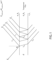
- FIG. 1 an illustration depicting transparent film errors caused by dielectric light propagation is shown, in accordance with one or more embodiments of the present disclosure.
- the resultant overall reflection is a superimposition of multiple reflections bounced back and forth between interfaces of all underlying layers.
- the phase change ⁇ due to reflection is dependent upon the layer structure of the wafer. More specifically, the phase change in the reflected beam is a function of film thickness, complex refractive index, and properties of the substrate. If the film is uniform, the phase change ⁇ is constant and does not introduce topography measurement error. If the film is non-uniform, as shown on FIG. 2 , the phase change ⁇ will deform topography, resulting in measurement errors.
- the reflectivity from such film stack can also be modeled as a function of the film n, k, and thickness.
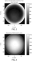
- FIGS. 3 and 4 are illustrations depicting a type of measurement error that may be referred to as inversion error, in accordance with one or more embodiments of the present disclosure.
- FIG. 4 shows a true film thickness of a wafer, which has a film of the center region thicker than the film of the edge region.
- various types of measurement tools may be utilized to assist in measuring the true film thickness.
- broadband ellipsometry film tools, on-tool broadband reflectometer thickness probes, capacitance gauges, optical thickness gauges, or the like may be utilized without departing from the scope of the present disclosure as defined by the appended claims.
- FIG. 1 broadband ellipsometry film tools, on-tool broadband reflectometer thickness probes, capacitance gauges, optical thickness gauges, or the like may be utilized without departing from the scope of the present disclosure as defined by the appended claims.
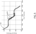
- the wafer thickness measured using interferometry data (e.g., measured using a PWG measurement tool) without transparent film error correction. It is noted that the wafer thickness measured using optical interferometry data is the opposite of the true thickness due to inversion error of the transparent film. This relationship is illustrated in FIG. 5 .
- the correction model includes a correction curve, as illustrated in FIG. 5 .
- the correction curve 504 is generated from simulation.
- the x-axis indicates true thickness, measured in nanometers (nm), which is determined via a point-to-point thickness measurement reference.
- the y-axis displays the measured, or apparent, thickness, which includes the error induced by the transparent film and is measured via an optical interferometer.
- Experimental data 502, representing both true thickness and PWG measured thickness may be collected to verify the correction curve 504. Once the correction curve 504 is obtained, subsequent PWG measured thickness is corrected using the correction curve 504 to produce thickness measurements that closely resemble the true thickness.
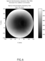
- FIG. 6 is a depiction of PWG measurement obtained before correction.
- the PWG measurement may then be corrected by applying a correction curve to it.
- the resulting measurement may be referred to as the corrected PWG measurement, which is shown in FIG. 7 .
- the corrected PWG measurement may accurately reflect the true thickness data, which is represented in FIG. 8 .
- the correlation between a corrected PWG thickness measurement and a reference tool (e.g., ellipsometer) thickness measurement may approach 97%.
- FIGS. 9A and 9B illustrate reflectivity information obtained from a film stack.
- FIG. 9A illustrates reflectivity measured across a sample using a PWG system.
- 9B illustrates the similarity between the measured reflectivity and the modeled reflectivity with respect to the film thickness change. It is noted that because only interferometry information post-film deposition is used for reflectivity measurement, this process may be accomplished in a single process step, which is more efficient than using two steps to measure surface topography before/after film deposition/etching to derive film thickness.
- phase unwrapping techniques may be applied to the correction curve described above to extend its thickness coverage to match a specific need.
- the correction process described above may be carried out by, but not limited to, one or more of the following algorithms: a fitting of interferometer intensity data, reflectivity, phase error vs. model result, a set of denoising/filtering techniques, a prediction algorithm, a statistical optimization algorithm, and a neural network algorithm with input from interferometer.
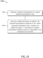
- FIG. 10 is a flow diagram depicting an embodiment of a correction process 1000 configured in accordance with the present disclosure.
- a wafer geometry system is utilized to obtain geometry measurements of a wafer in a step 1002.
- the geometry measurements obtained may include errors such as topography measurement errors and the like caused by transparent films positioned on the wafer.
- a correction model may then be utilized to help reduce the errors obtained in the geometry measurements in a step 1004.
- the correction model may help correct measurement errors caused by the transparent films positioned on the wafer.
- the correction model may be obtained a priori based on the correlation between true wafer thickness and measured wafer thickness data.
- the correction model may involve the use of a correction curve as previously described.
- the correction model may involve the use of both the a priori method and the correction curve method described above.
- the correction model may be dynamically updated in some embodiments. For instance, the output of step 1004 may be examined against some reference data to determine the effectiveness of the correction model. In some embodiments, a feedback loop may be provided to adjust the correction model if doing so can further reduce measurement errors. In some embodiments, the correction model may be generated based on the design of the wafer and known physical (and optical) properties of the various layers of the wafer. It is contemplated that various other types of techniques may be utilized to help generate/update the correction model without departing from the scope of the present disclosure as defined by the appended claims.
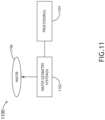
- the inspection system 1100 includes one or more wafer geometry tools 1102.
- the wafer geometry tool 1102 may be configured to obtain wafer geometry measurements from wafer 1106.
- the wafer geometry tool 1102 may include, but is not limited to, a dual cavity Fizeau interferometer.
- a description of a dual interferometer suitable for implementation in one or more embodiments of the present disclosure is provided in U.S. Patent No. 6,847,458, issued on January 25, 2005 .
- a description of a dual interferometer suitable for implementation in one or more embodiments of the present disclosure is provided in U.S. Patent No. 8,068,234, issued on November 29, 2011 .
- a description of a dual interferometer suitable for implementation in one or more embodiments of the present disclosure is provided in U.S. Patent Publication No. 2014/0293291, published on October 2, 2014 .
- the inspection system 1100 includes one or more processors 1104 (e.g., one or more computer processors).
- the one or more processors 1104 are communicatively coupled to the wafer geometry tool 1102 and configured to receive one or more measurements from the wafer geometry tool 1102.
- the one or more processors 1104 may be embodied in a controller.
- the processors 1104 may be configured to apply a correction model to the wafer geometry measurements obtained.
- the correction model may be obtained a priori.
- the correction model may also be dynamically adjustable as described above.
- the correction system and process described above enable accurate measurement of thick opaque film deposited on transparent film stacks, which is a key potential application in 3D NAND production.
- the correction system and process described above will significantly reduce transparent film induced topography measurement error without adding opaque film to fabrication process.
- the system 1100 is used to provide feedback and/or feedforward control in order to adjust upstream or downstream process tools in the 3D NAND fabrication facility.
- the one or more processors 1104 may include any one or more processing elements known in the art. It is to be understood that each of the processor(s) described herein may take various forms, including a personal computer system, image computer, mainframe computer system, workstation, network appliance, Internet appliance, or other device. In general, the term "computer system” may be broadly defined to encompass any device having one or more processors, which executes instructions from a memory medium.
- the computer subsystem(s) or system(s) may also include any suitable processor known in the art such as a parallel processor.
- the computer subsystem(s) or system(s) may include a computer platform with high speed processing and software, either as a standalone or a networked tool.
- a computer system includes more than one computer subsystems, then the different computer subsystems may be coupled to each other such that images, data, information, instructions, etc. can be sent between the computer subsystems as described further herein.
- one computer subsystem may be coupled to additional computer subsystem(s) by any suitable transmission media, which may include any suitable wired and/or wireless transmission media known in the art.
- Two or more of such computer subsystems may also be effectively coupled by a shared computer-readable storage medium.
- the term "processor” may be broadly defined to encompass any device having one or more processing elements, which execute program instructions from a non-transitory memory medium (i.e., memory).
- different subsystems of the system 1100 e.g., wafer geometry tool 1102, user interface, and the like
- the present disclosure relates also to a non-transitory computer-readable medium storing program instructions executable on a computer system for performing a computer-implemented method for target placement as described above.
- the computer-readable medium may be a storage medium such as a magnetic or optical disk, a magnetic tape, or any other suitable non-transitory computer-readable medium known in the art.
- the program instructions may be implemented in any of various ways, including procedure-based techniques, component-based techniques, and/or object-oriented techniques, among others.
- the program instructions may be implemented using ActiveX controls, C++ objects, JavaBeans, Microsoft Foundation Classes ("MFC"), SSE (Streaming SIMD Extension), or other technologies or methodologies, as desired.
- MFC Microsoft Foundation Classes
- SSE Streaming SIMD Extension
- wafer used in the present disclosure may include a thin slice of semiconductor material used in the fabrication of integrated circuits and other devices, as well as other thin polished plates such as magnetic disc substrates, gauge blocks, and the like.
- the methods and systems described in the present disclosure may be implemented as standalone products or as components of various wafer measurement, inspection, and/or hotspot discovery tools. It is understood that the specific order or hierarchy of steps in the methods disclosed are examples of exemplary approaches. Based upon design preferences, it is understood that the specific order or hierarchy of steps in the method can be rearranged while remaining within the scope and spirit of the disclosure. It is also understood that the various blocks depicted in the figures are presented separately for illustrative purposes. It is contemplated that while the various blocks depicted in the figures may be implemented as separate (and communicatively coupled) devices and/or processing units, they may also be integrated together without departing from the spirit and the scope of the present disclosure.
- All of the methods described herein may include storing results of one or more steps of the method embodiments in a memory medium.
- the results may include any of the results described herein and may be stored in any manner known in the art.
- the memory medium may include any memory medium described herein or any other suitable memory medium known in the art.
- the results can be accessed in the memory medium and used by any of the method or system embodiments described herein, formatted for display to a user, used by another software module, method, or system, etc.
- the results may be stored "permanently,” “semi-permanently,” temporarily,” or for some period of time.
- the memory medium may be random access memory (RAM), and the results may not necessarily persist indefinitely in the memory medium.
- each of the embodiments of the method described above may include any other step(s) of any other method(s) described herein.
- each of the embodiments of the method described above may be performed by any of the systems described herein.
- a typical data processing system generally includes one or more of a system unit housing, a video display device, a memory such as volatile and non-volatile memory, processors such as microprocessors and digital signal processors, computational entities such as operating systems, drivers, graphical user interfaces, applications programs, one or more interaction devices, such as a touch pad or screen, and/or control systems including feedback loops and control motors (e.g., feedback for sensing position and/or velocity, and control motors for moving and/or adjusting components and/or quantities).
- a typical data processing system may be implemented utilizing any suitable commercially available components, such as those typically found in data computing/communication and/or network computing/communication systems.
- any two components so associated can also be viewed as being “operably connected,” or “operably coupled,” to each other to achieve the desired functionality, and any two components capable of being so associated can also be viewed as being “operably couplable,” to each other to achieve the desired functionality.
- operably couplable include but are not limited to physically mateable and/or physically interacting components, and/or wirelessly interactable and/or wirelessly interacting components, and/or logically interacting and/or logically interactable components.
Landscapes
- Physics & Mathematics (AREA)
- General Physics & Mathematics (AREA)
- Engineering & Computer Science (AREA)
- Manufacturing & Machinery (AREA)
- Analytical Chemistry (AREA)
- Life Sciences & Earth Sciences (AREA)
- General Health & Medical Sciences (AREA)
- Chemical & Material Sciences (AREA)
- Immunology (AREA)
- Pathology (AREA)
- Health & Medical Sciences (AREA)
- Biochemistry (AREA)
- Computer Hardware Design (AREA)
- Microelectronics & Electronic Packaging (AREA)
- Power Engineering (AREA)
- Mathematical Physics (AREA)
- Length Measuring Devices By Optical Means (AREA)
- Seats For Vehicles (AREA)
Applications Claiming Priority (3)
| Application Number | Priority Date | Filing Date | Title |
|---|---|---|---|
| US201762443815P | 2017-01-09 | 2017-01-09 | |
| US15/649,259 US10571248B2 (en) | 2017-01-09 | 2017-07-13 | Transparent film error correction pattern in wafer geometry system |
| PCT/US2018/012673 WO2018129385A1 (en) | 2017-01-09 | 2018-01-05 | Transparent film error correction pattern in wafer geometry system |
Publications (3)
| Publication Number | Publication Date |
|---|---|
| EP3549159A1 EP3549159A1 (en) | 2019-10-09 |
| EP3549159A4 EP3549159A4 (en) | 2020-09-09 |
| EP3549159B1 true EP3549159B1 (en) | 2024-08-07 |
Family
ID=62782771
Family Applications (1)
| Application Number | Title | Priority Date | Filing Date |
|---|---|---|---|
| EP18735858.5A Active EP3549159B1 (en) | 2017-01-09 | 2018-01-05 | Transparent film error correction pattern in wafer geometry system |
Country Status (8)
| Country | Link |
|---|---|
| US (1) | US10571248B2 (enExample) |
| EP (1) | EP3549159B1 (enExample) |
| JP (1) | JP6917462B2 (enExample) |
| KR (1) | KR102301560B1 (enExample) |
| CN (1) | CN110419098B (enExample) |
| SG (1) | SG11201906177WA (enExample) |
| TW (1) | TWI752146B (enExample) |
| WO (1) | WO2018129385A1 (enExample) |
Families Citing this family (9)
| Publication number | Priority date | Publication date | Assignee | Title |
|---|---|---|---|---|
| US10317198B2 (en) * | 2016-09-30 | 2019-06-11 | Kla-Tencor Corporation | Three-dimensional mapping of a wafer |
| US11067902B2 (en) * | 2017-08-07 | 2021-07-20 | Asml Netherlands B.V. | Computational metrology |
| EP3489619B1 (en) | 2017-11-28 | 2025-08-13 | Koh Young Technology Inc. | Apparatus for inspecting substrate and method thereof |
| US10852125B2 (en) * | 2017-11-28 | 2020-12-01 | Koh Young Technology Inc. | Apparatus for inspecting film on substrate by using optical interference and method thereof |
| US11112234B2 (en) * | 2018-03-07 | 2021-09-07 | Applejack 199 L.P. | Multi-probe gauge for slab characterization |
| JP6402273B1 (ja) * | 2018-05-18 | 2018-10-10 | 大塚電子株式会社 | 光学測定装置及び光学測定方法 |
| US11049720B2 (en) * | 2018-10-19 | 2021-06-29 | Kla Corporation | Removable opaque coating for accurate optical topography measurements on top surfaces of transparent films |
| EP3918384A1 (en) * | 2019-01-31 | 2021-12-08 | King Abdullah University of Science and Technology | Light processing device based on multilayer nano-elements |
| US20250044073A1 (en) * | 2023-08-04 | 2025-02-06 | Orbotech Ltd. | Thin film thickness adjustments for three-dimensional interferometric measurements |
Family Cites Families (24)
| Publication number | Priority date | Publication date | Assignee | Title |
|---|---|---|---|---|
| US5042949A (en) | 1989-03-17 | 1991-08-27 | Greenberg Jeffrey S | Optical profiler for films and substrates |
| US5129724A (en) * | 1991-01-29 | 1992-07-14 | Wyko Corporation | Apparatus and method for simultaneous measurement of film thickness and surface height variation for film-substrate sample |
| US7324214B2 (en) * | 2003-03-06 | 2008-01-29 | Zygo Corporation | Interferometer and method for measuring characteristics of optically unresolved surface features |
| US6847458B2 (en) | 2003-03-20 | 2005-01-25 | Phase Shift Technology, Inc. | Method and apparatus for measuring the shape and thickness variation of polished opaque plates |
| JP4192038B2 (ja) * | 2003-06-04 | 2008-12-03 | 東レエンジニアリング株式会社 | 表面形状および/または膜厚測定方法及びその装置 |
| US7292346B2 (en) * | 2003-09-15 | 2007-11-06 | Zygo Corporation | Triangulation methods and systems for profiling surfaces through a thin film coating |
| CA2559324A1 (en) * | 2004-03-11 | 2005-09-22 | Nano-Or Technologies (Israel) Ltd. | Methods and apparatus for wavefront manipulations and improved 3-d measurements |
| US7595891B2 (en) * | 2005-07-09 | 2009-09-29 | Kla-Tencor Corporation | Measurement of the top surface of an object with/without transparent thin films in white light interferometry |
| GB0712605D0 (en) * | 2007-06-28 | 2007-08-08 | Microsharp Corp Ltd | Optical film |
| CL2008003281A1 (es) * | 2007-11-02 | 2009-10-16 | Agc Flat Glass Na Inc | Metodo para fabricar una pelicula delgada que comprende suministrar un substrato, depositar una primera capa sobre el, depositar una segunda capa que comprende oxido de sn y/o zn sobre una porcion de la primera capa, en presencia de un agente oxidante a alta temperatura aumentando la conductividad electrica de la segunda capa. |
| US8068234B2 (en) | 2009-02-18 | 2011-11-29 | Kla-Tencor Corporation | Method and apparatus for measuring shape or thickness information of a substrate |
| US8395191B2 (en) * | 2009-10-12 | 2013-03-12 | Monolithic 3D Inc. | Semiconductor device and structure |
| CN102483582B (zh) | 2009-08-24 | 2016-01-20 | Asml荷兰有限公司 | 量测方法和设备、光刻设备、光刻处理单元和包括量测目标的衬底 |
| MY186210A (en) | 2010-07-23 | 2021-06-30 | First Solar Inc | In-line metrology system and method |
| US20120089365A1 (en) * | 2010-10-08 | 2012-04-12 | Zygo Corporation | Data interpolation methods for metrology of surfaces, films and underresolved structures |
| US8818754B2 (en) * | 2011-04-22 | 2014-08-26 | Nanometrics Incorporated | Thin films and surface topography measurement using reduced library |
| US8552369B2 (en) * | 2011-05-03 | 2013-10-08 | International Business Machines Corporation | Obtaining elemental concentration profile of sample |
| US9385058B1 (en) * | 2012-12-29 | 2016-07-05 | Monolithic 3D Inc. | Semiconductor device and structure |
| US20140293291A1 (en) | 2013-04-01 | 2014-10-02 | Kla-Tencor Corporation | Wafer Shape and Thickness Measurement System Utilizing Shearing Interferometers |
| US9189705B2 (en) * | 2013-08-08 | 2015-11-17 | JSMSW Technology LLC | Phase-controlled model-based overlay measurement systems and methods |
| JP5871242B2 (ja) * | 2013-10-30 | 2016-03-01 | レーザーテック株式会社 | 膜厚測定装置及び膜厚測定方法 |
| JP6635110B2 (ja) * | 2015-03-24 | 2020-01-22 | コニカミノルタ株式会社 | ポリイミド系光学フィルム、その製造方法及び有機エレクトロルミネッセンスディスプレイ |
| JP6321579B2 (ja) | 2015-06-01 | 2018-05-09 | 株式会社日立国際電気 | 半導体装置の製造方法、基板処理システム、基板処理装置及びプログラム |
| EP3150959B1 (en) * | 2015-10-02 | 2018-12-26 | Soitec | Method for measuring thickness variations in a layer of a multilayer semiconductor structure |
-
2017
- 2017-07-13 US US15/649,259 patent/US10571248B2/en active Active
-
2018
- 2018-01-05 JP JP2019537105A patent/JP6917462B2/ja active Active
- 2018-01-05 KR KR1020197022676A patent/KR102301560B1/ko active Active
- 2018-01-05 EP EP18735858.5A patent/EP3549159B1/en active Active
- 2018-01-05 SG SG11201906177WA patent/SG11201906177WA/en unknown
- 2018-01-05 CN CN201880011565.6A patent/CN110419098B/zh active Active
- 2018-01-05 WO PCT/US2018/012673 patent/WO2018129385A1/en not_active Ceased
- 2018-01-08 TW TW107100588A patent/TWI752146B/zh active
Also Published As
| Publication number | Publication date |
|---|---|
| WO2018129385A1 (en) | 2018-07-12 |
| US20180195855A1 (en) | 2018-07-12 |
| KR20190097281A (ko) | 2019-08-20 |
| TW201839876A (zh) | 2018-11-01 |
| CN110419098B (zh) | 2021-02-02 |
| CN110419098A (zh) | 2019-11-05 |
| TWI752146B (zh) | 2022-01-11 |
| EP3549159A1 (en) | 2019-10-09 |
| JP2020503526A (ja) | 2020-01-30 |
| US10571248B2 (en) | 2020-02-25 |
| JP6917462B2 (ja) | 2021-08-11 |
| EP3549159A4 (en) | 2020-09-09 |
| KR102301560B1 (ko) | 2021-09-10 |
| SG11201906177WA (en) | 2019-08-27 |
Similar Documents
| Publication | Publication Date | Title |
|---|---|---|
| EP3549159B1 (en) | Transparent film error correction pattern in wafer geometry system | |
| TWI609283B (zh) | 對參數追蹤最佳化之計量系統及使用於計量系統之方法 | |
| KR102220435B1 (ko) | 웨이퍼에 걸친 파라미터 변동들에 기초한 측정 모델 최적화 | |
| JP6762317B2 (ja) | 基板の面内歪みを検査する方法およびシステム | |
| CN110312911B (zh) | 用于测量衬底及膜厚度分布的系统及方法 | |
| EP2979297A1 (en) | Statistical model-based metrology | |
| US7930113B1 (en) | Measuring stresses in multi-layer thin film systems with variable film thickness | |
| CN118315306A (zh) | 半导体生产期间的过程诱导位移表征 | |
| US10955359B2 (en) | Method for quantification of process non uniformity using model-based metrology | |
| JP4131670B2 (ja) | 3次元の屈折率分布の干渉決定 | |
| TWI603070B (zh) | 使用於複雜之圖案化結構的量測之方法及系統 | |
| Wang et al. | A novel high-precision measurement method for warpage and bow of double-sided polished wafers based on wavelength-tunable laser interferometry | |
| CN118254096B (zh) | 用于原位测量膜厚的方法、参考光谱生成方法及设备 | |
| WO2025246244A1 (zh) | 用于原位测量膜厚的方法、参考光谱生成方法及设备 | |
| WO2025246242A1 (zh) | 晶圆磨削场景中近表面层介质的参数确定方法及设备 | |
| Huang et al. | Improvement of least squares integration method with iterative compensation for shape reconstruction from gradient | |
| CN118254098A (zh) | 用于原位测量膜厚的方法、参考光谱生成方法及设备 |
Legal Events
| Date | Code | Title | Description |
|---|---|---|---|
| STAA | Information on the status of an ep patent application or granted ep patent |
Free format text: STATUS: THE INTERNATIONAL PUBLICATION HAS BEEN MADE |
|
| PUAI | Public reference made under article 153(3) epc to a published international application that has entered the european phase |
Free format text: ORIGINAL CODE: 0009012 |
|
| STAA | Information on the status of an ep patent application or granted ep patent |
Free format text: STATUS: REQUEST FOR EXAMINATION WAS MADE |
|
| 17P | Request for examination filed |
Effective date: 20190704 |
|
| AK | Designated contracting states |
Kind code of ref document: A1 Designated state(s): AL AT BE BG CH CY CZ DE DK EE ES FI FR GB GR HR HU IE IS IT LI LT LU LV MC MK MT NL NO PL PT RO RS SE SI SK SM TR |
|
| AX | Request for extension of the european patent |
Extension state: BA ME |
|
| DAV | Request for validation of the european patent (deleted) | ||
| DAX | Request for extension of the european patent (deleted) | ||
| A4 | Supplementary search report drawn up and despatched |
Effective date: 20200810 |
|
| RIC1 | Information provided on ipc code assigned before grant |
Ipc: G01B 11/06 20060101ALI20200804BHEP Ipc: G01B 21/04 20060101ALI20200804BHEP Ipc: H01L 21/66 20060101AFI20200804BHEP Ipc: G01N 21/95 20060101ALI20200804BHEP Ipc: G01B 11/24 20060101ALI20200804BHEP Ipc: G01N 21/84 20060101ALI20200804BHEP |
|
| STAA | Information on the status of an ep patent application or granted ep patent |
Free format text: STATUS: EXAMINATION IS IN PROGRESS |
|
| 17Q | First examination report despatched |
Effective date: 20221111 |
|
| P01 | Opt-out of the competence of the unified patent court (upc) registered |
Effective date: 20230526 |
|
| GRAP | Despatch of communication of intention to grant a patent |
Free format text: ORIGINAL CODE: EPIDOSNIGR1 |
|
| STAA | Information on the status of an ep patent application or granted ep patent |
Free format text: STATUS: GRANT OF PATENT IS INTENDED |
|
| INTG | Intention to grant announced |
Effective date: 20240228 |
|
| GRAS | Grant fee paid |
Free format text: ORIGINAL CODE: EPIDOSNIGR3 |
|
| GRAA | (expected) grant |
Free format text: ORIGINAL CODE: 0009210 |
|
| STAA | Information on the status of an ep patent application or granted ep patent |
Free format text: STATUS: THE PATENT HAS BEEN GRANTED |
|
| AK | Designated contracting states |
Kind code of ref document: B1 Designated state(s): AL AT BE BG CH CY CZ DE DK EE ES FI FR GB GR HR HU IE IS IT LI LT LU LV MC MK MT NL NO PL PT RO RS SE SI SK SM TR |
|
| REG | Reference to a national code |
Ref country code: GB Ref legal event code: FG4D |
|
| REG | Reference to a national code |
Ref country code: CH Ref legal event code: EP |
|
| REG | Reference to a national code |
Ref country code: NL Ref legal event code: FP Ref country code: IE Ref legal event code: FG4D |
|
| REG | Reference to a national code |
Ref country code: DE Ref legal event code: R096 Ref document number: 602018072745 Country of ref document: DE |
|
| REG | Reference to a national code |
Ref country code: LT Ref legal event code: MG9D |
|
| PG25 | Lapsed in a contracting state [announced via postgrant information from national office to epo] |
Ref country code: NO Free format text: LAPSE BECAUSE OF FAILURE TO SUBMIT A TRANSLATION OF THE DESCRIPTION OR TO PAY THE FEE WITHIN THE PRESCRIBED TIME-LIMIT Effective date: 20241107 |
|
| REG | Reference to a national code |
Ref country code: AT Ref legal event code: MK05 Ref document number: 1711926 Country of ref document: AT Kind code of ref document: T Effective date: 20240807 |
|
| PG25 | Lapsed in a contracting state [announced via postgrant information from national office to epo] |
Ref country code: PT Free format text: LAPSE BECAUSE OF FAILURE TO SUBMIT A TRANSLATION OF THE DESCRIPTION OR TO PAY THE FEE WITHIN THE PRESCRIBED TIME-LIMIT Effective date: 20241209 Ref country code: FI Free format text: LAPSE BECAUSE OF FAILURE TO SUBMIT A TRANSLATION OF THE DESCRIPTION OR TO PAY THE FEE WITHIN THE PRESCRIBED TIME-LIMIT Effective date: 20240807 Ref country code: PL Free format text: LAPSE BECAUSE OF FAILURE TO SUBMIT A TRANSLATION OF THE DESCRIPTION OR TO PAY THE FEE WITHIN THE PRESCRIBED TIME-LIMIT Effective date: 20240807 Ref country code: GR Free format text: LAPSE BECAUSE OF FAILURE TO SUBMIT A TRANSLATION OF THE DESCRIPTION OR TO PAY THE FEE WITHIN THE PRESCRIBED TIME-LIMIT Effective date: 20241108 |
|
| PG25 | Lapsed in a contracting state [announced via postgrant information from national office to epo] |
Ref country code: BG Free format text: LAPSE BECAUSE OF FAILURE TO SUBMIT A TRANSLATION OF THE DESCRIPTION OR TO PAY THE FEE WITHIN THE PRESCRIBED TIME-LIMIT Effective date: 20240807 |
|
| PG25 | Lapsed in a contracting state [announced via postgrant information from national office to epo] |
Ref country code: LV Free format text: LAPSE BECAUSE OF FAILURE TO SUBMIT A TRANSLATION OF THE DESCRIPTION OR TO PAY THE FEE WITHIN THE PRESCRIBED TIME-LIMIT Effective date: 20240807 |
|
| PG25 | Lapsed in a contracting state [announced via postgrant information from national office to epo] |
Ref country code: AT Free format text: LAPSE BECAUSE OF FAILURE TO SUBMIT A TRANSLATION OF THE DESCRIPTION OR TO PAY THE FEE WITHIN THE PRESCRIBED TIME-LIMIT Effective date: 20240807 Ref country code: IS Free format text: LAPSE BECAUSE OF FAILURE TO SUBMIT A TRANSLATION OF THE DESCRIPTION OR TO PAY THE FEE WITHIN THE PRESCRIBED TIME-LIMIT Effective date: 20241207 |
|
| PG25 | Lapsed in a contracting state [announced via postgrant information from national office to epo] |
Ref country code: HR Free format text: LAPSE BECAUSE OF FAILURE TO SUBMIT A TRANSLATION OF THE DESCRIPTION OR TO PAY THE FEE WITHIN THE PRESCRIBED TIME-LIMIT Effective date: 20240807 |
|
| PG25 | Lapsed in a contracting state [announced via postgrant information from national office to epo] |
Ref country code: ES Free format text: LAPSE BECAUSE OF FAILURE TO SUBMIT A TRANSLATION OF THE DESCRIPTION OR TO PAY THE FEE WITHIN THE PRESCRIBED TIME-LIMIT Effective date: 20240807 Ref country code: RS Free format text: LAPSE BECAUSE OF FAILURE TO SUBMIT A TRANSLATION OF THE DESCRIPTION OR TO PAY THE FEE WITHIN THE PRESCRIBED TIME-LIMIT Effective date: 20241107 |
|
| PG25 | Lapsed in a contracting state [announced via postgrant information from national office to epo] |
Ref country code: RS Free format text: LAPSE BECAUSE OF FAILURE TO SUBMIT A TRANSLATION OF THE DESCRIPTION OR TO PAY THE FEE WITHIN THE PRESCRIBED TIME-LIMIT Effective date: 20241107 Ref country code: PT Free format text: LAPSE BECAUSE OF FAILURE TO SUBMIT A TRANSLATION OF THE DESCRIPTION OR TO PAY THE FEE WITHIN THE PRESCRIBED TIME-LIMIT Effective date: 20241209 Ref country code: PL Free format text: LAPSE BECAUSE OF FAILURE TO SUBMIT A TRANSLATION OF THE DESCRIPTION OR TO PAY THE FEE WITHIN THE PRESCRIBED TIME-LIMIT Effective date: 20240807 Ref country code: NO Free format text: LAPSE BECAUSE OF FAILURE TO SUBMIT A TRANSLATION OF THE DESCRIPTION OR TO PAY THE FEE WITHIN THE PRESCRIBED TIME-LIMIT Effective date: 20241107 Ref country code: LV Free format text: LAPSE BECAUSE OF FAILURE TO SUBMIT A TRANSLATION OF THE DESCRIPTION OR TO PAY THE FEE WITHIN THE PRESCRIBED TIME-LIMIT Effective date: 20240807 Ref country code: IS Free format text: LAPSE BECAUSE OF FAILURE TO SUBMIT A TRANSLATION OF THE DESCRIPTION OR TO PAY THE FEE WITHIN THE PRESCRIBED TIME-LIMIT Effective date: 20241207 Ref country code: HR Free format text: LAPSE BECAUSE OF FAILURE TO SUBMIT A TRANSLATION OF THE DESCRIPTION OR TO PAY THE FEE WITHIN THE PRESCRIBED TIME-LIMIT Effective date: 20240807 Ref country code: GR Free format text: LAPSE BECAUSE OF FAILURE TO SUBMIT A TRANSLATION OF THE DESCRIPTION OR TO PAY THE FEE WITHIN THE PRESCRIBED TIME-LIMIT Effective date: 20241108 Ref country code: FI Free format text: LAPSE BECAUSE OF FAILURE TO SUBMIT A TRANSLATION OF THE DESCRIPTION OR TO PAY THE FEE WITHIN THE PRESCRIBED TIME-LIMIT Effective date: 20240807 Ref country code: ES Free format text: LAPSE BECAUSE OF FAILURE TO SUBMIT A TRANSLATION OF THE DESCRIPTION OR TO PAY THE FEE WITHIN THE PRESCRIBED TIME-LIMIT Effective date: 20240807 Ref country code: BG Free format text: LAPSE BECAUSE OF FAILURE TO SUBMIT A TRANSLATION OF THE DESCRIPTION OR TO PAY THE FEE WITHIN THE PRESCRIBED TIME-LIMIT Effective date: 20240807 Ref country code: AT Free format text: LAPSE BECAUSE OF FAILURE TO SUBMIT A TRANSLATION OF THE DESCRIPTION OR TO PAY THE FEE WITHIN THE PRESCRIBED TIME-LIMIT Effective date: 20240807 |
|
| PGFP | Annual fee paid to national office [announced via postgrant information from national office to epo] |
Ref country code: NL Payment date: 20250127 Year of fee payment: 8 |
|
| PGFP | Annual fee paid to national office [announced via postgrant information from national office to epo] |
Ref country code: DE Payment date: 20250129 Year of fee payment: 8 |
|
| PG25 | Lapsed in a contracting state [announced via postgrant information from national office to epo] |
Ref country code: SM Free format text: LAPSE BECAUSE OF FAILURE TO SUBMIT A TRANSLATION OF THE DESCRIPTION OR TO PAY THE FEE WITHIN THE PRESCRIBED TIME-LIMIT Effective date: 20240807 Ref country code: RO Free format text: LAPSE BECAUSE OF FAILURE TO SUBMIT A TRANSLATION OF THE DESCRIPTION OR TO PAY THE FEE WITHIN THE PRESCRIBED TIME-LIMIT Effective date: 20240807 Ref country code: DK Free format text: LAPSE BECAUSE OF FAILURE TO SUBMIT A TRANSLATION OF THE DESCRIPTION OR TO PAY THE FEE WITHIN THE PRESCRIBED TIME-LIMIT Effective date: 20240807 |
|
| PG25 | Lapsed in a contracting state [announced via postgrant information from national office to epo] |
Ref country code: EE Free format text: LAPSE BECAUSE OF FAILURE TO SUBMIT A TRANSLATION OF THE DESCRIPTION OR TO PAY THE FEE WITHIN THE PRESCRIBED TIME-LIMIT Effective date: 20240807 |
|
| PG25 | Lapsed in a contracting state [announced via postgrant information from national office to epo] |
Ref country code: CZ Free format text: LAPSE BECAUSE OF FAILURE TO SUBMIT A TRANSLATION OF THE DESCRIPTION OR TO PAY THE FEE WITHIN THE PRESCRIBED TIME-LIMIT Effective date: 20240807 |
|
| PG25 | Lapsed in a contracting state [announced via postgrant information from national office to epo] |
Ref country code: SK Free format text: LAPSE BECAUSE OF FAILURE TO SUBMIT A TRANSLATION OF THE DESCRIPTION OR TO PAY THE FEE WITHIN THE PRESCRIBED TIME-LIMIT Effective date: 20240807 |
|
| REG | Reference to a national code |
Ref country code: DE Ref legal event code: R097 Ref document number: 602018072745 Country of ref document: DE |
|
| PLBE | No opposition filed within time limit |
Free format text: ORIGINAL CODE: 0009261 |
|
| STAA | Information on the status of an ep patent application or granted ep patent |
Free format text: STATUS: NO OPPOSITION FILED WITHIN TIME LIMIT |
|
| 26N | No opposition filed |
Effective date: 20250508 |
|
| REG | Reference to a national code |
Ref country code: CH Ref legal event code: PL |
|
| PG25 | Lapsed in a contracting state [announced via postgrant information from national office to epo] |
Ref country code: SE Free format text: LAPSE BECAUSE OF FAILURE TO SUBMIT A TRANSLATION OF THE DESCRIPTION OR TO PAY THE FEE WITHIN THE PRESCRIBED TIME-LIMIT Effective date: 20240807 |
|
| PG25 | Lapsed in a contracting state [announced via postgrant information from national office to epo] |
Ref country code: LU Free format text: LAPSE BECAUSE OF NON-PAYMENT OF DUE FEES Effective date: 20250105 Ref country code: MC Free format text: LAPSE BECAUSE OF FAILURE TO SUBMIT A TRANSLATION OF THE DESCRIPTION OR TO PAY THE FEE WITHIN THE PRESCRIBED TIME-LIMIT Effective date: 20240807 |
|
| GBPC | Gb: european patent ceased through non-payment of renewal fee |
Effective date: 20250105 |
|
| PG25 | Lapsed in a contracting state [announced via postgrant information from national office to epo] |
Ref country code: GB Free format text: LAPSE BECAUSE OF NON-PAYMENT OF DUE FEES Effective date: 20250105 Ref country code: BE Free format text: LAPSE BECAUSE OF NON-PAYMENT OF DUE FEES Effective date: 20250131 |
|
| PG25 | Lapsed in a contracting state [announced via postgrant information from national office to epo] |
Ref country code: FR Free format text: LAPSE BECAUSE OF NON-PAYMENT OF DUE FEES Effective date: 20250131 |
|
| PG25 | Lapsed in a contracting state [announced via postgrant information from national office to epo] |
Ref country code: CH Free format text: LAPSE BECAUSE OF NON-PAYMENT OF DUE FEES Effective date: 20250131 |
|
| REG | Reference to a national code |
Ref country code: BE Ref legal event code: MM Effective date: 20250131 |