EP3544392B1 - Electronic device and method for producing same - Google Patents
Electronic device and method for producing same Download PDFInfo
- Publication number
- EP3544392B1 EP3544392B1 EP17871776.5A EP17871776A EP3544392B1 EP 3544392 B1 EP3544392 B1 EP 3544392B1 EP 17871776 A EP17871776 A EP 17871776A EP 3544392 B1 EP3544392 B1 EP 3544392B1
- Authority
- EP
- European Patent Office
- Prior art keywords
- molded body
- resin molded
- interconnection
- electronic device
- bend portion
- Prior art date
- Legal status (The legal status is an assumption and is not a legal conclusion. Google has not performed a legal analysis and makes no representation as to the accuracy of the status listed.)
- Active
Links
Images




Classifications
-
- H—ELECTRICITY
- H10—SEMICONDUCTOR DEVICES; ELECTRIC SOLID-STATE DEVICES NOT OTHERWISE PROVIDED FOR
- H10W—GENERIC PACKAGES, INTERCONNECTIONS, CONNECTORS OR OTHER CONSTRUCTIONAL DETAILS OF DEVICES COVERED BY CLASS H10
- H10W74/00—Encapsulations, e.g. protective coatings
- H10W74/01—Manufacture or treatment
- H10W74/016—Manufacture or treatment using moulds
-
- H—ELECTRICITY
- H10—SEMICONDUCTOR DEVICES; ELECTRIC SOLID-STATE DEVICES NOT OTHERWISE PROVIDED FOR
- H10W—GENERIC PACKAGES, INTERCONNECTIONS, CONNECTORS OR OTHER CONSTRUCTIONAL DETAILS OF DEVICES COVERED BY CLASS H10
- H10W74/00—Encapsulations, e.g. protective coatings
- H10W74/01—Manufacture or treatment
-
- H—ELECTRICITY
- H05—ELECTRIC TECHNIQUES NOT OTHERWISE PROVIDED FOR
- H05K—PRINTED CIRCUITS; CASINGS OR CONSTRUCTIONAL DETAILS OF ELECTRIC APPARATUS; MANUFACTURE OF ASSEMBLAGES OF ELECTRICAL COMPONENTS
- H05K1/00—Printed circuits
- H05K1/02—Details
- H05K1/0277—Bendability or stretchability details
- H05K1/028—Bending or folding regions of flexible printed circuits
-
- H—ELECTRICITY
- H05—ELECTRIC TECHNIQUES NOT OTHERWISE PROVIDED FOR
- H05K—PRINTED CIRCUITS; CASINGS OR CONSTRUCTIONAL DETAILS OF ELECTRIC APPARATUS; MANUFACTURE OF ASSEMBLAGES OF ELECTRICAL COMPONENTS
- H05K1/00—Printed circuits
- H05K1/02—Details
- H05K1/14—Structural association of two or more printed circuits
- H05K1/147—Structural association of two or more printed circuits at least one of the printed circuits being bent or folded, e.g. by using a flexible printed circuit
-
- H—ELECTRICITY
- H05—ELECTRIC TECHNIQUES NOT OTHERWISE PROVIDED FOR
- H05K—PRINTED CIRCUITS; CASINGS OR CONSTRUCTIONAL DETAILS OF ELECTRIC APPARATUS; MANUFACTURE OF ASSEMBLAGES OF ELECTRICAL COMPONENTS
- H05K3/00—Apparatus or processes for manufacturing printed circuits
- H05K3/22—Secondary treatment of printed circuits
- H05K3/28—Applying non-metallic protective coatings
- H05K3/284—Applying non-metallic protective coatings for encapsulating mounted components
-
- H—ELECTRICITY
- H10—SEMICONDUCTOR DEVICES; ELECTRIC SOLID-STATE DEVICES NOT OTHERWISE PROVIDED FOR
- H10W—GENERIC PACKAGES, INTERCONNECTIONS, CONNECTORS OR OTHER CONSTRUCTIONAL DETAILS OF DEVICES COVERED BY CLASS H10
- H10W70/00—Package substrates; Interposers; Redistribution layers [RDL]
- H10W70/60—Insulating or insulated package substrates; Interposers; Redistribution layers
- H10W70/611—Insulating or insulated package substrates; Interposers; Redistribution layers for connecting multiple chips together
-
- H—ELECTRICITY
- H10—SEMICONDUCTOR DEVICES; ELECTRIC SOLID-STATE DEVICES NOT OTHERWISE PROVIDED FOR
- H10W—GENERIC PACKAGES, INTERCONNECTIONS, CONNECTORS OR OTHER CONSTRUCTIONAL DETAILS OF DEVICES COVERED BY CLASS H10
- H10W70/00—Package substrates; Interposers; Redistribution layers [RDL]
- H10W70/60—Insulating or insulated package substrates; Interposers; Redistribution layers
- H10W70/67—Insulating or insulated package substrates; Interposers; Redistribution layers characterised by their insulating layers or insulating parts
- H10W70/688—Flexible insulating substrates
-
- H—ELECTRICITY
- H10—SEMICONDUCTOR DEVICES; ELECTRIC SOLID-STATE DEVICES NOT OTHERWISE PROVIDED FOR
- H10W—GENERIC PACKAGES, INTERCONNECTIONS, CONNECTORS OR OTHER CONSTRUCTIONAL DETAILS OF DEVICES COVERED BY CLASS H10
- H10W72/00—Interconnections or connectors in packages
- H10W72/01—Manufacture or treatment
- H10W72/019—Manufacture or treatment of bond pads
-
- H—ELECTRICITY
- H10—SEMICONDUCTOR DEVICES; ELECTRIC SOLID-STATE DEVICES NOT OTHERWISE PROVIDED FOR
- H10W—GENERIC PACKAGES, INTERCONNECTIONS, CONNECTORS OR OTHER CONSTRUCTIONAL DETAILS OF DEVICES COVERED BY CLASS H10
- H10W74/00—Encapsulations, e.g. protective coatings
- H10W74/01—Manufacture or treatment
- H10W74/016—Manufacture or treatment using moulds
- H10W74/017—Auxiliary layers for moulds, e.g. release layers or layers preventing residue
-
- H—ELECTRICITY
- H10—SEMICONDUCTOR DEVICES; ELECTRIC SOLID-STATE DEVICES NOT OTHERWISE PROVIDED FOR
- H10W—GENERIC PACKAGES, INTERCONNECTIONS, CONNECTORS OR OTHER CONSTRUCTIONAL DETAILS OF DEVICES COVERED BY CLASS H10
- H10W74/00—Encapsulations, e.g. protective coatings
- H10W74/01—Manufacture or treatment
- H10W74/019—Manufacture or treatment using temporary auxiliary substrates
-
- H—ELECTRICITY
- H10—SEMICONDUCTOR DEVICES; ELECTRIC SOLID-STATE DEVICES NOT OTHERWISE PROVIDED FOR
- H10W—GENERIC PACKAGES, INTERCONNECTIONS, CONNECTORS OR OTHER CONSTRUCTIONAL DETAILS OF DEVICES COVERED BY CLASS H10
- H10W74/00—Encapsulations, e.g. protective coatings
- H10W74/10—Encapsulations, e.g. protective coatings characterised by their shape or disposition
- H10W74/111—Encapsulations, e.g. protective coatings characterised by their shape or disposition the semiconductor body being completely enclosed
-
- H—ELECTRICITY
- H10—SEMICONDUCTOR DEVICES; ELECTRIC SOLID-STATE DEVICES NOT OTHERWISE PROVIDED FOR
- H10W—GENERIC PACKAGES, INTERCONNECTIONS, CONNECTORS OR OTHER CONSTRUCTIONAL DETAILS OF DEVICES COVERED BY CLASS H10
- H10W74/00—Encapsulations, e.g. protective coatings
- H10W74/10—Encapsulations, e.g. protective coatings characterised by their shape or disposition
- H10W74/111—Encapsulations, e.g. protective coatings characterised by their shape or disposition the semiconductor body being completely enclosed
- H10W74/121—Encapsulations, e.g. protective coatings characterised by their shape or disposition the semiconductor body being completely enclosed by multiple encapsulations, e.g. by a thin protective coating and a thick encapsulation
-
- H—ELECTRICITY
- H05—ELECTRIC TECHNIQUES NOT OTHERWISE PROVIDED FOR
- H05K—PRINTED CIRCUITS; CASINGS OR CONSTRUCTIONAL DETAILS OF ELECTRIC APPARATUS; MANUFACTURE OF ASSEMBLAGES OF ELECTRICAL COMPONENTS
- H05K1/00—Printed circuits
- H05K1/02—Details
- H05K1/14—Structural association of two or more printed circuits
- H05K1/148—Arrangements of two or more hingeably connected rigid printed circuit boards, i.e. connected by flexible means
-
- H—ELECTRICITY
- H05—ELECTRIC TECHNIQUES NOT OTHERWISE PROVIDED FOR
- H05K—PRINTED CIRCUITS; CASINGS OR CONSTRUCTIONAL DETAILS OF ELECTRIC APPARATUS; MANUFACTURE OF ASSEMBLAGES OF ELECTRICAL COMPONENTS
- H05K2203/00—Indexing scheme relating to apparatus or processes for manufacturing printed circuits covered by H05K3/00
- H05K2203/01—Tools for processing; Objects used during processing
- H05K2203/0191—Using tape or non-metallic foil in a process, e.g. during filling of a hole with conductive paste
-
- H—ELECTRICITY
- H05—ELECTRIC TECHNIQUES NOT OTHERWISE PROVIDED FOR
- H05K—PRINTED CIRCUITS; CASINGS OR CONSTRUCTIONAL DETAILS OF ELECTRIC APPARATUS; MANUFACTURE OF ASSEMBLAGES OF ELECTRICAL COMPONENTS
- H05K2203/00—Indexing scheme relating to apparatus or processes for manufacturing printed circuits covered by H05K3/00
- H05K2203/13—Moulding and encapsulation; Deposition techniques; Protective layers
- H05K2203/1305—Moulding and encapsulation
- H05K2203/1316—Moulded encapsulation of mounted components
-
- H—ELECTRICITY
- H05—ELECTRIC TECHNIQUES NOT OTHERWISE PROVIDED FOR
- H05K—PRINTED CIRCUITS; CASINGS OR CONSTRUCTIONAL DETAILS OF ELECTRIC APPARATUS; MANUFACTURE OF ASSEMBLAGES OF ELECTRICAL COMPONENTS
- H05K2203/00—Indexing scheme relating to apparatus or processes for manufacturing printed circuits covered by H05K3/00
- H05K2203/14—Related to the order of processing steps
- H05K2203/1461—Applying or finishing the circuit pattern after another process, e.g. after filling of vias with conductive paste, after making printed resistors
- H05K2203/1469—Circuit made after mounting or encapsulation of the components
-
- H—ELECTRICITY
- H10—SEMICONDUCTOR DEVICES; ELECTRIC SOLID-STATE DEVICES NOT OTHERWISE PROVIDED FOR
- H10W—GENERIC PACKAGES, INTERCONNECTIONS, CONNECTORS OR OTHER CONSTRUCTIONAL DETAILS OF DEVICES COVERED BY CLASS H10
- H10W70/00—Package substrates; Interposers; Redistribution layers [RDL]
- H10W70/01—Manufacture or treatment
- H10W70/05—Manufacture or treatment of insulating or insulated package substrates, or of interposers, or of redistribution layers
- H10W70/093—Connecting or disconnecting other interconnections thereto or therefrom, e.g. connecting bond wires or bumps
-
- H—ELECTRICITY
- H10—SEMICONDUCTOR DEVICES; ELECTRIC SOLID-STATE DEVICES NOT OTHERWISE PROVIDED FOR
- H10W—GENERIC PACKAGES, INTERCONNECTIONS, CONNECTORS OR OTHER CONSTRUCTIONAL DETAILS OF DEVICES COVERED BY CLASS H10
- H10W70/00—Package substrates; Interposers; Redistribution layers [RDL]
- H10W70/60—Insulating or insulated package substrates; Interposers; Redistribution layers
-
- H—ELECTRICITY
- H10—SEMICONDUCTOR DEVICES; ELECTRIC SOLID-STATE DEVICES NOT OTHERWISE PROVIDED FOR
- H10W—GENERIC PACKAGES, INTERCONNECTIONS, CONNECTORS OR OTHER CONSTRUCTIONAL DETAILS OF DEVICES COVERED BY CLASS H10
- H10W70/00—Package substrates; Interposers; Redistribution layers [RDL]
- H10W70/60—Insulating or insulated package substrates; Interposers; Redistribution layers
- H10W70/611—Insulating or insulated package substrates; Interposers; Redistribution layers for connecting multiple chips together
- H10W70/614—Insulating or insulated package substrates; Interposers; Redistribution layers for connecting multiple chips together the multiple chips being integrally enclosed
-
- H—ELECTRICITY
- H10—SEMICONDUCTOR DEVICES; ELECTRIC SOLID-STATE DEVICES NOT OTHERWISE PROVIDED FOR
- H10W—GENERIC PACKAGES, INTERCONNECTIONS, CONNECTORS OR OTHER CONSTRUCTIONAL DETAILS OF DEVICES COVERED BY CLASS H10
- H10W70/00—Package substrates; Interposers; Redistribution layers [RDL]
- H10W70/60—Insulating or insulated package substrates; Interposers; Redistribution layers
- H10W70/62—Insulating or insulated package substrates; Interposers; Redistribution layers characterised by their interconnections
- H10W70/65—Shapes or dispositions of interconnections
- H10W70/654—Top-view layouts
-
- H—ELECTRICITY
- H10—SEMICONDUCTOR DEVICES; ELECTRIC SOLID-STATE DEVICES NOT OTHERWISE PROVIDED FOR
- H10W—GENERIC PACKAGES, INTERCONNECTIONS, CONNECTORS OR OTHER CONSTRUCTIONAL DETAILS OF DEVICES COVERED BY CLASS H10
- H10W72/00—Interconnections or connectors in packages
- H10W72/01—Manufacture or treatment
- H10W72/0198—Manufacture or treatment batch processes
-
- H—ELECTRICITY
- H10—SEMICONDUCTOR DEVICES; ELECTRIC SOLID-STATE DEVICES NOT OTHERWISE PROVIDED FOR
- H10W—GENERIC PACKAGES, INTERCONNECTIONS, CONNECTORS OR OTHER CONSTRUCTIONAL DETAILS OF DEVICES COVERED BY CLASS H10
- H10W72/00—Interconnections or connectors in packages
- H10W72/90—Bond pads, in general
- H10W72/941—Dispositions of bond pads
- H10W72/9413—Dispositions of bond pads on encapsulations
-
- H—ELECTRICITY
- H10—SEMICONDUCTOR DEVICES; ELECTRIC SOLID-STATE DEVICES NOT OTHERWISE PROVIDED FOR
- H10W—GENERIC PACKAGES, INTERCONNECTIONS, CONNECTORS OR OTHER CONSTRUCTIONAL DETAILS OF DEVICES COVERED BY CLASS H10
- H10W74/00—Encapsulations, e.g. protective coatings
- H10W74/10—Encapsulations, e.g. protective coatings characterised by their shape or disposition
-
- H—ELECTRICITY
- H10—SEMICONDUCTOR DEVICES; ELECTRIC SOLID-STATE DEVICES NOT OTHERWISE PROVIDED FOR
- H10W—GENERIC PACKAGES, INTERCONNECTIONS, CONNECTORS OR OTHER CONSTRUCTIONAL DETAILS OF DEVICES COVERED BY CLASS H10
- H10W90/00—Package configurations
-
- H—ELECTRICITY
- H10—SEMICONDUCTOR DEVICES; ELECTRIC SOLID-STATE DEVICES NOT OTHERWISE PROVIDED FOR
- H10W—GENERIC PACKAGES, INTERCONNECTIONS, CONNECTORS OR OTHER CONSTRUCTIONAL DETAILS OF DEVICES COVERED BY CLASS H10
- H10W90/00—Package configurations
- H10W90/10—Configurations of laterally-adjacent chips
-
- H—ELECTRICITY
- H10—SEMICONDUCTOR DEVICES; ELECTRIC SOLID-STATE DEVICES NOT OTHERWISE PROVIDED FOR
- H10W—GENERIC PACKAGES, INTERCONNECTIONS, CONNECTORS OR OTHER CONSTRUCTIONAL DETAILS OF DEVICES COVERED BY CLASS H10
- H10W90/00—Package configurations
- H10W90/401—Package configurations characterised by multiple insulating or insulated package substrates, interposers or RDLs
-
- H—ELECTRICITY
- H10—SEMICONDUCTOR DEVICES; ELECTRIC SOLID-STATE DEVICES NOT OTHERWISE PROVIDED FOR
- H10W—GENERIC PACKAGES, INTERCONNECTIONS, CONNECTORS OR OTHER CONSTRUCTIONAL DETAILS OF DEVICES COVERED BY CLASS H10
- H10W90/00—Package configurations
- H10W90/701—Package configurations characterised by the relative positions of pads or connectors relative to package parts
- H10W90/721—Package configurations characterised by the relative positions of pads or connectors relative to package parts of bump connectors
- H10W90/724—Package configurations characterised by the relative positions of pads or connectors relative to package parts of bump connectors between a chip and a stacked insulating package substrate, interposer or RDL
Definitions
- the present technique relates to a partially bendable electronic device and a method for manufacturing the same.
- the device has only a limited area for fixing a rigid substrate on which electronic components are mounted. Accordingly, a technique is known in which a bendable flexible substrate is used to connect a plurality of rigid substrates that are not in the same plane.
- Fig. 11 shows an example electronic device that combines rigid substrates and a flexible substrate.
- the electronic device shown in Fig. 11 includes rigid substrates 70, 75 and a flexible substrate 80.
- Rigid substrate 70 has an electronic component 71 mounted thereon, the electronic component 71 being connected to interconnections 72a, 72b formed on rigid substrate 70.
- Rigid substrate 75 has electronic components 76a, 76b mounted thereon, the electronic components 76a, 76b being connected to interconnections 77a to 77c formed on rigid substrate 75.
- a conductive layer 81 which is formed on flexible substrate 80, is connected to interconnection 72b of substrate 70 via a conductive adhesive layer 90a and is also connected to interconnection 77a of substrate 75 via a conductive adhesive layer 90b.
- substrates 70, 75 are electrically connected to each other via bendable flexible substrate 80.
- each of rigid substrates 70, 75 requires a terminal area for connection to flexible substrate 80, resulting in enlarged substrate area. Further, the increase in man-hour for assembly increases the manufacturing cost.
- Japanese Patent Laying-Open No. 6-177490 discloses a printed wiring board produced by integrating a flexible wiring board and rigid wiring boards together by sandwiching the flexible wiring board between the rigid wiring boards from above and below with adhesive layers being interposed.
- the flexible wiring board and the rigid wiring boards can be connected via interlayer circuit interconnections, such as through holes. This eliminates the need for a terminal area for connection to the flexible substrate, thus preventing enlarged substrate area.
- US 2016/327977 A1 discloses an integrated circuit (IC) package which may include a flexible substrate.
- the flexible substrate may have a plurality of dies coupled therewith.
- the IC package may include a first encapsulation material, having a first rigidity, disposed on the flexible substrate to at least partially encapsulate each die of the plurality dies.
- the IC package may further include a second encapsulation material, having a second rigidity, disposed on the flexible substrate.
- US 2008/257589 A1 discloses a method for the production of an expandable circuit carrier in which a starting material for an expandable substrate is applied on an electrically conductive foil which forms an expandable substrate layer which is connected to the foil, after which the foil is structured such that it forms a conductor structure having at least one expandable strip conductor.
- JP 2016 111037 A discloses a solar battery back protection sheet having a base material layer (PI layer) and an easy adhesive layer (P2 layer).
- the P1 layer is mainly composed of polyester resin and has the P2 layer at least on one side thereof.
- the printed wiring substrate is disadvantageously thick. Further, the printed wiring substrate is thicker by electronic components mounted on the printed wiring substrate via, for example, solder.
- the technique requires, for example, laminating press and a large apparatus for multi-layering the rigid wiring boards and the flexible substrate. This disadvantageously increases the manufacturing cost.
- An object of the present invention is to provide an electronic device including a bendable bend portion and having a reduced size and thickness, and also provide a method for manufacturing such an electronic device with reduced manufacturing cost.
- the material of the bend portion may be higher in breaking elongation percentage than the material of the resin molded body.
- the bend portion may be made of a resin having a breaking elongation percentage of 300% or more.
- the resin molded body may be made of a resin having a breaking elongation percentage of 150% or less.
- the resin molded body may contain a filler.
- a method for manufacturing an electronic device in accordance with the present invention is defined in claim 8.
- a second interconnection may be formed beforehand on a surface of the bend portion.
- the sticking may include sticking the bend portion to the sheet so that the second interconnection faces the sheet; and the forming the first interconnection may include forming the first interconnection so that the first interconnection is connected to the second interconnection.
- the present disclosure can provide an electronic device including a bendable bend portion and having a reduced size and thickness.
- Embodiments are described in detail with reference to the drawings. Only embodiments 4 and 5 are embodiments of the present invention. Embodiments 1 to 3 are illustrative embodiments that are useful for understanding the present invention. In the drawings, identical or corresponding parts are identically denoted, and the explanation thereof is not repeated.
- FIG. 1 is a plan view showing a schematic configuration of electronic device 100 in embodiment 1.
- Fig. 2 is a cross-sectional view taken along line X-X and seen in the arrow direction in Fig. 1 .
- Electronic device 100 is built in various types of electronic equipment, such as portable electronic equipment (e.g. wearable portable equipment), and a small-sized sensor, so that electronic device 100 performs a principal or auxiliary function of the electronic equipment.
- portable electronic equipment e.g. wearable portable equipment
- a small-sized sensor so that electronic device 100 performs a principal or auxiliary function of the electronic equipment.
- wearable portable equipment include a measuring instrument attached to clothes to measure a human body surface temperature; and a measuring instrument wound around an arm to measure a pulse, a blood pressure, or the like.
- electronic device 100 includes a main portion 10 having an electronic circuit formed thereon, a bendable bend portion 20, and an interconnection 30 (30a to 30h).
- Main portion 10 includes a resin molded body 11 and an electronic component 12 (12a to 12e).
- Resin molded body 11 is generally in the form of a plate and is made of resin, such as polycarbonate (PC) or acrylonitrile-butadiene-styrene (ABS).
- the shape of resin molded body 11 is not particularly limited, and may be designed as appropriate in accordance with the shape of electronic device 100.
- the material of resin molded body 11 may be other types of resin (e.g. polypropylene (PP), or elastomer).
- Resin molded body 11 has electronic component 12 (12a to 12e) embedded therein, thereby fixing electronic component 12. Resin molded body 11 has electronic component 12 embedded therein, so that electronic component 12 is exposed at an upper surface 11a.
- Electronic component 12 (12a to 12e) is, for example, a chip capacitor, a chip resistance, or an integrated circuit (IC).
- the number and type of electronic components 12 are not particularly limited.
- the surfaces of electronic components 12a to 12e exposed at resin molded body 11 respectively have electrodes 13a to 13e formed thereon.
- Bend portion 20 is continuous with resin molded body 11 and is bendable. Specifically, bend portion 20 is made of the same material as resin molded body 11 and is molded integrally with resin molded body 11. Bend portion 20 has a thickness t1 (e.g. 0.2 mm) thinner than a thickness t2 (e.g. 3 mm) of resin molded body 11 so that bend portion 20 is more bendable than resin molded body 11.
- t1 e.g. 0.2 mm
- t2 e.g. 3 mm
- the surface of bend portion 20 includes a continuous surface 20a continuous with upper surface 11a of resin molded body 11.
- two surfaces being “continuous” refers to a state in which the step between the two surfaces is so small that an interconnection formed on the surfaces does not break.
- continuous surface 20a of bend portion 20 is flush with upper surface 11a of resin molded body 11.
- Interconnection 30 (30a to 30h) is formed on at least upper surface 11a of upper surface 11a of resin molded body 11 and continuous surface 20a of bend portion 20. Interconnection 30 (30a to 30h) is connected to any of electrodes 13a to 13e of electronic components 12a to 12e.
- interconnections 30a to 30c are formed both on upper surface 11a of resin molded body 11 and on continuous surface 20a of bend portion 20, and continuously extend from electrode 13e of electronic component 12e, electrode 13d of electronic component 12d, and electrode 13b of electronic component 12b, respectively, to continuous surface 20a.
- Interconnections 30d to 30h are formed on upper surface 11a of resin molded body 11.
- Interconnection 30d is connected to electrode 13a of electronic component 12a and electrode 13b of electronic component 12b.
- Interconnection 30e is connected to electrode 13a of electronic component 12a and electrode 13c of electronic component 12c.
- Interconnection 30f is connected to electrode 13c of electronic component 12c and electrode 13d of electronic component 12d.
- Interconnection 30g is connected to electrode 13a of electronic component 12a and electrode 13d of electronic component 12d.
- Interconnection 30h is connected to electrode 13d of electronic component 12d and electrode 13e of electronic component 12e.
- Interconnection 30 can be easily formed by, for example, ink-jet printing with silver (Ag) ink.
- the ink-jet printing is a printing method in which ink is jetted from nozzles so that particulate ink deposits on a jetting target plane.
- interconnection 30 can be easily formed by ink-jet printing with silver (Ag) ink.
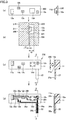
- FIG. 3 is a diagram explaining a method for manufacturing electronic device 100. Diagrams for explaining the first to fourth steps for manufacturing electronic device 100 are shown in (a) to (d) of Fig. 3 respectively.
- a plan view is shown on the left, and a side view is shown on the right.
- a cross-sectional view is shown.
- a plan view is shown on the left, and a cross-sectional view taken along line X-X and seen in the arrow direction in the plan view is shown on the right.
- Temporary fixation sheet 200 examples include polyethylene terephthalate (PET), polyethylene naphthalate (PEN), and polyphenylene sulfide (PPS).
- PET polyethylene terephthalate
- PEN polyethylene naphthalate
- PPS polyphenylene sulfide
- Temporary fixation sheet 200 is preferably made of a material transparent to ultraviolet rays and having flexibility for the reasons described later.
- the temporary fixation can be performed with, for example, an ultraviolet curable adhesive (not shown) applied to one side of temporary fixation sheet 200.
- an ultraviolet curable adhesive is applied, with a thickness of 2 to 3 ⁇ m, to PET temporary fixation sheet 200 having a thickness of 50 ⁇ m.
- This application may be performed by, for example, ink-jet printing.
- electronic components 12a to 12e are placed at prescribed positions.
- electronic components 12a to 12e are irradiated with ultraviolet rays having an intensity of, for example, 3000 mJ/cm 2 , from the side of temporary fixation sheet 200 on which electronic components 12a to 12e are not temporarily fixed.
- the adhesive cures and temporarily fixes electronic components 12a to 12e to temporary fixation sheet 200.
- temporary fixation sheet 200 having electronic components 12a to 12e temporarily fixed thereto is placed in a molding die formed by combining a first die 210 and a second die 220.
- first die 210 that faces second die 220 has a recess 211 having the same shape as temporary fixation sheet 200. In this recess 211, temporary fixation sheet 200 is fitted. Thus, the surface of temporary fixation sheet 200 having electronic components 12a to 12e stuck thereto faces second die 220.
- the depth of recess 211 is the same as the thickness of temporary fixation sheet 200. Accordingly, the surface of temporary fixation sheet 200 having electronic component 12 temporarily fixed thereto is flush with the surface of a part (where recess 211 is not formed) of first die 210 that faces second die 220.
- the surface of second die 220 that faces first die 210 has a shape such that a space 221 having a depth t2 is defined at the part that faces recess 211 of first die 210, and such that a space 222 having a depth t1 is defined at the part that does not face recess 211 of first die 210.
- Space 221 communicates with space 222.
- Injection molding of resin is performed by injecting resin material in spaces 221, 222 in the molding die formed by combining first die 210 and second die 220.
- the conditions for the injection molding may be selected as appropriate in accordance with the resin. If polycarbonate (PC) is used, the injection molding is performed under an injection resin temperature of 270°C and an injection pressure of 100 MPa, for example.
- PC polycarbonate
- resin material various types can be used.
- the conditions for the injection molding are not particularly limited.
- Structure 230 includes resin molded body 11 which has the same shape (thickness t2) as space 221 of the molding die, and a bend portion 20 which has the same shape (thickness t1) as space 222 of the molding die.
- temporary fixation sheet 200 is peeled from structure 230.
- surfaces of electronic components 12a to 12e are exposed at the sheet bonded surface (corresponding to upper surface 11a) of resin molded body 11 that has been in contact with temporary fixation sheet 200.
- temporary fixation sheet 200 is a PET film, it largely deforms due to thermal change during the second step. Thus, temporary fixation sheet 200 can be easily peeled from structure 230.
- interconnection 30 (30a to 30h) in a predetermined pattern is formed on upper surface 11a of resin molded body 11 and on continuous surface 20a of bend portion 20.
- interconnection 30 can be performed by a method of spraying conductive material (e.g. silver ink) by ink-jet printing, by a method using aerosol, or by a method using a dispenser, for example.
- conductive material e.g. silver ink
- interconnection 30 can be easily formed with a high degree of freedom of circuit design, and each of electronic components 12a to 12e can be electrically connected simply and easily with no solder. Further, in industrial terms, since electronic components 12a to 12e can be connected after their positions are determined, electronic components 12a to 12e can be electrically connected more correctly and easily than in the case in which the positions of electronic components are adjusted on a printed substrate, for example.
- electronic device 100 is completed, where electronic device 100 is provided with: main portion 10 including electronic component 12 and resin molded body 11; bend portion 20; and interconnection 30.
- electronic device 100 includes electronic component 12, resin molded body 11 in which electronic component 12 is embedded and fixed, and bendable bend portion 20 continuous with resin molded body 11.
- Resin molded body 11 in which electronic component 12 is embedded and fixed, serves as a substrate on which electronic components are mounted.
- electronic device 100 can be reduced in size and thickness compared to a conventional one in which electronic components are mounted on the upper surface of a rigid substrate via, for example, solder.
- bend portion 20 is continuous with resin molded body 11, electronic device 100 can be reduced in size and thickness compared to a case in which a flexible wiring board is sandwiched between rigid wiring boards from above and below (see Japanese Patent Laying-Open No. 6-177490 ).
- Bend portion 20 is molded integrally with resin molded body 11. Thus, there is no connecting point that receives mechanical load between bend portion 20 and resin molded body 11. This increases reliability in connection between resin molded body 11 and bend portion 20. Further, there is no need to use a separate flexible substrate, which is comparatively expensive. Thus the cost of components is reduced.
- the surface of resin molded body 11 includes upper surface (exposed surface) 11a at which electronic component 12 is exposed.
- the surface of bend portion 20 includes continuous surface 20a continuous with upper surface 11a.
- Electronic device 100 includes interconnection 30 formed on upper surface 11a and on continuous surface 20a, the interconnection 30 being connected to electronic component 12. This eliminates the need for a terminal area for electrically connecting the bend portion and resin molded body 11. Thus, further downsizing is achieved.
- Electronic device 100 is manufactured by the steps in the following (1) to (3):
- electrical connection between main portion 10 and bend portion 20 is achieved by forming interconnection 30 on upper surface 11a of resin molded body 11 and on continuous surface 20a of bend portion 20.
- An electronic device in embodiment 2 which is a variation of electronic device 100 in embodiment 1, is provided with a plurality of main portions each including an electronic component and a resin molded body.
- Fig. 4 is a plan view showing a schematic configuration of an electronic device 100A in embodiment 2.
- Fig. 5 is a cross-sectional view taken along line X-X and seen in the arrow direction in Fig. 4 .
- electronic device 100A is different from electronic device 100 in embodiment 1 in that electronic device 100A includes a main portion 40 and interconnections 30i to 30k.
- Main portion 40 is connected to an end of bend portion 20, opposite to the end connected to main portion 10.
- Main portion 40 includes a resin molded body 41 and an electronic component 42 (42a to 42c).
- Resin molded body 41 is generally in the form of a plate. Resin molded body 41 is made of the same resin as resin molded body 11 and bend portion 20. Also, resin molded body 41 is molded integrally with resin molded body 11 and bend portion 20.
- Resin molded body 41 has electronic component 42 (42a to 42c) embedded therein, thereby fixing electronic component 42.
- Resin molded body 41 has electronic component 42 embedded therein, so that electronic component 42 is exposed at an upper surface 41a.
- Upper surface 41a of resin molded body 41 is continuous with continuous surface 20a of bend portion 20 and is flush with upper surface 11a of resin molded body 11 and continuous surface 20a.
- Electronic component 42 (42a to 42c) is, for example, a chip capacitor, a chip resistance, or an integrated circuit (IC).
- the number and type of electronic components 42 are not particularly limited.
- the surfaces of electronic components 42a to 42c exposed at resin molded body 41 respectively have electrodes 43a to 43c formed thereon.
- Interconnections 30i to 30k are formed on upper surface 41a of resin molded body 41 and are connected to electrodes 43a to 43c of electronic components 42a to 42c.
- interconnections 30a to 30c formed on continuous surface 20a of bend portion 20 are extended to upper surface 41a of resin molded body 41.
- Interconnection 30a is connected to electrode 43b of electronic component 42b.
- Interconnections 30b, 30c are connected to electrode 43c of electronic component 42c.
- Electronic device 100A is manufactured in a method similar to that of embodiment 1. Specifically, in the first step described in embodiment 1, a temporary fixation sheet having electronic component 42 temporarily fixed thereto is prepared, separately from temporary fixation sheet 200 having electronic component 12 temporarily fixed thereto. In the second step, temporary fixation sheet 200 having electronic component 12 temporarily fixed thereto and the temporary fixation sheet having electronic component 42 temporarily fixed thereto are placed in a molding die. Then, the molding die is injected with resin material to perform injection molding of resin. Thus, resin molded bodies 11, 41 and bend portion 20 are integrally molded. After that, in the fourth step, interconnection 30 (30a to 30k) may be formed on upper surface 11a of resin molded body 11, on upper surface 41a of resin molded body 41, and on continuous surface 20a of bend portion 20 continuous with upper surfaces 11a, 41a.
- bendable bend portion 20 is disposed between a plurality of main portions 10, 40. Accordingly, even if main portion 10 and main portion 40 are placed not in the same plane, electronic device 100A can be built in electronic equipment, with the electronic circuit on main portion 10 being electrically connected to the electronic circuit on main portion 40 via bend portion 20.
- An electronic device in embodiment 3 is a variation of electronic device 100 in embodiment 1 or electronic device 100A in embodiment 2.
- the material of bend portion 20 is different from the material of resin molded body 11 of main portion 10 and resin molded body 41 of main portion 40.
- resin molded body 11 of main portion 10 and resin molded body 41 of main portion 40 are preferably made of a resin material having a breaking elongation percentage of 150% or less, such as polycarbonate (PC) or acrylonitrile-butadiene-styrene (ABS).
- the breaking elongation percentage refers to an elongation percentage of specimen at the time of breakage when a tensile test is performed in accordance with JIS K 7162, relative to the specimen before the test.
- main portions 10, 40 are less likely to deform and thus can be easily fixed in position.
- bend portion 20 is preferably made of a resin material having a breaking elongation percentage of 300% or more, such as polyurethane (PU), which has a breaking elongation percentage of 580%, or polyamide (PA), which has a breaking elongation percentage of 300%.
- PU polyurethane
- PA polyamide
- electronic device 100, 100A can be built in electronic equipment with bend portion 20 being elongated as necessary, depending on the other configuration of the electronic equipment in which electronic device 100, 100A is built, and depending on the positions at which main portions 10, 40 are placed.
- electronic device 100, 100A can be easily built in electronic equipment, even if there are variations in internal configuration among electronic equipments or even if some design change has been made in the internal configuration.
- bend portion 20 is placed near human joints.
- bend portion 20 made of a resin material having a breaking elongation percentage of 300% or more can expand and contract in accordance with the motion of the person wearing the clothes.
- Main portion 10 including a temperature sensor as electronic component 12 is placed at a comparatively stable position remote from human joints.
- Resin molded body 11 of main portion 10 preferably has elasticity to some degree in order to reduce stimulus to a human body when coming in contact with the human body surface.
- the resin material constituting resin molded body 11 is selected as appropriate from resin materials having a breaking elongation percentage of 150% or less, depending on the position at which main portion 10 is placed.
- bend portion 20 is made of the same resin material as resin molded body 11 of main portion 10 and resin molded body 41 of main portion 40, a filler (e.g. a glass filler or a carbon filler) is preferably added to the resin material constituting resin molded body 11 and resin molded body 41.
- a filler e.g. a glass filler or a carbon filler
- This can increase the intensity of main portions 10, 40.
- adding a glass filler is particularly preferable.
- a conventionally known method such as the two-color molding, may be used.
- the two-color molding is a method for integral molding by combining different resins or different materials. Specifically, resin molded body 11 is molded in a first molding die, and then bend portion 20 is molded in a second molding die, so that resin molded body 11 and bend portion 20 are integrally molded. Alternatively, bend portion 20 may be molded in a first molding die, and then resin molded body 11 may be molded in a second molding die, so that resin molded body 11 and bend portion 20 are integrally molded.
- bend portion 20 is made of a material having a high breaking elongation percentage, bend portion 20 may have the same thickness as resin molded body 11.
- bend portion 20 is molded by injection molding of resin material.
- an electronic device in embodiment 4 which is the first embodiment of the present invention, uses a flexible substrate as a bend portion.
- FIG. 6 is a plan view showing a schematic configuration of electronic device 100B in embodiment 4.
- Fig. 7 is a cross-sectional view taken along line X-X and seen in the arrow direction in Fig. 6 .
- electronic device 100B is different from electronic device 100 in embodiment 1 in that electronic device 100B includes a main portion 50 instead of main portion 10, and includes a bend portion 60 instead of bend portion 20.
- Bend portion 60 is a flexible substrate in the form of a film made of, for example, polyimide (PI) or polyethylene terephthalate (PET).
- the shape of bend portion 60 may be, but not limited to, a rectangular shape for example.
- the thickness of bend portion 60 may be, but not limited to, 50 ⁇ m for example.
- Main portion 50 is different from main portion 10 in embodiment 1 in that main portion 50 includes a resin molded body 51, instead of resin molded body 11.
- Resin molded body 51 is generally in the form of a plate and is made of resin, such as polycarbonate (PC) or acrylonitrile-butadiene-styrene (ABS).
- the shape of resin molded body 51 is not particularly limited, and may be designed as appropriate in accordance with the shape of electronic device 100B.
- the material of resin molded body 51 may be other types of resin (e.g. polypropylene (PP), or elastomer).
- Resin molded body 51 has electronic component 12 (12a to 12e) embedded therein, thereby fixing electronic component 12, similarly to resin molded body 11. Resin molded body 51 has electronic component 12 embedded therein, so that electronic component 12 is exposed at an upper surface 51a.
- resin molded body 51 supports bend portion 60, with a part of bend portion 60 being embedded in resin molded body 51.
- bend portion 60 is continuous with resin molded body 51.
- resin molded body 51 supports bend portion 60, with the end (including one short side) of rectangular bend portion 60 being embedded in resin molded body 51.
- Resin molded body 51 supports bend portion 60, with upper surface 51a being continuous with a part (continuous surface 60a) of the surface of bend portion 60.
- resin molded body 51 supports bend portion 60, with upper surface 51a being flush with continuous surface 60a of bend portion 60.
- interconnection 30 (30a to 30h) is formed on at least one of upper surface 51a of resin molded body 51 and continuous surface 60a of bend portion 60, and is connected to any of electronic components 12a to 12e.
- FIG. 8 is a diagram explaining a method for manufacturing electronic device 100B. Diagrams for explaining the first to fourth steps for manufacturing electronic device 100B are shown in (a) to (d) of Fig. 8 respectively.
- a plan view is shown on the left, and a side view is shown on the right.
- a cross-sectional view is shown.
- a plan view is shown on the left, and a cross-sectional view taken along line X-X and seen in the arrow direction in the plan view is shown on the right.
- temporary fixation sheet 200 having electronic components 12a to 12e and bend portion 60 temporarily fixed thereto is placed in a molding die formed by combining first die 210 and second die 220.
- Injection molding of resin is performed by injecting resin material in space 221 in the molding die formed by combining first die 210 and second die 220.
- the conditions for the injection molding are the same as those of the second step in embodiment 1.
- Structure 240 includes resin molded body 51 in which electronic components 12a to 12e are embedded, the resin molded body 51 having the same shape as space 221 in the molding die. Structure 240 also includes bend portion 60 partially embedded in resin molded body 51.
- temporary fixation sheet 200 is peeled from structure 240.
- surfaces of electronic components 12a to 12e are exposed at upper surface 51a of resin molded body 51.
- Continuous surface 60a of bend portion 60 that has been stuck to temporary fixation sheet 200 is flush with and continuous with upper surface 51a of resin molded body 51.
- interconnection 30 (30a to 30h) in a predetermined pattern is formed on upper surface 51a of resin molded body 51 and on continuous surface 60a of bend portion 60.
- the method for forming interconnection 30 is the same as the fourth step in embodiment 1.
- electronic device 100B is completed, where electronic device 100B is provided with: main portion 50 including electronic component 12 and resin molded body 51; bend portion 60 supported by resin molded body 51; and interconnection 30.
- resin molded body 51 supports bend portion 60, with a part of bend portion 60 being embedded in resin molded body 51. This provides more reliable connection between bend portion 60 and resin molded body 51 than bonding with an adhesive or the like.
- Electronic device 100B is manufactured by the steps in the following (1) to (3):
- electronic device 100B including bend portion 60 can be easily manufactured.
- the manufacturing cost of electronic device 100B can be reduced.
- Interconnection 30 is formed also on continuous surface 60a of bend portion 60 continuous with upper surface 51a of resin molded body 51.
- electrical connection between main portion 50 and bend portion 60 is achieved by forming interconnection 30 on upper surface 51a of resin molded body 51 and on continuous surface 60a of bend portion 60.
- An electronic device in embodiment 5, which is a second embodiment of the present invention, which is a variation of electronic device 100B in embodiment 4, has an interconnection formed beforehand on bend portion 60 which is a flexible substrate.
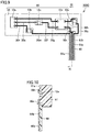
- Fig. 9 is a plan view showing a schematic configuration of an electronic device 100C in embodiment 5.
- Fig. 10 is a cross-sectional view taken along line XI-XI and seen in the arrow direction in Fig. 9 .
- electronic device 100C includes main portion 50, bend portion 60, and interconnection (first interconnection) 30 (30d to 30h, 30m, 30n, 30p).
- An interconnection (second interconnection) 61 (61a to 61c) is formed beforehand on continuous surface 60a of bend portion 60 continuous with upper surface 51a of resin molded body 51.
- Interconnection 61 is made of copper having a thickness of, for example, about 12 ⁇ m.
- interconnection 61 may be made of, for example, aluminum instead of copper.
- Interconnection 30m is connected to interconnection 61c formed on bend portion 60 and is connected to electronic component 12b.
- Interconnection 30n is connected to interconnection 61b formed on bend portion 60 and is connected to electronic component 12d.
- Interconnection 30p is connected to interconnection 61a formed on bend portion 60 and is connected to electronic component 12e.
- bend portion 60 a flexible substrate on which interconnections have already been formed can be used as bend portion 60.
- Electronic device 100C is manufactured in a manufacturing method similar to electronic device 100B in embodiment 4 described above (see Fig. 8 ). However, in the first step shown in Fig. 8 , bend portion 60 is stuck to temporary fixation sheet 200 so that interconnection 61 faces (in contact with) temporary fixation sheet 200. Accordingly, after the injection molding of resin, interconnection 61 is flush with upper surface (sheet bonded surface) 51a of resin molded body 51 that has been in contact with temporary fixation sheet 200. As a result, in forming interconnection 30, a part of interconnection 30 can be easily connected to interconnection 61. Thus, interconnection 61 on bend portion 60 (which is a flexible substrate) can easily be connected to interconnection 30 formed on resin molded body 51. This eliminates the need for conventional complicated processes for connecting a flexible substrate to a rigid substrate, and also eliminates the need for an adhesive or other like members. Thus, the manufacturing cost of electronic device 100C can be reduced.
- 10, 40, 50 main portion; 11, 41, 51: resin molded body; 11a, 41a, 51a: upper surface; 12 (12a to 12e), 42 (42a to 42c), 71, 76a, 76b: electronic component; 13a to 13e, 43a to 43c: electrode; 20, 60: bend portion; 20a, 60a: continuous surface; 30 (30a to 30p), 61 (61a to 61c), 72a, 72b, 77a, 77c: interconnection; 70, 75, 80: substrate; 81: conductive layer; 90a, 90b: conductive adhesive layer; 100, 100A, 100B, 100C: electronic device; 200: temporary fixation sheet; 210: first die; 211: recess; 220: second die; 221, 222: space; 230, 240: structure
Landscapes
- Engineering & Computer Science (AREA)
- Microelectronics & Electronic Packaging (AREA)
- Manufacturing & Machinery (AREA)
- Structure Of Printed Boards (AREA)
- Structures For Mounting Electric Components On Printed Circuit Boards (AREA)
- Encapsulation Of And Coatings For Semiconductor Or Solid State Devices (AREA)
- Structures Or Materials For Encapsulating Or Coating Semiconductor Devices Or Solid State Devices (AREA)
- Production Of Multi-Layered Print Wiring Board (AREA)
Applications Claiming Priority (2)
| Application Number | Priority Date | Filing Date | Title |
|---|---|---|---|
| JP2016226044A JP6776840B2 (ja) | 2016-11-21 | 2016-11-21 | 電子装置およびその製造方法 |
| PCT/JP2017/033675 WO2018092407A1 (ja) | 2016-11-21 | 2017-09-19 | 電子装置およびその製造方法 |
Publications (3)
| Publication Number | Publication Date |
|---|---|
| EP3544392A1 EP3544392A1 (en) | 2019-09-25 |
| EP3544392A4 EP3544392A4 (en) | 2020-01-29 |
| EP3544392B1 true EP3544392B1 (en) | 2021-08-11 |
Family
ID=62146455
Family Applications (1)
| Application Number | Title | Priority Date | Filing Date |
|---|---|---|---|
| EP17871776.5A Active EP3544392B1 (en) | 2016-11-21 | 2017-09-19 | Electronic device and method for producing same |
Country Status (6)
| Country | Link |
|---|---|
| US (1) | US11004699B2 (https=) |
| EP (1) | EP3544392B1 (https=) |
| JP (1) | JP6776840B2 (https=) |
| CN (1) | CN109792836B (https=) |
| TW (1) | TWI660650B (https=) |
| WO (1) | WO2018092407A1 (https=) |
Families Citing this family (3)
| Publication number | Priority date | Publication date | Assignee | Title |
|---|---|---|---|---|
| JP7634555B2 (ja) * | 2020-11-16 | 2025-02-21 | 株式会社フジクラ | 配線板及び配線板の製造方法 |
| JP7286902B1 (ja) * | 2022-05-31 | 2023-06-06 | 眞一 前田 | 電子部品の配線構造、電子部品の接続方法 |
| TWI859865B (zh) | 2023-05-18 | 2024-10-21 | 達運精密工業股份有限公司 | 電子裝置及其製造方法 |
Family Cites Families (24)
| Publication number | Priority date | Publication date | Assignee | Title |
|---|---|---|---|---|
| JPH04346490A (ja) * | 1991-05-24 | 1992-12-02 | Matsushita Electric Ind Co Ltd | プリント配線板の製造方法 |
| JPH06177490A (ja) | 1992-12-03 | 1994-06-24 | Matsushita Electric Works Ltd | プリント配線板 |
| JP4103653B2 (ja) * | 2003-03-27 | 2008-06-18 | 株式会社デンソー | Icカード |
| WO2005004563A1 (ja) | 2003-07-03 | 2005-01-13 | Hitachi, Ltd. | モジュール装置及びその製造方法 |
| JP4602208B2 (ja) * | 2004-12-15 | 2010-12-22 | 新光電気工業株式会社 | 電子部品実装構造体及びその製造方法 |
| US7759167B2 (en) * | 2005-11-23 | 2010-07-20 | Imec | Method for embedding dies |
| JP4920288B2 (ja) | 2005-12-23 | 2012-04-18 | 帝国通信工業株式会社 | 電子部品の回路基板への取付構造及び取付方法 |
| DE102006055576A1 (de) | 2006-11-21 | 2008-05-29 | Fraunhofer-Gesellschaft zur Förderung der angewandten Forschung e.V. | Verfahren zum Herstellen eines dehnbaren Schaltungsträgers und dehnbarer Schaltungsträger |
| JP5089184B2 (ja) * | 2007-01-30 | 2012-12-05 | ローム株式会社 | 樹脂封止型半導体装置およびその製造方法 |
| JP2009071234A (ja) * | 2007-09-18 | 2009-04-02 | Denso Corp | 半導体装置 |
| JP2009147010A (ja) * | 2007-12-12 | 2009-07-02 | Ricoh Co Ltd | 配線構造体 |
| TWI355220B (en) | 2008-07-14 | 2011-12-21 | Unimicron Technology Corp | Circuit board structure |
| JP5374975B2 (ja) * | 2008-09-03 | 2013-12-25 | 住友電気工業株式会社 | シール構造および電子機器 |
| KR101284376B1 (ko) * | 2009-01-27 | 2013-07-09 | 파나소닉 주식회사 | 반도체 칩의 실장 방법, 그 방법을 이용하여 얻어진 반도체 장치 및 반도체 칩의 접속 방법, 및, 표면에 배선이 설치된 입체 구조물 및 그 제법 |
| JP5251845B2 (ja) * | 2009-11-26 | 2013-07-31 | 株式会社安川電機 | 半導体装置の製造方法 |
| US8929085B2 (en) | 2011-09-30 | 2015-01-06 | Apple Inc. | Flexible electronic devices |
| JP5386567B2 (ja) * | 2011-11-15 | 2014-01-15 | 株式会社フジクラ | 撮像素子チップの実装方法、内視鏡の組立方法、撮像モジュール及び内視鏡 |
| CN104380705B (zh) * | 2012-06-29 | 2018-01-19 | 索尼公司 | 相机模块和电子设备 |
| CN205093042U (zh) | 2013-05-13 | 2016-03-16 | 株式会社村田制作所 | 柔性电路基板 |
| JP6354285B2 (ja) | 2014-04-22 | 2018-07-11 | オムロン株式会社 | 電子部品を埋設した樹脂構造体およびその製造方法 |
| US20150359099A1 (en) * | 2014-06-04 | 2015-12-10 | Apple Inc. | Low area over-head connectivity solutions to sip module |
| JP6385234B2 (ja) * | 2014-10-16 | 2018-09-05 | 三菱電機株式会社 | 半導体装置 |
| EP3218928A4 (en) | 2014-11-12 | 2018-09-19 | Intel Corporation | Flexible system-in-package solutions for wearable devices |
| JP2016111037A (ja) * | 2014-12-02 | 2016-06-20 | 東レ株式会社 | 太陽電池裏面保護用シート、およびそれを用いた太陽電池 |
-
2016
- 2016-11-21 JP JP2016226044A patent/JP6776840B2/ja not_active Expired - Fee Related
-
2017
- 2017-09-19 US US16/336,923 patent/US11004699B2/en not_active Expired - Fee Related
- 2017-09-19 EP EP17871776.5A patent/EP3544392B1/en active Active
- 2017-09-19 CN CN201780060052.XA patent/CN109792836B/zh not_active Expired - Fee Related
- 2017-09-19 WO PCT/JP2017/033675 patent/WO2018092407A1/ja not_active Ceased
- 2017-09-27 TW TW106133028A patent/TWI660650B/zh not_active IP Right Cessation
Non-Patent Citations (1)
| Title |
|---|
| None * |
Also Published As
| Publication number | Publication date |
|---|---|
| TW201820943A (zh) | 2018-06-01 |
| TWI660650B (zh) | 2019-05-21 |
| US20200035511A1 (en) | 2020-01-30 |
| WO2018092407A1 (ja) | 2018-05-24 |
| CN109792836B (zh) | 2021-10-15 |
| JP6776840B2 (ja) | 2020-10-28 |
| EP3544392A4 (en) | 2020-01-29 |
| CN109792836A (zh) | 2019-05-21 |
| JP2018085377A (ja) | 2018-05-31 |
| EP3544392A1 (en) | 2019-09-25 |
| US11004699B2 (en) | 2021-05-11 |
Similar Documents
| Publication | Publication Date | Title |
|---|---|---|
| US9922932B2 (en) | Resin structure having electronic component embedded therein, and method for manufacturing said structure | |
| EP3120381B1 (en) | Flexible electronics apparatus and associated methods | |
| US20110019370A1 (en) | Flexible circuit module | |
| EP2519083A1 (en) | Flexible circuit board and manufacturing method thereof | |
| JP7295373B2 (ja) | プリント回路板及びその製造方法 | |
| EP3544392B1 (en) | Electronic device and method for producing same | |
| US20120012369A1 (en) | Circuit board | |
| CN107251664A (zh) | 立体电路构造体 | |
| JP5151025B2 (ja) | フレキシブル回路基板 | |
| WO2019098029A1 (ja) | 電子装置およびその製造方法 | |
| US9265159B2 (en) | Stacked structure and manufacturing method of the same | |
| CN107850803B (zh) | 电子装置及其制造方法 | |
| US10631415B2 (en) | Electronic device and manufacturing method thereof | |
| EP3589089B1 (en) | Electronic device and method for manufacturing same | |
| WO2024201094A1 (en) | Method of forming a functional substrate foil and method of forming a functional substrate | |
| WO2018092408A1 (ja) | 電子装置およびその製造方法 | |
| JP2007019380A (ja) | 回路配線モジュール及び回路配線モジュールの製造方法 |
Legal Events
| Date | Code | Title | Description |
|---|---|---|---|
| STAA | Information on the status of an ep patent application or granted ep patent |
Free format text: STATUS: THE INTERNATIONAL PUBLICATION HAS BEEN MADE |
|
| PUAI | Public reference made under article 153(3) epc to a published international application that has entered the european phase |
Free format text: ORIGINAL CODE: 0009012 |
|
| STAA | Information on the status of an ep patent application or granted ep patent |
Free format text: STATUS: REQUEST FOR EXAMINATION WAS MADE |
|
| 17P | Request for examination filed |
Effective date: 20190326 |
|
| AK | Designated contracting states |
Kind code of ref document: A1 Designated state(s): AL AT BE BG CH CY CZ DE DK EE ES FI FR GB GR HR HU IE IS IT LI LT LU LV MC MK MT NL NO PL PT RO RS SE SI SK SM TR |
|
| AX | Request for extension of the european patent |
Extension state: BA ME |
|
| A4 | Supplementary search report drawn up and despatched |
Effective date: 20200108 |
|
| RIC1 | Information provided on ipc code assigned before grant |
Ipc: H01L 21/56 20060101ALI20191220BHEP Ipc: H05K 1/02 20060101ALI20191220BHEP Ipc: H01L 23/31 20060101AFI20191220BHEP Ipc: H05K 3/00 20060101ALI20191220BHEP Ipc: H01L 23/12 20060101ALI20191220BHEP Ipc: H01L 23/28 20060101ALI20191220BHEP |
|
| DAV | Request for validation of the european patent (deleted) | ||
| DAX | Request for extension of the european patent (deleted) | ||
| STAA | Information on the status of an ep patent application or granted ep patent |
Free format text: STATUS: EXAMINATION IS IN PROGRESS |
|
| 17Q | First examination report despatched |
Effective date: 20200907 |
|
| REG | Reference to a national code |
Ref country code: DE Ref legal event code: R079 Ref document number: 602017044036 Country of ref document: DE Free format text: PREVIOUS MAIN CLASS: H05K0001020000 Ipc: H01L0023310000 |
|
| GRAP | Despatch of communication of intention to grant a patent |
Free format text: ORIGINAL CODE: EPIDOSNIGR1 |
|
| STAA | Information on the status of an ep patent application or granted ep patent |
Free format text: STATUS: GRANT OF PATENT IS INTENDED |
|
| RIC1 | Information provided on ipc code assigned before grant |
Ipc: H01L 25/16 20060101ALN20210409BHEP Ipc: H05K 1/14 20060101ALN20210409BHEP Ipc: H05K 1/02 20060101ALI20210409BHEP Ipc: H05K 3/28 20060101ALI20210409BHEP Ipc: H01L 23/12 20060101ALI20210409BHEP Ipc: H01L 21/56 20060101ALI20210409BHEP Ipc: H01L 23/31 20060101AFI20210409BHEP |
|
| INTG | Intention to grant announced |
Effective date: 20210507 |
|
| RIC1 | Information provided on ipc code assigned before grant |
Ipc: H01L 25/16 20060101ALN20210427BHEP Ipc: H05K 1/14 20060101ALN20210427BHEP Ipc: H05K 1/02 20060101ALI20210427BHEP Ipc: H05K 3/28 20060101ALI20210427BHEP Ipc: H01L 23/12 20060101ALI20210427BHEP Ipc: H01L 21/56 20060101ALI20210427BHEP Ipc: H01L 23/31 20060101AFI20210427BHEP |
|
| GRAS | Grant fee paid |
Free format text: ORIGINAL CODE: EPIDOSNIGR3 |
|
| GRAA | (expected) grant |
Free format text: ORIGINAL CODE: 0009210 |
|
| STAA | Information on the status of an ep patent application or granted ep patent |
Free format text: STATUS: THE PATENT HAS BEEN GRANTED |
|
| AK | Designated contracting states |
Kind code of ref document: B1 Designated state(s): AL AT BE BG CH CY CZ DE DK EE ES FI FR GB GR HR HU IE IS IT LI LT LU LV MC MK MT NL NO PL PT RO RS SE SI SK SM TR |
|
| REG | Reference to a national code |
Ref country code: CH Ref legal event code: EP |
|
| REG | Reference to a national code |
Ref country code: DE Ref legal event code: R096 Ref document number: 602017044036 Country of ref document: DE |
|
| REG | Reference to a national code |
Ref country code: IE Ref legal event code: FG4D Ref country code: AT Ref legal event code: REF Ref document number: 1420270 Country of ref document: AT Kind code of ref document: T Effective date: 20210915 |
|
| REG | Reference to a national code |
Ref country code: LT Ref legal event code: MG9D |
|
| REG | Reference to a national code |
Ref country code: NL Ref legal event code: MP Effective date: 20210811 |
|
| REG | Reference to a national code |
Ref country code: AT Ref legal event code: MK05 Ref document number: 1420270 Country of ref document: AT Kind code of ref document: T Effective date: 20210811 |
|
| PG25 | Lapsed in a contracting state [announced via postgrant information from national office to epo] |
Ref country code: LT Free format text: LAPSE BECAUSE OF FAILURE TO SUBMIT A TRANSLATION OF THE DESCRIPTION OR TO PAY THE FEE WITHIN THE PRESCRIBED TIME-LIMIT Effective date: 20210811 Ref country code: BG Free format text: LAPSE BECAUSE OF FAILURE TO SUBMIT A TRANSLATION OF THE DESCRIPTION OR TO PAY THE FEE WITHIN THE PRESCRIBED TIME-LIMIT Effective date: 20211111 Ref country code: AT Free format text: LAPSE BECAUSE OF FAILURE TO SUBMIT A TRANSLATION OF THE DESCRIPTION OR TO PAY THE FEE WITHIN THE PRESCRIBED TIME-LIMIT Effective date: 20210811 Ref country code: NO Free format text: LAPSE BECAUSE OF FAILURE TO SUBMIT A TRANSLATION OF THE DESCRIPTION OR TO PAY THE FEE WITHIN THE PRESCRIBED TIME-LIMIT Effective date: 20211111 Ref country code: PT Free format text: LAPSE BECAUSE OF FAILURE TO SUBMIT A TRANSLATION OF THE DESCRIPTION OR TO PAY THE FEE WITHIN THE PRESCRIBED TIME-LIMIT Effective date: 20211213 Ref country code: RS Free format text: LAPSE BECAUSE OF FAILURE TO SUBMIT A TRANSLATION OF THE DESCRIPTION OR TO PAY THE FEE WITHIN THE PRESCRIBED TIME-LIMIT Effective date: 20210811 Ref country code: SE Free format text: LAPSE BECAUSE OF FAILURE TO SUBMIT A TRANSLATION OF THE DESCRIPTION OR TO PAY THE FEE WITHIN THE PRESCRIBED TIME-LIMIT Effective date: 20210811 Ref country code: HR Free format text: LAPSE BECAUSE OF FAILURE TO SUBMIT A TRANSLATION OF THE DESCRIPTION OR TO PAY THE FEE WITHIN THE PRESCRIBED TIME-LIMIT Effective date: 20210811 Ref country code: ES Free format text: LAPSE BECAUSE OF FAILURE TO SUBMIT A TRANSLATION OF THE DESCRIPTION OR TO PAY THE FEE WITHIN THE PRESCRIBED TIME-LIMIT Effective date: 20210811 Ref country code: FI Free format text: LAPSE BECAUSE OF FAILURE TO SUBMIT A TRANSLATION OF THE DESCRIPTION OR TO PAY THE FEE WITHIN THE PRESCRIBED TIME-LIMIT Effective date: 20210811 |
|
| PG25 | Lapsed in a contracting state [announced via postgrant information from national office to epo] |
Ref country code: PL Free format text: LAPSE BECAUSE OF FAILURE TO SUBMIT A TRANSLATION OF THE DESCRIPTION OR TO PAY THE FEE WITHIN THE PRESCRIBED TIME-LIMIT Effective date: 20210811 Ref country code: LV Free format text: LAPSE BECAUSE OF FAILURE TO SUBMIT A TRANSLATION OF THE DESCRIPTION OR TO PAY THE FEE WITHIN THE PRESCRIBED TIME-LIMIT Effective date: 20210811 Ref country code: GR Free format text: LAPSE BECAUSE OF FAILURE TO SUBMIT A TRANSLATION OF THE DESCRIPTION OR TO PAY THE FEE WITHIN THE PRESCRIBED TIME-LIMIT Effective date: 20211112 |
|
| PG25 | Lapsed in a contracting state [announced via postgrant information from national office to epo] |
Ref country code: NL Free format text: LAPSE BECAUSE OF FAILURE TO SUBMIT A TRANSLATION OF THE DESCRIPTION OR TO PAY THE FEE WITHIN THE PRESCRIBED TIME-LIMIT Effective date: 20210811 |
|
| PG25 | Lapsed in a contracting state [announced via postgrant information from national office to epo] |
Ref country code: DK Free format text: LAPSE BECAUSE OF FAILURE TO SUBMIT A TRANSLATION OF THE DESCRIPTION OR TO PAY THE FEE WITHIN THE PRESCRIBED TIME-LIMIT Effective date: 20210811 |
|
| REG | Reference to a national code |
Ref country code: CH Ref legal event code: PL |
|
| REG | Reference to a national code |
Ref country code: DE Ref legal event code: R097 Ref document number: 602017044036 Country of ref document: DE |
|
| REG | Reference to a national code |
Ref country code: BE Ref legal event code: MM Effective date: 20210930 |
|
| PG25 | Lapsed in a contracting state [announced via postgrant information from national office to epo] |
Ref country code: SM Free format text: LAPSE BECAUSE OF FAILURE TO SUBMIT A TRANSLATION OF THE DESCRIPTION OR TO PAY THE FEE WITHIN THE PRESCRIBED TIME-LIMIT Effective date: 20210811 Ref country code: SK Free format text: LAPSE BECAUSE OF FAILURE TO SUBMIT A TRANSLATION OF THE DESCRIPTION OR TO PAY THE FEE WITHIN THE PRESCRIBED TIME-LIMIT Effective date: 20210811 Ref country code: RO Free format text: LAPSE BECAUSE OF FAILURE TO SUBMIT A TRANSLATION OF THE DESCRIPTION OR TO PAY THE FEE WITHIN THE PRESCRIBED TIME-LIMIT Effective date: 20210811 Ref country code: MC Free format text: LAPSE BECAUSE OF FAILURE TO SUBMIT A TRANSLATION OF THE DESCRIPTION OR TO PAY THE FEE WITHIN THE PRESCRIBED TIME-LIMIT Effective date: 20210811 Ref country code: EE Free format text: LAPSE BECAUSE OF FAILURE TO SUBMIT A TRANSLATION OF THE DESCRIPTION OR TO PAY THE FEE WITHIN THE PRESCRIBED TIME-LIMIT Effective date: 20210811 Ref country code: CZ Free format text: LAPSE BECAUSE OF FAILURE TO SUBMIT A TRANSLATION OF THE DESCRIPTION OR TO PAY THE FEE WITHIN THE PRESCRIBED TIME-LIMIT Effective date: 20210811 Ref country code: AL Free format text: LAPSE BECAUSE OF FAILURE TO SUBMIT A TRANSLATION OF THE DESCRIPTION OR TO PAY THE FEE WITHIN THE PRESCRIBED TIME-LIMIT Effective date: 20210811 |
|
| PLBE | No opposition filed within time limit |
Free format text: ORIGINAL CODE: 0009261 |
|
| STAA | Information on the status of an ep patent application or granted ep patent |
Free format text: STATUS: NO OPPOSITION FILED WITHIN TIME LIMIT |
|
| 26N | No opposition filed |
Effective date: 20220512 |
|
| GBPC | Gb: european patent ceased through non-payment of renewal fee |
Effective date: 20211111 |
|
| PG25 | Lapsed in a contracting state [announced via postgrant information from national office to epo] |
Ref country code: LU Free format text: LAPSE BECAUSE OF NON-PAYMENT OF DUE FEES Effective date: 20210919 Ref country code: IT Free format text: LAPSE BECAUSE OF FAILURE TO SUBMIT A TRANSLATION OF THE DESCRIPTION OR TO PAY THE FEE WITHIN THE PRESCRIBED TIME-LIMIT Effective date: 20210811 Ref country code: IE Free format text: LAPSE BECAUSE OF NON-PAYMENT OF DUE FEES Effective date: 20210919 Ref country code: BE Free format text: LAPSE BECAUSE OF NON-PAYMENT OF DUE FEES Effective date: 20210930 |
|
| PG25 | Lapsed in a contracting state [announced via postgrant information from national office to epo] |
Ref country code: SI Free format text: LAPSE BECAUSE OF FAILURE TO SUBMIT A TRANSLATION OF THE DESCRIPTION OR TO PAY THE FEE WITHIN THE PRESCRIBED TIME-LIMIT Effective date: 20210811 Ref country code: LI Free format text: LAPSE BECAUSE OF NON-PAYMENT OF DUE FEES Effective date: 20210930 Ref country code: CH Free format text: LAPSE BECAUSE OF NON-PAYMENT OF DUE FEES Effective date: 20210930 |
|
| PG25 | Lapsed in a contracting state [announced via postgrant information from national office to epo] |
Ref country code: FR Free format text: LAPSE BECAUSE OF NON-PAYMENT OF DUE FEES Effective date: 20211011 |
|
| PG25 | Lapsed in a contracting state [announced via postgrant information from national office to epo] |
Ref country code: GB Free format text: LAPSE BECAUSE OF NON-PAYMENT OF DUE FEES Effective date: 20211111 |
|
| PGFP | Annual fee paid to national office [announced via postgrant information from national office to epo] |
Ref country code: DE Payment date: 20220621 Year of fee payment: 6 |
|
| PG25 | Lapsed in a contracting state [announced via postgrant information from national office to epo] |
Ref country code: CY Free format text: LAPSE BECAUSE OF FAILURE TO SUBMIT A TRANSLATION OF THE DESCRIPTION OR TO PAY THE FEE WITHIN THE PRESCRIBED TIME-LIMIT Effective date: 20210811 |
|
| PG25 | Lapsed in a contracting state [announced via postgrant information from national office to epo] |
Ref country code: HU Free format text: LAPSE BECAUSE OF FAILURE TO SUBMIT A TRANSLATION OF THE DESCRIPTION OR TO PAY THE FEE WITHIN THE PRESCRIBED TIME-LIMIT; INVALID AB INITIO Effective date: 20170919 |
|
| REG | Reference to a national code |
Ref country code: DE Ref legal event code: R119 Ref document number: 602017044036 Country of ref document: DE |
|
| PG25 | Lapsed in a contracting state [announced via postgrant information from national office to epo] |
Ref country code: MK Free format text: LAPSE BECAUSE OF FAILURE TO SUBMIT A TRANSLATION OF THE DESCRIPTION OR TO PAY THE FEE WITHIN THE PRESCRIBED TIME-LIMIT Effective date: 20210811 |
|
| PG25 | Lapsed in a contracting state [announced via postgrant information from national office to epo] |
Ref country code: DE Free format text: LAPSE BECAUSE OF NON-PAYMENT OF DUE FEES Effective date: 20240403 |
|
| PG25 | Lapsed in a contracting state [announced via postgrant information from national office to epo] |
Ref country code: MT Free format text: LAPSE BECAUSE OF FAILURE TO SUBMIT A TRANSLATION OF THE DESCRIPTION OR TO PAY THE FEE WITHIN THE PRESCRIBED TIME-LIMIT Effective date: 20210811 |
|
| PG25 | Lapsed in a contracting state [announced via postgrant information from national office to epo] |
Ref country code: TR Free format text: LAPSE BECAUSE OF FAILURE TO SUBMIT A TRANSLATION OF THE DESCRIPTION OR TO PAY THE FEE WITHIN THE PRESCRIBED TIME-LIMIT Effective date: 20210811 |