EP3544182B1 - Taktkompensationsschaltung, taktschaltung und mikrokontroller - Google Patents
Taktkompensationsschaltung, taktschaltung und mikrokontroller Download PDFInfo
- Publication number
- EP3544182B1 EP3544182B1 EP17872201.3A EP17872201A EP3544182B1 EP 3544182 B1 EP3544182 B1 EP 3544182B1 EP 17872201 A EP17872201 A EP 17872201A EP 3544182 B1 EP3544182 B1 EP 3544182B1
- Authority
- EP
- European Patent Office
- Prior art keywords
- circuit
- clock
- value
- digital signal
- module
- Prior art date
- Legal status (The legal status is an assumption and is not a legal conclusion. Google has not performed a legal analysis and makes no representation as to the accuracy of the status listed.)
- Active
Links
Images



Classifications
-
- H—ELECTRICITY
- H03—ELECTRONIC CIRCUITRY
- H03K—PULSE TECHNIQUE
- H03K5/00—Manipulating of pulses not covered by one of the other main groups of this subclass
- H03K5/13—Arrangements having a single output and transforming input signals into pulses delivered at desired time intervals
- H03K5/135—Arrangements having a single output and transforming input signals into pulses delivered at desired time intervals by the use of time reference signals, e.g. clock signals
-
- H—ELECTRICITY
- H03—ELECTRONIC CIRCUITRY
- H03K—PULSE TECHNIQUE
- H03K3/00—Circuits for generating electric pulses; Monostable, bistable or multistable circuits
- H03K3/01—Details
- H03K3/011—Modifications of generator to compensate for variations in physical values, e.g. voltage, temperature
-
- H—ELECTRICITY
- H03—ELECTRONIC CIRCUITRY
- H03K—PULSE TECHNIQUE
- H03K3/00—Circuits for generating electric pulses; Monostable, bistable or multistable circuits
- H03K3/02—Generators characterised by the type of circuit or by the means used for producing pulses
- H03K3/023—Generators characterised by the type of circuit or by the means used for producing pulses by the use of differential amplifiers or comparators, with internal or external positive feedback
- H03K3/0231—Astable circuits
-
- H—ELECTRICITY
- H03—ELECTRONIC CIRCUITRY
- H03B—GENERATION OF OSCILLATIONS, DIRECTLY OR BY FREQUENCY-CHANGING, BY CIRCUITS EMPLOYING ACTIVE ELEMENTS WHICH OPERATE IN A NON-SWITCHING MANNER; GENERATION OF NOISE BY SUCH CIRCUITS
- H03B5/00—Generation of oscillations using amplifier with regenerative feedback from output to input
- H03B5/02—Details
- H03B5/04—Modifications of generator to compensate for variations in physical values, e.g. power supply, load, temperature
-
- H—ELECTRICITY
- H03—ELECTRONIC CIRCUITRY
- H03K—PULSE TECHNIQUE
- H03K4/00—Generating pulses having essentially a finite slope or stepped portions
- H03K4/06—Generating pulses having essentially a finite slope or stepped portions having triangular shape
- H03K4/08—Generating pulses having essentially a finite slope or stepped portions having triangular shape having sawtooth shape
- H03K4/48—Generating pulses having essentially a finite slope or stepped portions having triangular shape having sawtooth shape using as active elements semiconductor devices
- H03K4/50—Generating pulses having essentially a finite slope or stepped portions having triangular shape having sawtooth shape using as active elements semiconductor devices in which a sawtooth voltage is produced across a capacitor
- H03K4/501—Generating pulses having essentially a finite slope or stepped portions having triangular shape having sawtooth shape using as active elements semiconductor devices in which a sawtooth voltage is produced across a capacitor the starting point of the flyback period being determined by the amplitude of the voltage across the capacitor, e.g. by a comparator
- H03K4/502—Generating pulses having essentially a finite slope or stepped portions having triangular shape having sawtooth shape using as active elements semiconductor devices in which a sawtooth voltage is produced across a capacitor the starting point of the flyback period being determined by the amplitude of the voltage across the capacitor, e.g. by a comparator the capacitor being charged from a constant-current source
Definitions
- the present disclosure relates to the field of circuit design, and in particular to a clock compensation circuit, a clock circuit and a microcontroller.
- a clock is taken as an important element in a microcontroller, and its high precision and wide power supply working range are of great significance to improve the performance of a whole chip.
- a Remote Control (RC) clock has a simple structure and is widely applied in an integrated circuit.
- the precision of the RC clock is often limited by the precision of an internal resistor and a capacitor, a power supply and a temperature, and cannot be very high under a full temperature and a full voltage.
- a deviation to the precision of the chip caused by frequency fluctuation of the clock in a full-temperature range and a full-voltage range is even up to ⁇ 2%.
- large-range fluctuation in an environmental temperature and a power voltage of a place where the clock is located causes the fluctuation of a frequency clock, and thus the precision of the microcontroller has a large deviation.
- the document US 6 476 682 B1 discloses a temperature compensated crystal oscillator circuit that utilizes switched capacitor technology wherein all circuitry is contained in a single electronic package, does not need to be calibrated after it leaves manufacturing, and that provides an oscillation frequency with little variation over a wide temperature range,
- a main objective of the present disclosure is to provide a clock compensation circuit, a clock circuit and a microcontroller to solve the problem of large fluctuation of a clock frequency output by a clock circuit in the related art.
- the clock compensation circuit includes a detection circuit and a control circuit.
- the detection circuit is configured to detect a capacitance control parameter capable of affecting a clock frequency output by a clock circuit.
- the control unit is connected with the detection circuit, and is configured to adjust a capacitance value of a target capacitor in the clock circuit according to the capacitance control parameter detected by the detection circuit, so as to change the clock frequency output by the clock circuit.
- the detection circuit may include: a power detection circuit, configured to detect a power voltage of the clock circuit and take the power voltage as the capacitance control parameter.
- control unit may include: a first conversion module, configured to convert an analog signal corresponding to the power voltage detected by the power detection circuit into a first digital signal; a first transmission module, configured to input the first digital signal to a control end of the target capacitor; and a first control module, configured to adjust the capacitance value of the target capacitor according to the first digital signal, so as to change the clock frequency output by the clock circuit.
- the detection circuit includes: a temperature detection circuit, configured to detect an environmental temperature of an environment where the clock circuit is located and take the environmental temperature as the capacitance control parameter.
- control unit includes: a second conversion module, configured to convert an analog signal corresponding to the environmental temperature detected by the temperature detection circuit into a second digital signal; a second transmission module, configured to input the second digital signal to the control end of the target capacitor; and a second control module, configured to adjust the capacitance value of the target capacitor according to the second digital signal, so as to change the clock frequency output by the clock circuit.
- the second control module includes: a first comparison sub-module, configured to compare a value of the detected environmental temperature with a value of a preset temperature; a first adjustment sub-module, configured to decrease, under a condition in which the value of the environmental temperature is smaller than the value of the preset temperature by the comparison, the capacitance value of the target capacitor to a first target capacitance value according to the second digital signal; and a second adjustment sub-module, configured to increase, under a condition in which the value of the environmental temperature is greater than the value of the preset temperature by the comparison, the capacitance value of the target capacitor to a second target capacitance value according to the second digital signal.
- the first control module may include: a second comparison sub-module, configured to compare a value of the power voltage with a value of a preset voltage; a third adjustment sub-module, configured to decrease, under a condition in which the value of the power voltage is smaller than the value of the preset voltage by the comparison, the capacitance value of the target capacitor to a third target capacitance value according to the first digital signal; and a fourth adjustment sub-module, configured to increase, under a condition in which the value of the power voltage is greater than the value of the preset voltage, the capacitance value of the target capacitor to a fourth target capacitance value according to the first digital signal.
- a second comparison sub-module configured to compare a value of the power voltage with a value of a preset voltage
- a third adjustment sub-module configured to decrease, under a condition in which the value of the power voltage is smaller than the value of the preset voltage by the comparison, the capacitance value of the target capacitor to a third target capacitance value according to the
- the detection circuit may further include: a comparator circuit, disposed in the detection circuit, and configured to perform analog-to-digital conversion processing on the capacitance control parameter detected by the detection circuit so as to convert the capacitance control parameter into a corresponding digital signal, where the control unit is configured to adjust the capacitance value of the target capacitor according to the corresponding digital signal to change the clock frequency output by the clock circuit.
- a comparator circuit disposed in the detection circuit, and configured to perform analog-to-digital conversion processing on the capacitance control parameter detected by the detection circuit so as to convert the capacitance control parameter into a corresponding digital signal
- the control unit is configured to adjust the capacitance value of the target capacitor according to the corresponding digital signal to change the clock frequency output by the clock circuit.
- a clock circuit which may include a target capacitor capable of changing a clock frequency output by the clock circuit, and the clock compensation circuit.
- a microcontroller which includes the clock circuit.
- the clock compensation circuit of the present disclosure can compensate the clock circuit according to a demand to reduce the fluctuation of the clock frequency output by the clock circuit.
- a clock compensation circuit According to an embodiment of the present disclosure, there is provided a clock compensation circuit.
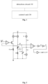
- Fig. 1 is a schematic diagram of a clock compensation circuit provided according to an embodiment of the present disclosure. As shown in Fig. 1 , the clock compensation circuit may include the following structures.
- a detection circuit 10 is configured to detect a capacitance control parameter capable of affecting a clock frequency output by a clock circuit.
- the capacitance control parameter capable of affecting the clock frequency output by the clock circuit is detected by the detection circuit 10 in the clock compensation circuit.
- a target capacitor is disposed in the clock circuit, and its capacitance value is adjustable. The change to the clock frequency output by the clock circuit can be implemented according to a digital signal input to a control end of the target capacitor.
- a control unit 20 is connected with the detection circuit 10, and is configured to adjust the capacitance value of the target capacitor according to the capacitance control parameter detected by the detection circuit 10, so as to change the clock frequency output by the clock circuit.
- the control unit 20 connected with the detection circuit 10 in the clock compensation circuit can adjust the capacitance value of the target capacitor according to the capacitance control parameter detected by the detection circuit 10, and thus changes the clock frequency output by the clock circuit.
- the clock circuit can be compensated according to a demand, and thus the clock frequency output by the clock circuit is changed, and the fluctuation of the clock frequency output by the clock circuit is reduced.
- the detection circuit 10 may include: a power detection circuit 10, configured to detect a power voltage in the clock circuit and take the power voltage as the capacitance control parameter.
- the detection circuit 10 in the clock compensation circuit may include the power detection circuit configured to detect the power voltage of the clock circuit.
- the power detection circuit in the detection circuit 10 detects the power voltage of the clock circuit, and adjusts the capacitance value of the target capacitor according to the power voltage, so as to change the clock frequency output by the clock circuit.
- the control unit 20 may include: a first conversion module, configured to convert an analog signal corresponding to the power voltage detected by the detection circuit 10 (specifically the power detection circuit) into a first digital signal; a first transmission module, configured to input the first digital signal to the control end of the target capacitor; and a first control module, configured to control the capacitance value of the target capacitor according to the first digital signal, so as to change the clock frequency output by the clock circuit.
- a first conversion module configured to convert an analog signal corresponding to the power voltage detected by the detection circuit 10 (specifically the power detection circuit) into a first digital signal
- a first transmission module configured to input the first digital signal to the control end of the target capacitor
- a first control module configured to control the capacitance value of the target capacitor according to the first digital signal, so as to change the clock frequency output by the clock circuit.
- the detection circuit 10 detects that the power voltage of the clock circuit is 5.3V.
- the first conversion module converts the analog signal corresponding to the power voltage detected by the power detection circuit into the first digital signal, i.e., the first conversion module converts the 5.3V into the first digital signal.
- the first control module controls the capacitance value of the target capacitor according to the first digital signal in a circuit where the target capacitor is located so as to change the clock frequency output by the clock circuit. It is to be noted that each figure in the above example is merely for the convenience of description, and does not represent a figure adjusted normally in an actual circuit operation process.
- the first control module may include: a second comparison sub-module, configured to compare a value of the power voltage and a preset voltage; a third adjustment sub-module, configured to decrease, under a condition in which the power voltage is smaller than the preset voltage by the comparison, the capacitance value of the target capacitor to a third target capacitance value according to the first digital signal; and a fourth adjustment sub-module, configured to increase, under a condition in which the value of the power voltage is greater than the value of the preset voltage, the capacitance value of the target capacitor to a fourth target capacitance value according to the first digital signal.
- the power voltage at which the clock circuit operates ranges from 2.7V to 5.5V, and the preset voltage is 5V.
- the second comparison sub-module performs the value comparison on the detected power voltage and the preset voltage.
- the detected power voltage is 4.5V and is smaller than the preset voltage 5V
- the capacitance value of the target capacitor is 110F
- an adjustable range of the target capacitor is 50F-550F
- the third adjustment sub-module decreases the capacitance value 110F of the target capacitor to 100F.
- the fourth adjustment sub-module increases the capacitance value 110F of the target capacitor to 130F.
- the detection circuit 10 further includes: a temperature detection circuit, configured to detect an environmental temperature of an environment where the clock circuit is located and take the environmental temperature as the capacitance control parameter.
- the detection circuit 10 in the clock compensation circuit includes the temperature detection circuit configured to detect the environmental temperature of the environment where the clock circuit is located.
- the control unit controls the target capacitor according to the environmental temperature, detected by the temperature detection circuit, of the environment where the clock circuit is located, so as to change the clock frequency output by the clock circuit.
- control unit 20 further includes: a second conversion module, configured to convert an analog signal corresponding to the environmental temperature detected by the detection circuit 10 into a second digital signal; a second transmission module, configured to input the second digital signal to the control end of the target capacitor; and a second control module, configured to adjust the capacitance value of the target capacitor according to the second digital signal, so as to change the clock frequency output by the clock circuit.
- a mapping relationship between an environmental temperature and a voltage value is established in advance.
- the detection circuit 10 detects that the environmental temperature of the environment where the clock circuit is located is 25°C and the voltage value corresponding to the environmental temperature 25°C is 5V, the detection circuit 10 detects that the environmental temperature of the environment where the clock circuit is located is 26 °C and the voltage value corresponding to the environmental temperature 26°C is 5.1V, and the like.
- the analog signal corresponding to the environmental temperature detected by the temperature detection circuit specifically is an analog signal corresponding to the voltage value that corresponds to the environmental temperature detected by the temperature detection circuit, i.e., the second conversion module converts the analog signal corresponding to the voltage value that corresponds to the environmental temperature detected by the temperature detection circuit into the second digital signal; and the second control module adjusts the capacitance value of the target capacitor according to the second digital signal, so as to change the clock frequency output by the clock circuit.
- the second control module includes: a first comparison sub-module, configured to compare a value of the detected environmental temperature and a preset temperature; a first adjustment sub-module, configured to decrease, under a condition in which the value of the environmental temperature is smaller than the value of the preset temperature, the capacitance value of the target capacitor to a first target capacitance value according to the second digital signal; and a second adjustment sub-module, configured to increase, under a condition in which the value of the environmental temperature is greater than the value of the preset temperature, the capacitance value of the target capacitor to a second target capacitance value according to the second digital signal.
- the environmental temperature of the environment where the clock circuit is located ranges from -40°C to 125°C, and the preset temperature is 25°C.
- the first comparison sub-module compares a value of the detected environmental temperature with a value of a preset temperature. In a case where the detected environmental temperature is 15°C and is smaller than the preset temperature 25°C, and an adjustable range of the target capacitor is 50-550F and the capacitance value of the target capacitor is 110F, under a condition in which the temperature is smaller than the preset temperature by the comparison, the first adjustment sub-module decreases the capacitance value 110F of the target capacitor to 100F.
- the second adjustment sub-module increases the capacitance value 110F of the target capacitor to 130F.
- the detection circuit 10 may further include: a comparator circuit, disposed in the detection circuit 10, and configured to perform analog-to-digital conversion processing on the capacitance control parameter detected by the detection circuit 10 so as to convert the capacitance control parameter into a corresponding digital signal, where the control unit 20 is specifically configured to control the target capacitor according to the corresponding digital signal to change the clock frequency output by the clock circuit.
- a comparator in the comparator circuit converts, according to own characteristics that a high level is output when a potential at a forward input end is higher than a reverse input end, and a low level is output when a potential at the reverse input end is higher than the forward input end, the analog signal detected by the detection circuit 10 and corresponding to the capacitor control parameter into a corresponding digital signal.
- the corresponding digital signal is 101010011; and the control end of the target capacitor is controlled according to this binary code so as to change the clock frequency output by the clock circuit.
- the clock compensation circuit of the present disclosure within a low-voltage range, according to an actual precision demand, a plurality of comparator circuits are increased. Moreover, it is necessary to provide a hysteresis voltage inside each of the comparator circuits, so as to ensure that digital signals are not generated by comparators in a mess. Since the output clock frequency of the clock circuit is in a linear relationship with the environmental temperature, digits controlled digitally are designed on the premise of guaranteeing the precision according to an actual temperature range. With the hysteresis voltages inside the comparator circuits, it is ensured that the digital signals are not generated by the comparators in a mess.
- the detection circuit 10 detects the capacitance control parameter capable of affecting the clock frequency output by the clock circuit, and the control unit 20 adjusts the capacitance value of the target capacitor in the clock circuit according to the capacitance control parameter detected by the detection circuit, so as to change the clock frequency output by the clock circuit, so the problem of large fluctuation of a clock frequency output by a clock circuit in the related art is solved.
- the capacitance value of the target capacitor in the clock circuit is adjusted according to the capacitance control parameter detected by the detection circuit 10, so that the clock frequency output by the clock circuit is changed, and thus the effect of reducing the fluctuation of the clock frequency output by the clock circuit is achieved.
- Fig. 2 is a structural diagram of a clock circuit in the related art. As shown in Fig. 2 , a structural diagram of a clock circuit inside a chip having a universal structure is shown in Fig. 2 . A current bias in a direct proportion to a reference current source at 1: M is applied to branches of an R trim and an R 0 .
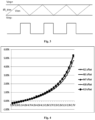
- Fig. 3 is a working principle diagram of a clock circuit in the related art. As shown in Fig.
- a generated voltage bias (V inp+ and V inp- ) jumped along with the clock is applied to one end of a high-speed comparator; the other end of the high-speed comparator charges and discharges a capacitor according to two switchable current sources to obtain a zigzag wave voltage V im .
- the voltages at two ends pass through the high-speed comparator to obtain a square wave clock. Since a capacitance and a resistance in a process when a chip is manufactured actually may have a 20% deviation at most compared with ideal nominal capacitance value and resistance value, it is very difficult that an internal clock circuit made actually reaches a very high precision if there is no calibration circuit. Moreover, even through the internal calibration circuit exists, an about 5% deviation may also be generated due to different working voltages and temperatures of places where the chip is located.
- Fig. 4 is a schematic diagram of a frequency change of a clock circuit in a full-voltage range in the related art. It may be seen from actual test results in Fig. 4 that an output frequency may not be in a linear relationship with a power voltage, but change violently within a range in which the power voltage is low. From Fig. 4 , because of the change of the power voltage in a full-voltage range, the output frequency changes about 5%.
- Fig. 5 is a schematic diagram of a frequency change of a clock circuit in a full-temperature range in the related art. As shown in Fig. 5 , an output frequency is in a linear relationship with an environmental temperature. Because of the change of the power voltage in a full-temperature range, the output frequency changes about ⁇ 2.5%.
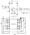
- Fig. 6 is a structural diagram of a clock circuit provided according to an embodiment of the present disclosure.
- the detection circuit in the present disclosure is increased to the circuit in Fig. 6 .
- a power detection circuit is increased to detect the power voltage, convert an analog signal corresponding to the power voltage into a binary code (a digital signal corresponding to the analog signal), apply the binary code (the digital signal corresponding to the analog signal) to a C_trim circuit, and control a magnitude of a capacitor connected inside a system loop to adjust an output frequency of the circuit, thereby achieving the effect of automatically compensating the power voltage.
- Fig. 7 is a schematic diagram of a frequency change of a clock circuit in a full-voltage range provided according to an embodiment of the present disclosure. It may be seen from actual test results in Fig. 7 that the change in a range in which the power voltage is low is stable; and in a full-voltage range, because of the change of the power voltage, the output frequency changes about ⁇ 0.6%. In other words, the power voltage of the clock circuit is compensated automatically, so that the clock frequency output by the clock circuit is adjusted, and the fluctuation of the clock frequency output by the clock circuit is reduced.
- An embodiment of the present disclosure further provides a clock circuit.
- the clock circuit may include a target capacitor capable of changing a clock frequency output by the clock circuit, and any clock compensation circuit provided by the embodiments of the present disclosure.
- the clock circuit of the any clock compensation circuit provided by the present disclosure by adjusting the clock frequency output by the clock circuit, the fluctuation of the clock frequency is reduced, and thus the effect of reducing a deviation of the precision of a microcontroller is achieved, and the effect of reducing the fluctuation of the clock frequency output by the clock circuit is achieved.
- An embodiment of the present disclosure further provides a microcontroller.
- the microcontroller includes a clock circuit provided by the embodiments of the present disclosure.
- the microcontroller provided by the present disclosure by adjusting the clock frequency output by the clock circuit, the fluctuation of the clock frequency output by the clock circuit is reduced, and thus the effect of reducing a deviation of the precision of a microcontroller is achieved, and the effect of reducing the fluctuation of the clock frequency output by the clock circuit is achieved.
- each function module in each embodiment of the present disclosure may be integrated into a processing module, each module may also exist independently, and two or more than two module may also be integrated into a module.
- the integrated module may be implemented in a hardware form, and may also be implemented in form of hardware and software function module.
- each module of the present disclosure may be implemented by a universal computing device, and the modules may be concentrated on a single computing device or distributed on a network formed by a plurality of computing devices, and may optionally be implemented by program codes executable for the computing devices, so that the modules may be stored in a storage device for execution with the computing devices, the shown or described steps may be executed in sequences different from those described here in some circumstances, or may form each integrated circuit module respectively, or multiple modules therein may form a single integrated circuit module for implementation. Therefore, the present disclosure is not limited to any specific hardware and software combination.
Landscapes
- Physics & Mathematics (AREA)
- Nonlinear Science (AREA)
- Oscillators With Electromechanical Resonators (AREA)
- Semiconductor Integrated Circuits (AREA)
- Logic Circuits (AREA)
Claims (7)
- Taktkompensationsschaltung, umfassend:eine Erfassungsschaltung, (10), die dazu konfiguriert ist, einen Kapazitätssteuerparameter zu erfassen, der dazu in der Lage ist, eine Taktfrequenz (CLK_OUT) zu beeinflussen, die durch eine Taktschaltung ausgegeben wird; undeine Steuereinheit (20), die mit der Erfassungsschaltung verbunden ist und dazu konfiguriert ist, einen Kapazitätswert eines Zielkondensators (C_trim) in der Taktschaltung gemäß dem Kapazitätssteuerparameter, der durch die Erfassungsschaltung erfasst wird, anzupassen, um die Taktfrequenz zu ändern, die durch die Taktschaltung ausgegeben wird;wobei die Erfassungsschaltung ferner Folgendes umfasst:
eine Temperaturerfassungsschaltung (Temperature sense), die dazu konfiguriert ist, eine Umgebungstemperatur einer Umgebung, in der sich die Taktschaltung befindet, zu erfassen und die Umgebungstemperatur als den Kapazitätssteuerparameter zu übernehmen;die Steuereinheit (20) ferner Folgendes umfasst:ein zweites Umwandlungsmodul, das dazu konfiguriert ist, ein analoges Signal, das der Umgebungstemperatur entspricht, die durch die Temperaturerfassungsschaltung erfasst wird, in ein zweites digitales Signal umzuwandeln;ein zweites Übertragungsmodul, das dazu konfiguriert ist, das zweite digitale Signal in das Steuerende des Zielkondensators einzugeben; undein zweites Steuermodul, das dazu konfiguriert ist, den Kapazitätswert des Zielkondensators gemäß dem zweiten digitalen Signal anzupassen, um die Taktfrequenz zu ändern, die durch die Taktschaltung ausgegeben wird;wobei eine Zuordnungsbeziehung zwischen einer Umgebungstemperatur und einem Spannungswert hergestellt wird, wobei das zweite Umwandlungsmodul dazu konfiguriert ist, das analoge Signal, das dem Spannungswert entspricht, welcher der Umgebungstemperatur entspricht, die durch die Temperaturerfassungsschaltung erfasst wird, in das zweite digitale Signal umzuwandeln;dadurch gekennzeichnet, dass:
das zweite Steuermodul Folgendes umfasst:ein erstes Vergleichsuntermodul, das dazu konfiguriert ist, einen Wert der erfassten Umgebungstemperatur mit einem Wert einer voreingestellten Temperatur zu vergleichen;ein erstes Anpassungsuntermodul, das dazu konfiguriert ist, unter einer Bedingung, bei welcher der Wert der Umgebungstemperatur kleiner als der Wert der voreingestellten Temperatur ist, den Kapazitätswert des Zielkondensators auf einen ersten Zielkapazitätswert gemäß dem zweiten digitalen Signal zu verringern; undein zweites Anpassungsuntermodul, das dazu konfiguriert ist, unter einer Bedingung, bei welcher der Wert der Umgebungstemperatur größer als der Wert der voreingestellten Temperatur ist, den Kapazitätswert des Zielkondensators auf einen zweiten Zielkapazitätswert gemäß dem zweiten digitalen Signal zu erhöhen. - Schaltung nach Anspruch 1, wobei die Erfassungsschaltung (10) Folgendes umfasst:
eine Leistungserfassungsschaltung (Power sense), die dazu konfiguriert ist, eine Leistungsspannung der Taktschaltung zu erfassen und die Leistungsspannung als den Kapazitätssteuerparameter zu übernehmen. - Schaltung nach Anspruch 2, wobei die Steuereinheit Folgendes umfasst:ein erstes Umwandlungsmodul, das dazu konfiguriert ist, ein analoges Signal, das der Leistungsspannung entspricht, die durch die Leistungserfassungsschaltung erfasst wird, in ein erstes digitales Signal umzuwandeln;ein erstes Übertragungsmodul, das dazu konfiguriert ist, das erste digitale Signal in ein Steuerende des Zielkondensators einzugeben; undein erstes Steuermodul, das dazu konfiguriert ist, einen Kapazitätswert des Zielkondensators gemäß dem ersten digitalen Signal anzupassen, um die Taktfrequenz zu ändern, die durch die Taktschaltung ausgegeben wird.
- Schaltung nach Anspruch 3, wobei das erste Steuermodul Folgendes umfasst:ein zweites Vergleichsuntermodul, das dazu konfiguriert ist, einen Wert der Leistungsspannung mit einem Wert einer voreingestellten Spannung zu vergleichen;ein drittes Anpassungsuntermodul, das dazu konfiguriert ist, unter einer Bedingung, bei welcher der Wert der Leistungsspannung kleiner als der Wert der voreingestellten Spannung ist, den Kapazitätswert des Zielkondensators auf einen dritten Zielkapazitätswert gemäß dem ersten digitalen Signal zu verringern; undein viertes Anpassungsuntermodul, das dazu konfiguriert ist, unter einer Bedingung, bei welcher der Wert der Leistungsspannung größer als der Wert der voreingestellten Spannung ist, den Kapazitätswert des Zielkondensators auf einen vierten Zielkapazitätswert gemäß dem ersten digitalen Signal zu erhöhen.
- Schaltung nach Anspruch 1, wobei die Erfassungsschaltung ferner Folgendes umfasst:eine Vergleicherschaltung, die in der Erfassungsschaltung angeordnet ist und dazu konfiguriert ist, eine Analog-Digital-Umwandlungsverarbeitung an dem Kapazitätssteuerparameter durchzuführen, der durch die Erfassungsschaltung erfasst wird, um den Kapazitätssteuerparameter in ein entsprechendes digitales Signal umzuwandeln,wobei die Steuereinheit dazu konfiguriert ist, den Kapazitätswert des Zielkondensators gemäß dem entsprechenden digitalen Signal anzupassen, um die Taktfrequenz zu ändern, die durch die Taktschaltung ausgegeben wird.
- Taktschaltung, umfassend einen Zielkondensator, der dazu in der Lage ist, eine Taktfrequenz zu ändern, die durch die Taktschaltung ausgegeben wird, und die Taktkompensationsschaltung nach Anspruch 1.
- Mikrokontroller, umfassend die Taktschaltung nach Anspruch 6.
Applications Claiming Priority (2)
| Application Number | Priority Date | Filing Date | Title |
|---|---|---|---|
| CN201611015057.4A CN106656120B (zh) | 2016-11-18 | 2016-11-18 | 时钟补偿电路、时钟电路和微控制器 |
| PCT/CN2017/092482 WO2018090650A1 (zh) | 2016-11-18 | 2017-07-11 | 时钟补偿电路、时钟电路和微控制器 |
Publications (3)
| Publication Number | Publication Date |
|---|---|
| EP3544182A1 EP3544182A1 (de) | 2019-09-25 |
| EP3544182A4 EP3544182A4 (de) | 2020-07-29 |
| EP3544182B1 true EP3544182B1 (de) | 2025-02-26 |
Family
ID=58807513
Family Applications (1)
| Application Number | Title | Priority Date | Filing Date |
|---|---|---|---|
| EP17872201.3A Active EP3544182B1 (de) | 2016-11-18 | 2017-07-11 | Taktkompensationsschaltung, taktschaltung und mikrokontroller |
Country Status (6)
| Country | Link |
|---|---|
| US (1) | US10644684B2 (de) |
| EP (1) | EP3544182B1 (de) |
| JP (1) | JP6728475B2 (de) |
| KR (1) | KR102158947B1 (de) |
| CN (1) | CN106656120B (de) |
| WO (1) | WO2018090650A1 (de) |
Families Citing this family (5)
| Publication number | Priority date | Publication date | Assignee | Title |
|---|---|---|---|---|
| CN106656120B (zh) | 2016-11-18 | 2019-09-20 | 珠海格力电器股份有限公司 | 时钟补偿电路、时钟电路和微控制器 |
| KR102271363B1 (ko) | 2019-11-01 | 2021-07-01 | 국방과학연구소 | 클럭 주파수 검출 장치 및 방법 |
| CN111665431B (zh) * | 2020-04-26 | 2023-07-25 | 江西联智集成电路有限公司 | 芯片内部时钟源校准方法、装置、设备及介质 |
| WO2022257028A1 (zh) * | 2021-06-08 | 2022-12-15 | 深圳市汇顶科技股份有限公司 | 时钟校准方法、装置和电子设备 |
| CN114389580B (zh) * | 2021-12-27 | 2025-09-16 | 芯海科技(深圳)股份有限公司 | 电阻模块、时钟电路、集成电路以及电子设备 |
Family Cites Families (18)
| Publication number | Priority date | Publication date | Assignee | Title |
|---|---|---|---|---|
| JPS58111529A (ja) * | 1981-12-25 | 1983-07-02 | Hitachi Ltd | A/d変換器 |
| JPS59119921A (ja) * | 1982-12-25 | 1984-07-11 | Toshiba Corp | アナログ・デイジタル変換器 |
| US5994970A (en) * | 1998-03-23 | 1999-11-30 | Dallas Semiconductor Corporation | Temperature compensated crystal oscillator |
| KR100486461B1 (ko) * | 2002-12-26 | 2005-05-03 | 주식회사 엑사이엔씨 | 다기능 수정발진기 |
| KR100691346B1 (ko) * | 2005-07-06 | 2007-03-12 | 삼성전자주식회사 | 발진기 및 그 보상 방법 |
| JP4960750B2 (ja) * | 2007-04-17 | 2012-06-27 | パナソニック株式会社 | 警報装置 |
| CN101436851A (zh) * | 2007-11-16 | 2009-05-20 | 安凡微电子(上海)有限公司 | 补偿电路和方法、应用该补偿电路的滤波器 |
| JP2011166473A (ja) * | 2010-02-10 | 2011-08-25 | Seiko Epson Corp | 半導体集積回路 |
| JP5451541B2 (ja) * | 2010-06-28 | 2014-03-26 | スパンション エルエルシー | 発振回路 |
| US8248113B2 (en) * | 2010-08-23 | 2012-08-21 | Realtek Semiconductor Corp. | Method and apparatus for accurate clock synthesis |
| CN102571080A (zh) * | 2010-12-27 | 2012-07-11 | 北京中电华大电子设计有限责任公司 | 一种支持动态校准的时钟恢复方法和电路 |
| CN102694523A (zh) * | 2011-03-25 | 2012-09-26 | 鸿富锦精密工业(深圳)有限公司 | 晶振电路 |
| CN102594345B (zh) * | 2012-02-21 | 2014-04-09 | 无锡泽太微电子有限公司 | 一种基于芯片的数据发送方法及系统 |
| JP6245424B2 (ja) * | 2013-08-08 | 2017-12-13 | セイコーエプソン株式会社 | 発振回路の制御方法、発振用回路、発振器、電子機器及び移動体 |
| CN103873048B (zh) | 2014-03-12 | 2017-02-01 | 无锡中科微电子工业技术研究院有限责任公司 | 具有频率自校准功能的片上rc振荡器及频率自校准方法 |
| CN104807561B (zh) | 2015-04-29 | 2017-11-28 | 清华大学深圳研究生院 | 电阻型温度传感芯片的校准电路和校准方法 |
| CN106656120B (zh) * | 2016-11-18 | 2019-09-20 | 珠海格力电器股份有限公司 | 时钟补偿电路、时钟电路和微控制器 |
| KR102749169B1 (ko) * | 2017-01-10 | 2025-01-06 | 삼성전자주식회사 | 온도 보상 발진 제어기 및 그것을 포함하는 온도 보상 수정 발진기 |
-
2016
- 2016-11-18 CN CN201611015057.4A patent/CN106656120B/zh active Active
-
2017
- 2017-07-11 JP JP2019506097A patent/JP6728475B2/ja active Active
- 2017-07-11 US US16/331,057 patent/US10644684B2/en active Active
- 2017-07-11 EP EP17872201.3A patent/EP3544182B1/de active Active
- 2017-07-11 KR KR1020197003201A patent/KR102158947B1/ko active Active
- 2017-07-11 WO PCT/CN2017/092482 patent/WO2018090650A1/zh not_active Ceased
Non-Patent Citations (1)
| Title |
|---|
| "Performance Optimization Techniques in Analog, Mixed-Signal, and Radio-Frequency Circuit Design :", 15 April 2015, IGI GLOBAL, ISBN: 978-1-4666-6628-3, ISSN: 2327-039X, article GUPTA YOGENDRA ET AL: "Thermometer to Gray Encoders : :", pages: 323 - 335, XP093151477, DOI: 10.4018/978-1-4666-6627-6.ch013 * |
Also Published As
| Publication number | Publication date |
|---|---|
| CN106656120B (zh) | 2019-09-20 |
| EP3544182A4 (de) | 2020-07-29 |
| JP6728475B2 (ja) | 2020-07-22 |
| EP3544182A1 (de) | 2019-09-25 |
| US10644684B2 (en) | 2020-05-05 |
| CN106656120A (zh) | 2017-05-10 |
| KR20190022864A (ko) | 2019-03-06 |
| US20190267976A1 (en) | 2019-08-29 |
| KR102158947B1 (ko) | 2020-09-23 |
| JP2019523616A (ja) | 2019-08-22 |
| WO2018090650A1 (zh) | 2018-05-24 |
Similar Documents
| Publication | Publication Date | Title |
|---|---|---|
| US10644684B2 (en) | Clock compensation circuit, clock circuit, and microcontroller | |
| US9634558B2 (en) | Negative charge pump feedback circuit | |
| US9946290B2 (en) | Current reference circuit and an electronic device including the same | |
| US7990184B2 (en) | Comparing device having hysteresis characteristics and voltage regulator using the same | |
| US9780737B1 (en) | Digitally-controlled transimpedance amplifier (TIA) circuit and methods | |
| US9454172B2 (en) | Voltage control circuit with temperature compensation function | |
| US9356506B1 (en) | Charge pump regulator and control method thereof | |
| CN105958943A (zh) | 弛张振荡器 | |
| US20150346749A1 (en) | System and Method for a Linear Voltage Regulator | |
| US20220239284A1 (en) | Clock generation circuits and methods of generating clock signals | |
| US9847178B2 (en) | BST capacitor control | |
| US8030978B2 (en) | Soft-start circuit | |
| EP3072236A1 (de) | Vorrichtung und verfahren zur erzeugung eines temperaturabhängigen steuersignals | |
| KR101514459B1 (ko) | 볼티지 레귤레이터 | |
| EP2099184B1 (de) | Verstärkeranordnung und Signalerzeugungsverfahren | |
| US6172543B1 (en) | 90° phase shift circuit | |
| CN216052961U (zh) | 一种掉电时序控制电路 | |
| EP2439846A1 (de) | Temperaturkompensierter RC-Oszillator | |
| KR101517389B1 (ko) | Rc 자동 교정 시스템 그 교정 방법 | |
| US9093961B2 (en) | Operational amplifier | |
| US20120013414A1 (en) | Crystal oscillator circuit for adjusting resonant frequency of crystal oscillator | |
| WO2017046072A1 (en) | Glitch compensation in electronic circuits | |
| US9647651B2 (en) | Delay circuit and semiconductor device | |
| US20230361764A1 (en) | Power management integrated circuit | |
| US10581414B2 (en) | Semiconductor integrated circuit device |
Legal Events
| Date | Code | Title | Description |
|---|---|---|---|
| STAA | Information on the status of an ep patent application or granted ep patent |
Free format text: STATUS: THE INTERNATIONAL PUBLICATION HAS BEEN MADE |
|
| PUAI | Public reference made under article 153(3) epc to a published international application that has entered the european phase |
Free format text: ORIGINAL CODE: 0009012 |
|
| STAA | Information on the status of an ep patent application or granted ep patent |
Free format text: STATUS: REQUEST FOR EXAMINATION WAS MADE |
|
| 17P | Request for examination filed |
Effective date: 20190311 |
|
| AK | Designated contracting states |
Kind code of ref document: A1 Designated state(s): AL AT BE BG CH CY CZ DE DK EE ES FI FR GB GR HR HU IE IS IT LI LT LU LV MC MK MT NL NO PL PT RO RS SE SI SK SM TR |
|
| AX | Request for extension of the european patent |
Extension state: BA ME |
|
| DAV | Request for validation of the european patent (deleted) | ||
| DAX | Request for extension of the european patent (deleted) | ||
| REG | Reference to a national code |
Ref country code: DE Ref legal event code: R079 Free format text: PREVIOUS MAIN CLASS: H03K0005135000 Ipc: H03K0003011000 |
|
| A4 | Supplementary search report drawn up and despatched |
Effective date: 20200630 |
|
| RIC1 | Information provided on ipc code assigned before grant |
Ipc: H03K 3/0231 20060101ALI20200624BHEP Ipc: H03K 4/502 20060101ALN20200624BHEP Ipc: H03K 3/011 20060101AFI20200624BHEP |
|
| STAA | Information on the status of an ep patent application or granted ep patent |
Free format text: STATUS: EXAMINATION IS IN PROGRESS |
|
| 17Q | First examination report despatched |
Effective date: 20210802 |
|
| P01 | Opt-out of the competence of the unified patent court (upc) registered |
Effective date: 20230530 |
|
| GRAP | Despatch of communication of intention to grant a patent |
Free format text: ORIGINAL CODE: EPIDOSNIGR1 |
|
| STAA | Information on the status of an ep patent application or granted ep patent |
Free format text: STATUS: GRANT OF PATENT IS INTENDED |
|
| RIC1 | Information provided on ipc code assigned before grant |
Ipc: H03K 4/502 20060101ALN20241107BHEP Ipc: H03K 3/0231 20060101ALI20241107BHEP Ipc: H03K 3/011 20060101AFI20241107BHEP |
|
| INTG | Intention to grant announced |
Effective date: 20241211 |
|
| GRAS | Grant fee paid |
Free format text: ORIGINAL CODE: EPIDOSNIGR3 |
|
| GRAA | (expected) grant |
Free format text: ORIGINAL CODE: 0009210 |
|
| STAA | Information on the status of an ep patent application or granted ep patent |
Free format text: STATUS: THE PATENT HAS BEEN GRANTED |
|
| AK | Designated contracting states |
Kind code of ref document: B1 Designated state(s): AL AT BE BG CH CY CZ DE DK EE ES FI FR GB GR HR HU IE IS IT LI LT LU LV MC MK MT NL NO PL PT RO RS SE SI SK SM TR |
|
| REG | Reference to a national code |
Ref country code: GB Ref legal event code: FG4D |
|
| REG | Reference to a national code |
Ref country code: CH Ref legal event code: EP |
|
| REG | Reference to a national code |
Ref country code: DE Ref legal event code: R096 Ref document number: 602017088056 Country of ref document: DE |
|
| REG | Reference to a national code |
Ref country code: IE Ref legal event code: FG4D |
|
| REG | Reference to a national code |
Ref country code: NL Ref legal event code: FP |
|
| PG25 | Lapsed in a contracting state [announced via postgrant information from national office to epo] |
Ref country code: RS Free format text: LAPSE BECAUSE OF FAILURE TO SUBMIT A TRANSLATION OF THE DESCRIPTION OR TO PAY THE FEE WITHIN THE PRESCRIBED TIME-LIMIT Effective date: 20250526 |
|
| PG25 | Lapsed in a contracting state [announced via postgrant information from national office to epo] |
Ref country code: FI Free format text: LAPSE BECAUSE OF FAILURE TO SUBMIT A TRANSLATION OF THE DESCRIPTION OR TO PAY THE FEE WITHIN THE PRESCRIBED TIME-LIMIT Effective date: 20250226 |
|
| PG25 | Lapsed in a contracting state [announced via postgrant information from national office to epo] |
Ref country code: PL Free format text: LAPSE BECAUSE OF FAILURE TO SUBMIT A TRANSLATION OF THE DESCRIPTION OR TO PAY THE FEE WITHIN THE PRESCRIBED TIME-LIMIT Effective date: 20250226 |
|
| PG25 | Lapsed in a contracting state [announced via postgrant information from national office to epo] |
Ref country code: ES Free format text: LAPSE BECAUSE OF FAILURE TO SUBMIT A TRANSLATION OF THE DESCRIPTION OR TO PAY THE FEE WITHIN THE PRESCRIBED TIME-LIMIT Effective date: 20250226 |
|
| REG | Reference to a national code |
Ref country code: LT Ref legal event code: MG9D |
|
| PG25 | Lapsed in a contracting state [announced via postgrant information from national office to epo] |
Ref country code: NO Free format text: LAPSE BECAUSE OF FAILURE TO SUBMIT A TRANSLATION OF THE DESCRIPTION OR TO PAY THE FEE WITHIN THE PRESCRIBED TIME-LIMIT Effective date: 20250526 Ref country code: IS Free format text: LAPSE BECAUSE OF FAILURE TO SUBMIT A TRANSLATION OF THE DESCRIPTION OR TO PAY THE FEE WITHIN THE PRESCRIBED TIME-LIMIT Effective date: 20250626 |
|
| PG25 | Lapsed in a contracting state [announced via postgrant information from national office to epo] |
Ref country code: HR Free format text: LAPSE BECAUSE OF FAILURE TO SUBMIT A TRANSLATION OF THE DESCRIPTION OR TO PAY THE FEE WITHIN THE PRESCRIBED TIME-LIMIT Effective date: 20250226 |
|
| PG25 | Lapsed in a contracting state [announced via postgrant information from national office to epo] |
Ref country code: LV Free format text: LAPSE BECAUSE OF FAILURE TO SUBMIT A TRANSLATION OF THE DESCRIPTION OR TO PAY THE FEE WITHIN THE PRESCRIBED TIME-LIMIT Effective date: 20250226 Ref country code: PT Free format text: LAPSE BECAUSE OF FAILURE TO SUBMIT A TRANSLATION OF THE DESCRIPTION OR TO PAY THE FEE WITHIN THE PRESCRIBED TIME-LIMIT Effective date: 20250626 |
|
| PG25 | Lapsed in a contracting state [announced via postgrant information from national office to epo] |
Ref country code: BG Free format text: LAPSE BECAUSE OF FAILURE TO SUBMIT A TRANSLATION OF THE DESCRIPTION OR TO PAY THE FEE WITHIN THE PRESCRIBED TIME-LIMIT Effective date: 20250226 Ref country code: GR Free format text: LAPSE BECAUSE OF FAILURE TO SUBMIT A TRANSLATION OF THE DESCRIPTION OR TO PAY THE FEE WITHIN THE PRESCRIBED TIME-LIMIT Effective date: 20250527 |
|
| REG | Reference to a national code |
Ref country code: AT Ref legal event code: MK05 Ref document number: 1771676 Country of ref document: AT Kind code of ref document: T Effective date: 20250226 |
|
| PGFP | Annual fee paid to national office [announced via postgrant information from national office to epo] |
Ref country code: NL Payment date: 20250728 Year of fee payment: 9 |
|
| PG25 | Lapsed in a contracting state [announced via postgrant information from national office to epo] |
Ref country code: SE Free format text: LAPSE BECAUSE OF FAILURE TO SUBMIT A TRANSLATION OF THE DESCRIPTION OR TO PAY THE FEE WITHIN THE PRESCRIBED TIME-LIMIT Effective date: 20250226 |
|
| PG25 | Lapsed in a contracting state [announced via postgrant information from national office to epo] |
Ref country code: SM Free format text: LAPSE BECAUSE OF FAILURE TO SUBMIT A TRANSLATION OF THE DESCRIPTION OR TO PAY THE FEE WITHIN THE PRESCRIBED TIME-LIMIT Effective date: 20250226 |
|
| PG25 | Lapsed in a contracting state [announced via postgrant information from national office to epo] |
Ref country code: DK Free format text: LAPSE BECAUSE OF FAILURE TO SUBMIT A TRANSLATION OF THE DESCRIPTION OR TO PAY THE FEE WITHIN THE PRESCRIBED TIME-LIMIT Effective date: 20250226 |
|
| PGFP | Annual fee paid to national office [announced via postgrant information from national office to epo] |
Ref country code: DE Payment date: 20250825 Year of fee payment: 9 |
|
| PGFP | Annual fee paid to national office [announced via postgrant information from national office to epo] |
Ref country code: IT Payment date: 20250725 Year of fee payment: 9 |
|
| PGFP | Annual fee paid to national office [announced via postgrant information from national office to epo] |
Ref country code: GB Payment date: 20250729 Year of fee payment: 9 |
|
| PG25 | Lapsed in a contracting state [announced via postgrant information from national office to epo] |
Ref country code: AT Free format text: LAPSE BECAUSE OF FAILURE TO SUBMIT A TRANSLATION OF THE DESCRIPTION OR TO PAY THE FEE WITHIN THE PRESCRIBED TIME-LIMIT Effective date: 20250226 |
|
| PGFP | Annual fee paid to national office [announced via postgrant information from national office to epo] |
Ref country code: FR Payment date: 20250729 Year of fee payment: 9 |
|
| PGFP | Annual fee paid to national office [announced via postgrant information from national office to epo] |
Ref country code: CH Payment date: 20250801 Year of fee payment: 9 |
|
| PG25 | Lapsed in a contracting state [announced via postgrant information from national office to epo] |
Ref country code: EE Free format text: LAPSE BECAUSE OF FAILURE TO SUBMIT A TRANSLATION OF THE DESCRIPTION OR TO PAY THE FEE WITHIN THE PRESCRIBED TIME-LIMIT Effective date: 20250226 Ref country code: CZ Free format text: LAPSE BECAUSE OF FAILURE TO SUBMIT A TRANSLATION OF THE DESCRIPTION OR TO PAY THE FEE WITHIN THE PRESCRIBED TIME-LIMIT Effective date: 20250226 |
|
| PG25 | Lapsed in a contracting state [announced via postgrant information from national office to epo] |
Ref country code: RO Free format text: LAPSE BECAUSE OF FAILURE TO SUBMIT A TRANSLATION OF THE DESCRIPTION OR TO PAY THE FEE WITHIN THE PRESCRIBED TIME-LIMIT Effective date: 20250226 |
|
| PG25 | Lapsed in a contracting state [announced via postgrant information from national office to epo] |
Ref country code: SK Free format text: LAPSE BECAUSE OF FAILURE TO SUBMIT A TRANSLATION OF THE DESCRIPTION OR TO PAY THE FEE WITHIN THE PRESCRIBED TIME-LIMIT Effective date: 20250226 |
|
| REG | Reference to a national code |
Ref country code: DE Ref legal event code: R097 Ref document number: 602017088056 Country of ref document: DE |
|
| PLBE | No opposition filed within time limit |
Free format text: ORIGINAL CODE: 0009261 |
|
| STAA | Information on the status of an ep patent application or granted ep patent |
Free format text: STATUS: NO OPPOSITION FILED WITHIN TIME LIMIT |
|
| 26N | No opposition filed |
Effective date: 20251127 |
|
| PG25 | Lapsed in a contracting state [announced via postgrant information from national office to epo] |
Ref country code: LU Free format text: LAPSE BECAUSE OF NON-PAYMENT OF DUE FEES Effective date: 20250711 |
|
| REG | Reference to a national code |
Ref country code: BE Ref legal event code: MM Effective date: 20250731 |
|
| PG25 | Lapsed in a contracting state [announced via postgrant information from national office to epo] |
Ref country code: BE Free format text: LAPSE BECAUSE OF NON-PAYMENT OF DUE FEES Effective date: 20250731 |