EP3531460B1 - Composant piézoélectrique et tête d'éjection de liquide - Google Patents
Composant piézoélectrique et tête d'éjection de liquide Download PDFInfo
- Publication number
- EP3531460B1 EP3531460B1 EP19158994.4A EP19158994A EP3531460B1 EP 3531460 B1 EP3531460 B1 EP 3531460B1 EP 19158994 A EP19158994 A EP 19158994A EP 3531460 B1 EP3531460 B1 EP 3531460B1
- Authority
- EP
- European Patent Office
- Prior art keywords
- atom concentration
- electrode
- atm
- potassium
- piezoelectric element
- Prior art date
- Legal status (The legal status is an assumption and is not a legal conclusion. Google has not performed a legal analysis and makes no representation as to the accuracy of the status listed.)
- Active
Links
- 239000007788 liquid Substances 0.000 title claims description 28
- 239000013078 crystal Substances 0.000 claims description 76
- 229910052700 potassium Inorganic materials 0.000 claims description 59
- ZLMJMSJWJFRBEC-UHFFFAOYSA-N Potassium Chemical compound [K] ZLMJMSJWJFRBEC-UHFFFAOYSA-N 0.000 claims description 58
- 239000011591 potassium Substances 0.000 claims description 58
- 239000011734 sodium Substances 0.000 claims description 53
- 229910052708 sodium Inorganic materials 0.000 claims description 51
- DGAQECJNVWCQMB-PUAWFVPOSA-M Ilexoside XXIX Chemical compound C[C@@H]1CC[C@@]2(CC[C@@]3(C(=CC[C@H]4[C@]3(CC[C@@H]5[C@@]4(CC[C@@H](C5(C)C)OS(=O)(=O)[O-])C)C)[C@@H]2[C@]1(C)O)C)C(=O)O[C@H]6[C@@H]([C@H]([C@@H]([C@H](O6)CO)O)O)O.[Na+] DGAQECJNVWCQMB-PUAWFVPOSA-M 0.000 claims description 50
- 239000000758 substrate Substances 0.000 claims description 45
- 239000010955 niobium Substances 0.000 claims description 30
- 229910052758 niobium Inorganic materials 0.000 claims description 28
- GUCVJGMIXFAOAE-UHFFFAOYSA-N niobium atom Chemical compound [Nb] GUCVJGMIXFAOAE-UHFFFAOYSA-N 0.000 claims description 27
- 239000010410 layer Substances 0.000 description 152
- 230000000052 comparative effect Effects 0.000 description 44
- 238000010438 heat treatment Methods 0.000 description 28
- 238000004151 rapid thermal annealing Methods 0.000 description 15
- VYPSYNLAJGMNEJ-UHFFFAOYSA-N Silicium dioxide Chemical compound O=[Si]=O VYPSYNLAJGMNEJ-UHFFFAOYSA-N 0.000 description 13
- 239000002243 precursor Substances 0.000 description 11
- 230000001681 protective effect Effects 0.000 description 11
- 238000005259 measurement Methods 0.000 description 10
- 238000004891 communication Methods 0.000 description 9
- 150000004696 coordination complex Chemical class 0.000 description 9
- 230000010287 polarization Effects 0.000 description 9
- 238000009826 distribution Methods 0.000 description 8
- 238000013507 mapping Methods 0.000 description 8
- 239000000463 material Substances 0.000 description 8
- 238000000034 method Methods 0.000 description 8
- 239000000203 mixture Substances 0.000 description 8
- BASFCYQUMIYNBI-UHFFFAOYSA-N platinum Chemical compound [Pt] BASFCYQUMIYNBI-UHFFFAOYSA-N 0.000 description 8
- 238000002149 energy-dispersive X-ray emission spectroscopy Methods 0.000 description 7
- 239000012212 insulator Substances 0.000 description 6
- 239000011572 manganese Substances 0.000 description 6
- RVTZCBVAJQQJTK-UHFFFAOYSA-N oxygen(2-);zirconium(4+) Chemical compound [O-2].[O-2].[Zr+4] RVTZCBVAJQQJTK-UHFFFAOYSA-N 0.000 description 6
- 238000007789 sealing Methods 0.000 description 6
- 238000004544 sputter deposition Methods 0.000 description 6
- 230000032258 transport Effects 0.000 description 6
- 229910001928 zirconium oxide Inorganic materials 0.000 description 6
- 238000005238 degreasing Methods 0.000 description 5
- 229910052710 silicon Inorganic materials 0.000 description 5
- 229910052814 silicon oxide Inorganic materials 0.000 description 5
- 229910003378 NaNbO3 Inorganic materials 0.000 description 4
- XUIMIQQOPSSXEZ-UHFFFAOYSA-N Silicon Chemical compound [Si] XUIMIQQOPSSXEZ-UHFFFAOYSA-N 0.000 description 4
- QCWXUUIWCKQGHC-UHFFFAOYSA-N Zirconium Chemical compound [Zr] QCWXUUIWCKQGHC-UHFFFAOYSA-N 0.000 description 4
- 238000010304 firing Methods 0.000 description 4
- 230000006870 function Effects 0.000 description 4
- 229910052748 manganese Inorganic materials 0.000 description 4
- 229910052751 metal Inorganic materials 0.000 description 4
- 239000002184 metal Substances 0.000 description 4
- 230000001590 oxidative effect Effects 0.000 description 4
- 229910052697 platinum Inorganic materials 0.000 description 4
- SCVFZCLFOSHCOH-UHFFFAOYSA-M potassium acetate Chemical compound [K+].CC([O-])=O SCVFZCLFOSHCOH-UHFFFAOYSA-M 0.000 description 4
- 239000010703 silicon Substances 0.000 description 4
- 239000000377 silicon dioxide Substances 0.000 description 4
- MUPJWXCPTRQOKY-UHFFFAOYSA-N sodium;niobium(5+);oxygen(2-) Chemical compound [O-2].[O-2].[O-2].[Na+].[Nb+5] MUPJWXCPTRQOKY-UHFFFAOYSA-N 0.000 description 4
- 229910052726 zirconium Inorganic materials 0.000 description 4
- QTBSBXVTEAMEQO-UHFFFAOYSA-N Acetic acid Chemical compound CC(O)=O QTBSBXVTEAMEQO-UHFFFAOYSA-N 0.000 description 3
- LYCAIKOWRPUZTN-UHFFFAOYSA-N Ethylene glycol Chemical compound OCCO LYCAIKOWRPUZTN-UHFFFAOYSA-N 0.000 description 3
- PWHULOQIROXLJO-UHFFFAOYSA-N Manganese Chemical compound [Mn] PWHULOQIROXLJO-UHFFFAOYSA-N 0.000 description 3
- DNIAPMSPPWPWGF-UHFFFAOYSA-N Propylene glycol Chemical compound CC(O)CO DNIAPMSPPWPWGF-UHFFFAOYSA-N 0.000 description 3
- YXFVVABEGXRONW-UHFFFAOYSA-N Toluene Chemical compound CC1=CC=CC=C1 YXFVVABEGXRONW-UHFFFAOYSA-N 0.000 description 3
- 239000000919 ceramic Substances 0.000 description 3
- 238000000224 chemical solution deposition Methods 0.000 description 3
- 238000002425 crystallisation Methods 0.000 description 3
- 230000008025 crystallization Effects 0.000 description 3
- 238000001035 drying Methods 0.000 description 3
- 230000000694 effects Effects 0.000 description 3
- 238000005530 etching Methods 0.000 description 3
- TVMXDCGIABBOFY-UHFFFAOYSA-N octane Chemical compound CCCCCCCC TVMXDCGIABBOFY-UHFFFAOYSA-N 0.000 description 3
- 238000000206 photolithography Methods 0.000 description 3
- ZUFQCVZBBNZMKD-UHFFFAOYSA-M potassium 2-ethylhexanoate Chemical compound [K+].CCCCC(CC)C([O-])=O ZUFQCVZBBNZMKD-UHFFFAOYSA-M 0.000 description 3
- 235000012239 silicon dioxide Nutrition 0.000 description 3
- KBPLFHHGFOOTCA-UHFFFAOYSA-N 1-Octanol Chemical compound CCCCCCCCO KBPLFHHGFOOTCA-UHFFFAOYSA-N 0.000 description 2
- FHRAKXJVEOBCBQ-UHFFFAOYSA-L 2-ethylhexanoate;manganese(2+) Chemical compound [Mn+2].CCCCC(CC)C([O-])=O.CCCCC(CC)C([O-])=O FHRAKXJVEOBCBQ-UHFFFAOYSA-L 0.000 description 2
- CYWDDBNPXTUVNN-UHFFFAOYSA-I 2-ethylhexanoate;niobium(5+) Chemical compound [Nb+5].CCCCC(CC)C([O-])=O.CCCCC(CC)C([O-])=O.CCCCC(CC)C([O-])=O.CCCCC(CC)C([O-])=O.CCCCC(CC)C([O-])=O CYWDDBNPXTUVNN-UHFFFAOYSA-I 0.000 description 2
- LRHPLDYGYMQRHN-UHFFFAOYSA-N N-Butanol Chemical compound CCCCO LRHPLDYGYMQRHN-UHFFFAOYSA-N 0.000 description 2
- AMQJEAYHLZJPGS-UHFFFAOYSA-N N-Pentanol Chemical compound CCCCCO AMQJEAYHLZJPGS-UHFFFAOYSA-N 0.000 description 2
- WYURNTSHIVDZCO-UHFFFAOYSA-N Tetrahydrofuran Chemical compound C1CCOC1 WYURNTSHIVDZCO-UHFFFAOYSA-N 0.000 description 2
- 239000011575 calcium Substances 0.000 description 2
- 238000006243 chemical reaction Methods 0.000 description 2
- DIOQZVSQGTUSAI-UHFFFAOYSA-N decane Chemical compound CCCCCCCCCC DIOQZVSQGTUSAI-UHFFFAOYSA-N 0.000 description 2
- 239000003292 glue Substances 0.000 description 2
- ZSIAUFGUXNUGDI-UHFFFAOYSA-N hexan-1-ol Chemical compound CCCCCCO ZSIAUFGUXNUGDI-UHFFFAOYSA-N 0.000 description 2
- 229910052741 iridium Inorganic materials 0.000 description 2
- GKOZUEZYRPOHIO-UHFFFAOYSA-N iridium atom Chemical compound [Ir] GKOZUEZYRPOHIO-UHFFFAOYSA-N 0.000 description 2
- 238000003475 lamination Methods 0.000 description 2
- 238000004519 manufacturing process Methods 0.000 description 2
- 238000012986 modification Methods 0.000 description 2
- 230000004048 modification Effects 0.000 description 2
- BITYAPCSNKJESK-UHFFFAOYSA-N potassiosodium Chemical compound [Na].[K] BITYAPCSNKJESK-UHFFFAOYSA-N 0.000 description 2
- 235000011056 potassium acetate Nutrition 0.000 description 2
- 239000004065 semiconductor Substances 0.000 description 2
- 238000005245 sintering Methods 0.000 description 2
- VYPDUQYOLCLEGS-UHFFFAOYSA-M sodium;2-ethylhexanoate Chemical compound [Na+].CCCCC(CC)C([O-])=O VYPDUQYOLCLEGS-UHFFFAOYSA-M 0.000 description 2
- 239000002904 solvent Substances 0.000 description 2
- 238000004528 spin coating Methods 0.000 description 2
- 229910052712 strontium Inorganic materials 0.000 description 2
- CIOAGBVUUVVLOB-UHFFFAOYSA-N strontium atom Chemical compound [Sr] CIOAGBVUUVVLOB-UHFFFAOYSA-N 0.000 description 2
- 238000001771 vacuum deposition Methods 0.000 description 2
- POAOYUHQDCAZBD-UHFFFAOYSA-N 2-butoxyethanol Chemical compound CCCCOCCO POAOYUHQDCAZBD-UHFFFAOYSA-N 0.000 description 1
- OYPRJOBELJOOCE-UHFFFAOYSA-N Calcium Chemical compound [Ca] OYPRJOBELJOOCE-UHFFFAOYSA-N 0.000 description 1
- XDTMQSROBMDMFD-UHFFFAOYSA-N Cyclohexane Chemical compound C1CCCCC1 XDTMQSROBMDMFD-UHFFFAOYSA-N 0.000 description 1
- 229910003334 KNbO3 Inorganic materials 0.000 description 1
- CTQNGGLPUBDAKN-UHFFFAOYSA-N O-Xylene Chemical compound CC1=CC=CC=C1C CTQNGGLPUBDAKN-UHFFFAOYSA-N 0.000 description 1
- 229910052581 Si3N4 Inorganic materials 0.000 description 1
- VMHLLURERBWHNL-UHFFFAOYSA-M Sodium acetate Chemical compound [Na+].CC([O-])=O VMHLLURERBWHNL-UHFFFAOYSA-M 0.000 description 1
- 229910002353 SrRuO3 Inorganic materials 0.000 description 1
- 229910000831 Steel Inorganic materials 0.000 description 1
- GWEVSGVZZGPLCZ-UHFFFAOYSA-N Titan oxide Chemical compound O=[Ti]=O GWEVSGVZZGPLCZ-UHFFFAOYSA-N 0.000 description 1
- RTAQQCXQSZGOHL-UHFFFAOYSA-N Titanium Chemical compound [Ti] RTAQQCXQSZGOHL-UHFFFAOYSA-N 0.000 description 1
- 238000000137 annealing Methods 0.000 description 1
- 238000000779 annular dark-field scanning transmission electron microscopy Methods 0.000 description 1
- 230000015572 biosynthetic process Effects 0.000 description 1
- 229910052791 calcium Inorganic materials 0.000 description 1
- 229910052681 coesite Inorganic materials 0.000 description 1
- 239000003086 colorant Substances 0.000 description 1
- 239000002131 composite material Substances 0.000 description 1
- 238000013329 compounding Methods 0.000 description 1
- 229910052906 cristobalite Inorganic materials 0.000 description 1
- 238000000151 deposition Methods 0.000 description 1
- 230000008021 deposition Effects 0.000 description 1
- 238000011161 development Methods 0.000 description 1
- HTXDPTMKBJXEOW-UHFFFAOYSA-N dioxoiridium Chemical compound O=[Ir]=O HTXDPTMKBJXEOW-UHFFFAOYSA-N 0.000 description 1
- 230000007274 generation of a signal involved in cell-cell signaling Effects 0.000 description 1
- 229910000457 iridium oxide Inorganic materials 0.000 description 1
- 229910052745 lead Inorganic materials 0.000 description 1
- 239000007791 liquid phase Substances 0.000 description 1
- 239000000155 melt Substances 0.000 description 1
- ZTILUDNICMILKJ-UHFFFAOYSA-N niobium(v) ethoxide Chemical compound CCO[Nb](OCC)(OCC)(OCC)OCC ZTILUDNICMILKJ-UHFFFAOYSA-N 0.000 description 1
- WWZKQHOCKIZLMA-UHFFFAOYSA-N octanoic acid Chemical compound CCCCCCCC(O)=O WWZKQHOCKIZLMA-UHFFFAOYSA-N 0.000 description 1
- 239000003960 organic solvent Substances 0.000 description 1
- 238000005192 partition Methods 0.000 description 1
- 230000000149 penetrating effect Effects 0.000 description 1
- 238000002360 preparation method Methods 0.000 description 1
- 238000012545 processing Methods 0.000 description 1
- BDERNNFJNOPAEC-UHFFFAOYSA-N propan-1-ol Chemical compound CCCO BDERNNFJNOPAEC-UHFFFAOYSA-N 0.000 description 1
- 230000005855 radiation Effects 0.000 description 1
- HQVNEWCFYHHQES-UHFFFAOYSA-N silicon nitride Chemical compound N12[Si]34N5[Si]62N3[Si]51N64 HQVNEWCFYHHQES-UHFFFAOYSA-N 0.000 description 1
- 239000002356 single layer Substances 0.000 description 1
- 239000001632 sodium acetate Substances 0.000 description 1
- 235000017281 sodium acetate Nutrition 0.000 description 1
- 238000003980 solgel method Methods 0.000 description 1
- 239000010959 steel Substances 0.000 description 1
- 229910052682 stishovite Inorganic materials 0.000 description 1
- YLQBMQCUIZJEEH-UHFFFAOYSA-N tetrahydrofuran Natural products C=1C=COC=1 YLQBMQCUIZJEEH-UHFFFAOYSA-N 0.000 description 1
- 239000010936 titanium Substances 0.000 description 1
- 229910052719 titanium Inorganic materials 0.000 description 1
- OGIDPMRJRNCKJF-UHFFFAOYSA-N titanium oxide Inorganic materials [Ti]=O OGIDPMRJRNCKJF-UHFFFAOYSA-N 0.000 description 1
- 229910052905 tridymite Inorganic materials 0.000 description 1
- 238000009736 wetting Methods 0.000 description 1
- 239000008096 xylene Substances 0.000 description 1
Images


Classifications
-
- B—PERFORMING OPERATIONS; TRANSPORTING
- B41—PRINTING; LINING MACHINES; TYPEWRITERS; STAMPS
- B41J—TYPEWRITERS; SELECTIVE PRINTING MECHANISMS, i.e. MECHANISMS PRINTING OTHERWISE THAN FROM A FORME; CORRECTION OF TYPOGRAPHICAL ERRORS
- B41J2/00—Typewriters or selective printing mechanisms characterised by the printing or marking process for which they are designed
- B41J2/005—Typewriters or selective printing mechanisms characterised by the printing or marking process for which they are designed characterised by bringing liquid or particles selectively into contact with a printing material
- B41J2/01—Ink jet
- B41J2/135—Nozzles
- B41J2/14—Structure thereof only for on-demand ink jet heads
- B41J2/14201—Structure of print heads with piezoelectric elements
- B41J2/14233—Structure of print heads with piezoelectric elements of film type, deformed by bending and disposed on a diaphragm
-
- C—CHEMISTRY; METALLURGY
- C04—CEMENTS; CONCRETE; ARTIFICIAL STONE; CERAMICS; REFRACTORIES
- C04B—LIME, MAGNESIA; SLAG; CEMENTS; COMPOSITIONS THEREOF, e.g. MORTARS, CONCRETE OR LIKE BUILDING MATERIALS; ARTIFICIAL STONE; CERAMICS; REFRACTORIES; TREATMENT OF NATURAL STONE
- C04B35/00—Shaped ceramic products characterised by their composition; Ceramics compositions; Processing powders of inorganic compounds preparatory to the manufacturing of ceramic products
- C04B35/01—Shaped ceramic products characterised by their composition; Ceramics compositions; Processing powders of inorganic compounds preparatory to the manufacturing of ceramic products based on oxide ceramics
- C04B35/495—Shaped ceramic products characterised by their composition; Ceramics compositions; Processing powders of inorganic compounds preparatory to the manufacturing of ceramic products based on oxide ceramics based on vanadium, niobium, tantalum, molybdenum or tungsten oxides or solid solutions thereof with other oxides, e.g. vanadates, niobates, tantalates, molybdates or tungstates
-
- H—ELECTRICITY
- H10—SEMICONDUCTOR DEVICES; ELECTRIC SOLID-STATE DEVICES NOT OTHERWISE PROVIDED FOR
- H10N—ELECTRIC SOLID-STATE DEVICES NOT OTHERWISE PROVIDED FOR
- H10N30/00—Piezoelectric or electrostrictive devices
- H10N30/01—Manufacture or treatment
- H10N30/07—Forming of piezoelectric or electrostrictive parts or bodies on an electrical element or another base
- H10N30/074—Forming of piezoelectric or electrostrictive parts or bodies on an electrical element or another base by depositing piezoelectric or electrostrictive layers, e.g. aerosol or screen printing
- H10N30/077—Forming of piezoelectric or electrostrictive parts or bodies on an electrical element or another base by depositing piezoelectric or electrostrictive layers, e.g. aerosol or screen printing by liquid phase deposition
- H10N30/078—Forming of piezoelectric or electrostrictive parts or bodies on an electrical element or another base by depositing piezoelectric or electrostrictive layers, e.g. aerosol or screen printing by liquid phase deposition by sol-gel deposition
-
- H—ELECTRICITY
- H10—SEMICONDUCTOR DEVICES; ELECTRIC SOLID-STATE DEVICES NOT OTHERWISE PROVIDED FOR
- H10N—ELECTRIC SOLID-STATE DEVICES NOT OTHERWISE PROVIDED FOR
- H10N30/00—Piezoelectric or electrostrictive devices
- H10N30/01—Manufacture or treatment
- H10N30/09—Forming piezoelectric or electrostrictive materials
- H10N30/093—Forming inorganic materials
-
- H—ELECTRICITY
- H10—SEMICONDUCTOR DEVICES; ELECTRIC SOLID-STATE DEVICES NOT OTHERWISE PROVIDED FOR
- H10N—ELECTRIC SOLID-STATE DEVICES NOT OTHERWISE PROVIDED FOR
- H10N30/00—Piezoelectric or electrostrictive devices
- H10N30/704—Piezoelectric or electrostrictive devices based on piezoelectric or electrostrictive films or coatings
-
- H—ELECTRICITY
- H10—SEMICONDUCTOR DEVICES; ELECTRIC SOLID-STATE DEVICES NOT OTHERWISE PROVIDED FOR
- H10N—ELECTRIC SOLID-STATE DEVICES NOT OTHERWISE PROVIDED FOR
- H10N30/00—Piezoelectric or electrostrictive devices
- H10N30/80—Constructional details
- H10N30/85—Piezoelectric or electrostrictive active materials
- H10N30/853—Ceramic compositions
- H10N30/8542—Alkali metal based oxides, e.g. lithium, sodium or potassium niobates
-
- H—ELECTRICITY
- H10—SEMICONDUCTOR DEVICES; ELECTRIC SOLID-STATE DEVICES NOT OTHERWISE PROVIDED FOR
- H10N—ELECTRIC SOLID-STATE DEVICES NOT OTHERWISE PROVIDED FOR
- H10N30/00—Piezoelectric or electrostrictive devices
- H10N30/80—Constructional details
- H10N30/87—Electrodes or interconnections, e.g. leads or terminals
-
- B—PERFORMING OPERATIONS; TRANSPORTING
- B41—PRINTING; LINING MACHINES; TYPEWRITERS; STAMPS
- B41J—TYPEWRITERS; SELECTIVE PRINTING MECHANISMS, i.e. MECHANISMS PRINTING OTHERWISE THAN FROM A FORME; CORRECTION OF TYPOGRAPHICAL ERRORS
- B41J2/00—Typewriters or selective printing mechanisms characterised by the printing or marking process for which they are designed
- B41J2/005—Typewriters or selective printing mechanisms characterised by the printing or marking process for which they are designed characterised by bringing liquid or particles selectively into contact with a printing material
- B41J2/01—Ink jet
- B41J2/135—Nozzles
- B41J2/14—Structure thereof only for on-demand ink jet heads
- B41J2/14201—Structure of print heads with piezoelectric elements
- B41J2/14233—Structure of print heads with piezoelectric elements of film type, deformed by bending and disposed on a diaphragm
- B41J2002/14241—Structure of print heads with piezoelectric elements of film type, deformed by bending and disposed on a diaphragm having a cover around the piezoelectric thin film element
-
- B—PERFORMING OPERATIONS; TRANSPORTING
- B41—PRINTING; LINING MACHINES; TYPEWRITERS; STAMPS
- B41J—TYPEWRITERS; SELECTIVE PRINTING MECHANISMS, i.e. MECHANISMS PRINTING OTHERWISE THAN FROM A FORME; CORRECTION OF TYPOGRAPHICAL ERRORS
- B41J2/00—Typewriters or selective printing mechanisms characterised by the printing or marking process for which they are designed
- B41J2/005—Typewriters or selective printing mechanisms characterised by the printing or marking process for which they are designed characterised by bringing liquid or particles selectively into contact with a printing material
- B41J2/01—Ink jet
- B41J2/135—Nozzles
- B41J2/14—Structure thereof only for on-demand ink jet heads
- B41J2002/14419—Manifold
-
- B—PERFORMING OPERATIONS; TRANSPORTING
- B41—PRINTING; LINING MACHINES; TYPEWRITERS; STAMPS
- B41J—TYPEWRITERS; SELECTIVE PRINTING MECHANISMS, i.e. MECHANISMS PRINTING OTHERWISE THAN FROM A FORME; CORRECTION OF TYPOGRAPHICAL ERRORS
- B41J2202/00—Embodiments of or processes related to ink-jet or thermal heads
- B41J2202/01—Embodiments of or processes related to ink-jet heads
- B41J2202/03—Specific materials used
-
- C—CHEMISTRY; METALLURGY
- C04—CEMENTS; CONCRETE; ARTIFICIAL STONE; CERAMICS; REFRACTORIES
- C04B—LIME, MAGNESIA; SLAG; CEMENTS; COMPOSITIONS THEREOF, e.g. MORTARS, CONCRETE OR LIKE BUILDING MATERIALS; ARTIFICIAL STONE; CERAMICS; REFRACTORIES; TREATMENT OF NATURAL STONE
- C04B2235/00—Aspects relating to ceramic starting mixtures or sintered ceramic products
- C04B2235/02—Composition of constituents of the starting material or of secondary phases of the final product
- C04B2235/30—Constituents and secondary phases not being of a fibrous nature
- C04B2235/32—Metal oxides, mixed metal oxides, or oxide-forming salts thereof, e.g. carbonates, nitrates, (oxy)hydroxides, chlorides
- C04B2235/3201—Alkali metal oxides or oxide-forming salts thereof
-
- H—ELECTRICITY
- H10—SEMICONDUCTOR DEVICES; ELECTRIC SOLID-STATE DEVICES NOT OTHERWISE PROVIDED FOR
- H10N—ELECTRIC SOLID-STATE DEVICES NOT OTHERWISE PROVIDED FOR
- H10N30/00—Piezoelectric or electrostrictive devices
- H10N30/20—Piezoelectric or electrostrictive devices with electrical input and mechanical output, e.g. functioning as actuators or vibrators
- H10N30/204—Piezoelectric or electrostrictive devices with electrical input and mechanical output, e.g. functioning as actuators or vibrators using bending displacement, e.g. unimorph, bimorph or multimorph cantilever or membrane benders
- H10N30/2047—Membrane type
Definitions
- the present invention relates to a piezoelectric element and a liquid ejecting head.
- a piezoelectric element typically includes a piezoelectric layer having an electromechanical conversion characteristic and two electrodes that sandwich the piezoelectric layer.
- a piezoelectric element is incorporated in, for example, a liquid ejecting head represented by an ink jet recording head.
- JP-A-11-170547 discloses reducing a heat treatment temperature by adding a sintering auxiliary containing PbO, SiO 2 , and the like as components forming a liquid phase during heat treatment of PZT ceramics, then causing sintering, and thus causing the content of Pb, Si, and the like in a composition of grain boundaries to be higher than in grains after heat treatment. As a result of this, scattering of Pd in PZT ceramics can be suppressed.
- Potassium sodium niobate (K,N)NbO 3 : KNN) is known as one of the non-lead-based piezoelectric materials.
- JP-A-11-170547 discloses a composition of grain boundaries in a PZT piezoelectric material, but does not disclose a composition of grain boundaries in a KNN piezoelectric material.
- Kupec et al Journal of the European Ceramic Society 35 (2015) 3507-3511 , describe columnar KNN films formed by chemical solution deposition, wherein amorphous grain boundary wetting/intergranular material is formed which may have lower potassium concentration than the columnar grain cores.
- the present inventors have carried out intensive studies, and found that there is a correlation between piezoelectric characteristics and a ratio between an atom concentration of potassium in grain boundaries and an atom concentration of potassium in crystal grains in a KNN piezoelectric material.
- a piezoelectric element includes a first electrode provided above a substrate, a piezoelectric layer including a plurality of crystal grains containing potassium, sodium, and niobium and provided above the first electrode, and a second electrode provided above the piezoelectric layer.
- An atom concentration N K1 (atm%) of potassium contained in grain boundaries of the crystal grains and an atom concentration N K2 (atm%) of potassium contained in the crystal grains satisfy a relationship of 1.0 ⁇ N K1 /N K2 ⁇ 2.4.
- an atom concentration N Na1 (atm%) of sodium contained in the grain boundaries may be lower than an atom concentration N Na2 (atm%) of sodium contained in the crystal grains.
- the atom concentration N Na1 and the atom concentration N Na2 may satisfy a relationship of 0.55 ⁇ N Na1 /N Na2 ⁇ 0.75.
- the atom concentration N K1 and the atom concentration N K2 may satisfy a relationship of 1.5 ⁇ N K1 /N K2 ⁇ 2.0.
- the piezoelectric layer may include a plurality of layers containing the crystal grains laminated in a film thickness direction, and an atom concentration N K3 (atm%) of potassium on the second electrode side of each of the layers containing the crystal grains may be higher than an atom concentration N K4 (atm%) of potassium on the first electrode side of each of the layers containing the crystal grains.
- the atom concentration N K3 and the atom concentration N K4 may satisfy a relationship of 2.0 ⁇ N K3/ N K4 ⁇ 4.0.
- an atom concentration (atm%) of sodium contained on the second electrode side of each of the layers containing the crystal grains may be lower than an atom concentration (atm%) of sodium contained on the first electrode side of each of the layers containing the crystal grains.
- an atom concentration (atm%) of potassium at centers of the grain boundaries may be higher than an atom concentration (atm%) of potassium in a region in a distance equal to or longer than 70 nm from the centers of the grain boundaries.
- an atom concentration (atm%) of sodium at centers of the grain boundaries may be lower than an atom concentration (atm%) of sodium in a region in a distance equal to or longer than 70 nm from the centers of the grain boundaries.
- a liquid ejecting head includes the piezoelectric element according to the invention.
- Fig. 1 is a schematic section view of a piezoelectric element 100 according to the present embodiment.
- the piezoelectric element 100 includes a first electrode 10, a piezoelectric layer 20, and a second electrode 30.
- the piezoelectric element 100 is provided above the substrate 2.
- the piezoelectric element 100 is provided on the substrate 2.
- a term “above” is used in such a manner that, for example, “forming a specific thing (hereinafter referred to as "B") "above” another specific thing (hereinafter referred to as "A")” refers to both of a case where B is formed directly on A and a case where B is formed above A with another matter interposed therebetween.
- the substrate 2 is a flat plate formed from semiconductor, insulator, or the like.
- the substrate 2 may be a single layer or have a structure in which a plurality of layers are laminated.
- the inner structure of the substrate 2 is not limited as long as the top surface thereof is flat.
- the substrate 2 may have a structure in which a space or the like is provided therein.
- the substrate 2 may include a diaphragm that is flexible and can be deformed (displaced) by a function of the piezoelectric layer 20.
- the diaphragm is, for example, a silicon oxide layer, a zirconium oxide layer, a silicon nitride layer, or a laminate of these (for example, a laminate in which a zirconium oxide layer is provided on a silicon oxide layer).
- the first electrode 10 is provided above the substrate 2. In the illustrated example, the first electrode 10 is provided on the substrate 2.
- the shape of the first electrode 10 is, for example, a layer shape.
- the thickness (film thickness) of the first electrode 10 is, for example, 3 nm to 200 nm.
- Examples of the first electrode 10 include metal layers such as a platinum layer or an iridium layer and, layers of conductive oxides of these, and a strontium ruthenate (SrRuO 3 : SRO) layer.
- the first electrode 10 may have a structure in which a plurality of the layers exemplified above are laminated.
- the first electrode 10 is one of two electrodes for applying a voltage to the piezoelectric layer 20.
- the first electrode 10 is a lower electrode provided below the piezoelectric layer 20.
- a firm contact layer for improving the firmness of contact of the first electrode 10 and the substrate 2 may be provided between the first electrode 10 and the substrate 2.
- the firm contact layer include a titanium layer and a titanium oxide layer.
- the piezoelectric layer 20 is provided above the first electrode 10. In the illustrated example, the piezoelectric layer 20 is provided on the first electrode 10. The piezoelectric layer 20 is, for example, sandwiched between the first electrode 10 and the second electrode 30. The thickness of the piezoelectric layer 20 is, for example, 100 nm to 3 ⁇ m. The piezoelectric layer 20 can be deformed by applying voltage between the first electrode 10 and the second electrode 30.
- the piezoelectric layer 20 contains potassium (K), sodium (Na), and niobium (Nb), and has a perovskite structure.
- the piezoelectric layer 20 is, for example, a potassium sodium niobate (KNN) layer.
- the piezoelectric layer 20 may be a KNN layer to which manganese (Mn) or calcium (Ca) is added.
- Mn manganese
- Ca calcium
- the ratio between A and B (A/B) is 1 to 1.1, and is preferably 1.06 to 1.08.
- the piezoelectric layer 20 includes, for example, a crystal grain-containing layer 22 containing a crystal grain 24.
- the crystal grain-containing layer 22 contains a plurality of crystal grains 24.
- the piezoelectric layer 20 includes a plurality of crystal grain-containing layers 22.
- the plurality of crystal grain-containing layers 22 are laminated in a film thickness direction of the piezoelectric layer 20.
- the number of the crystal grain-containing layers 22 is six in the illustrated example, the number is not particularly limited as long as a plurality of crystal grain-containing layers 22 are provided.
- Fig. 2 is a section view for describing the crystal grains 24.
- the piezoelectric layer 20 includes a plurality of crystal grains 24.
- the crystal grains 24 contain potassium, sodium, and niobium.
- the shape of the crystal grains 24 is not particularly limited.
- the number of the crystal grains 24 is not particularly limited as long as a plurality of crystal grains 24 are provided.
- grain boundaries 26 are present between adjacent crystal grains 24. The grain boundaries 26 are observed by, for example, high angle annular dark-field scanning transmission electron microscopy (HAADF-STEM).
- a ratio N K1 /N K2 between an atom concentration N K1 (atm%) of potassium contained in the grain boundaries 26 of the crystal grains 24 and an atom concentration N K2 (atm%) of potassium contained in the crystal grains 24 is greater than 1.0 and equal to or greater than 1.2, equal to or greater than 1.5, or equal to or greater than 1.6, and equal to or less than 2.4, equal to or less than 2.0, or equal to or less than 1.8.
- An atom concentration N Na1 (atm%) of sodium contained in the grain boundaries 26 is, for example, lower than an atom concentration N Na2 (atm%) of sodium contained in the crystal grains 24.
- a ratio N Na1 /N Na2 between the atom concentration N Na1 and the atom concentration N Na2 is, for example, equal to or greater than 0.55 or equal to or greater than 0.60, and equal to or less than 0.75 or equal to or less than 0.70.
- An atom concentration N Nb1 (atm%) of niobium contained in the grain boundaries 26 is, for example, equal to an atom concentration N Nb2 (atm%) of niobium contained in the crystal grains 24.
- the crystal grains 24 have a region 24a in a distance equal to or longer than 70 nm from centers of the grain boundaries 26.
- the atom concentration (atm%) of potassium at the centers of the grain boundaries 26 is, for example, higher than the atom concentration (atm%) of potassium in the region 24a.
- the atom concentration (atm%) of sodium at the centers of the grain boundaries 26 is, for example, lower than the atom concentration (atm%) of sodium in the region 24a.
- the region 24a is illustrated for only one crystal grain 24 for the sake of convenience.
- the centers of the grain boundaries 26 are, for example, portions in which the atom concentration of potassium is highest.
- the centers of the grain boundaries 26 are, for example, portions in which the atom concentration of sodium is lowest.
- An atom concentration N K3 (atm%) of potassium on the second electrode 30 side of each of the crystal grain-containing layers 22 is, for example, higher than an atom concentration N K4 (atm%) of potassium on the first electrode 10 side of each of the crystal grain-containing layers 22.
- Each crystal grain-containing layer 22 includes, for example, a first portion 22a above a virtual plane F passing through the center of the crystal grain-containing layer 22 in the film thickness direction and a second portion 22b below the virtual plane F as illustrated in Fig. 3 .
- the atom concentration N K3 is an atom concentration of potassium in the first portion 22a.
- the atom concentration N K4 is an atom concentration of potassium in the second portion 22b.
- a ratio N K3 /N K4 between the atom concentration N K3 and the atom concentration N K4 is, for example, equal to or greater than 2.0 or equal to or greater than 3.0, and equal to or less than 4.0 or equal to or less than 3.8.
- Fig. 3 is schematic section view of the crystal grain-containing layer 22.
- An atom concentration N Na3 (atm%) of sodium on the second electrode 30 side of each of the crystal grain-containing layers 22 is, for example, lower than an atom concentration N Na4 (atm%) of sodium on the first electrode 10 side of each of the crystal grain-containing layers 22.
- the atom concentration N Na3 is an atom concentration of sodium in the first portion 22a.
- the atom concentration N Na4 is an atom concentration of sodium in the second portion 22b.
- a ratio N Na3 /N Na4 between the atom concentration N Na3 and the atom concentration N Na4 is, for example, equal to or greater than 0.40 and equal to or less than 0.50.
- An atom concentration N Nb3 (atm%) of niobium on the second electrode 30 side of each of the crystal grain-containing layers 22 is, for example, lower than an atom concentration N Nb4 (atm%) of niobium on the first electrode 10 side of each of the crystal grain-containing layers 22.
- the atom concentration N Nb3 is an atom concentration of niobium in the first portion 22a.
- the atom concentration N Nb4 is an atom concentration of niobium in the second portion 22b.
- a ratio N Nb3 /N Nb4 between the atom concentration N Nb3 and the atom concentration Nb4 is, for example, equal to or greater than 0.70 and equal to or less than 1.00.
- the atom concentration ratios described above can be obtained by, for example, element mapping using energy dispersive X-ray spectrometry (EDX).
- EDX energy dispersive X-ray spectrometry
- the second electrode 30 is provided above the piezoelectric layer 20.
- the second electrode 30 is provided on the piezoelectric layer 20.
- the second electrode 30 may be provided further on the side surface of the piezoelectric layer 20 and on the substrate 2.
- the shape of the second electrode 30 is, for example, a layer shape.
- the thickness of the second electrode 30 is, for example, 15 nm to 300 nm.
- Examples of the second electrode 30 include metal layers such as an iridium layer and a platinum layer, layers of conductive oxides of these (for example, an iridium oxide layer), and a strontium ruthenate layer.
- the second electrode 30 may have a structure in which a plurality of the layers exemplified above are laminated.
- the second electrode 30 is the other of the two electrodes for applying a voltage to the piezoelectric layer 20.
- the second electrode 30 is an upper electrode provided above the piezoelectric layer 20.
- the piezoelectric element 100 may be used for a liquid ejecting head, a printer including the liquid ejecting head, or an ultrasonic vibrator as a piezoelectric actuator for pressurizing a liquid in a pressure generating chamber, or may be used for other applications such as a piezoelectric sensor (ultrasonic sensor or gyro sensor) that detects deformation of the piezoelectric layer 20 as an electric signal.
- a piezoelectric sensor ultrasonic sensor or gyro sensor
- the piezoelectric element 100 has, for example, the following features.
- the piezoelectric element 100 the atom concentration N K1 and the atom concentration N K2 satisfy a relationship of 1.0 ⁇ N K1 /N K2 ⁇ 2.4. Therefore, the piezoelectric element 100 can have a better piezoelectric characteristic than in the case where, for example, N K1 /N K2 is greater than 2.4 (see “Examples” that will be described later for details).
- cracks are less likely to be generated in the piezoelectric layer 20 than in the case where, for example, N K1 /N K2 is equal to or less than 1.
- N K1 /N K2 is equal to or less than 1
- less potassium is present in the grain boundaries and more sodium is present in the grain boundaries than in the case where N K1 /N K2 is greater than 1.
- NaNbO 3 is weaker against external force than KNbO 3 that potassium crystalizes to generate, and thus cracks are more likely to be generated therein.
- cracks are more likely to be generated in the grain boundaries than in the crystal grains.
- the piezoelectric element 100 the atom concentration N Na1 is lower than the atom concentration N Na2 . Therefore, the piezoelectric element 100 can more reliably have a better piezoelectric characteristic than in the case where, for example, the atom concentration N Na1 is higher than the atom concentration N Na2 (see “Examples” that will be described later for details).
- the piezoelectric element 100 the atom concentration N Na1 and the atom concentration N Na2 satisfy a relationship of 0.55 ⁇ N Na1 /N Na2 ⁇ 0.75. Therefore, the piezoelectric element 100 can more reliably have a better piezoelectric characteristic than in the case where, for example, the relationship of 0.55 ⁇ N Na1 /N Na2 ⁇ 0.75 is not satisfied (see “Examples” that will be described later for details).
- the piezoelectric element 100 the atom concentration N K1 and the atom concentration N K2 satisfy a relationship of 1.5 ⁇ N K1 /N K2 ⁇ 2.0. Therefore, the piezoelectric element 100 can more reliably have a better piezoelectric characteristic than in the case where, for example, the relationship of 1.5 ⁇ N K1 /N K2 ⁇ 2.0 is not satisfied (see “Examples” that will be described later for details).
- the piezoelectric element 100 the atom concentration N K3 is higher than the atom concentration N K4 . Therefore, the piezoelectric element 100 can more reliably have a better piezoelectric characteristic than in the case where, for example, the atom concentration N K3 is lower than the atom concentration N K4 (see “Examples” that will be described later for details).
- the piezoelectric element 100 the atom concentration N K3 and the atom concentration N K4 satisfy a relationship of 2.0 ⁇ N K3/ N K4 ⁇ 4.0. Therefore, the piezoelectric element 100 can more reliably have a better piezoelectric characteristic than in the case where, for example, the relationship of 2.0 ⁇ N K3/ N K4 ⁇ 4.0 is not satisfied (see “Examples” that will be described later for details).
- the piezoelectric element 100 the atom concentration N Na3 is lower than the atom concentration N Na4 . Therefore, the piezoelectric element 100 can more reliably have a better piezoelectric characteristic than in the case where, for example, the atom concentration N Na3 is higher than the atom concentration N Na4 (see “Examples” that will be described later for details).
- the piezoelectric element 100 the atom concentration of potassium at the centers of the grain boundaries 26 is higher than the atom concentration of potassium in the region 24a. Therefore, the piezoelectric element 100 can more reliably have a better piezoelectric characteristic than in the case where, for example, the atom concentration of potassium at the centers of the grain boundaries 26 is lower than the atom concentration of potassium in the region 24a (see “Examples” that will be described later for details).
- the piezoelectric element 100 the atom concentration of sodium at the centers of the grain boundaries 26 is lower than the atom concentration of sodium in the region 24a. Therefore, the piezoelectric element 100 can more reliably have a better piezoelectric characteristic than in the case where, for example, the atom concentration of sodium at the centers of the grain boundaries 26 is higher than the atom concentration of sodium in the region 24a (see “Examples” that will be described later for details).
- the substrate 2 is prepared. Specifically, a silicon oxide layer is formed by thermally oxidizing a silicon substrate. Next, a zirconium layer is formed on the silicon oxide layer by a sputtering method or the like, and a zirconium oxide layer is formed by oxidizing the zirconium layer.
- the substrate 2 can be prepared in accordance with the steps described above.
- the first electrode 10 is formed on the substrate 2.
- the first electrode 10 is formed by, for example, a sputtering method or a vacuum deposition method.
- the first electrode 10 is patterned by, for example, photolithography and etching.
- the piezoelectric layer 20 is formed on the first electrode 10.
- the piezoelectric layer 20 is formed by, for example, a chemical solution deposition (CSD) method such as a sol-gel method or metal organic deposition (MOD).
- CSD chemical solution deposition
- MOD metal organic deposition
- a metal complex containing potassium, a metal complex containing sodium, and a metal complex containing niobium are dissolved or dispersed in an organic solvent to prepare a precursor solution.
- the precursor solution may contain a metal complex containing manganese.
- the prepared precursor solution is applied on the first electrode 10 by using a spin coating method to form a precursor layer (application step).
- the precursor layer is heated to, for example, 130°C to 250°C and dried for a certain period (drying step). Further, the dried precursor layer is degreased by heating the precursor layer and keeping the precursor layer at, for example, 300°C to 450°C for a certain period (degreasing step).
- the degreased precursor layer is crystallized by heating the precursor layer and keeping the precursor layer at, for example, 600°C to 750°C for a certain period (firing step).
- heat treatment may be performed at, for example, 80°C to 100°C between the degreasing step and the firing step.
- this heat treatment for example, generation of cracks in the piezoelectric layer 20 can be suppressed.
- a crystal grain-containing layer 22 can be formed in accordance with the steps described above. Further, the piezoelectric layer 20 constituted by the plurality of crystal grain-containing layers 22 can be formed by repetitively performing this series of steps from the application step to the firing step.
- Examples of the metal complex containing potassium include potassium 2-ethylhexanoate and potassium acetate.
- Examples of the metal complex containing sodium include sodium 2-ethylhexanoate and sodium acetate.
- Examples of the metal complex containing niobium include niobium 2-ethylhexanoate and niobium pentaethoxide.
- Examples of the metal complex containing manganese include manganese 2-ethylhexanoate.
- two or more kinds of metal complexes may be used in combination. For example, potassium 2-ethylhexanoate and potassium acetate may be used together as the metal complex containing potassium.
- solvent examples include propanol, butanol, pentanol, hexanol, octanol, ethylene glycol, propylene glycol, octane, decane, cyclohexane, xylene, toluene, tetrahydrofuran, acetic acid, octylic acid, 2-n-butoxyethanol, n-octane, and mixture solvents of these.
- Examples of a heating apparatus used in the drying step, the degreasing step, and the firing step for forming the crystal grain-containing layers 22 include a rapid thermal annealing (RTA) apparatus that performs heating by radiation of infrared light.
- RTA rapid thermal annealing
- the piezoelectric layer 20 is heated by, for example, a furnace annealing (FA) apparatus (heating furnace) at 650°C to 750°C, and is maintained at this temperature for a certain period of time.
- FA furnace annealing
- the piezoelectric layer 20 is patterned by, for example, photolithography and etching.
- the first electrode 10 and the piezoelectric layer 20 may be patterned in the same step.
- the first electrode 10 and the first crystal grain-containing layer 22 may be patterned in the same step, and the second and subsequent crystal grain-containing layers 22 may be formed thereafter.
- the second electrode 30 is formed on the piezoelectric layer 20.
- the second electrode 30 is formed by, for example, a sputtering method or a vacuum deposition method.
- the second electrode 30 is patterned by, for example, photolithography and etching.
- the piezoelectric layer 20 is heated by an RTA apparatus to a predetermined temperature (600°C to 760°C), and is held at this temperature for a certain period of time (3 minutes to 6 minutes).
- the temperature raising rate of raising the temperature to the predetermined temperature is 40 °C/sec to 55 °C/sec.
- the piezoelectric element 100 can be prepared in accordance with the steps described above.
- Fig. 4 is a schematic exploded perspective view of a liquid ejecting head 200 according to the present embodiment.
- Fig. 5 is a schematic plan view of the liquid ejecting head 200 according to the present embodiment.
- Fig. 6 is a schematic section view of the liquid ejecting head 200 according to the present embodiment taken along a line VI-VI of Fig. 5 .
- an X axis, a Y axis, and a Z axis are shown as three axes perpendicular to one another in Figs. 4 to 6 .
- a liquid ejecting head according to the invention includes the piezoelectric element according to the invention.
- the liquid ejecting head 200 including the piezoelectric element 100 will be described below as an example.
- the liquid ejecting head 200 includes, for example, the piezoelectric element 100, a channel-defining substrate 210, a nozzle plate 220, a diaphragm 230, a protective substrate 240, a circuit board 250, and a compliance substrate 260.
- the circuit board 250 is omitted in Fig. 5 for the sake of convenience.
- the channel-defining substrate 210 is, for example, a silicon substrate.
- Pressure generating chambers 211 are provided in the channel-defining substrate 210.
- the pressure generating chambers 211 are partitioned by a plurality of partition walls 212.
- an ink supply path 213 and a communication path 214 are provided at an end portion of each of the pressure generating chambers 211 on the +X side.
- the ink supply path 213 is defined such that the opening area thereof shrinks when the end portion of the pressure generating chamber 211 on the +X side is squeezed in the Y axis direction.
- the size of the communication path 214 in the Y axis direction is, for example, the same as the size of the pressure generating chamber 211 in the Y axis direction.
- a communication portion 215 is provided on the +X side of the communication path 214.
- the communication portion 215 constitutes part of a manifold 216.
- the manifold 216 serves as a common ink chamber of the pressure generating chambers 211.
- liquid channels each including the pressure generating chamber 211, the ink supply path 213, the communication path 214, and the communication portion 215 are defined in the channel-defining substrate 210.
- the nozzle plate 220 is provided on one surface (surface on the -Z side) of the channel-defining substrate 210.
- the material of the nozzle plate 220 is, for example, steel use stainless (SUS).
- the nozzle plate 220 is joined to the channel-defining substrate 210 by, for example, a glue or a heat sealing film.
- Nozzle openings 222 are arranged along the Y axis in the nozzle plate 220. The nozzle openings 222 communicate with the pressure generating chambers 211.
- the diaphragm 230 is provided on the other surface (surface on the +Z side) of the channel-defining substrate 210.
- the diaphragm 230 is constituted by, for example, a first insulator layer 232 formed on the channel-defining substrate 210 and a second insulator layer 234 provided on the first insulator layer 232.
- the first insulator layer 232 is, for example, a silicon oxide layer.
- the second insulator layer 234 is, for example, a zirconium oxide layer.
- the piezoelectric element 100 is provided on, for example, the diaphragm 230.
- the piezoelectric element 100 is provided in a plural number.
- the number of the piezoelectric elements 100 is not particularly limited.
- the diaphragm 230 and the first electrodes 10 are displaced by deformation of the piezoelectric layers 20 having an electromechanical conversion characteristic. That is, in the liquid ejecting head 200, the diaphragm 230 and the first electrodes 10 substantially have a function as a diaphragm.
- the diaphragm 230 may be omitted and the first electrodes 10 may be configured to function as a diaphragm by themselves.
- the first electrodes 10 are each configured as an individual electrode independent for each of the pressure generating chambers 211.
- the size of the first electrode 10 in the Y axis direction is, for example, smaller than the size of the pressure generating chamber 211 in the Y axis direction.
- the size of the first electrode 10 in the X axis direction is, for example, smaller than the size of the pressure generating chamber 211 in the X axis direction.
- Both end portions of the first electrode 10 in the X axis direction are positioned further on the outside than both end portions of the pressure generating chamber 211.
- a leading electrode 202 is connected to the end portion of the first electrode 10 on the -X side.
- the size of the piezoelectric layer 20 in the Y axis direction is, for example, larger than the size of the first electrode 10 in the Y axis direction.
- the size of the piezoelectric layer 20 in the X axis direction is, for example, larger than the size of the pressure generating chamber 211 in the X axis direction.
- the end portion of the piezoelectric layer 20 on the +X side is, for example, positioned further on the outside (on the +X side) than the end portion of the first electrode 10 on the +X side. That is, the end portion of the first electrode 10 on the +X side is covered by the piezoelectric layer 20.
- the end portion of the piezoelectric layer 20 on the -X side is, for example, positioned further on the inside (on the +X side) than the end portion of the first electrode 10 on the -X side. That is, the end portion of the first electrode 10 on the -X side is not covered by the piezoelectric layer 20.
- the second electrode 30 is continuously provided on the piezoelectric layers 20 and the diaphragm 230.
- the second electrode 30 is configured as a common electrode shared by a plurality of piezoelectric elements 100.
- the first electrode 10 instead of the second electrode 30 may be configured as a common electrode.
- the protective substrate 240 is joined to the channel-defining substrate 210 by a glue 203.
- the protective substrate 240 is provided with a through hole 242.
- the through hole 242 penetrates through the protective substrate 240 in the Z axis direction and communicates with the communication portion 215.
- the through hole 242 and the communication portion 215 constitute the manifold 216 serving as a common ink chamber for the pressure generating chambers 211.
- the protective substrate 240 is provided with a through hole 244 penetrating through the protective substrate 240 in the Z axis direction. End portions of the leading electrodes 202 are positioned at the through hole 244.
- the protective substrate 240 is provided with an opening portion 246.
- the opening portion 246 is a space for not hindering driving of the piezoelectric elements 100.
- the opening portion 246 may be sealed or not sealed.
- the circuit board 250 is provided on the protective substrate 240.
- the circuit board 250 includes a semiconductor integrated circuit (IC) for driving the piezoelectric elements 100.
- the circuit board 250 and the leading electrodes 202 are electrically interconnected via the connection wiring 204.
- the compliance substrate 260 is provided on the protective substrate 240.
- the compliance substrate 260 includes a sealing layer 262 provided on the protective substrate 240 and a fixing board 264 provided on the sealing layer 262.
- the sealing layer 262 is a layer for sealing the manifold 216.
- the sealing layer 262 is flexible.
- the fixing board 264 is provided with a through hole 266.
- the through hole 266 penetrates through the fixing board 264 in the Z axis direction.
- the through hole 266 is provided at such a position as to overlap the manifold 216 in plan view (as viewed in the Z axis direction).
- Fig. 7 is a schematic perspective view of a printer 300 according to the present embodiment.
- a printer according to the invention includes the liquid ejecting head according to the invention.
- the printer 300 including the liquid ejecting head 200 will be described below as an example.
- the printer 300 is an ink jet printer. As illustrated in Fig. 7 , the printer 300 includes a head unit 310.
- the head unit 310 includes liquid ejecting heads 200.
- the number of the liquid ejecting heads 200 is not particularly limited.
- Cartridges 312 and 314 constituting an ink supply unit are attachably and detatchably provided in the head unit 310.
- a carriage 316 mounting the head unit 310 is provided, on a carriage shaft 322 attached to an apparatus body 320, so as to be movable in the shaft direction, and for example, ejects a black ink composition and color ink compositions.
- the carriage 316 mounting the head unit 310 is moved along the carriage shaft 322 as a result of driving force of a driving motor 330 being transmitted to the carriage 316 via a plurality of unillustrated gears and a timing belt 332.
- the apparatus body 320 is provided with a transport roller 340 serving as a transport unit, and a recording sheet S that is a recording medium of paper or the like is transported by the transport roller 340.
- the transport unit that transports the recording sheet S is not limited to a transport roller, and may be a belt, a drum, or the like.
- the printer 300 includes a printer controller 350.
- the printer controller 350 is electrically connected to the circuit board 250 (see Fig. 6 ) of the liquid ejecting head 200.
- the printer controller 350 includes, for example, a control portion constituted by a random access memory (RAM) for temporarily storing various data, a read only memory (ROM) storing control programs and the like, a central processing unit (CPU), and the like, a drive signal generation circuit for generating a drive signal to be supplied to the liquid ejecting head 200, and so forth.
- RAM random access memory
- ROM read only memory
- CPU central processing unit
- a silicon dioxide layer was formed on a silicon substrate by thermally oxidizing a 15.24 cm (six inch) silicon substrate.
- a zirconium layer was formed on the silicon dioxide layer by a sputtering method, and a zirconium oxide layer was formed by thermally oxidizing the zirconium layer. In this manner, a diaphragm including a silicon dioxide layer and a zirconium oxide layer was formed.
- a platinum layer (first electrode) was formed on the diaphragm by a sputtering method while raising the temperature to 450°C.
- a platinum layer (second electrode) was formed on the piezoelectric layer by a sputtering method while raising the temperature to 200°C.
- heat treatment was performed at 750°C for 5 minutes by an RTA apparatus.
- the temperature was raised from a room temperature to 750°C at a temperature raising rate of 40 °C/sec to 50 °C/sec, and was held at 750°C for 5 minutes.
- Example 2 was the same as Example 1 except that the temperature of the heat treatment (RTA treatment) by the RTA apparatus after forming the second electrode was changed to 650°C.
- Example 3 was the same as Example 1 except that the heat treatment (FA treatment) by the FA apparatus was performed at 600°C for 5 minutes.
- Example 4 was the same as Example 1 except that the FA treatment was performed at 600°C for 5 minutes and further the RTA treatment was performed at 650°C. 5.1.5. Comparative Example 1
- Comparative Example 1 was the same as Example 1 except that the RTA treatment was not performed.
- Comparative Example 2 was the same as Comparative Example 1 except that the FA treatment was performed at 600°C.
- Comparative Example 3 was the same as Comparative Example 1 except that A/B was set to 1.00, the heat treatment at 90°C after the degreasing step was not performed, and a piezoelectric layer of a thickness of about 590 nm was formed by repeating the steps from application to heat treatment for crystallization 8 times.
- Comparative Example 4 was the same as Comparative Example 3 except that A/B was set to 1.04.
- Comparative Example 5 was the same as Comparative Example 3 except that A/B was set to 1.10.
- Hysteresis measurement (P-E hysteresis) was performed on piezoelectric elements of Examples 1 to 4 and Comparative Examples 1 to 5 prepared in the above-described manner. The hysteresis was measured at a frequency of 1 kHz by using "FCE-1A" manufactured by TOYO Corporation.
- Fig. 8 is a table showing saturation polarization values Pm of Examples 1 to 4 and Comparative Examples 1 and 2.
- Fig. 9 is a table showing saturation polarization values Pm of Comparative Examples 3 to 5.
- Fig. 10 is a graph showing results of hysteresis measurement of Examples 1 and 2 and Comparative Example 1.
- the saturation polarization value Pm was larger in the case where A/B was larger.
- HAADF-STEM measurement was performed on piezoelectric elements of Examples 1 and 2 and Comparative Example 1 prepared in the above-described manner.
- the HAADF-STEM measurement was performed by using "ACCELARM” manufactured by JEOL Ltd.
- Fig. 11 shows HAADF-STEM images of Example 1.
- Fig. 12 shows results of element mapping of Example 1.
- Fig. 13 shows HAADF-STEM images of Example 2.
- Fig. 14 shows results of element mapping of Example 2.
- Fig. 15 shows HAADF-STEM images of Comparative Example 1.
- Fig. 16 shows results of element mapping of Comparative Example 1.
- Figs. 11 , 13 , and 15 show images (original images) obtained by the HAADF-STEM measurement, images (grain boundary images) in which grain boundaries in the original images are shown, and images (lamination images) in which lamination structures in the original images are shown (boundaries between crystal grain-containing layers are shown).
- the grain boundaries are boundaries between regions having different periodicities of pattern in the film thickness direction of the piezoelectric layer or regions having different colors (intensities).
- Figs. 12 , 14 , and 16 respectively show distributions of potassium, sodium, and niobium in the same field of view of the HAADF-STEM images of Figs. 11 , 13 , and 15 by energy dispersive X-ray spectrometry (EDX).
- Figs. 12 , 14 , and 16 are based on K X-ray. As shown in Figs. 12 , 14 , and 16 , it was found that potassium was present more in the grain boundaries, and sodium was present more in the crystal grains.
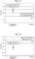
- Fig. 17 is a graph showing ratios N K1 /N K2 between the atom concentration N K1 (atm%) of potassium contained in the grain boundaries and the atom concentration N K2 (atm%) of potassium contained in the crystal grains of Example 1 and Comparative Example 1.
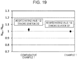
- Fig. 18 is a graph showing ratios N Na1 /N Na2 between the atom concentration N Na1 (atm%) of sodium contained in the grain boundaries and the atom concentration N Na2 (atm%) of sodium contained in the crystal grains of Example 1 and Comparative Example 1.
- Fig. 18 is a graph showing ratios N Na1 /N Na2 between the atom concentration N Na1 (atm%) of sodium contained in the grain boundaries and the atom concentration N Na2 (atm%) of sodium contained in the crystal grains of Example 1 and Comparative Example 1.
- Example 19 is a graph showing ratios N Nb1 /N Nb2 between the atom concentration N Nb1 (atm%) of niobium contained in the grain boundaries and the atom concentration N Nb2 (atm%) of niobium contained in the crystal grains of Example 1 and Comparative Example 1.
- the atom concentration ratios between atom concentration of atoms contained in the grain boundaries and atom concentration of atoms contained in the crystal grains were obtained as follows for potassium, sodium, and niobium.
- Fig. 20 is a graph showing distribution of potassium in Example 1.
- the distance (position) in which the intensity was the highest in the graph described above was set as a center of the grain boundary, and the intensity thereof was regarded as intensity corresponding to the atom concentration of potassium contained in the grain boundaries.
- the distance (position) in which the intensity was the lowest was set as a center of the grain boundary, and the intensity thereof was regarded as intensity corresponding to the atom concentration of sodium contained in the grain boundaries.
- Fig. 19 the distance (position) in which the intensity was the highest in the case of potassium was set as a center of a grain boundary, and average values of intensities in a range of ⁇ 30 nm from the center was regarded as intensities corresponding to atom concentrations of niobium contained in the grain boundaries. Further, uncertainty of the intensities corresponding to the atom concentrations of niobium contained in the grain boundaries was obtained. Then, similarly to Figs. 17 and 18 , intensities corresponding to the atom concentration of niobium contained in the crystal grains were obtained, and thus the atom concentration ratios were obtained.
- Fig. 21 is a graph showing distribution of potassium in Example 1 and Comparative Example 1. Fig. 21 is drawn on the basis of Fig. 20 .
- the distance (position) with the highest intensity was set as a center of a grain boundary.
- an intersection point P1 that is the closest to the center of the grain boundary among intersection points of a straight line L1 parallel to the horizontal axis and derived from an average value of a left region (region whose value on the horizontal axis is smaller than the center of the grain boundary) in a distance equal to or longer than 70 nm from the center of the grain boundary and a profile of intensity of Fig. 20 was obtained.
- an intersection point P2 that is the closest to the center of the grain boundary among intersection points of a straight line L2 parallel to the horizontal axis and derived from an average value of a right region (region whose value on the horizontal axis is larger than the center of the grain boundary) in a distance equal to or longer than 70 nm from the center of the grain boundary and the profile of intensity of Fig. 20 was obtained.
- An average value of a distance D1 between the intersection point P1 and the center of the grain boundary and a distance D2 between the intersection point P2 and the center of the grain boundary was obtained. The measurement described above was performed a plurality of times. In Fig. 21 , average values of measured values are shown as black dots, and variation (standard deviation) thereof is shown as error bars.
- Fig. 22 is a graph showing distribution of sodium in Example 1 and Comparative Example 1.
- Fig. 22 was generated in the same manner as Fig. 21 except that the distance (position) with the lowest intensity was regarded as a center of a grain boundary.
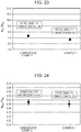
- Fig. 23 is a graph showing ratios N K3/ N K4 between the atom concentration N K3 (atm%) of potassium contained on the second electrode side of each of the crystal grain-containing layers and the atom concentration N K4 (atm%) of potassium contained on the first electrode side of each of the crystal grain-containing layers of Example 1 and Comparative Example 1.
- Fig. 24 is a graph showing ratios N Na3 /N Na4 between the atom concentration N Na3 (atm%) of sodium contained on the second electrode side of each of the crystal grain-containing layers and the atom concentration N Na4 (atm%) of sodium contained on the first electrode side of each of the crystal grain-containing layers of Example 1 and Comparative Example 1.
- Fig. 24 is a graph showing ratios N Na3 /N Na4 between the atom concentration N Na3 (atm%) of sodium contained on the second electrode side of each of the crystal grain-containing layers and the atom concentration N Na4 (atm%) of sodium contained on the first electrode side of each of the crystal grain-containing layers of Example 1 and Compar
- 25 is a graph showing ratios N Nb3 /N Nb4 between the atom concentration N Nb3 (atm%) of niobium contained on the second electrode side of each of the crystal grain-containing layers and the atom concentration N Nb4 (atm%) of niobium contained on the first electrode side of each of the crystal grain-containing layers of Example 1 and Comparative Example 1.
- the atom concentration ratios were obtained by respectively using the maximum value or the minimum value of the intensity of EDX on the first electrode side and the second electrode side.
- the maximum intensity on the second electrode side was regarded as the intensity corresponding to the atom concentration of atoms on the second electrode side
- the minimum intensity on the first electrode side was regarded as the intensity corresponding to the atom concentration of atoms on the first electrode side
- a ratio between these intensities was used as the atom concentration ratio.
- the measurement described above was performed a plurality of times.
- average values of the measured values are shown as black dots, and variation (standard deviation) thereof is shown as error bars.
- the invention includes configurations that are substantially the same as the configuration described in the embodiment (for example, configurations having the same functions, using the same methods, and having the same results, or configurations having the same object and the same effect).
- the invention includes configurations in which a portion that is not significant in the configuration described in the embodiment is replaced.
- the invention includes configurations that have the same effect as the configuration described in the embodiment and configurations that achieve the same object.
- the invention includes configurations in which a known technique is added to the configuration described in the embodiment.
Landscapes
- Engineering & Computer Science (AREA)
- Chemical & Material Sciences (AREA)
- Ceramic Engineering (AREA)
- Manufacturing & Machinery (AREA)
- Materials Engineering (AREA)
- Dispersion Chemistry (AREA)
- Structural Engineering (AREA)
- Organic Chemistry (AREA)
- Inorganic Chemistry (AREA)
- Particle Formation And Scattering Control In Inkjet Printers (AREA)
Claims (10)
- Élément piézoélectrique (100) comprenant :une première électrode (10) fournie au-dessus d'un substrat (2) ;une couche piézoélectrique (20) comprenant une pluralité de grains cristallins (24) contenant du potassium, du sodium et du niobium et fournie au-dessus de la première électrode ; etune deuxième électrode (30) fournie au-dessus de la couche piézoélectrique,caractérisé en cequ'une concentration atomique NK1 (atm%) de potassium contenu dans des joints de grains (26) des grains cristallins et une concentration atomique NK2 (atm%) de potassium contenu dans les grains cristallins satisfont à une relation de 1,0 < NK1/NK2 ≤ 2,4.
- Élément piézoélectrique selon la revendication 1, dans lequel une concentration atomique NNa1 (atm%) de sodium contenu dans les joints de grains est inférieure à une concentration atomique NNa2 (atm%) de sodium contenu dans les grains cristallins.
- Élément piézoélectrique selon la revendication 2, dans lequel la concentration atomique NNa1 et la concentration atomique NNa2 satisfont à la relation de 0,55 ≤ NNa1/NNa2 ≤ 0,75.
- Élément piézoélectrique selon l'une quelconque des revendications précédentes, dans lequel la concentration atomique NK1 et la concentration atomique NK2 satisfont à une relation de 1,5 ≤ NK1/NK2 ≤ 2, 0.
- Élément piézoélectrique selon l'une quelconque des revendications précédentes,
dans lequel la couche piézoélectrique comprend une pluralité de couches (22) contenant les grains cristallins laminées dans un sens de l'épaisseur de film, et
dans lequel une concentration atomique NK3 (atm%) de potassium sur le côté de deuxième électrode de chacune des couches contenant les grains cristallins est supérieure à une concentration atomique NK4 (atm%) de potassium du côté de la première électrode de chacune des couches contenant les grains cristallins. - Élément piézoélectrique selon la revendication 5, dans lequel la concentration atomique NK3 et la concentration atomique NK4 satisfont à une relation de 2, 0 ≤ NK3/NK4 ≤ 4,0.
- Élément piézoélectrique selon la revendication 5 ou la revendication 6, dans lequel une concentration atomique (atm%) de sodium contenu sur le côté de deuxième électrode de chacune des couches contenant les grains cristallins est inférieure à une concentration atomique (atm%) de sodium contenu sur le côté de première électrode de chacune des couches contenant les grains cristallins.
- Élément piézoélectrique selon l'une quelconque des revendications précédentes, dans lequel une concentration atomique (atm%) de potassium aux centres des joints de grains est supérieure à une concentration atomique (atm%) de potassium dans une zone à une distance supérieure ou égale à 70 nm par rapport aux centres des joints de grains.
- Élément piézoélectrique selon l'une quelconque des revendications précédentes, dans lequel une concentration atomique (atm%) de sodium aux centres des joints de grains est inférieure à une concentration atomique (atm%) de sodium dans une zone à une distance supérieure ou égale à 70 nm par rapport aux centres des joints de grains.
- Tête d'éjection de liquide (200) comprenant l'élément piézoélectrique selon l'une quelconque des revendications précédentes.
Applications Claiming Priority (1)
| Application Number | Priority Date | Filing Date | Title |
|---|---|---|---|
| JP2018033328A JP7087442B2 (ja) | 2018-02-27 | 2018-02-27 | 圧電素子および液体吐出ヘッド |
Publications (2)
| Publication Number | Publication Date |
|---|---|
| EP3531460A1 EP3531460A1 (fr) | 2019-08-28 |
| EP3531460B1 true EP3531460B1 (fr) | 2020-08-19 |
Family
ID=65576162
Family Applications (1)
| Application Number | Title | Priority Date | Filing Date |
|---|---|---|---|
| EP19158994.4A Active EP3531460B1 (fr) | 2018-02-27 | 2019-02-25 | Composant piézoélectrique et tête d'éjection de liquide |
Country Status (3)
| Country | Link |
|---|---|
| US (1) | US11309483B2 (fr) |
| EP (1) | EP3531460B1 (fr) |
| JP (1) | JP7087442B2 (fr) |
Families Citing this family (1)
| Publication number | Priority date | Publication date | Assignee | Title |
|---|---|---|---|---|
| JP2022011406A (ja) * | 2020-06-30 | 2022-01-17 | セイコーエプソン株式会社 | 圧電素子、液体吐出ヘッド、およびプリンター |
Family Cites Families (6)
| Publication number | Priority date | Publication date | Assignee | Title |
|---|---|---|---|---|
| JP3592053B2 (ja) | 1997-12-11 | 2004-11-24 | 株式会社リコー | インクジェットプリンタヘッド及びその製造方法 |
| JP4398635B2 (ja) * | 2002-09-24 | 2010-01-13 | 株式会社ノリタケカンパニーリミテド | 圧電セラミックス |
| JP4926389B2 (ja) | 2004-06-17 | 2012-05-09 | 株式会社豊田中央研究所 | 結晶配向セラミックス、及びその製造方法 |
| JP5662888B2 (ja) | 2011-07-04 | 2015-02-04 | 太陽誘電株式会社 | 多積層圧電セラミックス部品 |
| WO2013146975A1 (fr) | 2012-03-30 | 2013-10-03 | 日本碍子株式会社 | Élément de type de film piézoélectrique/électrorestrictif, et procédé de production d'élément de type de film piézoélectrique/électrorestrictif |
| US10355196B2 (en) | 2016-02-10 | 2019-07-16 | Seiko Epson Corporation | Piezoelectric element, piezoelectric element application device, and method of manufacturing piezoelectric element |
-
2018
- 2018-02-27 JP JP2018033328A patent/JP7087442B2/ja active Active
-
2019
- 2019-02-25 EP EP19158994.4A patent/EP3531460B1/fr active Active
- 2019-02-26 US US16/285,664 patent/US11309483B2/en active Active
Non-Patent Citations (1)
| Title |
|---|
| None * |
Also Published As
| Publication number | Publication date |
|---|---|
| JP2019149456A (ja) | 2019-09-05 |
| JP7087442B2 (ja) | 2022-06-21 |
| US20190267537A1 (en) | 2019-08-29 |
| US11309483B2 (en) | 2022-04-19 |
| EP3531460A1 (fr) | 2019-08-28 |
Similar Documents
| Publication | Publication Date | Title |
|---|---|---|
| US9356223B2 (en) | Liquid ejecting head and liquid ejecting apparatus | |
| EP3101703B1 (fr) | Élément piézoélectrique et tête imprimante à jet d'encre | |
| KR20160115768A (ko) | 압전 소자 및 압전 소자 응용 디바이스와 압전 소자의 제조 방법 | |
| JP2016082104A (ja) | 圧電素子及びその製造方法並びに圧電素子応用デバイス | |
| EP3382766B1 (fr) | Composant à couche piézoélectrique | |
| JP6652736B2 (ja) | 圧電素子、及び圧電素子応用デバイス | |
| JP6519735B2 (ja) | 圧電素子及び圧電素子応用デバイス | |
| EP3531460B1 (fr) | Composant piézoélectrique et tête d'éjection de liquide | |
| JP2016192511A (ja) | 圧電素子及び圧電素子応用デバイス | |
| US10734570B2 (en) | Piezoelectric element and piezoelectric element applied device | |
| JP6074130B2 (ja) | 圧電素子の製造方法、圧電素子、液体噴射ヘッド及び液体噴射装置 | |
| US9496485B2 (en) | Piezoelectric material, piezoelectric element, liquid ejecting head, liquid ejecting apparatus, and ultrasonic measuring apparatus | |
| JP7286929B2 (ja) | 圧電素子、液体吐出ヘッド、およびプリンター | |
| US20230354709A1 (en) | Method Of Manufacturing Piezoelectric Element | |
| US11535034B2 (en) | Piezoelectric element and liquid ejecting head including piezoelectric layer having improved lattice ratio | |
| US11014357B2 (en) | Piezoelectric element, liquid discharge head, and printer | |
| US20230320226A1 (en) | Piezoelectric Element And Piezoelectric Element Application Device | |
| JP2023114083A (ja) | 圧電素子、液滴吐出ヘッド、アクチュエーター、および振動子 | |
| JPH11157068A (ja) | 圧電体素子、インクジェット式記録ヘッドおよびそれらの製造方法 | |
| CN117835794A (zh) | 压电基板、压电元件以及压电元件应用器件 | |
| CN118632611A (zh) | 压电元件应用器件 | |
| JP2023096590A (ja) | 圧電体、圧電素子、および液体吐出ヘッド | |
| CN118076208A (zh) | 压电元件、压电致动器 | |
| JP2016157750A (ja) | 圧電素子及びその製造方法並びに圧電素子応用デバイス |
Legal Events
| Date | Code | Title | Description |
|---|---|---|---|
| PUAI | Public reference made under article 153(3) epc to a published international application that has entered the european phase |
Free format text: ORIGINAL CODE: 0009012 |
|
| STAA | Information on the status of an ep patent application or granted ep patent |
Free format text: STATUS: THE APPLICATION HAS BEEN PUBLISHED |
|
| AK | Designated contracting states |
Kind code of ref document: A1 Designated state(s): AL AT BE BG CH CY CZ DE DK EE ES FI FR GB GR HR HU IE IS IT LI LT LU LV MC MK MT NL NO PL PT RO RS SE SI SK SM TR |
|
| AX | Request for extension of the european patent |
Extension state: BA ME |
|
| STAA | Information on the status of an ep patent application or granted ep patent |
Free format text: STATUS: REQUEST FOR EXAMINATION WAS MADE |
|
| 17P | Request for examination filed |
Effective date: 20191021 |
|
| RBV | Designated contracting states (corrected) |
Designated state(s): AL AT BE BG CH CY CZ DE DK EE ES FI FR GB GR HR HU IE IS IT LI LT LU LV MC MK MT NL NO PL PT RO RS SE SI SK SM TR |
|
| GRAP | Despatch of communication of intention to grant a patent |
Free format text: ORIGINAL CODE: EPIDOSNIGR1 |
|
| STAA | Information on the status of an ep patent application or granted ep patent |
Free format text: STATUS: GRANT OF PATENT IS INTENDED |
|
| INTG | Intention to grant announced |
Effective date: 20200310 |
|
| GRAS | Grant fee paid |
Free format text: ORIGINAL CODE: EPIDOSNIGR3 |
|
| GRAA | (expected) grant |
Free format text: ORIGINAL CODE: 0009210 |
|
| STAA | Information on the status of an ep patent application or granted ep patent |
Free format text: STATUS: THE PATENT HAS BEEN GRANTED |
|
| AK | Designated contracting states |
Kind code of ref document: B1 Designated state(s): AL AT BE BG CH CY CZ DE DK EE ES FI FR GB GR HR HU IE IS IT LI LT LU LV MC MK MT NL NO PL PT RO RS SE SI SK SM TR |
|
| REG | Reference to a national code |
Ref country code: CH Ref legal event code: EP |
|
| REG | Reference to a national code |
Ref country code: DE Ref legal event code: R096 Ref document number: 602019000489 Country of ref document: DE |
|
| REG | Reference to a national code |
Ref country code: AT Ref legal event code: REF Ref document number: 1304950 Country of ref document: AT Kind code of ref document: T Effective date: 20200915 |
|
| REG | Reference to a national code |
Ref country code: IE Ref legal event code: FG4D |
|
| REG | Reference to a national code |
Ref country code: LT Ref legal event code: MG4D |
|
| REG | Reference to a national code |
Ref country code: NL Ref legal event code: MP Effective date: 20200819 |
|
| PG25 | Lapsed in a contracting state [announced via postgrant information from national office to epo] |
Ref country code: NO Free format text: LAPSE BECAUSE OF FAILURE TO SUBMIT A TRANSLATION OF THE DESCRIPTION OR TO PAY THE FEE WITHIN THE PRESCRIBED TIME-LIMIT Effective date: 20201119 Ref country code: BG Free format text: LAPSE BECAUSE OF FAILURE TO SUBMIT A TRANSLATION OF THE DESCRIPTION OR TO PAY THE FEE WITHIN THE PRESCRIBED TIME-LIMIT Effective date: 20201119 Ref country code: SE Free format text: LAPSE BECAUSE OF FAILURE TO SUBMIT A TRANSLATION OF THE DESCRIPTION OR TO PAY THE FEE WITHIN THE PRESCRIBED TIME-LIMIT Effective date: 20200819 Ref country code: LT Free format text: LAPSE BECAUSE OF FAILURE TO SUBMIT A TRANSLATION OF THE DESCRIPTION OR TO PAY THE FEE WITHIN THE PRESCRIBED TIME-LIMIT Effective date: 20200819 Ref country code: HR Free format text: LAPSE BECAUSE OF FAILURE TO SUBMIT A TRANSLATION OF THE DESCRIPTION OR TO PAY THE FEE WITHIN THE PRESCRIBED TIME-LIMIT Effective date: 20200819 Ref country code: GR Free format text: LAPSE BECAUSE OF FAILURE TO SUBMIT A TRANSLATION OF THE DESCRIPTION OR TO PAY THE FEE WITHIN THE PRESCRIBED TIME-LIMIT Effective date: 20201120 Ref country code: FI Free format text: LAPSE BECAUSE OF FAILURE TO SUBMIT A TRANSLATION OF THE DESCRIPTION OR TO PAY THE FEE WITHIN THE PRESCRIBED TIME-LIMIT Effective date: 20200819 Ref country code: PT Free format text: LAPSE BECAUSE OF FAILURE TO SUBMIT A TRANSLATION OF THE DESCRIPTION OR TO PAY THE FEE WITHIN THE PRESCRIBED TIME-LIMIT Effective date: 20201221 |
|
| REG | Reference to a national code |
Ref country code: AT Ref legal event code: MK05 Ref document number: 1304950 Country of ref document: AT Kind code of ref document: T Effective date: 20200819 |
|
| PG25 | Lapsed in a contracting state [announced via postgrant information from national office to epo] |
Ref country code: LV Free format text: LAPSE BECAUSE OF FAILURE TO SUBMIT A TRANSLATION OF THE DESCRIPTION OR TO PAY THE FEE WITHIN THE PRESCRIBED TIME-LIMIT Effective date: 20200819 Ref country code: NL Free format text: LAPSE BECAUSE OF FAILURE TO SUBMIT A TRANSLATION OF THE DESCRIPTION OR TO PAY THE FEE WITHIN THE PRESCRIBED TIME-LIMIT Effective date: 20200819 Ref country code: RS Free format text: LAPSE BECAUSE OF FAILURE TO SUBMIT A TRANSLATION OF THE DESCRIPTION OR TO PAY THE FEE WITHIN THE PRESCRIBED TIME-LIMIT Effective date: 20200819 Ref country code: PL Free format text: LAPSE BECAUSE OF FAILURE TO SUBMIT A TRANSLATION OF THE DESCRIPTION OR TO PAY THE FEE WITHIN THE PRESCRIBED TIME-LIMIT Effective date: 20200819 Ref country code: IS Free format text: LAPSE BECAUSE OF FAILURE TO SUBMIT A TRANSLATION OF THE DESCRIPTION OR TO PAY THE FEE WITHIN THE PRESCRIBED TIME-LIMIT Effective date: 20201219 |
|
| PG25 | Lapsed in a contracting state [announced via postgrant information from national office to epo] |
Ref country code: SM Free format text: LAPSE BECAUSE OF FAILURE TO SUBMIT A TRANSLATION OF THE DESCRIPTION OR TO PAY THE FEE WITHIN THE PRESCRIBED TIME-LIMIT Effective date: 20200819 Ref country code: RO Free format text: LAPSE BECAUSE OF FAILURE TO SUBMIT A TRANSLATION OF THE DESCRIPTION OR TO PAY THE FEE WITHIN THE PRESCRIBED TIME-LIMIT Effective date: 20200819 Ref country code: CZ Free format text: LAPSE BECAUSE OF FAILURE TO SUBMIT A TRANSLATION OF THE DESCRIPTION OR TO PAY THE FEE WITHIN THE PRESCRIBED TIME-LIMIT Effective date: 20200819 Ref country code: DK Free format text: LAPSE BECAUSE OF FAILURE TO SUBMIT A TRANSLATION OF THE DESCRIPTION OR TO PAY THE FEE WITHIN THE PRESCRIBED TIME-LIMIT Effective date: 20200819 Ref country code: EE Free format text: LAPSE BECAUSE OF FAILURE TO SUBMIT A TRANSLATION OF THE DESCRIPTION OR TO PAY THE FEE WITHIN THE PRESCRIBED TIME-LIMIT Effective date: 20200819 |
|
| REG | Reference to a national code |
Ref country code: DE Ref legal event code: R097 Ref document number: 602019000489 Country of ref document: DE |
|
| PG25 | Lapsed in a contracting state [announced via postgrant information from national office to epo] |
Ref country code: AL Free format text: LAPSE BECAUSE OF FAILURE TO SUBMIT A TRANSLATION OF THE DESCRIPTION OR TO PAY THE FEE WITHIN THE PRESCRIBED TIME-LIMIT Effective date: 20200819 Ref country code: AT Free format text: LAPSE BECAUSE OF FAILURE TO SUBMIT A TRANSLATION OF THE DESCRIPTION OR TO PAY THE FEE WITHIN THE PRESCRIBED TIME-LIMIT Effective date: 20200819 Ref country code: ES Free format text: LAPSE BECAUSE OF FAILURE TO SUBMIT A TRANSLATION OF THE DESCRIPTION OR TO PAY THE FEE WITHIN THE PRESCRIBED TIME-LIMIT Effective date: 20200819 |
|
| PLBE | No opposition filed within time limit |
Free format text: ORIGINAL CODE: 0009261 |
|
| STAA | Information on the status of an ep patent application or granted ep patent |
Free format text: STATUS: NO OPPOSITION FILED WITHIN TIME LIMIT |
|
| PG25 | Lapsed in a contracting state [announced via postgrant information from national office to epo] |
Ref country code: SK Free format text: LAPSE BECAUSE OF FAILURE TO SUBMIT A TRANSLATION OF THE DESCRIPTION OR TO PAY THE FEE WITHIN THE PRESCRIBED TIME-LIMIT Effective date: 20200819 |
|
| 26N | No opposition filed |
Effective date: 20210520 |
|
| PG25 | Lapsed in a contracting state [announced via postgrant information from national office to epo] |
Ref country code: IT Free format text: LAPSE BECAUSE OF FAILURE TO SUBMIT A TRANSLATION OF THE DESCRIPTION OR TO PAY THE FEE WITHIN THE PRESCRIBED TIME-LIMIT Effective date: 20200819 |
|
| PG25 | Lapsed in a contracting state [announced via postgrant information from national office to epo] |
Ref country code: SI Free format text: LAPSE BECAUSE OF FAILURE TO SUBMIT A TRANSLATION OF THE DESCRIPTION OR TO PAY THE FEE WITHIN THE PRESCRIBED TIME-LIMIT Effective date: 20200819 |
|
| PG25 | Lapsed in a contracting state [announced via postgrant information from national office to epo] |
Ref country code: MC Free format text: LAPSE BECAUSE OF FAILURE TO SUBMIT A TRANSLATION OF THE DESCRIPTION OR TO PAY THE FEE WITHIN THE PRESCRIBED TIME-LIMIT Effective date: 20200819 |
|
| REG | Reference to a national code |
Ref country code: BE Ref legal event code: MM Effective date: 20210228 |
|
| PG25 | Lapsed in a contracting state [announced via postgrant information from national office to epo] |
Ref country code: LU Free format text: LAPSE BECAUSE OF NON-PAYMENT OF DUE FEES Effective date: 20210225 |
|
| PG25 | Lapsed in a contracting state [announced via postgrant information from national office to epo] |
Ref country code: FR Free format text: LAPSE BECAUSE OF NON-PAYMENT OF DUE FEES Effective date: 20210228 Ref country code: IE Free format text: LAPSE BECAUSE OF NON-PAYMENT OF DUE FEES Effective date: 20210225 |
|
| PG25 | Lapsed in a contracting state [announced via postgrant information from national office to epo] |
Ref country code: BE Free format text: LAPSE BECAUSE OF NON-PAYMENT OF DUE FEES Effective date: 20210228 |
|
| REG | Reference to a national code |
Ref country code: CH Ref legal event code: PL |
|
| REG | Reference to a national code |
Ref country code: DE Ref legal event code: R079 Ref document number: 602019000489 Country of ref document: DE Free format text: PREVIOUS MAIN CLASS: H01L0041187000 Ipc: H10N0030853000 |
|
| PG25 | Lapsed in a contracting state [announced via postgrant information from national office to epo] |
Ref country code: LI Free format text: LAPSE BECAUSE OF NON-PAYMENT OF DUE FEES Effective date: 20220228 Ref country code: CH Free format text: LAPSE BECAUSE OF NON-PAYMENT OF DUE FEES Effective date: 20220228 |
|
| PG25 | Lapsed in a contracting state [announced via postgrant information from national office to epo] |
Ref country code: CY Free format text: LAPSE BECAUSE OF FAILURE TO SUBMIT A TRANSLATION OF THE DESCRIPTION OR TO PAY THE FEE WITHIN THE PRESCRIBED TIME-LIMIT Effective date: 20200819 |
|
| PG25 | Lapsed in a contracting state [announced via postgrant information from national office to epo] |
Ref country code: HU Free format text: LAPSE BECAUSE OF FAILURE TO SUBMIT A TRANSLATION OF THE DESCRIPTION OR TO PAY THE FEE WITHIN THE PRESCRIBED TIME-LIMIT; INVALID AB INITIO Effective date: 20190225 |
|
| GBPC | Gb: european patent ceased through non-payment of renewal fee |
Effective date: 20230225 |
|
| PG25 | Lapsed in a contracting state [announced via postgrant information from national office to epo] |
Ref country code: GB Free format text: LAPSE BECAUSE OF NON-PAYMENT OF DUE FEES Effective date: 20230225 |
|
| PG25 | Lapsed in a contracting state [announced via postgrant information from national office to epo] |
Ref country code: GB Free format text: LAPSE BECAUSE OF NON-PAYMENT OF DUE FEES Effective date: 20230225 |
|
| PG25 | Lapsed in a contracting state [announced via postgrant information from national office to epo] |
Ref country code: MK Free format text: LAPSE BECAUSE OF FAILURE TO SUBMIT A TRANSLATION OF THE DESCRIPTION OR TO PAY THE FEE WITHIN THE PRESCRIBED TIME-LIMIT Effective date: 20200819 |
|
| PGFP | Annual fee paid to national office [announced via postgrant information from national office to epo] |
Ref country code: DE Payment date: 20231229 Year of fee payment: 6 |
|
| PG25 | Lapsed in a contracting state [announced via postgrant information from national office to epo] |
Ref country code: TR Free format text: LAPSE BECAUSE OF FAILURE TO SUBMIT A TRANSLATION OF THE DESCRIPTION OR TO PAY THE FEE WITHIN THE PRESCRIBED TIME-LIMIT Effective date: 20200819 |