EP3522353B1 - Umrichtervorrichtung - Google Patents
Umrichtervorrichtung Download PDFInfo
- Publication number
- EP3522353B1 EP3522353B1 EP17855301.2A EP17855301A EP3522353B1 EP 3522353 B1 EP3522353 B1 EP 3522353B1 EP 17855301 A EP17855301 A EP 17855301A EP 3522353 B1 EP3522353 B1 EP 3522353B1
- Authority
- EP
- European Patent Office
- Prior art keywords
- voltage
- phase
- ripple component
- frequency
- axis
- Prior art date
- Legal status (The legal status is an assumption and is not a legal conclusion. Google has not performed a legal analysis and makes no representation as to the accuracy of the status listed.)
- Active
Links
Images




Classifications
-
- H—ELECTRICITY
- H02—GENERATION; CONVERSION OR DISTRIBUTION OF ELECTRIC POWER
- H02M—APPARATUS FOR CONVERSION BETWEEN AC AND AC, BETWEEN AC AND DC, OR BETWEEN DC AND DC, AND FOR USE WITH MAINS OR SIMILAR POWER SUPPLY SYSTEMS; CONVERSION OF DC OR AC INPUT POWER INTO SURGE OUTPUT POWER; CONTROL OR REGULATION THEREOF
- H02M5/00—Conversion of AC power input into AC power output, e.g. for change of voltage, for change of frequency, for change of number of phases
- H02M5/40—Conversion of AC power input into AC power output, e.g. for change of voltage, for change of frequency, for change of number of phases with intermediate conversion into DC
- H02M5/42—Conversion of AC power input into AC power output, e.g. for change of voltage, for change of frequency, for change of number of phases with intermediate conversion into DC by static converters
- H02M5/44—Conversion of AC power input into AC power output, e.g. for change of voltage, for change of frequency, for change of number of phases with intermediate conversion into DC by static converters using discharge tubes or semiconductor devices to convert the intermediate DC into AC
- H02M5/453—Conversion of AC power input into AC power output, e.g. for change of voltage, for change of frequency, for change of number of phases with intermediate conversion into DC by static converters using discharge tubes or semiconductor devices to convert the intermediate DC into AC using devices of a triode or transistor type requiring continuous application of a control signal
- H02M5/458—Conversion of AC power input into AC power output, e.g. for change of voltage, for change of frequency, for change of number of phases with intermediate conversion into DC by static converters using discharge tubes or semiconductor devices to convert the intermediate DC into AC using devices of a triode or transistor type requiring continuous application of a control signal using semiconductor devices only
-
- H—ELECTRICITY
- H02—GENERATION; CONVERSION OR DISTRIBUTION OF ELECTRIC POWER
- H02P—CONTROL OR REGULATION OF ELECTRIC MOTORS, ELECTRIC GENERATORS OR DYNAMO-ELECTRIC CONVERTERS; CONTROLLING TRANSFORMERS, REACTORS OR CHOKE COILS
- H02P21/00—Arrangements or methods for the control of electric machines by vector control, e.g. by control of field orientation
- H02P21/05—Arrangements or methods for the control of electric machines by vector control, e.g. by control of field orientation specially adapted for damping motor oscillations, e.g. for reducing hunting
-
- H—ELECTRICITY
- H02—GENERATION; CONVERSION OR DISTRIBUTION OF ELECTRIC POWER
- H02M—APPARATUS FOR CONVERSION BETWEEN AC AND AC, BETWEEN AC AND DC, OR BETWEEN DC AND DC, AND FOR USE WITH MAINS OR SIMILAR POWER SUPPLY SYSTEMS; CONVERSION OF DC OR AC INPUT POWER INTO SURGE OUTPUT POWER; CONTROL OR REGULATION THEREOF
- H02M1/00—Details of apparatus for conversion
- H02M1/12—Arrangements for reducing harmonics from AC input or output
- H02M1/126—Arrangements for reducing harmonics from AC input or output using passive filters
-
- H—ELECTRICITY
- H02—GENERATION; CONVERSION OR DISTRIBUTION OF ELECTRIC POWER
- H02M—APPARATUS FOR CONVERSION BETWEEN AC AND AC, BETWEEN AC AND DC, OR BETWEEN DC AND DC, AND FOR USE WITH MAINS OR SIMILAR POWER SUPPLY SYSTEMS; CONVERSION OF DC OR AC INPUT POWER INTO SURGE OUTPUT POWER; CONTROL OR REGULATION THEREOF
- H02M1/00—Details of apparatus for conversion
- H02M1/14—Arrangements for reducing ripples from DC input or output
-
- H—ELECTRICITY
- H02—GENERATION; CONVERSION OR DISTRIBUTION OF ELECTRIC POWER
- H02M—APPARATUS FOR CONVERSION BETWEEN AC AND AC, BETWEEN AC AND DC, OR BETWEEN DC AND DC, AND FOR USE WITH MAINS OR SIMILAR POWER SUPPLY SYSTEMS; CONVERSION OF DC OR AC INPUT POWER INTO SURGE OUTPUT POWER; CONTROL OR REGULATION THEREOF
- H02M7/00—Conversion of AC power input into DC power output; Conversion of DC power input into AC power output
- H02M7/02—Conversion of AC power input into DC power output without possibility of reversal
- H02M7/04—Conversion of AC power input into DC power output without possibility of reversal by static converters
- H02M7/06—Conversion of AC power input into DC power output without possibility of reversal by static converters using discharge tubes without control electrode or semiconductor devices without control electrode
-
- H—ELECTRICITY
- H02—GENERATION; CONVERSION OR DISTRIBUTION OF ELECTRIC POWER
- H02M—APPARATUS FOR CONVERSION BETWEEN AC AND AC, BETWEEN AC AND DC, OR BETWEEN DC AND DC, AND FOR USE WITH MAINS OR SIMILAR POWER SUPPLY SYSTEMS; CONVERSION OF DC OR AC INPUT POWER INTO SURGE OUTPUT POWER; CONTROL OR REGULATION THEREOF
- H02M7/00—Conversion of AC power input into DC power output; Conversion of DC power input into AC power output
- H02M7/42—Conversion of DC power input into AC power output without possibility of reversal
- H02M7/44—Conversion of DC power input into AC power output without possibility of reversal by static converters
- H02M7/48—Conversion of DC power input into AC power output without possibility of reversal by static converters using discharge tubes with control electrode or semiconductor devices with control electrode
-
- H—ELECTRICITY
- H02—GENERATION; CONVERSION OR DISTRIBUTION OF ELECTRIC POWER
- H02M—APPARATUS FOR CONVERSION BETWEEN AC AND AC, BETWEEN AC AND DC, OR BETWEEN DC AND DC, AND FOR USE WITH MAINS OR SIMILAR POWER SUPPLY SYSTEMS; CONVERSION OF DC OR AC INPUT POWER INTO SURGE OUTPUT POWER; CONTROL OR REGULATION THEREOF
- H02M7/00—Conversion of AC power input into DC power output; Conversion of DC power input into AC power output
- H02M7/42—Conversion of DC power input into AC power output without possibility of reversal
- H02M7/44—Conversion of DC power input into AC power output without possibility of reversal by static converters
- H02M7/48—Conversion of DC power input into AC power output without possibility of reversal by static converters using discharge tubes with control electrode or semiconductor devices with control electrode
- H02M7/53—Conversion of DC power input into AC power output without possibility of reversal by static converters using discharge tubes with control electrode or semiconductor devices with control electrode using devices of a triode or transistor type requiring continuous application of a control signal
- H02M7/537—Conversion of DC power input into AC power output without possibility of reversal by static converters using discharge tubes with control electrode or semiconductor devices with control electrode using devices of a triode or transistor type requiring continuous application of a control signal using semiconductor devices only, e.g. single switched pulse inverters
- H02M7/5387—Conversion of DC power input into AC power output without possibility of reversal by static converters using discharge tubes with control electrode or semiconductor devices with control electrode using devices of a triode or transistor type requiring continuous application of a control signal using semiconductor devices only, e.g. single switched pulse inverters in a bridge configuration
-
- H—ELECTRICITY
- H02—GENERATION; CONVERSION OR DISTRIBUTION OF ELECTRIC POWER
- H02P—CONTROL OR REGULATION OF ELECTRIC MOTORS, ELECTRIC GENERATORS OR DYNAMO-ELECTRIC CONVERTERS; CONTROLLING TRANSFORMERS, REACTORS OR CHOKE COILS
- H02P21/00—Arrangements or methods for the control of electric machines by vector control, e.g. by control of field orientation
-
- H—ELECTRICITY
- H02—GENERATION; CONVERSION OR DISTRIBUTION OF ELECTRIC POWER
- H02P—CONTROL OR REGULATION OF ELECTRIC MOTORS, ELECTRIC GENERATORS OR DYNAMO-ELECTRIC CONVERTERS; CONTROLLING TRANSFORMERS, REACTORS OR CHOKE COILS
- H02P21/00—Arrangements or methods for the control of electric machines by vector control, e.g. by control of field orientation
- H02P21/22—Current control, e.g. using a current control loop
-
- H—ELECTRICITY
- H02—GENERATION; CONVERSION OR DISTRIBUTION OF ELECTRIC POWER
- H02P—CONTROL OR REGULATION OF ELECTRIC MOTORS, ELECTRIC GENERATORS OR DYNAMO-ELECTRIC CONVERTERS; CONTROLLING TRANSFORMERS, REACTORS OR CHOKE COILS
- H02P27/00—Arrangements or methods for the control of AC motors characterised by the kind of supply voltage
- H02P27/04—Arrangements or methods for the control of AC motors characterised by the kind of supply voltage using variable-frequency supply voltage, e.g. inverter or converter supply voltage
-
- H—ELECTRICITY
- H02—GENERATION; CONVERSION OR DISTRIBUTION OF ELECTRIC POWER
- H02P—CONTROL OR REGULATION OF ELECTRIC MOTORS, ELECTRIC GENERATORS OR DYNAMO-ELECTRIC CONVERTERS; CONTROLLING TRANSFORMERS, REACTORS OR CHOKE COILS
- H02P29/00—Arrangements for regulating or controlling electric motors, appropriate for both AC and DC motors
- H02P29/50—Reduction of harmonics
-
- H—ELECTRICITY
- H02—GENERATION; CONVERSION OR DISTRIBUTION OF ELECTRIC POWER
- H02M—APPARATUS FOR CONVERSION BETWEEN AC AND AC, BETWEEN AC AND DC, OR BETWEEN DC AND DC, AND FOR USE WITH MAINS OR SIMILAR POWER SUPPLY SYSTEMS; CONVERSION OF DC OR AC INPUT POWER INTO SURGE OUTPUT POWER; CONTROL OR REGULATION THEREOF
- H02M1/00—Details of apparatus for conversion
- H02M1/0003—Details of control, feedback or regulation circuits
- H02M1/0016—Control circuits providing compensation of output voltage deviations using feedforward of disturbance parameters
- H02M1/0022—Control circuits providing compensation of output voltage deviations using feedforward of disturbance parameters the disturbance parameters being input voltage fluctuations
Definitions
- the present invention relates to an inverter device.
- a general three-phase inverter device smooths out voltage ripple occurring in a diode bridge by providing a capacitor and a reactor in a smoothing circuit.
- a large capacitor and a large reactor are required to smooth out voltage ripple, which raises a problem of increase in cost and volume.
- the largest frequency component generated in the DC link voltage is six times the power source frequency (300 Hz at 50 Hz, 360 Hz at 60 Hz), and when the number of motor pole pairs is three, the beat phenomenon becomes most prominent around 100 rps (300 Hz) or 120 rps (360 Hz).
- Such a beat phenomenon causes problems such as increase in the rms value and peak current, and vibration of the motor. Hence, a technique for suppressing beat is necessary.
- a conventional inverter device detects ripple in a DC link voltage and corrects the voltage, so that a voltage according to a voltage command is applied from the inverter device to a motor to suppress beat (for example, refer to JP S61-48356 A (Patent Literature 1)). As a result, ripple in the voltage applied to the motor is suppressed, and ripple and beat in the motor current are suppressed.
- the patent application publication US2014232309A1 discloses a space vector controlled inverter device comprising a three-phase rectifier, a DC link circuit, a three-phase inverter, and an inverter control device.
- Patent Literature 1 JP S61-48356 A
- the modulation factor is corrected so as to eliminate ripple in the voltage applied to the motor, the voltage can only be utilized by 86.6% (see FIG. 4 ) of the maximum value of the DC link voltage. Accordingly, the voltage utilization factor decreases and the motor current rms value increases.
- the modulation factor is set to the maximum possible modulation factor.
- the voltage utilization factor increases, the motor output voltage pulsates, and therefore problems such as ripple and beat in the motor current occur.
- the modulation factor is set to the maximum possible modulation factor, whereby the voltage applied to the motor pulsates according to the DC voltage.
- ripple and beat occur in the motor current according to the voltage ripple of the motor.
- an inverter device of the invention includes:
- the control device controls the inverter section so that the phase of the d-axis voltage Vd of the ripple component included in the DC voltage from the converter section leads the phase of the q-axis voltage Vq, whereby it is possible to control the phase of the output voltage to the motor according to ripple in the output voltage to the motor without lowering voltage utilization factor, and it is possible to suppress ripple and beat in the motor current.
- control device (100) controls the inverter section so that the phase of the d-axis voltage Vd of the ripple component included in the DC voltage leads the phase of the q-axis voltage Vq by 90 degrees in the rotating coordinate.
- control device controlls the inverter section so that the phase of the d-axis voltage Vd of the ripple component included in the DC voltage from the converter section leads the phase of the q-axis voltage Vq by 90 degrees in the rotating coordinate, whereby it is possible to effectively suppress ripple and beat in the motor current.
- control device includes:
- the phase of the ripple component included in the DC voltage is determined by the ripple component phase determination unit based on the phase of the three-phase AC voltage detected by the phase detector. Hence, it is possible to detect the phase of the ripple component with a simple configuration. Based on the determined phase of the ripple component included in the DC voltage, the output voltage phase correction unit corrects the phase of the output voltage output from the inverter section so that the phase of the d-axis voltage Vd of the ripple component included in the DC voltage leads the phase of the q-axis voltage Vq by 90 degrees. Hence, it is possible to reliably suppress ripple and beat in the motor current.
- control device controls the inverter section so that a locus of a voltage vector on the d and q axes of the rotating coordinate of an output voltage output from the inverter section (22) becomes circular.
- the output voltage phase correction unit includes:
- the inverter device of one embodiment also includes an LC filter that has a reactor connected to one of two output ends of the converter section and one of two input ends of the inverter section, and a capacitor connected between the input ends of the inverter section.
- a characteristic of the LC filter is set so that a resonance frequency of the LC filter is a frequency equal to or more than six times a commercial frequency of the three-phase AC voltage input into the converter section, and is a frequency that attenuates a current having the same frequency as a carrier frequency of the inverter section.
- a large capacitor and a large reactor for smoothing need not be provided in a DC link portion, whereby cost and size can be reduced.
- the invention can implement an inverter device capable of reducing ripple in a motor current when a DC link voltage pulsates due to the power source frequency.
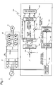
- FIG. 1 is a configuration diagram of an inverter device of a first embodiment of the invention.
- the inverter device of the first embodiment includes a converter section 21 including six diodes D11 to D16 that form a three-phase diode bridge circuit, an inverter section 22 including six switching elements S11 to S16 that form a three-phase bridge circuit, and a control device 100 that controls the inverter section 22.
- the inverter device also includes an inductor Ldc connected between a positive output end of the converter section 21 and a positive input end of the inverter section 22, and a capacitor Cdc connected between the input ends of the inverter section 22.
- the inductor Ldc and the capacitor Cdc form an LC filter.
- the converter section 21 rectifies a three-phase AC voltage from a three-phase AC power source 10 into DC
- the inverter section 22 converts the rectified DC voltage into a desired three-phase AC voltage to output the three-phase AC voltage to a motor 23.
- the control device 100 includes: a zero-crossing detector 101 that detects zero-crossing of a line voltage of the three-phase AC voltage; a Vdc ripple component phase detector 102 that outputs a signal indicating a phase ⁇ Vdc of a Vdc ripple component based on a zero-crossing signal; a compensation signal generator 103 that outputs a compensation signal ⁇ h based on the signal indicating the phase ⁇ Vdc of the Vdc ripple component from the Vdc ripple component phase detector 102; an adder-subtractor 104 that subtracts an actual speed ⁇ from a speed command ⁇ *; a motor control unit 105 that outputs voltage commands v d *, v q * based on a signal from the adder-subtractor 104; a polar coordinate converter 106 that converts the voltage commands v d *, v q * from the motor control unit 105 into polar coordinates; an adder-subtractor 107 that adds a voltage phase command ⁇
- the zero-crossing detector 101 outputs a zero-crossing signal indicating zero-crossing of an AC waveform based on the line voltage of the three-phase AC voltage from the three-phase AC power source 10.
- the zero-crossing detector 101 is an example of a phase detector.
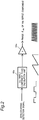
- the Vdc ripple component phase detector 102 includes: a Vdc ripple component phase calculation unit 102a that outputs a triangular wave synchronized with the zero-crossing signal (rectangular wave) from the zero-crossing detector 101 based on the zero-crossing signal; and a multiplier 102b that multiplies a signal indicating the Vdc ripple component from the Vdc ripple component phase calculation unit 102a by 6 and outputs a signal indicating the phase ⁇ Vdc of the Vdc ripple component.
- the Vdc ripple component phase detector 102 is an example of a ripple component phase determination unit.
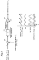
- the compensation signal generator 103 includes: an adder-subtractor 103a that adds the signal indicating the phase ⁇ Vdc of the Vdc ripple component from the Vdc ripple component phase detector 102 and a phase correction amount k ⁇ (fixed value); a phase-to-sinusoidal wave converter 103b that converts the signal, to which the phase correction amount k ⁇ is added by the adder-subtractor 103a, into a sine wave; and a multiplication device 103c that corrects the gain of the compensation signal from the phase-to-sinusoidal wave converter 103b and outputs a compensation signal ⁇ h .
- a gain correction amount k a of the multiplication device 103c is a fixed value.
- the compensation signal generator 103 is an example of an output voltage phase correction unit.
- FIG. 3 The lower side of FIG. 3 is a diagram of a waveform of the phase ⁇ Vdc of the Vdc ripple component, a Vdc waveform, a waveform of Vdc ripple, and a waveform of the compensation signal ⁇ h .
- the characteristics of the LC filter are set so that the resonance frequency of the LC filter may be a frequency equal to or more than six times the commercial frequency of the three-phase AC voltage input into the converter section 21, and may be a frequency that attenuates a current having the same frequency as the carrier frequency of the inverter section 22. That is, the LC filter has no effect of smoothing the commercial frequency component.
- Equation (2) Ignoring the steady-state term ⁇ er ⁇ a (voltage induced by magnetic flux of magnet) and transforming Equation (1) as a frequency transfer function, following Equation (2) is obtained.
- FIG. 10 is a diagram of the relationship between the Vq ripple and the Vd ripple with respect to the Vdc ripple, and ⁇ p indicates the phase difference between the Vd ripple and the Vq ripple.
- ⁇ p 90 degrees (Vd leads Vq by 90 degrees) is illustrated.
- Vd and Vq are defined as a constant phase as illustrated in following Equation (3).
- V d j ⁇ V q j ⁇ V amp j ⁇ ⁇ sin ⁇ cos ⁇
- Equation (3) is a function related to ⁇ er as illustrated in following Equation (4).
- Ia is minimized by minimizing the ripple component of each of Id and Iq.
- I d I q 1 G R a + j ⁇ dc L q ⁇ er L q ⁇ ⁇ er L d R a + V d v q and focusing only on the numerator of Equation (5) and replacing ⁇ dc with ⁇ er , the following equation is obtained.
- I d I q R a V d + ⁇ er L q jV d + V q R a V q ⁇ ⁇ er L d V d ⁇ jV q
- the vector diagram is as illustrated in FIG. 11A , and the amplitude of the vector is the sum of both vectors.
- I d I q R a V d R a V q
- FIG. 5 is a diagram of waveforms of a zero-crossing detection signal, a DC link voltage, a ripple component of the DC link voltage, and a compensation signal.
- Vd leads Vq by 90 degrees. Accordingly, the phase should be compensated so as to draw a counterclockwise circular locus as illustrated in the vector diagram of FIG. 6 .
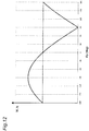
- r is the average value V dc_ave of the output voltage
- phase ⁇ V dc _ max ⁇ V dc _ a ⁇ e V dc _ a ⁇ e
- the control device 100 controls the inverter section 22 so that the the phase of d-axis voltage Vd of the ripple component included in the DC voltage from the converter section 21 leads the phase of the q-axis voltage Vq by 90 degrees, whereby it is possible to control the phase of the output voltage to the motor 23 according to ripple in the output voltage to the motor 23 without lowering voltage utilization factor, and it is possible to suppress ripple and beat in the motor current.
- the Vdc ripple component phase detector 102 determines the phase of the ripple component included in the DC voltage. Hence, it is possible to detect the phase of the ripple component with a simple configuration.
- the compensation signal generator 103 output voltage phase correction unit
- the compensation signal generator 103 corrects the phase of the output voltage output from the inverter section so that the phase of the d-axis voltage Vd of the ripple component included in the DC voltage leads the phase of the q-axis voltage Vq by 90 degrees. Hence, it is possible to reliably suppress ripple and beat in the motor current.
- the characteristics of the LC filter are set so that the resonance frequency of the LC filter formed of the inductor Ldc and the capacitor Cdc is a frequency equal to or more than six times the commercial frequency of the three-phase AC voltage input into the converter section 21, and is a frequency that attenuates a current having the same frequency as the carrier frequency of the inverter section 22.
- a large capacitor and a large reactor for smoothing need not be provided in the DC link portion, whereby cost and size can be reduced.
- the first embodiment describes the inverter device that compensates for the ripple component that is six times the power source frequency.
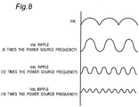
- a DC link voltage actually includes harmonics that are multiples of the ripple component that is six times the power source frequency.
- the second embodiment of the invention describes an inverter device capable of suppressing, by a similar method, the influence of power ripple caused by such harmonics.
- current ripple can be suppressed by generating current ripple as in the case of the ripple having the frequency of six times the power source frequency, and injecting a compensation signal with the same principle.
- FIG. 9 is a configuration diagram of a compensation signal generator 210 of the inverter device of the second embodiment. Note that the inverter device of the second embodiment has the same configuration as that of the inverter device of the first embodiment except for the compensation signal generator 210, and therefore cites FIG. 1 .
- the compensation signal generator 210 includes: an adder-subtractor 201-1 that adds a signal indicating a phase ⁇ Vdc of a Vdc ripple component from the Vdc ripple component phase detector 102 (illustrated in FIG. 1 ) and a phase correction amount k ⁇ 1 ; a phase-to-sinusoidal wave converter 202-1 that converts the signal, to which the phase correction amount k ⁇ 1 is added by the adder-subtractor 201-1, into a sine wave; and a multiplication device 203-1 that corrects the gain of the compensation signal from the phase-to-sinusoidal wave converter 202-1 and outputs a compensation signal ⁇ h1 .
- the adder-subtractor 201-1, the phase-to-sinusoidal wave converter 202-1, and the multiplication device 203-1 form a first output voltage phase correction unit.
- the compensation signal generator 210 also includes: multipliers 200-2, 200-3, ..., 200-N that respectively multiply signals indicating the phase ⁇ Vdc of the Vdc ripple component from the Vdc ripple component phase detector 102 by 2, 3, ..., N; adder-subtractors 201-2, 201-3, ..., 201-N that respectively add the signals from the multipliers 200-2, 200-3, ..., 200-N and phase correction amounts k ⁇ 2 , k ⁇ 3 , ..., k ⁇ N ; phase-to-sinusoidal wave converters 202-2, 202-3, ..., 202-N that respectively convert the signals, to which the phase correction amounts k ⁇ 2 , k ⁇ 3 , ..., k ⁇ N are added by the adder-subtractors 201-2, 201-3, ..., 201-N, into sine waves; and multiplication devices 203-2, 203-3, ..., 203-N that correct respective gains of the compensation signals from the phase-to-sinusoidal wave converters
- gain correction amounts k 1 , k 2 , k 3 , ..., k N of the multiplication devices 203-1, 203-2, 203-3, ..., 203-N are fixed values.
- the multipliers 200-2, 200-3, ..., 200-N, the adder-subtractors 201-2, 201-3, ..., 201-N, the phase-to-sinusoidal wave converters 202-2, 202-3, ..., 202-N, and the multiplication devices 203-2, 203-3, ..., 203-N form second to Nth output voltage phase correction units.
- the compensation signal generator 210 also includes an adder-subtractor 204 that adds the compensation signals ⁇ h1 , ⁇ h2 , ⁇ h3 , ..., ⁇ hN from the multiplication devices 203-1, 203-2, 203-3, ..., 203-N and outputs a compensation signal ⁇ h .
- the inverter device having the above configuration, it is possible to suppress ripple and beat in the motor current not only for the ripple component having a frequency six times the frequency of the three-phase AC voltage, but also for harmonic components of integral multiples of the ripple component having the sextuple frequency, by controlling the phase of the output voltage output from an inverter section 22 so that the phase of the d-axis voltage Vd of the harmonic component of the integral multiple of the ripple component having the sextuple frequency leads the phase of the q-axis voltage Vq by 90 degrees, in a rotating coordinate in which a direction orthogonal to the d-axis is taken as the q-axis.
- the inverter device of the second embodiment has effects similar to those of the inverter device of the first embodiment.
- the characteristics of the LC filter are set so that the resonance frequency of the LC filter may be a frequency equal to or more than six times the commercial frequency of the three-phase AC voltage input into the converter section 21, and may be a frequency that attenuates a current having the same frequency as the carrier frequency of the inverter section 22.
- the LC filter is not limited thereto.
- An inverter device of the third embodiment of the invention adopts an LC filter having a resonance frequency of less than six times the commercial frequency of the three-phase AC voltage input into the converter section 21.
- the inverter device of the third embodiment has effects similar to those of the inverter device of the first embodiment.
Landscapes
- Engineering & Computer Science (AREA)
- Power Engineering (AREA)
- Inverter Devices (AREA)
- Control Of Ac Motors In General (AREA)
- Rectifiers (AREA)
Claims (6)
- Umrichtervorrichtung miteinen Wandlerabschnitt (21), der eine dreiphasige Wechselspannung vollwellengleichrichtet und eine Gleichspannung einschließlich einer Welligkeitskomponente mit einer Frequenz ausgibt, die sechsmal so hoch ist wie die Frequenz der dreiphasigen Wechselspannung;einen Umrichterabschnitt (22), der die Gleichspannung einschließlich der Welligkeitskomponente von dem Umrichterabschnitt (21) in eine Wechselspannung umwandelt und die Wechselspannung an einen Motor (23) ausgibt; undeine Steuereinrichtung (100), die eingerichtet ist, in einer Drehkoordinate, in der eine N-Pol-Richtung eines in einem Rotor des Motors (23) eingebetteten Permanentmagneten als eine d-Achse und eine zur d-Achse orthogonale Richtung als eine q-Achse genommen wird, den Umrichterabschnitt (22) so zu steuern, dass eine Phase einer d-Achse-Spannung Vd der in der Gleichspannung enthaltenen Welligkeitskomponente einer Phase einer q-Achse-Spannung Vq der in der Gleichspannung enthaltenen Welligkeitskomponente vorauseilt.
- Umrichtervorrichtung nach Anspruch 1, wobei die Steuereinrichtung (100) den Umrichterabschnitt (22) so steuert, dass die Phase der d-Achse-Spannung Vd der in der Gleichspannung enthaltenen Welligkeitskomponente der Phase der q-Achse-Spannung Vq der in der Gleichspannung enthaltenen Welligkeitskomponente um 90 Grad in der Drehkoordinate vorauseilt.
- Umrichtervorrichtung nach Anspruch 1 oder 2, wobei
die Steuereinrichtung (100) enthält:einen Phasendetektor (101), der eine Phase der dreiphasigen Wechselspannung detektiert;eine Welligkeitskomponenten-Phasenbestimmungseinheit (102), die eine Phase der Welligkeitskomponente, die in der Gleichspannung enthalten ist, basierend auf der Phase der dreiphasigen Wechselspannung, die von dem Phasendetektor (101) erfasst wird, bestimmt; undeine Ausgangsspannungs-Phasenkorrektureinheit (103, 210), die eine Phase einer Ausgangsspannung, die von dem Umrichterabschnitt (22) ausgegeben wird, auf der Grundlage der Phase der in der Gleichspannung enthaltenen Welligkeitskomponente, die von der Welligkeitskomponenten-Phasenbestimmungseinheit (102) bestimmt wird, korrigiert, so dass die Phase der d-Achse-Spannung Vd der in der Gleichspannung enthaltenen Welligkeitskomponente der Phase der q-Achse-Spannung Vq der in der Gleichspannung enthaltenen Welligkeitskomponente um 90 Grad vorausgeht. - Umrichtervorrichtung nach einem der Ansprüche 1 bis 3, wobei die Steuereinrichtung (100) den Umrichterabschnitt (22) so steuert, dass eine Ortskurve eines Spannungsvektors auf der d- und q-Achse der Drehkoordinate einer vom Umrichterabschnitt (22) ausgegebenen Ausgangsspannung kreisförmig wird.
- Umrichtervorrichtung nach Anspruch 3, wobeidie Ausgangsspannungs-Phasenkorrektureinheit (210) umfassteine erste Ausgangsspannungs-Phasenkorrektureinheit (201―1, 202―1, 203-1), die eine Phase einer von dem Umrichterabschnitt (22) ausgegebenen Ausgangsspannung so korrigiert, dass die Phase der d-Achse-Spannung Vd der Welligkeitskomponente, die die sechsfache Frequenz der dreiphasigen Wechselspannung hat, der Phase der q-Achse-Spannung Vq der Welligkeitskomponente um 90 Grad vorauseilt; undzweite bis N-te Ausgangsspannungs-Phasenkorrektureinheiten (200-2, 200-3, ..., 200-N, 202―1, 202-2, 202-3, ..., 202-N, 203-1, 203-2, 203-3, ... , 203-N), die die jeweiligen Phasen der vom Umrichterteil (22) ausgegebenen Ausgangsspannung so korrigieren, dass die Phase der d-Achse-Spannung Vd der Welligkeitskomponente mit einer Frequenz des 6N-fachen (N = 2, 3, ..., m (m ist eine positive ganze Zahl)) der Frequenz der dreiphasigen Wechselspannung der Phase der q-Achse-Spannung Vq der Welligkeitskomponente um 90 Grad vorauseilt.
- Umrichtervorrichtung nach einem der Ansprüche 1 bis 5, ferner umfassend ein LC-Filter, das eine Drossel (Ldc), die mit einem der beiden Ausgangsenden des Wandlerabschnitts (21) und einem der beiden Eingangsenden des Umlrichterabschnitts (22) verbunden ist, und einen Kondensator (Cdc), der zwischen die Eingangsenden des Umrichterabschnitts (22) geschaltet ist, aufweist, wobei
eine Charakteristik des LC-Filters so eingestellt ist, dass eine Resonanzfrequenz des LC-Filters eine Frequenz ist, die gleich oder mehr als das Sechsfache einer kommerziellen Frequenz der Dreiphasen-Wechselspannung ist, die in den Umrichterabschnitt (21) eingegeben wird, und eine Frequenz ist, die einen Strom dämpft, der die gleiche Frequenz wie eine Trägerfrequenz des Umrichterabschnitts (22) hat.
Applications Claiming Priority (2)
| Application Number | Priority Date | Filing Date | Title |
|---|---|---|---|
| JP2016192656A JP6195003B1 (ja) | 2016-09-30 | 2016-09-30 | インバータ装置 |
| PCT/JP2017/022643 WO2018061342A1 (ja) | 2016-09-30 | 2017-06-20 | インバータ装置 |
Publications (3)
| Publication Number | Publication Date |
|---|---|
| EP3522353A1 EP3522353A1 (de) | 2019-08-07 |
| EP3522353A4 EP3522353A4 (de) | 2020-04-29 |
| EP3522353B1 true EP3522353B1 (de) | 2021-11-03 |
Family
ID=59854901
Family Applications (1)
| Application Number | Title | Priority Date | Filing Date |
|---|---|---|---|
| EP17855301.2A Active EP3522353B1 (de) | 2016-09-30 | 2017-06-20 | Umrichtervorrichtung |
Country Status (6)
| Country | Link |
|---|---|
| US (1) | US10651757B2 (de) |
| EP (1) | EP3522353B1 (de) |
| JP (1) | JP6195003B1 (de) |
| CN (1) | CN109804546B (de) |
| AU (1) | AU2017336032B2 (de) |
| WO (1) | WO2018061342A1 (de) |
Families Citing this family (10)
| Publication number | Priority date | Publication date | Assignee | Title |
|---|---|---|---|---|
| JP6797165B2 (ja) * | 2018-10-31 | 2020-12-09 | 島田理化工業株式会社 | インバータ装置およびインバータ装置の制御方法 |
| DE112020001414T5 (de) * | 2019-04-23 | 2021-12-23 | Hitachi Astemo, Ltd. | Leistungsumsetzungsvorrichtung und Kraftfahrzeugsystem, das sie enthält |
| JP7311778B2 (ja) * | 2019-10-23 | 2023-07-20 | ダイキン工業株式会社 | 電力変換装置 |
| WO2022153448A1 (ja) * | 2021-01-14 | 2022-07-21 | 三菱電機株式会社 | 電力変換装置 |
| CN114825902B (zh) * | 2021-01-19 | 2026-03-13 | 台达电子企业管理(上海)有限公司 | 变换系统及其控制方法 |
| CN113625052B (zh) * | 2021-08-30 | 2024-10-22 | 青岛海尔空调器有限总公司 | 一种空调器压缩机母线电压纹波的相位检测方法和系统 |
| CN116054620A (zh) * | 2021-10-28 | 2023-05-02 | 台达电子工业股份有限公司 | 功率转换器的控制方法与功率转换器 |
| US20250141340A1 (en) * | 2021-10-28 | 2025-05-01 | Mitsubishi Electric Corporation | Power converting apparatus, motor drive unit, and refrigeration cycle-incorporating apparatus |
| EP4231516B1 (de) * | 2022-02-22 | 2025-04-02 | Abb Schweiz Ag | Dämpfung von oberschwingungen höherer ordnung in durchschnittlichen gleichstromverbindungsspannungen |
| JP7776779B1 (ja) * | 2024-09-30 | 2025-11-27 | ダイキン工業株式会社 | モータ制御装置 |
Family Cites Families (15)
| Publication number | Priority date | Publication date | Assignee | Title |
|---|---|---|---|---|
| JPS5649693A (en) | 1979-09-28 | 1981-05-06 | Hitachi Ltd | Frequency converter |
| JPS60187264A (ja) * | 1984-03-06 | 1985-09-24 | Sanken Electric Co Ltd | 周波数変換装置 |
| US5481451A (en) | 1992-10-30 | 1996-01-02 | Arex Electronics Corporation | AC-to-AC power inverter apparatus functioning without smoothing capacitor, and control method thereof |
| JPH06153534A (ja) * | 1992-10-30 | 1994-05-31 | Alex Denshi Kogyo Kk | コンデンサレス・インバータ装置とその制御方法 |
| JP4267146B2 (ja) | 1999-10-12 | 2009-05-27 | 東芝キヤリア株式会社 | コンプレッサ駆動制御装置及び空気調和機 |
| JP4718041B2 (ja) | 2000-11-22 | 2011-07-06 | ダイキン工業株式会社 | インバータ制御方法およびその装置 |
| JP4649252B2 (ja) | 2005-03-23 | 2011-03-09 | 東芝三菱電機産業システム株式会社 | 電力変換装置 |
| US20070005194A1 (en) * | 2005-06-20 | 2007-01-04 | Liuchen Chang | System for three-phase voltage detection and protection |
| US8547713B2 (en) * | 2007-04-27 | 2013-10-01 | Mitsubishi Electric Corporation | Power conversion system |
| KR101244588B1 (ko) * | 2008-04-28 | 2013-04-01 | 다이킨 고교 가부시키가이샤 | 인버터 제어장치 및 전력변환장치 |
| JP5194998B2 (ja) | 2008-04-30 | 2013-05-08 | ダイキン工業株式会社 | インバータ装置及びそれを搭載した空気調和装置 |
| US9257931B2 (en) | 2011-01-18 | 2016-02-09 | Daikin Industries, Ltd. | Power conversion apparatus |
| US9287815B2 (en) | 2011-09-30 | 2016-03-15 | Daikin Industries, Ltd. | Power converter |
| JP6326832B2 (ja) | 2014-01-31 | 2018-05-23 | 株式会社明電舎 | インバータ制御方法および電圧型インバータ |
| JP6379978B2 (ja) | 2014-10-15 | 2018-08-29 | ダイキン工業株式会社 | 電力変換器制御装置 |
-
2016
- 2016-09-30 JP JP2016192656A patent/JP6195003B1/ja active Active
-
2017
- 2017-06-20 US US16/337,773 patent/US10651757B2/en active Active
- 2017-06-20 AU AU2017336032A patent/AU2017336032B2/en active Active
- 2017-06-20 CN CN201780054044.4A patent/CN109804546B/zh active Active
- 2017-06-20 EP EP17855301.2A patent/EP3522353B1/de active Active
- 2017-06-20 WO PCT/JP2017/022643 patent/WO2018061342A1/ja not_active Ceased
Also Published As
| Publication number | Publication date |
|---|---|
| EP3522353A4 (de) | 2020-04-29 |
| CN109804546B (zh) | 2020-10-16 |
| WO2018061342A1 (ja) | 2018-04-05 |
| JP6195003B1 (ja) | 2017-09-13 |
| US10651757B2 (en) | 2020-05-12 |
| EP3522353A1 (de) | 2019-08-07 |
| JP2018057195A (ja) | 2018-04-05 |
| AU2017336032B2 (en) | 2020-09-17 |
| US20200007049A1 (en) | 2020-01-02 |
| CN109804546A (zh) | 2019-05-24 |
| AU2017336032A1 (en) | 2019-05-16 |
Similar Documents
| Publication | Publication Date | Title |
|---|---|---|
| EP3522353A1 (de) | Umrichtervorrichtung | |
| EP3054572B1 (de) | Stromwandler | |
| EP2667502B1 (de) | Stromwandler | |
| EP3522363B1 (de) | Steuerungsvorrichtung eines leistungswandlers | |
| US20130088903A1 (en) | Control architecture for a multi-level active rectifier | |
| JP5907294B2 (ja) | 電力変換装置 | |
| EP2763301B1 (de) | Stromwandlersteuerungsverfahren | |
| JP2017192197A (ja) | 交流電動機の制御装置 | |
| WO2013105187A1 (ja) | インバータ制御装置 | |
| CN109546913A (zh) | 一种电容小型化电机驱动装置 | |
| EP4050788B1 (de) | Stromumwandlungsvorrichtung | |
| US8749184B2 (en) | Control apparatus for electric motor | |
| US11482963B2 (en) | Inverter control device | |
| US12088228B2 (en) | Power conversion device and control method thereof | |
| EP3675344A1 (de) | Leistungsumwandlungsvorrichtung und elektrische servolenkvorrichtung | |
| EP4686078A1 (de) | Motorsteuerungsvorrichtung | |
| US20220200505A1 (en) | Power conversion device and method for controlling same | |
| EP3745580A1 (de) | Umrichtervorrichtung |
Legal Events
| Date | Code | Title | Description |
|---|---|---|---|
| STAA | Information on the status of an ep patent application or granted ep patent |
Free format text: STATUS: THE INTERNATIONAL PUBLICATION HAS BEEN MADE |
|
| PUAI | Public reference made under article 153(3) epc to a published international application that has entered the european phase |
Free format text: ORIGINAL CODE: 0009012 |
|
| STAA | Information on the status of an ep patent application or granted ep patent |
Free format text: STATUS: REQUEST FOR EXAMINATION WAS MADE |
|
| 17P | Request for examination filed |
Effective date: 20190319 |
|
| AK | Designated contracting states |
Kind code of ref document: A1 Designated state(s): AL AT BE BG CH CY CZ DE DK EE ES FI FR GB GR HR HU IE IS IT LI LT LU LV MC MK MT NL NO PL PT RO RS SE SI SK SM TR |
|
| AX | Request for extension of the european patent |
Extension state: BA ME |
|
| DAV | Request for validation of the european patent (deleted) | ||
| DAX | Request for extension of the european patent (deleted) | ||
| A4 | Supplementary search report drawn up and despatched |
Effective date: 20200330 |
|
| RIC1 | Information provided on ipc code assigned before grant |
Ipc: H02M 7/06 20060101ALI20200324BHEP Ipc: H02P 27/04 20160101ALI20200324BHEP Ipc: H02P 21/05 20060101ALI20200324BHEP Ipc: H02P 21/00 20160101ALI20200324BHEP Ipc: H02M 7/48 20070101AFI20200324BHEP Ipc: H02P 29/50 20160101ALI20200324BHEP |
|
| GRAP | Despatch of communication of intention to grant a patent |
Free format text: ORIGINAL CODE: EPIDOSNIGR1 |
|
| STAA | Information on the status of an ep patent application or granted ep patent |
Free format text: STATUS: GRANT OF PATENT IS INTENDED |
|
| INTG | Intention to grant announced |
Effective date: 20210210 |
|
| GRAJ | Information related to disapproval of communication of intention to grant by the applicant or resumption of examination proceedings by the epo deleted |
Free format text: ORIGINAL CODE: EPIDOSDIGR1 |
|
| STAA | Information on the status of an ep patent application or granted ep patent |
Free format text: STATUS: REQUEST FOR EXAMINATION WAS MADE |
|
| GRAP | Despatch of communication of intention to grant a patent |
Free format text: ORIGINAL CODE: EPIDOSNIGR1 |
|
| STAA | Information on the status of an ep patent application or granted ep patent |
Free format text: STATUS: GRANT OF PATENT IS INTENDED |
|
| INTC | Intention to grant announced (deleted) | ||
| INTG | Intention to grant announced |
Effective date: 20210708 |
|
| GRAS | Grant fee paid |
Free format text: ORIGINAL CODE: EPIDOSNIGR3 |
|
| GRAA | (expected) grant |
Free format text: ORIGINAL CODE: 0009210 |
|
| STAA | Information on the status of an ep patent application or granted ep patent |
Free format text: STATUS: THE PATENT HAS BEEN GRANTED |
|
| AK | Designated contracting states |
Kind code of ref document: B1 Designated state(s): AL AT BE BG CH CY CZ DE DK EE ES FI FR GB GR HR HU IE IS IT LI LT LU LV MC MK MT NL NO PL PT RO RS SE SI SK SM TR |
|
| REG | Reference to a national code |
Ref country code: GB Ref legal event code: FG4D |
|
| REG | Reference to a national code |
Ref country code: AT Ref legal event code: REF Ref document number: 1444888 Country of ref document: AT Kind code of ref document: T Effective date: 20211115 Ref country code: CH Ref legal event code: EP |
|
| REG | Reference to a national code |
Ref country code: IE Ref legal event code: FG4D |
|
| REG | Reference to a national code |
Ref country code: DE Ref legal event code: R096 Ref document number: 602017048872 Country of ref document: DE |
|
| REG | Reference to a national code |
Ref country code: LT Ref legal event code: MG9D |
|
| REG | Reference to a national code |
Ref country code: NL Ref legal event code: MP Effective date: 20211103 |
|
| REG | Reference to a national code |
Ref country code: AT Ref legal event code: MK05 Ref document number: 1444888 Country of ref document: AT Kind code of ref document: T Effective date: 20211103 |
|
| PG25 | Lapsed in a contracting state [announced via postgrant information from national office to epo] |
Ref country code: RS Free format text: LAPSE BECAUSE OF FAILURE TO SUBMIT A TRANSLATION OF THE DESCRIPTION OR TO PAY THE FEE WITHIN THE PRESCRIBED TIME-LIMIT Effective date: 20211103 Ref country code: LT Free format text: LAPSE BECAUSE OF FAILURE TO SUBMIT A TRANSLATION OF THE DESCRIPTION OR TO PAY THE FEE WITHIN THE PRESCRIBED TIME-LIMIT Effective date: 20211103 Ref country code: FI Free format text: LAPSE BECAUSE OF FAILURE TO SUBMIT A TRANSLATION OF THE DESCRIPTION OR TO PAY THE FEE WITHIN THE PRESCRIBED TIME-LIMIT Effective date: 20211103 Ref country code: BG Free format text: LAPSE BECAUSE OF FAILURE TO SUBMIT A TRANSLATION OF THE DESCRIPTION OR TO PAY THE FEE WITHIN THE PRESCRIBED TIME-LIMIT Effective date: 20220203 Ref country code: AT Free format text: LAPSE BECAUSE OF FAILURE TO SUBMIT A TRANSLATION OF THE DESCRIPTION OR TO PAY THE FEE WITHIN THE PRESCRIBED TIME-LIMIT Effective date: 20211103 |
|
| PG25 | Lapsed in a contracting state [announced via postgrant information from national office to epo] |
Ref country code: IS Free format text: LAPSE BECAUSE OF FAILURE TO SUBMIT A TRANSLATION OF THE DESCRIPTION OR TO PAY THE FEE WITHIN THE PRESCRIBED TIME-LIMIT Effective date: 20220303 Ref country code: SE Free format text: LAPSE BECAUSE OF FAILURE TO SUBMIT A TRANSLATION OF THE DESCRIPTION OR TO PAY THE FEE WITHIN THE PRESCRIBED TIME-LIMIT Effective date: 20211103 Ref country code: PT Free format text: LAPSE BECAUSE OF FAILURE TO SUBMIT A TRANSLATION OF THE DESCRIPTION OR TO PAY THE FEE WITHIN THE PRESCRIBED TIME-LIMIT Effective date: 20220303 Ref country code: PL Free format text: LAPSE BECAUSE OF FAILURE TO SUBMIT A TRANSLATION OF THE DESCRIPTION OR TO PAY THE FEE WITHIN THE PRESCRIBED TIME-LIMIT Effective date: 20211103 Ref country code: NO Free format text: LAPSE BECAUSE OF FAILURE TO SUBMIT A TRANSLATION OF THE DESCRIPTION OR TO PAY THE FEE WITHIN THE PRESCRIBED TIME-LIMIT Effective date: 20220203 Ref country code: NL Free format text: LAPSE BECAUSE OF FAILURE TO SUBMIT A TRANSLATION OF THE DESCRIPTION OR TO PAY THE FEE WITHIN THE PRESCRIBED TIME-LIMIT Effective date: 20211103 Ref country code: LV Free format text: LAPSE BECAUSE OF FAILURE TO SUBMIT A TRANSLATION OF THE DESCRIPTION OR TO PAY THE FEE WITHIN THE PRESCRIBED TIME-LIMIT Effective date: 20211103 Ref country code: HR Free format text: LAPSE BECAUSE OF FAILURE TO SUBMIT A TRANSLATION OF THE DESCRIPTION OR TO PAY THE FEE WITHIN THE PRESCRIBED TIME-LIMIT Effective date: 20211103 Ref country code: GR Free format text: LAPSE BECAUSE OF FAILURE TO SUBMIT A TRANSLATION OF THE DESCRIPTION OR TO PAY THE FEE WITHIN THE PRESCRIBED TIME-LIMIT Effective date: 20220204 Ref country code: ES Free format text: LAPSE BECAUSE OF FAILURE TO SUBMIT A TRANSLATION OF THE DESCRIPTION OR TO PAY THE FEE WITHIN THE PRESCRIBED TIME-LIMIT Effective date: 20211103 |
|
| PG25 | Lapsed in a contracting state [announced via postgrant information from national office to epo] |
Ref country code: SM Free format text: LAPSE BECAUSE OF FAILURE TO SUBMIT A TRANSLATION OF THE DESCRIPTION OR TO PAY THE FEE WITHIN THE PRESCRIBED TIME-LIMIT Effective date: 20211103 Ref country code: SK Free format text: LAPSE BECAUSE OF FAILURE TO SUBMIT A TRANSLATION OF THE DESCRIPTION OR TO PAY THE FEE WITHIN THE PRESCRIBED TIME-LIMIT Effective date: 20211103 Ref country code: RO Free format text: LAPSE BECAUSE OF FAILURE TO SUBMIT A TRANSLATION OF THE DESCRIPTION OR TO PAY THE FEE WITHIN THE PRESCRIBED TIME-LIMIT Effective date: 20211103 Ref country code: EE Free format text: LAPSE BECAUSE OF FAILURE TO SUBMIT A TRANSLATION OF THE DESCRIPTION OR TO PAY THE FEE WITHIN THE PRESCRIBED TIME-LIMIT Effective date: 20211103 Ref country code: DK Free format text: LAPSE BECAUSE OF FAILURE TO SUBMIT A TRANSLATION OF THE DESCRIPTION OR TO PAY THE FEE WITHIN THE PRESCRIBED TIME-LIMIT Effective date: 20211103 Ref country code: CZ Free format text: LAPSE BECAUSE OF FAILURE TO SUBMIT A TRANSLATION OF THE DESCRIPTION OR TO PAY THE FEE WITHIN THE PRESCRIBED TIME-LIMIT Effective date: 20211103 |
|
| REG | Reference to a national code |
Ref country code: DE Ref legal event code: R097 Ref document number: 602017048872 Country of ref document: DE |
|
| PLBE | No opposition filed within time limit |
Free format text: ORIGINAL CODE: 0009261 |
|
| STAA | Information on the status of an ep patent application or granted ep patent |
Free format text: STATUS: NO OPPOSITION FILED WITHIN TIME LIMIT |
|
| 26N | No opposition filed |
Effective date: 20220804 |
|
| PG25 | Lapsed in a contracting state [announced via postgrant information from national office to epo] |
Ref country code: AL Free format text: LAPSE BECAUSE OF FAILURE TO SUBMIT A TRANSLATION OF THE DESCRIPTION OR TO PAY THE FEE WITHIN THE PRESCRIBED TIME-LIMIT Effective date: 20211103 |
|
| PG25 | Lapsed in a contracting state [announced via postgrant information from national office to epo] |
Ref country code: SI Free format text: LAPSE BECAUSE OF FAILURE TO SUBMIT A TRANSLATION OF THE DESCRIPTION OR TO PAY THE FEE WITHIN THE PRESCRIBED TIME-LIMIT Effective date: 20211103 |
|
| PG25 | Lapsed in a contracting state [announced via postgrant information from national office to epo] |
Ref country code: MC Free format text: LAPSE BECAUSE OF FAILURE TO SUBMIT A TRANSLATION OF THE DESCRIPTION OR TO PAY THE FEE WITHIN THE PRESCRIBED TIME-LIMIT Effective date: 20211103 |
|
| REG | Reference to a national code |
Ref country code: CH Ref legal event code: PL |
|
| REG | Reference to a national code |
Ref country code: BE Ref legal event code: MM Effective date: 20220630 |
|
| PG25 | Lapsed in a contracting state [announced via postgrant information from national office to epo] |
Ref country code: LU Free format text: LAPSE BECAUSE OF NON-PAYMENT OF DUE FEES Effective date: 20220620 Ref country code: LI Free format text: LAPSE BECAUSE OF NON-PAYMENT OF DUE FEES Effective date: 20220630 Ref country code: IE Free format text: LAPSE BECAUSE OF NON-PAYMENT OF DUE FEES Effective date: 20220620 Ref country code: CH Free format text: LAPSE BECAUSE OF NON-PAYMENT OF DUE FEES Effective date: 20220630 |
|
| PG25 | Lapsed in a contracting state [announced via postgrant information from national office to epo] |
Ref country code: IT Free format text: LAPSE BECAUSE OF FAILURE TO SUBMIT A TRANSLATION OF THE DESCRIPTION OR TO PAY THE FEE WITHIN THE PRESCRIBED TIME-LIMIT Effective date: 20211103 Ref country code: BE Free format text: LAPSE BECAUSE OF NON-PAYMENT OF DUE FEES Effective date: 20220630 |
|
| P01 | Opt-out of the competence of the unified patent court (upc) registered |
Effective date: 20230525 |
|
| PG25 | Lapsed in a contracting state [announced via postgrant information from national office to epo] |
Ref country code: HU Free format text: LAPSE BECAUSE OF FAILURE TO SUBMIT A TRANSLATION OF THE DESCRIPTION OR TO PAY THE FEE WITHIN THE PRESCRIBED TIME-LIMIT; INVALID AB INITIO Effective date: 20170620 |
|
| PG25 | Lapsed in a contracting state [announced via postgrant information from national office to epo] |
Ref country code: MK Free format text: LAPSE BECAUSE OF FAILURE TO SUBMIT A TRANSLATION OF THE DESCRIPTION OR TO PAY THE FEE WITHIN THE PRESCRIBED TIME-LIMIT Effective date: 20211103 Ref country code: CY Free format text: LAPSE BECAUSE OF FAILURE TO SUBMIT A TRANSLATION OF THE DESCRIPTION OR TO PAY THE FEE WITHIN THE PRESCRIBED TIME-LIMIT Effective date: 20211103 |
|
| PG25 | Lapsed in a contracting state [announced via postgrant information from national office to epo] |
Ref country code: TR Free format text: LAPSE BECAUSE OF FAILURE TO SUBMIT A TRANSLATION OF THE DESCRIPTION OR TO PAY THE FEE WITHIN THE PRESCRIBED TIME-LIMIT Effective date: 20211103 |
|
| PG25 | Lapsed in a contracting state [announced via postgrant information from national office to epo] |
Ref country code: MT Free format text: LAPSE BECAUSE OF FAILURE TO SUBMIT A TRANSLATION OF THE DESCRIPTION OR TO PAY THE FEE WITHIN THE PRESCRIBED TIME-LIMIT Effective date: 20211103 |
|
| PGFP | Annual fee paid to national office [announced via postgrant information from national office to epo] |
Ref country code: DE Payment date: 20250429 Year of fee payment: 9 |
|
| PGFP | Annual fee paid to national office [announced via postgrant information from national office to epo] |
Ref country code: GB Payment date: 20250501 Year of fee payment: 9 |
|
| PGFP | Annual fee paid to national office [announced via postgrant information from national office to epo] |
Ref country code: FR Payment date: 20250508 Year of fee payment: 9 |