EP3513434B1 - Reduzierung des verlusts in gestapelten quantenvorrichtungen - Google Patents
Reduzierung des verlusts in gestapelten quantenvorrichtungen Download PDFInfo
- Publication number
- EP3513434B1 EP3513434B1 EP16775387.0A EP16775387A EP3513434B1 EP 3513434 B1 EP3513434 B1 EP 3513434B1 EP 16775387 A EP16775387 A EP 16775387A EP 3513434 B1 EP3513434 B1 EP 3513434B1
- Authority
- EP
- European Patent Office
- Prior art keywords
- chip
- layer
- substrate
- quantum
- superconductor material
- Prior art date
- Legal status (The legal status is an assumption and is not a legal conclusion. Google has not performed a legal analysis and makes no representation as to the accuracy of the status listed.)
- Active
Links
Images

Classifications
-
- H—ELECTRICITY
- H10—SEMICONDUCTOR DEVICES; ELECTRIC SOLID-STATE DEVICES NOT OTHERWISE PROVIDED FOR
- H10N—ELECTRIC SOLID-STATE DEVICES NOT OTHERWISE PROVIDED FOR
- H10N69/00—Integrated devices, or assemblies of multiple devices, comprising at least one superconducting element covered by group H10N60/00
-
- H—ELECTRICITY
- H10—SEMICONDUCTOR DEVICES; ELECTRIC SOLID-STATE DEVICES NOT OTHERWISE PROVIDED FOR
- H10W—GENERIC PACKAGES, INTERCONNECTIONS, CONNECTORS OR OTHER CONSTRUCTIONAL DETAILS OF DEVICES COVERED BY CLASS H10
- H10W90/00—Package configurations
-
- G—PHYSICS
- G06—COMPUTING OR CALCULATING; COUNTING
- G06N—COMPUTING ARRANGEMENTS BASED ON SPECIFIC COMPUTATIONAL MODELS
- G06N10/00—Quantum computing, i.e. information processing based on quantum-mechanical phenomena
- G06N10/40—Physical realisations or architectures of quantum processors or components for manipulating qubits, e.g. qubit coupling or qubit control
-
- H—ELECTRICITY
- H01—ELECTRIC ELEMENTS
- H01P—WAVEGUIDES; RESONATORS, LINES, OR OTHER DEVICES OF THE WAVEGUIDE TYPE
- H01P7/00—Resonators of the waveguide type
- H01P7/08—Strip line resonators
- H01P7/086—Coplanar waveguide resonators
-
- H—ELECTRICITY
- H10—SEMICONDUCTOR DEVICES; ELECTRIC SOLID-STATE DEVICES NOT OTHERWISE PROVIDED FOR
- H10N—ELECTRIC SOLID-STATE DEVICES NOT OTHERWISE PROVIDED FOR
- H10N60/00—Superconducting devices
- H10N60/01—Manufacture or treatment
-
- H—ELECTRICITY
- H10—SEMICONDUCTOR DEVICES; ELECTRIC SOLID-STATE DEVICES NOT OTHERWISE PROVIDED FOR
- H10N—ELECTRIC SOLID-STATE DEVICES NOT OTHERWISE PROVIDED FOR
- H10N60/00—Superconducting devices
- H10N60/80—Constructional details
- H10N60/82—Current path
-
- H—ELECTRICITY
- H10—SEMICONDUCTOR DEVICES; ELECTRIC SOLID-STATE DEVICES NOT OTHERWISE PROVIDED FOR
- H10W—GENERIC PACKAGES, INTERCONNECTIONS, CONNECTORS OR OTHER CONSTRUCTIONAL DETAILS OF DEVICES COVERED BY CLASS H10
- H10W20/00—Interconnections in chips, wafers or substrates
- H10W20/20—Interconnections within wafers or substrates, e.g. through-silicon vias [TSV]
-
- H—ELECTRICITY
- H10—SEMICONDUCTOR DEVICES; ELECTRIC SOLID-STATE DEVICES NOT OTHERWISE PROVIDED FOR
- H10W—GENERIC PACKAGES, INTERCONNECTIONS, CONNECTORS OR OTHER CONSTRUCTIONAL DETAILS OF DEVICES COVERED BY CLASS H10
- H10W20/00—Interconnections in chips, wafers or substrates
- H10W20/40—Interconnections external to wafers or substrates, e.g. back-end-of-line [BEOL] metallisations or vias connecting to gate electrodes
- H10W20/41—Interconnections external to wafers or substrates, e.g. back-end-of-line [BEOL] metallisations or vias connecting to gate electrodes characterised by their conductive parts
- H10W20/44—Conductive materials thereof
- H10W20/4403—Conductive materials thereof based on metals, e.g. alloys, metal silicides
- H10W20/4421—Conductive materials thereof based on metals, e.g. alloys, metal silicides the principal metal being copper
-
- H—ELECTRICITY
- H10—SEMICONDUCTOR DEVICES; ELECTRIC SOLID-STATE DEVICES NOT OTHERWISE PROVIDED FOR
- H10W—GENERIC PACKAGES, INTERCONNECTIONS, CONNECTORS OR OTHER CONSTRUCTIONAL DETAILS OF DEVICES COVERED BY CLASS H10
- H10W20/00—Interconnections in chips, wafers or substrates
- H10W20/40—Interconnections external to wafers or substrates, e.g. back-end-of-line [BEOL] metallisations or vias connecting to gate electrodes
- H10W20/41—Interconnections external to wafers or substrates, e.g. back-end-of-line [BEOL] metallisations or vias connecting to gate electrodes characterised by their conductive parts
- H10W20/44—Conductive materials thereof
- H10W20/4403—Conductive materials thereof based on metals, e.g. alloys, metal silicides
- H10W20/4437—Conductive materials thereof based on metals, e.g. alloys, metal silicides the principal metal being a transition metal
- H10W20/4441—Conductive materials thereof based on metals, e.g. alloys, metal silicides the principal metal being a transition metal the principal metal being a refractory metal
-
- H—ELECTRICITY
- H10—SEMICONDUCTOR DEVICES; ELECTRIC SOLID-STATE DEVICES NOT OTHERWISE PROVIDED FOR
- H10W—GENERIC PACKAGES, INTERCONNECTIONS, CONNECTORS OR OTHER CONSTRUCTIONAL DETAILS OF DEVICES COVERED BY CLASS H10
- H10W20/00—Interconnections in chips, wafers or substrates
- H10W20/40—Interconnections external to wafers or substrates, e.g. back-end-of-line [BEOL] metallisations or vias connecting to gate electrodes
- H10W20/41—Interconnections external to wafers or substrates, e.g. back-end-of-line [BEOL] metallisations or vias connecting to gate electrodes characterised by their conductive parts
- H10W20/44—Conductive materials thereof
- H10W20/4484—Superconducting materials
-
- H—ELECTRICITY
- H10—SEMICONDUCTOR DEVICES; ELECTRIC SOLID-STATE DEVICES NOT OTHERWISE PROVIDED FOR
- H10W—GENERIC PACKAGES, INTERCONNECTIONS, CONNECTORS OR OTHER CONSTRUCTIONAL DETAILS OF DEVICES COVERED BY CLASS H10
- H10W44/00—Electrical arrangements for controlling or matching impedance
- H10W44/20—Electrical arrangements for controlling or matching impedance at high-frequency [HF] or radio frequency [RF]
-
- H—ELECTRICITY
- H10—SEMICONDUCTOR DEVICES; ELECTRIC SOLID-STATE DEVICES NOT OTHERWISE PROVIDED FOR
- H10W—GENERIC PACKAGES, INTERCONNECTIONS, CONNECTORS OR OTHER CONSTRUCTIONAL DETAILS OF DEVICES COVERED BY CLASS H10
- H10W72/00—Interconnections or connectors in packages
- H10W72/071—Connecting or disconnecting
- H10W72/072—Connecting or disconnecting of bump connectors
-
- H—ELECTRICITY
- H10—SEMICONDUCTOR DEVICES; ELECTRIC SOLID-STATE DEVICES NOT OTHERWISE PROVIDED FOR
- H10W—GENERIC PACKAGES, INTERCONNECTIONS, CONNECTORS OR OTHER CONSTRUCTIONAL DETAILS OF DEVICES COVERED BY CLASS H10
- H10W72/00—Interconnections or connectors in packages
- H10W72/20—Bump connectors, e.g. solder bumps or copper pillars; Dummy bumps; Thermal bumps
-
- H—ELECTRICITY
- H10—SEMICONDUCTOR DEVICES; ELECTRIC SOLID-STATE DEVICES NOT OTHERWISE PROVIDED FOR
- H10W—GENERIC PACKAGES, INTERCONNECTIONS, CONNECTORS OR OTHER CONSTRUCTIONAL DETAILS OF DEVICES COVERED BY CLASS H10
- H10W44/00—Electrical arrangements for controlling or matching impedance
- H10W44/20—Electrical arrangements for controlling or matching impedance at high-frequency [HF] or radio frequency [RF]
- H10W44/203—Electrical connections
- H10W44/206—Wires
-
- H—ELECTRICITY
- H10—SEMICONDUCTOR DEVICES; ELECTRIC SOLID-STATE DEVICES NOT OTHERWISE PROVIDED FOR
- H10W—GENERIC PACKAGES, INTERCONNECTIONS, CONNECTORS OR OTHER CONSTRUCTIONAL DETAILS OF DEVICES COVERED BY CLASS H10
- H10W44/00—Electrical arrangements for controlling or matching impedance
- H10W44/20—Electrical arrangements for controlling or matching impedance at high-frequency [HF] or radio frequency [RF]
- H10W44/203—Electrical connections
- H10W44/209—Vertical interconnections, e.g. vias
-
- H—ELECTRICITY
- H10—SEMICONDUCTOR DEVICES; ELECTRIC SOLID-STATE DEVICES NOT OTHERWISE PROVIDED FOR
- H10W—GENERIC PACKAGES, INTERCONNECTIONS, CONNECTORS OR OTHER CONSTRUCTIONAL DETAILS OF DEVICES COVERED BY CLASS H10
- H10W44/00—Electrical arrangements for controlling or matching impedance
- H10W44/20—Electrical arrangements for controlling or matching impedance at high-frequency [HF] or radio frequency [RF]
- H10W44/203—Electrical connections
- H10W44/216—Waveguides, e.g. strip lines
-
- H—ELECTRICITY
- H10—SEMICONDUCTOR DEVICES; ELECTRIC SOLID-STATE DEVICES NOT OTHERWISE PROVIDED FOR
- H10W—GENERIC PACKAGES, INTERCONNECTIONS, CONNECTORS OR OTHER CONSTRUCTIONAL DETAILS OF DEVICES COVERED BY CLASS H10
- H10W72/00—Interconnections or connectors in packages
- H10W72/20—Bump connectors, e.g. solder bumps or copper pillars; Dummy bumps; Thermal bumps
- H10W72/251—Materials
- H10W72/252—Materials comprising solid metals or solid metalloids, e.g. PbSn, Ag or Cu
-
- H—ELECTRICITY
- H10—SEMICONDUCTOR DEVICES; ELECTRIC SOLID-STATE DEVICES NOT OTHERWISE PROVIDED FOR
- H10W—GENERIC PACKAGES, INTERCONNECTIONS, CONNECTORS OR OTHER CONSTRUCTIONAL DETAILS OF DEVICES COVERED BY CLASS H10
- H10W72/00—Interconnections or connectors in packages
- H10W72/20—Bump connectors, e.g. solder bumps or copper pillars; Dummy bumps; Thermal bumps
- H10W72/251—Materials
- H10W72/255—Materials of outermost layers of multilayered bumps, e.g. material of a coating
-
- H—ELECTRICITY
- H10—SEMICONDUCTOR DEVICES; ELECTRIC SOLID-STATE DEVICES NOT OTHERWISE PROVIDED FOR
- H10W—GENERIC PACKAGES, INTERCONNECTIONS, CONNECTORS OR OTHER CONSTRUCTIONAL DETAILS OF DEVICES COVERED BY CLASS H10
- H10W72/00—Interconnections or connectors in packages
- H10W72/20—Bump connectors, e.g. solder bumps or copper pillars; Dummy bumps; Thermal bumps
- H10W72/29—Bond pads specially adapted therefor
-
- H—ELECTRICITY
- H10—SEMICONDUCTOR DEVICES; ELECTRIC SOLID-STATE DEVICES NOT OTHERWISE PROVIDED FOR
- H10W—GENERIC PACKAGES, INTERCONNECTIONS, CONNECTORS OR OTHER CONSTRUCTIONAL DETAILS OF DEVICES COVERED BY CLASS H10
- H10W72/00—Interconnections or connectors in packages
- H10W72/50—Bond wires
- H10W72/59—Bond pads specially adapted therefor
-
- H—ELECTRICITY
- H10—SEMICONDUCTOR DEVICES; ELECTRIC SOLID-STATE DEVICES NOT OTHERWISE PROVIDED FOR
- H10W—GENERIC PACKAGES, INTERCONNECTIONS, CONNECTORS OR OTHER CONSTRUCTIONAL DETAILS OF DEVICES COVERED BY CLASS H10
- H10W72/00—Interconnections or connectors in packages
- H10W72/90—Bond pads, in general
- H10W72/921—Structures or relative sizes of bond pads
- H10W72/923—Bond pads having multiple stacked layers
-
- H—ELECTRICITY
- H10—SEMICONDUCTOR DEVICES; ELECTRIC SOLID-STATE DEVICES NOT OTHERWISE PROVIDED FOR
- H10W—GENERIC PACKAGES, INTERCONNECTIONS, CONNECTORS OR OTHER CONSTRUCTIONAL DETAILS OF DEVICES COVERED BY CLASS H10
- H10W72/00—Interconnections or connectors in packages
- H10W72/90—Bond pads, in general
- H10W72/951—Materials of bond pads
- H10W72/952—Materials of bond pads comprising metals or metalloids, e.g. PbSn, Ag or Cu
-
- H—ELECTRICITY
- H10—SEMICONDUCTOR DEVICES; ELECTRIC SOLID-STATE DEVICES NOT OTHERWISE PROVIDED FOR
- H10W—GENERIC PACKAGES, INTERCONNECTIONS, CONNECTORS OR OTHER CONSTRUCTIONAL DETAILS OF DEVICES COVERED BY CLASS H10
- H10W72/00—Interconnections or connectors in packages
- H10W72/90—Bond pads, in general
- H10W72/951—Materials of bond pads
- H10W72/953—Materials of bond pads not comprising solid metals or solid metalloids, e.g. polymers, ceramics or liquids
-
- H—ELECTRICITY
- H10—SEMICONDUCTOR DEVICES; ELECTRIC SOLID-STATE DEVICES NOT OTHERWISE PROVIDED FOR
- H10W—GENERIC PACKAGES, INTERCONNECTIONS, CONNECTORS OR OTHER CONSTRUCTIONAL DETAILS OF DEVICES COVERED BY CLASS H10
- H10W90/00—Package configurations
- H10W90/20—Configurations of stacked chips
- H10W90/297—Configurations of stacked chips characterised by the through-semiconductor vias [TSVs] in the stacked chips
-
- H—ELECTRICITY
- H10—SEMICONDUCTOR DEVICES; ELECTRIC SOLID-STATE DEVICES NOT OTHERWISE PROVIDED FOR
- H10W—GENERIC PACKAGES, INTERCONNECTIONS, CONNECTORS OR OTHER CONSTRUCTIONAL DETAILS OF DEVICES COVERED BY CLASS H10
- H10W90/00—Package configurations
- H10W90/701—Package configurations characterised by the relative positions of pads or connectors relative to package parts
- H10W90/721—Package configurations characterised by the relative positions of pads or connectors relative to package parts of bump connectors
- H10W90/722—Package configurations characterised by the relative positions of pads or connectors relative to package parts of bump connectors between stacked chips
Definitions
- the present disclosure relates to reducing loss in stacked quantum devices
- Quantum computing is a relatively new computing method that takes advantage of quantum effects, such as superposition of basis states and entanglement to perform certain computations more efficiently than a classical digital computer.
- quantum computing systems can manipulate information using qubits.
- a qubit can refer to a quantum device that enables the superposition of multiple states (e.g., data in both the "0" and "1" state) and/or to the superposition of data, itself, in the multiple states.
- the superposition of a "0" and “1” state in a quantum system may be represented, e.g., as ⁇
- the "0" and “1" states of a digital computer are analogous to the
- 2 represents the probability that a qubit is in
- 2 represents the probability that a qubit is in the
- YOROZU S ET AL "Sub-Kelvin single flux quantum control circuits and multi-chip packaging for supporting superconducting qubit"
- JOURNAL OF PHYSICS: CONFERENCE SERIES, vol. 43, no. 1, 2006, pages 1417-1420 discloses a superconducting single flux quantum (SFQ) circuit that can operate at very low temperature in particular a multi-chip module comprising a qubit chip bonded to an interconnect chip by InSn solder bumps, the interconnect chip comprising a Si substrate with three Nb wiring layers formed on the surface facing the qubit, and a corresponding fabrication method involving flip-chip bonding.
- SFQ superconducting single flux quantum
- United States patent US 7,932,515 discloses multiple substrates that carry qubit devices that are coupled to provide quantum mechanical communicators therebetween, for example, using superconducting through-substrate-vias and solder bumps.
- Article 54(3) document EP 3 391 415 B1 discloses a device comprising a first chip with qubits bonded to a second chip, wherein the second chip comprises a single layer of superconductor material including circuit elements on a first surface, a second layer including second circuit elements on a second opposite surface, and through-substrate-vias electrically connecting the circuit elements, as well as a corresponding fabrication method.
- the subject matter of the present invention is embodied in a device including: a first chip including a qubit; and a second chip bonded to the first chip, the second chip including a substrate including first and second opposing surfaces, the first surface facing the first chip, wherein the second chip includes a single layer of superconductor material on the first surface of the substrate, the single layer of superconductor material including a first circuit element.
- the second chip further includes a second layer on the second surface of the substrate, the second layer including a second circuit element.
- the second chip further includes a through connector that extends from the first surface of the substrate to the second surface of the substrate and electrically connects a portion of the single layer of superconducting material to the second circuit element, and a bump bond between the first chip and the single layer of superconductor material of the second chip, in which the bump bond is arranged to couple data between the qubit on the first chip and the first circuit element.
- the bump bond may include indium.
- there are no dielectric materials e.g., no solid dielectric materials in direct contact with the first surface of the substrate or in direct contact with a surface of the single layer of superconductor material.
- the single layer of superconductor material includes a wire bond pad.
- the single layer of superconductor material may also include a transmission line, in which the wire bond pad is electrically connected to the transmission line and the transmission line is arranged to electromagnetically couple or electrically couple to the first circuit element.
- the through connector extends through an opening in the substrate.
- the second layer includes a dielectric film.
- the dielectric film may include silicon.
- the second layer includes multiple layers of wiring and dielectric film.
- the second circuit element includes a parallel plate capacitor, a crossover wiring, an amplifier, a resonator, wiring comprising multiple layers of superconductor material, or a Josephson logic circuit.
- the single layer of superconductor material includes a measurement readout resonator operably coupled to the qubit of the first chip through the bump bond.
- the substrate includes single crystal silicon.
- the substrate has a thickness between approximately 100 and 1000 ⁇ m.
- the through connector includes tungsten or copper.
- the through connector includes a superconductor.
- a thickness of the bump bond between the single layer of superconductor material and the first chip may be between approximately 1 and 10 ⁇ m.
- the single layer of superconductor material includes aluminum or niobium.
- the subject matter of the present invention is embodied in methods that include: providing a first chip including a qubit; providing a second chip including a substrate, a single layer of superconductor material forming a first circuit element on a first side of the substrate, and a second circuit element on a second side of the substrate opposite to the first side, the second circuit element being coupled (e.g., electrically coupled) to a portion of the single layer of superconductor material; and joining the first chip to the second chip such that the layer of superconductor material of the second chip faces the first chip, wherein joining the first chip to the second chip includes forming a bump bond between the first chip and the single layer of superconductor material of the second chip, wherein the bump bond is configured to couple data between the qubit and the first circuit element, and the single layer of superconductor material includes a measurement readout resonator operably coupled to the qubit of the first chip through the bump bond.
- the devices and method allow a reduction in energy loss and dissipation in quantum circuit elements caused by deposited dielectric materials.
- a superconductor (alternatively, superconducting) material may be understood as a material that exhibits superconducting properties at or below a superconducting critical temperature.
- superconductor material include aluminum (superconducting critical temperature of, e.g., 1.2 K), niobium (superconducting critical temperature of, e.g., 9.3 K), and titanium nitride (superconducting critical temperature of, e.g., 5.6 K).
- Quantum computing entails coherently processing quantum information stored in the quantum bits (qubits) of a quantum computer.
- quantum computing processors such as quantum annealers
- the qubits of the quantum processor are coupled together in a controllable manner such that the quantum state of each qubit affects the corresponding quantum states of the other qubits to which it is coupled.
- Superconducting quantum computing is a promising implementation of quantum computing technology in which quantum circuit elements are formed, in part, from superconductor materials.
- Superconducting quantum computers are typically multilevel systems, in which only the first two levels are used as the computational basis. Such quantum computers are to be operated at very low temperatures so that superconductivity can be achieved and so that thermal fluctuations do not cause transitions between energy levels. Additionally, it may be preferable that the quantum circuit elements are operated with low energy loss/dissipation to avoid quantum decoherence.
- Superconducting quantum circuit elements such as qubits, inductance based photon detectors, and resonators, among others, rely on low loss reactive microwave components to achieve a high quality factor, Q.
- fabrication of complex quantum circuit structures may require using one or more layers of deposited dielectrics in addition to the superconductor material.
- deposited dielectrics which may be amorphous or polycrystalline solids, typically have high loss compared to non-deposited dielectrics, such as single crystal silicon substrates (in some cases by many orders of magnitude). Such deposited dielectrics may not be suitable for high coherence/low decoherence superconducting quantum circuits. These so-called “lossy" deposited dielectrics may dominate dissipation in the system causing, e.g., qubit decoherence through field coupling, and thus limiting the performance of the quantum processor.
- circuit elements having lossy dielectrics may lead to decoherence if they are too close to the qubits.
- circuit elements having lossy dielectrics may be arranged on a surface of the carrier chip that faces the chip including the qubits, such that the distance between the circuit elements and the qubit carrying chip is limited to the thickness of the bond connections between the two chips. In some implementations, this can lead to lossy interactions between the circuit elements and the qubits, causing the qubits to decohere.
- the present disclosure relates to reducing such loss in stacked quantum devices by arranging circuit elements having lossy dielectrics on a surface of the carrier chip facing away from chip containing the qubits (the "non-coherent side"). For instance, the circuit elements that would otherwise induce decoherence in nearby qubits may be placed on a reverse or backside of the carrier chip. Circuit elements that maintain high coherence and low loss may be arranged on the front side (the "coherent side") of the carrier wafer closer to the qubits of the qubit carrying chip. For example, circuits that maintain high coherence and low loss may be arranged within a single layer that is formed in direct contact with a surface of the carrier wafer.
- FIG. 1 is a schematic that illustrates an example of a device 100 for reducing energy loss/dissipation in quantum processors.
- the device 100 includes a first chip 102 including quantum circuit elements comprising qubits, joined (e.g., bonded) to a second chip 104, also referred to as a carrier chip, including circuit elements for processing data obtained from the first chip 102 and/or for sending data to the first chip 102.
- the second chip 104 includes a substrate 108 having first 101 and second 103 opposing surfaces, with the first surface 101 facing the first chip 102.
- the second chip 104 includes a first layer 105 formed on the first surface 101, in which the first layer 105 includes components and/or materials formed from a layer of superconducting metal that is in direct contact with the underlying substrate 108.
- the substrate 108 is a crystalline dielectric
- the second chip 104 also includes a second layer 107 formed on the second surface 103, in which the second layer 107 includes components and/or materials that can cause relatively higher loss in quantum circuit elements than the materials/components of the first layer 105.
- the first layer 105 and the second layer 107 are coupled (e.g., electrically connected) by a connector 109 that extends from the first surface 101 to the second surface 103 of the substrate 108.
- each of the first chip 102 and the second chip 104 includes one or more circuit elements for performing data processing operations.
- the first chip 102 includes one or more quantum circuit elements for use in performing quantum processing operations. That is, the quantum circuit elements may be configured to make use of quantum-mechanical phenomena, such as superposition and entanglement, to perform operations on data in a non-deterministic manner. In contrast, classical circuit elements generally process data in a deterministic manner.
- the first chip 102 includes only quantum circuit elements, e.g., the first chip 102 does not include classical circuit elements.
- quantum circuit elements such as qubits
- quantum circuit elements may be configured to represent and operate on information in more than one state simultaneously.
- quantum circuit elements include circuit elements such as superconducting co-planar waveguides, quantum LC oscillators, flux qubits, charge qubits, superconducting quantum interference devices (SQUIDs) (e.g., RF-SQUID or DC-SQUID), among others.
- the quantum circuit elements may include circuit elements formed, in part, from superconductor materials (e.g., aluminum, titanium nitride or niobium).
- the quantum circuit elements of the first chip 102 may be formed on and/or within a substrate.
- the substrate of the first chip may be formed from, e.g., a low loss dielectric suitable for quantum circuit elements, such as a silicon or sapphire wafer. Other materials may be used for the substrate instead.
- the second chip 104 may include multiple quantum circuit elements as well.
- quantum circuit elements formed on the second chip 104 may include superconductor co-planar waveguides, resonators, capacitors, transmission lines, ground planes, amplifiers, RF or DC superconducting quantum interference devices (SQUIDs), Josephson junctions, among other types of quantum circuit elements
- the quantum circuit elements on the first and/or second chips 102, 104 may be arranged to form special purpose circuits, such as readout devices for the qubits or control devices for the qubits.
- the coherent side of the second chip 104 may include a co-planar waveguide transmission line, a resonator and/or a single layer SQUID made from double angle evaporation.
- the non-coherent side may include, for example, microstrip transmission lines, complex multi-layer amplifier circuits, parallel plate capacitors, multi-layer wiring, and/or Josephson logic elements.
- the second chip 104 may include classical circuit elements.
- the classical circuit elements also may be formed, in part, with superconductor materials to maintain uniform processing methods.
- Examples of classical circuit elements formed with superconductor materials include rapid single flux quantum (RSFQ) devices.
- RSFQ is a digital electronics technology that uses superconductor devices, namely Josephson junctions, to process digital signals.
- information is stored in the form of magnetic flux quanta and transferred in the form of Single Flux Quantum (SFQ) voltage pulses.
- Josephson junctions are the active elements for RSFQ electronics, just as transistors are the active elements for semiconductor CMOS electronics.
- RSFQ is one family of superconductor or SFQ logic.
- RQL Reciprocal Quantum Logic
- ERSFQ Error-Field-Fi Fidelity
- Other examples of classical circuits include digital or analog CMOS devices.
- the classical circuit elements may be configured to collectively carry out instructions of a computer program by performing basic arithmetical, logical, and/or input/output operations on data, in which the data is represented in analog or digital form.
- the classical circuit elements on the second chip 104 may be used to transmit data to and/or receive data from the quantum circuit elements on the second chip 104 and/or the first chip 102 through electrical or electromagnetic connections.
- the second chip 104 also may include a substrate 108 formed from a low loss dielectric material suitable for quantum circuits, such as single crystalline silicon or sapphire.
- the thickness of the substrate 108 may be between, e.g., approximately 100 and 1000 ⁇ m.
- the first chip 102 is joined to the second chip 104 through bump bonds 106.
- the bump bonds 106 may be arranged to couple data between qubits on the first chip 102 and the circuit elements on the second chip 104.
- the bump bonds 106 may include superconductor material to avoid energy loss and decoherence of qubits that may be located, e.g., on the first chip 102.
- suitable superconductor material for use as a bump bond 106 includes, but is not limited to, indium, lead, rhenium, palladium, or niobium having a thin layer of gold.
- the bump bonds 106 may be formed on interconnect pads 110 on both the first chip 102 and the second chip 104.
- the bump bonds 106 include a barrier layer that serves as an electrically conducting barrier to block diffusion of bump bond material into the interconnect pad 110 and/or vice-versa.
- An example barrier layer material includes titanium nitride.
- the thickness of the bump bonds 106 may be set so that the first chip 102 and the second chip 104 are spaced to achieve a desired capacitive or inductive coupling between circuit elements on the first chip 102 and on the second chip 104.
- a distance 120 between a surface of the interconnect pads 110 on the first chip 102 and the interconnect pads 110 on the second chip 104 may be set to be between approximately 0.5 ⁇ m and approximately 100 ⁇ m (e.g., between approximately 10 ⁇ m and approximately 20 ⁇ m, between approximately 1 ⁇ m and 10 ⁇ m, between approximately 0.5 ⁇ m and approximately 20 ⁇ m, between approximately 0.5 ⁇ m and approximately 15 ⁇ m, between approximately 0.5 ⁇ m and approximately 10 ⁇ m, between approximately 0.5 ⁇ m and approximately 5 ⁇ m, or between approximately 0.5 ⁇ m and approximately 2.5 ⁇ m).
- the approximate distance may be within an uncertainty based on the accuracy and/or precision limitations of the deposition technique(s) used to deposit and/or remove material to form the bump bonds 106 (and/or other components that may affect the distance) as well as of the metrology technique(s) with which the distance is measured.
- the interconnect pad 110 provides an electrical connection to a circuit element on the chip on which the pad 110 is formed.
- the interconnect pads 110 of the first chip 102 are coupled (e.g., electrically or electromagnetically) to one or more circuit elements of the first chip 102.
- the interconnect pads 110 of the second chip 104 are coupled (e.g., electrically or electromagnetically) to one or more circuit elements of the second chip 104.
- the coupling of the interconnect pads 110 to circuit elements may be provided by interconnects formed on and/or within the substrate of each chip.
- interconnect pads 110 of second chip 104 may be coupled to circuit elements through a single layer of metallization/superconductor material on the front-side surface of the substrate 108 (e.g., co-planar with the circuit elements).
- the interconnect pads 110 of second chip 104 may be coupled to circuit elements on the backside surface 103 of substrate 108 using through-substrate contacts 109.
- the interconnect pads 110 may be formed of a superconductor material to reduce decoherence and energy loss in adjacent quantum circuit elements and/or to reduce heat generated from the chip.
- the interconnect pads 110 may be formed from aluminum, niobium or titanium nitride. Other materials may be used for the interconnect pads 110 as well.
- the second chip 104 also may include wire-bond pads 112.
- the wire-bond pads 112 provide an area to which a wire-bond may be formed for electrically connecting the chip 104 to an external device, such as external electronic control and measurement devices.
- the wire-bond pads 112 are formed from the same material as the interconnect pads 110.
- the wire-bond pads may be formed from aluminum, niobium, or titanium nitride. Other materials also may be used for the wire-bond pads 112.
- the first layer 105 of second chip 104 includes components and/or materials that cause relatively low loss and decoherence in nearby quantum circuit elements, such as qubits, on the first chip 102.
- the first layer 105 includes a layer of superconductor material that is deposited on the low loss substrate 108.
- the superconductor material of layer 105 may be patterned to form specific circuit elements, such as resonators, transmission lines, wire bond pads and interconnect pads 110.
- the layer 105 may be formed directly in contact with the surface 101 of substrate 108.
- the layer 105 does not include any dielectric material, such as deposited dielectrics.
- the layer 105 includes a single layer of superconductor material, such that the circuit elements of layer 105 are formed solely from the superconductor material.
- the superconductor material selected for layer 105 may include, e.g., aluminum, though other superconductor material may be used instead.
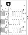
- FIG. 2 is a schematic illustrating a top view of an example of layer 105 from carrier chip 104.
- the layer 105 includes multiple co-planar circuit elements.
- layer 105 may include one or more co-planar waveguide resonators 202 for qubit readout.
- the co-planar waveguide resonators 202 include a center line 202a, which is separated from a ground plane 208 on either side by a constant width gap (denoted by the black lines surrounding center lines 202a in FIG. 2 ).
- the layer 105 includes one or more transmission lines 204.
- the transmission lines 204 may be configured and arranged near one or more of the co-planar waveguide resonators 202 so that the transmission lines 204 can electromagnetically couple to the resonators 202 during operation of the carrier chip.
- Layer 105 may further include interconnect pads arranged to make contact with the bump bonds between the first chip 102 and the second chip 104. Alternatively, or in addition, the interconnect pads may be electrically coupled to through-contacts arranged on or within the second chip.
- Layer 105 may further include wire-bond pads 206. Each of the interconnect pads and the wire-bond pads 206 may be fabricated by etching away predetermined portions of the superconductor material on the substrate surface 101 to form defined superconductor regions. Wire-bond pads 206 may be electrically connected to the transmission lines 204.
- the second chip 104 also includes second layer 107 formed on the second surface 103 of substrate 108, in which the second layer 107 includes components and/or materials that can cause relatively higher loss in quantum circuit elements (e.g., qubits) than the materials/components of the first layer 105.
- quantum circuit elements e.g., qubits
- the circuits formed within layer 107 are less likely to induce energy loss or decoherence in the quantum circuit elements of chip 102 or of layer 105.
- Layer 107 may include one or more layers of material.
- layer 107 may include one or more layers of a deposited dielectric 111, such as SiO 2 , SiN, or amorphous Si.
- Layer 107 may also include one or more layers of superconductor material 113, such as aluminum.
- layer 107 may include materials that do not function as superconductors, such as copper or silver. The materials of layer 107 may be patterned into one or more quantum or classical circuit elements.
- quantum or classical circuit elements examples include a resistor, an inductor, a capacitor (e.g., a parallel plate capacitor), a crossover wiring (e.g., an air-bridge connector), an amplifier (e.g., a traveling wave parametric amplifier), a resonator (e.g., an LC oscillator), or a Josephson logic circuit (e.g., an RSFQ device, and RQL device, or an ERSFQ device).
- a resistor an inductor
- a capacitor e.g., a parallel plate capacitor
- crossover wiring e.g., an air-bridge connector
- an amplifier e.g., a traveling wave parametric amplifier
- a resonator e.g., an LC oscillator
- a Josephson logic circuit e.g., an RSFQ device, and RQL device, or an ERSFQ device.
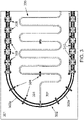
- FIG. 3 is a schematic illustrating a top view of an example of layer 107.
- layer 107 includes multiple circuit elements.
- layer 107 in the example includes a co-planar transmission line 302.
- the transmission line 302 includes a center line 302a formed from a superconductor material and may be separated from a ground plane 301.
- Layer 107 also includes dielectric crossovers 304 that provide a common electrical connection between the ground planes on either side of the center line 302a without electrically connecting to the center line 302a.
- Layer 107 also includes a co-planar waveguide resonator 306, parallel plate capacitors 308, and hybrid junction transmission lines 310.
- Fabrication of the parallel plate capacitors 308 and transmission lines 310 may include, e.g., deposition of a first layer of aluminum, followed by deposition of a dielectric layer, and then deposition of a second aluminum layer.
- a via opening may be established within the dielectric layer so that the second aluminum layer is deposited within the via and makes contact with the first aluminum layer after deposition.
- Multiple patterning (e.g., lithography and etching) steps may be required to define the different aluminum and dielectric layers.
- first layer 105 and second layer 107 are coupled (e.g., electrically connected) by one or more connectors 109 that extend from the first surface 101 to the second surface 103 of the substrate 108 of carrier chip 104.
- a connector 109 includes material that allows a low resistance electrical connection to be made be between one or more circuit elements of the first layer 105 and one or more circuit elements of the second layer 107.
- the second layer 107 includes an amplifier that is coupled to a measurement readout resonator through the connector 109. Accordingly, in some implementations, a signal used to probe the resonator may be routed from layer 105 through connector 109 to the amplifier of layer 107.
- the connector 109 examples include superconductor material such as aluminum or niobium.
- the connector 109 includes a material that is not a superconductor, but that still provides relatively low resistance, such as copper, tungsten or gold.
- the connectors 109 are located in a hole or via formed within the substrate 108.
- the hole or via in the substrate may be formed using, e.g., reactive ion etching or other suitable technique that allows a relatively constant area opening to be formed through the thickness of the substrate 108.
- the hole or via may be filled to form the through-hole connector 109. For instance, atomic layer deposition may be used to deposit tungsten or copper within the hole. Alternatively, or in addition, electroplating techniques may be used.
- connectors 109 are shown in FIG. 1 as extending through an opening in substrate 108, the connectors 109 alternatively (or additionally) may be formed so that they extend along an outer edge of the substrate 108, such that it is not necessary to form a hole within substrate 108.
- quantum computational systems may include, but is not limited to, quantum computers, quantum information processing systems, quantum cryptography systems, or quantum simulators.
- quantum information and quantum data refer to information or data that is carried by, held or stored in quantum systems, where the smallest non-trivial system is a qubit, e.g., a system that defines the unit of quantum information.
- qubit encompasses all quantum systems that may be suitably approximated as a two-level system in the corresponding context.
- Such quantum systems may include multi-level systems, e.g., with two or more levels.
- such systems can include atoms, electrons, photons, ions or superconducting qubits.
- the computational basis states are identified with the ground and first excited states, however it is understood that other setups where the computational states are identified with higher level excited states are possible.
- quantum memories are devices that can store quantum data for a long time with high fidelity and efficiency, e.g., light-matter interfaces where light is used for transmission and matter for storing and preserving the quantum features of quantum data such as superposition or quantum coherence.
- Quantum circuit elements may be used to perform quantum processing operations. That is, the quantum circuit elements may be configured to make use of quantum-mechanical phenomena, such as superposition and entanglement, to perform operations on data in a non-deterministic manner. Certain quantum circuit elements, such as qubits, may be configured to represent and operate on information in more than one state simultaneously. Examples of superconducting quantum circuit elements that may be formed with the processes disclosed herein include circuit elements such as co-planar waveguides, quantum LC oscillators, qubits (e.g., flux qubits or charge qubits), superconducting quantum interference devices (SQUIDs) (e.g., RF-SQUID or DC-SQUID), inductors, capacitors, transmission lines, ground planes, among others.
- qubits e.g., flux qubits or charge qubits
- SQUIDs superconducting quantum interference devices
- inductors capacitors, transmission lines, ground planes, among others.
- classical circuit elements generally process data in a deterministic manner.
- Classical circuit elements may be configured to collectively carry out instructions of a computer program by performing basic arithmetical, logical, and/or input/output operations on data, in which the data is represented in analog or digital form.
- classical circuit elements may be used to transmit data to and/or receive data from the quantum circuit elements through electrical or electromagnetic connections.
- Examples of classical circuit elements that may be formed with the processes disclosed herein include rapid single flux quantum (RSFQ) devices, reciprocal quantum logic (RQL) devices and ERSFQ devices, which are an energy-efficient version of RSFQ that does not use bias resistors.
- Other classical circuit elements may be formed with the processes disclosed herein as well.
- the superconducting circuit elements are cooled down within a cryostat to temperatures that allow a superconductor material to exhibit superconducting properties.
Landscapes
- Engineering & Computer Science (AREA)
- Theoretical Computer Science (AREA)
- Physics & Mathematics (AREA)
- General Physics & Mathematics (AREA)
- Computational Mathematics (AREA)
- Pure & Applied Mathematics (AREA)
- Data Mining & Analysis (AREA)
- Evolutionary Computation (AREA)
- Artificial Intelligence (AREA)
- Mathematical Analysis (AREA)
- Mathematical Optimization (AREA)
- Condensed Matter Physics & Semiconductors (AREA)
- Computing Systems (AREA)
- General Engineering & Computer Science (AREA)
- Mathematical Physics (AREA)
- Software Systems (AREA)
- Manufacturing & Machinery (AREA)
- Superconductor Devices And Manufacturing Methods Thereof (AREA)
Claims (10)
- Vorrichtung, umfassend:einen ersten Chip (102), der ein Qubit umfasst; undeinen zweiten Chip (104), der mit dem ersten Chip (102) verbunden ist, wobei der zweite Chip (104) ein Substrat (108) umfasst, das erste (101) und zweite (103) gegenüberliegende Oberflächen beinhaltet, wobei die erste Oberfläche (101) dem ersten Chip (102) zugewandt ist, wobei der zweite Chip (104) Folgendes umfasst:eine einzelne Schicht aus Supraleitermaterial (105) auf der ersten Oberfläche (101) des Substrats (108), wobei die einzelne Schicht aus Supraleitermaterial (105) ein erstes Schaltungselement umfasst,eine zweite Schicht (107) auf der zweiten Oberfläche (103) des Substrats (108), wobei die zweite Schicht (107) ein zweites Schaltungselement umfasst, undein Verbindungsstück (109), das sich von der ersten Oberfläche (101) des Substrats (108) zu der zweiten Oberfläche (103) des Substrats (108) erstreckt und einen Abschnitt der einzelnen Schicht aus Supraleitermaterial (105) elektrisch mit dem zweiten Schaltungselement verbindet,wobei die Vorrichtung einen Bump-Bond (106) zwischen dem ersten Chip (102) und der einzelnen Schicht aus Supraleitermaterial (105) umfasst,wobei der Bump-Bond (106) so angeordnet ist, dass er Daten zwischen dem Qubit auf dem ersten Chip (102) und dem ersten Schaltungselement koppelt, und wobei die einzelne Schicht aus Supraleitermaterial (105) einen Messwertausleseresonator (202) umfasst, der über den Bump-Bond (106) betriebsfähig mit dem Qubit des ersten Chips (102) gekoppelt ist.
- Vorrichtung nach Anspruch 1, wobei der Bump-Bond (106) Indium umfasst.
- Vorrichtung nach Anspruch 1, wobei kein festes dielektrisches Material in direktem Kontakt mit der ersten Oberfläche (101) des Substrats (108) oder in direktem Kontakt mit einer Oberfläche der einzelnen Schicht aus Supraleitermaterial (105), die dem ersten Chip (102) zugewandt ist, vorliegt.
- Vorrichtung nach Anspruch 1, wobei die einzelne Schicht aus Supraleitermaterial (105) eine Drahtbondkontaktstelle (112) umfasst.
- Vorrichtung nach Anspruch 4, wobei die einzelne Schicht aus Supraleitermaterial (105) eine Übertragungsleitung (204) umfasst, wobei die Drahtbondkontaktstelle (206) elektrisch mit der Übertragungsleitung (204) verbunden ist und die Übertragungsleitung (204) so angeordnet ist, dass sie elektromagnetisch oder elektrisch mit dem ersten Schaltungselement gekoppelt ist.
- Vorrichtung nach Anspruch 1, wobei sich das Verbindungsstück (109) durch eine Öffnung in dem Substrat (108) erstreckt.
- Vorrichtung nach Anspruch 1, wobei die zweite Schicht (107) mehrere Schichten aus Verdrahtung und dielektrischem Film umfasst.
- Vorrichtung nach Anspruch 1, wobei das zweite Schaltungselement einen Parallelplattenkondensator, eine Überkreuzungsverdrahtung, einen Verstärker, einen Resonator, eine Verdrahtung, die mehrere Schichten aus Supraleitermaterial umfasst, oder eine Josephson-Logikschaltung umfasst.
- Vorrichtung nach Anspruch 1, wobei eine Dicke des Bump-Bonds (106) zwischen der einzelnen Schicht aus Supraleitermaterial (105) und dem ersten Chip (102) zwischen 1 und 10 µm beträgt.
- Verfahren, umfassend:Bereitstellen eines ersten Chips (102), der ein Qubit umfasst;Bereitstellen eines zweiten Chips (104), der ein Substrat (108), eine einzelne Schicht aus Supraleitermaterial (105), die ein erstes Schaltungselement auf einer ersten Seite des Substrats (101) bildet, und ein zweites Schaltungselement auf einer zweiten Seite des Substrats (103), die der ersten Seite (101) gegenüberliegt, umfasst, wobei das zweite Schaltungselement elektrisch mit einem Abschnitt der einzelnen Schicht aus Supraleitermaterial (105) gekoppelt ist; undVerbinden des ersten Chips (102) mit dem zweiten Chip (104), sodass die Schicht aus Supraleitermaterial des zweiten Chips (105) dem ersten Chip (102) zugewandt ist,wobei das Verbinden des ersten Chips (102) mit dem zweiten Chip (104) ein Ausbilden eines Bump-Bonds (106) zwischen dem ersten Chip (102) und der einzelnen Schicht aus Supraleitermaterial (105) umfasst,wobei der Bump-Bond (106) so angeordnet ist, dass er Daten zwischen dem Qubit auf dem ersten Chip (102) und dem ersten Schaltungselement koppelt, undwobei die einzelne Schicht aus Supraleitermaterial (105) einen Messwertausleseresonator (202) umfasst, der über den Bump-Bond (106) betriebsfähig mit dem Qubit des ersten Chips (102) gekoppelt ist.
Priority Applications (1)
| Application Number | Priority Date | Filing Date | Title |
|---|---|---|---|
| EP22164248.1A EP4086965B1 (de) | 2016-09-13 | 2016-09-13 | Reduzierung des verlusts in gestapelten quantenvorrichtungen |
Applications Claiming Priority (1)
| Application Number | Priority Date | Filing Date | Title |
|---|---|---|---|
| PCT/US2016/051510 WO2018052399A1 (en) | 2016-09-13 | 2016-09-13 | Reducing loss in stacked quantum devices |
Related Child Applications (1)
| Application Number | Title | Priority Date | Filing Date |
|---|---|---|---|
| EP22164248.1A Division EP4086965B1 (de) | 2016-09-13 | 2016-09-13 | Reduzierung des verlusts in gestapelten quantenvorrichtungen |
Publications (2)
| Publication Number | Publication Date |
|---|---|
| EP3513434A1 EP3513434A1 (de) | 2019-07-24 |
| EP3513434B1 true EP3513434B1 (de) | 2022-04-13 |
Family
ID=57047306
Family Applications (2)
| Application Number | Title | Priority Date | Filing Date |
|---|---|---|---|
| EP16775387.0A Active EP3513434B1 (de) | 2016-09-13 | 2016-09-13 | Reduzierung des verlusts in gestapelten quantenvorrichtungen |
| EP22164248.1A Active EP4086965B1 (de) | 2016-09-13 | 2016-09-13 | Reduzierung des verlusts in gestapelten quantenvorrichtungen |
Family Applications After (1)
| Application Number | Title | Priority Date | Filing Date |
|---|---|---|---|
| EP22164248.1A Active EP4086965B1 (de) | 2016-09-13 | 2016-09-13 | Reduzierung des verlusts in gestapelten quantenvorrichtungen |
Country Status (7)
| Country | Link |
|---|---|
| US (3) | US10978425B2 (de) |
| EP (2) | EP3513434B1 (de) |
| JP (1) | JP6789385B2 (de) |
| KR (1) | KR102250155B1 (de) |
| CN (2) | CN117915758A (de) |
| CA (2) | CA3127307A1 (de) |
| WO (1) | WO2018052399A1 (de) |
Families Citing this family (32)
| Publication number | Priority date | Publication date | Assignee | Title |
|---|---|---|---|---|
| AU2017404530B2 (en) | 2017-03-13 | 2020-05-14 | Google Llc | Integrating circuit elements in a stacked quantum computing device |
| US11854833B2 (en) | 2018-07-30 | 2023-12-26 | Google Llc | Signal distribution for a quantum computing system |
| US10811588B2 (en) * | 2018-08-06 | 2020-10-20 | International Business Machines Corporation | Vertical dispersive readout of qubits of a lattice surface code architecture |
| US11121302B2 (en) * | 2018-10-11 | 2021-09-14 | SeeQC, Inc. | System and method for superconducting multi-chip module |
| US11957066B2 (en) * | 2019-09-04 | 2024-04-09 | Intel Corporation | Stackable in-line filter modules for quantum computing |
| US11158781B2 (en) | 2019-11-27 | 2021-10-26 | International Business Machines Corporation | Permanent wafer handlers with through silicon vias for thermalization and qubit modification |
| US11417819B2 (en) * | 2020-04-27 | 2022-08-16 | Microsoft Technology Licensing, Llc | Forming a bumpless superconductor device by bonding two substrates via a dielectric layer |
| CN115441147B (zh) * | 2020-05-29 | 2023-10-10 | 本源量子计算科技(合肥)股份有限公司 | 共面波导谐振器布图的构建方法、空气桥图层的构建方法 |
| EP3937093B1 (de) * | 2020-07-09 | 2024-09-04 | IQM Finland Oy | Quantenrechenschaltung mit einer vielzahl von chips und verfahren zu deren herstellung |
| FR3114444B1 (fr) | 2020-09-21 | 2022-09-30 | Commissariat Energie Atomique | Puce à routage bifonctionnel et procédé de fabrication associé |
| FR3114443B1 (fr) * | 2020-09-21 | 2022-12-23 | Commissariat Energie Atomique | Structure d’intégration à routage bifonctionnel et assemblage comprenant une telle structure |
| US11469485B2 (en) * | 2020-10-21 | 2022-10-11 | International Business Machines Corporation | Embedded microstrip transmission line |
| CN113707601A (zh) | 2020-11-20 | 2021-11-26 | 腾讯科技(深圳)有限公司 | 空气桥的制备方法、空气桥结构及超导量子芯片 |
| US20220199507A1 (en) * | 2020-12-22 | 2022-06-23 | International Business Machines Corporation | Multi-layered packaging for superconducting quantum circuits |
| CN114692881A (zh) * | 2020-12-31 | 2022-07-01 | 合肥本源量子计算科技有限责任公司 | 一种超导量子芯片结构 |
| WO2022143809A1 (zh) * | 2020-12-31 | 2022-07-07 | 合肥本源量子计算科技有限责任公司 | 超导量子芯片结构以及超导量子芯片制备方法 |
| CN115050886B (zh) * | 2021-03-09 | 2024-08-16 | 本源量子计算科技(合肥)股份有限公司 | 一种量子芯片及制备方法 |
| JP7806395B2 (ja) * | 2021-04-23 | 2026-01-27 | 日本電気株式会社 | 量子デバイス |
| CN118339566A (zh) | 2021-06-11 | 2024-07-12 | 西克公司 | 针对超导量子电路的通量偏置的系统和方法 |
| FR3125359B1 (fr) * | 2021-07-15 | 2024-08-16 | Commissariat Energie Atomique | Dispositif électronique destiné à connecter un premier composant électronique à un deuxième composant électronique, système comprenant un tel dispositif et procédés permettant d’obtenir un tel dispositif |
| CN113725208A (zh) * | 2021-08-13 | 2021-11-30 | 中国科学院物理研究所 | 一种三维量子芯片及其制备方法 |
| CN113793895B (zh) * | 2021-08-20 | 2023-01-06 | 宁波大学 | 一种squid芯片与磁显微镜探头及其封装方法 |
| CN114023733B (zh) * | 2021-11-03 | 2025-05-30 | 材料科学姑苏实验室 | 一种超导量子芯片的三维封装结构及封装方法 |
| FR3129772B1 (fr) | 2021-11-30 | 2024-10-04 | Commissariat Energie Atomique | Structure d’intégration destinée à connecter une pluralité de dispositifs semi-conducteurs, procédés, assemblage et système associés |
| WO2023132063A1 (ja) * | 2022-01-07 | 2023-07-13 | 富士通株式会社 | 量子演算装置及び量子演算装置の製造方法 |
| EP4730215A2 (de) * | 2022-01-07 | 2026-04-22 | Fujitsu Limited | Verfahren zur herstellung einer quantencomputervorrichtung |
| US12501841B2 (en) | 2022-04-15 | 2025-12-16 | International Business Machines Corporation | High density interconnects for arrays of Josephson traveling wave parametric devices |
| JP2024046522A (ja) * | 2022-09-22 | 2024-04-03 | 国立研究開発法人産業技術総合研究所 | 回路、超伝導装置及び回路の製造方法 |
| US20240194661A1 (en) * | 2022-12-13 | 2024-06-13 | Google Llc | Multi-layer chip architecture and fabrication |
| US20240194532A1 (en) * | 2022-12-13 | 2024-06-13 | Google Llc | Multi-layer chip architecture and fabrication |
| CN115630702B (zh) * | 2022-12-23 | 2023-03-28 | 材料科学姑苏实验室 | 一种多层超导量子芯片 |
| WO2025143502A1 (ko) * | 2023-12-29 | 2025-07-03 | (재)한국나노기술원 | 초전도 양자큐비트 소자 및 그 제조방법 |
Citations (1)
| Publication number | Priority date | Publication date | Assignee | Title |
|---|---|---|---|---|
| EP3391415B1 (de) * | 2015-12-15 | 2019-08-21 | Google LLC | Supraleitende bump-bonds |
Family Cites Families (20)
| Publication number | Priority date | Publication date | Assignee | Title |
|---|---|---|---|---|
| JPH09252026A (ja) * | 1992-04-06 | 1997-09-22 | Seiko Instr Inc | 超伝導装置 |
| JPH08504541A (ja) | 1992-12-15 | 1996-05-14 | イー・アイ・デユポン・ドウ・ヌムール・アンド・カンパニー | 電気的相互接続構造 |
| JP4130065B2 (ja) * | 2000-03-27 | 2008-08-06 | 株式会社日立製作所 | 超電導量子干渉素子及び超電導回路 |
| US6614047B2 (en) * | 2001-12-17 | 2003-09-02 | D-Wave Systems, Inc. | Finger squid qubit device |
| US7075171B2 (en) * | 2003-03-11 | 2006-07-11 | Fujitsu Limited | Superconducting system, superconducting circuit chip, and high-temperature superconducting junction device with a shunt resistor |
| JP2004303820A (ja) * | 2003-03-28 | 2004-10-28 | Fujitsu Ltd | 超伝導回路 |
| US6917537B2 (en) * | 2003-08-11 | 2005-07-12 | Northrop Grumman Corporation | RSFQ Batcher-banyan switching network |
| US7932515B2 (en) | 2008-01-03 | 2011-04-26 | D-Wave Systems Inc. | Quantum processor |
| US8138880B2 (en) * | 2008-07-30 | 2012-03-20 | International Business Machines Corporation | Persistent current switch |
| EP3098865B1 (de) * | 2009-02-27 | 2018-10-03 | D-Wave Systems Inc. | Verfahren zur herstellung einer supraleitenden integrierten schaltung |
| US9780764B2 (en) * | 2010-04-05 | 2017-10-03 | Northrop Grumman Systems Corporation | Phase quantum bit |
| US8852959B2 (en) | 2011-12-19 | 2014-10-07 | Northrup Grumman Systems Corporation | Low temperature resistor for superconductor circuits |
| WO2013180780A2 (en) * | 2012-03-08 | 2013-12-05 | D-Wave Systems Inc. | Systems and methods for fabrication of superconducting integrated circuits |
| EP2946413B1 (de) * | 2013-01-18 | 2022-01-05 | Yale University | Supraleitende vorrichtung mit mindestens einem gehäuse |
| US9881904B2 (en) * | 2014-11-05 | 2018-01-30 | Massachusetts Institute Of Technology | Multi-layer semiconductor devices fabricated using a combination of substrate and via structures and fabrication techniques |
| US9836699B1 (en) * | 2015-04-27 | 2017-12-05 | Rigetti & Co. | Microwave integrated quantum circuits with interposer |
| US10134972B2 (en) * | 2015-07-23 | 2018-11-20 | Massachusetts Institute Of Technology | Qubit and coupler circuit structures and coupling techniques |
| WO2017015432A1 (en) * | 2015-07-23 | 2017-01-26 | Massachusetts Institute Of Technology | Superconducting integrated circuit |
| US10396269B2 (en) * | 2015-11-05 | 2019-08-27 | Massachusetts Institute Of Technology | Interconnect structures for assembly of semiconductor structures including superconducting integrated circuits |
| US20190131511A1 (en) * | 2016-06-30 | 2019-05-02 | Intel Corporation | Superconductor-silicon interface control |
-
2016
- 2016-09-13 WO PCT/US2016/051510 patent/WO2018052399A1/en not_active Ceased
- 2016-09-13 EP EP16775387.0A patent/EP3513434B1/de active Active
- 2016-09-13 JP JP2019513972A patent/JP6789385B2/ja active Active
- 2016-09-13 CN CN202311781957.XA patent/CN117915758A/zh active Pending
- 2016-09-13 KR KR1020197010613A patent/KR102250155B1/ko active Active
- 2016-09-13 US US16/333,020 patent/US10978425B2/en active Active
- 2016-09-13 CN CN201680089250.4A patent/CN109891591B/zh active Active
- 2016-09-13 EP EP22164248.1A patent/EP4086965B1/de active Active
- 2016-09-13 CA CA3127307A patent/CA3127307A1/en active Pending
- 2016-09-13 CA CA3036054A patent/CA3036054C/en active Active
-
2021
- 2021-04-12 US US17/228,393 patent/US11569205B2/en active Active
-
2023
- 2023-01-30 US US18/103,227 patent/US11955465B2/en active Active
Patent Citations (1)
| Publication number | Priority date | Publication date | Assignee | Title |
|---|---|---|---|---|
| EP3391415B1 (de) * | 2015-12-15 | 2019-08-21 | Google LLC | Supraleitende bump-bonds |
Also Published As
| Publication number | Publication date |
|---|---|
| CN109891591B (zh) | 2024-01-09 |
| CN109891591A (zh) | 2019-06-14 |
| EP4086965A1 (de) | 2022-11-09 |
| JP2019532505A (ja) | 2019-11-07 |
| US11569205B2 (en) | 2023-01-31 |
| US20190229094A1 (en) | 2019-07-25 |
| WO2018052399A1 (en) | 2018-03-22 |
| KR102250155B1 (ko) | 2021-05-10 |
| US10978425B2 (en) | 2021-04-13 |
| KR20190045362A (ko) | 2019-05-02 |
| CA3127307A1 (en) | 2018-03-22 |
| US20230178519A1 (en) | 2023-06-08 |
| US20210233896A1 (en) | 2021-07-29 |
| CA3036054A1 (en) | 2018-03-22 |
| CA3036054C (en) | 2021-10-19 |
| EP3513434A1 (de) | 2019-07-24 |
| JP6789385B2 (ja) | 2020-11-25 |
| US11955465B2 (en) | 2024-04-09 |
| CN117915758A (zh) | 2024-04-19 |
| EP4086965B1 (de) | 2025-08-20 |
Similar Documents
| Publication | Publication Date | Title |
|---|---|---|
| US11955465B2 (en) | Reducing loss in stacked quantum devices | |
| US12217129B2 (en) | Integrating circuit elements in a stacked quantum computing device | |
| US11133451B2 (en) | Superconducting bump bonds | |
| US12120966B2 (en) | Low footprint resonator in flip chip geometry | |
| CN110176532A (zh) | 用于量子位器件的具有顶部超导体层的封装衬底 | |
| EP4617958A1 (de) | Flussleitungserdung für quantenprozessor |
Legal Events
| Date | Code | Title | Description |
|---|---|---|---|
| STAA | Information on the status of an ep patent application or granted ep patent |
Free format text: STATUS: THE INTERNATIONAL PUBLICATION HAS BEEN MADE |
|
| PUAI | Public reference made under article 153(3) epc to a published international application that has entered the european phase |
Free format text: ORIGINAL CODE: 0009012 |
|
| STAA | Information on the status of an ep patent application or granted ep patent |
Free format text: STATUS: REQUEST FOR EXAMINATION WAS MADE |
|
| 17P | Request for examination filed |
Effective date: 20190415 |
|
| AK | Designated contracting states |
Kind code of ref document: A1 Designated state(s): AL AT BE BG CH CY CZ DE DK EE ES FI FR GB GR HR HU IE IS IT LI LT LU LV MC MK MT NL NO PL PT RO RS SE SI SK SM TR |
|
| AX | Request for extension of the european patent |
Extension state: BA ME |
|
| DAV | Request for validation of the european patent (deleted) | ||
| DAX | Request for extension of the european patent (deleted) | ||
| STAA | Information on the status of an ep patent application or granted ep patent |
Free format text: STATUS: EXAMINATION IS IN PROGRESS |
|
| 17Q | First examination report despatched |
Effective date: 20201001 |
|
| GRAP | Despatch of communication of intention to grant a patent |
Free format text: ORIGINAL CODE: EPIDOSNIGR1 |
|
| STAA | Information on the status of an ep patent application or granted ep patent |
Free format text: STATUS: GRANT OF PATENT IS INTENDED |
|
| GRAJ | Information related to disapproval of communication of intention to grant by the applicant or resumption of examination proceedings by the epo deleted |
Free format text: ORIGINAL CODE: EPIDOSDIGR1 |
|
| RIC1 | Information provided on ipc code assigned before grant |
Ipc: G06N 10/00 20190101ALI20210914BHEP Ipc: H01L 23/00 20060101ALI20210914BHEP Ipc: H01L 25/065 20060101ALI20210914BHEP Ipc: H01L 27/18 20060101AFI20210914BHEP |
|
| GRAP | Despatch of communication of intention to grant a patent |
Free format text: ORIGINAL CODE: EPIDOSNIGR1 |
|
| INTG | Intention to grant announced |
Effective date: 20211014 |
|
| INTG | Intention to grant announced |
Effective date: 20211027 |
|
| GRAS | Grant fee paid |
Free format text: ORIGINAL CODE: EPIDOSNIGR3 |
|
| GRAA | (expected) grant |
Free format text: ORIGINAL CODE: 0009210 |
|
| STAA | Information on the status of an ep patent application or granted ep patent |
Free format text: STATUS: THE PATENT HAS BEEN GRANTED |
|
| AK | Designated contracting states |
Kind code of ref document: B1 Designated state(s): AL AT BE BG CH CY CZ DE DK EE ES FI FR GB GR HR HU IE IS IT LI LT LU LV MC MK MT NL NO PL PT RO RS SE SI SK SM TR |
|
| REG | Reference to a national code |
Ref country code: GB Ref legal event code: FG4D |
|
| REG | Reference to a national code |
Ref country code: CH Ref legal event code: EP |
|
| REG | Reference to a national code |
Ref country code: DE Ref legal event code: R096 Ref document number: 602016071067 Country of ref document: DE |
|
| REG | Reference to a national code |
Ref country code: IE Ref legal event code: FG4D |
|
| REG | Reference to a national code |
Ref country code: AT Ref legal event code: REF Ref document number: 1484087 Country of ref document: AT Kind code of ref document: T Effective date: 20220515 |
|
| REG | Reference to a national code |
Ref country code: LT Ref legal event code: MG9D |
|
| REG | Reference to a national code |
Ref country code: NL Ref legal event code: MP Effective date: 20220413 |
|
| REG | Reference to a national code |
Ref country code: AT Ref legal event code: MK05 Ref document number: 1484087 Country of ref document: AT Kind code of ref document: T Effective date: 20220413 |
|
| PG25 | Lapsed in a contracting state [announced via postgrant information from national office to epo] |
Ref country code: NL Free format text: LAPSE BECAUSE OF FAILURE TO SUBMIT A TRANSLATION OF THE DESCRIPTION OR TO PAY THE FEE WITHIN THE PRESCRIBED TIME-LIMIT Effective date: 20220413 |
|
| PG25 | Lapsed in a contracting state [announced via postgrant information from national office to epo] |
Ref country code: SE Free format text: LAPSE BECAUSE OF FAILURE TO SUBMIT A TRANSLATION OF THE DESCRIPTION OR TO PAY THE FEE WITHIN THE PRESCRIBED TIME-LIMIT Effective date: 20220413 Ref country code: PT Free format text: LAPSE BECAUSE OF FAILURE TO SUBMIT A TRANSLATION OF THE DESCRIPTION OR TO PAY THE FEE WITHIN THE PRESCRIBED TIME-LIMIT Effective date: 20220816 Ref country code: NO Free format text: LAPSE BECAUSE OF FAILURE TO SUBMIT A TRANSLATION OF THE DESCRIPTION OR TO PAY THE FEE WITHIN THE PRESCRIBED TIME-LIMIT Effective date: 20220713 Ref country code: LT Free format text: LAPSE BECAUSE OF FAILURE TO SUBMIT A TRANSLATION OF THE DESCRIPTION OR TO PAY THE FEE WITHIN THE PRESCRIBED TIME-LIMIT Effective date: 20220413 Ref country code: HR Free format text: LAPSE BECAUSE OF FAILURE TO SUBMIT A TRANSLATION OF THE DESCRIPTION OR TO PAY THE FEE WITHIN THE PRESCRIBED TIME-LIMIT Effective date: 20220413 Ref country code: GR Free format text: LAPSE BECAUSE OF FAILURE TO SUBMIT A TRANSLATION OF THE DESCRIPTION OR TO PAY THE FEE WITHIN THE PRESCRIBED TIME-LIMIT Effective date: 20220714 Ref country code: FI Free format text: LAPSE BECAUSE OF FAILURE TO SUBMIT A TRANSLATION OF THE DESCRIPTION OR TO PAY THE FEE WITHIN THE PRESCRIBED TIME-LIMIT Effective date: 20220413 Ref country code: ES Free format text: LAPSE BECAUSE OF FAILURE TO SUBMIT A TRANSLATION OF THE DESCRIPTION OR TO PAY THE FEE WITHIN THE PRESCRIBED TIME-LIMIT Effective date: 20220413 Ref country code: BG Free format text: LAPSE BECAUSE OF FAILURE TO SUBMIT A TRANSLATION OF THE DESCRIPTION OR TO PAY THE FEE WITHIN THE PRESCRIBED TIME-LIMIT Effective date: 20220713 Ref country code: AT Free format text: LAPSE BECAUSE OF FAILURE TO SUBMIT A TRANSLATION OF THE DESCRIPTION OR TO PAY THE FEE WITHIN THE PRESCRIBED TIME-LIMIT Effective date: 20220413 |
|
| REG | Reference to a national code |
Ref country code: DE Ref legal event code: R079 Ref document number: 602016071067 Country of ref document: DE Free format text: PREVIOUS MAIN CLASS: H01L0027180000 Ipc: H10N0069000000 |
|
| PG25 | Lapsed in a contracting state [announced via postgrant information from national office to epo] |
Ref country code: RS Free format text: LAPSE BECAUSE OF FAILURE TO SUBMIT A TRANSLATION OF THE DESCRIPTION OR TO PAY THE FEE WITHIN THE PRESCRIBED TIME-LIMIT Effective date: 20220413 Ref country code: PL Free format text: LAPSE BECAUSE OF FAILURE TO SUBMIT A TRANSLATION OF THE DESCRIPTION OR TO PAY THE FEE WITHIN THE PRESCRIBED TIME-LIMIT Effective date: 20220413 Ref country code: LV Free format text: LAPSE BECAUSE OF FAILURE TO SUBMIT A TRANSLATION OF THE DESCRIPTION OR TO PAY THE FEE WITHIN THE PRESCRIBED TIME-LIMIT Effective date: 20220413 Ref country code: IS Free format text: LAPSE BECAUSE OF FAILURE TO SUBMIT A TRANSLATION OF THE DESCRIPTION OR TO PAY THE FEE WITHIN THE PRESCRIBED TIME-LIMIT Effective date: 20220813 |
|
| REG | Reference to a national code |
Ref country code: DE Ref legal event code: R097 Ref document number: 602016071067 Country of ref document: DE |
|
| PG25 | Lapsed in a contracting state [announced via postgrant information from national office to epo] |
Ref country code: SM Free format text: LAPSE BECAUSE OF FAILURE TO SUBMIT A TRANSLATION OF THE DESCRIPTION OR TO PAY THE FEE WITHIN THE PRESCRIBED TIME-LIMIT Effective date: 20220413 Ref country code: SK Free format text: LAPSE BECAUSE OF FAILURE TO SUBMIT A TRANSLATION OF THE DESCRIPTION OR TO PAY THE FEE WITHIN THE PRESCRIBED TIME-LIMIT Effective date: 20220413 Ref country code: RO Free format text: LAPSE BECAUSE OF FAILURE TO SUBMIT A TRANSLATION OF THE DESCRIPTION OR TO PAY THE FEE WITHIN THE PRESCRIBED TIME-LIMIT Effective date: 20220413 Ref country code: EE Free format text: LAPSE BECAUSE OF FAILURE TO SUBMIT A TRANSLATION OF THE DESCRIPTION OR TO PAY THE FEE WITHIN THE PRESCRIBED TIME-LIMIT Effective date: 20220413 Ref country code: DK Free format text: LAPSE BECAUSE OF FAILURE TO SUBMIT A TRANSLATION OF THE DESCRIPTION OR TO PAY THE FEE WITHIN THE PRESCRIBED TIME-LIMIT Effective date: 20220413 Ref country code: CZ Free format text: LAPSE BECAUSE OF FAILURE TO SUBMIT A TRANSLATION OF THE DESCRIPTION OR TO PAY THE FEE WITHIN THE PRESCRIBED TIME-LIMIT Effective date: 20220413 |
|
| PLBE | No opposition filed within time limit |
Free format text: ORIGINAL CODE: 0009261 |
|
| STAA | Information on the status of an ep patent application or granted ep patent |
Free format text: STATUS: NO OPPOSITION FILED WITHIN TIME LIMIT |
|
| 26N | No opposition filed |
Effective date: 20230116 |
|
| PG25 | Lapsed in a contracting state [announced via postgrant information from national office to epo] |
Ref country code: AL Free format text: LAPSE BECAUSE OF FAILURE TO SUBMIT A TRANSLATION OF THE DESCRIPTION OR TO PAY THE FEE WITHIN THE PRESCRIBED TIME-LIMIT Effective date: 20220413 |
|
| PG25 | Lapsed in a contracting state [announced via postgrant information from national office to epo] |
Ref country code: MC Free format text: LAPSE BECAUSE OF FAILURE TO SUBMIT A TRANSLATION OF THE DESCRIPTION OR TO PAY THE FEE WITHIN THE PRESCRIBED TIME-LIMIT Effective date: 20220413 |
|
| REG | Reference to a national code |
Ref country code: CH Ref legal event code: PL |
|
| REG | Reference to a national code |
Ref country code: BE Ref legal event code: MM Effective date: 20220930 |
|
| PG25 | Lapsed in a contracting state [announced via postgrant information from national office to epo] |
Ref country code: SI Free format text: LAPSE BECAUSE OF FAILURE TO SUBMIT A TRANSLATION OF THE DESCRIPTION OR TO PAY THE FEE WITHIN THE PRESCRIBED TIME-LIMIT Effective date: 20220413 |
|
| P01 | Opt-out of the competence of the unified patent court (upc) registered |
Effective date: 20230510 |
|
| PG25 | Lapsed in a contracting state [announced via postgrant information from national office to epo] |
Ref country code: LU Free format text: LAPSE BECAUSE OF NON-PAYMENT OF DUE FEES Effective date: 20220913 |
|
| PG25 | Lapsed in a contracting state [announced via postgrant information from national office to epo] |
Ref country code: LI Free format text: LAPSE BECAUSE OF NON-PAYMENT OF DUE FEES Effective date: 20220930 Ref country code: IE Free format text: LAPSE BECAUSE OF NON-PAYMENT OF DUE FEES Effective date: 20220913 Ref country code: CH Free format text: LAPSE BECAUSE OF NON-PAYMENT OF DUE FEES Effective date: 20220930 |
|
| PG25 | Lapsed in a contracting state [announced via postgrant information from national office to epo] |
Ref country code: BE Free format text: LAPSE BECAUSE OF NON-PAYMENT OF DUE FEES Effective date: 20220930 |
|
| PG25 | Lapsed in a contracting state [announced via postgrant information from national office to epo] |
Ref country code: IT Free format text: LAPSE BECAUSE OF FAILURE TO SUBMIT A TRANSLATION OF THE DESCRIPTION OR TO PAY THE FEE WITHIN THE PRESCRIBED TIME-LIMIT Effective date: 20220413 |
|
| PG25 | Lapsed in a contracting state [announced via postgrant information from national office to epo] |
Ref country code: HU Free format text: LAPSE BECAUSE OF FAILURE TO SUBMIT A TRANSLATION OF THE DESCRIPTION OR TO PAY THE FEE WITHIN THE PRESCRIBED TIME-LIMIT; INVALID AB INITIO Effective date: 20160913 |
|
| PG25 | Lapsed in a contracting state [announced via postgrant information from national office to epo] |
Ref country code: CY Free format text: LAPSE BECAUSE OF FAILURE TO SUBMIT A TRANSLATION OF THE DESCRIPTION OR TO PAY THE FEE WITHIN THE PRESCRIBED TIME-LIMIT Effective date: 20220413 |
|
| PG25 | Lapsed in a contracting state [announced via postgrant information from national office to epo] |
Ref country code: MK Free format text: LAPSE BECAUSE OF FAILURE TO SUBMIT A TRANSLATION OF THE DESCRIPTION OR TO PAY THE FEE WITHIN THE PRESCRIBED TIME-LIMIT Effective date: 20220413 |
|
| PG25 | Lapsed in a contracting state [announced via postgrant information from national office to epo] |
Ref country code: MT Free format text: LAPSE BECAUSE OF FAILURE TO SUBMIT A TRANSLATION OF THE DESCRIPTION OR TO PAY THE FEE WITHIN THE PRESCRIBED TIME-LIMIT Effective date: 20220413 |
|
| PG25 | Lapsed in a contracting state [announced via postgrant information from national office to epo] |
Ref country code: BG Free format text: LAPSE BECAUSE OF FAILURE TO SUBMIT A TRANSLATION OF THE DESCRIPTION OR TO PAY THE FEE WITHIN THE PRESCRIBED TIME-LIMIT Effective date: 20220413 |
|
| PG25 | Lapsed in a contracting state [announced via postgrant information from national office to epo] |
Ref country code: BG Free format text: LAPSE BECAUSE OF FAILURE TO SUBMIT A TRANSLATION OF THE DESCRIPTION OR TO PAY THE FEE WITHIN THE PRESCRIBED TIME-LIMIT Effective date: 20220413 |
|
| PGFP | Annual fee paid to national office [announced via postgrant information from national office to epo] |
Ref country code: DE Payment date: 20250929 Year of fee payment: 10 |
|
| PGFP | Annual fee paid to national office [announced via postgrant information from national office to epo] |
Ref country code: GB Payment date: 20250929 Year of fee payment: 10 |
|
| PGFP | Annual fee paid to national office [announced via postgrant information from national office to epo] |
Ref country code: FR Payment date: 20250925 Year of fee payment: 10 |
|
| PG25 | Lapsed in a contracting state [announced via postgrant information from national office to epo] |
Ref country code: TR Free format text: LAPSE BECAUSE OF FAILURE TO SUBMIT A TRANSLATION OF THE DESCRIPTION OR TO PAY THE FEE WITHIN THE PRESCRIBED TIME-LIMIT Effective date: 20220413 |