EP3487266B1 - Micro led array display device - Google Patents
Micro led array display device Download PDFInfo
- Publication number
- EP3487266B1 EP3487266B1 EP17831202.1A EP17831202A EP3487266B1 EP 3487266 B1 EP3487266 B1 EP 3487266B1 EP 17831202 A EP17831202 A EP 17831202A EP 3487266 B1 EP3487266 B1 EP 3487266B1
- Authority
- EP
- European Patent Office
- Prior art keywords
- micro
- led
- conductivity
- pixels
- cmos
- Prior art date
- Legal status (The legal status is an assumption and is not a legal conclusion. Google has not performed a legal analysis and makes no representation as to the accuracy of the status listed.)
- Active
Links
Images


Classifications
-
- H—ELECTRICITY
- H05—ELECTRIC TECHNIQUES NOT OTHERWISE PROVIDED FOR
- H05B—ELECTRIC HEATING; ELECTRIC LIGHT SOURCES NOT OTHERWISE PROVIDED FOR; CIRCUIT ARRANGEMENTS FOR ELECTRIC LIGHT SOURCES, IN GENERAL
- H05B33/00—Electroluminescent light sources
- H05B33/10—Apparatus or processes specially adapted to the manufacture of electroluminescent light sources
-
- H—ELECTRICITY
- H10—SEMICONDUCTOR DEVICES; ELECTRIC SOLID-STATE DEVICES NOT OTHERWISE PROVIDED FOR
- H10W—GENERIC PACKAGES, INTERCONNECTIONS, CONNECTORS OR OTHER CONSTRUCTIONAL DETAILS OF DEVICES COVERED BY CLASS H10
- H10W90/00—Package configurations
-
- H—ELECTRICITY
- H05—ELECTRIC TECHNIQUES NOT OTHERWISE PROVIDED FOR
- H05B—ELECTRIC HEATING; ELECTRIC LIGHT SOURCES NOT OTHERWISE PROVIDED FOR; CIRCUIT ARRANGEMENTS FOR ELECTRIC LIGHT SOURCES, IN GENERAL
- H05B33/00—Electroluminescent light sources
- H05B33/12—Light sources with substantially two-dimensional [2D] radiating surfaces
-
- H—ELECTRICITY
- H10—SEMICONDUCTOR DEVICES; ELECTRIC SOLID-STATE DEVICES NOT OTHERWISE PROVIDED FOR
- H10H—INORGANIC LIGHT-EMITTING SEMICONDUCTOR DEVICES HAVING POTENTIAL BARRIERS
- H10H20/00—Individual inorganic light-emitting semiconductor devices having potential barriers, e.g. light-emitting diodes [LED]
- H10H20/80—Constructional details
- H10H20/81—Bodies
-
- H—ELECTRICITY
- H10—SEMICONDUCTOR DEVICES; ELECTRIC SOLID-STATE DEVICES NOT OTHERWISE PROVIDED FOR
- H10H—INORGANIC LIGHT-EMITTING SEMICONDUCTOR DEVICES HAVING POTENTIAL BARRIERS
- H10H20/00—Individual inorganic light-emitting semiconductor devices having potential barriers, e.g. light-emitting diodes [LED]
- H10H20/80—Constructional details
- H10H20/83—Electrodes
-
- H—ELECTRICITY
- H10—SEMICONDUCTOR DEVICES; ELECTRIC SOLID-STATE DEVICES NOT OTHERWISE PROVIDED FOR
- H10H—INORGANIC LIGHT-EMITTING SEMICONDUCTOR DEVICES HAVING POTENTIAL BARRIERS
- H10H20/00—Individual inorganic light-emitting semiconductor devices having potential barriers, e.g. light-emitting diodes [LED]
- H10H20/80—Constructional details
- H10H20/83—Electrodes
- H10H20/831—Electrodes characterised by their shape
- H10H20/8312—Electrodes characterised by their shape extending at least partially through the bodies
-
- H—ELECTRICITY
- H10—SEMICONDUCTOR DEVICES; ELECTRIC SOLID-STATE DEVICES NOT OTHERWISE PROVIDED FOR
- H10H—INORGANIC LIGHT-EMITTING SEMICONDUCTOR DEVICES HAVING POTENTIAL BARRIERS
- H10H20/00—Individual inorganic light-emitting semiconductor devices having potential barriers, e.g. light-emitting diodes [LED]
- H10H20/80—Constructional details
- H10H20/85—Packages
- H10H20/857—Interconnections, e.g. lead-frames, bond wires or solder balls
-
- H—ELECTRICITY
- H10—SEMICONDUCTOR DEVICES; ELECTRIC SOLID-STATE DEVICES NOT OTHERWISE PROVIDED FOR
- H10H—INORGANIC LIGHT-EMITTING SEMICONDUCTOR DEVICES HAVING POTENTIAL BARRIERS
- H10H29/00—Integrated devices, or assemblies of multiple devices, comprising at least one light-emitting semiconductor element covered by group H10H20/00
- H10H29/10—Integrated devices comprising at least one light-emitting semiconductor component covered by group H10H20/00
- H10H29/14—Integrated devices comprising at least one light-emitting semiconductor component covered by group H10H20/00 comprising multiple light-emitting semiconductor components
- H10H29/142—Two-dimensional arrangements, e.g. asymmetric LED layout
-
- H—ELECTRICITY
- H10—SEMICONDUCTOR DEVICES; ELECTRIC SOLID-STATE DEVICES NOT OTHERWISE PROVIDED FOR
- H10W—GENERIC PACKAGES, INTERCONNECTIONS, CONNECTORS OR OTHER CONSTRUCTIONAL DETAILS OF DEVICES COVERED BY CLASS H10
- H10W72/00—Interconnections or connectors in packages
- H10W72/20—Bump connectors, e.g. solder bumps or copper pillars; Dummy bumps; Thermal bumps
-
- H—ELECTRICITY
- H10—SEMICONDUCTOR DEVICES; ELECTRIC SOLID-STATE DEVICES NOT OTHERWISE PROVIDED FOR
- H10D—INORGANIC ELECTRIC SEMICONDUCTOR DEVICES
- H10D86/00—Integrated devices formed in or on insulating or conducting substrates, e.g. formed in silicon-on-insulator [SOI] substrates or on stainless steel or glass substrates
- H10D86/40—Integrated devices formed in or on insulating or conducting substrates, e.g. formed in silicon-on-insulator [SOI] substrates or on stainless steel or glass substrates characterised by multiple TFTs
- H10D86/411—Integrated devices formed in or on insulating or conducting substrates, e.g. formed in silicon-on-insulator [SOI] substrates or on stainless steel or glass substrates characterised by multiple TFTs characterised by materials, geometry or structure of the substrates
-
- H—ELECTRICITY
- H10—SEMICONDUCTOR DEVICES; ELECTRIC SOLID-STATE DEVICES NOT OTHERWISE PROVIDED FOR
- H10D—INORGANIC ELECTRIC SEMICONDUCTOR DEVICES
- H10D86/00—Integrated devices formed in or on insulating or conducting substrates, e.g. formed in silicon-on-insulator [SOI] substrates or on stainless steel or glass substrates
- H10D86/40—Integrated devices formed in or on insulating or conducting substrates, e.g. formed in silicon-on-insulator [SOI] substrates or on stainless steel or glass substrates characterised by multiple TFTs
- H10D86/441—Interconnections, e.g. scanning lines
-
- H—ELECTRICITY
- H10—SEMICONDUCTOR DEVICES; ELECTRIC SOLID-STATE DEVICES NOT OTHERWISE PROVIDED FOR
- H10D—INORGANIC ELECTRIC SEMICONDUCTOR DEVICES
- H10D86/00—Integrated devices formed in or on insulating or conducting substrates, e.g. formed in silicon-on-insulator [SOI] substrates or on stainless steel or glass substrates
- H10D86/40—Integrated devices formed in or on insulating or conducting substrates, e.g. formed in silicon-on-insulator [SOI] substrates or on stainless steel or glass substrates characterised by multiple TFTs
- H10D86/60—Integrated devices formed in or on insulating or conducting substrates, e.g. formed in silicon-on-insulator [SOI] substrates or on stainless steel or glass substrates characterised by multiple TFTs wherein the TFTs are in active matrices
-
- H—ELECTRICITY
- H10—SEMICONDUCTOR DEVICES; ELECTRIC SOLID-STATE DEVICES NOT OTHERWISE PROVIDED FOR
- H10H—INORGANIC LIGHT-EMITTING SEMICONDUCTOR DEVICES HAVING POTENTIAL BARRIERS
- H10H20/00—Individual inorganic light-emitting semiconductor devices having potential barriers, e.g. light-emitting diodes [LED]
- H10H20/01—Manufacture or treatment
- H10H20/036—Manufacture or treatment of packages
- H10H20/0364—Manufacture or treatment of packages of interconnections
Definitions
- One object of the present invention is to provide a micro-LED array display device according to claim 1, wherein micro-LED pixels are flip-chip bonded to corresponding CMOS cells formed on a CMOS backplane through bumps, thus avoiding the complexity and inconvenience of wire bonding for connecting micro-LED pixels to various data lines while enabling individual control of the micro-LED pixels.
- a further object of the present invention is to provide a micro-LED array display device according to claim 4, wherein micro-LED panels, each including a plurality of micro-LED pixels, are flip-chip bonded to a single CMOS backplane, thus overcoming the difficulties of the prior art in forming red, green, and blue light emitting structures including micro-LED pixels formed on one substrate.
- the first conductivity-type metal layer functions as a common electrode of the micro-LED pixels.
- the first conductivity-type is n-type and the second conductivity-type is p-type.
- the substrate is made of a material selected from sapphire, SiC, Si, glass, and ZnO.
- the bumps are formed on the CMOS cells and are melted by heating such that the CMOS cells are electrically connected to the corresponding micro-LED pixels.
- micro-LED pixels are flip-chip bonded to micro-LED pixels formed on a CMOS backplane through bumps, avoiding the complexity and inconvenience of wire bonding for connecting micro-LED pixels to various data lines while enabling individual control of the micro-LED pixels.
- the micro-LED array display device of an embodiment in which a plurality of micro-LED panels emitting red, green, and blue light are flip-chip bonded to a single CMOS backplane through bumps can focus three colors on the same area using an optical system to achieve full color. Therefore, the micro-LED array display device of the embodiment is effective in overcoming the technical difficulties of the prior art in forming red, green, and blue light emitting structures including a plurality of micro-LED pixels on one substrate.
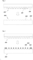
- Fig. 1 illustrates an exemplary micro-LED panel 100 of a micro-LED array display device according to one embodiment
- Fig. 2 illustrates the micro-LED panel 100 including micro-LED pixels and a CMOS backplane 200 including a plurality of CMOS cells adapted to individually drive the micro-LED pixels of the micro-LED panel 100
- Fig. 3 illustrates a state in which the micro-LED panel 100 and the CMOS backplane 200 are electrically connected to each other through bumps 300 arranged on the CMOS backplane 200
- Fig. 1 illustrates an exemplary micro-LED panel 100 of a micro-LED array display device according to one embodiment
- Fig. 2 illustrates the micro-LED panel 100 including micro-LED pixels and a CMOS backplane 200 including a plurality of CMOS cells adapted to individually drive the micro-LED pixels of the micro-LED panel 100
- Fig. 3 illustrates a state in which the micro-LED panel 100 and the CMOS backplane 200 are electrically connected to each other through
- FIG 4 illustrates a state in which the micro-LED panel 100 and the CMOS backplane 200 are arranged to face each other through the bumps 300 to electrically connect the micro-LED pixels of the micro-LED panel 100 to the CMOS cells of the CMOS backplane 200.
- the micro-LED array display device includes a micro-LED panel 100, a CMOS backplane 200, and bumps 300.
- the micro-LED panel 100 includes a plurality of micro-LED pixels 130.
- the CMOS backplane 200 includes a plurality of CMOS cells 230 corresponding to the micro-LED pixels 130 to individually drive the micro-LED pixels 130.
- the micro-LED pixels 130 are electrically connected to the corresponding CMOS cells 230 through the bumps 300 in a state in which the micro-LED pixels 130 are arranged to face the CMOS cells 230.
- the micro-LED pixels 130 of the micro-LED panel 100 are formed by growing a first conductivity-type semiconductor layer 132, an active layer 134, and a second conductivity-type semiconductor layer 136 in this order on a substrate 110 and etching the layers.
- the micro-LED pixels have a vertical structure including the first conductivity-type semiconductor layer 132, the active layer 134, and the second conductivity-type semiconductor layer 136 formed in this order on the substrate 110.
- the substrate 110 may be made of a material selected from sapphire, SiC, Si, glass, and ZnO.
- the first conductivity-type semiconductor layer 132 may be an n-type semiconductor layer and the second conductivity-type semiconductor layer 136 may be a p-type semiconductor layer.
- the active layer 134 is a region where electrons from the first conductivity-type semiconductor layer 132 recombine with holes from the second conductivity-type semiconductor layer 136 when power is applied.
- the second conductivity-type semiconductor layer 136 and the active layer 134 are removed from the etched portions 120 of the micro-LED panel 100 where none of the micro-LED pixels 130 are formed, and as a result, the first conductivity-type semiconductor layer is exposed in the etched portions.
- the micro-LED panel 100 includes a first conductivity-type metal layer 140 formed over the portions 120 of the first conductivity-type semiconductor layer 132 where none of the micro-LED pixels 130 are formed.
- the first conductivity-type metal layer 140 is spaced apart from the micro-LED pixels 130.
- the first conductivity-type metal layer 140 is formed with a predetermined width along the periphery of the micro-LED panel 100 on the first conductivity-type semiconductor layer 132.
- the plurality of CMOS cells 230 of the CMOS backplane 200 serve to individually drive the micro-LED pixels 130.
- the CMOS cells 230 are electrically connected to the corresponding micro-LED pixels through bumps 330.
- the CMOS cells 230 are integrated circuits for individually driving the corresponding micro-LED pixels.
- the CMOS backplane 200 may be, for example, an active matrix (AM) panel.
- each of the CMOS cells 230 may be a pixel driving circuit including two transistors and one capacitor.
- each of the micro-LED pixels may be arranged between a drain terminal and a common ground terminal (e.g., reference numeral 240) of a transistor of the pixel driving circuit to form an equivalent circuit.
- the CMOS backplane 200 includes a common cell 240 formed at a position corresponding to the first conductivity-type metal layer 140.
- the first conductivity-type metal layer 140 is electrically connected to the common cell 240 through a common bump 340.
- the bumps 300 is often intended to include the bumps 330 electrically connecting the plurality of CMOS cells to the micro-LED pixels and the common bump 340 electrically connecting the first conductivity-type metal layer 140 to the common cell 240.
- the CMOS backplane 200 on which the CMOS cells 230 are arranged faces the micro-LED panel 100.
- the bumps 330 and the common bump 340 are melted by heating.
- the CMOS cells 230 are electrically connected to the corresponding micro-LED pixels 130, as illustrated in Fig. 4 .
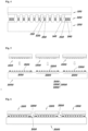
- FIG. 5 illustrates a state in which red, green, and blue micro-LED panels 1100, 1200, and 1300, a single CMOS backplane 2000 having CMOS cell areas 2100, 2200, and 2300 where the micro-LED panels 1100, 1200, and 1300 are to be electrically connected to CMOS cells, and bumps 3000 arranged on the CMOS cells to achieve full color in a micro-LED array display device according to one embodiment
- Fig. 6 illustrates a state in which the red, green, and blue micro-LED panels 1100, 1200, and 1300 are electrically connected to the single CMOS backplane 2000 through the bumps 3000.
- the micro-LED array display device capable of achieving full color includes a first micro-LED panel 1100, a second micro-LED panel 1200, and a third micro-LED panel 1300, each of which includes a plurality of arrayed micro-LED pixels.
- the first 1100, second 1200, and third micro-LED panels 1300 emit light of different wavelength bands.
- the first, second, and third micro-LED panels 1100, 1200, and 1300 may be constructed to emit red light, green light, and blue light, respectively.
- the micro-LED array display device capable of achieving full color includes a single CMOS backplane 2000 adapted to individually drive the micro-LED pixels of the first, second, and third micro-LED panels 1100, 1200, and 1300.
- the single CMOS backplane 2000 includes a plurality of CMOS cells corresponding to the micro-LED pixels of the first, second, and third micro-LED panels 1100, 1200, and 1300.
- CMOS cell areas 2100, 2200, and 2300 are formed in the CMOS backplane 2000 such that the micro-LED panels 1100, 1200, and 1300 are arranged on the CMOS backplane 2000.
- the CMOS cell areas 2100, 2200, and 2300 are formed corresponding to the micro-LED panels 1100, 1200, and 1300, respectively.
- the micro-LED panels 1100, 1200, and 1300 are flip-chip bonded to the CMOS cell areas 2100, 2200, and 2300, respectively.
- a plurality of CMOS cells corresponding to the micro-LED pixels of the micro-LED panels 1100, 1200, and 1300 are formed in the CMOS cell areas 2100, 2200, and 2300, respectively.
- the micro-LED panels 1100, 1200, and 1300 are flip-chip bonded to the single CMOS backplane 2000 to electrically connect the micro-LED pixels to the CMOS cells.
- the CMOS cells are electrically connected to the micro-LED pixels through bumps 3000.
- the flip-chip bonding of the micro-LED panels 1100, 1200, and 1300 to the single CMOS backplane 2000 is performed in the same manner as that of the micro-LED panel 100 to the CMOS backplane 200 explained with reference to Figs. 1 to 4 .
- Common cells are formed in the CMOS cell areas 2100, 2200, and 2300 on the single CMOS backplane 2000 and are electrically connected to first conductivity-type metal layers of the micro-LED panels 1100, 1200, and 1300 through common bumps.
- the micro-LED array display device in which the plurality of independently fabricated micro-LED panels emitting light of different wavelength bands, i.e. red, light, and blue light, are flip-chip bonded to the single CMOS backplane 2000 can focus three colors on the same area using an optical system to achieve full color, thus overcoming the technical difficulties of the prior art in forming red, green, and blue light emitting structures on one substrate in the fabrication of micro-LEDs.
- the micro-LED array display device can avoid the inconvenience or difficulty of wire bonding for connecting LED chips to various data lines, which run along the longitudinal and transverse axes and are responsible for the control of the LED chips.
- the micro-LED array display device can eliminate the need to dispose elements responsible for signal control in LED chips at positions away from the LED chips, contributing to a reduction in the overall size of the display device.
- Fig. 7 is a view for briefly explaining the driving of the micro-LED array display device illustrated in Fig. 5 to achieve full color.
- the micro-LED array display device is driven in response to control signals from a drive IC 700.
- the control signals from the drive IC 700 are transmitted to the micro-LED pixels by the CMOS cells (i.e. CMOS integrated circuits) formed in the CMOS backplane 2000.
- the control signals from the drive IC 700 may be analog or digital signals.
- the digital signals may also be pulse width modulation (PWM) signals.
Landscapes
- Engineering & Computer Science (AREA)
- Manufacturing & Machinery (AREA)
- Led Device Packages (AREA)
- Devices For Indicating Variable Information By Combining Individual Elements (AREA)
- Led Devices (AREA)
- Wire Bonding (AREA)
Description
- The present invention relates to micro-LED array display devices, and more specifically to micro-LED array display devices in which a plurality of micro-LED pixels are arrayed on one micro-LED panel by etching for the production of LED chips and the pixel-arrayed micro-LED panel is flip-chip bonded to a CMOS backplane through bumps so that the micro-LED pixels can be individually driven, thus being suitable for microdisplay applications.
- Demand for light emitting diodes (LEDs) has expanded exponentially in terms of low power consumption and environmental friendliness. LEDs are used as backlights for lighting apparatuses and LCD devices and are widely applied to display devices.
- LEDs are kinds of solid-state elements that convert electrical energy into light. LEDs are based on the principle that when a voltage is applied between two doped layers, i.e. an n-type semiconductor layer and a p-type semiconductor layer, between which an active layer is interposed, electrons and holes are injected into and recombine in the active layer to emit light. LEDs can be driven at relatively low voltage and have high energy efficiency. Due to these advantages, LEDs release a small amount of heat. LEDs can be produced in various types. Particularly, micro-LED array display devices are fabricated based on types of LEDs in which a plurality of micro-LED pixels are formed on one wafer. According to a conventional method for the fabrication of a micro-LED array display device in which a plurality of micro-LED pixels are formed on one wafer, a p-type terminal and an n-type terminal are formed in each pixel through a chip production process and are arrayed along the longitudinal and transverse axes of signal lines to drive the pixel. In this case, elements responsible for signal control in the micro-LED pixels should be disposed in the vicinity of the micro-LED pixels, resulting in an increase in the size of the micro-LED array display device. Further, data lines arrayed along the longitudinal and transverse axes should be connected to the micro-LED pixels by wire bonding, making the process complicated and inconvenient.
- The formation of a plurality of micro-LED pixels on one substrate technically limits the production of structures emitting red, green, and blue light. Because of this technical difficulty, the use of LEDs as light sources in micro-LED array display devices inevitably leads to the emission of monochromatic light. Thus, there is a need in the art for an approach that can provide a solution to the problems of the prior art.
WO 2015/095614 ,KR 20160027730 US 2015/254046 are examples of LED devices according to the prior art. - One object of the present invention is to provide a micro-LED array display device according to claim 1, wherein micro-LED pixels are flip-chip bonded to corresponding CMOS cells formed on a CMOS backplane through bumps, thus avoiding the complexity and inconvenience of wire bonding for connecting micro-LED pixels to various data lines while enabling individual control of the micro-LED pixels.
- A further object of the present invention is to provide a micro-LED array display device according to claim 4, wherein micro-LED panels, each including a plurality of micro-LED pixels, are flip-chip bonded to a single CMOS backplane, thus overcoming the difficulties of the prior art in forming red, green, and blue light emitting structures including micro-LED pixels formed on one substrate.
- According to the present invention, there is provided a micro-LED array display device including: a micro-LED panel including a plurality of micro-LED pixels; a CMOS backplane including a plurality of CMOS cells corresponding to the micro-LED pixels to individually drive the micro-LED pixels; and bumps electrically connecting the micro-LED pixels to the corresponding CMOS cells in a state in which the micro-LED pixels are arranged to face the CMOS cells, wherein the micro-LED pixels are flip-chip bonded to the corresponding CMOS cells formed on the CMOS backplane through the bumps so that the micro-LED pixels are individually controlled, wherin a first conductivity-type metal layer formed over a portion of the exposed portions of the first conductivity-type semiconductor layer, the first conductivity-type metal layer being spaced apart from the micro-LED pixels, wherein the first conductivity-type metal layer functions as a common electrode of the micro-LED pixels, wherein the first conductivity-type metal layer has the same height as the micro-LED pixels, wherein the first conductivity-type metal layer is formed along the periphery of the micro-LED panel on the first conductivity-type semiconductor layer.
- According to one embodiment, the micro-LED pixels are formed by growing a first conductivity-type semiconductor layer, an active layer, and a second conductivity-type semiconductor layer in this order on a substrate and etching the layers, the micro-LED pixels have a vertical structure including the first conductivity-type semiconductor layer, the active layer, and the second conductivity-type semiconductor layer formed in this order, and the active layer and the second conductivity-type semiconductor layer are removed from the exposed portions of the first conductivity-type semiconductor layer where none of the micro-LED pixels are formed.
- According to one embodiment, a first conductivity-type metal layer is formed over the portions of the first conductivity-type semiconductor layer where none of the micro-LED pixels are formed and is spaced apart from the micro-LED pixels.
- According to the present invention, the first conductivity-type metal layer is formed along the periphery of the micro-LED panel on the first conductivity-type semiconductor layer.
- According to the present invention, the first conductivity-type metal layer has the same height as the micro-LED pixels.
- According to one embodiment, the first conductivity-type metal layer functions as a common electrode of the micro-LED pixels.
- According to one embodiment, the CMOS backplane includes a common cell formed at a position corresponding to the first conductivity-type metal layer and the first conductivity-type metal layer is electrically connected to the common cell through a common bump.
- According to one embodiment, the first conductivity-type is n-type and the second conductivity-type is p-type.
- According to one embodiment, the substrate is made of a material selected from sapphire, SiC, Si, glass, and ZnO.
- According to one embodiment, the bumps are formed on the CMOS cells and are melted by heating such that the CMOS cells are electrically connected to the corresponding micro-LED pixels.
- According to an embodiment, there is provided a micro-LED array display device including: first, second, and third micro-LED panels emitting light of different wavelength bands, each of the micro-LED panels including a plurality of micro-LED pixels; a single CMOS backplane including a plurality of CMOS cells corresponding to the micro-LED pixels of the first, second, and third micro-LED panels to individually drive the micro-LED pixels; and bumps electrically connecting the micro-LED pixels of the first, second, and third micro-LED panels to the corresponding CMOS cells in a state in which the micro-LED pixels of the first, second, and third micro-LED panels are arranged to face the CMOS cells, wherein the micro-LED pixels of the first, second, and third micro-LED panels are flip-chip bonded to the corresponding CMOS cells formed on the CMOS backplane through the bumps so that the micro-LED pixels are individually controlled.
- In the new concept of micro-LED array display device according to an embodiment, micro-LED pixels are flip-chip bonded to micro-LED pixels formed on a CMOS backplane through bumps, avoiding the complexity and inconvenience of wire bonding for connecting micro-LED pixels to various data lines while enabling individual control of the micro-LED pixels. The micro-LED array display device of an embodiment in which a plurality of micro-LED panels emitting red, green, and blue light are flip-chip bonded to a single CMOS backplane through bumps can focus three colors on the same area using an optical system to achieve full color. Therefore, the micro-LED array display device of the embodiment is effective in overcoming the technical difficulties of the prior art in forming red, green, and blue light emitting structures including a plurality of micro-LED pixels on one substrate.
- These and/or other aspects and advantages of the invention will become apparent and more readily appreciated from the following description of the embodiments, taken in conjunction with the accompanying drawings of which:
-
Fig. 1 illustrates an exemplarymicro-LED panel 100 of a micro-LED array display device according to one embodiment; -
Fig. 2 illustrates themicro-LED panel 100 ofFig. 1 including micro-LED pixels and aCMOS backplane 200 including a plurality of CMOS cells adapted to individually drive the micro-LED pixels of themicro-LED panel 100; -
Fig. 3 illustrates a state in which themicro-LED panel 100 and theCMOS backplane 200 illustrated inFig. 2 are electrically connected to each other throughbumps 300 arranged on theCMOS backplane 200; -
Fig. 4 illustrates a state in which themicro-LED panel 100 and theCMOS backplane 200 illustrated inFig. 3 are arranged to face each other through thebumps 300 to electrically connect the micro-LED pixels of themicro-LED panel 100 to the CMOS cells of theCMOS backplane 200; -
Fig. 5 illustrates a state in which red, green, and bluemicro-LED panels single CMOS backplane 2000 havingCMOS cell areas micro-LED panels bumps 3000 arranged on the CMOS cells to achieve full color in a micro-LED array display device according to one embodiment; -
Fig. 6 illustrates a state in which the red, green, and bluemicro-LED panels single CMOS backplane 2000 through thebumps 3000 in the micro-LED array display device ofFig. 5 ; and -
Fig. 7 is a view for briefly explaining the driving of the micro-LED array display device illustrated inFig. 5 to achieve full color. - The present disclosure is directed to a micro-LED array display device in which micro-LED pixels are arrayed by MESA etching and are flip-chip bonded to a CMOS backplane, thus being applicable to a micro display, such as a head mounted display (HMD) or head up display (HUD). In the micro-LED array display device of the present disclosure, micro-LED pixels arrayed by MESA etching for the production of LED chips are flip-chip bonded to a CMOS backplane so that they can be individually driven. The present disclosure is also directed to a micro-LED array display device in which three red, green, and blue light emitting elements, i.e. micro-LED panels, are arrayed on a CMOS backplane to achieve full color.
- Preferred embodiments will now be described with reference to the accompanying drawings. The drawings and embodiments described with reference to the drawings are simplified and illustrated such that those skilled in the art can readily understand the present invention. Accordingly, the drawings and the embodiments should not be construed as limiting the scope of the present invention.
-
Fig. 1 illustrates an exemplarymicro-LED panel 100 of a micro-LED array display device according to one embodiment,Fig. 2 illustrates themicro-LED panel 100 including micro-LED pixels and aCMOS backplane 200 including a plurality of CMOS cells adapted to individually drive the micro-LED pixels of themicro-LED panel 100,Fig. 3 illustrates a state in which themicro-LED panel 100 and theCMOS backplane 200 are electrically connected to each other throughbumps 300 arranged on theCMOS backplane 200, andFig. 4 illustrates a state in which themicro-LED panel 100 and theCMOS backplane 200 are arranged to face each other through thebumps 300 to electrically connect the micro-LED pixels of themicro-LED panel 100 to the CMOS cells of theCMOS backplane 200. - Referring first to
Figs. 1 to 4 , a description will be given of a micro-LED array display device according to one embodiment. The micro-LED array display device includes amicro-LED panel 100, aCMOS backplane 200, andbumps 300. Themicro-LED panel 100 includes a plurality ofmicro-LED pixels 130. TheCMOS backplane 200 includes a plurality ofCMOS cells 230 corresponding to themicro-LED pixels 130 to individually drive themicro-LED pixels 130. Themicro-LED pixels 130 are electrically connected to thecorresponding CMOS cells 230 through thebumps 300 in a state in which themicro-LED pixels 130 are arranged to face theCMOS cells 230. InFigs. 1 to 4 , only one of the micro-LED pixels and only one of the CMOS cells are denoted byreference numerals micro-LED pixels 130 are flip-chip bonded to thecorresponding CMOS cells 230 formed on theCMOS backplane 200 through thebumps 300. Due to this construction, themicro-LED pixels 130 can be individually controlled. - The
micro-LED pixels 130 of themicro-LED panel 100 are formed by growing a first conductivity-type semiconductor layer 132, anactive layer 134, and a second conductivity-type semiconductor layer 136 in this order on asubstrate 110 and etching the layers. The micro-LED pixels have a vertical structure including the first conductivity-type semiconductor layer 132, theactive layer 134, and the second conductivity-type semiconductor layer 136 formed in this order on thesubstrate 110. Thesubstrate 110 may be made of a material selected from sapphire, SiC, Si, glass, and ZnO. The first conductivity-type semiconductor layer 132 may be an n-type semiconductor layer and the second conductivity-type semiconductor layer 136 may be a p-type semiconductor layer. Theactive layer 134 is a region where electrons from the first conductivity-type semiconductor layer 132 recombine with holes from the second conductivity-type semiconductor layer 136 when power is applied. - The second conductivity-
type semiconductor layer 136 and theactive layer 134 are removed from the etchedportions 120 of themicro-LED panel 100 where none of themicro-LED pixels 130 are formed, and as a result, the first conductivity-type semiconductor layer is exposed in the etched portions. Themicro-LED panel 100 includes a first conductivity-type metal layer 140 formed over theportions 120 of the first conductivity-type semiconductor layer 132 where none of themicro-LED pixels 130 are formed. The first conductivity-type metal layer 140 is spaced apart from themicro-LED pixels 130. According to the present invention, the first conductivity-type metal layer 140 is formed with a predetermined width along the periphery of themicro-LED panel 100 on the first conductivity-type semiconductor layer 132. According to the present invention, the first conductivity-type metal layer 140 has the same height as themicro-LED pixels 130. The first conductivity-type metal layer 140 is electrically connected to theCMOS backplane 200 through thebumps 300. As a result, the first conductivity-type metal layer 140 functions as a common electrode of themicro-LED pixels 130. For example, the first conductivity-type metal layer 140 may be a common ground. - The plurality of
CMOS cells 230 of theCMOS backplane 200 serve to individually drive themicro-LED pixels 130. TheCMOS cells 230 are electrically connected to the corresponding micro-LED pixels throughbumps 330. TheCMOS cells 230 are integrated circuits for individually driving the corresponding micro-LED pixels. TheCMOS backplane 200 may be, for example, an active matrix (AM) panel. Specifically, each of theCMOS cells 230 may be a pixel driving circuit including two transistors and one capacitor. When themicro-LED panel 100 is flip-chip bonded to theCMOS backplane 200 through thebumps 300, each of the micro-LED pixels may be arranged between a drain terminal and a common ground terminal (e.g., reference numeral 240) of a transistor of the pixel driving circuit to form an equivalent circuit. - The
CMOS backplane 200 includes acommon cell 240 formed at a position corresponding to the first conductivity-type metal layer 140. The first conductivity-type metal layer 140 is electrically connected to thecommon cell 240 through acommon bump 340. Herein, thebumps 300 is often intended to include thebumps 330 electrically connecting the plurality of CMOS cells to the micro-LED pixels and thecommon bump 340 electrically connecting the first conductivity-type metal layer 140 to thecommon cell 240. - As illustrated in
Fig. 3 , theCMOS backplane 200 on which theCMOS cells 230 are arranged faces themicro-LED panel 100. After theCMOS cells 230 are brought into contact with themicro-LED pixels 130 in a one-to-one relationship, thebumps 330 and thecommon bump 340 are melted by heating. As a result, theCMOS cells 230 are electrically connected to the correspondingmicro-LED pixels 130, as illustrated inFig. 4 . - Referring next to
Figs. 5 and 6 , a description will be given of a micro-LED array display device capable of achieving full color according to a further embodiment.Fig. 5 illustrates a state in which red, green, and bluemicro-LED panels single CMOS backplane 2000 havingCMOS cell areas micro-LED panels Fig. 6 illustrates a state in which the red, green, and bluemicro-LED panels single CMOS backplane 2000 through thebumps 3000. - Referring to these figures, the micro-LED array display device capable of achieving full color includes a first
micro-LED panel 1100, a secondmicro-LED panel 1200, and a thirdmicro-LED panel 1300, each of which includes a plurality of arrayed micro-LED pixels. The first 1100, second 1200, and thirdmicro-LED panels 1300 emit light of different wavelength bands. For example, the first, second, and thirdmicro-LED panels single CMOS backplane 2000 adapted to individually drive the micro-LED pixels of the first, second, and thirdmicro-LED panels single CMOS backplane 2000 includes a plurality of CMOS cells corresponding to the micro-LED pixels of the first, second, and thirdmicro-LED panels CMOS cell areas CMOS backplane 2000 such that themicro-LED panels CMOS backplane 2000. TheCMOS cell areas micro-LED panels micro-LED panels CMOS cell areas micro-LED panels CMOS cell areas micro-LED panels single CMOS backplane 2000 to electrically connect the micro-LED pixels to the CMOS cells. The CMOS cells are electrically connected to the micro-LED pixels throughbumps 3000. The flip-chip bonding of themicro-LED panels single CMOS backplane 2000 is performed in the same manner as that of themicro-LED panel 100 to theCMOS backplane 200 explained with reference toFigs. 1 to 4 . - Common cells are formed in the
CMOS cell areas single CMOS backplane 2000 and are electrically connected to first conductivity-type metal layers of themicro-LED panels - As described before, the micro-LED array display device in which the plurality of independently fabricated micro-LED panels emitting light of different wavelength bands, i.e. red, light, and blue light, are flip-chip bonded to the
single CMOS backplane 2000 can focus three colors on the same area using an optical system to achieve full color, thus overcoming the technical difficulties of the prior art in forming red, green, and blue light emitting structures on one substrate in the fabrication of micro-LEDs. In addition, the micro-LED array display device can avoid the inconvenience or difficulty of wire bonding for connecting LED chips to various data lines, which run along the longitudinal and transverse axes and are responsible for the control of the LED chips. Furthermore, the micro-LED array display device can eliminate the need to dispose elements responsible for signal control in LED chips at positions away from the LED chips, contributing to a reduction in the overall size of the display device. - Finally,
Fig. 7 is a view for briefly explaining the driving of the micro-LED array display device illustrated inFig. 5 to achieve full color. As illustrated inFig. 7 , the micro-LED array display device is driven in response to control signals from adrive IC 700. The control signals from thedrive IC 700 are transmitted to the micro-LED pixels by the CMOS cells (i.e. CMOS integrated circuits) formed in theCMOS backplane 2000. The control signals from thedrive IC 700 may be analog or digital signals. The digital signals may also be pulse width modulation (PWM) signals. -
- 100, 1100, 1200, 1300: Micro-LED panels
- 110: Substrate
- 120, 132: First conductivity-type semiconductor layers
- 130: Micro-LED pixel
- 134: Active layer
- 136: Second conductivity-type semiconductor layer
- 140: First conductivity-type metal layer
- 200, 2000: CMOS backplanes
- 230: CMOS cell
- 240: Common cell
- 340: Common bump
- 300, 330, 3000, 3100, 3200, 3300: Bumps
- 2100, 2200, 2300: CMOS cell areas
- 700: Drive IC
Claims (5)
- A micro-LED array display device including:a micro-LED panel(100) including a plurality of micro-LED pixels(130) formed on a substrate(110), the micro-LED pixels(130) have a vertical structure including a first conductivity-type semiconductor layer(132), an active layer(134), and a second conductivity-type semiconductor layer(136) in this order on the substrate(110), and the active layer(134) and the second conductivity-type semiconductor layer(136) are removed from exposed portions of the first conductivity-type semiconductor layer(132) where none of the micro-LED pixels(130) are formed;a CMOS backplane (200) including a plurality of CMOS cells (230) corresponding to the micro-LED pixels (130);bumps(330) electrically connecting the micro-LED pixels(130) to the corresponding CMOS cells(230) in a state in which the micro-LED pixels(130) are arranged to face the CMOS cells(230); andwherein the micro-LED pixels are flip-chip bonded to the corresponding CMOS cells formed on the CMOS backplane through the bumps so that the micro-LED pixels are individually controlled, characterized by comprisinga first conductivity-type metal layer(140) formed over a portion of the exposed portions of the first conductivity-type semiconductor layer(132), the first conductivity-type metal layer(140) being spaced apart from the micro-LED pixels(130), wherein the first conductivity-type metal layer(140) functions as a common electrode of the micro-LED pixels(130), wherein the first conductivity-type metal layer(140) has the same height as the micro-LED pixels(130), wherein the first conductivitytype metal layer(140) is formed along the periphery of the micro-LED panel(100) on the first conductivity-type semiconductor layer(132).
- The micro-LED array display device according to claim 1, wherein the CMOS backplane (200) comprises a common cell formed at a position corresponding to the first conductivity type metal layer (140) and the first conductivity-type metal layer (140) is electrically connected to the common cell through a common bump (330).
- The micro-LED array display device according to claim 1, wherein the substrate (110) is made of a material selected from sapphire, SiC, Si, glass, and ZnO.
- A micro-LED array display device to achieve full color including: a first (1100), a second (1200) and a third (1300) micro-LED panels emitting light of different wavelength bands each of the micro-LED panels (1100, 1200, 1300) including a plurality of micro-LED pixels (130) formed on a substrate (110), the micro-LED pixels (130) of each of the first (1100), second (1200) and third (1300) micro-LED panels have a vertical structure including a first conductivity-type semiconductor layer (132), an active layer (134), and a second conductivity-type semiconductor layer (136) formed in this order on the substrates (110) of the corresponding first (1100), second (1200) or third (1300) micro-LED panel, and the active layer(134) and the second conductivity-type semiconductor layer(136) are removed from exposed portions of the first conductivity-type semiconductor layer(132) where none of the micro-LED pixels(130) are formed, wherein a CMOS backplane (200) further includes a plurality of CMOS cells (230) corresponding to the micro-LED pixels (130) of the first (1100), second (1200) and third (1300) micro-LED panels, bumps (330) electrically connecting the micro-LED pixels (130) of first, second and third micro-LED panels to the corresponding CMOS cells (230) in a state in which the micro-LED pixels (130) of the first, "second and third micro-LED panels are arranged to face the CMOS cells; andwherein the micro-LED pixels (130) of the first (1100), second (1200) and third (1300) micro-LED panels are flip-chip bonded to the corresponding CMOS cells (230) formed on the CMOS backplane (200) through the bumps (330) so that the micro-LED pixels (130) are individually controlled, characterizing by the fact that a first conductivity-type metal layer (140) is further formed over a portion of the exposed portions of the first conductivity-type semiconductor layer (132) of each of the first, second and third micro-LED panels, the first conductivity-type metal layer (140) being spaced from the micro-LED pixels (130) of each of the first (1100), second (1200) and third (1300) micro-LED panels,wherein the first conductivity-type metal layer (110) functions as a common electrode of the micro-LED pixels (130), wherein the first conductivity-type metal layer(140) of each of the first (1100), second(1200) and third(1300) micro-LED panels has the same height as the micro-LED pixels(130) of each of the first (1100), second (1200) and third (1300) micro-LED panels, wherein the first conductivity-type metal layer(140) of each of the first (1100), second(1200) and third(1300) micro-LED panels is formed along the periphery of each of the first (1100), second(1200) and third(1300) micro-LED' panels on the first conductivity-type semiconductor layer(132).
- The micro-LED array display device according to claim 4, wherein the CMOS backplane (200) comprises a common cell formed at a position corresponding to the first conductivity-type metal layer (140) of each of the first (1100), second (1200) and third (1300) micro-LED panels and the first conductivity-type metal layer (140) is electrically connected to the common cell through a common bump.
Applications Claiming Priority (2)
| Application Number | Priority Date | Filing Date | Title |
|---|---|---|---|
| KR1020160090600A KR102617466B1 (en) | 2016-07-18 | 2016-07-18 | Micro led array display apparatus |
| PCT/KR2017/005354 WO2018016728A1 (en) | 2016-07-18 | 2017-05-23 | Micro led array display device |
Publications (4)
| Publication Number | Publication Date |
|---|---|
| EP3487266A1 EP3487266A1 (en) | 2019-05-22 |
| EP3487266A4 EP3487266A4 (en) | 2019-06-26 |
| EP3487266B1 true EP3487266B1 (en) | 2024-10-09 |
| EP3487266C0 EP3487266C0 (en) | 2024-10-09 |
Family
ID=58714722
Family Applications (1)
| Application Number | Title | Priority Date | Filing Date |
|---|---|---|---|
| EP17831202.1A Active EP3487266B1 (en) | 2016-07-18 | 2017-05-23 | Micro led array display device |
Country Status (7)
| Country | Link |
|---|---|
| US (3) | US10062675B2 (en) |
| EP (1) | EP3487266B1 (en) |
| JP (3) | JP6131374B1 (en) |
| KR (1) | KR102617466B1 (en) |
| CN (1) | CN109479354B (en) |
| TW (1) | TW201804608A (en) |
| WO (1) | WO2018016728A1 (en) |
Families Citing this family (90)
| Publication number | Priority date | Publication date | Assignee | Title |
|---|---|---|---|---|
| KR102617466B1 (en) * | 2016-07-18 | 2023-12-26 | 주식회사 루멘스 | Micro led array display apparatus |
| WO2018137139A1 (en) * | 2017-01-24 | 2018-08-02 | Goertek. Inc | Micro-led device, display apparatus and method for manufacturing a micro-led device |
| KR102305180B1 (en) * | 2017-04-25 | 2021-09-28 | 주식회사 루멘스 | Micro led display apparatus and method for fabricating the same |
| KR102399464B1 (en) * | 2017-06-27 | 2022-05-19 | 주식회사 루멘스 | LED panel |
| WO2019014036A1 (en) | 2017-07-11 | 2019-01-17 | Corning Incorporated | Tiled displays and methods of manufacturing the same |
| WO2019027820A1 (en) * | 2017-07-31 | 2019-02-07 | Yale University | Nanoporous micro-led devices and methods for making |
| CN111108613B (en) * | 2017-09-13 | 2024-01-16 | 夏普株式会社 | LED unit, image display element and manufacturing method thereof |
| WO2019083154A1 (en) * | 2017-10-26 | 2019-05-02 | 주식회사 루멘스 | Photography device comprising flash unit having individually controlled micro led pixels, and photography device for skin diagnosis |
| KR102456882B1 (en) * | 2017-11-24 | 2022-10-21 | 주식회사 루멘스 | method for making high efficiency micro LED module |
| US10989376B2 (en) * | 2017-11-28 | 2021-04-27 | Facebook Technologies, Llc | Assembling of strip of micro light emitting diodes onto backplane |
| EP3489998A1 (en) * | 2017-11-28 | 2019-05-29 | Facebook Technologies, LLC | Assembling of strip of micro light emitting diodes onto backplane |
| JP7079106B2 (en) * | 2018-01-24 | 2022-06-01 | シャープ株式会社 | Image display element and manufacturing method of image display element |
| KR101997104B1 (en) * | 2018-02-21 | 2019-07-05 | 순천대학교 산학협력단 | Micro array lighting emitting diode and method for manufacturing the same |
| KR102521582B1 (en) * | 2018-04-03 | 2023-04-12 | 삼성전자주식회사 | Light emitting diode display device |
| TWI672683B (en) * | 2018-04-03 | 2019-09-21 | 友達光電股份有限公司 | Display panel |
| US10652963B2 (en) | 2018-05-24 | 2020-05-12 | Lumiode, Inc. | LED display structures and fabrication of same |
| KR102757963B1 (en) | 2018-05-24 | 2025-01-22 | 다이니폰 인사츠 가부시키가이샤 | Sealing material sheet for self-luminous display or direct backlight, self-luminous display, direct backlight |
| JP7066537B2 (en) | 2018-06-06 | 2022-05-13 | 株式会社ジャパンディスプレイ | Display device and drive method of display device |
| JP7073198B2 (en) | 2018-06-07 | 2022-05-23 | 株式会社ジャパンディスプレイ | Display device |
| KR102033108B1 (en) * | 2018-07-06 | 2019-10-16 | 엘지전자 주식회사 | Display apparatus and driving method thereof |
| KR102587133B1 (en) | 2018-07-19 | 2023-10-10 | 삼성디스플레이 주식회사 | Display device |
| TWI661575B (en) | 2018-07-20 | 2019-06-01 | 錼創顯示科技股份有限公司 | Micro light emitting device and display apparatus |
| CN110739380B (en) * | 2018-07-20 | 2021-02-19 | 錼创显示科技股份有限公司 | Micro light-emitting element and display device |
| KR102603399B1 (en) | 2018-08-09 | 2023-11-17 | 삼성디스플레이 주식회사 | Display apparatus and manufacturing the same |
| JP7517989B2 (en) * | 2018-09-05 | 2024-07-17 | 株式会社半導体エネルギー研究所 | Display device, display module, and electronic device |
| JP7206321B2 (en) * | 2018-09-10 | 2023-01-17 | ルミレッズ ホールディング ベーフェー | Adaptive headlamp system for vehicles |
| US11091087B2 (en) | 2018-09-10 | 2021-08-17 | Lumileds Llc | Adaptive headlamp system for vehicles |
| KR102624297B1 (en) | 2018-10-02 | 2024-01-15 | 삼성디스플레이 주식회사 | Display device |
| CN111048543A (en) * | 2018-10-12 | 2020-04-21 | 致伸科技股份有限公司 | Display module |
| KR102732448B1 (en) * | 2018-11-27 | 2024-11-21 | 삼성전자주식회사 | Micro light source array, display device having the same and method of manufacturing display device |
| US11380252B2 (en) | 2018-12-21 | 2022-07-05 | Lumiode, Inc. | Addressing for emissive displays |
| US11640063B2 (en) * | 2018-12-28 | 2023-05-02 | Magic Leap, Inc. | Variable pixel density display system with mechanically-actuated image projector |
| WO2020142208A1 (en) * | 2019-01-02 | 2020-07-09 | Lumiode, Inc. | System and method of fabricating display structures |
| US11239399B2 (en) | 2019-02-05 | 2022-02-01 | Facebook Technologies, Llc | Architecture for hybrid TFT-based micro display projector |
| US11355665B2 (en) | 2019-06-19 | 2022-06-07 | Facebook Technologies, Llc | Process flow for hybrid TFT-based micro display projector |
| JP2022518352A (en) * | 2019-02-05 | 2022-03-15 | フェイスブック・テクノロジーズ・リミテッド・ライアビリティ・カンパニー | Process flow for hybrid TFT-based microdisplay projectors |
| JP2020134716A (en) | 2019-02-20 | 2020-08-31 | 株式会社ジャパンディスプレイ | Display |
| CN109888085B (en) * | 2019-03-11 | 2021-01-26 | 京东方科技集团股份有限公司 | Display panel and preparation method thereof |
| JP7289681B2 (en) * | 2019-03-20 | 2023-06-12 | 株式会社ジャパンディスプレイ | Display device |
| US11626448B2 (en) * | 2019-03-29 | 2023-04-11 | Lumileds Llc | Fan-out light-emitting diode (LED) device substrate with embedded backplane, lighting system and method of manufacture |
| CN109841710B (en) * | 2019-04-12 | 2020-05-15 | 南京大学 | GaN Micro-LED array device for transparent display and preparation method thereof |
| US11637219B2 (en) * | 2019-04-12 | 2023-04-25 | Google Llc | Monolithic integration of different light emitting structures on a same substrate |
| WO2020219039A1 (en) * | 2019-04-24 | 2020-10-29 | Hewlett-Packard Development Company, L.P. | Displays with pixels coupled by beam splitters |
| US11710760B2 (en) | 2019-06-21 | 2023-07-25 | Semiconductor Energy Laboratory Co., Ltd. | Display device, display module, electronic device, and manufacturing method of display device |
| JP2021012282A (en) | 2019-07-05 | 2021-02-04 | 株式会社ジャパンディスプレイ | Display |
| KR102814511B1 (en) * | 2019-09-04 | 2025-05-29 | 쑤저우 레킨 세미컨덕터 컴퍼니 리미티드 | Lighting emitting device package |
| TWI774130B (en) * | 2019-11-19 | 2022-08-11 | 美商亮銳公司 | Fan out structure for light-emitting diode (led) device and lighting system |
| US11156346B2 (en) | 2019-11-19 | 2021-10-26 | Lumileds Llc | Fan out structure for light-emitting diode (LED) device and lighting system |
| KR20220104165A (en) | 2019-11-21 | 2022-07-26 | 가부시키가이샤 한도오따이 에네루기 켄큐쇼 | A display device, a display module, an electronic device, and a manufacturing method of the display device |
| US11508700B2 (en) * | 2019-12-10 | 2022-11-22 | Meta Platforms Technologies, Llc | Left and right projectors for display device |
| KR102827179B1 (en) | 2019-12-23 | 2025-07-01 | 삼성디스플레이 주식회사 | Display apparatus and manufacturing method thereof |
| CN111063270B (en) * | 2019-12-30 | 2022-06-21 | 錼创显示科技股份有限公司 | Micro light-emitting element display device |
| US11664347B2 (en) | 2020-01-07 | 2023-05-30 | Lumileds Llc | Ceramic carrier and build up carrier for light-emitting diode (LED) array |
| KR102795496B1 (en) | 2020-01-09 | 2025-04-11 | 주식회사 엘지화학 | Micro led display |
| GB2593699B (en) | 2020-03-30 | 2022-10-26 | Plessey Semiconductors Ltd | Monolithic LED pixel |
| US12107072B2 (en) | 2020-04-06 | 2024-10-01 | Google Llc | Display backplane including an array of tiles |
| US12224304B2 (en) | 2020-04-09 | 2025-02-11 | Raysolve Optoelectronics (Suzhou) Company Limited | Light emitting diode structure with individual fuctionable LED units and method for manufacturing the same |
| KR102194978B1 (en) * | 2020-04-29 | 2020-12-24 | (주) 리가스텍 | Micro display device and method for manufacturing the same |
| WO2022019349A1 (en) * | 2020-07-21 | 2022-01-27 | 엘지전자 주식회사 | Transfer substrate used for manufacturing display device, display device, and method for manufacturing display device |
| US11830862B2 (en) | 2020-11-12 | 2023-11-28 | Excellence Opto. Inc. | Chip structure of micro light-emitting diode display |
| CN112669715B (en) * | 2020-12-24 | 2022-08-05 | 深圳市华星光电半导体显示技术有限公司 | Connecting piece, display panel, manufacturing method of display panel and display device |
| JP7581951B2 (en) * | 2021-02-23 | 2024-11-13 | 豊田合成株式会社 | Micro LED Display |
| US11489008B2 (en) | 2021-02-23 | 2022-11-01 | Toyoda Gosei Co., Ltd. | Light-emitting device |
| US12191340B2 (en) | 2021-04-30 | 2025-01-07 | Samsung Display Co., Ltd. | Display device |
| US12532591B2 (en) | 2021-04-30 | 2026-01-20 | Samsung Display Co., Ltd. | Display device having partition wall structure that finely divides wavelength conversion portions |
| KR20230033080A (en) | 2021-08-26 | 2023-03-08 | 삼성디스플레이 주식회사 | Display device and manufacturing method of the same |
| US12336357B2 (en) | 2021-11-24 | 2025-06-17 | Meta Platforms Technologies, Llc | Alignment-free micro-display architecture |
| KR20240125558A (en) * | 2021-12-14 | 2024-08-19 | 소니 세미컨덕터 솔루션즈 가부시키가이샤 | Light-emitting devices and electronic devices |
| JP2023088865A (en) * | 2021-12-15 | 2023-06-27 | 豊田合成株式会社 | LED display |
| CN114334923B (en) * | 2021-12-23 | 2026-03-17 | 厦门士兰明镓化合物半导体有限公司 | Display screen, Micro-LED display substrate and its fabrication method |
| KR102940973B1 (en) | 2022-01-06 | 2026-03-18 | 삼성디스플레이 주식회사 | Display device and method for fabricating the same |
| KR102579242B1 (en) | 2022-02-22 | 2023-09-18 | 한국에너지공과대학교 | Micro LED display apparatus and method for fabricating the same |
| CN114627773B (en) * | 2022-03-11 | 2024-02-20 | 武汉华星光电半导体显示技术有限公司 | Spliced display panel |
| US12148361B2 (en) * | 2022-06-15 | 2024-11-19 | Lumileds Llc | Vehicular sparse led array |
| US12424600B1 (en) | 2022-11-07 | 2025-09-23 | Meta Platforms Technologies, Llc | Tiled display system for field of view expansion |
| KR102712126B1 (en) | 2023-02-21 | 2024-09-30 | 웨이브로드 주식회사 | Method for manufacturing microdisplay panel |
| KR102669057B1 (en) | 2023-02-07 | 2024-05-24 | 웨이브로드 주식회사 | Method for manufacturing microdisplay panel with reflector applied |
| KR102669051B1 (en) | 2023-02-21 | 2024-05-24 | 웨이브로드 주식회사 | Method for manufacturing vertical stacked microdisplay panel |
| WO2024167247A1 (en) * | 2023-02-07 | 2024-08-15 | 웨이브로드 주식회사 | Method for manufacturing microdisplay panel |
| KR102607680B1 (en) | 2023-02-07 | 2023-11-29 | 웨이브로드 주식회사 | Method for manufacturing microdisplay panel |
| KR102668094B1 (en) | 2023-03-13 | 2024-05-22 | 웨이브로드 주식회사 | Vertical stacked microdisplay panel without color filter and manufacturing method thereof |
| KR102862338B1 (en) * | 2023-08-10 | 2025-10-17 | 주식회사 글로벌테크놀로지 | Driving package having display and its manufacturing method |
| US12159566B1 (en) | 2023-10-23 | 2024-12-03 | Tectus Corporation | Backplane for multi-panel ultra-dense micro-LED display |
| KR102935285B1 (en) | 2024-01-22 | 2026-03-10 | 웨이브로드 주식회사 | Vertical stacked microdisplay panel |
| US20260040750A1 (en) * | 2024-07-31 | 2026-02-05 | Adeia Semiconductor Bonding Technologies Inc. | Efficient assembly for led displays |
| EP4739044A1 (en) | 2024-10-30 | 2026-05-06 | Wavelord Co., Ltd | Vertically stacked red-green-blue full-color chip-on-carrier for microled display panels and method of manufacturing the same |
| KR102849442B1 (en) | 2024-12-27 | 2025-08-22 | 웨이브로드 주식회사 | Microdisplay panel and manufacturing method thereof |
| KR102915393B1 (en) | 2025-01-06 | 2026-01-20 | 웨이브로드 주식회사 | Microdisplay panel and manufacturing method thereof |
| KR102915400B1 (en) | 2025-01-07 | 2026-01-20 | 웨이브로드 주식회사 | Microdisplay panel and manufacturing method thereof |
| KR102915403B1 (en) | 2025-01-10 | 2026-01-20 | 웨이브로드 주식회사 | Microdisplay panel and manufacturing method thereof |
Family Cites Families (40)
| Publication number | Priority date | Publication date | Assignee | Title |
|---|---|---|---|---|
| JPS537278B2 (en) * | 1973-07-17 | 1978-03-16 | ||
| JP3195720B2 (en) * | 1994-12-20 | 2001-08-06 | シャープ株式会社 | Multicolor LED element, LED display device using the multicolor LED element, and method of manufacturing multicolor LED element |
| JP3976812B2 (en) * | 1995-03-09 | 2007-09-19 | セイコーエプソン株式会社 | Polarized illumination device and projection display device |
| US5621225A (en) * | 1996-01-18 | 1997-04-15 | Motorola | Light emitting diode display package |
| JP2001044502A (en) * | 1999-07-28 | 2001-02-16 | Matsushita Electronics Industry Corp | Composite light emitting element and manufacture thereof |
| US6486499B1 (en) * | 1999-12-22 | 2002-11-26 | Lumileds Lighting U.S., Llc | III-nitride light-emitting device with increased light generating capability |
| JP2001326388A (en) * | 2000-05-12 | 2001-11-22 | Rohm Co Ltd | Semiconductor light emitting device |
| JP2001343706A (en) * | 2000-05-31 | 2001-12-14 | Sony Corp | Video display device |
| JP3906653B2 (en) * | 2000-07-18 | 2007-04-18 | ソニー株式会社 | Image display device and manufacturing method thereof |
| KR100470904B1 (en) | 2002-07-20 | 2005-03-10 | 주식회사 비첼 | High brightness nitride micro size light emitting diode and method of manufacturing the same |
| JP2004055944A (en) * | 2002-07-23 | 2004-02-19 | Matsushita Electric Ind Co Ltd | Method for manufacturing semiconductor light emitting device |
| JP2004079972A (en) * | 2002-08-22 | 2004-03-11 | Fuji Photo Film Co Ltd | Surface-emitting light emitting device |
| JP2005079385A (en) * | 2003-09-01 | 2005-03-24 | Toshiba Corp | Optical semiconductor device and optical signal input / output device |
| US7285801B2 (en) * | 2004-04-02 | 2007-10-23 | Lumination, Llc | LED with series-connected monolithically integrated mesas |
| JP2006012916A (en) * | 2004-06-22 | 2006-01-12 | Toyoda Gosei Co Ltd | Light emitting device |
| JP2006073618A (en) * | 2004-08-31 | 2006-03-16 | Toyoda Gosei Co Ltd | Optical element and manufacturing method thereof |
| JP2007324583A (en) * | 2006-05-01 | 2007-12-13 | Mitsubishi Chemicals Corp | Integrated semiconductor light emitting device and method of manufacturing the same |
| JP2010192802A (en) * | 2009-02-20 | 2010-09-02 | Sony Corp | Mounting board and display apparatus |
| WO2011008747A2 (en) | 2009-07-15 | 2011-01-20 | Cardiac Pacemakers, Inc. | Remote sensing in an implantable medical device |
| JP2011113989A (en) * | 2009-11-24 | 2011-06-09 | Oki Data Corp | Display panel and projection type display device |
| US8642363B2 (en) * | 2009-12-09 | 2014-02-04 | Nano And Advanced Materials Institute Limited | Monolithic full-color LED micro-display on an active matrix panel manufactured using flip-chip technology |
| US8557616B2 (en) * | 2009-12-09 | 2013-10-15 | Nano And Advanced Materials Institute Limited | Method for manufacturing a monolithic LED micro-display on an active matrix panel using flip-chip technology and display apparatus having the monolithic LED micro-display |
| KR101666442B1 (en) * | 2010-03-25 | 2016-10-17 | 엘지이노텍 주식회사 | Light emitting diode and Light emitting device comprising the same |
| KR101150861B1 (en) | 2010-08-16 | 2012-06-13 | 한국광기술원 | Light emitting diode having multi-cell structure and its manufacturing method |
| JP6095686B2 (en) * | 2011-12-06 | 2017-03-15 | オステンド・テクノロジーズ・インコーポレーテッド | Spatial optical type and spatio-temporal optical type directional light modulator |
| DE102011056888A1 (en) * | 2011-12-22 | 2013-06-27 | Osram Opto Semiconductors Gmbh | Display device and method for producing a display device |
| JP2013179215A (en) * | 2012-02-29 | 2013-09-09 | Toyohashi Univ Of Technology | Led array and photoelectric integrated device |
| DE102012217957B4 (en) * | 2012-10-01 | 2014-10-09 | Fraunhofer-Gesellschaft zur Förderung der angewandten Forschung e.V. | Method for producing a micro-LED matrix |
| US9159700B2 (en) * | 2012-12-10 | 2015-10-13 | LuxVue Technology Corporation | Active matrix emissive micro LED display |
| CN103456729B (en) * | 2013-07-26 | 2016-09-21 | 利亚德光电股份有限公司 | Light emitting diode (LED) display screen |
| EP3084338A4 (en) * | 2013-12-18 | 2017-07-26 | Leupold & Stevens, Inc. | Micro-pixelated led reticle display for optical aiming devices |
| US9207904B2 (en) * | 2013-12-31 | 2015-12-08 | Ultravision Technologies, Llc | Multi-panel display with hot swappable display panels and methods of servicing thereof |
| US9831387B2 (en) * | 2014-06-14 | 2017-11-28 | Hiphoton Co., Ltd. | Light engine array |
| FR3023065B1 (en) * | 2014-06-27 | 2017-12-15 | Commissariat Energie Atomique | P-N JUNCTION OPTOELECTRONIC DEVICE FOR IONIZATION OF FIELD EFFECT DOPANTS |
| KR20160027730A (en) * | 2014-09-02 | 2016-03-10 | 서울바이오시스 주식회사 | Light emitting diode |
| GB201420452D0 (en) * | 2014-11-18 | 2014-12-31 | Mled Ltd | Integrated colour led micro-display |
| KR102617466B1 (en) * | 2016-07-18 | 2023-12-26 | 주식회사 루멘스 | Micro led array display apparatus |
| CN110100309A (en) * | 2016-12-23 | 2019-08-06 | 株式会社流明斯 | Miniature LED module and its manufacturing method |
| JP6366799B1 (en) * | 2017-02-10 | 2018-08-01 | ルーメンス カンパニー リミテッド | Micro LED module and manufacturing method thereof |
| KR102399464B1 (en) * | 2017-06-27 | 2022-05-19 | 주식회사 루멘스 | LED panel |
-
2016
- 2016-07-18 KR KR1020160090600A patent/KR102617466B1/en active Active
- 2016-09-23 JP JP2016185382A patent/JP6131374B1/en active Active
-
2017
- 2017-04-17 JP JP2017081498A patent/JP6445075B2/en active Active
- 2017-05-23 CN CN201780042188.8A patent/CN109479354B/en active Active
- 2017-05-23 WO PCT/KR2017/005354 patent/WO2018016728A1/en not_active Ceased
- 2017-05-23 EP EP17831202.1A patent/EP3487266B1/en active Active
- 2017-05-31 TW TW106117896A patent/TW201804608A/en unknown
- 2017-06-04 US US15/613,233 patent/US10062675B2/en active Active
-
2018
- 2018-07-26 US US16/046,161 patent/US10784241B2/en active Active
- 2018-07-26 US US16/046,176 patent/US10607973B2/en active Active
- 2018-11-28 JP JP2018222671A patent/JP6722262B2/en active Active
Also Published As
| Publication number | Publication date |
|---|---|
| EP3487266A1 (en) | 2019-05-22 |
| US10607973B2 (en) | 2020-03-31 |
| JP2019068082A (en) | 2019-04-25 |
| KR20180009116A (en) | 2018-01-26 |
| US20180331086A1 (en) | 2018-11-15 |
| US10062675B2 (en) | 2018-08-28 |
| TW201804608A (en) | 2018-02-01 |
| JP6722262B2 (en) | 2020-07-15 |
| JP6445075B2 (en) | 2018-12-26 |
| CN109479354A (en) | 2019-03-15 |
| JP6131374B1 (en) | 2017-05-17 |
| KR102617466B1 (en) | 2023-12-26 |
| WO2018016728A1 (en) | 2018-01-25 |
| US20180019233A1 (en) | 2018-01-18 |
| EP3487266A4 (en) | 2019-06-26 |
| JP2018014481A (en) | 2018-01-25 |
| CN109479354B (en) | 2021-05-14 |
| US10784241B2 (en) | 2020-09-22 |
| US20180331085A1 (en) | 2018-11-15 |
| EP3487266C0 (en) | 2024-10-09 |
| JP2018014475A (en) | 2018-01-25 |
Similar Documents
| Publication | Publication Date | Title |
|---|---|---|
| US10607973B2 (en) | Micro-LED array display devices with CMOS cells | |
| JP7387699B2 (en) | display device | |
| US11985856B2 (en) | Display apparatus | |
| US11575067B2 (en) | Display substrate, display apparatus, and manufacturing method for display substrate | |
| TWI689092B (en) | Micro led display module having light transmissive substrate and manufacturing method thereof | |
| TW201732770A (en) | Semiconductor device having integrated thin film transistor circuit | |
| US20120223875A1 (en) | Monolithic full-color led micro-display on an active matrix panel manufactured using flip-chip technology | |
| KR102078643B1 (en) | Display appartus using one chip type led and fabrication method of the same | |
| TWI611573B (en) | Method for manufacturing micro light emitting diode display module | |
| TWI627740B (en) | Micro light emitting diode display module and manufacturing method thereof | |
| CN109037263A (en) | Micro- light-emitting diode display module and its manufacturing method with light-transmitting substrate | |
| CN109037262A (en) | The manufacturing method of micro- light-emitting diode display module | |
| TWI633681B (en) | Method for manufacturing micro light emitting diode display module | |
| CN109037260A (en) | Micro- light-emitting diode display module and its manufacturing method | |
| CN109037261A (en) | The manufacturing method of micro- light-emitting diode display module |
Legal Events
| Date | Code | Title | Description |
|---|---|---|---|
| STAA | Information on the status of an ep patent application or granted ep patent |
Free format text: STATUS: THE INTERNATIONAL PUBLICATION HAS BEEN MADE |
|
| PUAI | Public reference made under article 153(3) epc to a published international application that has entered the european phase |
Free format text: ORIGINAL CODE: 0009012 |
|
| STAA | Information on the status of an ep patent application or granted ep patent |
Free format text: STATUS: REQUEST FOR EXAMINATION WAS MADE |
|
| 17P | Request for examination filed |
Effective date: 20190107 |
|
| AK | Designated contracting states |
Kind code of ref document: A1 Designated state(s): AL AT BE BG CH CY CZ DE DK EE ES FI FR GB GR HR HU IE IS IT LI LT LU LV MC MK MT NL NO PL PT RO RS SE SI SK SM TR |
|
| AX | Request for extension of the european patent |
Extension state: BA ME |
|
| A4 | Supplementary search report drawn up and despatched |
Effective date: 20190528 |
|
| RIC1 | Information provided on ipc code assigned before grant |
Ipc: H01L 33/62 20100101ALI20190522BHEP Ipc: H01L 25/16 20060101AFI20190522BHEP |
|
| DAV | Request for validation of the european patent (deleted) | ||
| DAX | Request for extension of the european patent (deleted) | ||
| STAA | Information on the status of an ep patent application or granted ep patent |
Free format text: STATUS: EXAMINATION IS IN PROGRESS |
|
| 17Q | First examination report despatched |
Effective date: 20210421 |
|
| GRAP | Despatch of communication of intention to grant a patent |
Free format text: ORIGINAL CODE: EPIDOSNIGR1 |
|
| STAA | Information on the status of an ep patent application or granted ep patent |
Free format text: STATUS: GRANT OF PATENT IS INTENDED |
|
| INTG | Intention to grant announced |
Effective date: 20240702 |
|
| GRAS | Grant fee paid |
Free format text: ORIGINAL CODE: EPIDOSNIGR3 |
|
| GRAA | (expected) grant |
Free format text: ORIGINAL CODE: 0009210 |
|
| STAA | Information on the status of an ep patent application or granted ep patent |
Free format text: STATUS: THE PATENT HAS BEEN GRANTED |
|
| AK | Designated contracting states |
Kind code of ref document: B1 Designated state(s): AL AT BE BG CH CY CZ DE DK EE ES FI FR GB GR HR HU IE IS IT LI LT LU LV MC MK MT NL NO PL PT RO RS SE SI SK SM TR |
|
| REG | Reference to a national code |
Ref country code: CH Ref legal event code: EP |
|
| REG | Reference to a national code |
Ref country code: DE Ref legal event code: R096 Ref document number: 602017085405 Country of ref document: DE |
|
| REG | Reference to a national code |
Ref country code: IE Ref legal event code: FG4D |
|
| U01 | Request for unitary effect filed |
Effective date: 20241022 |
|
| U07 | Unitary effect registered |
Designated state(s): AT BE BG DE DK EE FI FR IT LT LU LV MT NL PT RO SE SI Effective date: 20241105 |
|
| PG25 | Lapsed in a contracting state [announced via postgrant information from national office to epo] |
Ref country code: HR Free format text: LAPSE BECAUSE OF FAILURE TO SUBMIT A TRANSLATION OF THE DESCRIPTION OR TO PAY THE FEE WITHIN THE PRESCRIBED TIME-LIMIT Effective date: 20241009 Ref country code: IS Free format text: LAPSE BECAUSE OF FAILURE TO SUBMIT A TRANSLATION OF THE DESCRIPTION OR TO PAY THE FEE WITHIN THE PRESCRIBED TIME-LIMIT Effective date: 20250209 |
|
| PG25 | Lapsed in a contracting state [announced via postgrant information from national office to epo] |
Ref country code: ES Free format text: LAPSE BECAUSE OF FAILURE TO SUBMIT A TRANSLATION OF THE DESCRIPTION OR TO PAY THE FEE WITHIN THE PRESCRIBED TIME-LIMIT Effective date: 20241009 |
|
| PG25 | Lapsed in a contracting state [announced via postgrant information from national office to epo] |
Ref country code: NO Free format text: LAPSE BECAUSE OF FAILURE TO SUBMIT A TRANSLATION OF THE DESCRIPTION OR TO PAY THE FEE WITHIN THE PRESCRIBED TIME-LIMIT Effective date: 20250109 |
|
| PG25 | Lapsed in a contracting state [announced via postgrant information from national office to epo] |
Ref country code: GR Free format text: LAPSE BECAUSE OF FAILURE TO SUBMIT A TRANSLATION OF THE DESCRIPTION OR TO PAY THE FEE WITHIN THE PRESCRIBED TIME-LIMIT Effective date: 20250110 |
|
| PG25 | Lapsed in a contracting state [announced via postgrant information from national office to epo] |
Ref country code: PL Free format text: LAPSE BECAUSE OF FAILURE TO SUBMIT A TRANSLATION OF THE DESCRIPTION OR TO PAY THE FEE WITHIN THE PRESCRIBED TIME-LIMIT Effective date: 20241009 |
|
| PG25 | Lapsed in a contracting state [announced via postgrant information from national office to epo] |
Ref country code: RS Free format text: LAPSE BECAUSE OF FAILURE TO SUBMIT A TRANSLATION OF THE DESCRIPTION OR TO PAY THE FEE WITHIN THE PRESCRIBED TIME-LIMIT Effective date: 20250109 |
|
| U20 | Renewal fee for the european patent with unitary effect paid |
Year of fee payment: 9 Effective date: 20250407 |
|
| PG25 | Lapsed in a contracting state [announced via postgrant information from national office to epo] |
Ref country code: SM Free format text: LAPSE BECAUSE OF FAILURE TO SUBMIT A TRANSLATION OF THE DESCRIPTION OR TO PAY THE FEE WITHIN THE PRESCRIBED TIME-LIMIT Effective date: 20241009 |
|
| PG25 | Lapsed in a contracting state [announced via postgrant information from national office to epo] |
Ref country code: SK Free format text: LAPSE BECAUSE OF FAILURE TO SUBMIT A TRANSLATION OF THE DESCRIPTION OR TO PAY THE FEE WITHIN THE PRESCRIBED TIME-LIMIT Effective date: 20241009 |
|
| PG25 | Lapsed in a contracting state [announced via postgrant information from national office to epo] |
Ref country code: CZ Free format text: LAPSE BECAUSE OF FAILURE TO SUBMIT A TRANSLATION OF THE DESCRIPTION OR TO PAY THE FEE WITHIN THE PRESCRIBED TIME-LIMIT Effective date: 20241009 |
|
| PLBE | No opposition filed within time limit |
Free format text: ORIGINAL CODE: 0009261 |
|
| STAA | Information on the status of an ep patent application or granted ep patent |
Free format text: STATUS: NO OPPOSITION FILED WITHIN TIME LIMIT |
|
| 26N | No opposition filed |
Effective date: 20250710 |
|
| REG | Reference to a national code |
Ref country code: CH Ref legal event code: H13 Free format text: ST27 STATUS EVENT CODE: U-0-0-H10-H13 (AS PROVIDED BY THE NATIONAL OFFICE) Effective date: 20251223 |
|
| PG25 | Lapsed in a contracting state [announced via postgrant information from national office to epo] |
Ref country code: CH Free format text: LAPSE BECAUSE OF NON-PAYMENT OF DUE FEES Effective date: 20250531 |
|
| GBPC | Gb: european patent ceased through non-payment of renewal fee |
Effective date: 20250523 |
|
| PG25 | Lapsed in a contracting state [announced via postgrant information from national office to epo] |
Ref country code: MC Free format text: LAPSE BECAUSE OF FAILURE TO SUBMIT A TRANSLATION OF THE DESCRIPTION OR TO PAY THE FEE WITHIN THE PRESCRIBED TIME-LIMIT Effective date: 20241009 |
|
| PG25 | Lapsed in a contracting state [announced via postgrant information from national office to epo] |
Ref country code: GB Free format text: LAPSE BECAUSE OF NON-PAYMENT OF DUE FEES Effective date: 20250523 |
|
| PG25 | Lapsed in a contracting state [announced via postgrant information from national office to epo] |
Ref country code: IE Free format text: LAPSE BECAUSE OF NON-PAYMENT OF DUE FEES Effective date: 20250523 |