KR20220104165A - A display device, a display module, an electronic device, and a manufacturing method of the display device - Google Patents
A display device, a display module, an electronic device, and a manufacturing method of the display device Download PDFInfo
- Publication number
- KR20220104165A KR20220104165A KR1020227016538A KR20227016538A KR20220104165A KR 20220104165 A KR20220104165 A KR 20220104165A KR 1020227016538 A KR1020227016538 A KR 1020227016538A KR 20227016538 A KR20227016538 A KR 20227016538A KR 20220104165 A KR20220104165 A KR 20220104165A
- Authority
- KR
- South Korea
- Prior art keywords
- insulating layer
- layer
- light emitting
- insulator
- oxide
- Prior art date
Links
- 238000004519 manufacturing process Methods 0.000 title claims description 39
- 239000010410 layer Substances 0.000 claims description 706
- 239000004065 semiconductor Substances 0.000 claims description 144
- 239000000758 substrate Substances 0.000 claims description 103
- 229910044991 metal oxide Inorganic materials 0.000 claims description 75
- 150000004706 metal oxides Chemical class 0.000 claims description 75
- 238000000034 method Methods 0.000 claims description 73
- 230000015572 biosynthetic process Effects 0.000 claims description 57
- VYPSYNLAJGMNEJ-UHFFFAOYSA-N Silicium dioxide Chemical compound O=[Si]=O VYPSYNLAJGMNEJ-UHFFFAOYSA-N 0.000 claims description 31
- 238000006243 chemical reaction Methods 0.000 claims description 31
- XUIMIQQOPSSXEZ-UHFFFAOYSA-N Silicon Chemical compound [Si] XUIMIQQOPSSXEZ-UHFFFAOYSA-N 0.000 claims description 29
- 229910052710 silicon Inorganic materials 0.000 claims description 29
- 239000010703 silicon Substances 0.000 claims description 29
- 229910052814 silicon oxide Inorganic materials 0.000 claims description 27
- 229910052581 Si3N4 Inorganic materials 0.000 claims description 26
- HQVNEWCFYHHQES-UHFFFAOYSA-N silicon nitride Chemical compound N12[Si]34N5[Si]62N3[Si]51N64 HQVNEWCFYHHQES-UHFFFAOYSA-N 0.000 claims description 26
- 150000001875 compounds Chemical class 0.000 claims description 23
- 230000003287 optical effect Effects 0.000 claims description 23
- TWNQGVIAIRXVLR-UHFFFAOYSA-N oxo(oxoalumanyloxy)alumane Chemical compound O=[Al]O[Al]=O TWNQGVIAIRXVLR-UHFFFAOYSA-N 0.000 claims description 22
- 238000004040 coloring Methods 0.000 claims description 15
- 229910000449 hafnium oxide Inorganic materials 0.000 claims description 14
- WIHZLLGSGQNAGK-UHFFFAOYSA-N hafnium(4+);oxygen(2-) Chemical compound [O-2].[O-2].[Hf+4] WIHZLLGSGQNAGK-UHFFFAOYSA-N 0.000 claims description 14
- 238000012545 processing Methods 0.000 claims description 9
- 239000002346 layers by function Substances 0.000 claims description 8
- 229910052696 pnictogen Inorganic materials 0.000 claims description 8
- 230000008569 process Effects 0.000 claims description 8
- 229910052795 boron group element Inorganic materials 0.000 claims description 7
- 239000011159 matrix material Substances 0.000 claims description 6
- JMASRVWKEDWRBT-UHFFFAOYSA-N Gallium nitride Chemical compound [Ga]#N JMASRVWKEDWRBT-UHFFFAOYSA-N 0.000 claims description 5
- 229910002601 GaN Inorganic materials 0.000 claims description 3
- 239000012212 insulator Substances 0.000 description 278
- 239000004020 conductor Substances 0.000 description 181
- 239000010408 film Substances 0.000 description 160
- 230000006870 function Effects 0.000 description 107
- 229910052760 oxygen Inorganic materials 0.000 description 52
- QVGXLLKOCUKJST-UHFFFAOYSA-N atomic oxygen Chemical compound [O] QVGXLLKOCUKJST-UHFFFAOYSA-N 0.000 description 50
- 239000001301 oxygen Substances 0.000 description 50
- 239000001257 hydrogen Substances 0.000 description 39
- 229910052739 hydrogen Inorganic materials 0.000 description 39
- UFHFLCQGNIYNRP-UHFFFAOYSA-N Hydrogen Chemical compound [H][H] UFHFLCQGNIYNRP-UHFFFAOYSA-N 0.000 description 35
- 239000013078 crystal Substances 0.000 description 35
- 239000000463 material Substances 0.000 description 31
- 239000011701 zinc Substances 0.000 description 30
- 239000012535 impurity Substances 0.000 description 28
- 238000009792 diffusion process Methods 0.000 description 24
- 230000001965 increasing effect Effects 0.000 description 20
- 229910052782 aluminium Inorganic materials 0.000 description 18
- XAGFODPZIPBFFR-UHFFFAOYSA-N aluminium Chemical compound [Al] XAGFODPZIPBFFR-UHFFFAOYSA-N 0.000 description 18
- 239000002096 quantum dot Substances 0.000 description 18
- 230000004888 barrier function Effects 0.000 description 17
- PXHVJJICTQNCMI-UHFFFAOYSA-N Nickel Chemical compound [Ni] PXHVJJICTQNCMI-UHFFFAOYSA-N 0.000 description 16
- 229910052738 indium Inorganic materials 0.000 description 16
- IJGRMHOSHXDMSA-UHFFFAOYSA-N Atomic nitrogen Chemical compound N#N IJGRMHOSHXDMSA-UHFFFAOYSA-N 0.000 description 14
- RTAQQCXQSZGOHL-UHFFFAOYSA-N Titanium Chemical compound [Ti] RTAQQCXQSZGOHL-UHFFFAOYSA-N 0.000 description 13
- 238000004891 communication Methods 0.000 description 13
- 229910052733 gallium Inorganic materials 0.000 description 13
- APFVFJFRJDLVQX-UHFFFAOYSA-N indium atom Chemical compound [In] APFVFJFRJDLVQX-UHFFFAOYSA-N 0.000 description 13
- 239000000203 mixture Substances 0.000 description 13
- 229910052719 titanium Inorganic materials 0.000 description 13
- 239000010936 titanium Substances 0.000 description 13
- 229910052751 metal Inorganic materials 0.000 description 12
- RYGMFSIKBFXOCR-UHFFFAOYSA-N Copper Chemical compound [Cu] RYGMFSIKBFXOCR-UHFFFAOYSA-N 0.000 description 11
- GYHNNYVSQQEPJS-UHFFFAOYSA-N Gallium Chemical compound [Ga] GYHNNYVSQQEPJS-UHFFFAOYSA-N 0.000 description 11
- 229910052715 tantalum Inorganic materials 0.000 description 11
- GUVRBAGPIYLISA-UHFFFAOYSA-N tantalum atom Chemical compound [Ta] GUVRBAGPIYLISA-UHFFFAOYSA-N 0.000 description 11
- WFKWXMTUELFFGS-UHFFFAOYSA-N tungsten Chemical compound [W] WFKWXMTUELFFGS-UHFFFAOYSA-N 0.000 description 11
- 229910052721 tungsten Inorganic materials 0.000 description 11
- 239000010937 tungsten Substances 0.000 description 11
- XLYOFNOQVPJJNP-UHFFFAOYSA-N water Substances O XLYOFNOQVPJJNP-UHFFFAOYSA-N 0.000 description 11
- 229910052725 zinc Inorganic materials 0.000 description 11
- 238000002441 X-ray diffraction Methods 0.000 description 10
- XLOMVQKBTHCTTD-UHFFFAOYSA-N Zinc monoxide Chemical compound [Zn]=O XLOMVQKBTHCTTD-UHFFFAOYSA-N 0.000 description 10
- HCHKCACWOHOZIP-UHFFFAOYSA-N Zinc Chemical compound [Zn] HCHKCACWOHOZIP-UHFFFAOYSA-N 0.000 description 9
- 239000010949 copper Substances 0.000 description 9
- 229910052735 hafnium Inorganic materials 0.000 description 9
- 239000002184 metal Substances 0.000 description 9
- ATJFFYVFTNAWJD-UHFFFAOYSA-N Tin Chemical compound [Sn] ATJFFYVFTNAWJD-UHFFFAOYSA-N 0.000 description 8
- 229910052802 copper Inorganic materials 0.000 description 8
- 238000010894 electron beam technology Methods 0.000 description 8
- 229910052759 nickel Inorganic materials 0.000 description 8
- 239000011347 resin Substances 0.000 description 8
- 229920005989 resin Polymers 0.000 description 8
- 238000004544 sputter deposition Methods 0.000 description 8
- 229910052718 tin Inorganic materials 0.000 description 8
- 229910052727 yttrium Inorganic materials 0.000 description 8
- VWQVUPCCIRVNHF-UHFFFAOYSA-N yttrium atom Chemical compound [Y] VWQVUPCCIRVNHF-UHFFFAOYSA-N 0.000 description 8
- ZOKXTWBITQBERF-UHFFFAOYSA-N Molybdenum Chemical compound [Mo] ZOKXTWBITQBERF-UHFFFAOYSA-N 0.000 description 7
- QCWXUUIWCKQGHC-UHFFFAOYSA-N Zirconium Chemical compound [Zr] QCWXUUIWCKQGHC-UHFFFAOYSA-N 0.000 description 7
- 239000000853 adhesive Substances 0.000 description 7
- 230000001070 adhesive effect Effects 0.000 description 7
- VBJZVLUMGGDVMO-UHFFFAOYSA-N hafnium atom Chemical compound [Hf] VBJZVLUMGGDVMO-UHFFFAOYSA-N 0.000 description 7
- -1 indium gallium nitride compounds Chemical class 0.000 description 7
- 239000011810 insulating material Substances 0.000 description 7
- 229910052750 molybdenum Inorganic materials 0.000 description 7
- 239000011733 molybdenum Substances 0.000 description 7
- 150000004767 nitrides Chemical class 0.000 description 7
- 229910052757 nitrogen Inorganic materials 0.000 description 7
- 239000002356 single layer Substances 0.000 description 7
- 238000001228 spectrum Methods 0.000 description 7
- 229910052726 zirconium Inorganic materials 0.000 description 7
- MWUXSHHQAYIFBG-UHFFFAOYSA-N Nitric oxide Chemical compound O=[N] MWUXSHHQAYIFBG-UHFFFAOYSA-N 0.000 description 6
- BUGBHKTXTAQXES-UHFFFAOYSA-N Selenium Chemical compound [Se] BUGBHKTXTAQXES-UHFFFAOYSA-N 0.000 description 6
- NRTOMJZYCJJWKI-UHFFFAOYSA-N Titanium nitride Chemical compound [Ti]#N NRTOMJZYCJJWKI-UHFFFAOYSA-N 0.000 description 6
- 239000012790 adhesive layer Substances 0.000 description 6
- 230000007423 decrease Effects 0.000 description 6
- 238000010586 diagram Methods 0.000 description 6
- BASFCYQUMIYNBI-UHFFFAOYSA-N platinum Chemical compound [Pt] BASFCYQUMIYNBI-UHFFFAOYSA-N 0.000 description 6
- 229910052711 selenium Inorganic materials 0.000 description 6
- 239000011669 selenium Substances 0.000 description 6
- 229910052785 arsenic Inorganic materials 0.000 description 5
- 239000003990 capacitor Substances 0.000 description 5
- 238000005229 chemical vapour deposition Methods 0.000 description 5
- 230000007547 defect Effects 0.000 description 5
- 150000002431 hydrogen Chemical class 0.000 description 5
- 239000002159 nanocrystal Substances 0.000 description 5
- 125000004430 oxygen atom Chemical group O* 0.000 description 5
- 239000000126 substance Substances 0.000 description 5
- 239000011787 zinc oxide Substances 0.000 description 5
- OKTJSMMVPCPJKN-UHFFFAOYSA-N Carbon Chemical compound [C] OKTJSMMVPCPJKN-UHFFFAOYSA-N 0.000 description 4
- XEEYBQQBJWHFJM-UHFFFAOYSA-N Iron Chemical group [Fe] XEEYBQQBJWHFJM-UHFFFAOYSA-N 0.000 description 4
- KDLHZDBZIXYQEI-UHFFFAOYSA-N Palladium Chemical compound [Pd] KDLHZDBZIXYQEI-UHFFFAOYSA-N 0.000 description 4
- OAICVXFJPJFONN-UHFFFAOYSA-N Phosphorus Chemical compound [P] OAICVXFJPJFONN-UHFFFAOYSA-N 0.000 description 4
- 229910045601 alloy Inorganic materials 0.000 description 4
- 239000000956 alloy Substances 0.000 description 4
- RQNWIZPPADIBDY-UHFFFAOYSA-N arsenic atom Chemical compound [As] RQNWIZPPADIBDY-UHFFFAOYSA-N 0.000 description 4
- 125000004429 atom Chemical group 0.000 description 4
- 238000000231 atomic layer deposition Methods 0.000 description 4
- 229910052799 carbon Inorganic materials 0.000 description 4
- 238000001514 detection method Methods 0.000 description 4
- 230000005669 field effect Effects 0.000 description 4
- 239000007789 gas Substances 0.000 description 4
- 229910052732 germanium Inorganic materials 0.000 description 4
- GNPVGFCGXDBREM-UHFFFAOYSA-N germanium atom Chemical compound [Ge] GNPVGFCGXDBREM-UHFFFAOYSA-N 0.000 description 4
- 229910010272 inorganic material Inorganic materials 0.000 description 4
- 239000011147 inorganic material Substances 0.000 description 4
- CPLXHLVBOLITMK-UHFFFAOYSA-N magnesium oxide Inorganic materials [Mg]=O CPLXHLVBOLITMK-UHFFFAOYSA-N 0.000 description 4
- 238000005259 measurement Methods 0.000 description 4
- 230000007246 mechanism Effects 0.000 description 4
- 229910052707 ruthenium Inorganic materials 0.000 description 4
- ZOXJGFHDIHLPTG-UHFFFAOYSA-N Boron Chemical compound [B] ZOXJGFHDIHLPTG-UHFFFAOYSA-N 0.000 description 3
- VYZAMTAEIAYCRO-UHFFFAOYSA-N Chromium Chemical compound [Cr] VYZAMTAEIAYCRO-UHFFFAOYSA-N 0.000 description 3
- MYMOFIZGZYHOMD-UHFFFAOYSA-N Dioxygen Chemical compound O=O MYMOFIZGZYHOMD-UHFFFAOYSA-N 0.000 description 3
- FYYHWMGAXLPEAU-UHFFFAOYSA-N Magnesium Chemical compound [Mg] FYYHWMGAXLPEAU-UHFFFAOYSA-N 0.000 description 3
- KJTLSVCANCCWHF-UHFFFAOYSA-N Ruthenium Chemical compound [Ru] KJTLSVCANCCWHF-UHFFFAOYSA-N 0.000 description 3
- BQCADISMDOOEFD-UHFFFAOYSA-N Silver Chemical compound [Ag] BQCADISMDOOEFD-UHFFFAOYSA-N 0.000 description 3
- NINIDFKCEFEMDL-UHFFFAOYSA-N Sulfur Chemical compound [S] NINIDFKCEFEMDL-UHFFFAOYSA-N 0.000 description 3
- 230000001133 acceleration Effects 0.000 description 3
- 230000000903 blocking effect Effects 0.000 description 3
- 229910052796 boron Inorganic materials 0.000 description 3
- 229910052793 cadmium Inorganic materials 0.000 description 3
- BDOSMKKIYDKNTQ-UHFFFAOYSA-N cadmium atom Chemical compound [Cd] BDOSMKKIYDKNTQ-UHFFFAOYSA-N 0.000 description 3
- 229910052800 carbon group element Inorganic materials 0.000 description 3
- 229910052798 chalcogen Inorganic materials 0.000 description 3
- 229910052804 chromium Inorganic materials 0.000 description 3
- 239000011651 chromium Substances 0.000 description 3
- 239000002131 composite material Substances 0.000 description 3
- 238000013461 design Methods 0.000 description 3
- AJNVQOSZGJRYEI-UHFFFAOYSA-N digallium;oxygen(2-) Chemical compound [O-2].[O-2].[O-2].[Ga+3].[Ga+3] AJNVQOSZGJRYEI-UHFFFAOYSA-N 0.000 description 3
- 229910001882 dioxygen Inorganic materials 0.000 description 3
- 230000000694 effects Effects 0.000 description 3
- 230000005684 electric field Effects 0.000 description 3
- 238000002149 energy-dispersive X-ray emission spectroscopy Methods 0.000 description 3
- 229910001195 gallium oxide Inorganic materials 0.000 description 3
- PCHJSUWPFVWCPO-UHFFFAOYSA-N gold Chemical compound [Au] PCHJSUWPFVWCPO-UHFFFAOYSA-N 0.000 description 3
- 229910052737 gold Inorganic materials 0.000 description 3
- 239000010931 gold Substances 0.000 description 3
- 238000001341 grazing-angle X-ray diffraction Methods 0.000 description 3
- 125000005843 halogen group Chemical group 0.000 description 3
- 210000003128 head Anatomy 0.000 description 3
- 125000004435 hydrogen atom Chemical group [H]* 0.000 description 3
- 238000009413 insulation Methods 0.000 description 3
- 239000011229 interlayer Substances 0.000 description 3
- UQSXHKLRYXJYBZ-UHFFFAOYSA-N iron oxide Inorganic materials [Fe]=O UQSXHKLRYXJYBZ-UHFFFAOYSA-N 0.000 description 3
- 238000002955 isolation Methods 0.000 description 3
- 229910052746 lanthanum Inorganic materials 0.000 description 3
- FZLIPJUXYLNCLC-UHFFFAOYSA-N lanthanum atom Chemical compound [La] FZLIPJUXYLNCLC-UHFFFAOYSA-N 0.000 description 3
- 229910052749 magnesium Inorganic materials 0.000 description 3
- 239000011777 magnesium Substances 0.000 description 3
- 239000000395 magnesium oxide Substances 0.000 description 3
- 239000013081 microcrystal Substances 0.000 description 3
- 229910021421 monocrystalline silicon Inorganic materials 0.000 description 3
- 239000011368 organic material Substances 0.000 description 3
- 230000003647 oxidation Effects 0.000 description 3
- 238000007254 oxidation reaction Methods 0.000 description 3
- 229910052698 phosphorus Inorganic materials 0.000 description 3
- 239000011574 phosphorus Substances 0.000 description 3
- 229910052697 platinum Inorganic materials 0.000 description 3
- 238000004549 pulsed laser deposition Methods 0.000 description 3
- 230000009467 reduction Effects 0.000 description 3
- 239000000523 sample Substances 0.000 description 3
- 229910052709 silver Inorganic materials 0.000 description 3
- 239000004332 silver Substances 0.000 description 3
- 229910052717 sulfur Inorganic materials 0.000 description 3
- 239000011593 sulfur Substances 0.000 description 3
- 239000011135 tin Substances 0.000 description 3
- XOLBLPGZBRYERU-UHFFFAOYSA-N tin dioxide Chemical compound O=[Sn]=O XOLBLPGZBRYERU-UHFFFAOYSA-N 0.000 description 3
- 229910001887 tin oxide Inorganic materials 0.000 description 3
- XKRFYHLGVUSROY-UHFFFAOYSA-N Argon Chemical compound [Ar] XKRFYHLGVUSROY-UHFFFAOYSA-N 0.000 description 2
- JBRZTFJDHDCESZ-UHFFFAOYSA-N AsGa Chemical class [As]#[Ga] JBRZTFJDHDCESZ-UHFFFAOYSA-N 0.000 description 2
- 229910052684 Cerium Inorganic materials 0.000 description 2
- 229910052779 Neodymium Inorganic materials 0.000 description 2
- 238000004220 aggregation Methods 0.000 description 2
- 230000002776 aggregation Effects 0.000 description 2
- 238000004458 analytical method Methods 0.000 description 2
- ZMIGMASIKSOYAM-UHFFFAOYSA-N cerium Chemical compound [Ce][Ce][Ce][Ce][Ce][Ce][Ce][Ce][Ce][Ce][Ce][Ce][Ce][Ce][Ce][Ce][Ce][Ce][Ce][Ce][Ce][Ce][Ce][Ce][Ce][Ce][Ce][Ce][Ce][Ce][Ce][Ce][Ce][Ce][Ce][Ce][Ce][Ce] ZMIGMASIKSOYAM-UHFFFAOYSA-N 0.000 description 2
- 229910017052 cobalt Inorganic materials 0.000 description 2
- 239000010941 cobalt Substances 0.000 description 2
- GUTLYIVDDKVIGB-UHFFFAOYSA-N cobalt atom Chemical compound [Co] GUTLYIVDDKVIGB-UHFFFAOYSA-N 0.000 description 2
- 238000006073 displacement reaction Methods 0.000 description 2
- 238000002003 electron diffraction Methods 0.000 description 2
- 238000000295 emission spectrum Methods 0.000 description 2
- 239000011521 glass Substances 0.000 description 2
- 229910052736 halogen Inorganic materials 0.000 description 2
- 238000010438 heat treatment Methods 0.000 description 2
- 125000002887 hydroxy group Chemical group [H]O* 0.000 description 2
- AMWRITDGCCNYAT-UHFFFAOYSA-L hydroxy(oxo)manganese;manganese Chemical compound [Mn].O[Mn]=O.O[Mn]=O AMWRITDGCCNYAT-UHFFFAOYSA-L 0.000 description 2
- 238000007654 immersion Methods 0.000 description 2
- 229910003437 indium oxide Inorganic materials 0.000 description 2
- PJXISJQVUVHSOJ-UHFFFAOYSA-N indium(iii) oxide Chemical compound [O-2].[O-2].[O-2].[In+3].[In+3] PJXISJQVUVHSOJ-UHFFFAOYSA-N 0.000 description 2
- 229910052742 iron Inorganic materials 0.000 description 2
- 235000013980 iron oxide Nutrition 0.000 description 2
- 239000007788 liquid Substances 0.000 description 2
- AXZKOIWUVFPNLO-UHFFFAOYSA-N magnesium;oxygen(2-) Chemical compound [O-2].[Mg+2] AXZKOIWUVFPNLO-UHFFFAOYSA-N 0.000 description 2
- 230000005389 magnetism Effects 0.000 description 2
- 239000012528 membrane Substances 0.000 description 2
- 239000007769 metal material Substances 0.000 description 2
- 238000002156 mixing Methods 0.000 description 2
- 238000001451 molecular beam epitaxy Methods 0.000 description 2
- QEFYFXOXNSNQGX-UHFFFAOYSA-N neodymium atom Chemical compound [Nd] QEFYFXOXNSNQGX-UHFFFAOYSA-N 0.000 description 2
- 125000004433 nitrogen atom Chemical group N* 0.000 description 2
- 230000001151 other effect Effects 0.000 description 2
- 239000012466 permeate Substances 0.000 description 2
- 230000000704 physical effect Effects 0.000 description 2
- 239000000049 pigment Substances 0.000 description 2
- 238000005498 polishing Methods 0.000 description 2
- 229910021420 polycrystalline silicon Inorganic materials 0.000 description 2
- 229920001721 polyimide Polymers 0.000 description 2
- 125000006239 protecting group Chemical group 0.000 description 2
- 239000003223 protective agent Substances 0.000 description 2
- 230000005855 radiation Effects 0.000 description 2
- 230000009257 reactivity Effects 0.000 description 2
- 229910001925 ruthenium oxide Inorganic materials 0.000 description 2
- WOCIAKWEIIZHES-UHFFFAOYSA-N ruthenium(iv) oxide Chemical compound O=[Ru]=O WOCIAKWEIIZHES-UHFFFAOYSA-N 0.000 description 2
- HBMJWWWQQXIZIP-UHFFFAOYSA-N silicon carbide Chemical compound [Si+]#[C-] HBMJWWWQQXIZIP-UHFFFAOYSA-N 0.000 description 2
- 238000003860 storage Methods 0.000 description 2
- 238000010897 surface acoustic wave method Methods 0.000 description 2
- XSOKHXFFCGXDJZ-UHFFFAOYSA-N telluride(2-) Chemical compound [Te-2] XSOKHXFFCGXDJZ-UHFFFAOYSA-N 0.000 description 2
- 229910052714 tellurium Inorganic materials 0.000 description 2
- PORWMNRCUJJQNO-UHFFFAOYSA-N tellurium atom Chemical compound [Te] PORWMNRCUJJQNO-UHFFFAOYSA-N 0.000 description 2
- OGIDPMRJRNCKJF-UHFFFAOYSA-N titanium oxide Inorganic materials [Ti]=O OGIDPMRJRNCKJF-UHFFFAOYSA-N 0.000 description 2
- 238000002834 transmittance Methods 0.000 description 2
- 210000000707 wrist Anatomy 0.000 description 2
- SKJCKYVIQGBWTN-UHFFFAOYSA-N (4-hydroxyphenyl) methanesulfonate Chemical compound CS(=O)(=O)OC1=CC=C(O)C=C1 SKJCKYVIQGBWTN-UHFFFAOYSA-N 0.000 description 1
- PFNQVRZLDWYSCW-UHFFFAOYSA-N (fluoren-9-ylideneamino) n-naphthalen-1-ylcarbamate Chemical compound C12=CC=CC=C2C2=CC=CC=C2C1=NOC(=O)NC1=CC=CC2=CC=CC=C12 PFNQVRZLDWYSCW-UHFFFAOYSA-N 0.000 description 1
- IHGSAQHSAGRWNI-UHFFFAOYSA-N 1-(4-bromophenyl)-2,2,2-trifluoroethanone Chemical compound FC(F)(F)C(=O)C1=CC=C(Br)C=C1 IHGSAQHSAGRWNI-UHFFFAOYSA-N 0.000 description 1
- WUPHOULIZUERAE-UHFFFAOYSA-N 3-(oxolan-2-yl)propanoic acid Chemical compound OC(=O)CCC1CCCO1 WUPHOULIZUERAE-UHFFFAOYSA-N 0.000 description 1
- QIHHYQWNYKOHEV-UHFFFAOYSA-N 4-tert-butyl-3-nitrobenzoic acid Chemical compound CC(C)(C)C1=CC=C(C(O)=O)C=C1[N+]([O-])=O QIHHYQWNYKOHEV-UHFFFAOYSA-N 0.000 description 1
- MARUHZGHZWCEQU-UHFFFAOYSA-N 5-phenyl-2h-tetrazole Chemical compound C1=CC=CC=C1C1=NNN=N1 MARUHZGHZWCEQU-UHFFFAOYSA-N 0.000 description 1
- 239000004925 Acrylic resin Substances 0.000 description 1
- 229920000178 Acrylic resin Polymers 0.000 description 1
- 229910001316 Ag alloy Inorganic materials 0.000 description 1
- FOXXZZGDIAQPQI-XKNYDFJKSA-N Asp-Pro-Ser-Ser Chemical compound OC(=O)C[C@H](N)C(=O)N1CCC[C@H]1C(=O)N[C@@H](CO)C(=O)N[C@@H](CO)C(O)=O FOXXZZGDIAQPQI-XKNYDFJKSA-N 0.000 description 1
- 229910052582 BN Inorganic materials 0.000 description 1
- PZNSFCLAULLKQX-UHFFFAOYSA-N Boron nitride Chemical compound N#B PZNSFCLAULLKQX-UHFFFAOYSA-N 0.000 description 1
- QPLDLSVMHZLSFG-UHFFFAOYSA-N Copper oxide Chemical compound [Cu]=O QPLDLSVMHZLSFG-UHFFFAOYSA-N 0.000 description 1
- 239000005751 Copper oxide Substances 0.000 description 1
- 229910021594 Copper(II) fluoride Inorganic materials 0.000 description 1
- 229910000881 Cu alloy Inorganic materials 0.000 description 1
- JOYRKODLDBILNP-UHFFFAOYSA-N Ethyl urethane Chemical compound CCOC(N)=O JOYRKODLDBILNP-UHFFFAOYSA-N 0.000 description 1
- MBMLMWLHJBBADN-UHFFFAOYSA-N Ferrous sulfide Chemical compound [Fe]=S MBMLMWLHJBBADN-UHFFFAOYSA-N 0.000 description 1
- PXGOKWXKJXAPGV-UHFFFAOYSA-N Fluorine Chemical compound FF PXGOKWXKJXAPGV-UHFFFAOYSA-N 0.000 description 1
- 229910005540 GaP Inorganic materials 0.000 description 1
- 229910001218 Gallium arsenide Inorganic materials 0.000 description 1
- 229910000673 Indium arsenide Inorganic materials 0.000 description 1
- GPXJNWSHGFTCBW-UHFFFAOYSA-N Indium phosphide Chemical compound [In]#P GPXJNWSHGFTCBW-UHFFFAOYSA-N 0.000 description 1
- 229910001252 Pd alloy Inorganic materials 0.000 description 1
- 229910002668 Pd-Cu Inorganic materials 0.000 description 1
- 239000004642 Polyimide Substances 0.000 description 1
- GWEVSGVZZGPLCZ-UHFFFAOYSA-N Titan oxide Chemical compound O=[Ti]=O GWEVSGVZZGPLCZ-UHFFFAOYSA-N 0.000 description 1
- 239000005083 Zinc sulfide Substances 0.000 description 1
- DBKNIEBLJMAJHX-UHFFFAOYSA-N [As]#B Chemical compound [As]#B DBKNIEBLJMAJHX-UHFFFAOYSA-N 0.000 description 1
- XHCLAFWTIXFWPH-UHFFFAOYSA-N [O-2].[O-2].[O-2].[O-2].[O-2].[V+5].[V+5] Chemical compound [O-2].[O-2].[O-2].[O-2].[O-2].[V+5].[V+5] XHCLAFWTIXFWPH-UHFFFAOYSA-N 0.000 description 1
- LVQULNGDVIKLPK-UHFFFAOYSA-N aluminium antimonide Chemical compound [Sb]#[Al] LVQULNGDVIKLPK-UHFFFAOYSA-N 0.000 description 1
- MDPILPRLPQYEEN-UHFFFAOYSA-N aluminium arsenide Chemical compound [As]#[Al] MDPILPRLPQYEEN-UHFFFAOYSA-N 0.000 description 1
- COOGPNLGKIHLSK-UHFFFAOYSA-N aluminium sulfide Chemical compound [Al+3].[Al+3].[S-2].[S-2].[S-2] COOGPNLGKIHLSK-UHFFFAOYSA-N 0.000 description 1
- 150000001408 amides Chemical class 0.000 description 1
- 229910021417 amorphous silicon Inorganic materials 0.000 description 1
- 229910052787 antimony Inorganic materials 0.000 description 1
- WATWJIUSRGPENY-UHFFFAOYSA-N antimony atom Chemical compound [Sb] WATWJIUSRGPENY-UHFFFAOYSA-N 0.000 description 1
- MRPWWVMHWSDJEH-UHFFFAOYSA-N antimony telluride Chemical compound [SbH3+3].[SbH3+3].[TeH2-2].[TeH2-2].[TeH2-2] MRPWWVMHWSDJEH-UHFFFAOYSA-N 0.000 description 1
- 229910052786 argon Inorganic materials 0.000 description 1
- 230000003190 augmentative effect Effects 0.000 description 1
- NWAIGJYBQQYSPW-UHFFFAOYSA-N azanylidyneindigane Chemical compound [In]#N NWAIGJYBQQYSPW-UHFFFAOYSA-N 0.000 description 1
- CJDPJFRMHVXWPT-UHFFFAOYSA-N barium sulfide Chemical compound [S-2].[Ba+2] CJDPJFRMHVXWPT-UHFFFAOYSA-N 0.000 description 1
- JRPBQTZRNDNNOP-UHFFFAOYSA-N barium titanate Chemical compound [Ba+2].[Ba+2].[O-][Ti]([O-])([O-])[O-] JRPBQTZRNDNNOP-UHFFFAOYSA-N 0.000 description 1
- 229910002113 barium titanate Inorganic materials 0.000 description 1
- RJWLRCHYHHXJLX-UHFFFAOYSA-N barium(2+);selenium(2-) Chemical compound [Se-2].[Ba+2] RJWLRCHYHHXJLX-UHFFFAOYSA-N 0.000 description 1
- 230000008901 benefit Effects 0.000 description 1
- UMIVXZPTRXBADB-UHFFFAOYSA-N benzocyclobutene Chemical compound C1=CC=C2CCC2=C1 UMIVXZPTRXBADB-UHFFFAOYSA-N 0.000 description 1
- 229910052790 beryllium Inorganic materials 0.000 description 1
- ATBAMAFKBVZNFJ-UHFFFAOYSA-N beryllium atom Chemical group [Be] ATBAMAFKBVZNFJ-UHFFFAOYSA-N 0.000 description 1
- FQDSYGKTHDFFCM-UHFFFAOYSA-N beryllium sulfide Chemical compound S=[Be] FQDSYGKTHDFFCM-UHFFFAOYSA-N 0.000 description 1
- 230000002457 bidirectional effect Effects 0.000 description 1
- 230000005540 biological transmission Effects 0.000 description 1
- 229910052797 bismuth Inorganic materials 0.000 description 1
- JCXGWMGPZLAOME-UHFFFAOYSA-N bismuth atom Chemical compound [Bi] JCXGWMGPZLAOME-UHFFFAOYSA-N 0.000 description 1
- FFBGYFUYJVKRNV-UHFFFAOYSA-N boranylidynephosphane Chemical compound P#B FFBGYFUYJVKRNV-UHFFFAOYSA-N 0.000 description 1
- 210000000481 breast Anatomy 0.000 description 1
- ODWXUNBKCRECNW-UHFFFAOYSA-M bromocopper(1+) Chemical compound Br[Cu+] ODWXUNBKCRECNW-UHFFFAOYSA-M 0.000 description 1
- QHIWVLPBUQWDMQ-UHFFFAOYSA-N butyl prop-2-enoate;methyl 2-methylprop-2-enoate;prop-2-enoic acid Chemical compound OC(=O)C=C.COC(=O)C(C)=C.CCCCOC(=O)C=C QHIWVLPBUQWDMQ-UHFFFAOYSA-N 0.000 description 1
- 229910052980 cadmium sulfide Inorganic materials 0.000 description 1
- UHYPYGJEEGLRJD-UHFFFAOYSA-N cadmium(2+);selenium(2-) Chemical compound [Se-2].[Cd+2] UHYPYGJEEGLRJD-UHFFFAOYSA-N 0.000 description 1
- JGIATAMCQXIDNZ-UHFFFAOYSA-N calcium sulfide Chemical compound [Ca]=S JGIATAMCQXIDNZ-UHFFFAOYSA-N 0.000 description 1
- NNLOHLDVJGPUFR-UHFFFAOYSA-L calcium;3,4,5,6-tetrahydroxy-2-oxohexanoate Chemical compound [Ca+2].OCC(O)C(O)C(O)C(=O)C([O-])=O.OCC(O)C(O)C(O)C(=O)C([O-])=O NNLOHLDVJGPUFR-UHFFFAOYSA-L 0.000 description 1
- QDVBBRPDXBHZFM-UHFFFAOYSA-N calcium;selenium(2-) Chemical compound [Ca+2].[Se-2] QDVBBRPDXBHZFM-UHFFFAOYSA-N 0.000 description 1
- 239000006229 carbon black Substances 0.000 description 1
- 239000000969 carrier Substances 0.000 description 1
- 150000004770 chalcogenides Chemical class 0.000 description 1
- 238000004140 cleaning Methods 0.000 description 1
- 238000000576 coating method Methods 0.000 description 1
- 229910000428 cobalt oxide Inorganic materials 0.000 description 1
- INPLXZPZQSLHBR-UHFFFAOYSA-N cobalt(2+);sulfide Chemical compound [S-2].[Co+2] INPLXZPZQSLHBR-UHFFFAOYSA-N 0.000 description 1
- IVMYJDGYRUAWML-UHFFFAOYSA-N cobalt(ii) oxide Chemical compound [Co]=O IVMYJDGYRUAWML-UHFFFAOYSA-N 0.000 description 1
- 230000000295 complement effect Effects 0.000 description 1
- 238000010276 construction Methods 0.000 description 1
- 229910000431 copper oxide Inorganic materials 0.000 description 1
- PMHQVHHXPFUNSP-UHFFFAOYSA-M copper(1+);methylsulfanylmethane;bromide Chemical compound Br[Cu].CSC PMHQVHHXPFUNSP-UHFFFAOYSA-M 0.000 description 1
- ORTQZVOHEJQUHG-UHFFFAOYSA-L copper(II) chloride Chemical compound Cl[Cu]Cl ORTQZVOHEJQUHG-UHFFFAOYSA-L 0.000 description 1
- GWFAVIIMQDUCRA-UHFFFAOYSA-L copper(ii) fluoride Chemical compound [F-].[F-].[Cu+2] GWFAVIIMQDUCRA-UHFFFAOYSA-L 0.000 description 1
- GBRBMTNGQBKBQE-UHFFFAOYSA-L copper;diiodide Chemical compound I[Cu]I GBRBMTNGQBKBQE-UHFFFAOYSA-L 0.000 description 1
- 239000011258 core-shell material Substances 0.000 description 1
- 229910021419 crystalline silicon Inorganic materials 0.000 description 1
- 230000018044 dehydration Effects 0.000 description 1
- 238000006297 dehydration reaction Methods 0.000 description 1
- 238000000151 deposition Methods 0.000 description 1
- ZZEMEJKDTZOXOI-UHFFFAOYSA-N digallium;selenium(2-) Chemical compound [Ga+3].[Ga+3].[Se-2].[Se-2].[Se-2] ZZEMEJKDTZOXOI-UHFFFAOYSA-N 0.000 description 1
- 229910001873 dinitrogen Inorganic materials 0.000 description 1
- 238000007599 discharging Methods 0.000 description 1
- KPUWHANPEXNPJT-UHFFFAOYSA-N disiloxane Chemical class [SiH3]O[SiH3] KPUWHANPEXNPJT-UHFFFAOYSA-N 0.000 description 1
- 238000009826 distribution Methods 0.000 description 1
- 229920001971 elastomer Polymers 0.000 description 1
- 230000005611 electricity Effects 0.000 description 1
- 230000005674 electromagnetic induction Effects 0.000 description 1
- 238000002524 electron diffraction data Methods 0.000 description 1
- 230000002708 enhancing effect Effects 0.000 description 1
- 239000003822 epoxy resin Substances 0.000 description 1
- 239000004744 fabric Substances 0.000 description 1
- 239000011737 fluorine Substances 0.000 description 1
- 229910052731 fluorine Inorganic materials 0.000 description 1
- 210000001061 forehead Anatomy 0.000 description 1
- VTGARNNDLOTBET-UHFFFAOYSA-N gallium antimonide Chemical compound [Sb]#[Ga] VTGARNNDLOTBET-UHFFFAOYSA-N 0.000 description 1
- HZXMRANICFIONG-UHFFFAOYSA-N gallium phosphide Chemical compound [Ga]#P HZXMRANICFIONG-UHFFFAOYSA-N 0.000 description 1
- BIXHRBFZLLFBFL-UHFFFAOYSA-N germanium nitride Chemical compound N#[Ge]N([Ge]#N)[Ge]#N BIXHRBFZLLFBFL-UHFFFAOYSA-N 0.000 description 1
- GPMBECJIPQBCKI-UHFFFAOYSA-N germanium telluride Chemical compound [Te]=[Ge]=[Te] GPMBECJIPQBCKI-UHFFFAOYSA-N 0.000 description 1
- 238000005247 gettering Methods 0.000 description 1
- LNEPOXFFQSENCJ-UHFFFAOYSA-N haloperidol Chemical compound C1CC(O)(C=2C=CC(Cl)=CC=2)CCN1CCCC(=O)C1=CC=C(F)C=C1 LNEPOXFFQSENCJ-UHFFFAOYSA-N 0.000 description 1
- 238000002173 high-resolution transmission electron microscopy Methods 0.000 description 1
- BHEPBYXIRTUNPN-UHFFFAOYSA-N hydridophosphorus(.) (triplet) Chemical compound [PH] BHEPBYXIRTUNPN-UHFFFAOYSA-N 0.000 description 1
- 238000003384 imaging method Methods 0.000 description 1
- WPYVAWXEWQSOGY-UHFFFAOYSA-N indium antimonide Chemical compound [Sb]#[In] WPYVAWXEWQSOGY-UHFFFAOYSA-N 0.000 description 1
- RPQDHPTXJYYUPQ-UHFFFAOYSA-N indium arsenide Chemical compound [In]#[As] RPQDHPTXJYYUPQ-UHFFFAOYSA-N 0.000 description 1
- AKUCEXGLFUSJCD-UHFFFAOYSA-N indium(3+);selenium(2-) Chemical compound [Se-2].[Se-2].[Se-2].[In+3].[In+3] AKUCEXGLFUSJCD-UHFFFAOYSA-N 0.000 description 1
- 239000011261 inert gas Substances 0.000 description 1
- 230000010354 integration Effects 0.000 description 1
- 229910052741 iridium Inorganic materials 0.000 description 1
- GKOZUEZYRPOHIO-UHFFFAOYSA-N iridium atom Chemical compound [Ir] GKOZUEZYRPOHIO-UHFFFAOYSA-N 0.000 description 1
- VBMVTYDPPZVILR-UHFFFAOYSA-N iron(2+);oxygen(2-) Chemical class [O-2].[Fe+2] VBMVTYDPPZVILR-UHFFFAOYSA-N 0.000 description 1
- 230000001678 irradiating effect Effects 0.000 description 1
- 238000005304 joining Methods 0.000 description 1
- 229910000464 lead oxide Inorganic materials 0.000 description 1
- 229910052981 lead sulfide Inorganic materials 0.000 description 1
- 229940056932 lead sulfide Drugs 0.000 description 1
- 239000010985 leather Substances 0.000 description 1
- 239000002649 leather substitute Substances 0.000 description 1
- QENHCSSJTJWZAL-UHFFFAOYSA-N magnesium sulfide Chemical compound [Mg+2].[S-2] QENHCSSJTJWZAL-UHFFFAOYSA-N 0.000 description 1
- AZUPEYZKABXNLR-UHFFFAOYSA-N magnesium;selenium(2-) Chemical compound [Mg+2].[Se-2] AZUPEYZKABXNLR-UHFFFAOYSA-N 0.000 description 1
- 230000007257 malfunction Effects 0.000 description 1
- 238000013507 mapping Methods 0.000 description 1
- VCEXCCILEWFFBG-UHFFFAOYSA-N mercury telluride Chemical compound [Hg]=[Te] VCEXCCILEWFFBG-UHFFFAOYSA-N 0.000 description 1
- 150000002739 metals Chemical class 0.000 description 1
- 230000004048 modification Effects 0.000 description 1
- 238000012986 modification Methods 0.000 description 1
- CWQXQMHSOZUFJS-UHFFFAOYSA-N molybdenum disulfide Chemical compound S=[Mo]=S CWQXQMHSOZUFJS-UHFFFAOYSA-N 0.000 description 1
- HWJHZLJIIWOTGZ-UHFFFAOYSA-N n-(hydroxymethyl)acetamide Chemical compound CC(=O)NCO HWJHZLJIIWOTGZ-UHFFFAOYSA-N 0.000 description 1
- 229910000480 nickel oxide Inorganic materials 0.000 description 1
- 229910052758 niobium Inorganic materials 0.000 description 1
- 239000010955 niobium Substances 0.000 description 1
- GUCVJGMIXFAOAE-UHFFFAOYSA-N niobium atom Chemical compound [Nb] GUCVJGMIXFAOAE-UHFFFAOYSA-N 0.000 description 1
- QGLKJKCYBOYXKC-UHFFFAOYSA-N nonaoxidotritungsten Chemical compound O=[W]1(=O)O[W](=O)(=O)O[W](=O)(=O)O1 QGLKJKCYBOYXKC-UHFFFAOYSA-N 0.000 description 1
- 238000007645 offset printing Methods 0.000 description 1
- 229910052762 osmium Inorganic materials 0.000 description 1
- SYQBFIAQOQZEGI-UHFFFAOYSA-N osmium atom Chemical compound [Os] SYQBFIAQOQZEGI-UHFFFAOYSA-N 0.000 description 1
- YEXPOXQUZXUXJW-UHFFFAOYSA-N oxolead Chemical compound [Pb]=O YEXPOXQUZXUXJW-UHFFFAOYSA-N 0.000 description 1
- GNRSAWUEBMWBQH-UHFFFAOYSA-N oxonickel Chemical compound [Ni]=O GNRSAWUEBMWBQH-UHFFFAOYSA-N 0.000 description 1
- BPUBBGLMJRNUCC-UHFFFAOYSA-N oxygen(2-);tantalum(5+) Chemical compound [O-2].[O-2].[O-2].[O-2].[O-2].[Ta+5].[Ta+5] BPUBBGLMJRNUCC-UHFFFAOYSA-N 0.000 description 1
- SOQBVABWOPYFQZ-UHFFFAOYSA-N oxygen(2-);titanium(4+) Chemical class [O-2].[O-2].[Ti+4] SOQBVABWOPYFQZ-UHFFFAOYSA-N 0.000 description 1
- RVTZCBVAJQQJTK-UHFFFAOYSA-N oxygen(2-);zirconium(4+) Chemical compound [O-2].[O-2].[Zr+4] RVTZCBVAJQQJTK-UHFFFAOYSA-N 0.000 description 1
- 229910052763 palladium Inorganic materials 0.000 description 1
- 230000003071 parasitic effect Effects 0.000 description 1
- 238000000059 patterning Methods 0.000 description 1
- 230000035699 permeability Effects 0.000 description 1
- 239000005011 phenolic resin Substances 0.000 description 1
- 229920006122 polyamide resin Polymers 0.000 description 1
- 229920000647 polyepoxide Polymers 0.000 description 1
- 239000009719 polyimide resin Substances 0.000 description 1
- 229920005591 polysilicon Polymers 0.000 description 1
- 238000007639 printing Methods 0.000 description 1
- 239000003530 quantum well junction Substances 0.000 description 1
- 239000010453 quartz Substances 0.000 description 1
- 230000006798 recombination Effects 0.000 description 1
- 230000003252 repetitive effect Effects 0.000 description 1
- 238000012827 research and development Methods 0.000 description 1
- 229910052703 rhodium Inorganic materials 0.000 description 1
- 239000010948 rhodium Substances 0.000 description 1
- MHOVAHRLVXNVSD-UHFFFAOYSA-N rhodium atom Chemical compound [Rh] MHOVAHRLVXNVSD-UHFFFAOYSA-N 0.000 description 1
- 239000010980 sapphire Substances 0.000 description 1
- 229910052594 sapphire Inorganic materials 0.000 description 1
- 238000007650 screen-printing Methods 0.000 description 1
- OQRNKLRIQBVZHK-UHFFFAOYSA-N selanylideneantimony Chemical compound [Sb]=[Se] OQRNKLRIQBVZHK-UHFFFAOYSA-N 0.000 description 1
- UKGBSHWRVFPDKV-UHFFFAOYSA-N selanylideneberyllium Chemical compound [Se]=[Be] UKGBSHWRVFPDKV-UHFFFAOYSA-N 0.000 description 1
- OMEPJWROJCQMMU-UHFFFAOYSA-N selanylidenebismuth;selenium Chemical compound [Se].[Bi]=[Se].[Bi]=[Se] OMEPJWROJCQMMU-UHFFFAOYSA-N 0.000 description 1
- IRPLSAGFWHCJIQ-UHFFFAOYSA-N selanylidenecopper Chemical compound [Se]=[Cu] IRPLSAGFWHCJIQ-UHFFFAOYSA-N 0.000 description 1
- GGYFMLJDMAMTAB-UHFFFAOYSA-N selanylidenelead Chemical compound [Pb]=[Se] GGYFMLJDMAMTAB-UHFFFAOYSA-N 0.000 description 1
- YQMLDSWXEQOSPP-UHFFFAOYSA-N selanylidenemercury Chemical compound [Hg]=[Se] YQMLDSWXEQOSPP-UHFFFAOYSA-N 0.000 description 1
- MFIWAIVSOUGHLI-UHFFFAOYSA-N selenium;tin Chemical compound [Sn]=[Se] MFIWAIVSOUGHLI-UHFFFAOYSA-N 0.000 description 1
- SBIBMFFZSBJNJF-UHFFFAOYSA-N selenium;zinc Chemical class [Se]=[Zn] SBIBMFFZSBJNJF-UHFFFAOYSA-N 0.000 description 1
- 238000000926 separation method Methods 0.000 description 1
- 229910010271 silicon carbide Inorganic materials 0.000 description 1
- 229920002379 silicone rubber Polymers 0.000 description 1
- 239000004945 silicone rubber Substances 0.000 description 1
- 239000007779 soft material Substances 0.000 description 1
- 239000002904 solvent Substances 0.000 description 1
- 229910052566 spinel group Inorganic materials 0.000 description 1
- 238000005477 sputtering target Methods 0.000 description 1
- 229910052712 strontium Inorganic materials 0.000 description 1
- CIOAGBVUUVVLOB-UHFFFAOYSA-N strontium atom Chemical compound [Sr] CIOAGBVUUVVLOB-UHFFFAOYSA-N 0.000 description 1
- 238000012916 structural analysis Methods 0.000 description 1
- 238000006467 substitution reaction Methods 0.000 description 1
- YPMOSINXXHVZIL-UHFFFAOYSA-N sulfanylideneantimony Chemical compound [Sb]=S YPMOSINXXHVZIL-UHFFFAOYSA-N 0.000 description 1
- VDNSGQQAZRMTCI-UHFFFAOYSA-N sulfanylidenegermanium Chemical compound [Ge]=S VDNSGQQAZRMTCI-UHFFFAOYSA-N 0.000 description 1
- GKCNVZWZCYIBPR-UHFFFAOYSA-N sulfanylideneindium Chemical compound [In]=S GKCNVZWZCYIBPR-UHFFFAOYSA-N 0.000 description 1
- QXKXDIKCIPXUPL-UHFFFAOYSA-N sulfanylidenemercury Chemical compound [Hg]=S QXKXDIKCIPXUPL-UHFFFAOYSA-N 0.000 description 1
- 239000002344 surface layer Substances 0.000 description 1
- MZLGASXMSKOWSE-UHFFFAOYSA-N tantalum nitride Chemical compound [Ta]#N MZLGASXMSKOWSE-UHFFFAOYSA-N 0.000 description 1
- 229910001936 tantalum oxide Inorganic materials 0.000 description 1
- UCMJLSDIXYLIDJ-UHFFFAOYSA-N tellanylidenebarium Chemical compound [Ba]=[Te] UCMJLSDIXYLIDJ-UHFFFAOYSA-N 0.000 description 1
- PUZSUGPVBHGJRE-UHFFFAOYSA-N tellanylideneberyllium Chemical compound [Te]=[Be] PUZSUGPVBHGJRE-UHFFFAOYSA-N 0.000 description 1
- UFTQLBVSSQWOKD-UHFFFAOYSA-N tellanylidenecalcium Chemical compound [Te]=[Ca] UFTQLBVSSQWOKD-UHFFFAOYSA-N 0.000 description 1
- JBQYATWDVHIOAR-UHFFFAOYSA-N tellanylidenegermanium Chemical compound [Te]=[Ge] JBQYATWDVHIOAR-UHFFFAOYSA-N 0.000 description 1
- OCGWQDWYSQAFTO-UHFFFAOYSA-N tellanylidenelead Chemical compound [Pb]=[Te] OCGWQDWYSQAFTO-UHFFFAOYSA-N 0.000 description 1
- XPDICGYEJXYUDW-UHFFFAOYSA-N tetraarsenic tetrasulfide Chemical compound S1[As]2S[As]3[As]1S[As]2S3 XPDICGYEJXYUDW-UHFFFAOYSA-N 0.000 description 1
- 229920001187 thermosetting polymer Polymers 0.000 description 1
- 239000010409 thin film Substances 0.000 description 1
- WYUZTTNXJUJWQQ-UHFFFAOYSA-N tin telluride Chemical compound [Te]=[Sn] WYUZTTNXJUJWQQ-UHFFFAOYSA-N 0.000 description 1
- AFNRRBXCCXDRPS-UHFFFAOYSA-N tin(ii) sulfide Chemical compound [Sn]=S AFNRRBXCCXDRPS-UHFFFAOYSA-N 0.000 description 1
- 229910001930 tungsten oxide Inorganic materials 0.000 description 1
- 229910052720 vanadium Inorganic materials 0.000 description 1
- GPPXJZIENCGNKB-UHFFFAOYSA-N vanadium Chemical group [V]#[V] GPPXJZIENCGNKB-UHFFFAOYSA-N 0.000 description 1
- 229910001935 vanadium oxide Inorganic materials 0.000 description 1
- 239000011800 void material Substances 0.000 description 1
- 235000012431 wafers Nutrition 0.000 description 1
- YVTHLONGBIQYBO-UHFFFAOYSA-N zinc indium(3+) oxygen(2-) Chemical compound [O--].[Zn++].[In+3] YVTHLONGBIQYBO-UHFFFAOYSA-N 0.000 description 1
- 229910052984 zinc sulfide Inorganic materials 0.000 description 1
- DRDVZXDWVBGGMH-UHFFFAOYSA-N zinc;sulfide Chemical compound [S-2].[Zn+2] DRDVZXDWVBGGMH-UHFFFAOYSA-N 0.000 description 1
- 229910001928 zirconium oxide Inorganic materials 0.000 description 1
Images


Classifications
-
- H—ELECTRICITY
- H01—ELECTRIC ELEMENTS
- H01L—SEMICONDUCTOR DEVICES NOT COVERED BY CLASS H10
- H01L27/00—Devices consisting of a plurality of semiconductor or other solid-state components formed in or on a common substrate
- H01L27/15—Devices consisting of a plurality of semiconductor or other solid-state components formed in or on a common substrate including semiconductor components with at least one potential-jump barrier or surface barrier specially adapted for light emission
- H01L27/153—Devices consisting of a plurality of semiconductor or other solid-state components formed in or on a common substrate including semiconductor components with at least one potential-jump barrier or surface barrier specially adapted for light emission in a repetitive configuration, e.g. LED bars
- H01L27/156—Devices consisting of a plurality of semiconductor or other solid-state components formed in or on a common substrate including semiconductor components with at least one potential-jump barrier or surface barrier specially adapted for light emission in a repetitive configuration, e.g. LED bars two-dimensional arrays
-
- G—PHYSICS
- G02—OPTICS
- G02B—OPTICAL ELEMENTS, SYSTEMS OR APPARATUS
- G02B5/00—Optical elements other than lenses
- G02B5/20—Filters
-
- G—PHYSICS
- G06—COMPUTING; CALCULATING OR COUNTING
- G06F—ELECTRIC DIGITAL DATA PROCESSING
- G06F3/00—Input arrangements for transferring data to be processed into a form capable of being handled by the computer; Output arrangements for transferring data from processing unit to output unit, e.g. interface arrangements
- G06F3/01—Input arrangements or combined input and output arrangements for interaction between user and computer
- G06F3/03—Arrangements for converting the position or the displacement of a member into a coded form
- G06F3/041—Digitisers, e.g. for touch screens or touch pads, characterised by the transducing means
- G06F3/044—Digitisers, e.g. for touch screens or touch pads, characterised by the transducing means by capacitive means
-
- G—PHYSICS
- G09—EDUCATION; CRYPTOGRAPHY; DISPLAY; ADVERTISING; SEALS
- G09F—DISPLAYING; ADVERTISING; SIGNS; LABELS OR NAME-PLATES; SEALS
- G09F9/00—Indicating arrangements for variable information in which the information is built-up on a support by selection or combination of individual elements
- G09F9/30—Indicating arrangements for variable information in which the information is built-up on a support by selection or combination of individual elements in which the desired character or characters are formed by combining individual elements
- G09F9/33—Indicating arrangements for variable information in which the information is built-up on a support by selection or combination of individual elements in which the desired character or characters are formed by combining individual elements being semiconductor devices, e.g. diodes
-
- H—ELECTRICITY
- H01—ELECTRIC ELEMENTS
- H01L—SEMICONDUCTOR DEVICES NOT COVERED BY CLASS H10
- H01L25/00—Assemblies consisting of a plurality of individual semiconductor or other solid state devices ; Multistep manufacturing processes thereof
- H01L25/16—Assemblies consisting of a plurality of individual semiconductor or other solid state devices ; Multistep manufacturing processes thereof the devices being of types provided for in two or more different main groups of groups H01L27/00 - H01L33/00, or in a single subclass of H10K, H10N, e.g. forming hybrid circuits
- H01L25/167—Assemblies consisting of a plurality of individual semiconductor or other solid state devices ; Multistep manufacturing processes thereof the devices being of types provided for in two or more different main groups of groups H01L27/00 - H01L33/00, or in a single subclass of H10K, H10N, e.g. forming hybrid circuits comprising optoelectronic devices, e.g. LED, photodiodes
-
- H—ELECTRICITY
- H01—ELECTRIC ELEMENTS
- H01L—SEMICONDUCTOR DEVICES NOT COVERED BY CLASS H10
- H01L29/00—Semiconductor devices adapted for rectifying, amplifying, oscillating or switching, or capacitors or resistors with at least one potential-jump barrier or surface barrier, e.g. PN junction depletion layer or carrier concentration layer; Details of semiconductor bodies or of electrodes thereof ; Multistep manufacturing processes therefor
- H01L29/66—Types of semiconductor device ; Multistep manufacturing processes therefor
- H01L29/68—Types of semiconductor device ; Multistep manufacturing processes therefor controllable by only the electric current supplied, or only the electric potential applied, to an electrode which does not carry the current to be rectified, amplified or switched
- H01L29/76—Unipolar devices, e.g. field effect transistors
- H01L29/772—Field effect transistors
- H01L29/78—Field effect transistors with field effect produced by an insulated gate
- H01L29/786—Thin film transistors, i.e. transistors with a channel being at least partly a thin film
- H01L29/78651—Silicon transistors
-
- H—ELECTRICITY
- H01—ELECTRIC ELEMENTS
- H01L—SEMICONDUCTOR DEVICES NOT COVERED BY CLASS H10
- H01L29/00—Semiconductor devices adapted for rectifying, amplifying, oscillating or switching, or capacitors or resistors with at least one potential-jump barrier or surface barrier, e.g. PN junction depletion layer or carrier concentration layer; Details of semiconductor bodies or of electrodes thereof ; Multistep manufacturing processes therefor
- H01L29/66—Types of semiconductor device ; Multistep manufacturing processes therefor
- H01L29/68—Types of semiconductor device ; Multistep manufacturing processes therefor controllable by only the electric current supplied, or only the electric potential applied, to an electrode which does not carry the current to be rectified, amplified or switched
- H01L29/76—Unipolar devices, e.g. field effect transistors
- H01L29/772—Field effect transistors
- H01L29/78—Field effect transistors with field effect produced by an insulated gate
- H01L29/786—Thin film transistors, i.e. transistors with a channel being at least partly a thin film
- H01L29/7869—Thin film transistors, i.e. transistors with a channel being at least partly a thin film having a semiconductor body comprising an oxide semiconductor material, e.g. zinc oxide, copper aluminium oxide, cadmium stannate
-
- H—ELECTRICITY
- H01—ELECTRIC ELEMENTS
- H01L—SEMICONDUCTOR DEVICES NOT COVERED BY CLASS H10
- H01L33/00—Semiconductor devices with at least one potential-jump barrier or surface barrier specially adapted for light emission; Processes or apparatus specially adapted for the manufacture or treatment thereof or of parts thereof; Details thereof
- H01L33/005—Processes
- H01L33/0062—Processes for devices with an active region comprising only III-V compounds
- H01L33/0066—Processes for devices with an active region comprising only III-V compounds with a substrate not being a III-V compound
- H01L33/007—Processes for devices with an active region comprising only III-V compounds with a substrate not being a III-V compound comprising nitride compounds
-
- H—ELECTRICITY
- H01—ELECTRIC ELEMENTS
- H01L—SEMICONDUCTOR DEVICES NOT COVERED BY CLASS H10
- H01L33/00—Semiconductor devices with at least one potential-jump barrier or surface barrier specially adapted for light emission; Processes or apparatus specially adapted for the manufacture or treatment thereof or of parts thereof; Details thereof
- H01L33/005—Processes
- H01L33/0093—Wafer bonding; Removal of the growth substrate
-
- H—ELECTRICITY
- H01—ELECTRIC ELEMENTS
- H01L—SEMICONDUCTOR DEVICES NOT COVERED BY CLASS H10
- H01L33/00—Semiconductor devices with at least one potential-jump barrier or surface barrier specially adapted for light emission; Processes or apparatus specially adapted for the manufacture or treatment thereof or of parts thereof; Details thereof
- H01L33/36—Semiconductor devices with at least one potential-jump barrier or surface barrier specially adapted for light emission; Processes or apparatus specially adapted for the manufacture or treatment thereof or of parts thereof; Details thereof characterised by the electrodes
- H01L33/38—Semiconductor devices with at least one potential-jump barrier or surface barrier specially adapted for light emission; Processes or apparatus specially adapted for the manufacture or treatment thereof or of parts thereof; Details thereof characterised by the electrodes with a particular shape
- H01L33/382—Semiconductor devices with at least one potential-jump barrier or surface barrier specially adapted for light emission; Processes or apparatus specially adapted for the manufacture or treatment thereof or of parts thereof; Details thereof characterised by the electrodes with a particular shape the electrode extending partially in or entirely through the semiconductor body
-
- G—PHYSICS
- G06—COMPUTING; CALCULATING OR COUNTING
- G06F—ELECTRIC DIGITAL DATA PROCESSING
- G06F2203/00—Indexing scheme relating to G06F3/00 - G06F3/048
- G06F2203/041—Indexing scheme relating to G06F3/041 - G06F3/045
- G06F2203/04103—Manufacturing, i.e. details related to manufacturing processes specially suited for touch sensitive devices
-
- H—ELECTRICITY
- H01—ELECTRIC ELEMENTS
- H01L—SEMICONDUCTOR DEVICES NOT COVERED BY CLASS H10
- H01L25/00—Assemblies consisting of a plurality of individual semiconductor or other solid state devices ; Multistep manufacturing processes thereof
- H01L25/03—Assemblies consisting of a plurality of individual semiconductor or other solid state devices ; Multistep manufacturing processes thereof all the devices being of a type provided for in the same subgroup of groups H01L27/00 - H01L33/00, or in a single subclass of H10K, H10N, e.g. assemblies of rectifier diodes
- H01L25/04—Assemblies consisting of a plurality of individual semiconductor or other solid state devices ; Multistep manufacturing processes thereof all the devices being of a type provided for in the same subgroup of groups H01L27/00 - H01L33/00, or in a single subclass of H10K, H10N, e.g. assemblies of rectifier diodes the devices not having separate containers
- H01L25/075—Assemblies consisting of a plurality of individual semiconductor or other solid state devices ; Multistep manufacturing processes thereof all the devices being of a type provided for in the same subgroup of groups H01L27/00 - H01L33/00, or in a single subclass of H10K, H10N, e.g. assemblies of rectifier diodes the devices not having separate containers the devices being of a type provided for in group H01L33/00
- H01L25/0753—Assemblies consisting of a plurality of individual semiconductor or other solid state devices ; Multistep manufacturing processes thereof all the devices being of a type provided for in the same subgroup of groups H01L27/00 - H01L33/00, or in a single subclass of H10K, H10N, e.g. assemblies of rectifier diodes the devices not having separate containers the devices being of a type provided for in group H01L33/00 the devices being arranged next to each other
-
- H—ELECTRICITY
- H01—ELECTRIC ELEMENTS
- H01L—SEMICONDUCTOR DEVICES NOT COVERED BY CLASS H10
- H01L2933/00—Details relating to devices covered by the group H01L33/00 but not provided for in its subgroups
- H01L2933/0008—Processes
- H01L2933/0016—Processes relating to electrodes
-
- H—ELECTRICITY
- H01—ELECTRIC ELEMENTS
- H01L—SEMICONDUCTOR DEVICES NOT COVERED BY CLASS H10
- H01L2933/00—Details relating to devices covered by the group H01L33/00 but not provided for in its subgroups
- H01L2933/0008—Processes
- H01L2933/0033—Processes relating to semiconductor body packages
- H01L2933/0041—Processes relating to semiconductor body packages relating to wavelength conversion elements
-
- H—ELECTRICITY
- H01—ELECTRIC ELEMENTS
- H01L—SEMICONDUCTOR DEVICES NOT COVERED BY CLASS H10
- H01L2933/00—Details relating to devices covered by the group H01L33/00 but not provided for in its subgroups
- H01L2933/0008—Processes
- H01L2933/0033—Processes relating to semiconductor body packages
- H01L2933/0058—Processes relating to semiconductor body packages relating to optical field-shaping elements
-
- H—ELECTRICITY
- H01—ELECTRIC ELEMENTS
- H01L—SEMICONDUCTOR DEVICES NOT COVERED BY CLASS H10
- H01L2933/00—Details relating to devices covered by the group H01L33/00 but not provided for in its subgroups
- H01L2933/0008—Processes
- H01L2933/0033—Processes relating to semiconductor body packages
- H01L2933/0066—Processes relating to semiconductor body packages relating to arrangements for conducting electric current to or from the semiconductor body
-
- H—ELECTRICITY
- H01—ELECTRIC ELEMENTS
- H01L—SEMICONDUCTOR DEVICES NOT COVERED BY CLASS H10
- H01L33/00—Semiconductor devices with at least one potential-jump barrier or surface barrier specially adapted for light emission; Processes or apparatus specially adapted for the manufacture or treatment thereof or of parts thereof; Details thereof
- H01L33/02—Semiconductor devices with at least one potential-jump barrier or surface barrier specially adapted for light emission; Processes or apparatus specially adapted for the manufacture or treatment thereof or of parts thereof; Details thereof characterised by the semiconductor bodies
- H01L33/26—Materials of the light emitting region
- H01L33/30—Materials of the light emitting region containing only elements of group III and group V of the periodic system
- H01L33/32—Materials of the light emitting region containing only elements of group III and group V of the periodic system containing nitrogen
-
- H—ELECTRICITY
- H01—ELECTRIC ELEMENTS
- H01L—SEMICONDUCTOR DEVICES NOT COVERED BY CLASS H10
- H01L33/00—Semiconductor devices with at least one potential-jump barrier or surface barrier specially adapted for light emission; Processes or apparatus specially adapted for the manufacture or treatment thereof or of parts thereof; Details thereof
- H01L33/48—Semiconductor devices with at least one potential-jump barrier or surface barrier specially adapted for light emission; Processes or apparatus specially adapted for the manufacture or treatment thereof or of parts thereof; Details thereof characterised by the semiconductor body packages
- H01L33/50—Wavelength conversion elements
-
- H—ELECTRICITY
- H01—ELECTRIC ELEMENTS
- H01L—SEMICONDUCTOR DEVICES NOT COVERED BY CLASS H10
- H01L33/00—Semiconductor devices with at least one potential-jump barrier or surface barrier specially adapted for light emission; Processes or apparatus specially adapted for the manufacture or treatment thereof or of parts thereof; Details thereof
- H01L33/48—Semiconductor devices with at least one potential-jump barrier or surface barrier specially adapted for light emission; Processes or apparatus specially adapted for the manufacture or treatment thereof or of parts thereof; Details thereof characterised by the semiconductor body packages
- H01L33/58—Optical field-shaping elements
-
- H—ELECTRICITY
- H01—ELECTRIC ELEMENTS
- H01L—SEMICONDUCTOR DEVICES NOT COVERED BY CLASS H10
- H01L33/00—Semiconductor devices with at least one potential-jump barrier or surface barrier specially adapted for light emission; Processes or apparatus specially adapted for the manufacture or treatment thereof or of parts thereof; Details thereof
- H01L33/48—Semiconductor devices with at least one potential-jump barrier or surface barrier specially adapted for light emission; Processes or apparatus specially adapted for the manufacture or treatment thereof or of parts thereof; Details thereof characterised by the semiconductor body packages
- H01L33/62—Arrangements for conducting electric current to or from the semiconductor body, e.g. lead-frames, wire-bonds or solder balls
Abstract
정세도가 높은 표시 장치를 제공한다. 트랜지스터, 발광 다이오드, 제 1 도전층, 제 2 도전층, 제 1 절연층, 및 제 2 절연층을 가지는 표시 장치이다. 트랜지스터는 제 1 도전층과 전기적으로 접속되고, 제 1 도전층 및 제 1 절연층은 각각 트랜지스터 위에 위치한다. 제 2 도전층은 제 1 도전층 위에 위치한다. 제 2 절연층은 제 1 절연층 위에 위치한다. 발광 다이오드는 제 2 절연층 위의 제 1 전극과, 제 1 전극 위의 발광층과, 발광층 위의 제 2 전극을 가진다. 제 2 전극은 제 2 도전층과 전기적으로 접속된다. 제 1 도전층의 제 2 도전층 측의 면의 높이는 제 1 절연층의 제 2 절연층 측의 면의 높이와 실질적으로 일치한다. 제 1 절연층과 제 2 절연층은 직접 접합된다. 제 2 도전층은 제 2 절연층의 개구 내부에 위치하며 제 1 도전층과 전기적으로 접속되어 있다.A high-definition display device is provided. A display device including a transistor, a light emitting diode, a first conductive layer, a second conductive layer, a first insulating layer, and a second insulating layer. The transistor is electrically connected to the first conductive layer, and the first conductive layer and the first insulating layer are each positioned over the transistor. The second conductive layer is located over the first conductive layer. The second insulating layer is located over the first insulating layer. The light emitting diode has a first electrode over the second insulating layer, a light emitting layer over the first electrode, and a second electrode over the light emitting layer. The second electrode is electrically connected to the second conductive layer. The height of the surface of the first conductive layer on the side of the second conductive layer substantially coincides with the height of the surface of the first insulating layer on the side of the second insulating layer. The first insulating layer and the second insulating layer are directly bonded. The second conductive layer is located inside the opening of the second insulating layer and is electrically connected to the first conductive layer.
Description
본 발명의 일 형태는 표시 장치, 표시 모듈, 전자 기기, 및 이들의 제작 방법에 관한 것이다.One embodiment of the present invention relates to a display device, a display module, an electronic device, and a manufacturing method thereof.
또한 본 발명의 일 형태는 상기 기술분야에 한정되지 않는다. 본 발명의 일 형태의 기술분야로서는, 반도체 장치, 표시 장치, 발광 장치, 축전 장치, 기억 장치, 전자 기기, 조명 장치, 입력 장치(예를 들어 터치 센서 등), 입출력 장치(예를 들어 터치 패널 등), 이들의 구동 방법, 또는 이들의 제조 방법을 일례로서 들 수 있다.In addition, one aspect of this invention is not limited to the said technical field. As a technical field of one embodiment of the present invention, a semiconductor device, a display device, a light emitting device, a power storage device, a storage device, an electronic device, a lighting device, an input device (for example, a touch sensor, etc.), an input/output device (for example, a touch panel) etc.), these driving methods, or these manufacturing methods are mentioned as an example.
근년, 마이크로 발광 다이오드(마이크로 LED(Light Emitting Diode))를 표시 디바이스(표시 소자라고도 함)에 사용한 표시 장치가 제안되고 있다(예를 들어 특허문헌 1). 마이크로 LED를 표시 디바이스에 사용한 표시 장치는 휘도 및 콘트라스트가 높고, 수명이 길다는 등의 이점이 있어, 차세대 표시 장치로서 연구 개발이 활발히 이루어지고 있다.In recent years, the display apparatus which used the micro light emitting diode (micro LED (Light Emitting Diode)) for the display device (it is also called a display element) is proposed (for example, patent document 1). The display device using the microLED for the display device has advantages such as high luminance and contrast, long lifespan, and the like, and research and development as a next-generation display device is being actively carried out.
마이크로 LED를 표시 디바이스에 사용한 표시 장치는 LED칩의 실장에 걸리는 시간이 매우 길어, 제조 비용의 삭감이 과제가 되어 있다. 예를 들어 픽 앤 플레이스(pick-and-place) 방식에서는, 적색(R), 녹색(G), 청색(B)의 LED를 각각 다른 웨이퍼 상에 제작하고, LED를 하나씩 잘라내어 회로 기판에 실장한다. 따라서 표시 장치의 화소수가 많을수록 실장되는 LED의 개수가 늘어, 실장에 걸리는 시간이 길어진다. 또한 표시 장치의 정세도(精細度)가 높을수록 LED의 실장의 난도가 높아진다.In the display apparatus using microLED for the display device, the time it takes to mount the LED chip is very long, and reduction in manufacturing cost is a problem. For example, in the pick-and-place method, red (R), green (G), and blue (B) LEDs are manufactured on different wafers, and the LEDs are cut out one by one and mounted on a circuit board. . Therefore, as the number of pixels of the display device increases, the number of mounted LEDs increases, and the mounting time increases. In addition, the higher the level of detail of the display device, the higher the difficulty of mounting the LED.
본 발명의 일 형태는 정세도가 높은 표시 장치를 제공하는 것을 과제 중 하나로 한다. 본 발명의 일 형태는 해상도가 높은 표시 장치를 제공하는 것을 과제 중 하나로 한다. 본 발명의 일 형태는 표시 품질이 높은 표시 장치를 제공하는 것을 과제 중 하나로 한다. 본 발명의 일 형태는 소비 전력이 낮은 표시 장치를 제공하는 것을 과제 중 하나로 한다. 본 발명의 일 형태는 신뢰성이 높은 표시 장치를 제공하는 것을 과제 중 하나로 한다.One aspect of the present invention makes it one of the problems to provide a display device with high definition. One aspect of the present invention makes it one of the problems to provide a display device having a high resolution. One of the problems is to provide a display device with high display quality. One of the problems is to provide a display device with low power consumption. One aspect of the present invention is to provide a highly reliable display device as one of the problems.
본 발명의 일 형태는 마이크로 LED를 표시 디바이스에 사용한 표시 장치의 제조 비용을 삭감하는 것을 과제 중 하나로 한다. 본 발명의 일 형태는 마이크로 LED를 표시 디바이스에 사용한 표시 장치를 높은 수율로 제조하는 것을 과제 중 하나로 한다.One aspect of the present invention makes it one of the subjects to reduce the manufacturing cost of a display device using a microLED for a display device. One aspect of the present invention makes it one of the subjects to manufacture a display device using a microLED for a display device with a high yield.
또한 이들 과제의 기재는 다른 과제의 존재를 방해하는 것이 아니다. 본 발명의 일 형태는 반드시 이들 과제 모두를 해결할 필요는 없는 것으로 한다. 명세서, 도면, 청구항의 기재에서 이들 외의 과제를 추출할 수 있다.In addition, the description of these subjects does not impede the existence of other subjects. One embodiment of the present invention does not necessarily solve all of these problems. Other subjects can be extracted from the description of the specification, drawings, and claims.
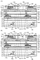
본 발명의 일 형태는 트랜지스터, 발광 다이오드, 제 1 도전층, 제 2 도전층, 제 1 절연층, 및 제 2 절연층을 가지는 표시 장치이다. 트랜지스터는 제 1 도전층과 전기적으로 접속되고, 제 1 도전층 및 제 1 절연층은 각각 트랜지스터 위에 위치한다. 제 2 도전층은 제 1 도전층 위에 위치한다. 제 2 절연층은 제 1 절연층 위에 위치한다. 발광 다이오드는 제 2 절연층 위의 제 1 전극과, 제 1 전극 위의 발광층과, 발광층 위의 제 2 전극을 가진다. 제 2 전극은 제 2 도전층과 전기적으로 접속된다. 제 1 도전층의 제 2 도전층 측의 면의 높이는 제 1 절연층의 제 2 절연층 측의 면의 높이와 실질적으로 일치한다. 제 1 절연층과 제 2 절연층은 직접 접합되어 있다. 제 2 도전층은 제 2 절연층의 개구 내부에 위치하며 제 1 도전층과 전기적으로 접속되어 있다.One embodiment of the present invention is a display device including a transistor, a light emitting diode, a first conductive layer, a second conductive layer, a first insulating layer, and a second insulating layer. The transistor is electrically connected to the first conductive layer, and the first conductive layer and the first insulating layer are each positioned over the transistor. The second conductive layer is located over the first conductive layer. The second insulating layer is located over the first insulating layer. The light emitting diode has a first electrode over the second insulating layer, a light emitting layer over the first electrode, and a second electrode over the light emitting layer. The second electrode is electrically connected to the second conductive layer. The height of the surface of the first conductive layer on the side of the second conductive layer substantially coincides with the height of the surface of the first insulating layer on the side of the second insulating layer. The first insulating layer and the second insulating layer are directly bonded. The second conductive layer is located inside the opening of the second insulating layer and is electrically connected to the first conductive layer.
본 발명의 일 형태의 표시 장치는 제 3 절연층 및 제 4 절연층을 더 가지는 것이 바람직하다. 제 3 절연층은 트랜지스터와 제 1 절연층 사이에 위치하는 것이 바람직하다. 제 4 절연층은 발광 다이오드와 제 2 절연층 사이에 위치하는 것이 바람직하다. 제 1 절연층 및 제 2 절연층은 각각 산화 실리콘막을 가지는 것이 바람직하다. 제 3 절연층 및 제 4 절연층은 각각 산화 알루미늄막, 산화 하프늄막, 및 질화 실리콘막 중 적어도 하나를 가지는 것이 바람직하다.It is preferable that the display device of one embodiment of the present invention further has a third insulating layer and a fourth insulating layer. The third insulating layer is preferably located between the transistor and the first insulating layer. The fourth insulating layer is preferably located between the light emitting diode and the second insulating layer. The first insulating layer and the second insulating layer preferably each have a silicon oxide film. Each of the third insulating layer and the fourth insulating layer preferably has at least one of an aluminum oxide film, a hafnium oxide film, and a silicon nitride film.
본 발명의 일 형태의 표시 장치는 제 5 절연층을 더 가지는 것이 바람직하다. 트랜지스터는 금속 산화물층 및 게이트 전극을 가지는 것이 바람직하다. 금속 산화물층은 채널 형성 영역을 가지는 것이 바람직하다. 게이트 전극의 상면의 높이는 제 5 절연층의 상면의 높이와 실질적으로 일치하는 것이 바람직하다.It is preferable that the display device of one embodiment of the present invention further has a fifth insulating layer. The transistor preferably has a metal oxide layer and a gate electrode. The metal oxide layer preferably has a channel formation region. The height of the upper surface of the gate electrode preferably substantially coincides with the height of the upper surface of the fifth insulating layer.
또는 트랜지스터는 금속 산화물층, 게이트 절연층, 게이트 전극, 제 3 도전층, 및 제 4 도전층을 가지는 것이 바람직하다. 금속 산화물층은 채널 형성 영역을 가지는 것이 바람직하다. 금속 산화물층은 제 3 도전층과 중첩되는 제 1 영역과, 제 4 도전층과 중첩되는 제 2 영역과, 제 1 영역과 제 2 영역 사이의 제 3 영역을 가지는 것이 바람직하다. 제 3 도전층과 제 4 도전층은 금속 산화물층 위에 서로 이격하여 위치하는 것이 바람직하다. 제 5 절연층은 제 3 도전층 위 및 제 4 도전층 위에 위치하는 것이 바람직하다. 제 5 절연층은 제 3 영역과 중첩되는 개구를 가지는 것이 바람직하다. 게이트 절연층은 개구의 내측에 위치하며 제 5 절연층의 측면 및 제 3 영역의 상면과 중첩되는 것이 바람직하다. 게이트 전극은 개구의 내측에 위치하며 게이트 절연층을 개재(介在)하여 제 5 절연층의 측면 및 제 3 영역의 상면과 중첩되는 것이 바람직하다.Alternatively, the transistor preferably has a metal oxide layer, a gate insulating layer, a gate electrode, a third conductive layer, and a fourth conductive layer. The metal oxide layer preferably has a channel formation region. The metal oxide layer preferably has a first region overlapping the third conductive layer, a second region overlapping the fourth conductive layer, and a third region between the first region and the second region. Preferably, the third conductive layer and the fourth conductive layer are spaced apart from each other on the metal oxide layer. The fifth insulating layer is preferably located on the third conductive layer and on the fourth conductive layer. The fifth insulating layer preferably has an opening overlapping the third region. Preferably, the gate insulating layer is located inside the opening and overlaps the side surface of the fifth insulating layer and the top surface of the third region. Preferably, the gate electrode is located inside the opening and overlaps the side surface of the fifth insulating layer and the top surface of the third region with the gate insulating layer interposed therebetween.
본 발명의 일 형태의 표시 장치는 구동 회로를 더 가지는 것이 바람직하다. 구동 회로는 회로용 트랜지스터를 가지는 것이 바람직하다. 회로용 트랜지스터는 반도체 기판에 채널 형성 영역을 가지는 것이 바람직하다. 트랜지스터, 발광 다이오드, 제 1 도전층, 제 2 도전층, 제 1 절연층, 및 제 2 절연층은 각각 반도체 기판 위에 위치하는 것이 바람직하다.It is preferable that the display device of one embodiment of the present invention further includes a driving circuit. The driving circuit preferably has a circuit transistor. The circuit transistor preferably has a channel formation region in a semiconductor substrate. Preferably, the transistor, the light emitting diode, the first conductive layer, the second conductive layer, the first insulating layer, and the second insulating layer are respectively located on the semiconductor substrate.
또는 트랜지스터는 반도체 기판에 채널 형성 영역을 가지는 것이 바람직하다. 반도체 기판은 실리콘 기판인 것이 바람직하다.Alternatively, the transistor preferably has a channel formation region in the semiconductor substrate. The semiconductor substrate is preferably a silicon substrate.
발광 다이오드는 마이크로 발광 다이오드인 것이 바람직하다. 또한, 발광 다이오드는 13족 원소 및 15족 원소를 포함하는 화합물(III-V족 화합물이라고도 함)을 가지는 것이 바람직하다. 또한, 발광 다이오드는 질화 갈륨을 가지는 것이 바람직하다.The light emitting diode is preferably a micro light emitting diode. In addition, the light emitting diode preferably has a compound (also referred to as a group III-V compound) containing a group 13 element and a group 15 element. Further, the light emitting diode preferably has gallium nitride.
본 발명의 일 형태의 표시 장치는 기능층을 더 가지는 것이 바람직하다. 기능층은 발광 다이오드 위에 위치하는 것이 바람직하다. 발광 다이오드가 발하는 광은 기능층을 통하여 상기 표시 장치의 외부로 추출되는 것이 바람직하다. 기능층은 착색층 및 색 변환층 중 한쪽 또는 양쪽을 가지는 것이 바람직하다.It is preferable that the display device of one embodiment of the present invention further has a functional layer. The functional layer is preferably located over the light emitting diode. Light emitted from the light emitting diode is preferably extracted to the outside of the display device through the functional layer. It is preferable that a functional layer has one or both of a coloring layer and a color conversion layer.
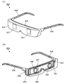
본 발명의 일 형태는 상기 구성의 표시 장치와, 광학 부재와, 프레임과, 하우징을 가지고, 하우징은 터치 센서를 가지는 전자 기기이다.One embodiment of the present invention is an electronic device comprising a display device having the above configuration, an optical member, a frame, and a housing, wherein the housing has a touch sensor.
본 발명의 일 형태는 상기 구성의 표시 장치를 가지는 표시 모듈이다. 상기 표시 모듈에는, 플렉시블 인쇄 회로 기판(Flexible Printed Circuit, 이하 FPC라고 기재함) 또는 TCP(Tape Carrier Package) 등의 커넥터가 장착되어도 좋다. 또한, 상기 표시 모듈에는 COG(Chip On Glass) 방식 또는 COF(Chip On Film) 방식 등에 의하여 집적 회로(IC)가 실장되어도 좋다.One embodiment of the present invention is a display module having the display device having the above configuration. A connector such as a flexible printed circuit board (hereinafter referred to as FPC) or a tape carrier package (TCP) may be attached to the display module. In addition, an integrated circuit (IC) may be mounted on the display module by a chip on glass (COG) method, a chip on film (COF) method, or the like.
본 발명의 일 형태는 상기 표시 모듈과, 안테나, 배터리, 하우징, 카메라, 스피커, 마이크로폰, 및 조작 버튼 중 적어도 하나를 가지는 전자 기기이다.One embodiment of the present invention is an electronic device including the display module, and at least one of an antenna, a battery, a housing, a camera, a speaker, a microphone, and an operation button.
본 발명의 일 형태는 제 1 기판 위에 복수의 트랜지스터를 형성하고, 복수의 트랜지스터 위에 각각 복수의 트랜지스터 중 적어도 하나와 전기적으로 접속되는 복수의 제 1 도전층을 형성하고, 복수의 트랜지스터 위에 제 1 절연층을 형성하고, 제 2 기판 위에 도전막, 제 1 반도체막, 발광체, 제 2 반도체막, 및 제 2 절연층을 이 순서대로 형성하고, 제 1 절연층과 제 2 절연층을 직접 접합시킴으로써 제 1 기판과 제 2 기판을 접합하고, 제 2 기판을 제 1 기판으로부터 박리하고, 도전막, 제 1 반도체막, 발광체, 및 제 2 반도체막을 가공함으로써 복수의 제 1 전극, 복수의 제 1 반도체층, 복수의 발광층, 및 복수의 제 2 반도체층을 매트릭스상으로 형성하고, 제 2 절연층에 각각 복수의 제 1 도전층 중 적어도 하나에 도달하는 복수의 개구를 형성하고, 각각 복수의 개구 중 적어도 하나의 내부에 위치하는 복수의 제 2 도전층을 형성하고, 각각 복수의 제 2 반도체층 중 적어도 하나 및 복수의 제 2 도전층 중 적어도 하나와 전기적으로 접속되는 복수의 제 2 전극을 형성함으로써 복수의 발광 다이오드를 형성하는 표시 장치의 제작 방법이다.In one embodiment of the present invention, a plurality of transistors are formed on a first substrate, a plurality of first conductive layers electrically connected to at least one of the plurality of transistors are respectively formed on the plurality of transistors, and a first insulation is formed on the plurality of transistors. layer is formed, a conductive film, a first semiconductor film, a light emitting body, a second semiconductor film, and a second insulating layer are formed in this order on the second substrate, and the first insulating layer and the second insulating layer are directly bonded The plurality of first electrodes and the plurality of first semiconductor layers are formed by bonding the first substrate and the second substrate, peeling the second substrate from the first substrate, and processing the conductive film, the first semiconductor film, the light emitting body, and the second semiconductor film. , a plurality of light emitting layers, and a plurality of second semiconductor layers are formed in a matrix, and a plurality of openings each reaching at least one of the plurality of first conductive layers are formed in the second insulating layer, respectively, at least of the plurality of openings By forming a plurality of second conductive layers positioned inside one, and forming a plurality of second electrodes electrically connected to at least one of the plurality of second semiconductor layers and at least one of the plurality of second conductive layers, respectively A method of manufacturing a display device for forming a light emitting diode of
복수의 트랜지스터를 형성하는 공정에서는 적어도 한 번의 평탄화 처리를 수행하는 것이 바람직하다. 복수의 발광 다이오드 중 적어도 하나는 마이크로 발광 다이오드인 것이 바람직하다. 복수의 트랜지스터 중 적어도 하나는 채널 형성 영역에 금속 산화물을 포함하는 것이 바람직하다. 복수의 트랜지스터 중 적어도 하나는 채널 형성 영역에 실리콘을 포함하는 것이 바람직하다.In the process of forming a plurality of transistors, it is preferable to perform at least one planarization process. At least one of the plurality of light emitting diodes is preferably a micro light emitting diode. At least one of the plurality of transistors preferably includes a metal oxide in the channel formation region. At least one of the plurality of transistors preferably includes silicon in a channel formation region.
본 발명의 일 형태의 표시 장치의 제작 방법에서는, 제 3 기판 위에 착색층, 색 변환층, 및 터치 센서 중 적어도 하나를 형성하고, 복수의 발광 다이오드 위에 제 3 기판을 접합하여도 좋다.In the method of manufacturing a display device of one embodiment of the present invention, at least one of a coloring layer, a color conversion layer, and a touch sensor may be formed on a third substrate, and the third substrate may be bonded over a plurality of light emitting diodes.
또는, 본 발명의 일 형태의 표시 장치의 제작 방법에서는, 복수의 발광 다이오드 중 적어도 하나 위에 착색층, 색 변환층, 및 터치 센서 중 적어도 하나를 형성하여도 좋다.Alternatively, in the method of manufacturing a display device of one embodiment of the present invention, at least one of a coloring layer, a color conversion layer, and a touch sensor may be formed on at least one of a plurality of light emitting diodes.
본 발명의 일 형태에 의하여 정세도가 높은 표시 장치를 제공할 수 있다. 본 발명의 일 형태에 의하여 해상도가 높은 표시 장치를 제공할 수 있다. 본 발명의 일 형태에 의하여 표시 품질이 높은 표시 장치를 제공할 수 있다. 본 발명의 일 형태에 의하여 소비 전력이 낮은 표시 장치를 제공할 수 있다. 본 발명의 일 형태에 의하여 신뢰성이 높은 표시 장치를 제공할 수 있다.According to one embodiment of the present invention, it is possible to provide a display device with high precision. According to one aspect of the present invention, it is possible to provide a display device having a high resolution. According to one embodiment of the present invention, a display device having high display quality can be provided. According to one embodiment of the present invention, a display device with low power consumption can be provided. According to one embodiment of the present invention, a highly reliable display device can be provided.
본 발명의 일 형태에 의하여, 표시 디바이스로서 마이크로 LED를 사용한 표시 장치의 제조 비용을 삭감할 수 있다. 본 발명의 일 형태에 의하여 마이크로 LED를 표시 디바이스에 사용한 표시 장치를 높은 수율로 제조할 수 있다.According to one embodiment of the present invention, the manufacturing cost of the display device using the microLED as the display device can be reduced. According to one embodiment of the present invention, a display device using a microLED for a display device can be manufactured with a high yield.
또한 이들 효과의 기재는 다른 효과의 존재를 방해하는 것이 아니다. 본 발명의 일 형태는 반드시 이들 효과 모두를 가질 필요는 없다. 명세서, 도면, 청구항의 기재로부터 이들 외의 효과를 추출할 수 있다.In addition, the description of these effects does not prevent the existence of other effects. One embodiment of the present invention does not necessarily have all of these effects. Other effects can be extracted from the description of the specification, drawings, and claims.
도 1은 표시 장치의 일례를 나타낸 단면도이다.
도 2는 표시 장치의 일례를 나타낸 단면도이다.
도 3의 (A), (B)는 표시 장치의 제작 방법의 일례를 나타낸 단면도이다.
도 4는 표시 장치의 제작 방법의 일례를 나타낸 단면도이다.
도 5는 표시 장치의 제작 방법의 일례를 나타낸 단면도이다.
도 6의 (A), (B)는 표시 장치의 제작 방법의 일례를 나타낸 단면도이다.
도 7의 (A), (B)는 표시 장치의 제작 방법의 일례를 나타낸 단면도이다.
도 8은 표시 장치의 일례를 나타낸 단면도이다.
도 9의 (A)는 트랜지스터의 일례를 나타낸 상면도이다. 도 9의 (B) 내지 (D)는 트랜지스터의 일례를 나타낸 단면도이다.
도 10은 화소의 일례를 나타낸 회로도이다.
도 11의 (A), (B)는 전자 기기의 일례를 나타낸 도면이다.
도 12의 (A), (B)는 전자 기기의 일례를 나타낸 도면이다.
도 13의 (A), (B)는 전자 기기의 일례를 나타낸 도면이다.
도 14의 (A) 내지 (D)는 전자 기기의 일례를 나타낸 도면이다.
도 15의 (A) 내지 (F)는 전자 기기의 일례를 나타낸 도면이다.1 is a cross-sectional view illustrating an example of a display device.
2 is a cross-sectional view illustrating an example of a display device.
3A and 3B are cross-sectional views illustrating an example of a method for manufacturing a display device.
4 is a cross-sectional view illustrating an example of a method of manufacturing a display device.
5 is a cross-sectional view illustrating an example of a method of manufacturing a display device.
6A and 6B are cross-sectional views illustrating an example of a method for manufacturing a display device.
7A and 7B are cross-sectional views illustrating an example of a method for manufacturing a display device.
8 is a cross-sectional view illustrating an example of a display device.
9A is a top view showing an example of a transistor. 9B to 9D are cross-sectional views showing an example of a transistor.
10 is a circuit diagram illustrating an example of a pixel.
11A and 11B are diagrams showing an example of an electronic device.
12A and 12B are diagrams showing an example of an electronic device.
13A and 13B are diagrams showing an example of an electronic device.
14A to 14D are views showing an example of an electronic device.
15A to 15F are diagrams showing an example of an electronic device.
실시형태에 대하여 도면을 사용하여 자세히 설명한다. 다만 본 발명은 이하의 설명에 한정되지 않고, 본 발명의 취지 및 그 범위에서 벗어남이 없이 그 형태 및 자세한 사항을 다양하게 변경할 수 있다는 것은 통상의 기술자라면 용이하게 이해할 수 있다. 따라서 본 발명은 이하의 실시형태의 기재 내용에 한정하여 해석되는 것이 아니다.EMBODIMENT OF THE INVENTION It demonstrates in detail using drawing about embodiment. However, the present invention is not limited to the following description, and it can be easily understood by those skilled in the art that various changes can be made in the form and details without departing from the spirit and scope of the present invention. Therefore, this invention is limited to the description of the following embodiment, and is not interpreted.
또한 이하에서 설명하는 발명의 구성에서, 동일한 부분 또는 같은 기능을 가지는 부분에는 동일한 부호를 상이한 도면 사이에서 공통적으로 사용하고, 이에 대한 반복적인 설명은 생략한다. 또한 같은 기능을 가지는 부분을 가리키는 경우에는 해치 패턴을 동일하게 하고, 특별히 부호를 붙이지 않는 경우가 있다.In addition, in the configuration of the invention described below, the same reference numerals are commonly used between different drawings for the same parts or parts having the same function, and a repetitive description thereof will be omitted. In addition, when referring to parts having the same function, the hatch pattern is made the same, and there are cases in which no particular sign is attached.
또한 도면에 나타낸 각 구성의 위치, 크기, 범위 등은 이해를 쉽게 하기 위하여 실제의 위치, 크기, 범위 등을 나타내지 않는 경우가 있다. 그러므로 개시(開示)된 발명은 반드시 도면에 개시된 위치, 크기, 범위 등에 한정되는 것은 아니다.In addition, the location, size, range, etc. of each component shown in the drawings may not represent the actual location, size, range, etc. for easy understanding. Therefore, the disclosed invention is not necessarily limited to the position, size, scope, etc. disclosed in the drawings.
또한 "막"이라는 용어와 "층"이라는 용어는 경우 또는 상황에 따라 서로 바꿀 수 있다. 예를 들어 "도전층"이라는 용어를 "도전막"이라는 용어로 변경할 수 있다. 또는 예를 들어 "절연막"이라는 용어를 "절연층"이라는 용어로 변경할 수 있다.Also, the terms "membrane" and "layer" may be used interchangeably depending on the case or situation. For example, the term "conductive layer" may be changed to the term "conductive film". Or, for example, the term “insulating film” may be changed to the term “insulating layer”.
(실시형태 1)(Embodiment 1)
본 실시형태에서는 본 발명의 일 형태의 표시 장치에 대하여 도 1 내지 도 8을 사용하여 설명한다.In the present embodiment, a display device of one embodiment of the present invention will be described with reference to FIGS. 1 to 8 .
본 실시형태의 표시 장치는 표시 디바이스인 발광 다이오드와, 표시 디바이스를 구동하는 트랜지스터를 각각 복수로 가진다. 복수의 발광 다이오드는 매트릭스상으로 제공되어 있다. 복수의 트랜지스터는 각각 복수의 발광 다이오드 중 적어도 하나에 전기적으로 접속된다.The display device of the present embodiment includes a light emitting diode as a display device and a plurality of transistors for driving the display device, respectively. A plurality of light emitting diodes are provided in a matrix form. Each of the plurality of transistors is electrically connected to at least one of the plurality of light emitting diodes.
본 실시형태의 표시 장치의 제작 방법에서는, 서로 다른 기판 위에 형성된 발광 다이오드를 구성하는 적층막과 복수의 트랜지스터를 접합한 후에, 상기 적층막을 가공하여 소자 분리(아이솔레이션(isolation)이라고도 함)함으로써 복수의 발광 다이오드를 형성한다.In the method of manufacturing the display device of the present embodiment, after bonding a plurality of transistors to a laminated film constituting a light emitting diode formed on different substrates, the laminated film is processed to isolate the elements (also referred to as isolation) to form a plurality of to form a light emitting diode.
본 실시형태의 표시 장치의 제작 방법에서는, 발광 다이오드를 구성하는 적층막을 가공하기 전에 상기 적층막이 형성된 기판과 트랜지스터가 형성된 기판을 접합하기 때문에, 접합하는 데 높은 위치 맞춤 정밀도가 요구되지 않는다. 따라서, 화소수가 많은 표시 장치 또는 고정세(高精細)의 표시 장치를 제작하는 경우에도 접합의 난도를 낮출 수 있어, 표시 장치의 제작 수율을 높일 수 있다.In the manufacturing method of the display device of this embodiment, since the substrate on which the laminated film is formed and the substrate on which the transistor is formed are bonded before the laminated film constituting the light emitting diode is processed, high alignment accuracy is not required for bonding. Accordingly, even when a display device having a large number of pixels or a high-definition display device is manufactured, the difficulty of bonding can be lowered and the manufacturing yield of the display device can be increased.
본 발명의 일 형태의 표시 장치의 제작 방법으로서는, 우선 제 1 기판 위에 복수의 트랜지스터를 매트릭스상으로 형성하고, 복수의 트랜지스터 위에 제 1 절연층과 복수의 제 1 도전층을 형성한다. 여기서, 제 1 절연층의 상면의 높이와 제 1 도전층의 상면의 높이가 일치하도록 제 1 절연층 및 제 1 도전층을 형성한다. 복수의 제 1 도전층은 각각 복수의 트랜지스터 중 적어도 하나와 전기적으로 접속된다. 또한, 제 2 기판 위에 도전막, 제 1 반도체막, 발광체, 제 2 반도체막, 및 제 2 절연층을 이 순서대로 형성한다.In a method of manufacturing a display device of one embodiment of the present invention, first, a plurality of transistors are formed in a matrix form on a first substrate, and a first insulating layer and a plurality of first conductive layers are formed on the plurality of transistors. Here, the first insulating layer and the first conductive layer are formed so that the height of the upper surface of the first insulating layer coincides with the height of the upper surface of the first conductive layer. Each of the plurality of first conductive layers is electrically connected to at least one of the plurality of transistors. Further, on the second substrate, a conductive film, a first semiconductor film, a light emitting body, a second semiconductor film, and a second insulating layer are formed in this order.
다음으로, 제 1 절연층과 제 2 절연층을 직접 접합시킴으로써 제 1 기판과 제 2 기판을 접합한다. 제 1 절연층과 제 2 절연층은 동일한 재료로 형성되는 것이 바람직하고, 특히, 제 1 절연층과 제 2 절연층으로서 산화 실리콘막을 사용하는 것이 바람직하다. 수산기(OH기)를 통한 친수성 접합이 일어남으로써, 제 1 절연층과 제 2 절연층의 접합 강도를 높일 수 있다. 도전막, 제 1 반도체막, 발광체, 및 제 2 반도체막의 가공 전(발광 다이오드의 소자 분리 전)에 제 1 기판과 제 2 기판을 접합시킨 경우 높은 위치 맞춤 정밀도가 요구되지 않기 때문에 접합의 난도를 낮출 수 있어, 표시 장치의 제작 수율을 높일 수 있다.Next, the first substrate and the second substrate are bonded by directly bonding the first insulating layer and the second insulating layer. The first insulating layer and the second insulating layer are preferably formed of the same material, and in particular, it is preferable to use a silicon oxide film as the first insulating layer and the second insulating layer. When hydrophilic bonding occurs through a hydroxyl group (OH group), the bonding strength between the first insulating layer and the second insulating layer can be increased. When the first substrate and the second substrate are joined before the processing of the conductive film, the first semiconductor film, the light emitting body, and the second semiconductor film (before separation of the light emitting diode element), high positioning accuracy is not required, so the difficulty of bonding is reduced. It can be lowered, so that the manufacturing yield of the display device can be increased.
다음으로, 제 2 기판을 제 1 기판으로부터 박리한다. 그리고, 도전막, 제 1 반도체막, 발광체, 및 제 2 반도체막을 각각 복수의 섬 형상의 패턴으로 가공함으로써 복수의 제 1 전극, 복수의 제 1 반도체층, 복수의 발광층, 및 복수의 제 2 반도체층을 매트릭스상으로 형성한다. 제 1 전극, 제 1 반도체층, 발광층, 및 제 2 반도체층은 각각 발광 다이오드를 구성하는 층이다.Next, the second substrate is peeled from the first substrate. Then, a plurality of first electrodes, a plurality of first semiconductor layers, a plurality of light emitting layers, and a plurality of second semiconductors are processed by processing the conductive film, the first semiconductor film, the light emitting body, and the second semiconductor film into a plurality of island-shaped patterns, respectively. The layer is formed into a matrix phase. The first electrode, the first semiconductor layer, the light emitting layer, and the second semiconductor layer are layers constituting the light emitting diode, respectively.
다음으로, 제 2 절연층에 복수의 개구를 형성한다. 복수의 개구는 각각 복수의 제 1 도전층 중 적어도 하나에 도달한다. 다음으로, 복수의 제 2 도전층을 형성한다. 복수의 제 2 도전층은 각각 복수의 개구 중 적어도 하나의 내부에 위치한다. 이에 의하여, 제 1 도전층과 제 2 도전층이 서로 전기적으로 접속된다.Next, a plurality of openings are formed in the second insulating layer. The plurality of openings each reach at least one of the plurality of first conductive layers. Next, a plurality of second conductive layers are formed. Each of the plurality of second conductive layers is positioned inside at least one of the plurality of openings. Thereby, the first conductive layer and the second conductive layer are electrically connected to each other.
그리고, 복수의 제 2 전극을 형성한다. 제 2 전극은 제 2 반도체층 및 제 2 도전층과 전기적으로 접속된다. 이에 의하여, 제 1 전극, 제 1 반도체층, 발광층, 제 2 반도체층, 및 제 2 전극을 가지는 발광 다이오드를 복수 개 형성할 수 있다. 제 2 전극은 제 2 반도체층의 상면 및 제 2 도전층의 상면과 접하도록 형성되는 것이 바람직하다. 또한, 제 2 전극은 제 1 도전층 및 제 2 도전층을 통하여 트랜지스터와 전기적으로 접속된다. 이에 의하여, 복수의 트랜지스터의 각각이 복수의 발광 다이오드 중 적어도 하나와 전기적으로 접속된다.Then, a plurality of second electrodes are formed. The second electrode is electrically connected to the second semiconductor layer and the second conductive layer. Thereby, a plurality of light emitting diodes having a first electrode, a first semiconductor layer, a light emitting layer, a second semiconductor layer, and a second electrode can be formed. The second electrode is preferably formed so as to be in contact with the upper surface of the second semiconductor layer and the upper surface of the second conductive layer. Further, the second electrode is electrically connected to the transistor via the first conductive layer and the second conductive layer. Thereby, each of the plurality of transistors is electrically connected to at least one of the plurality of light emitting diodes.
제작된 표시 장치에서, 제 1 도전층의 제 2 도전층 측의 면의 높이는, 제 1 절연층의 제 2 절연층 측의 면의 높이와 실질적으로 일치한다. 또한, 본 명세서 등에 있어서, "A와 B가 실질적으로 일치한다"란, A와 B가 일치하는 경우를 포함하며 A와 B가 일치하도록 제작되었을 때의 제조상의 오차에 의하여 A와 B 사이에 차이가 생긴 경우를 포함한다.In the manufactured display device, the height of the surface of the first conductive layer on the side of the second conductive layer substantially coincides with the height of the surface of the first insulating layer on the side of the second insulation layer. In addition, in this specification and the like, "A and B substantially match" includes cases where A and B match, and the difference between A and B due to manufacturing errors when A and B are manufactured to match including cases where
본 발명의 일 형태의 표시 장치는 제 3 절연층 및 제 4 절연층을 더 가지는 것이 바람직하다. 제 3 절연층은 트랜지스터와 제 1 절연층 사이에 위치하는 것이 바람직하다. 제 4 절연층은 발광 다이오드와 제 2 절연층 사이에 위치하는 것이 바람직하다. 제 3 절연층 및 제 4 절연층으로서는 제 1 절연층 및 제 2 절연층보다 수소 및 산소 중 한쪽 또는 양쪽이 확산되기 어려운 막을 사용하는 것이 바람직하다. 제 3 절연층 및 제 4 절연층은 각각 산화 알루미늄막, 산화 하프늄막, 및 질화 실리콘막 중 적어도 하나를 가지는 것이 바람직하다. 산화 실리콘막보다 수소 및 산소 중 한쪽 또는 양쪽이 확산되기 어려운 막을 사용함으로써, 제 1 기판 측의 적층 구조 및 제 2 기판 측의 적층 구조 중 한쪽으로부터 다른 쪽으로 불순물이 확산되는 것 등을 억제할 수 있다.It is preferable that the display device of one embodiment of the present invention further has a third insulating layer and a fourth insulating layer. The third insulating layer is preferably located between the transistor and the first insulating layer. The fourth insulating layer is preferably located between the light emitting diode and the second insulating layer. As the third insulating layer and the fourth insulating layer, it is preferable to use a film in which one or both of hydrogen and oxygen are more difficult to diffuse than the first insulating layer and the second insulating layer. Each of the third insulating layer and the fourth insulating layer preferably has at least one of an aluminum oxide film, a hafnium oxide film, and a silicon nitride film. By using a film in which one or both of hydrogen and oxygen are more difficult to diffuse than the silicon oxide film, diffusion of impurities from one of the laminated structure on the first substrate side and the laminated structure on the second substrate side to the other can be suppressed. .
본 실시형태의 표시 장치는 발광 다이오드를 사용하여 영상을 표시하는 기능을 가진다. 발광 다이오드는 자발광 디바이스이기 때문에, 표시 디바이스로서 발광 다이오드를 사용하는 경우, 표시 장치에는 백라이트가 불필요하고, 또한 편광판을 제공하지 않아도 된다. 따라서, 표시 장치의 소비 전력을 저감할 수 있고, 또한 표시 장치의 박형·경량화가 가능하다. 또한, 표시 디바이스로서 발광 다이오드를 사용한 표시 장치는 휘도를 높일 수 있고(예를 들어, 5000cd/m2 이상, 바람직하게는 10000cd/m2 이상), 또한 콘트라스트가 높고 시야각이 넓기 때문에, 높은 표시 품질을 얻을 수 있다. 또한 발광 재료로서 무기 재료를 사용함으로써, 표시 장치의 수명을 길게 하고, 신뢰성을 높일 수 있다.The display device of this embodiment has a function of displaying an image using a light emitting diode. Since a light emitting diode is a self-light emitting device, when using a light emitting diode as a display device, a backlight is unnecessary for a display apparatus, and it is not necessary to provide a polarizing plate. Accordingly, power consumption of the display device can be reduced, and the display device can be made thinner and lighter. In addition, a display device using a light emitting diode as a display device can increase luminance (for example, 5000 cd/m 2 or more, preferably 10000 cd/m 2 or more), and has high contrast and wide viewing angle, so high display quality can get Moreover, by using an inorganic material as a light emitting material, the lifetime of a display apparatus can be lengthened and reliability can be improved.
본 실시형태에서는 특히 발광 다이오드로서 마이크로 LED를 사용하는 경우의 예에 대하여 설명한다. 또한 본 실시형태에서는 더블 헤테로 접합을 가지는 마이크로 LED에 대하여 설명한다. 다만 발광 다이오드에 특별한 한정은 없고, 예를 들어 양자 우물 접합을 가지는 마이크로 LED, 나노 칼럼을 사용한 LED 등을 사용하여도 좋다.In this embodiment, an example in which a microLED is used as the light emitting diode will be particularly described. In addition, in this embodiment, the micro LED which has a double heterojunction is demonstrated. However, there is no particular limitation on the light emitting diode, and for example, a micro LED having a quantum well junction, an LED using a nano column, or the like may be used.
발광 다이오드의 광이 사출되는 영역의 면적은 1mm2 이하가 바람직하고, 10000μm2 이하가 더 바람직하고, 3000μm2 이하가 더욱 바람직하고, 700μm2 이하가 더욱더 바람직하다. 또한 본 명세서 등에서, 광이 사출되는 영역의 면적이 10000μm2 이하인 발광 다이오드를 마이크로 LED라고 기재하는 경우가 있다.The area of the region from which light of the light emitting diode is emitted is preferably 1 mm 2 or less, more preferably 10000 μm 2 or less, still more preferably 3000 μm 2 or less, and still more preferably 700 μm 2 or less. In addition, in this specification and the like, a light emitting diode having an area of 10000 µm 2 or less in a region from which light is emitted may be referred to as a micro LED.
표시 장치가 가지는 트랜지스터는 채널 형성 영역에 금속 산화물을 포함하는 것이 바람직하다. 금속 산화물이 사용된 트랜지스터는 소비 전력이 저감될 수 있다. 그러므로 마이크로 LED와 조합함으로써, 소비 전력이 매우 저감된 표시 장치를 실현할 수 있다.The transistor of the display device preferably includes a metal oxide in the channel formation region. A transistor in which a metal oxide is used can reduce power consumption. Therefore, by combining with the micro LED, a display device with extremely reduced power consumption can be realized.
특히 본 실시형태의 표시 장치는, 게이트 전극의 상면의 높이가 절연층의 상면의 높이와 실질적으로 일치하는 트랜지스터를 가지는 것이 바람직하다. 예를 들어 CMP(Chemical Mechanical Polishing)법 등을 사용하여 평탄화 처리를 실시함으로써, 게이트 전극의 상면과 절연층의 상면을 평탄화하여, 게이트 전극의 상면의 높이와 절연층의 상면의 높이를 일치시킬 수 있다.In particular, it is preferable that the display device of this embodiment has a transistor in which the height of the upper surface of the gate electrode substantially coincides with the height of the upper surface of the insulating layer. For example, by performing a planarization process using a chemical mechanical polishing (CMP) method or the like, the upper surface of the gate electrode and the upper surface of the insulating layer are planarized so that the height of the upper surface of the gate electrode and the upper surface of the insulating layer are equal. have.
이와 같은 구성의 트랜지스터는 크기를 축소하기 쉽다. 트랜지스터의 크기를 축소함으로써, 화소의 크기를 축소할 수 있기 때문에, 표시 장치의 정세도를 높일 수 있다.A transistor having such a configuration is easy to reduce in size. By reducing the size of the transistor, the size of the pixel can be reduced, so that the definition of the display device can be improved.
또는, 표시 장치가 가지는 트랜지스터는 채널 형성 영역에 실리콘을 포함하는 것이 바람직하다. 이에 의하여, 회로의 고속 동작이 가능하다.Alternatively, the transistor of the display device preferably includes silicon in the channel formation region. Thereby, high-speed operation of the circuit is possible.
또한, 표시 장치는 채널 형성 영역에 실리콘을 포함하는 트랜지스터와, 채널 형성 영역에 금속 산화물을 가지는 트랜지스터의 양쪽을 가져도 좋다. 예를 들어, 화소 회로 및 게이트 드라이버에 채널 형성 영역에 금속 산화물을 가지는 트랜지스터를 사용하고, 소스 드라이버에 채널 형성 영역에 실리콘을 포함하는 트랜지스터를 사용하여도 좋다. 또는, 예를 들어, 화소 회로에 채널 형성 영역에 금속 산화물을 가지는 트랜지스터를 사용하고, 소스 드라이버 및 게이트 드라이버에 채널 형성 영역에 실리콘을 포함하는 트랜지스터를 사용하여도 좋다. 또는, 화소 회로, 게이트 드라이버, 및 소스 드라이버 모두에 채널 형성 영역에 실리콘을 포함하는 트랜지스터를 사용하여도 좋다. 또는, 화소 회로, 게이트 드라이버, 및 소스 드라이버 모두에 채널 형성 영역에 금속 산화물을 가지는 트랜지스터를 사용하여도 좋다.Further, the display device may include both a transistor including silicon in the channel formation region and a transistor including a metal oxide in the channel formation region. For example, a transistor having a metal oxide may be used in the channel formation region for the pixel circuit and the gate driver, and a transistor containing silicon in the channel formation region may be used for the source driver. Alternatively, for example, in the pixel circuit, a transistor having a metal oxide may be used in the channel formation region, and a transistor including silicon in the channel formation region may be used for the source driver and the gate driver. Alternatively, a transistor including silicon in the channel formation region may be used for all of the pixel circuit, the gate driver, and the source driver. Alternatively, a transistor having a metal oxide in the channel formation region may be used for all of the pixel circuit, the gate driver, and the source driver.
본 실시형태의 표시 장치는 정세도를 높일 수 있기 때문에, 비교적 작은 표시부를 가지는 전자 기기에 적합하게 사용할 수 있다. 이와 같은 전자 기기로서는, 예를 들어 손목시계형 및 팔찌형 정보 단말기(웨어러블 기기)가 있다. 상기 외에, 이와 같은 전자 기기로서 헤드 마운트 디스플레이 등의 VR(Virtual Reality)용 기기, 안경형 AR(Augmented Reality)용 기기, 및 MR(Mixed Reality)용 기기 등의 머리에 장착할 수 있는 웨어러블 기기 등이 있다.Since the display device of the present embodiment can improve the precision, it can be suitably used for electronic devices having a relatively small display unit. As such an electronic device, there exist a wrist watch type and a wristband type information terminal (wearable device), for example. In addition to the above, as such electronic devices, there are wearable devices that can be mounted on the head, such as devices for VR (Virtual Reality) such as a head mounted display, glasses-type AR (Augmented Reality) devices, and MR (Mixed Reality) devices. have.
[표시 장치의 구성예 1][Configuration example 1 of display device]
도 1은 표시 장치(100A)의 단면도이다. 도 2는 표시 장치(100B)의 단면도이다. 도 3 내지 도 7은 표시 장치(100A) 및 표시 장치(100B)의 제작 방법을 나타낸 단면도이다. 이하에서는, 표시 장치(100A 및 100B)의 구성 및 제작 방법에 대하여 설명한다.1 is a cross-sectional view of a display device 100A. 2 is a cross-sectional view of the display device 100B. 3 to 7 are cross-sectional views illustrating a
표시 장치(100A) 및 표시 장치(100B)는 채널 형성 영역에 실리콘을 포함하는 트랜지스터(130a, 130b)와, 채널 형성 영역에 금속 산화물을 가지는 트랜지스터(120a, 120b)와, 발광 다이오드(110a, 110b)를 가진다.The
발광 다이오드(110a)는 전극(112a), 반도체층(113a), 발광층(114a), 반도체층(115a), 및 전극(117a)을 가진다. 발광 다이오드(110b)는 전극(112b), 반도체층(113b), 발광층(114b), 반도체층(115b), 및 전극(117c)을 가진다. 발광 다이오드가 가지는 각 층은 단층 구조이어도 좋고, 적층 구조이어도 좋다.The
표시 장치(100A) 및 표시 장치(100B)에서, 각 색의 부화소는 동일한 색의 광을 나타내는 발광 다이오드를 가진다. 본 실시형태에서는 각 색의 부화소가 청색의 광을 나타내는 발광 다이오드를 가지는 예를 들어 설명한다.In the
표시 장치(100A) 및 표시 장치(100B)에서, 적색의 부화소가 가지는 발광 다이오드(110a)와 중첩되는 영역에 착색층(CFR) 및 색 변환층(CCMR)이 제공되어 있다. 색 변환층(CCMR)은 청색의 광을 적색의 광으로 변환하는 기능을 가진다.In the
발광 다이오드(110a)가 발한 광은 색 변환층(CCMR)에 의하여 청색으로부터 적색으로 변환되고, 착색층(CFR)에 의하여 적색의 광의 순도가 높아지고, 표시 장치(100A) 또는 표시 장치(100B)의 외부로 사출된다.The light emitted by the
도시하지 않았지만, 마찬가지로 표시 장치(100A) 및 표시 장치(100B)에서, 녹색의 부화소가 가지는 발광 다이오드와 중첩되는 영역에 녹색의 착색층과, 청색의 광을 녹색으로 변환하는 색 변환층이 제공되어 있다. 따라서 녹색의 부화소가 가지는 발광 다이오드가 발하는 광은 색 변환층에 의하여 청색으로부터 녹색으로 변환되고, 착색층에 의하여 녹색의 광의 순도가 높아지고, 표시 장치(100A) 또는 표시 장치(100B)의 외부로 사출된다.Although not shown, similarly, in the
한편, 표시 장치(100A) 또는 표시 장치(100B)에서, 청색의 부화소가 가지는 발광 다이오드(110b)와 중첩되는 영역에는 색 변환층이 제공되지 않는다. 발광 다이오드(110b)가 발한 청색의 광은 색이 변환되지 않고 표시 장치(100A) 또는 표시 장치(100B)의 외부로 사출된다.Meanwhile, in the
또한, 표시 장치(100A) 또는 표시 장치(100B)에서, 청색의 화소가 가지는 발광 다이오드(110b)와 중첩되는 영역에 청색의 착색층이 제공되어도 좋다. 청색의 착색층을 제공하면, 청색의 광의 순도를 높일 수 있다. 또한, 청색의 착색층을 제공하지 않는 경우, 제작 공정을 간략화할 수 있다.Further, in the
각 색의 부화소에 구성이 같은 발광 다이오드를 가지는 표시 장치의 제작에서는, 기판 위에 1종류의 발광 다이오드만을 제작하면 되기 때문에, 복수 종류의 발광 다이오드를 제작하는 경우에 비하여 제조 장치 및 공정을 간이화할 수 있다.In manufacturing a display device having light emitting diodes having the same structure in subpixels of each color, since only one type of light emitting diode needs to be manufactured on a substrate, the manufacturing apparatus and process can be simplified compared to the case of manufacturing multiple types of light emitting diodes. can
본 실시형태의 표시 장치에서는, 도 1 및 도 2에 나타낸 화살표의 방향으로 적색의 광(R)과 청색의 광(B)이 추출된다. 표시 장치(100A)에서, 발광 다이오드(110a)가 발하는 광은 발광 다이오드(110a) 위에 형성된 색 변환층(CCMR) 및 착색층(CFR)을 통하여 추출된다. 한편, 표시 장치(100B)에서는, 발광 다이오드(110a) 위에 기판(191)이 접합되어 있고, 발광 다이오드(110a)가 발하는 광은 상기 기판(191)에 형성된 색 변환층(CCMR) 및 착색층(CFR)을 통하여 추출된다.In the display device of the present embodiment, red light R and blue light B are extracted in the direction of the arrows shown in FIGS. 1 and 2 . In the
본 실시형태의 표시 장치의 제작 방법으로서는, 우선 도 3의 (A)에 나타낸 LED 기판(150A)과, 도 3의 (B)에 나타낸 회로 기판(150B)을 각각 제작한다.As a manufacturing method of the display device of this embodiment, first, the
도 3의 (A)는 LED 기판(150A)의 단면도이다.3A is a cross-sectional view of the
LED 기판(150A)은 기판(101), 반도체막(115), 발광체(114), 반도체막(113), 도전막(112), 절연층(103), 및 절연층(104)을 가진다. 반도체막(115), 발광체(114), 반도체막(113), 도전막(112), 절연층(103), 및 절연층(104)은 각각 단층 구조이어도 좋고, 적층 구조이어도 좋다. LED 기판(150A)은 층을 더 가져도 좋다. 예를 들어, 기판(101)과 반도체막(115) 사이에 하지층 등이 제공되어도 좋다.The
도전막(112), 반도체막(113), 발광체(114), 및 반도체막(115)은 나중의 공정에서 가공되어 발광 다이오드를 구성하는 막이다. 발광체(114)는 반도체막(113)과 반도체막(115)에 끼워져 있다. 발광체(114)에서는, 전자와 정공이 결합하여 광을 발한다. 반도체막(113) 및 반도체막(115) 중 한쪽은 n형의 반도체층이고, 다른 쪽은 p형의 반도체층이다.The
반도체막(113), 발광체(114), 및 반도체막(115)을 포함하는 적층 구조는 적색, 황색, 녹색, 청색, 자외광 등의 광을 나타내도록 형성된다. 이들의 적층 구조에는, 예를 들어 13족 원소 및 15족 원소를 포함하는 화합물(III-V족 화합물이라고도 함)을 사용할 수 있다. 13족 원소로서는 알루미늄, 갈륨, 인듐 등을 들 수 있다. 15족 원소로서는 질소, 인, 비소, 안티모니 등을 들 수 있다. 예를 들어, 갈륨·인 화합물, 갈륨·비소 화합물, 갈륨·알루미늄·비소 화합물, 알루미늄·갈륨·인듐·인 화합물, 질화 갈륨(GaN), 인듐·질화 갈륨 화합물, 셀레늄·아연 화합물 등을 사용하여 발광 다이오드를 제작할 수 있다.The stacked structure including the
기판(101)으로서는, 화합물 반도체 기판을 사용하여도 좋고, 예를 들어 13족 원소 및 15족 원소를 포함하는 화합물 반도체 기판을 사용하여도 좋다. 또한 기판(101)으로서는, 예를 들어 사파이어(Al2O3) 기판, 탄소화 실리콘(SiC) 기판, 실리콘(Si) 기판, 질화 갈륨(GaN) 기판 등의 단결정 기판을 사용할 수 있다.As the
도전막(112)은 나중의 공정에서 가공되어 발광 다이오드의 전극이 되는 막이다. 도전막(112)에 사용할 수 있는 재료로서는, 예를 들어 알루미늄, 타이타늄, 크로뮴, 니켈, 구리, 이트륨, 지르코늄, 주석, 아연, 은, 백금, 금, 몰리브데넘, 탄탈럼, 또는 텅스텐 등의 금속, 또는 이들을 주성분으로 하는 합금(은과 팔라듐과 구리의 합금(Ag-Pd-Cu(APC) 등)이 있다. 또한, 산화 주석 또는 산화 아연 등의 산화물을 사용하여도 좋다.The
절연층(103) 및 절연층(104)은 산화 실리콘, 산화질화 실리콘, 질화산화 실리콘, 질화 실리콘, 산화 알루미늄, 산화 하프늄, 질화 타이타늄 등의 각종 무기 절연 재료를 사용하여 형성할 수 있다.The insulating
또한 본 명세서 등에서 산화질화 실리콘이란 그 조성으로서 질소보다 산소의 함유량이 많은 것을 말한다. 또한 질화산화 실리콘이란 그 조성으로서 산소보다 질소의 함유량이 많은 것을 말한다.In addition, in this specification, etc., silicon oxynitride means that content of oxygen is more than nitrogen as its composition. In addition, silicon nitride oxide means that the content of nitrogen is greater than oxygen as its composition.
특히, 절연층(103)에는 예를 들어 산화 알루미늄막, 산화 하프늄막, 질화 실리콘막 등, 산화 실리콘막보다 수소 및 산소 중 한쪽 또는 양쪽이 확산되기 어려운 막을 사용하는 것이 바람직하다. 절연층(103)은 LED 기판(150A)으로부터 회로 기판(150B)으로 불순물이 확산되는 것을 방지하는 배리어층으로서 기능하는 것이 바람직하다.In particular, it is preferable to use a film in which one or both of hydrogen and oxygen are more difficult to diffuse than a silicon oxide film, such as an aluminum oxide film, a hafnium oxide film, or a silicon nitride film, for example, for the insulating
또한, 절연층(104)에는 산화물 절연막을 사용하는 것이 바람직하다. 절연층(104)은 회로 기판(150B)이 가지는 절연층과 직접 접합하는 층이다. 산화물 절연막들을 직접 접합시킴으로써 접합 강도를 높일 수 있다.In addition, it is preferable to use an oxide insulating film for the insulating
또한 본 실시형태의 표시 장치는 적외광을 나타내는 발광 다이오드를 가져도 좋다. 적외광을 나타내는 발광 다이오드는, 예를 들어 적외광 센서의 광원으로서 사용될 수 있다.In addition, the display device of this embodiment may have a light emitting diode which shows infrared light. A light emitting diode that exhibits infrared light can be used, for example, as a light source of an infrared light sensor.
도 3의 (B)는 회로 기판(150B)의 단면도이다.3B is a cross-sectional view of the
회로 기판(150B)은 기판(131)에 채널 형성 영역을 가지는 트랜지스터(트랜지스터(130a, 130b))와, 금속 산화물에 채널 형성 영역을 가지는 트랜지스터(트랜지스터(120a, 120b))의 적층을 가진다. 또한, 회로 기판(150B)이 가지는 각층은 단층 구조이어도 좋고, 적층 구조이어도 좋다.The
기판(131)으로서는 단결정 실리콘 기판이 적합하다. 트랜지스터(130a, 130b)는 도전층(135), 절연층(134), 절연층(136), 한 쌍의 저저항 영역(133)을 가진다. 도전층(135)은 게이트로서 기능한다. 절연층(134)은 도전층(135)과 기판(131) 사이에 위치하고, 게이트 절연층으로서 기능한다. 절연층(136)은 도전층(135)의 측면을 덮어 제공되고, 측벽으로서 기능한다. 한 쌍의 저저항 영역(133)은 기판(131)에서 불순물이 도핑된 영역이고, 한쪽이 트랜지스터의 소스로서 기능하고, 다른 쪽이 트랜지스터의 드레인으로서 기능한다.As the
또한 기판(131)에 매립되도록, 인접한 2개의 트랜지스터 사이에 소자 분리층(132)이 제공되어 있다.Also, a
트랜지스터(130a, 130b)를 덮어 절연층(139)이 제공되고, 절연층(139) 위에 도전층(138)이 제공되어 있다. 절연층(139)의 개구에 매립된 도전층(137)을 통하여, 도전층(138)은 한 쌍의 저저항 영역(133) 중 한쪽에 전기적으로 접속된다. 또한 도전층(138)을 덮어 절연층(141)이 제공되고, 절연층(141) 위에 도전층(142)이 제공되어 있다. 도전층(138) 및 도전층(142)은 각각 배선으로서 기능한다. 또한 도전층(142)을 덮어 절연층(143) 및 절연층(152)이 제공되고, 절연층(152) 위에 트랜지스터(120a, 120b)가 제공되어 있다.An insulating
트랜지스터(130a, 130b)와 트랜지스터(120a, 120b) 사이에 제공되는 절연층(도 3의 (B)에서는 절연층(139), 절연층(141), 절연층(143), 및 절연층(152)) 중 적어도 하나의 층으로서 배리어층으로서 기능하는 층을 사용하는 것이 바람직하다. 배리어층으로서는, 예를 들어 산화 알루미늄막, 산화 하프늄막, 질화 실리콘막 등, 산화 실리콘막보다 수소 및 산소 중 한쪽 또는 양쪽이 확산되기 어려운 막을 사용하는 것이 바람직하다. 본 실시형태에서는 절연층(152)이 배리어층으로서 기능하는 예를 나타낸다. 절연층(152)은 물 및 수소 중 한쪽 또는 양쪽이 트랜지스터(130a, 130b)로부터 트랜지스터(120a, 120b)로 확산되는 것 및 산소가 트랜지스터(120a, 120b)로부터 트랜지스터(130a, 130b) 측으로 이탈되는 것을 방지하는 배리어층으로서 기능한다.An insulating layer provided between the
트랜지스터(120a, 120b)는 도전층(161), 절연층(163), 절연층(164), 금속 산화물층(165), 한 쌍의 도전층(166), 절연층(167), 도전층(168) 등을 가진다. 절연층(162), 절연층(181), 절연층(182), 절연층(183), 및 절연층(185) 등의 절연층 중 하나 또는 복수는 트랜지스터의 구성 요소로 간주되는 경우도 있지만, 본 실시형태에서는 트랜지스터의 구성 요소에는 포함하지 않고 설명한다. 또한, 본 발명의 일 형태의 표시 장치에 사용할 수 있는 트랜지스터의 구체적인 예는 실시형태 2에서 자세히 설명한다.The
금속 산화물층(165)은 채널 형성 영역을 가진다. 금속 산화물층(165)은 한 쌍의 도전층(166) 중 한쪽과 중첩되는 제 1 영역과, 한 쌍의 도전층(166) 중 다른 쪽과 중첩되는 제 2 영역과, 상기 제 1 영역과 상기 제 2 영역 사이의 제 3 영역을 가진다.The
절연층(152) 위에 도전층(161) 및 절연층(162)이 제공되고, 도전층(161) 및 절연층(162)을 덮어 절연층(163) 및 절연층(164)이 제공되어 있다. 금속 산화물층(165)은 절연층(164) 위에 제공되어 있다. 도전층(161)은 게이트 전극으로서 기능하고, 절연층(163) 및 절연층(164)은 게이트 절연층으로서 기능한다. 도전층(161)은 절연층(163) 및 절연층(164)을 사이에 두고 금속 산화물층(165)과 중첩된다. 절연층(163)은 절연층(152)과 마찬가지로 배리어층으로서 기능하는 것이 바람직하다. 금속 산화물층(165)과 접하는 절연층(164)에는 산화 실리콘막 등의 산화물 절연막을 사용하는 것이 바람직하다.A
여기서, 도전층(161)의 상면의 높이는 절연층(162)의 상면의 높이와 실질적으로 일치한다. 이로써, 트랜지스터(120a, 120b)의 크기를 축소할 수 있다.Here, the height of the upper surface of the
본 실시형태의 표시 장치에는 절연층의 상면의 높이와 도전층의 상면의 높이가 실질적으로 일치하는 구성이 적어도 하나 적용되어 있다. 상기 구성의 제작 방법예로서는, 우선 절연층을 형성하고, 상기 절연층에 개구를 제공하고, 상기 개구를 매립하도록 도전층을 형성한 후, CMP법 등을 사용하여 평탄화 처리를 실시하는 방법을 들 수 있다. 이에 의하여, 도전층의 상면의 높이와 절연층의 상면의 높이를 일치시킬 수 있다.At least one configuration in which the height of the upper surface of the insulating layer and the height of the upper surface of the conductive layer substantially coincide with the display device of the present embodiment is applied. As an example of a manufacturing method of the above configuration, there is a method in which an insulating layer is first formed, an opening is provided in the insulating layer, a conductive layer is formed to fill the opening, and then a planarization treatment is performed using a CMP method or the like. have. Thereby, the height of the upper surface of the conductive layer and the height of the upper surface of the insulating layer can be matched.
한 쌍의 도전층(166)은 금속 산화물층(165) 위에 이격되어 제공되어 있다. 한 쌍의 도전층(166)은 소스 및 드레인으로서 기능한다. 금속 산화물층(165) 및 한 쌍의 도전층(166)을 덮어 절연층(181)이 제공되고, 절연층(181) 위에 절연층(182)이 제공되어 있다. 절연층(181) 및 절연층(182)에는 금속 산화물층(165)에 도달하는 개구가 제공되어 있고, 상기 개구의 내부에 절연층(167) 및 도전층(168)이 매립되어 있다. 상기 개구는 상기 제 3 영역과 중첩된다. 절연층(167)은 절연층(181)의 측면 및 절연층(182)의 측면과 중첩된다. 도전층(168)은 절연층(167)을 사이에 두고 절연층(181)의 측면 및 절연층(182)의 측면과 중첩된다. 도전층(168)은 게이트 전극으로서 기능하고, 절연층(167)은 게이트 절연층으로서 기능한다. 도전층(168)은 절연층(167)을 사이에 두고 금속 산화물층(165)과 중첩된다.A pair of
여기서, 도전층(168)의 상면의 높이는 절연층(182)의 상면의 높이와 실질적으로 일치한다. 이로써, 트랜지스터(120a, 120b)의 크기를 축소할 수 있다.Here, the height of the upper surface of the
그리고 절연층(182), 절연층(167), 및 도전층(168)의 상면을 덮어 절연층(183) 및 절연층(185)이 제공되어 있다. 절연층(181) 및 절연층(183)은 절연층(152)과 마찬가지로 배리어층으로서 기능하는 것이 바람직하다. 절연층(181)으로 한 쌍의 도전층(166)을 덮음으로써, 절연층(182)에 포함되는 산소로 인하여 한 쌍의 도전층(166)이 산화되는 것을 억제할 수 있다.The insulating
한 쌍의 도전층(166)의 한쪽 및 도전층(189a)과 전기적으로 접속되는 플러그가, 절연층(181), 절연층(182), 절연층(183), 및 절연층(185)에 제공된 개구 내에 매립되어 있다. 플러그는 상기 개구의 측면 및 한 쌍의 도전층(166) 중 한쪽의 상면과 접하는 도전층(184b)과, 상기 도전층(184b)보다 내측에 매립된 도전층(184a)을 가지는 것이 바람직하다. 이때, 도전층(184b)에는 수소 및 산소가 확산되기 어려운 도전 재료를 사용하는 것이 바람직하다.One of the pair of
절연층(185) 위에 도전층(189a) 및 절연층(186)이 제공되고, 도전층(189a) 위에 도전층(189b)이 제공되고, 절연층(186) 위에 절연층(187)이 제공되어 있다. 절연층(187) 위에는 절연층(188), 도전층(190a), 도전층(190b), 도전층(190c), 및 도전층(190d)이 제공되어 있다. 절연층(186)은 평탄화 기능을 가지는 것이 바람직하다. 여기서, 도전층(189b)의 상면의 높이는 절연층(187)의 상면의 높이와 실질적으로 일치한다. 절연층(187) 및 절연층(186)은 도전층(189a)에 도달하는 개구가 제공되어 있고, 상기 개구의 내부에 도전층(189b)이 매립되어 있다. 도전층(189b)은 도전층(189a)과 도전층(190a) 또는 도전층(190c)을 전기적으로 접속하는 플러그로서 기능한다. 또한, 절연층(188)의 상면의 높이는 도전층(190a), 도전층(190b), 도전층(190c), 및 도전층(190d)의 각각의 상면의 높이와 실질적으로 일치한다.A
트랜지스터(120a)의 한 쌍의 도전층(166) 중 한쪽은 도전층(184a), 도전층(184b), 도전층(189a), 및 도전층(189b)을 통하여 도전층(190a)에 전기적으로 접속되어 있다.One of the pair of
마찬가지로, 트랜지스터(120b)의 한 쌍의 도전층(166) 중 한쪽은 도전층(184a), 도전층(184b), 도전층(189a), 및 도전층(189b)을 통하여 도전층(190c)에 전기적으로 접속되어 있다.Similarly, one of the pair of
절연층(186)은 산화 실리콘, 산화질화 실리콘, 질화산화 실리콘, 질화 실리콘, 산화 알루미늄, 산화 하프늄, 질화 타이타늄 등의 무기 절연 재료를 사용하여 형성하는 것이 바람직하다.The insulating
절연층(187)으로서는 예를 들어 산화 알루미늄막, 산화 하프늄막, 질화 실리콘막 등, 산화 실리콘막보다 수소 및 산소 중 한쪽 또는 양쪽이 확산되기 어려운 막을 사용할 수 있다. 절연층(187)은 LED 기판(150A)으로부터 트랜지스터로 불순물(수소, 물 등)이 확산되는 것을 방지하는 배리어층으로서 기능하는 것이 바람직하다. 또한, 절연층(187)은 회로 기판(150B)으로부터 LED 기판(150A)으로 불순물이 확산되는 것을 방지하는 배리어층으로서 기능하는 것이 바람직하다.As the insulating
절연층(188)은 LED 기판(150A)이 가지는 절연층(104)과 직접 접합하는 층이다. 절연층(188)은 절연층(104)과 동일한 재료로 형성되는 것이 바람직하다. 절연층(188)에는 산화물 절연막을 사용하는 것이 바람직하다. 산화물 절연막들을 직접 접합시킴으로써 접합 강도를 높일 수 있다. 또한, 절연층(104) 및 절연층(188) 중 한쪽 또는 양쪽이 적층 구조인 경우, 서로 접하는 층(표층, 접합면을 포함하는 층)이 동일한 재료로 형성되는 것이 바람직하다.The insulating
회로 기판(150B)이 가지는 각종 도전층에 사용할 수 있는 재료로서는, 예를 들어, 알루미늄, 타이타늄, 크로뮴, 니켈, 구리, 이트륨, 지르코늄, 주석, 아연, 은, 백금, 금, 몰리브데넘, 탄탈럼, 또는 텅스텐 등의 금속, 또는 이들을 주성분으로 하는 합금(APC 등)이 있다. 또한, 산화 주석 또는 산화 아연 등의 산화물을 사용하여도 좋다.Examples of materials that can be used for the various conductive layers of the
또한 회로 기판(150B)은 발광 다이오드의 광을 반사하는 반사층 및 상기 광을 차단하는 차광층 중 한쪽 또는 양쪽을 가져도 좋다.Further, the
트랜지스터(120a, 120b)는 화소 회로를 구성하는 트랜지스터로서 사용할 수 있다. 또한 트랜지스터(130a, 130b)는 화소 회로를 구성하는 트랜지스터 또는 상기 화소 회로를 구동하기 위한 구동 회로(게이트 드라이버 및 소스 드라이버 중 한쪽 또는 양쪽)를 구성하는 트랜지스터로서 사용할 수 있다. 또한 트랜지스터(120a, 120b, 130a, 130b)는 연산 회로나 기억 회로 등의 각종 회로를 구성하는 트랜지스터로서 사용할 수 있다.The
이와 같은 구성으로 함으로써, 발광 다이오드의 바로 아래에 화소 회로뿐만 아니라 구동 회로 등을 형성할 수 있기 때문에, 표시부의 외측에 구동 회로를 제공하는 경우에 비하여, 표시 장치를 작게 할 수 있다. 또한 슬림 베젤의(비표시 영역이 좁은) 표시 장치를 실현할 수 있다.With such a configuration, not only the pixel circuit but also the driving circuit and the like can be formed directly below the light emitting diode, so that the display device can be reduced in size compared to the case where the driving circuit is provided outside the display unit. Also, it is possible to realize a display device with a slim bezel (a narrow non-display area).
다음으로, 도 4에 나타낸 바와 같이, LED 기판(150A)과 회로 기판(150B)을 접합한다. 여기서는, LED 기판(150A)에 제공된 절연층(104)과, 회로 기판(150B)에 제공된 절연층(188)이 직접 접합된다. 절연층(104)과 절연층(188)은 동일한 성분으로 구성되는 것이 바람직하다.Next, as shown in FIG. 4, the
LED 기판(150A)과 회로 기판(150B)의 접합면에서, 동일한 재료의 층들이 접함으로써 기계적인 강도를 가지는 접속을 얻을 수 있다.At the bonding surface of the
절연층들의 접합에는, 연마 등에 의하여 높은 평탄성을 얻은 후, 산소 플라스마 등으로 친수성 처리를 수행한 표면들을 접촉시켜 일시적으로 접합하고, 열처리에 의한 탈수로 최종적인 접합을 하는 친수성 접합법 등을 사용할 수 있다. 친수성 접합법에서도 원자 레벨의 결합이 일어나기 때문에, 기계적으로 우수한 접합을 얻을 수 있다. 산화물 절연막을 사용한 경우, 친수성 처리를 수행함으로써 접합 강도를 더 높일 수 있어 바람직하다. 또한, 산화물 절연막을 사용하는 경우, 친수성 처리를 별도로 수행하지 않아도 된다.For bonding the insulating layers, after obtaining high flatness by polishing, etc., a hydrophilic bonding method in which surfaces subjected to hydrophilic treatment with oxygen plasma or the like are brought into contact for temporary bonding, followed by final bonding by dehydration by heat treatment, etc. can be used. . Since bonding occurs at the atomic level even in the hydrophilic bonding method, a mechanically excellent bonding can be obtained. When an oxide insulating film is used, it is preferable because the bonding strength can be further increased by performing a hydrophilic treatment. In addition, when the oxide insulating film is used, it is not necessary to separately perform a hydrophilic treatment.
여기서, 미리 LED 기판에 복수의 발광 다이오드를 제작하고, 회로 기판에 복수의 트랜지스터를 제작한 후, LED 기판과 회로 기판을 접합하는 경우에는, 높은 위치 맞춤 정밀도가 요구된다. 제작하는 표시 장치의 정세도 및 해상도가 높을수록 접합하기 어려워져 표시 장치의 제작 수율이 낮아진다.Here, in the case where a plurality of light emitting diodes are previously fabricated on an LED substrate and a plurality of transistors are fabricated on a circuit board, and then the LED substrate and the circuit board are joined, high alignment accuracy is required. The higher the precision and resolution of the display device to be produced, the more difficult it is to bond, and the lower the production yield of the display device.
한편, 본 실시형태의 표시 장치의 제작에서 LED 기판(150A)은, 발광 다이오드를 구성하는 막은 형성되어 있지만 패터닝 등의 가공은 실시되지 않은 상태로 회로 기판(150B)과 접합된다. 따라서, 높은 위치 맞춤 정밀도가 요구되지 않고, 접합의 난도를 낮출 수 있다. 이에 의하여, 정세도 및 해상도가 높은 표시 장치이어도, 제작 수율을 높일 수 있다.On the other hand, in the production of the display device of the present embodiment, the
다음으로, 기판(101)을 박리한다(도 5 및 도 6의 (A)).Next, the
기판(101)의 박리 방법에 한정은 없고, 예를 들어 도 5에 나타낸 바와 같이 레이저 광(Laser beam)을 기판(101)의 하나의 면 전체에 조사하는 방법이 있다. 이에 의하여, 기판(101)을 박리하고, 반도체막(115)을 노출시킬 수 있다(도 6의 (A)).The method of peeling the
레이저로서는 엑시머 레이저, 고체 레이저 등을 사용할 수 있다. 예를 들어 다이오드 여기 고체 레이저(DPSS)를 사용하여도 좋다.As a laser, an excimer laser, a solid-state laser, etc. can be used. For example, a diode-excited solid-state laser (DPSS) may be used.
기판(101)과 발광 다이오드 사이(도 6의 (A)에서는 기판(101)과 반도체막(115) 사이)에 박리층을 제공하여도 좋다.A release layer may be provided between the
박리층은 유기 재료 또는 무기 재료를 사용하여 형성할 수 있다.The release layer can be formed using an organic material or an inorganic material.
박리층에 사용할 수 있는 유기 재료로서는, 예를 들어 폴리이미드 수지, 아크릴 수지, 에폭시 수지, 폴리아마이드 수지, 폴리이미드아마이드 수지, 실록산 수지, 벤조사이클로뷰텐계 수지, 페놀 수지 등이 있다.Examples of the organic material that can be used for the release layer include polyimide resins, acrylic resins, epoxy resins, polyamide resins, polyimide amide resins, siloxane resins, benzocyclobutene resins, and phenol resins.
박리층에 사용할 수 있는 무기 재료로서는 텅스텐, 몰리브데넘, 타이타늄, 탄탈럼, 나이오븀, 니켈, 코발트, 지르코늄, 아연, 루테늄, 로듐, 팔라듐, 오스뮴, 이리듐, 실리콘 중에서 선택된 원소를 포함하는 금속, 상기 원소를 포함하는 합금, 또는 상기 원소를 포함하는 화합물 등을 들 수 있다. 실리콘을 포함하는 층의 결정 구조는 비정질, 미결정, 다결정 중 어느 것이어도 좋다.Examples of the inorganic material that can be used for the release layer include a metal containing an element selected from among tungsten, molybdenum, titanium, tantalum, niobium, nickel, cobalt, zirconium, zinc, ruthenium, rhodium, palladium, osmium, iridium, and silicon; The alloy containing the said element, the compound containing the said element, etc. are mentioned. The crystal structure of the layer containing silicon may be any of amorphous, microcrystalline, and polycrystalline.
다음으로, 도 6의 (B)에 나타낸 바와 같이, 도전막(112), 반도체막(113), 발광체(114), 및 반도체막(115)을 가공하여, 전극(112a), 전극(112b), 반도체층(113a), 반도체층(113b), 발광층(114a), 발광층(114b), 반도체층(115a), 및 반도체층(115b)을 형성한다. 또한, 절연층(103) 위에 절연층(102)을 형성한다. 여기서, 절연층(102)의 상면의 높이는 반도체층(115a, 115b)의 상면의 높이와 실질적으로 일치하는 것이 바람직하다.Next, as shown in FIG. 6B , the
절연층(102)은 산화 실리콘, 산화질화 실리콘, 질화산화 실리콘, 질화 실리콘, 산화 알루미늄, 산화 하프늄, 질화 타이타늄 등의 무기 절연 재료를 사용하여 형성하는 것이 바람직하다. 또한, 절연층(102)이 가시광을 차단하는 기능을 가지는 것이 바람직하다. 절연층(102)이 가시광을 차단하는 기능을 가지면, 발광 다이오드가 발하는 광이 인접한 부화소에 도달하는 것이 억제되므로, 표시 장치의 표시 품질을 높일 수 있다.The insulating
다음으로, 도 7의 (A)에 나타낸 바와 같이, 절연층(102)에 도전층(190a), 도전층(190b), 도전층(190c), 전극(112a), 및 전극(112b)의 각각에 도달하는 개구를 제공한다. 또한, 도시하지 않았지만, 절연층(102)에는 도전층(190d)에 도달하는 개구도 제공한다.Next, as shown in FIG. 7A , the insulating
다음으로, 이들 개구를 매립하도록, 도전층(116a), 도전층(116b), 도전층(116c), 도전층(116d), 및 도전층(116e)을 형성한다. 또한, 도시하지 않았지만, 도전층(190d)에 도달하는 개구도 도전층에 의하여 매립된다.Next, the
도전층(116a) 내지 도전층(116d)에 사용할 수 있는 재료로서는, 예를 들어, 알루미늄, 타이타늄, 크로뮴, 니켈, 구리, 이트륨, 지르코늄, 주석, 아연, 은, 백금, 금, 몰리브데넘, 탄탈럼, 또는 텅스텐 등의 금속, 또는 이를 주성분으로 하는 합금(APC 등)이 있다. 또한, 산화 주석 또는 산화 아연 등의 산화물을 사용하여도 좋다.Materials that can be used for the
그리고, 절연층(102) 위에 전극(117a), 도전층(117b), 전극(117c), 및 도전층(117d)을 형성한다.Then, an
이에 의하여, 전극(112a), 반도체층(113a), 발광층(114a), 반도체층(115a), 및 전극(117a)을 가지는 발광 다이오드(110a)를 형성할 수 있다. 또한, 전극(112b), 반도체층(113b), 발광층(114b), 반도체층(115b), 및 전극(117c)을 가지는 발광 다이오드(110b)를 형성할 수 있다.Accordingly, the
전극(117a)은 반도체층(115a)과 도전층(116a)을 전기적으로 접속한다. 전극(117a)은 도전층(116a)을 통하여 도전층(190a)과 전기적으로 접속된다. 전극(117a)과 도전층(190a)을 전기적으로 접속함으로써, 트랜지스터(120a)와 발광 다이오드(110a)를 전기적으로 접속할 수 있다. 전극(117a)은 발광 다이오드(110a)의 화소 전극으로서 기능한다. 또한, 전극(117a)은 반도체층(115a)의 상면 및 도전층(116a)의 상면에 접하도록 형성되는 것이 바람직하다.The
또한, 도전층(117b)은 도전층(116b)을 통하여 전극(112a)과 전기적으로 접속되며 도전층(116c)을 통하여 도전층(190b)과 전기적으로 접속된다. 전극(112a)은 도전층(116b), 도전층(117b), 도전층(116c)을 통하여 도전층(190b)과 전기적으로 접속된다. 전극(112b)은 발광 다이오드(110a)의 공통 전극으로서 기능한다.In addition, the
마찬가지로, 전극(117c)은 반도체층(115b)과 도전층(116d)을 전기적으로 접속한다. 전극(117c)은 도전층(116d)을 통하여 도전층(190c)과 전기적으로 접속된다. 전극(117c)과 도전층(190c)을 전기적으로 접속함으로써, 트랜지스터(120b)와 발광 다이오드(110b)를 전기적으로 접속할 수 있다. 전극(117c)은 발광 다이오드(110b)의 화소 전극으로서 기능한다. 또한, 전극(117c)은 반도체층(115b)의 상면 및 도전층(116d)의 상면에 접하도록 형성되는 것이 바람직하다.Similarly, the
또한, 도전층(117d)은 도전층(116e)을 통하여 전극(112b)과 전기적으로 접속되며 도전층(도시하지 않았음)을 통하여 도전층(190d)과 전기적으로 접속된다. 전극(112b)은 도전층(116e), 도전층(117d) 등을 통하여 도전층(190d)과 전기적으로 접속된다. 전극(112b)은 발광 다이오드(110b)의 공통 전극으로서 기능한다.In addition, the
또한, 도 7의 (B)에 도시된 바와 같이, 절연층(102)에 발광 다이오드를 둘러싸는 개구를 제공하고, 상기 개구에 차광층(BM)을 매립하여도 좋다. 이로써, 발광 다이오드가 발하는 광이 인접한 부화소에 도달하는 것을 억제하여, 표시 장치의 표시 품질을 높일 수 있다. 또한, 차광층(BM)의 재료에 대해서는 특별히 한정되지 않고, 예를 들어, 금속 재료 등의 무기 재료, 혹은 안료(카본 블랙 등) 또는 염료를 포함하는 수지 재료 등의 유기 재료를 사용할 수 있다.Further, as shown in FIG. 7B , an opening surrounding the light emitting diode may be provided in the insulating
그 후, 발광 다이오드(110a)와 중첩되는 영역에 색 변환층(CCMR) 및 착색층(CFR)을 형성한다. 또한, 발광 다이오드(110b)와 중첩되는 영역에 청색의 착색층을 형성하여도 좋다.Thereafter, a color conversion layer CCMR and a coloring layer CFR are formed in a region overlapping the
도 1에 나타낸 표시 장치(100A)를 형성하는 경우에는 발광 다이오드(110a) 위에 색 변환층(CCMR)을 형성하고, 색 변환층(CCMR) 위에 착색층(CFR)을 형성한다. 발광 다이오드(110a) 위에 직접 색 변환층(CCMR)을 형성하여도 좋다. 또한, 도 1에 나타낸 바와 같이, 발광 다이오드(110a) 위에 절연층을 형성하고, 상기 절연층 위에 색 변환층(CCMR)을 형성하여도 좋다.In the case of forming the
도 1에는 절연층(102) 위에 절연층(193)을 형성하고 전극(117a), 도전층(117b), 전극(117c), 도전층(117d), 및 절연층(193) 위에 절연층(194)을 형성하는 예를 나타내었다. 절연층(193) 및 절연층(194)에는 각각 각종 절연 재료를 사용할 수 있다. 발광 다이오드(110a)와 색 변환층(CCMR) 사이에 제공되는 절연층은 산화 알루미늄막, 산화 하프늄막, 질화 실리콘막 등, 산화 실리콘막보다 수소 및 산소 중 한쪽 또는 양쪽이 확산되기 어려운 막을 적어도 1층 가지는 것이 바람직하다. 도 1에는 절연층(193)에 산화물 절연막(산화 실리콘막 등)을 사용하고, 절연층(194)에 산화 실리콘막보다 수소 및 산소 중 한쪽 또는 양쪽이 확산되기 어려운 막을 사용하는 예를 나타내었다.In FIG. 1 , an insulating
색 변환층(CCMR)의 형성면은 평탄한 것이 바람직하다. 예를 들어, 도 1에는 전극(117a), 도전층(117b), 전극(117c), 및 도전층(117d)의 각각의 상면과 절연층(193)의 상면이 실질적으로 일치하는 예를 나타내었다.It is preferable that the formation surface of the color conversion layer (CCMR) is flat. For example, FIG. 1 shows an example in which the upper surface of each of the
색 변환층에는 형광체 및 퀀텀닷(QD: Quantum Dot) 중 한쪽 또는 양쪽을 사용하는 것이 바람직하다. 특히, 퀀텀닷은 발광 스펙트럼의 피크 폭이 좁기 때문에, 색 순도가 좋은 발광을 얻을 수 있다. 따라서 표시 장치의 표시 품질을 높일 수 있다.It is preferable to use one or both of a phosphor and a quantum dot (QD) for the color conversion layer. In particular, since quantum dots have a narrow peak width of an emission spectrum, light emission with good color purity can be obtained. Accordingly, the display quality of the display device may be improved.
색 변환층은 액적 토출법(예를 들어 잉크젯법), 도포법, 임프린트법, 각종 인쇄법(스크린 인쇄, 오프셋 인쇄) 등을 사용하여 형성할 수 있다. 또한 퀀텀닷 필름 등의 색 변환 필름을 사용하여도 좋다.The color conversion layer can be formed using a droplet discharging method (eg, inkjet method), a coating method, an imprinting method, various printing methods (screen printing, offset printing), and the like. Moreover, you may use color conversion films, such as a quantum dot film.
퀀텀닷을 구성하는 재료는 특별히 한정되지 않고, 예를 들어 14족 원소, 15족 원소, 16족 원소, 복수의 14족 원소로 이루어지는 화합물, 4족 내지 14족에 속하는 원소와 16족 원소의 화합물, 2족 원소와 16족 원소의 화합물, 13족 원소와 15족 원소의 화합물, 13족 원소와 17족 원소의 화합물, 14족 원소와 15족 원소의 화합물, 11족 원소와 17족 원소의 화합물, 산화 철류, 산화 타이타늄류, 칼코게나이드스피넬류, 각종 반도체 클러스터 등이 있다.The material constituting the quantum dot is not particularly limited, and for example, a group 14 element, a group 15 element, a group 16 element, a compound consisting of a plurality of group 14 elements, and a compound of an element belonging to groups 4 to 14 and a group 16 element , a compound of a group 2 element and a group 16 element, a compound of a group 13 element and a group 15 element, a compound of a group 13 element and a group 17 element, a compound of a group 14 element and a group 15 element, a compound of a group 11 element and a group 17 element , iron oxides, titanium oxides, chalcogenide spinels, and various semiconductor clusters.
구체적으로는, 셀레늄화 카드뮴, 황화 카드뮴, 텔루륨화 카드뮴, 셀레늄화 아연, 산화 아연, 황화 아연, 텔루륨화 아연, 황화 수은, 셀레늄화 수은, 텔루륨화 수은, 비소화 인듐, 인화 인듐, 비소화 갈륨, 인화 갈륨, 질화 인듐, 질화 갈륨, 안티모니화 인듐, 안티모니화 갈륨, 인화 알루미늄, 비소화 알루미늄, 안티모니화 알루미늄, 셀레늄화 납, 텔루륨화 납, 황화 납, 셀레늄화 인듐, 텔루륨화 인듐, 황화 인듐, 셀레늄화 갈륨, 황화 비소, 셀레늄화 비소, 텔루륨화 비소, 황화 안티모니, 셀레늄화 안티모니, 텔루륨화 안티모니, 황화 비스무트, 셀레늄화 비스무트, 텔루륨화 비스무트, 실리콘, 탄소화 실리콘, 저마늄, 주석, 셀레늄, 텔루륨, 붕소, 탄소, 인, 질화 붕소, 인화 붕소, 비소화 붕소, 질화 알루미늄, 황화 알루미늄, 황화 바륨, 셀레늄화 바륨, 텔루륨화 바륨, 황화 칼슘, 셀레늄화 칼슘, 텔루륨화 칼슘, 황화 베릴륨, 셀레늄화 베릴륨, 텔루륨화 베릴륨, 황화 마그네슘, 셀레늄화 마그네슘, 황화 저마늄, 셀레늄화 저마늄, 텔루륨화 저마늄, 황화 주석, 셀레늄화 주석, 텔루륨화 주석, 산화 납, 플루오린화 구리, 염화 구리, 브로민화 구리, 아이오딘화 구리, 산화 구리, 셀레늄화 구리, 산화 니켈, 산화 코발트, 황화 코발트, 산화 철, 황화 철, 산화 망가니즈, 황화 몰리브데넘, 산화 바나듐, 산화 텅스텐, 산화 탄탈럼, 산화 타이타늄, 산화 지르코늄, 질화 실리콘, 질화 저마늄, 산화 알루미늄, 타이타늄산 바륨, 셀레늄과 아연과 카드뮴의 화합물, 인듐과 비소와 인의 화합물, 카드뮴과 셀레늄과 황의 화합물, 카드뮴과 셀레늄과 텔루륨의 화합물, 인듐과 갈륨과 비소의 화합물, 인듐과 갈륨과 셀레늄의 화합물, 인듐과 셀레늄과 황의 화합물, 구리와 인듐과 황의 화합물, 및 이들의 조합 등을 들 수 있다. 또한 조성이 임의의 비율로 나타내어지는, 소위 합금형 퀀텀닷을 사용하여도 좋다.Specifically, cadmium selenide, cadmium sulfide, cadmium telluride, zinc selenide, zinc oxide, zinc sulfide, zinc telluride, mercury sulfide, mercury selenide, mercury telluride, indium arsenide, indium phosphide, gallium arsenide , gallium phosphide, indium nitride, gallium nitride, indium antimonide, gallium antimonide, aluminum phosphide, aluminum arsenide, aluminum antimonide, lead selenide, lead telluride, lead sulfide, indium selenide, indium telluride , indium sulfide, gallium selenide, arsenic sulfide, arsenic selenide, arsenic telluride, antimony sulfide, antimony selenide, antimony telluride, bismuth sulfide, bismuth selenide, bismuth telluride, silicon, silicon carbide, Germanium, tin, selenium, tellurium, boron, carbon, phosphorus, boron nitride, boron phosphide, boron arsenide, aluminum nitride, aluminum sulfide, barium sulfide, barium selenide, barium telluride, calcium sulfide, calcium selenide, Calcium telluride, beryllium sulfide, beryllium selenide, beryllium telluride, magnesium sulfide, magnesium selenide, germanium sulfide, germanium selenide, germanium telluride, tin sulfide, tin selenide, tin telluride, lead oxide, Copper fluoride, copper chloride, copper bromide, copper iodide, copper oxide, copper selenide, nickel oxide, cobalt oxide, cobalt sulfide, iron oxide, iron sulfide, manganese oxide, molybdenum sulfide, vanadium oxide, Tungsten oxide, tantalum oxide, titanium oxide, zirconium oxide, silicon nitride, germanium nitride, aluminum oxide, barium titanate, compound of selenium with zinc and cadmium, compound of indium with arsenic and phosphorus, compound of cadmium with selenium and sulfur, cadmium and a compound of selenium and tellurium, a compound of indium, gallium and arsenic, a compound of indium, gallium and selenium, a compound of indium, selenium and sulfur, a compound of copper, indium and sulfur, and combinations thereof. Also, so-called alloy-type quantum dots whose composition is expressed in an arbitrary ratio may be used.
퀀텀닷의 구조로서는, 코어형, 코어-셸형, 코어-멀티셸형 등을 들 수 있다. 또한 퀀텀닷은 표면 원자의 비율이 높기 때문에 반응성이 높고, 응집이 일어나기 쉽다. 그러므로 퀀텀닷의 표면에는 보호제가 부착되거나, 또는 보호기가 제공되는 것이 바람직하다. 상기 보호제가 부착되어 있거나, 또는 상기 보호기가 제공되어 있으면 응집을 방지할 수 있고, 용매에 대한 용해성을 높일 수 있다. 또한 반응성을 저감하여 전기적 안정성을 향상시킬 수도 있다.As a structure of a quantum dot, a core type, a core-shell type, a core-multi-shell type, etc. are mentioned. In addition, quantum dots have high reactivity because of a high ratio of surface atoms, and aggregation tends to occur. Therefore, it is preferable that a protecting agent is attached to the surface of the quantum dot or a protecting group is provided. When the protecting agent is attached or the protecting group is provided, aggregation can be prevented and solubility in a solvent can be improved. In addition, it is possible to improve the electrical stability by reducing the reactivity.
퀀텀닷은 크기가 작아질수록 밴드 갭이 넓어지기 때문에, 원하는 파장의 광이 얻어지도록 그 크기를 적절히 조정한다. 결정의 크기가 작아질수록, 퀀텀닷의 발광은 청색 쪽으로, 즉 고에너지 쪽으로 시프트하기 때문에, 퀀텀닷의 크기를 변경함으로써, 자외 영역, 가시 영역, 적외 영역의 스펙트럼의 파장 영역에 걸쳐, 그 발광 파장을 조정할 수 있다. 퀀텀닷의 크기(직경)는 예를 들어 0.5nm 이상 20nm 이하, 바람직하게는 1nm 이상 10nm 이하이다. 퀀텀닷은 그 크기 분포가 좁을수록, 발광 스펙트럼이 더 협선화(狹線化)하기 때문에, 색 순도가 양호한 발광을 얻을 수 있다. 또한 퀀텀닷의 형상은 특별히 한정되지 않고, 구상, 막대기상, 원반상, 그 외의 형상이어도 좋다. 막대기상 퀀텀닷인 퀀텀 로드는 지향성을 가지는 광을 나타내는 기능을 가진다.Since the band gap of a quantum dot becomes smaller as its size decreases, the size of the quantum dot is appropriately adjusted so that light having a desired wavelength is obtained. As the size of the crystal becomes smaller, the emission of quantum dots shifts toward blue, that is, toward high energy, so by changing the size of quantum dots, the emission of the quantum dots over the wavelength region of the spectrum of the ultraviolet region, the visible region, and the infrared region The wavelength can be adjusted. The size (diameter) of the quantum dots is, for example, 0.5 nm or more and 20 nm or less, and preferably 1 nm or more and 10 nm or less. The narrower the quantum dot size distribution, the narrower the emission spectrum becomes, so that light emission with good color purity can be obtained. In addition, the shape of a quantum dot is not specifically limited, Spherical shape, a stick shape, a disk shape, and other shapes may be sufficient. A quantum rod, which is a bar-shaped quantum dot, has a function of representing light having directivity.
착색층은 특정의 파장 영역의 광을 투과시키는 유색층이다. 예를 들어 적색, 녹색, 청색, 또는 황색의 파장 영역의 광을 투과시키는 컬러 필터 등을 사용할 수 있다. 착색층에 사용할 수 있는 재료로서는 금속 재료, 수지 재료, 안료 또는 염료가 포함된 수지 재료 등을 들 수 있다.The colored layer is a colored layer that transmits light in a specific wavelength region. For example, a color filter that transmits light in a wavelength region of red, green, blue, or yellow may be used. Examples of the material that can be used for the colored layer include a metal material, a resin material, and a resin material containing a pigment or dye.
한편, 도 2에 나타낸 표시 장치(100B)를 형성하는 경우에는 착색층(CFR) 및 색 변환층(CCMR)이 제공된 기판(191)을 준비한다.Meanwhile, when the
기판(191)은 발광 다이오드로부터의 광이 추출되는 측에 위치하기 때문에, 가시광에 대한 투과성이 높은 재료가 사용되는 것이 바람직하다. 기판(191)에 사용할 수 있는 재료로서는, 예를 들어 유리, 석영, 사파이어, 수지 등이 있다. 기판(191)으로서는 수지 필름 등의 필름을 사용하여도 좋다. 이에 의하여, 표시 장치를 경량화, 박형화할 수 있다.Since the
그리고, 착색층(CFR) 및 색 변환층(CCMR)이 발광 다이오드(110a)와 중첩되도록, 접착층(192)을 사용하여 기판(191)을 접합한다. 이에 의하여, 표시 장치(100B)를 제작할 수 있다.Then, the
접착층(192)에는, 자외선 경화형 등의 광 경화형 접착제, 반응 경화형 접착제, 열 경화형 접착제, 혐기형 접착제 등의 각종 경화형 접착제를 사용할 수 있다. 또한 접착 시트 등을 사용하여도 좋다.For the
또한, 도 2에는 절연층(102) 및 전극(117a) 등에 접착층(192)이 접하는 예를 나타내었지만, 절연층(102) 위 및 전극(117a) 위 중 한쪽 또는 양쪽에 절연층(예를 들어, 도 1에 나타낸 절연층(193) 및 절연층(194) 중 한쪽 또는 양쪽)을 제공하고, 상기 절연층과 접착층(192)이 접하여도 좋다.2 shows an example in which the
또한, 본 실시형태의 표시 장치에 있어서, 하나의 트랜지스터에 복수의 발광 다이오드가 전기적으로 접속되어 있어도 좋다.Further, in the display device of the present embodiment, a plurality of light emitting diodes may be electrically connected to one transistor.
또한, 부화소가 나타내는 색마다, 발광 다이오드를 구동하는 트랜지스터의 크기, 채널 길이, 채널 폭, 및 구조 등 중 적어도 하나가 서로 달라도 좋다. 구체적으로는, 원하는 휘도로 발광시키기 위하여 필요한 전류량에 따라, 트랜지스터의 채널 길이 및 채널 폭 중 한쪽 또는 양쪽을 색마다 바꿔도 좋다.Also, at least one of a size, a channel length, a channel width, and a structure of a transistor for driving the light emitting diode may be different for each color represented by the subpixel. Specifically, one or both of the channel length and the channel width of the transistor may be changed for each color according to the amount of current required to emit light with a desired luminance.
또한, 본 발명의 일 형태의 표시 장치는 터치 센서가 탑재된 표시 장치(입출력 장치 또는 터치 패널이라고도 함)이어도 좋다.Further, the display device of one embodiment of the present invention may be a display device equipped with a touch sensor (also referred to as an input/output device or a touch panel).
본 발명의 일 형태의 터치 패널이 가지는 검지 디바이스(센서 디바이스, 검지 소자, 센서 소자라고도 함)에 한정은 없다. 손가락 및 스타일러스 등의 피검지체의 근접 또는 접촉을 검지할 수 있는 다양한 센서를 검지 디바이스로서 적용할 수 있다.There is no limitation in the detection device (also called a sensor device, a detection element, and a sensor element) which the touch panel of one embodiment of this invention has. Various sensors capable of detecting proximity or contact of a sensing object such as a finger or a stylus may be applied as the sensing device.
센서의 방식으로서는, 예를 들어 정전 용량 방식, 저항막 방식, 표면 탄성파 방식, 적외선 방식, 광학 방식, 감압 방식 등 다양한 방식을 사용할 수 있다.As the method of the sensor, various methods such as a capacitive method, a resistive film method, a surface acoustic wave method, an infrared method, an optical method, and a pressure reduction method can be used, for example.
정전 용량 방식으로서는, 표면형 정전 용량 방식, 투영형 정전 용량 방식 등이 있다. 또한 투영형 정전 용량 방식으로서는, 자기 용량 방식, 상호 용량 방식 등이 있다. 상호 용량 방식을 사용하면 여러 지점을 동시에 검지할 수 있기 때문에 바람직하다.As the electrostatic capacitive method, there are a surface type capacitive method, a projected capacitive method, and the like. Further, as the projected electrostatic capacitance method, there are a self-capacitance method, a mutual capacitance method, and the like. The mutual capacitive method is preferable because multiple points can be detected at the same time.
본 발명의 일 형태의 터치 패널에는, 따로 제작된 표시 장치와 검지 디바이스를 접합시키는 구성, 표시 디바이스를 지지하는 기판 및 대향 기판 중 한쪽 또는 양쪽에 검지 디바이스를 구성하는 전극 등을 제공하는 구성 등, 다양한 구성을 적용할 수 있다.In the touch panel of one embodiment of the present invention, a configuration in which a separately manufactured display device and a detection device are joined, an electrode constituting the detection device is provided on one or both of a substrate supporting the display device and a counter substrate, etc., Various configurations can be applied.
[표시 장치의 구성예 2][Configuration Example 2 of Display Device]
도 8에 나타낸 표시 장치(100C)는 주로 트랜지스터(120a, 120b)를 가지지 않는 점에서 도 1에 나타낸 표시 장치(100A)와 다르다.The
표시 장치(100C)에서는, 기판(131)에 채널 형성 영역을 가지는 트랜지스터(트랜지스터(130a, 130b))를 사용하여 화소 회로를 형성한다. 또한, 기판(131)에 채널 형성 영역을 가지는 트랜지스터를 사용하여, 상기 화소 회로를 구동하기 위한 구동 회로(게이트 드라이버 및 소스 드라이버 중 한쪽 또는 양쪽), 연산 회로, 기억 회로 등의 각종 회로를 형성하여도 좋다.In the
표시 장치(100C)는 제작하는 회로 기판의 구성이 상이한 것 외는 표시 장치(100A)와 마찬가지의 방법으로 제작할 수 있다. 이하에서 회로 기판의 구성에 대하여 설명한다.The
표시 장치(100C)에 있어서, 기판(131)에서 도전층(138)까지의 구성은 회로 기판(150B)(도 3의 (B))의 구성과 같다. 또한, 도전층(138) 위에 절연층(186)이 제공되고, 도전층(138) 위에 도전층(189)이 제공되고, 절연층(186) 위에 절연층(187)이 제공되어 있다. 절연층(187) 위에는 절연층(188), 도전층(190a), 도전층(190b), 도전층(190c), 및 도전층(190d)이 제공되어 있다. 절연층(186)은 평탄화 기능을 가지는 것이 바람직하다. 여기서, 도전층(189)의 상면의 높이는 절연층(187)의 상면의 높이와 실질적으로 일치한다. 절연층(187) 및 절연층(186)은 도전층(138)에 도달하는 개구가 제공되어 있고, 상기 개구의 내부에 도전층(189)이 매립되어 있다. 도전층(189)은 도전층(138)과 도전층(190a) 또는 도전층(190c)을 전기적으로 접속하는 플러그로서 기능한다. 또한, 절연층(188)의 상면의 높이는 도전층(190a), 도전층(190b), 도전층(190c), 및 도전층(190d)의 각각의 상면의 높이와 실질적으로 일치한다.In the
상술한 바와 같이, 본 실시형태의 표시 장치는 발광 다이오드를 구성하는 적층막을 가공하기 전에 상기 적층막이 형성된 기판과 트랜지스터가 형성된 기판을 접합하기 때문에, 접합하는 데 높은 위치 맞춤 정밀도가 요구되지 않는다. 따라서, 화소수가 많은 표시 장치 또는 고정세의 표시 장치를 제작하는 경우에도 접합의 난도를 낮출 수 있어, 표시 장치의 제작 수율을 높일 수 있다.As described above, in the display device of this embodiment, since the substrate on which the laminated film is formed and the substrate on which the transistor is formed are bonded before the laminated film constituting the light emitting diode is processed, high alignment accuracy is not required for bonding. Accordingly, even when a display device having a large number of pixels or a high-definition display device is manufactured, the bonding difficulty can be lowered and the manufacturing yield of the display device can be increased.
본 실시형태의 표시 장치에서는 복수의 트랜지스터 위의 제 1 절연층과, 발광 다이오드를 구성하는 적층막 위의 제 2 절연층으로서 동일한 재료의 막(바람직하게는 산화물 절연막, 더 바람직하게는 산화 실리콘막)을 사용한다. 제 1 절연층과 제 2 절연층을 직접 접합시킴으로써, 접합 강도를 높일 수 있다. 또한, 복수의 트랜지스터와 제 1 절연층 사이에 제 3 절연층을 제공하고, 발광 다이오드를 구성하는 적층막과 제 2 절연층 사이에 제 4 절연층을 제공한다. 제 3 절연층 및 제 4 절연층으로서는, 제 1 절연층 및 제 2 절연층보다 수소 및 산소 중 한쪽 또는 양쪽이 확산되기 어려운 막을 사용한다. 구체적으로는, 제 3 절연층 및 제 4 절연층으로서는, 산화 알루미늄막, 산화 하프늄막, 및 질화 실리콘막 중 적어도 하나를 사용하는 것이 바람직하고, 질화 실리콘막을 사용하는 하는 것이 특히 바람직하다. 이에 의하여, 트랜지스터 및 발광 다이오드에 들어갈 불순물을 적합하게 억제할 수 있다.In the display device of this embodiment, a film (preferably an oxide insulating film, more preferably a silicon oxide film) of the same material as the first insulating layer over the plurality of transistors and the second insulating layer over the laminated film constituting the light emitting diode. ) is used. By directly bonding the first insulating layer and the second insulating layer, the bonding strength can be increased. Further, a third insulating layer is provided between the plurality of transistors and the first insulating layer, and a fourth insulating layer is provided between the laminated film constituting the light emitting diode and the second insulating layer. As the third insulating layer and the fourth insulating layer, a film in which one or both of hydrogen and oxygen is more difficult to diffuse than the first insulating layer and the second insulating layer is used. Specifically, as the third insulating layer and the fourth insulating layer, it is preferable to use at least one of an aluminum oxide film, a hafnium oxide film, and a silicon nitride film, and it is particularly preferable to use a silicon nitride film. Thereby, impurities entering the transistor and the light emitting diode can be appropriately suppressed.
또한, 본 실시형태의 표시 장치는 트랜지스터의 크기를 작게 할 수 있기 때문에, 정세도를 높이는 것 및 비교적 작은 표시부를 가지는 전자 기기로의 적용이 용이하다.In addition, since the display device of the present embodiment can reduce the size of the transistor, it is easy to improve the definition and to apply it to an electronic device having a relatively small display unit.
본 실시형태는 다른 실시형태와 적절히 조합할 수 있다. 또한 본 명세서에서 하나의 실시형태에 복수의 구성예가 제시되는 경우에는, 구성예를 적절히 조합할 수 있다.This embodiment can be appropriately combined with other embodiments. In addition, when a plurality of structural examples are presented in one embodiment in this specification, the structural examples can be appropriately combined.
(실시형태 2)(Embodiment 2)
본 실시형태에서는 본 발명의 일 형태의 표시 장치에 사용할 수 있는 트랜지스터에 대하여 설명한다.In this embodiment, a transistor that can be used in the display device of one embodiment of the present invention will be described.
표시 장치가 가지는 트랜지스터의 구조는 특별히 한정되지 않는다. 예를 들어 플레이너형 트랜지스터로 하여도 좋고, 스태거형 트랜지스터로 하여도 좋고, 역 스태거형 트랜지스터로 하여도 좋다. 또한 톱 게이트 구조 및 보텀 게이트 구조 중 어느 쪽의 트랜지스터 구조로 하여도 좋다. 또는 채널 상하에 게이트 전극이 제공되어도 좋다.The structure of the transistor included in the display device is not particularly limited. For example, a planar transistor may be used, a staggered transistor may be used, and an inverted staggered transistor may be used. Moreover, it is good also as any transistor structure of a top gate structure and a bottom gate structure. Alternatively, gate electrodes may be provided above and below the channel.
표시 장치가 가지는 트랜지스터로서는, 예를 들어 금속 산화물을 채널 형성 영역에 사용한 트랜지스터를 사용할 수 있다. 이로써, 오프 전류가 매우 작은 트랜지스터를 실현할 수 있다.As the transistor included in the display device, for example, a transistor in which a metal oxide is used for the channel formation region can be used. In this way, it is possible to realize a transistor with a very small off-state current.
실리콘을 채널 형성 영역에 가지는 트랜지스터를, 표시 장치가 가지는 트랜지스터에 적용하여도 좋다. 상기 트랜지스터로서는, 예를 들어 비정질 실리콘을 포함하는 트랜지스터, 결정성 실리콘(대표적으로는 저온 폴리실리콘)을 포함하는 트랜지스터, 단결정 실리콘을 포함하는 트랜지스터 등이 있다. 예를 들어, 금속 산화물을 채널 형성 영역에 사용한 트랜지스터와, 채널 형성 영역에 실리콘을 포함하는 트랜지스터를 조합하여 사용하여도 좋다.A transistor having silicon in the channel formation region may be applied to a transistor included in a display device. Examples of the transistor include a transistor containing amorphous silicon, a transistor containing crystalline silicon (typically low-temperature polysilicon), and a transistor containing single crystal silicon. For example, a transistor using a metal oxide for the channel formation region and a transistor containing silicon for the channel formation region may be used in combination.
또한 본 명세서 등에서 트랜지스터란 게이트와 드레인과 소스를 포함하는 적어도 3개의 단자를 가지는 소자이다. 그리고 드레인(드레인 단자, 드레인 영역, 또는 드레인 전극)과 소스(소스 단자, 소스 영역, 또는 소스 전극) 사이에 채널이 형성되는 영역(이하 채널 형성 영역이라고도 함)을 가지고, 채널 형성 영역을 통하여 소스와 드레인 사이에 전류를 흐르게 할 수 있는 것이다. 또한 본 명세서 등에서 채널 형성 영역이란 전류가 주로 흐르는 영역을 말한다.Also, in this specification, a transistor is a device having at least three terminals including a gate, a drain, and a source. and a region (hereinafter also referred to as a channel formation region) in which a channel is formed between the drain (drain terminal, drain region, or drain electrode) and the source (source terminal, source region, or source electrode), and the source is passed through the channel formation region A current can flow between the and drain. Also, in this specification, the channel forming region refers to a region through which current mainly flows.
또한 소스 및 드레인의 기능은 상이한 극성의 트랜지스터를 채용하는 경우 또는 회로 동작에서 전류의 방향이 변화되는 경우 등에는 서로 바뀌는 경우가 있다. 그러므로 본 명세서 등에서는 소스와 드레인이라는 용어는 서로 바꿔 사용할 수 있는 경우가 있다.In addition, the functions of the source and the drain are sometimes interchanged when transistors of different polarities are employed or when the direction of current is changed in circuit operation. Therefore, in this specification and the like, the terms source and drain may be used interchangeably.
또한 채널 길이란, 예를 들어 트랜지스터의 상면도에서, 반도체(또는 트랜지스터가 온 상태일 때 반도체 내에서 전류가 흐르는 부분)와 게이트 전극이 서로 중첩되는 영역, 또는 채널 형성 영역에서의 소스(소스 영역 또는 소스 전극)와 드레인(드레인 영역 또는 드레인 전극) 사이의 거리를 말한다. 또한 하나의 트랜지스터에서, 채널 길이가 모든 영역에서 같은 값을 취한다고 할 수는 없다. 즉, 하나의 트랜지스터의 채널 길이는 하나의 값으로 정해지지 않는 경우가 있다. 따라서 본 명세서에서 채널 길이는 채널 형성 영역에서의 어느 하나의 값, 최댓값, 최솟값, 또는 평균값으로 한다.In addition, the channel length means, for example, in a top view of a transistor, a region where a semiconductor (or a portion through which a current flows in a semiconductor when the transistor is in an on state) and a gate electrode overlap each other, or a source (source region) in a channel formation region or the distance between the source electrode) and the drain (drain region or drain electrode). Also, in one transistor, it cannot be said that the channel length takes the same value in all regions. That is, there are cases where the channel length of one transistor is not determined by one value. Therefore, in the present specification, the channel length is defined as any one value, maximum value, minimum value, or average value in the channel formation region.
채널 폭이란, 예를 들어 트랜지스터의 상면도에서, 반도체(또는 트랜지스터가 온 상태일 때 반도체 내에서 전류가 흐르는 부분)와 게이트 전극이 서로 중첩되는 영역, 또는 채널 형성 영역에서의 채널 길이 방향에 수직인 방향의 채널 형성 영역의 길이를 말한다. 또한 하나의 트랜지스터에서, 채널 폭이 모든 영역에서 같은 값을 취한다고 할 수는 없다. 즉, 하나의 트랜지스터의 채널 폭은 하나의 값으로 정해지지 않는 경우가 있다. 따라서 본 명세서에서 채널 폭은 채널 형성 영역에서의 어느 하나의 값, 최댓값, 최솟값, 또는 평균값으로 한다.The channel width is, for example, in a top view of a transistor, a region in which a semiconductor (or a portion in which a current flows in a semiconductor when the transistor is in an on state) and a gate electrode overlap each other, or perpendicular to the channel length direction in a channel formation region It refers to the length of the channel formation region in the phosphorous direction. Also, in one transistor, it cannot be said that the channel width takes the same value in all regions. That is, there are cases where the channel width of one transistor is not determined by one value. Therefore, in the present specification, the channel width is any one value, maximum value, minimum value, or average value in the channel formation region.
또한 본 명세서 등에서 트랜지스터의 구조에 따라서는, 실제로 채널이 형성되는 영역에서의 채널 폭(이하 "실효적인 채널 폭"이라고도 함)과 트랜지스터의 상면도에서 나타내는 채널 폭(이하 "외관상 채널 폭"이라고도 함)이 상이한 경우가 있다. 예를 들어 게이트 전극이 반도체의 측면을 덮는 경우, 실효적인 채널 폭이 외관상 채널 폭보다 커져, 그 영향을 무시할 수 없는 경우가 있다. 예를 들어 미세하고 게이트 전극이 반도체의 측면을 덮는 트랜지스터에서는, 반도체의 측면에 형성되는 채널 형성 영역의 비율이 커지는 경우가 있다. 이 경우에는 외관상 채널 폭보다 실효적인 채널 폭이 더 크다.In addition, depending on the structure of the transistor in this specification and the like, the channel width in the region where the channel is actually formed (hereinafter also referred to as “effective channel width”) and the channel width shown in the top view of the transistor (hereinafter also referred to as “apparent channel width”) ) may be different. For example, when the gate electrode covers the side surface of the semiconductor, the effective channel width is apparently larger than the channel width, and the influence thereof cannot be ignored in some cases. For example, in a fine transistor in which the gate electrode covers the side surface of the semiconductor, the ratio of the channel formation region formed on the side surface of the semiconductor may increase. In this case, the effective channel width is greater than the apparent channel width.
이러한 경우, 실효적인 채널 폭을 실측에 의하여 추정하기 어려운 경우가 있다. 예를 들어 설곗값으로부터 실효적인 채널 폭을 추정하기 위해서는, 반도체의 형상이 이미 알려져 있다는 가정이 필요하다. 따라서 반도체의 형상을 정확하게 알 수 없는 경우에는 실효적인 채널 폭을 정확하게 측정하기 어렵다.In this case, it may be difficult to estimate the effective channel width through actual measurement. For example, in order to estimate an effective channel width from a design value, it is necessary to assume that the shape of the semiconductor is already known. Therefore, when the shape of the semiconductor is not accurately known, it is difficult to accurately measure the effective channel width.
본 명세서에서 단순히 채널 폭이라고 기재한 경우에는 외관상 채널 폭을 가리키는 경우가 있다. 또는 본 명세서에서 단순히 채널 폭이라고 기재한 경우에는 실효적인 채널 폭을 가리키는 경우가 있다. 또한 채널 길이, 채널 폭, 실효적인 채널 폭, 외관상 채널 폭 등은 단면 TEM(Transmission Electron Microscope) 이미지 등을 해석하는 것 등에 의하여 값을 결정할 수 있다.In the present specification, when it is simply described as a channel width, it may refer to a channel width in appearance. Alternatively, in the present specification, when it is simply described as a channel width, it may indicate an effective channel width. In addition, the channel length, the channel width, the effective channel width, the apparent channel width, etc. may be determined by analyzing a cross-sectional transmission electron microscope (TEM) image or the like.
또한, 이하에 나타내는 절연체, 도전체, 산화물, 반도체의 성막은 스퍼터링법, 화학 기상 성장(CVD: Chemical Vapor Deposition)법, 분자선 에피택시(MBE: Molecular Beam Epitaxy)법, 펄스 레이저 퇴적(PLD: Pulsed Laser Deposition)법, 원자층 퇴적(ALD: Atomic Layer Deposition)법 등을 사용하여 수행할 수 있다. 또한 본 명세서 등에서 '절연체'라는 용어를 절연막 또는 절연층이라고 환언할 수 있다. 또한 '도전체'라는 용어를 도전막 또는 도전층이라고 환언할 수 있다. 또한, '산화물'이라는 용어를 산화물막 또는 산화물층이라고 환언할 수 있다. 또한 '반도체'라는 용어를 반도체막 또는 반도체층이라고 환언할 수 있다.The insulators, conductors, oxides, and semiconductors shown below are formed by sputtering, chemical vapor deposition (CVD), molecular beam epitaxy (MBE), and pulsed laser deposition (PLD). It can be performed using a laser deposition method, an atomic layer deposition (ALD) method, or the like. Also, in this specification and the like, the term 'insulator' may be referred to as an insulating film or an insulating layer. Also, the term 'conductor' may be referred to as a conductive film or a conductive layer. In addition, the term 'oxide' may be referred to as an oxide film or an oxide layer. Also, the term 'semiconductor' may be referred to as a semiconductor film or a semiconductor layer.
도 9의 (A)는 트랜지스터(200)의 상면도이다. 또한 도 9의 (A)에서는, 도면의 명료화를 위하여 일부의 요소를 도시하지 않았다. 도 9의 (B)는 도 9의 (A)에서의 일점쇄선 A1-A2 간의 단면도이다. 도 9의 (B)는 트랜지스터(200)의 채널 길이 방향의 단면도라고 할 수 있다. 도 9의 (C)는 도 9의 (A)에서의 일점쇄선 A3-A4 간의 단면도이다. 도 9의 (C)는 트랜지스터(200)의 채널 폭 방향의 단면도라고 할 수 있다. 도 9의 (D)는 도 9의 (A)에서의 일점쇄선 A5-A6 간의 단면도이다.9A is a top view of the
도 9의 (A) 내지 (D)에 나타낸 반도체 장치는 기판(도시하지 않았음) 위의 절연체(212)와, 절연체(212) 위의 절연체(214)와, 절연체(214) 위의 트랜지스터(200)와, 트랜지스터(200) 위의 절연체(280)와, 절연체(280) 위의 절연체(282)와, 절연체(282) 위의 절연체(283)와, 절연체(283) 위의 절연체(285)를 가진다. 절연체(212), 절연체(214), 절연체(280), 절연체(282), 절연체(283), 및 절연체(285)는 층간 절연막으로서 기능한다. 또한 트랜지스터(200)에 전기적으로 접속되고 플러그로서 기능하는 도전체(240)(도전체(240a) 및 도전체(240b))를 가진다. 또한 플러그로서 기능하는 도전체(240)의 측면에 접하여 절연체(241)(절연체(241a) 및 절연체(241b))가 제공된다. 또한, 절연체(285) 위 및 도전체(240) 위에는 도전체(240)에 전기적으로 접속되고 배선으로서 기능하는 도전체(246)(도전체(246a) 및 도전체(246b))가 제공된다.The semiconductor device shown in FIGS. 9A to 9D has an
절연체(280), 절연체(282), 절연체(283), 절연체(285) 등의 개구의 내벽에 접하여 절연체(241a)가 제공되고, 절연체(241a)의 측면과 접하여 도전체(240a)의 제 1 도전체가 제공되고, 더 내측에 도전체(240a)의 제 2 도전체가 제공되어 있다. 또한, 절연체(280), 절연체(282), 및 절연체(283)의 개구의 내벽에 접하여 절연체(241b)가 제공되고, 절연체(241b)의 측면에 접하여 도전체(240b)의 제 1 도전체가 제공되고, 더 내측에 도전체(240b)의 제 2 도전체가 제공되어 있다. 여기서, 도전체(240)의 상면의 높이와, 도전체(246)와 중첩되는 영역의 절연체(285)의 상면의 높이는 같은 정도로 할 수 있다. 또한 트랜지스터(200)에서는 도전체(240)로서, 제 1 도전체와 제 2 도전체를 적층하는 구성을 나타내었지만, 본 발명은 이에 한정되는 것은 아니다. 예를 들어, 도전체(240)를 단층 또는 3층 이상의 적층 구조로 하여도 좋다. 구조체가 적층 구조를 가지는 경우에는, 형성 순서대로 서수를 붙여 구별하는 경우가 있다.The
[트랜지스터(200)][Transistor (200)]
도 9의 (A) 내지 (D)에 나타낸 바와 같이, 트랜지스터(200)는 절연체(214) 위의 절연체(216)와, 절연체(216)에 매립되도록 배치된 도전체(205)(도전체(205a), 도전체(205b), 및 도전체(205c))와, 절연체(216) 위 및 도전체(205) 위의 절연체(222)와, 절연체(222) 위의 절연체(224)와, 절연체(224) 위의 산화물(230a)과, 산화물(230a) 위의 산화물(230b)과, 산화물(230b) 위의 산화물(243)(산화물(243a) 및 산화물(243b))과, 산화물(243a) 위의 도전체(242a)와, 도전체(242a) 위의 절연체(271a)와, 산화물(243b) 위의 도전체(242b)와, 도전체(242b) 위의 절연체(271b)와, 산화물(230b) 위의 절연체(250)(절연체(250a) 및 절연체(250b))와, 절연체(250) 위에 위치하고, 산화물(230b)의 일부와 중첩되는 도전체(260)(도전체(260a) 및 도전체(260b))와, 절연체(222), 절연체(224), 산화물(230a), 산화물(230b), 산화물(243a), 산화물(243b), 도전체(242a), 도전체(242b), 절연체(271a), 및 절연체(271b)를 덮어 배치되는 절연체(275)를 가진다.9A to 9D, the
또한, 이하에 있어서, 산화물(230a)과 산화물(230b)을 통틀어 산화물(230)이라고 부르는 경우가 있다. 또한, 도전체(242a)와 도전체(242b)를 통틀어 도전체(242)라고 부르는 경우가 있다. 또한, 절연체(271a)와 절연체(271b)를 통틀어 절연체(271)라고 부르는 경우가 있다.Note that, below, the
절연체(280) 및 절연체(275)에는 산화물(230b)에 도달하는 개구가 제공된다. 상기 개구 내에 절연체(250) 및 도전체(260)가 배치되어 있다. 또한, 트랜지스터(200)의 채널 길이 방향에 있어서, 절연체(271a), 도전체(242a), 및 산화물(243a)과, 절연체(271b), 도전체(242b), 및 산화물(243b) 사이에 도전체(260) 및 절연체(250)가 제공되어 있다. 절연체(250)는 도전체(260)의 측면과 접하는 영역과, 도전체(260)의 밑면과 접하는 영역을 가진다.
산화물(230)은 절연체(224) 위에 배치된 산화물(230a)과, 산화물(230a) 위에 배치된 산화물(230b)을 가지는 것이 바람직하다. 산화물(230b) 아래에 산화물(230a)을 가짐으로써, 산화물(230a)보다 아래쪽에 형성된 구조물로부터 산화물(230b)로의 불순물의 확산을 억제할 수 있다.The
또한 트랜지스터(200)에서는 산화물(230a)과 산화물(230b)의 2층이 적층되는 구성을 가지는 산화물(230)을 나타내었지만, 본 발명은 이에 한정되는 것은 아니다. 예를 들어, 산화물(230b)을 단층으로 또는 3층 이상의 적층 구조로 하여도 좋고, 산화물(230a) 및 산화물(230b) 각각이 적층 구조를 가져도 좋다.In addition, although the
도전체(260)는 제 1 게이트(톱 게이트라고도 함) 전극으로서 기능하고, 도전체(205)는 제 2 게이트(백 게이트라고도 함) 전극으로서 기능한다. 또한, 절연체(250)는 제 1 게이트 절연막으로서 기능하고, 절연체(224) 및 절연체(222)는 제 2 게이트 절연막으로서 기능한다. 또한 도전체(242a)는 소스 전극 및 드레인 전극 중 한쪽으로서 기능하고, 도전체(242b)는 소스 전극 및 드레인 전극 중 다른 쪽으로서 기능한다. 또한, 산화물(230)에서 도전체(260)와 중첩되는 영역의 적어도 일부는 채널 형성 영역으로서 기능한다.The
산화물(230b)은 도전체(242a)와 중첩되는 영역에 소스 영역 및 드레인 영역 중 한쪽을 가지고, 도전체(242b)와 중첩되는 영역에 소스 영역 및 드레인 영역 중 다른 쪽을 가진다. 또한, 산화물(230b)은 소스 영역과 드레인 영역 사이의 영역에 채널 형성 영역(도 9의 (B)에서 사선부로 나타낸 영역)을 가진다.The
채널 형성 영역은 소스 영역 및 드레인 영역보다 산소 결손이 적거나, 또는 불순물 농도가 낮기 때문에, 캐리어 농도가 낮은 고저항 영역이다. 여기서, 채널 형성 영역의 캐리어 농도는 1Х1018cm-3 이하인 것이 바람직하고, 1Х1017cm-3 미만인 것이 더 바람직하고, 1Х1016cm-3 미만인 것이 더욱 바람직하고, 1Х1013cm-3 미만인 것이 더욱 바람직하고, 1Х1012cm-3 미만인 것이 더욱 바람직하다. 또한, 채널 형성 영역의 금속 산화물의 캐리어 농도의 하한값에 대해서는 특별히 한정되지 않고, 예를 들어 1Х10-9cm-3로 할 수 있다.The channel formation region is a high resistance region with a low carrier concentration because there are fewer oxygen vacancies or a lower impurity concentration than the source region and the drain region. Here, the carrier concentration in the channel forming region is preferably 1Х10 18 cm -3 or less, more preferably less than 1Х10 17 cm -3 , still more preferably less than 1Х10 16 cm -3 , still more preferably less than 1Х10 13 cm -3 . and less than 1Х10 12 cm -3 is more preferable. In addition, the lower limit of the carrier concentration of the metal oxide in the channel formation region is not particularly limited, and may be, for example, 1Х10 -9 cm -3 .
또한, 위에서는 산화물(230b)에 채널 형성 영역, 소스 영역, 및 드레인 영역이 형성되는 예에 대하여 나타내었지만, 본 발명은 이에 한정되지 않는다. 예를 들어, 산화물(230a)에도 마찬가지로 채널 형성 영역, 소스 영역, 및 드레인 영역이 형성되는 경우가 있다.In addition, although an example in which a channel formation region, a source region, and a drain region are formed in the
트랜지스터(200)에서는, 채널 형성 영역을 포함하는 산화물(230)(산화물(230a) 및 산화물(230b))로서, 반도체로서 기능하는 금속 산화물(이하 산화물 반도체라고도 함)을 사용하는 것이 바람직하다.In the
반도체로서 기능하는 금속 산화물로서는, 밴드 갭이 2eV 이상, 바람직하게는 2.5eV 이상인 것을 사용하는 것이 바람직하다. 이와 같이, 밴드 갭이 큰 금속 산화물을 사용함으로써, 트랜지스터의 오프 전류를 저감할 수 있다.As the metal oxide functioning as a semiconductor, it is preferable to use a metal oxide having a band gap of 2 eV or more, preferably 2.5 eV or more. As described above, by using the metal oxide having a large band gap, the off-state current of the transistor can be reduced.
산화물(230)로서 예를 들어 인듐, 원소 M, 및 아연을 포함하는 In-M-Zn 산화물(원소 M은 알루미늄, 갈륨, 이트륨, 주석, 구리, 바나듐, 베릴륨, 붕소, 타이타늄, 철, 니켈, 저마늄, 지르코늄, 몰리브데넘, 란타넘, 세륨, 네오디뮴, 하프늄, 탄탈럼, 텅스텐, 및 마그네슘 등 중에서 선택된 1종류 또는 복수 종류) 등의 금속 산화물을 사용하는 것이 좋다. 또한 산화물(230)로서 In-Ga 산화물, In-Zn 산화물, 인듐 산화물을 사용하여도 좋다.In-M-Zn oxide containing, for example, indium, element M, and zinc as oxide 230 (element M is aluminum, gallium, yttrium, tin, copper, vanadium, beryllium, boron, titanium, iron, nickel, It is preferable to use one or more metal oxides selected from germanium, zirconium, molybdenum, lanthanum, cerium, neodymium, hafnium, tantalum, tungsten, and magnesium). In addition, as the
여기서, 산화물(230b)에 사용하는 금속 산화물에서의 원소 M에 대한 In의 원자수비가 산화물(230a)에 사용하는 금속 산화물에서의 원소 M에 대한 In의 원자수비보다 큰 것이 바람직하다.Here, it is preferable that the atomic ratio of In to the element M in the metal oxide used for the
구체적으로는, 산화물(230a)로서, In:M:Zn=1:3:4[원자수비] 또는 그 근방의 조성, 또는 In:M:Zn=1:1:0.5[원자수비] 또는 그 근방의 조성의 금속 산화물을 사용하면 좋다. 또한, 산화물(230b)로서, In:M:Zn=1:1:1[원자수비] 또는 그 근방의 조성, 또는 In:M:Zn=4:2:3[원자수비] 또는 그 근방의 조성의 금속 산화물을 사용하면 좋다. 또한 근방의 조성이란, 원하는 원자수비의 ±30%의 범위를 포함한 것이다. 또한 원소 M으로서 갈륨을 사용하는 것이 바람직하다.Specifically, as the
또한 금속 산화물을 스퍼터링법에 의하여 성막하는 경우, 상기 원자수비는 성막된 금속 산화물의 원자수비에 한정되지 않고, 금속 산화물의 성막에 사용하는 스퍼터링 타깃의 원자수비이어도 좋다.Moreover, when forming a metal oxide into a film by the sputtering method, the said atomic ratio is not limited to the atomic ratio of the metal oxide formed into a film, The atomic ratio of the sputtering target used for film-forming of a metal oxide may be sufficient.
이와 같이, 산화물(230b) 아래에 산화물(230a)을 배치함으로써, 산화물(230a)보다 아래쪽에 형성된 구조물로부터 산화물(230b)로의 불순물 및 산소의 확산을 억제할 수 있다.As such, by disposing the
또한, 산화물(230a) 및 산화물(230b)이 산소 이외에 공통된 원소를 가짐으로써(주성분으로 함으로써), 산화물(230a)과 산화물(230b) 사이의 계면에서의 결함 준위 밀도를 낮출 수 있다. 산화물(230a)과 산화물(230b) 사이의 계면에서의 결함 준위 밀도를 낮출 수 있기 때문에 계면 산란으로 인한 캐리어 전도에 대한 영향이 작아 높은 온 전류를 얻을 수 있다.In addition, since the
산화물(230b)은 각각 결정성을 가지는 것이 바람직하다. 특히, 산화물(230b)로서 CAAC-OS(c-axis aligned crystalline oxide semiconductor)를 사용하는 것이 바람직하다.Each of the
CAAC-OS는 결정성이 높고 치밀한 구조를 가지고, 불순물 및 결함(예를 들어, 산소 결손(VO: oxygen Vacancy라고도 함) 등)이 적은 금속 산화물이다. 특히, 금속 산화물의 형성 후에, 금속 산화물이 다결정화되지 않을 정도의 온도(예를 들어, 400℃ 이상 600℃ 이하)에서 가열 처리함으로써, CAAC-OS를 결정성이 더 높고 치밀한 구조로 할 수 있다. 이와 같이 CAAC-OS의 밀도를 더 높임으로써, 상기 CAAC-OS 내의 불순물 또는 산소의 확산을 더 저감할 수 있다.CAAC-OS is a metal oxide having a high crystallinity, a dense structure, and few impurities and defects (eg, oxygen vacancies ( VO : also referred to as oxygen vacancy)). In particular, after the formation of the metal oxide, by heat-treating at a temperature such that the metal oxide does not polycrystallize (for example, 400° C. or higher and 600° C. or lower), the CAAC-OS can have a higher crystallinity and a denser structure. . As described above, by further increasing the density of the CAAC-OS, diffusion of impurities or oxygen in the CAAC-OS can be further reduced.
한편, CAAC-OS에서는 명확한 결정립계를 확인하기 어렵기 때문에, 결정립계에 기인하는 전자 이동도의 저하가 일어나기 어렵다고 할 수 있다. 따라서 CAAC-OS를 가지는 금속 산화물은 물리적 성질이 안정된다. 그러므로 CAAC-OS를 가지는 금속 산화물은 열에 강하고 신뢰성이 높다.On the other hand, since it is difficult to confirm a clear grain boundary in CAAC-OS, it can be said that the decrease in electron mobility due to the grain boundary hardly occurs. Therefore, the metal oxide having CAAC-OS has stable physical properties. Therefore, the metal oxide with CAAC-OS is resistant to heat and has high reliability.
절연체(212), 절연체(214), 절연체(271), 절연체(275), 절연체(282), 및 절연체(283) 중 적어도 하나는 물, 수소 등의 불순물이 기판 측으로부터, 또는 트랜지스터(200)의 위쪽으로부터 트랜지스터(200)로 확산되는 것을 억제하는 배리어 절연막으로서 기능하는 것이 바람직하다. 따라서, 절연체(212), 절연체(214), 절연체(271), 절연체(275), 절연체(282), 및 절연체(283) 중 적어도 하나는 수소 원자, 수소 분자, 물 분자, 질소 원자, 질소 분자, 산화 질소 분자(N2O, NO, NO2 등), 구리 원자 등의 불순물의 확산을 억제하는 기능을 가지는(상기 불순물이 투과하기 어려운) 절연성 재료를 사용하는 것이 바람직하다. 또는 산소(예를 들어 산소 원자, 산소 분자 등 중 적어도 하나)의 확산을 억제하는 기능을 가지는(상기 산소를 투과시키기 어려운) 절연성 재료를 사용하는 것이 바람직하다.At least one of the
또한 본 명세서에서 배리어 절연막이란, 배리어성을 가지는 절연막을 가리킨다. 본 명세서에서 배리어성이란 대응하는 물질의 확산을 억제하는 기능(투과성이 낮다고도 함)으로 한다. 또는, 대응하는 물질을 포획 및 고착(게터링이라고도 함)하는 기능으로 한다.In this specification, the barrier insulating film refers to an insulating film having barrier properties. In this specification, the barrier property is a function of suppressing diffusion of a corresponding substance (also referred to as low permeability). Alternatively, it functions to trap and fix (also referred to as gettering) the corresponding substance.
절연체(212), 절연체(214), 절연체(271), 절연체(275), 절연체(282), 및 절연체(283)에는, 예를 들어 산화 알루미늄, 산화 마그네슘, 산화 하프늄, 산화 갈륨, 인듐 갈륨 아연 산화물, 질화 실리콘, 또는 질화산화 실리콘 등을 사용할 수 있다. 예를 들어, 절연체(212), 절연체(275), 및 절연체(283)로서는, 수소 배리어성이 더 높은 질화 실리콘 등을 사용하는 것이 바람직하다. 또한 예를 들어 절연체(214), 절연체(271), 및 절연체(282)에, 수소를 포획 및 고착하는 기능이 높은, 산화 알루미늄 또는 산화 마그네슘 등을 사용하는 것이 바람직하다. 이로써, 물, 수소 등의 불순물이 절연체(212) 및 절연체(214)를 통하여 기판 측으로부터 트랜지스터(200) 측으로 확산되는 것을 억제할 수 있다. 또는, 물, 수소 등의 불순물이 절연체(283)보다 외측에 배치되어 있는 층간 절연막 등으로부터 트랜지스터(200) 측으로 확산되는 것을 억제할 수 있다. 또는, 절연체(224) 등에 포함되는 산소가 절연체(212) 및 절연체(214)를 통하여 기판 측으로 확산되는 것을 억제할 수 있다. 또는, 절연체(280) 등에 포함되는 산소가 절연체(282) 등을 통하여 트랜지스터(200)보다 위쪽으로 확산되는 것을 억제할 수 있다. 이와 같이, 트랜지스터(200)를 물, 수소 등의 불순물 및 산소의 확산을 억제하는 기능을 가지는 절연체(212), 절연체(214), 절연체(271), 절연체(275), 절연체(282), 및 절연체(283)로 둘러싸는 구조로 하는 것이 바람직하다.The
여기서, 절연체(212), 절연체(214), 절연체(271), 절연체(275), 절연체(282), 및 절연체(283)에 비정질 구조를 가지는 산화물을 사용하는 것이 바람직하다. 예를 들어, AlOx(x는 0보다 큰 임의의 수), 또는 MgOy(y는 0보다 큰 임의의 수) 등의 금속 산화물을 사용하는 것이 바람직하다. 이와 같은 비정질 구조를 가지는 금속 산화물에서는, 산소 원자가 댕글링 본드(dangling bond)를 가지고, 상기 댕글링 본드로 수소를 포획 또는 고착하는 성질을 가지는 경우가 있다. 이와 같은 비정질 구조를 가지는 금속 산화물을 트랜지스터(200)의 구성 요소로서 사용함으로써 또는 트랜지스터(200)의 주위에 제공함으로써, 트랜지스터(200)에 포함되는 수소, 또는 트랜지스터(200)의 주위에 존재하는 수소를 포획 또는 고착할 수 있다. 특히 트랜지스터(200)의 채널 형성 영역에 포함되는 수소를 포획 또는 고착하는 것이 바람직하다. 비정질 구조를 가지는 금속 산화물을 트랜지스터(200)의 구성 요소로서 사용함으로써 또는 트랜지스터(200)의 주위에 제공함으로써, 양호한 특성을 가지고 신뢰성이 높은 트랜지스터(200) 및 반도체 장치를 제작할 수 있다.Here, it is preferable to use an oxide having an amorphous structure for the
또한, 절연체(212), 절연체(214), 절연체(271), 절연체(275), 절연체(282), 및 절연체(283)는 비정질 구조인 것이 바람직하지만, 일부에 다결정 구조의 영역이 형성되어 있어도 좋다. 또한, 절연체(212), 절연체(214), 절연체(271), 절연체(275), 절연체(282), 및 절연체(283)는 비정질 구조의 층과 다결정 구조의 층이 적층된 다층 구조이어도 좋다. 예를 들어, 비정질 구조의 층 위에 다결정 구조의 층이 형성된 적층 구조이어도 좋다.The
절연체(212), 절연체(214), 절연체(271), 절연체(275), 절연체(282), 및 절연체(283)의 성막은 예를 들어 스퍼터링법을 사용하여 수행하면 좋다. 스퍼터링법은 성막 가스에 수소를 사용하지 않아도 되기 때문에, 절연체(212), 절연체(214), 절연체(271), 절연체(275), 절연체(282), 및 절연체(283)의 수소 농도를 저감할 수 있다. 또한, 성막 방법은 스퍼터링법에 한정되지 않고, CVD법, MBE법, PLD법, ALD법 등을 적절히 사용하여도 좋다.The
또한 절연체(216), 절연체(280), 및 절연체(285)는 절연체(214)보다 유전율이 낮은 것이 바람직하다. 유전율이 낮은 재료를 층간 절연막으로 함으로써, 배선 사이에 생기는 기생 용량을 저감할 수 있다. 예를 들어, 절연체(216), 절연체(280), 및 절연체(285)로서, 산화 실리콘, 산화질화 실리콘, 질화산화 실리콘, 질화 실리콘, 플루오린을 첨가한 산화 실리콘, 탄소를 첨가한 산화 실리콘, 탄소 및 질소를 첨가한 산화 실리콘, 공공(空孔)을 가지는 산화 실리콘 등을 적절히 사용하면 좋다.In addition, the
도전체(205)는 산화물(230) 및 도전체(260)와 중첩되도록 배치된다. 여기서 도전체(205)는 절연체(216)에 형성된 개구에 매립되어 제공되는 것이 바람직하다.The
도전체(205)는 도전체(205a), 도전체(205b), 및 도전체(205c)를 가진다. 도전체(205a)는 상기 개구의 밑면 및 측벽과 접하여 제공된다. 도전체(205b)는 도전체(205a)에 형성된 오목부에 매립되도록 제공된다. 여기서, 도전체(205b)의 상면은 도전체(205a)의 상면 및 절연체(216)의 상면보다 낮다. 도전체(205c)는 도전체(205b)의 상면 및 도전체(205a)의 측면과 접하여 제공된다. 여기서, 도전체(205c)의 상면의 높이는 도전체(205a)의 상면의 높이 및 절연체(216)의 상면의 높이와 실질적으로 일치한다. 즉, 도전체(205b)는 도전체(205a) 및 도전체(205c)로 감싸이는 구성이다.The
도전체(205a) 및 도전체(205c)에는 후술하는 도전체(260a)에 사용할 수 있는 도전성 재료를 사용하면 좋다. 또한, 도전체(205b)에는 후술하는 도전체(260b)에 사용할 수 있는 도전성 재료를 사용하면 좋다. 또한 트랜지스터(200)에서 도전체(205)는 도전체(205a), 도전체(205b), 및 도전체(205c)를 적층하는 구성을 나타내었지만, 본 발명은 이에 한정되지 않는다. 예를 들어, 도전체(205)를 단층, 혹은 2층 또는 4층 이상의 적층 구조로서 제공하는 구성으로 하여도 좋다.For the
절연체(222) 및 절연체(224)는 게이트 절연막으로서 기능한다.The
절연체(222)는 수소(예를 들어 수소 원자, 수소 분자 등 중 적어도 하나)의 확산을 억제하는 기능을 가지는 것이 바람직하다. 또한 절연체(222)는 산소(예를 들어 산소 원자, 산소 분자 등 중 적어도 하나)의 확산을 억제하는 기능을 가지는 것이 바람직하다. 예를 들어 절연체(222)는 절연체(224)보다 수소 및 산소 중 한쪽 또는 양쪽의 확산을 더 억제할 수 있는 것이 바람직하다.The
절연체(222)로서는 절연성 재료인 알루미늄 및 하프늄 중 한쪽 또는 양쪽의 산화물을 포함한 절연체를 사용하는 것이 좋다. 상기 절연체로서 산화 알루미늄, 산화 하프늄, 알루미늄 및 하프늄을 포함한 산화물(하프늄 알루미네이트) 등을 사용하는 것이 바람직하다. 또한, 절연체(222)로서는 상술한 절연체(214) 등으로서 사용할 수 있는 배리어 절연막을 사용하여도 좋다.As the
절연체(224)에는 산화 실리콘, 산화질화 실리콘 등을 적절히 사용하면 좋다. 산소를 포함한 절연체(224)를 산화물(230)과 접하여 제공함으로써, 산화물(230) 내의 산소 결손을 저감하여 트랜지스터(200)의 신뢰성을 향상시킬 수 있다. 또한, 절연체(224)는 산화물(230a)과 중첩되도록, 섬 형상으로 가공되어 있는 것이 바람직하다. 이 경우, 절연체(275)가 절연체(224)의 측면 및 절연체(222)의 상면과 접하는 구성이 된다. 이에 의하여, 절연체(224)와 절연체(280)를 절연체(275)에 의하여 이격할 수 있기 때문에, 절연체(280)에 포함되는 산소가 절연체(224)로 확산되어, 절연체(224) 내의 산소가 지나치게 과잉이 되는 것을 억제할 수 있다.As the
또한 절연체(222) 및 절연체(224)가 2층 이상의 적층 구조를 가져도 좋다. 그 경우, 같은 재료로 이루어지는 적층 구조에 한정되지 않고, 상이한 재료로 이루어지는 적층 구조이어도 좋다. 또한, 도 9의 (B) 등에는, 절연체(224)가 산화물(230a)과 중첩되어 섬 형상으로 형성되는 구성에 대하여 나타내었지만, 본 발명은 이에 한정되는 것이 아니다. 절연체(224)에 포함되는 산소량을 적절히 조정할 수 있으면, 절연체(222)와 마찬가지로 절연체(224)를 패터닝하지 않는 구성으로 하여도 좋다.In addition, the
산화물(243a) 및 산화물(243b)이 산화물(230b) 위에 제공된다. 산화물(243a)과 산화물(243b)은 도전체(260)를 사이에 두고 떨어져 제공된다. 산화물(243)(산화물(243a) 및 산화물(243b))은 산소의 투과를 억제하는 기능을 가지는 것이 바람직하다. 소스 전극 또는 드레인 전극으로서 기능하는 도전체(242)와 산화물(230b) 사이에 산소의 투과를 억제하는 기능을 가지는 산화물(243)을 배치함으로써, 도전체(242)와 산화물(230b) 사이의 전기 저항이 저감되어 바람직하다. 또한, 도전체(242)와 산화물(230b) 사이의 전기 저항을 충분히 저감할 수 있는 경우, 산화물(243)을 제공하지 않는 구성으로 하여도 좋다.
산화물(243)로서 원소 M을 포함하는 금속 산화물을 사용하여도 좋다. 특히 원소 M에는 알루미늄, 갈륨, 이트륨, 또는 주석을 사용하는 것이 좋다. 산화물(243)은 산화물(230b)보다 원소 M의 농도가 높은 것이 바람직하다. 또한 산화물(243)로서 산화 갈륨을 사용하여도 좋다. 또한 산화물(243)로서 In-M-Zn 산화물 등의 금속 산화물을 사용하여도 좋다. 구체적으로는 산화물(243)에 사용하는 금속 산화물에서 In에 대한 원소 M의 원자수비가, 산화물(230b)에 사용하는 금속 산화물에서의 In에 대한 원소 M의 원자수비보다 큰 것이 바람직하다. 또한, 산화물(243)의 막 두께는 0.5nm 이상 5nm 이하가 바람직하고, 더 바람직하게는 1nm 이상 3nm 이하, 더욱 바람직하게는 1nm 이상 2nm 이하이다.As the oxide 243, a metal oxide containing the element M may be used. In particular, it is preferable to use aluminum, gallium, yttrium, or tin for element M. The oxide 243 preferably has a higher concentration of element M than the
도전체(242a)는 산화물(243a)의 상면과 접하여 제공되고, 도전체(242b)는 산화물(243b)의 상면과 접하여 제공되는 것이 바람직하다. 도전체(242a) 및 도전체(242b)는 각각 트랜지스터(200)의 소스 전극 또는 드레인 전극으로서 기능한다.It is preferable that the
도전체(242)(도전체(242a) 및 도전체(242b))에는, 예를 들어 탄탈럼을 포함한 질화물, 타이타늄을 포함한 질화물, 몰리브데넘을 포함한 질화물, 텅스텐을 포함한 질화물, 탄탈럼 및 알루미늄을 포함한 질화물, 타이타늄 및 알루미늄을 포함한 질화물 등을 사용하는 것이 바람직하다. 본 발명의 일 형태에서는 탄탈럼을 포함한 질화물이 특히 바람직하다. 또한 예를 들어 산화 루테늄, 질화 루테늄, 스트론튬과 루테늄을 포함한 산화물, 란타넘과 니켈을 포함한 산화물 등을 사용하여도 좋다. 이들 재료는 산화되기 어려운 도전성 재료 또는 산소를 흡수하여도 도전성을 유지하는 재료이기 때문에 바람직하다.The conductor 242 (
또한, 도전체(242)의 측면과 도전체(242)의 상면 사이에 만곡면이 형성되지 않는 것이 바람직하다. 상기 만곡면이 형성되지 않는 도전체(242)로 함으로써, 도 9의 (D)에 나타낸 바와 같은 채널 폭 방향의 단면에서의 도전체(242)의 단면적을 늘릴 수 있다. 이에 의하여, 도전체(242)의 도전율을 크게 하여, 트랜지스터(200)의 온 전류를 크게 할 수 있다.In addition, it is preferable that no curved surface is formed between the side surface of the conductor 242 and the upper surface of the conductor 242 . By using the conductor 242 on which the curved surface is not formed, the cross-sectional area of the conductor 242 in the cross section in the channel width direction as shown in FIG. 9D can be increased. As a result, the conductivity of the conductor 242 can be increased to increase the on-state current of the
절연체(271a)는 도전체(242a)의 상면과 접하여 제공되고, 절연체(271b)는 도전체(242b)의 상면과 접하여 제공되어 있다.The
절연체(275)는 절연체(222)의 상면, 절연체(224)의 측면, 산화물(230a)의 측면, 산화물(230b)의 측면, 산화물(243)의 측면, 도전체(242)의 측면, 절연체(271)의 측면 및 상면과 접하여 제공된다. 절연체(275)는 절연체(250) 및 도전체(260)가 제공되는 영역에 개구가 형성되어 있다.The
절연체(212)와 절연체(275) 사이의 영역 내에서, 수소 등의 불순물을 포획하는 기능을 가지는 절연체(214), 절연체(271), 및 절연체(275)를 제공함으로써, 절연체(224) 또는 절연체(216) 등에 포함되는 수소 등의 불순물을 포획하고, 상기 영역 내에서의 수소의 양을 일정값으로 할 수 있다. 이 경우에는, 절연체(214), 절연체(271), 및 절연체(275)에 비정질 구조의 산화 알루미늄이 포함되어 있는 것이 바람직하다.By providing the
절연체(250)는 절연체(250a)와, 절연체(250a) 위의 절연체(250b)를 가지고, 게이트 절연막으로서 기능한다. 또한 절연체(250a)는 산화물(230b)의 상면, 산화물(243)의 측면, 도전체(242)의 측면, 절연체(271)의 측면, 절연체(275)의 측면, 및 절연체(280)의 측면에 접하여 배치되는 것이 바람직하다. 또한, 절연체(250)의 막 두께는 1nm 이상 20nm 이하로 하는 것이 바람직하다.The
절연체(250a)에는 산화 실리콘, 산화질화 실리콘, 질화산화 실리콘, 질화 실리콘, 플루오린을 첨가한 산화 실리콘, 탄소를 첨가한 산화 실리콘, 탄소 및 질소를 첨가한 산화 실리콘, 공공을 가지는 산화 실리콘 등을 사용할 수 있다. 특히, 산화 실리콘 및 산화질화 실리콘은 열에 대하여 안정적이기 때문에 바람직하다. 절연체(250a)는 절연체(224)와 마찬가지로, 절연체(250) 내의 물, 수소 등의 불순물의 농도가 저감되어 있는 것이 바람직하다.The
절연체(250a)는 가열에 의하여 산소가 방출되는 절연체를 사용하여 형성하고, 절연체(250b)는 산소의 확산을 억제하는 기능을 가지는 절연체를 사용하여 형성하는 것이 바람직하다. 이와 같은 구성으로 함으로써, 절연체(250a)에 포함되는 산소가 도전체(260)로 확산되는 것을 억제할 수 있다. 즉, 산화물(230)에 공급하는 산소량의 감소를 억제할 수 있다. 또한, 절연체(250a)에 포함되는 산소로 인한 도전체(260)의 산화를 억제할 수 있다. 예를 들어, 절연체(250b)는 절연체(222)와 마찬가지의 재료를 사용하여 제공할 수 있다.Preferably, the
절연체(250b)로서 구체적으로는 하프늄, 알루미늄, 갈륨, 이트륨, 지르코늄, 텅스텐, 타이타늄, 탄탈럼, 니켈, 저마늄, 마그네슘 등 중에서 선택된 1종류 또는 2종류 이상이 포함된 금속 산화물, 또는 산화물(230)로서 사용할 수 있는 금속 산화물을 사용할 수 있다. 특히 알루미늄 및 하프늄 중 한쪽 또는 양쪽의 산화물을 포함한 절연체를 사용하는 것이 바람직하다. 상기 절연체로서 산화 알루미늄, 산화 하프늄, 알루미늄 및 하프늄을 포함한 산화물(하프늄 알루미네이트) 등을 사용하는 것이 바람직하다. 또한, 절연체(250b)의 막 두께는 0.5nm 이상 3.0nm 이하가 바람직하고, 1.0nm 이상 1.5nm 이하가 더 바람직하다.Specifically, as the
또한, 도 9의 (B) 및 (C)에서는, 절연체(250)를 2층의 적층 구조로 도시하였지만, 본 발명은 이에 한정되는 것이 아니다. 절연체(250)를 단층 또는 3층 이상의 적층 구조로 하여도 좋다.In addition, in FIGS. 9B and 9C , the
도전체(260)는 절연체(250b) 위에 제공되어 있고, 트랜지스터(200)의 제 1 게이트 전극으로서 기능한다. 도전체(260)는 도전체(260a)와, 도전체(260a) 위에 배치된 도전체(260b)를 가지는 것이 바람직하다. 예를 들어 도전체(260a)는 도전체(260b)의 밑면 및 측면을 감싸도록 배치되는 것이 바람직하다. 또한 도 9의 (B) 및 (C)에 나타낸 바와 같이, 도전체(260)의 상면은 절연체(250)의 상면과 실질적으로 일치한다. 또한, 도 9의 (B) 및 (C)에서는 도전체(260)는 도전체(260a)와 도전체(260b)의 2층 구조로 나타내었지만, 단층 구조이어도 좋고, 3층 이상의 적층 구조이어도 좋다.A
도전체(260a)에는 수소 원자, 수소 분자, 물 분자, 질소 원자, 질소 분자, 산화 질소 분자, 구리 원자 등의 불순물의 확산을 억제하는 기능을 가지는 도전성 재료를 사용하는 것이 바람직하다. 또는 산소(예를 들어 산소 원자, 산소 분자 등 중 적어도 하나)의 확산을 억제하는 기능을 가지는 도전성 재료를 사용하는 것이 바람직하다.For the
또한 도전체(260a)가 산소의 확산을 억제하는 기능을 가짐으로써, 절연체(250)에 포함되는 산소로 인하여 도전체(260b)가 산화되어 도전율이 저하되는 것을 억제할 수 있다. 산소의 확산을 억제하는 기능을 가지는 도전성 재료로서는, 예를 들어 타이타늄, 질화 타이타늄, 탄탈럼, 질화 탄탈럼, 루테늄, 산화 루테늄 등을 사용하는 것이 바람직하다.Also, since the
또한 도전체(260)는 배선으로서도 기능하기 때문에, 도전성이 높은 도전체를 사용하는 것이 바람직하다. 예를 들어 도전체(260b)에는 텅스텐, 구리, 또는 알루미늄을 주성분으로 하는 도전성 재료를 사용할 수 있다. 또한 도전체(260b)는 적층 구조로 하여도 좋고, 예를 들어 타이타늄 또는 질화 타이타늄과 상기 도전성 재료의 적층 구조로 하여도 좋다.In addition, since the
또한 트랜지스터(200)에서는 도전체(260)가 절연체(280) 등에 형성된 개구를 매립하도록 자기 정합(self-aligned)적으로 형성된다. 도전체(260)를 이와 같이 형성함으로써, 도전체(242a)와 도전체(242b) 사이의 영역에 도전체(260)를 위치 맞춤 없이 확실하게 배치할 수 있다.In addition, in the
또한 도 9의 (C)에 나타낸 바와 같이, 트랜지스터(200)의 채널 폭 방향에서, 절연체(222)의 밑면을 기준으로 한 경우의, 도전체(260)에서 도전체(260)와 산화물(230b)이 중첩되지 않는 영역의 밑면의 높이는 산화물(230b)의 밑면의 높이보다 낮은 것이 바람직하다. 게이트 전극으로서 기능하는 도전체(260)가 절연체(250) 등을 개재하여 산화물(230b)의 채널 형성 영역의 측면 및 상면을 덮는 구성으로 함으로써, 도전체(260)의 전계를 산화물(230b)의 채널 형성 영역 전체에 작용시키기 쉬워진다. 따라서 트랜지스터(200)의 온 전류를 증대시켜 주파수 특성을 향상시킬 수 있다. 절연체(222)의 밑면을 기준으로 한 경우의, 산화물(230a) 및 산화물(230b)과 도전체(260)가 중첩되지 않는 영역에서의 도전체(260)의 밑면의 높이와 산화물(230b)의 밑면의 높이의 차이는 0nm 이상 100nm 이하, 바람직하게는 3nm 이상 50nm 이하, 더 바람직하게는 5nm 이상 20nm 이하이다.Also, as shown in FIG. 9C , in the case where the underside of the
절연체(280)는 절연체(275) 위에 제공되고, 절연체(250) 및 도전체(260)가 제공되는 영역에 개구가 형성되어 있다. 또한 절연체(280)의 상면은 평탄화되어도 좋다. 이 경우, 절연체(280)의 상면은 절연체(250)의 상면 및 도전체(260)의 상면과 실질적으로 일치하는 것이 바람직하다.The
절연체(282)는 절연체(280)의 상면, 절연체(250)의 상면, 및 도전체(260)의 상면과 접하여 제공된다. 절연체(282)는 물, 수소 등의 불순물이 위쪽으로부터 절연체(280)로 확산되는 것을 억제하는 배리어 절연막으로서 기능하는 것이 바람직하고, 수소 등의 불순물을 포획하는 기능을 가지는 것이 바람직하다. 또한, 절연체(282)는 산소의 투과를 억제하는 배리어 절연막으로서 기능하는 것이 바람직하다. 절연체(282)로서는, 예를 들어 산화 알루미늄 등의 절연체를 사용하면 좋다. 절연체(212)와 절연체(283) 사이의 영역 내에서, 절연체(280)와 접하여, 수소 등의 불순물을 포획하는 기능을 가지는 절연체(282)를 제공함으로써, 절연체(280) 등에 포함되는 수소 등의 불순물을 포획하고, 상기 영역 내에서의 수소의 양을 일정값으로 할 수 있다. 특히, 절연체(282)에 비정질 구조를 가지는 산화 알루미늄 또는 비정질 구조의 산화 알루미늄을 사용함으로써, 더 효과적으로 수소를 포획 또는 고착할 수 있는 경우가 있기 때문에 바람직하다. 이에 의하여, 양호한 특성을 가지고, 신뢰성이 높은 트랜지스터(200) 및 반도체 장치를 제작할 수 있다.The
도전체(240a) 및 도전체(240b)에는 텅스텐, 구리, 또는 알루미늄을 주성분으로 하는 도전성 재료를 사용하는 것이 바람직하다. 또한 도전체(240a) 및 도전체(240b)는 적층 구조로 하여도 좋다. 도전체(240)를 적층 구조로 하는 경우, 절연체(241)와 접하는 도전체에는 물, 수소 등의 불순물의 투과를 억제하는 기능을 가지는 도전성 재료를 사용하는 것이 바람직하다. 예를 들어, 상술한 도전체(260a)에 사용할 수 있는 도전성 재료를 사용하면 좋다.It is preferable to use a conductive material mainly composed of tungsten, copper, or aluminum for the
절연체(241a) 및 절연체(241b)로서는 예를 들어 질화 실리콘, 산화 알루미늄, 질화산화 실리콘 등의 절연체를 사용하면 좋다. 절연체(241a) 및 절연체(241b)는 절연체(283), 절연체(282), 및 절연체(271)와 접하여 제공되기 때문에, 절연체(280) 등에 포함되는 물, 수소 등의 불순물이 도전체(240a) 및 도전체(240b)를 통하여 산화물(230)에 혼입되는 것을 억제할 수 있다.As the
또한 도전체(240a)의 상면 및 도전체(240b)의 상면과 접하여 배선으로서 기능하는 도전체(246)(도전체(246a) 및 도전체(246b))를 배치하여도 좋다. 도전체(246)에는 텅스텐, 구리, 또는 알루미늄을 주성분으로 하는 도전성 재료를 사용하는 것이 바람직하다. 또한 상기 도전체는 적층 구조로 하여도 좋고, 예를 들어 타이타늄 또는 질화 타이타늄과 상기 도전성 재료의 적층으로 하여도 좋다. 또한 상기 도전체는 절연체에 제공된 개구에 매립되도록 형성하여도 좋다.In addition, conductors 246 (
이러한 식으로, 전기 특성이 양호한 반도체 장치를 제공할 수 있다. 또한 신뢰성이 양호한 반도체 장치를 제공할 수 있다. 또한 미세화 또는 고집적화가 가능한 반도체 장치를 제공할 수 있다. 또한 소비 전력이 낮은 반도체 장치를 제공할 수 있다.In this way, it is possible to provide a semiconductor device having good electrical characteristics. In addition, a semiconductor device with good reliability can be provided. In addition, it is possible to provide a semiconductor device capable of miniaturization or high integration. Also, it is possible to provide a semiconductor device with low power consumption.
[금속 산화물][Metal Oxide]
다음으로, 트랜지스터에 사용할 수 있는 금속 산화물(산화물 반도체라고도 함)에 대하여 설명한다.Next, a metal oxide (also referred to as an oxide semiconductor) that can be used in a transistor will be described.
금속 산화물은 적어도 인듐 또는 아연을 포함하는 것이 바람직하다. 특히 인듐 및 아연을 포함하는 것이 바람직하다. 또한 이들에 더하여 알루미늄, 갈륨, 이트륨, 주석 등이 포함되는 것이 바람직하다. 또한 붕소, 실리콘, 타이타늄, 철, 니켈, 저마늄, 지르코늄, 몰리브데넘, 란타넘, 세륨, 네오디뮴, 하프늄, 탄탈럼, 텅스텐, 마그네슘, 코발트 등 중에서 선택된 1종류 또는 복수 종류가 포함되어도 좋다.The metal oxide preferably contains at least indium or zinc. It is particularly preferred to include indium and zinc. In addition, it is preferable that aluminum, gallium, yttrium, tin and the like are included. In addition, one or more types selected from boron, silicon, titanium, iron, nickel, germanium, zirconium, molybdenum, lanthanum, cerium, neodymium, hafnium, tantalum, tungsten, magnesium, cobalt, and the like may be included.
또한, 금속 산화물은 스퍼터링법, 유기 금속 화학 기상 성장(MOCVD: Metal Organic Chemical Vapor Deposition)법 등의 CVD법, 또는 ALD법 등에 의하여 형성할 수 있다.In addition, the metal oxide can be formed by sputtering, a CVD method such as a metal organic chemical vapor deposition (MOCVD) method, an ALD method, or the like.
<결정 구조의 분류><Classification of crystal structure>
산화물 반도체의 결정 구조로서는, 비정질(completely amorphous를 포함함), CAAC(c-axis-aligned crystalline), nc(nanocrystalline), CAC(cloud-aligned composite), 단결정(single crystal), 및 다결정(poly crystal) 등을 들 수 있다.As the crystal structure of the oxide semiconductor, amorphous (including completely amorphous), CAAC (c-axis-aligned crystalline), nc (nanocrystalline), CAC (cloud-aligned composite), single crystal (single crystal), and polycrystal (poly crystal) ) and the like.
또한 막 또는 기판의 결정 구조는 X선 회절(XRD: X-Ray Diffraction) 스펙트럼을 사용하여 평가할 수 있다. 예를 들어, GIXD(Grazing-Incidence XRD) 측정에서 얻어지는 XRD 스펙트럼을 사용하여 평가할 수 있다. 또한 GIXD법은 박막법 또는 Seemann-Bohlin법이라고도 한다.In addition, the crystal structure of the film or substrate can be evaluated using an X-ray diffraction (XRD) spectrum. For example, it can be evaluated using an XRD spectrum obtained from a Grazing-Incidence XRD (GIXD) measurement. The GIXD method is also called the thin film method or the Seemann-Bohlin method.
예를 들어, 석영 유리 기판에서는 XRD 스펙트럼의 피크의 형상이 거의 좌우 대칭이다. 한편, 결정 구조를 가지는 IGZO막에서는 XRD 스펙트럼의 피크의 형상이 좌우 비대칭이다. XRD 스펙트럼의 피크의 형상이 좌우 비대칭이라는 것은, 막 내 또는 기판 내의 결정의 존재를 명시한다. 환언하면, XRD 스펙트럼의 피크의 형상이 좌우 대칭이 아니면, 막 또는 기판은 비정질 상태라고 할 수 없다.For example, in a quartz glass substrate, the shape of the peak of an XRD spectrum is substantially symmetrical. On the other hand, in the IGZO film which has a crystal structure, the shape of the peak of an XRD spectrum is left-right asymmetry. That the shape of the peaks in the XRD spectrum is left-right asymmetric indicates the presence of crystals in the film or in the substrate. In other words, if the shape of the peak of the XRD spectrum is not symmetric, the film or substrate cannot be said to be in an amorphous state.
또한, 막 또는 기판의 결정 구조는, 나노빔 전자선 회절법(NBED: Nano Beam Electron Diffraction)에 의하여 관찰되는 회절 패턴(나노빔 전자선 회절 패턴이라고도 함)으로 평가할 수 있다. 예를 들어, 석영 유리 기판의 회절 패턴에서는 헤일로가 관찰되고, 석영 유리는 비정질 상태인 것을 확인할 수 있다. 또한, 실온 성막한 IGZO막의 회절 패턴에서는 헤일로가 아니라 스폿상의 패턴이 관찰된다. 그러므로 실온에서 성막한 IGZO막은 결정 상태도 비정질 상태도 아닌 중간 상태이고, 비정질 상태라고 결론을 내릴 수 없는 것으로 추정된다.In addition, the crystal structure of the film or the substrate can be evaluated by a diffraction pattern (also referred to as a nanobeam electron diffraction pattern) observed by Nano Beam Electron Diffraction (NBED). For example, it can be confirmed that halos are observed in the diffraction pattern of the quartz glass substrate and that the quartz glass is in an amorphous state. In the diffraction pattern of the IGZO film formed into a film at room temperature, not a halo but a spot-like pattern is observed. Therefore, it is estimated that the IGZO film formed at room temperature is neither a crystalline state nor an amorphous state, but an intermediate state, and it cannot be concluded that it is an amorphous state.
<<산화물 반도체의 구조>><<Structure of Oxide Semiconductor>>
또한, 산화물 반도체는 구조에 주목한 경우, 상기와 상이한 분류가 되는 경우가 있다. 예를 들어 산화물 반도체는 단결정 산화물 반도체와, 그 외의 비단결정 산화물 반도체로 분류된다. 비단결정 산화물 반도체로서는, 예를 들어 상술한 CAAC-OS 및 nc-OS가 있다. 또한 비단결정 산화물 반도체에는 다결정 산화물 반도체, a-like OS(amorphous-like oxide semiconductor), 비정질 산화물 반도체 등이 포함된다.In addition, when paying attention to a structure, an oxide semiconductor may become a classification different from the above. For example, oxide semiconductors are classified into single-crystal oxide semiconductors and other non-single-crystal oxide semiconductors. Examples of the non-single crystal oxide semiconductor include the CAAC-OS and nc-OS described above. In addition, the non-single-crystal oxide semiconductor includes a polycrystalline oxide semiconductor, an amorphous-like oxide semiconductor (a-like OS), an amorphous oxide semiconductor, and the like.
여기서, 상술한 CAAC-OS, nc-OS, 및 a-like OS에 대하여 자세히 설명한다.Here, the above-described CAAC-OS, nc-OS, and a-like OS will be described in detail.
[[CAAC-OS]][[CAAC-OS]]
CAAC-OS는 복수의 결정 영역을 가지고, 상기 복수의 결정 영역은 c축이 특정 방향으로 배향되는 산화물 반도체이다. 또한 특정 방향이란, CAAC-OS막의 두께 방향, CAAC-OS막의 피형성면의 법선 방향, 또는 CAAC-OS막의 표면의 법선 방향을 말한다. 또한 결정 영역이란, 원자 배열에 주기성을 가지는 영역을 말한다. 또한 원자 배열을 격자 배열로 간주하면, 결정 영역은 격자 배열이 정렬된 영역이기도 하다. 또한 CAAC-OS는 a-b면 방향에서 복수의 결정 영역이 연결되는 영역을 가지고, 상기 영역은 변형을 가지는 경우가 있다. 또한 변형이란, 복수의 결정 영역이 연결되는 영역에서, 격자 배열이 정렬된 영역과, 격자 배열이 정렬된 다른 영역 사이에서 격자 배열의 방향이 변화되는 부분을 가리킨다. 즉, CAAC-OS는 c축 배향을 가지고, a-b면 방향으로는 명확한 배향을 가지지 않는 산화물 반도체이다.The CAAC-OS has a plurality of crystal regions, wherein the plurality of crystal regions is an oxide semiconductor in which a c-axis is oriented in a specific direction. Note that the specific direction refers to a thickness direction of the CAAC-OS film, a direction normal to a surface to be formed of the CAAC-OS film, or a direction normal to a surface of the CAAC-OS film. In addition, the crystal region refers to a region having periodicity in the atomic arrangement. Also, if the atomic arrangement is regarded as a lattice arrangement, the crystal region is also a region in which the lattice arrangement is aligned. In addition, the CAAC-OS has a region in which a plurality of crystal regions are connected in the a-b plane direction, and the region may have deformation. Also, the deformation refers to a portion in which a direction of a lattice arrangement is changed between a region in which a lattice arrangement is arranged and another region in which a lattice arrangement is arranged in a region where a plurality of crystal regions are connected. That is, the CAAC-OS is an oxide semiconductor that has a c-axis orientation and does not have a clear orientation in the a-b plane direction.
또한 상기 복수의 결정 영역의 각각은, 하나 또는 복수의 미소한 결정(최대 직경이 10nm 미만인 결정)으로 구성된다. 결정 영역이 하나의 미소한 결정으로 구성되는 경우, 상기 결정 영역의 최대 직경은 10nm 미만이 된다. 또한 결정 영역이 다수의 미소한 결정으로 구성되는 경우, 상기 결정 영역의 크기는 수십nm 정도가 되는 경우가 있다.In addition, each of the plurality of crystal regions is composed of one or a plurality of minute crystals (crystals having a maximum diameter of less than 10 nm). When the crystal region is composed of one microcrystal, the maximum diameter of the crystal region is less than 10 nm. Further, when the crystal region is composed of a large number of microcrystals, the size of the crystal region may be on the order of several tens of nm.
또한 In-M-Zn 산화물(원소 M은 알루미늄, 갈륨, 이트륨, 주석, 타이타늄 등 중에서 선택된 1종류 또는 복수 종류)에서, CAAC-OS는 인듐(In) 및 산소를 포함하는 층(이하 In층)과, 원소 M, 아연(Zn), 및 산소를 포함하는 층(이하 (M,Zn)층)이 적층된 층상의 결정 구조(층상 구조라고도 함)를 가지는 경향이 있다. 또한 인듐과 원소 M은 서로 치환할 수 있다. 따라서 (M,Zn)층에는 인듐이 포함되는 경우가 있다. 또한 In층에는 원소 M이 포함되는 경우가 있다. 또한 In층에는 Zn이 포함되는 경우도 있다. 상기 층상 구조는 예를 들어 고분해능 TEM 이미지에서, 격자상(格子像)으로 관찰된다.In addition, in In-M-Zn oxide (element M is one or more types selected from aluminum, gallium, yttrium, tin, titanium, etc.), CAAC-OS is a layer containing indium (In) and oxygen (hereinafter, In layer) And, it tends to have a layered crystal structure (also referred to as a layered structure) in which a layer (hereinafter (M,Zn) layer) containing element M, zinc (Zn), and oxygen is laminated. Also, indium and element M may be substituted for each other. Therefore, indium may be contained in the (M,Zn) layer. In addition, the element M may be contained in the In layer. In addition, Zn may be contained in the In layer. The layered structure is observed in a lattice form, for example, in a high-resolution TEM image.
예를 들어 XRD 장치를 사용하여 CAAC-OS막의 구조 해석을 수행할 때, θ/2θ 스캔을 사용한 Out-of-plane XRD 측정에서는, c축 배향을 나타내는 피크가 2θ=31° 또는 그 근방에서 검출된다. 또한 c축 배향을 나타내는 피크의 위치(2θ의 값)는 CAAC-OS를 구성하는 금속 원소의 종류, 조성 등에 따라 변동되는 경우가 있다.For example, when performing structural analysis of a CAAC-OS film using an XRD device, in out-of-plane XRD measurement using θ/2θ scan, a peak indicating c-axis orientation is detected at or near 2θ=31° do. In addition, the position (value of 2θ) of the peak indicating the c-axis orientation may fluctuate depending on the type and composition of the metal element constituting the CAAC-OS.
또한 예를 들어 CAAC-OS막의 전자선 회절 패턴에서, 복수의 휘점(스폿)이 관측된다. 또한, 어떤 스폿과 다른 스폿은 시료를 투과한 입사 전자선의 스폿(다이렉트 스폿이라고도 함)을 대칭 중심으로 점대칭의 위치에서 관측된다.Also, for example, in the electron beam diffraction pattern of the CAAC-OS film, a plurality of bright spots (spots) are observed. In addition, a spot different from a certain spot is observed at a point-symmetric position with the spot of the incident electron beam passing through the sample (also referred to as a direct spot) as the center of symmetry.
상기 특정 방향에서 결정 영역을 관찰한 경우, 상기 결정 영역 내의 격자 배열은 기본적으로 육방 격자이지만, 단위 격자는 정육각형에 한정되지 않고, 비정육각형인 경우가 있다. 또한 오각형, 칠각형 등의 격자 배열이 상기 변형에 포함되는 경우가 있다. 또한 CAAC-OS에서 변형 근방에서도 명확한 결정립계(그레인 바운더리)를 확인할 수는 없다. 즉, 격자 배열의 변형에 의하여 결정립계의 형성이 억제되는 것을 알 수 있다. 이는, CAAC-OS가 a-b면 방향에서 산소 원자의 배열이 조밀하지 않는 것 및 금속 원자가 치환됨으로써 원자 사이의 결합 거리가 변화되는 것 등에 의하여 변형을 허용할 수 있기 때문이라고 생각된다.When the crystal region is observed from the specific direction, the lattice arrangement in the crystal region is basically a hexagonal lattice, but the unit lattice is not limited to a regular hexagon, and may be a non-regular hexagon. Also, there are cases in which lattice arrangements such as pentagons and heptagons are included in the above modification. Also, in CAAC-OS, clear grain boundaries (grain boundaries) cannot be confirmed even near the deformation. That is, it can be seen that the formation of grain boundaries is suppressed by the deformation of the lattice arrangement. This is considered to be because the CAAC-OS can allow deformation due to the fact that the arrangement of oxygen atoms in the a-b plane direction is not dense and the bonding distance between atoms is changed by the substitution of metal atoms.
또한 명확한 결정립계가 확인되는 결정 구조는 소위 다결정(polycrystal)이다. 결정립계는 재결합 중심이 되고, 캐리어가 포획되어 트랜지스터의 온 전류의 저하, 전계 효과 이동도의 저하 등을 일으킬 가능성이 높다. 따라서 명확한 결정립계가 확인되지 않는 CAAC-OS는 트랜지스터의 반도체층에 적합한 결정 구조를 가지는 결정성의 산화물의 하나이다. 또한 CAAC-OS를 구성하기 위해서는, Zn을 포함하는 구성이 바람직하다. 예를 들어 In-Zn 산화물 및 In-Ga-Zn 산화물은 In 산화물보다 결정립계의 발생을 억제할 수 있기 때문에 적합하다.Also, a crystal structure in which a clear grain boundary is confirmed is a so-called polycrystal. The grain boundary becomes a recombination center, and carriers are trapped, which is highly likely to cause a decrease in the on-current of the transistor, a decrease in the field effect mobility, and the like. Accordingly, CAAC-OS, in which no clear grain boundaries are identified, is one of crystalline oxides having a crystal structure suitable for a semiconductor layer of a transistor. Further, in order to configure the CAAC-OS, a configuration containing Zn is preferable. For example, In-Zn oxide and In-Ga-Zn oxide are suitable because they can suppress the generation of grain boundaries than In oxide.
CAAC-OS는 결정성이 높고, 명확한 결정립계가 확인되지 않는 산화물 반도체이다. 따라서 CAAC-OS는 결정립계에 기인하는 전자 이동도의 저하가 일어나기 어렵다고 할 수 있다. 또한 산화물 반도체의 결정성은 불순물의 혼입이나 결함의 생성 등으로 인하여 저하되는 경우가 있기 때문에, CAAC-OS는 불순물이나 결함(산소 결손 등)이 적은 산화물 반도체라고 할 수도 있다. 따라서 CAAC-OS를 가지는 산화물 반도체는 물리적 성질이 안정된다. 그러므로 CAAC-OS를 가지는 산화물 반도체는 열에 강하고 신뢰성이 높다. 또한 CAAC-OS는 제조 공정에서의 높은 온도(소위 thermal budget)에 대해서도 안정적이다. 따라서, OS 트랜지스터에 CAAC-OS를 사용하면, 제조 공정의 자유도를 높일 수 있게 된다.CAAC-OS is an oxide semiconductor with high crystallinity and no clear grain boundaries. Therefore, in CAAC-OS, it can be said that a decrease in electron mobility due to grain boundaries is unlikely to occur. In addition, since the crystallinity of an oxide semiconductor may be deteriorated due to mixing of impurities or generation of defects, the CAAC-OS can be said to be an oxide semiconductor with few impurities or defects (such as oxygen vacancies). Accordingly, the oxide semiconductor having CAAC-OS has stable physical properties. Therefore, the oxide semiconductor having CAAC-OS is resistant to heat and has high reliability. CAAC-OS is also stable against the high temperatures of the manufacturing process (so-called thermal budget). Therefore, when the CAAC-OS is used for the OS transistor, the degree of freedom in the manufacturing process can be increased.
[[nc-OS]][[nc-OS]]
nc-OS는 미소한 영역(예를 들어 1nm 이상 10nm 이하의 영역, 특히 1nm 이상 3nm 이하의 영역)에서 원자 배열에 주기성을 가진다. 환언하면, nc-OS는 미소한 결정을 가진다. 또한 상기 미소한 결정은 크기가 예를 들어 1nm 이상 10nm 이하, 특히 1nm 이상 3nm 이하이기 때문에 나노 결정이라고도 한다. 또한 nc-OS는 상이한 나노 결정 사이에서 결정 방위에 규칙성이 보이지 않는다. 그러므로 막 전체에서 배향성이 보이지 않는다. 따라서 nc-OS는 분석 방법에 따라서는 a-like OS 및/또는 비정질 산화물 반도체와 구별할 수 없는 경우가 있다. 예를 들어 XRD 장치를 사용하여 nc-OS막의 구조 해석을 수행할 때, θ/2θ 스캔을 사용한 Out-of-plane XRD 측정에서는, 결정성을 나타내는 피크가 검출되지 않는다. 또한 nc-OS막에 대하여 나노 결정보다 큰 프로브 직경(예를 들어 50nm 이상)의 전자선을 사용하는 전자선 회절(제한 시야 전자선 회절이라고도 함)을 수행하면, 헤일로 패턴과 같은 회절 패턴이 관측된다. 한편, nc-OS막에 대하여 나노 결정의 크기와 가깝거나 나노 결정보다 작은 프로브 직경(예를 들어 1nm 이상 30nm 이하)의 전자선을 사용하는 전자선 회절(나노빔 전자선 회절이라고도 함)을 수행하면, 다이렉트 스폿을 중심으로 하는 링 형상의 영역 내에 복수의 스폿이 관측되는 전자선 회절 패턴이 취득되는 경우가 있다.The nc-OS has periodicity in the arrangement of atoms in a microscopic region (eg, 1 nm or more and 10 nm or less, particularly, 1 nm or more and 3 nm or less). In other words, the nc-OS has minute decisions. In addition, since the size of the microcrystals is, for example, 1 nm or more and 10 nm or less, particularly 1 nm or more and 3 nm or less, they are also called nanocrystals. In addition, nc-OS shows no regularity in crystal orientation between different nanocrystals. Therefore, no orientation is seen throughout the film. Therefore, the nc-OS may not be distinguished from an a-like OS and/or an amorphous oxide semiconductor depending on the analysis method. For example, when the structure analysis of the nc-OS film is performed using an XRD apparatus, a peak indicating crystallinity is not detected in the out-of-plane XRD measurement using the θ/2θ scan. Further, when electron beam diffraction (also referred to as limited field electron beam diffraction) using an electron beam having a probe diameter larger than that of a nanocrystal (for example, 50 nm or more) is performed on the nc-OS film, a diffraction pattern such as a halo pattern is observed. On the other hand, when electron beam diffraction (also called nanobeam electron diffraction) is performed on the nc-OS film using an electron beam having a probe diameter that is close to the size of a nanocrystal or smaller than a nanocrystal (for example, 1 nm or more and 30 nm or less), direct An electron beam diffraction pattern in which a plurality of spots are observed in a ring-shaped region centered on the spot may be obtained.
[[a-like OS]][[a-like OS]]
a-like OS는 nc-OS와 비정질 산화물 반도체의 중간의 구조를 가지는 산화물 반도체이다. a-like OS는 공동(void) 또는 저밀도 영역을 가진다. 즉, a-like OS는 nc-OS 및 CAAC-OS에 비하여 결정성이 낮다. 또한 a-like OS는 nc-OS 및 CAAC-OS에 비하여 막 내의 수소 농도가 높다.The a-like OS is an oxide semiconductor having an intermediate structure between an nc-OS and an amorphous oxide semiconductor. The a-like OS has voids or low-density regions. That is, a-like OS has lower crystallinity than nc-OS and CAAC-OS. Also, a-like OS has a higher concentration of hydrogen in the membrane than nc-OS and CAAC-OS.
<<산화물 반도체의 구성>><<Composition of oxide semiconductor>>
다음으로, 상술한 CAC-OS에 대하여 자세히 설명한다. 또한 CAC-OS는 재료 구성에 관한 것이다.Next, the above-described CAC-OS will be described in detail. CAC-OS is also about material construction.
[[CAC-OS]][[CAC-OS]]
CAC-OS란, 예를 들어 금속 산화물을 구성하는 원소가 0.5nm 이상 10nm 이하, 바람직하게는 1nm 이상 3nm 이하, 또는 그 근방의 크기로 편재된 재료의 한 구성이다. 또한 이하에서는 금속 산화물에서 하나 또는 복수의 금속 원소가 편재되고, 상기 금속 원소를 포함하는 영역이 0.5nm 이상 10nm 이하, 바람직하게는 1nm 이상 3nm 이하, 또는 그 근방의 크기로 혼합된 상태를 모자이크 패턴 또는 패치 패턴이라고도 한다.The CAC-OS is, for example, one configuration of a material in which the elements constituting the metal oxide are localized in sizes of 0.5 nm or more and 10 nm or less, preferably 1 nm or more and 3 nm or less, or a size thereof in the vicinity thereof. In addition, in the following, one or a plurality of metal elements are unevenly distributed in the metal oxide, and the region containing the metal element is mixed with a size of 0.5 nm or more and 10 nm or less, preferably 1 nm or more and 3 nm or less, or a mosaic pattern. Also called a patch pattern.
또한 CAC-OS란, 재료가 제 1 영역과 제 2 영역으로 분리하여 모자이크 패턴을 형성하고, 상기 제 1 영역이 막 내에 분포된 구성(이하 클라우드상이라고도 함)이다. 즉, CAC-OS는 상기 제 1 영역과 상기 제 2 영역이 혼합된 구성을 가지는 복합 금속 산화물이다.The CAC-OS is a configuration in which a material is separated into a first region and a second region to form a mosaic pattern, and the first region is distributed in a film (hereinafter also referred to as a cloud shape). That is, the CAC-OS is a composite metal oxide having a configuration in which the first region and the second region are mixed.
여기서, In-Ga-Zn 산화물에서의 CAC-OS를 구성하는 금속 원소에 대한 In, Ga, 및 Zn의 원자수비의 각각을 [In], [Ga], 및 [Zn]으로 표기한다. 예를 들어, In-Ga-Zn 산화물에서의 CAC-OS에 있어서, 제 1 영역은 [In]이 CAC-OS막의 조성에서의 [In]보다 큰 영역이다. 또한, 제 2 영역은 [Ga]이 CAC-OS막의 조성에서의 [Ga]보다 큰 영역이다. 또는, 예를 들어 제 1 영역은 [In]이 제 2 영역에서의 [In]보다 크며, [Ga]가 제 2 영역에서의 [Ga]보다 작은 영역이다. 또한, 제 2 영역은 [Ga]이 제 1 영역에서의 [Ga]보다 크며, [In]이 제 1 영역에서의 [In]보다 작은 영역이다.Here, the atomic ratios of In, Ga, and Zn to the metal elements constituting the CAC-OS in the In-Ga-Zn oxide are denoted by [In], [Ga], and [Zn], respectively. For example, in CAC-OS in In-Ga-Zn oxide, the first region is a region in which [In] is larger than [In] in the composition of the CAC-OS film. Further, the second region is a region in which [Ga] is larger than [Ga] in the composition of the CAC-OS film. Alternatively, for example, in the first region, [In] is larger than [In] in the second region, and [Ga] is smaller than [Ga] in the second region. Further, in the second region, [Ga] is larger than [Ga] in the first region, and [In] is smaller than [In] in the first region.
구체적으로는, 상기 제 1 영역은 인듐 산화물, 인듐 아연 산화물 등이 주성분인 영역이다. 또한 상기 제 2 영역은 갈륨 산화물, 갈륨 아연 산화물 등이 주성분인 영역이다. 즉, 상기 제 1 영역을 In을 주성분으로 하는 영역이라고 환언할 수 있다. 또한 상기 제 2 영역을 Ga를 주성분으로 하는 영역이라고 환언할 수 있다.Specifically, the first region is a region mainly composed of indium oxide, indium zinc oxide, or the like. In addition, the second region is a region mainly composed of gallium oxide, gallium zinc oxide, and the like. That is, the first region can be in other words a region containing In as a main component. In addition, the second region can be in other words a region containing Ga as a main component.
또한 상기 제 1 영역과 상기 제 2 영역 사이에서 명확한 경계를 관찰할 수 없는 경우가 있다.Also, there is a case where a clear boundary cannot be observed between the first region and the second region.
또한, In-Ga-Zn 산화물에서의 CAC-OS란, In, Ga, Zn, 및 O를 포함하는 재료 구성에 있어서, 일부에 Ga를 주성분으로 하는 영역을 가지고, 일부에 In을 주성분으로 하는 영역을 가지고, 이들 영역이 각각 모자이크 패턴이며, 랜덤으로 존재하는 구성을 말한다. 따라서 CAC-OS는 금속 원소가 불균일하게 분포된 구조를 가지는 것으로 추측된다.In addition, CAC-OS in In-Ga-Zn oxide has a material composition containing In, Ga, Zn, and O, and has a region mainly composed of Ga in part, and a region mainly composed of In in part. , and each of these regions is a mosaic pattern, and refers to a configuration that exists randomly. Therefore, it is assumed that the CAC-OS has a structure in which metal elements are non-uniformly distributed.
CAC-OS는 예를 들어 기판을 가열하지 않는 조건에서 스퍼터링법으로 형성할 수 있다. 또한 CAC-OS를 스퍼터링법으로 형성하는 경우, 성막 가스로서 불활성 가스(대표적으로는 아르곤), 산소 가스, 및 질소 가스 중에서 선택된 어느 하나 또는 복수를 사용하면 좋다. 또한 성막 시의 성막 가스의 총유량에 대한 산소 가스의 유량비는 낮을수록 바람직하고, 예를 들어 성막 시의 성막 가스의 총유량에 대한 산소 가스의 유량비를 0% 이상 30% 미만, 바람직하게는 0% 이상 10% 이하로 하는 것이 바람직하다.The CAC-OS can be formed, for example, by sputtering under conditions in which the substrate is not heated. In the case of forming the CAC-OS by sputtering, one or more selected from an inert gas (typically argon), oxygen gas, and nitrogen gas may be used as the film forming gas. In addition, it is preferable that the flow rate ratio of oxygen gas to the total flow rate of the film formation gas during film formation is lower, for example, the flow rate ratio of oxygen gas to the total flow rate of the film formation gas during film formation is 0% or more and less than 30%, preferably 0 % or more and 10% or less is preferable.
또한, 예를 들어 In-Ga-Zn 산화물에서의 CAC-OS에서는, 에너지 분산형 X선 분광법(EDX: Energy Dispersive X-ray spectroscopy)을 사용하여 취득한 EDX 매핑에 의하여, In을 주성분으로 하는 영역(제 1 영역)과, Ga를 주성분으로 하는 영역(제 2 영역)이 편재되고 혼합되는 구조를 가지는 것을 확인할 수 있다.In addition, for example, in CAC-OS in In-Ga-Zn oxide, by EDX mapping obtained using energy dispersive X-ray spectroscopy (EDX), a region containing In as a main component ( It can be seen that the first region) and the region containing Ga as a main component (the second region) have a structure in which they are localized and mixed.
여기서, 제 1 영역은 제 2 영역에 비하여 도전성이 높은 영역이다. 즉, 제 1 영역을 캐리어가 흐름으로써, 금속 산화물의 도전성이 발현된다. 따라서 제 1 영역이 금속 산화물 내에서 클라우드상으로 분포됨으로써, 높은 전계 효과 이동도(μ)를 실현할 수 있다.Here, the first region is a region having higher conductivity than the second region. That is, when a carrier flows through a 1st area|region, the electroconductivity of a metal oxide is expressed. Therefore, by distributing the first region in a cloud shape in the metal oxide, it is possible to realize high field effect mobility (μ).
한편, 제 2 영역은 제 1 영역에 비하여 절연성이 높은 영역이다. 즉, 제 2 영역이 금속 산화물 내에 분포됨으로써, 누설 전류를 억제할 수 있다.On the other hand, the second region is a region having a higher insulating property than that of the first region. That is, by distributing the second region in the metal oxide, it is possible to suppress the leakage current.
따라서 CAC-OS를 트랜지스터에 사용하는 경우에는, 제 1 영역에 기인하는 도전성과 제 2 영역에 기인하는 절연성이 상보적으로 작용함으로써, 스위칭 기능(On/Off 기능)을 CAC-OS에 부여할 수 있다. 즉, CAC-OS는 재료의 일부에서는 도전성의 기능을 가지고, 재료의 일부에서는 절연성의 기능을 가지고, 재료의 전체에서는 반도체로서의 기능을 가진다. 도전성의 기능과 절연성의 기능을 분리함으로써, 양쪽의 기능을 최대한 높일 수 있다. 따라서, CAC-OS를 트랜지스터에 사용함으로써, 높은 온 전류(Ion), 높은 전계 효과 이동도(μ), 및 양호한 스위칭 동작을 실현할 수 있다.Therefore, when the CAC-OS is used for a transistor, the conductivity resulting from the first region and the insulation caused by the second region complement each other, so that a switching function (On/Off function) can be imparted to the CAC-OS. have. That is, the CAC-OS has a conductive function in a part of the material, an insulating function in a part of the material, and a semiconductor function as a whole in the material. By separating the conductive function and the insulating function, both functions can be maximized. Therefore, by using the CAC-OS for the transistor, high on-current (I on ), high field-effect mobility (μ), and good switching operation can be realized.
또한 CAC-OS를 사용한 트랜지스터는 신뢰성이 높다. 따라서, CAC-OS는 표시 장치를 비롯한 다양한 반도체 장치에 최적이다.In addition, transistors using CAC-OS are highly reliable. Therefore, the CAC-OS is optimal for various semiconductor devices including display devices.
산화물 반도체는 다양한 구조를 취하고, 각각이 상이한 특성을 가진다. 본 발명의 일 형태의 산화물 반도체에는 비정질 산화물 반도체, 다결정 산화물 반도체, a-like OS, CAC-OS, nc-OS, CAAC-OS 중 2종류 이상이 포함되어도 좋다.Oxide semiconductors take various structures, each having different characteristics. The oxide semiconductor of one embodiment of the present invention may contain two or more of an amorphous oxide semiconductor, a polycrystalline oxide semiconductor, a-like OS, CAC-OS, nc-OS, and CAAC-OS.
본 실시형태는 다른 실시형태와 적절히 조합할 수 있다.This embodiment can be appropriately combined with other embodiments.
(실시형태 3)(Embodiment 3)
본 실시형태에서는 본 발명의 일 형태의 표시 장치에 대하여 도 10을 사용하여 설명한다.In the present embodiment, a display device of one embodiment of the present invention will be described with reference to FIG. 10 .
본 실시형태의 표시 장치는 m행 n열(m, n은 각각 1 이상의 정수)의 매트릭스상으로 배치된 복수의 화소를 가진다. 도 10에 화소(PIX(i, j))(i는 1 이상 m 이하의 정수, j는 1 이상 n 이하의 정수)의 회로도의 일례를 나타내었다.The display device of this embodiment has a plurality of pixels arranged in a matrix of m rows and n columns (m and n are each an integer greater than or equal to 1). Fig. 10 shows an example of a circuit diagram of the pixel PIX(i, j) (i is an integer of 1 or more and m or less, and j is an integer of 1 or more and n or less).
도 10에 나타낸 화소(PIX(i, j))는 발광 디바이스(110)(발광 소자라고도 함), 스위치(SW21), 트랜지스터(M), 및 용량 소자(C1)를 가진다. 화소(PIX(i, j))는 스위치(SW22)를 더 가져도 좋다. 여기서는, 발광 디바이스(110)로서 발광 다이오드를 사용한 예를 나타내었다. 특히, 발광 디바이스(110)로서, 마이크로 발광 다이오드를 사용하는 것이 바람직하다.The pixel PIX(i, j) shown in Fig. 10 has a light emitting device 110 (also referred to as a light emitting element), a switch SW21, a transistor M, and a capacitor C1. The pixel PIX(i, j) may further include a switch SW22. Here, an example in which a light emitting diode is used as the
본 실시형태에서는 스위치(SW21)로서 트랜지스터를 사용하는 예를 나타낸다. 스위치(SW21)의 게이트는 주사선(GL1(i))과 전기적으로 접속된다. 스위치(SW21)의 소스 및 드레인은 한쪽이 신호선(SL(j))과 전기적으로 접속되고, 다른 쪽이 트랜지스터(M)의 게이트와 전기적으로 접속된다.In this embodiment, an example in which a transistor is used as the switch SW21 is shown. The gate of the switch SW21 is electrically connected to the scan line GL1(i). One of the source and drain of the switch SW21 is electrically connected to the signal line SL(j), and the other is electrically connected to the gate of the transistor M.
본 실시형태에서는 스위치(SW22)로서 트랜지스터를 사용하는 예를 나타낸다. 스위치(SW22)의 게이트는 주사선(GL2(i))과 전기적으로 접속된다. 스위치(SW22)의 소스 및 드레인은 한쪽이 배선(COM)과 전기적으로 접속되고, 다른 쪽이 트랜지스터(M)의 게이트와 전기적으로 접속된다.In this embodiment, an example in which a transistor is used as the switch SW22 is shown. The gate of the switch SW22 is electrically connected to the scan line GL2(i). One of the source and drain of the switch SW22 is electrically connected to the wiring COM, and the other is electrically connected to the gate of the transistor M.
트랜지스터(M)의 게이트는 용량 소자(C1)의 한쪽 전극, 스위치(SW21)의 소스 및 드레인 중 다른 쪽, 및 스위치(SW22)의 소스 및 드레인 중 다른 쪽과 전기적으로 접속된다. 트랜지스터(M)의 소스 및 드레인은 한쪽이 배선(CATHODE)과 전기적으로 접속되고, 다른 쪽이 발광 디바이스(110)의 캐소드와 전기적으로 접속된다.The gate of the transistor M is electrically connected to one electrode of the capacitor C1, the other of the source and the drain of the switch SW21, and the other of the source and the drain of the switch SW22. One of the source and drain of the transistor M is electrically connected to the wiring CATHODE, and the other is electrically connected to the cathode of the
용량 소자(C1)의 다른 쪽 전극은 배선(CATHODE)과 전기적으로 접속된다.The other electrode of the capacitor C1 is electrically connected to the wiring CATHODE.
발광 디바이스(110)의 애노드는 배선(ANODE)과 전기적으로 접속된다.The anode of the
주사선(GL1(i))은 선택 신호를 공급하는 기능을 가진다. 주사선(GL2(i))은 제어 신호를 공급하는 기능을 가진다. 신호선(SL(j))은 화상 신호를 공급하는 기능을 가진다. 배선(COM), 배선(CATHODE), 및 배선(ANODE)에는 각각 정전위가 공급된다. 발광 디바이스(110)의 애노드 측을 고전위로 하고, 캐소드 측을 애노드 측보다 저전위로 할 수 있다.The scanning line GL1(i) has a function of supplying a selection signal. The scanning line GL2(i) has a function of supplying a control signal. The signal line SL(j) has a function of supplying an image signal. A positive potential is supplied to the wiring COM, the wiring CATHODE, and the wiring ANODE, respectively. The anode side of the
스위치(SW21)는 선택 신호에 의하여 제어되고, 화소(PIX(i, j))의 선택 상태를 제어하기 위한 선택 트랜지스터로서 기능한다.The switch SW21 is controlled by the selection signal and functions as a selection transistor for controlling the selection state of the pixel PIX(i, j).
트랜지스터(M)는 게이트에 공급되는 전위에 따라 발광 디바이스(110)에 흐르는 전류를 제어하는 구동 트랜지스터로서 기능한다. 스위치(SW21)가 도통 상태일 때, 신호선(SL(j))에 공급되는 화상 신호가 트랜지스터(M)의 게이트에 공급되고, 그 전위에 따라 발광 디바이스(110)의 발광 휘도를 제어할 수 있다.The transistor M functions as a driving transistor that controls the current flowing through the
스위치(SW22)는 제어 신호에 기초하여 트랜지스터(M)의 게이트 전위를 제어하는 기능을 가진다. 구체적으로는, 스위치(SW22)는 트랜지스터(M)를 비도통 상태로 하는 전위를 트랜지스터(M)의 게이트에 공급할 수 있다.The switch SW22 has a function of controlling the gate potential of the transistor M based on the control signal. Specifically, the switch SW22 can supply a potential for making the transistor M in a non-conductive state to the gate of the transistor M.
스위치(SW22)는 예를 들어 펄스폭의 제어에 사용할 수 있다. 제어 신호에 기초하는 기간, 트랜지스터(M)로부터 발광 디바이스(110)에 전류를 공급할 수 있다. 또는, 발광 디바이스(110)는 화상 신호 및 제어 신호에 기초하여 계조를 표현할 수 있다.The switch SW22 can be used to control the pulse width, for example. A current may be supplied to the
여기서, 화소(PIX(i, j))가 가지는 트랜지스터에는, 각각 채널이 형성되는 반도체층에 금속 산화물(산화물 반도체)을 사용한 트랜지스터를 적용하는 것이 바람직하다.Here, it is preferable to apply a transistor including a metal oxide (oxide semiconductor) to a semiconductor layer in which a channel is formed, respectively, as a transistor included in the pixel PIX(i, j).
실리콘보다 밴드 갭이 넓고, 또한 캐리어 농도가 낮은 금속 산화물을 사용한 트랜지스터는 매우 작은 오프 전류를 실현할 수 있다. 그러므로, 오프 전류가 낮기 때문에 트랜지스터와 직렬로 접속된 용량 소자에 축적된 전하가 장기간에 걸쳐 유지될 수 있다. 그러므로, 특히 용량 소자(C1)에 직렬로 접속되는 스위치(SW21) 및 스위치(SW22)에는, 산화물 반도체가 적용된 트랜지스터를 사용하는 것이 바람직하다. 또한 이들 외의 트랜지스터도 마찬가지로 산화물 반도체를 적용한 트랜지스터를 사용함으로써, 제작 비용을 저감할 수 있다.A transistor using a metal oxide having a wider band gap than silicon and a lower carrier concentration can realize a very small off-state current. Therefore, since the off current is low, the charge accumulated in the capacitor connected in series with the transistor can be maintained over a long period of time. Therefore, it is preferable to use a transistor to which an oxide semiconductor is applied, particularly for the switches SW21 and SW22 connected in series to the capacitor C1. Moreover, by using a transistor to which an oxide semiconductor is applied similarly for other transistors, the manufacturing cost can be reduced.
또한, 화소(PIX(i, j))가 가지는 트랜지스터에, 채널이 형성되는 반도체에 실리콘을 적용한 트랜지스터를 사용할 수도 있다. 특히 단결정 실리콘 및 다결정 실리콘 등의 결정성이 높은 실리콘을 1종류 또는 복수 종류 사용함으로써, 높은 전계 효과 이동도를 실현할 수 있고, 더 고속으로 동작할 수 있어 바람직하다.In addition, a transistor in which silicon is applied to a semiconductor in which a channel is formed may be used as the transistor included in the pixel PIX(i, j). In particular, by using one or more types of silicon with high crystallinity, such as single crystal silicon and polycrystalline silicon, high field effect mobility can be realized and operation can be performed at a higher speed, which is preferable.
또한, 화소(PIX(i, j))가 가지는 트랜지스터 중 하나 이상에 산화물 반도체를 적용한 트랜지스터를 사용하고, 그 이외에 실리콘을 적용한 트랜지스터를 사용하는 구성으로 하여도 좋다.In addition, a transistor to which an oxide semiconductor is applied may be used for one or more of the transistors included in the pixel PIX(i, j), and a transistor to which silicon is applied may be used.
또한 도 10에서는 트랜지스터를 n채널형 트랜지스터로서 표기하였지만, p채널형 트랜지스터를 사용할 수도 있다.Also, although the transistor is indicated as an n-channel transistor in FIG. 10, a p-channel transistor may also be used.
본 실시형태는 다른 실시형태와 적절히 조합할 수 있다.This embodiment can be appropriately combined with other embodiments.
(실시형태 4)(Embodiment 4)
본 실시형태에서는, 본 발명의 일 형태의 전자 기기에 대하여 도 11 내지 도 15를 사용하여 설명한다.In the present embodiment, an electronic device of one embodiment of the present invention will be described with reference to FIGS. 11 to 15 .
본 실시형태의 전자 기기는 표시부에 본 발명의 일 형태의 표시 장치를 가진다. 본 발명의 일 형태의 표시 장치는 표시 품질이 높고 소비 전력이 낮다. 또한, 본 발명의 일 형태의 표시 장치는 고정세화 및 고해상도화가 용이하다. 따라서 다양한 전자 기기의 표시부에 사용할 수 있다.The electronic device of the present embodiment includes the display device of one embodiment of the present invention in the display unit. A display device of one embodiment of the present invention has high display quality and low power consumption. In addition, the display device of one embodiment of the present invention can easily achieve high definition and high resolution. Therefore, it can be used for the display unit of various electronic devices.
전자 기기로서는 예를 들어 텔레비전 장치, 데스크톱형 또는 노트북형 퍼스널 컴퓨터, 컴퓨터용 등의 모니터, 디지털 사이니지, 파칭코기 등의 대형 게임기 등 비교적 큰 화면을 가지는 전자 기기 외에, 디지털 카메라, 디지털 비디오 카메라, 디지털 액자, 휴대 전화기, 휴대용 게임기, 휴대 정보 단말기, 음향 재생 장치 등을 들 수 있다.Examples of the electronic device include electronic devices having a relatively large screen, such as television devices, desktop-type or notebook-type personal computers, computer monitors, digital signage, and large game machines such as pachinko machines, digital cameras, digital video cameras, A digital picture frame, a mobile phone, a portable game machine, a portable information terminal, a sound reproducing apparatus, etc. are mentioned.
특히 본 발명의 일 형태의 표시 장치는 정세도를 높일 수 있기 때문에, 비교적 작은 표시부를 가지는 전자 기기에 적합하게 사용할 수 있다. 이와 같은 전자 기기로서는, 예를 들어 손목시계형 및 팔찌형 정보 단말기(웨어러블 기기)가 있다. 그 외에, 이와 같은 전자 기기로서는 헤드 마운트 디스플레이 등의 VR용 기기, 안경형 AR용 기기, 및 MR용 기기 등의 머리에 장착 가능한 웨어러블 기기를 들 수 있다.In particular, the display device of one embodiment of the present invention can be used suitably for an electronic device having a relatively small display unit because it can improve the level of detail. As such an electronic device, there exist a wrist watch type and a wristband type information terminal (wearable device), for example. In addition, examples of such electronic devices include wearable devices that can be mounted on the head, such as VR devices such as head mounted displays, glasses-type AR devices, and MR devices.
본 발명의 일 형태의 표시 장치는 HD(화소수 1280Х720), FHD(화소수 1920Х1080), WQHD(화소수 2560Х1440), WQXGA(화소수 2560Х1600), 4K(화소수 3840Х2160), 8K(화소수 7680Х4320)와 같은 극히 높은 해상도를 가지는 것이 바람직하다. 특히 4K, 8K, 또는 그 이상의 해상도로 하는 것이 바람직하다. 또한, 본 발명의 일 형태의 표시 장치에서의 화소 밀도(정세도)는 300ppi 이상이 바람직하고, 500ppi 이상이 더 바람직하고, 1000ppi 이상이 더욱 바람직하고, 3000ppi 이상이 더더욱 바람직하고, 5000ppi 이상이 더욱더 바람직하고, 7000ppi 이상이 나아가 더 바람직하다. 이와 같이 높은 해상도 및/또는 높은 정세도를 가진 표시 장치를 사용함으로써, 휴대형 및 가정용 등 개인 용도를 위한 전자 기기의 임장감 및 깊이감 등을 더 높일 수 있다.The display device of one embodiment of the present invention is HD (pixel number 1280Х720), FHD (pixel number 1920Х1080), WQHD (pixel number 2560Х1440), WQXGA (pixel number 2560Х1600), 4K (pixel number 3840Х2160), 8K (pixel number 7680Х4320) It is desirable to have an extremely high resolution such as In particular, it is preferable to set it as 4K, 8K, or more resolution. Further, the pixel density (fineness) in the display device of one embodiment of the present invention is preferably 300 ppi or more, more preferably 500 ppi or more, still more preferably 1000 ppi or more, still more preferably 3000 ppi or more, and even more preferably 5000 ppi or more. It is preferable, and 7000 ppi or more is further more preferable. By using the display device having such high resolution and/or high detail, the sense of presence and depth of electronic devices for personal use such as portable and home use can be further enhanced.
본 실시형태의 전자 기기는 센서(힘, 변위, 위치, 속도, 가속도, 각속도, 회전수, 거리, 광, 액체, 자기, 온도, 화학 물질, 음성, 시간, 경도(硬度), 전기장, 전류, 전압, 전력, 방사선, 유량, 습도, 경사도, 진동, 냄새, 또는 적외선을 측정하는 기능을 포함하는 것)를 가져도 좋다.The electronic device of this embodiment includes sensors (force, displacement, position, speed, acceleration, angular velocity, rotation speed, distance, light, liquid, magnetism, temperature, chemical substance, sound, time, hardness, electric field, current, voltage, electric power, radiation, flow rate, humidity, inclination, vibration, odor, or infrared rays).
본 실시형태의 전자 기기는 다양한 기능을 가질 수 있다. 예를 들어, 다양한 정보(정지 화상, 동영상, 텍스트 화상 등)를 표시부에 표시하는 기능, 터치 패널 기능, 달력, 날짜 또는 시각 등을 표시하는 기능, 다양한 소프트웨어(프로그램)를 실행하는 기능, 무선 통신 기능, 기록 매체에 기록되는 프로그램 또는 데이터를 판독하는 기능 등을 가질 수 있다.The electronic device of the present embodiment may have various functions. For example, a function to display various information (still images, moving pictures, text images, etc.) on the display unit, a touch panel function, a function to display a calendar, date or time, etc., a function to run various software (programs), wireless communication It may have a function, a function of reading a program or data recorded on a recording medium, and the like.
도 11의 (A)는 안경형 전자 기기(700)의 사시도이다. 전자 기기(700)는 한 쌍의 표시 패널(701), 한 쌍의 하우징(702), 한 쌍의 광학 부재(703), 한 쌍의 장착부(704), 프레임(707), 코 받침(708) 등을 가진다.11A is a perspective view of the spectacle-type
전자 기기(700)는 광학 부재(703)의 표시 영역(706)에, 표시 패널(701)에 표시한 화상을 투영할 수 있다. 광학 부재(703)는 투광성을 가지기 때문에, 사용자는 광학 부재(703)를 통하여 시인되는 투과 이미지에 겹쳐 표시 영역(706)에 표시된 화상을 볼 수 있다. 따라서 전자 기기(700)는 AR 표시가 가능한 전자 기기이다.The
한쪽 또는 양쪽의 하우징(702)에는 앞쪽을 촬상할 수 있는 카메라가 제공되어도 좋다. 또한, 하우징(702)은 무선 통신기를 가져도 좋고, 상기 무선 통신기에 의하여 하우징(702)에 영상 신호 등을 공급할 수 있다. 또한 무선 통신기 대신에 또는 무선 통신기에 더하여 영상 신호 및/또는 전원 전위가 공급되는 케이블을 접속 가능한 커넥터를 가져도 좋다. 또한 하우징(702)이 자이로 센서 등의 가속도 센서를 구비함으로써, 사용자의 머리의 방향을 검지하여 그 방향에 대응한 화상을 표시 영역(706)에 표시할 수도 있다.A camera capable of imaging the front side may be provided on one or both of the
한쪽 또는 양쪽의 하우징(702)에 프로세서가 제공되어도 좋다. 프로세서는 카메라, 무선 통신기, 한 쌍의 표시 패널(701) 등, 전자 기기(700)가 가지는 각종 컴포넌트를 제어하는 기능 및 화상을 생성하는 기능 등을 가진다. 프로세서는 AR 표시를 위한 합성 화상을 생성하는 기능을 가져도 좋다.A processor may be provided in one or both
또한 무선 통신기에 의하여 외부의 기기와 데이터의 통신을 수행할 수 있다. 예를 들어 외부로부터 송신되는 데이터를 프로세서에 출력하고, 프로세서는 상기 데이터에 의거하여 AR 표시를 위한 화상 데이터를 생성할 수도 있다. 외부로부터 송신되는 데이터의 예로서는 화상 데이터 외, 생체 센서 장치 등으로부터 송신되는 생체 정보를 포함하는 데이터 등을 들 수 있다.In addition, it is possible to perform data communication with an external device by means of a wireless communication device. For example, data transmitted from the outside may be output to the processor, and the processor may generate image data for AR display based on the data. Examples of the data transmitted from the outside include image data and data including biometric information transmitted from a biometric sensor device or the like.
도 11의 (B)를 사용하여 전자 기기(700)의 표시 영역(706)에 대한 화상의 투영 방법에 대하여 설명한다. 하우징(702)의 내부에는 표시 패널(701)이 제공되어 있다. 또한, 광학 부재(703)에는 반사판(712)이 제공되고, 광학 부재(703)의 표시 영역(706)에 상당하는 부분에는 하프 미러로서 기능하는 반사면(713)이 제공된다.A method of projecting an image on the
표시 패널(701)로부터 방출된 광(715)은 반사판(712)에 의하여 광학 부재(703) 측으로 반사된다. 광학 부재(703)의 내부에서는, 광(715)이 광학 부재(703)의 단부면에서 전반사를 반복하고 반사면(713)에 도달됨으로써, 반사면(713)에 화상이 투영된다. 이로써, 사용자는 반사면(713)에 반사된 광(715)과, 광학 부재(703)(반사면(713)을 포함함)를 투과한 투과광(716)의 양쪽을 시인할 수 있다.The light 715 emitted from the
도 11에서는 반사판(712) 및 반사면(713)이 각각 곡면을 가지는 예를 도시하였다. 이 경우, 이들이 평면인 경우에 비하여 광학 설계의 자유도를 높일 수 있고, 광학 부재(703)의 두께를 얇게 할 수 있다. 또한 반사판(712) 및 반사면(713)을 평면으로 하여도 좋다.11 illustrates an example in which the
반사판(712)으로서는 경면(鏡面)을 가지는 부재를 사용할 수 있고, 반사율이 높은 것이 바람직하다. 또한 반사면(713)으로서는, 금속막의 반사를 이용한 하프 미러를 사용하여도 좋지만, 전반사를 이용한 프리즘 등을 사용하면, 투과광(716)의 투과율을 높일 수 있다.As the reflecting
여기서, 하우징(702)은 표시 패널(701)과 반사판(712) 사이에 렌즈를 가져도 좋다. 이때, 하우징(702)은 렌즈와 표시 패널(701) 사이의 거리 및 이들의 각도를 조정하는 기구를 가지는 것이 바람직하다. 이로써 초점의 조정 및 화상의 확대, 축소 등을 수행할 수 있다. 예를 들어 렌즈 및 표시 패널(701) 중 한쪽 또는 양쪽이 광축 방향으로 이동할 수 있는 구성으로 하면 좋다.Here, the
또한 하우징(702)은 반사판(712)의 각도를 조정할 수 있는 기구를 가지는 것이 바람직하다. 반사판(712)의 각도를 변경함으로써, 화상이 표시되는 표시 영역(706)의 위치를 변경할 수 있다. 이로써 사용자의 눈의 위치에 맞춰 최적의 위치에 표시 영역(706)을 배치할 수 있게 된다.In addition, it is preferable that the
하우징(702)에는 배터리(717) 및 무선 급전 모듈(718)이 제공되어 있는 것이 바람직하다. 배터리(717)를 가짐으로써, 따로 배터리를 접속하지 않아도 전자 기기(700)를 사용할 수 있기 때문에, 편리성을 높일 수 있다. 또한, 무선 급전 모듈(718)을 가짐으로써, 무선으로 충전할 수 있기 때문에 편리성 및 디자인성을 높일 수 있다. 또한, 커넥터 등을 사용하여 유선으로 충전하는 경우에 비하여, 접점 불량 등의 고장의 가능성을 저감할 수 있어, 전자 기기(700)의 신뢰성을 높일 수 있다.The
하우징(702)에는 터치 센서 모듈(719)이 제공되어 있다. 터치 센서 모듈(719)은 하우징(702)의 외측 면이 터치되는 것을 검출하는 기능을 가진다. 도 11의 (B)에는 하우징(702)의 표면이 손가락(720)으로 터치되는 상태를 나타내었다. 터치 센서 모듈(719)에 의하여 사용자의 탭 조작 및/또는 슬라이드 조작 등을 검출하여, 다양한 처리를 실행할 수 있다. 예를 들어, 탭 조작에 의하여 동영상의 일시 정지 및 재개 등의 처리를 실행하는 것, 그리고, 슬라이드 조작에 의하여 빨리 감기 및 빨리 되감기의 처리를 실행하는 것 등이 가능하다. 또한, 2개의 하우징(702) 각각에 터치 센서 모듈(719)을 제공함으로써 조작의 폭을 넓힐 수 있다.A
터치 센서 모듈(719)에는 다양한 터치 센서를 적용할 수 있다. 예를 들어, 정전 용량 방식, 저항막 방식, 적외선 방식, 전자기 유도 방식, 표면 탄성파 방식, 광학 방식 등, 다양한 방식을 채용할 수 있다. 특히, 정전 용량 방식 또는 광학 방식의 센서를 터치 센서 모듈(719)에 적용하는 것이 바람직하다.Various touch sensors may be applied to the
광학 방식의 터치 센서를 사용하는 경우에는 수광 디바이스(수광 소자라고도 함)로서 광전 변환 디바이스(광전 변환 소자라고도 함)를 사용할 수 있다. 광전 변환 디바이스로서는, 활성층에 무기 반도체를 사용한 것 또는 유기 반도체를 사용한 것 등이 있다.When an optical touch sensor is used, a photoelectric conversion device (also referred to as a photoelectric conversion element) can be used as the light receiving device (also referred to as a light receiving element). As a photoelectric conversion device, the thing using an inorganic semiconductor for an active layer, the thing using an organic semiconductor, etc. exist.
표시 패널(701)에는 본 발명의 일 형태의 표시 장치를 적용할 수 있다. 따라서 정세도가 매우 높은 표시가 가능한 전자 기기(700)로 할 수 있다.The display device of one embodiment of the present invention can be applied to the
도 12의 (A), (B)는 고글형의 전자 기기(950)의 사시도이다. 도 12의 (A)는 전자 기기(950)의 정면, 평면, 및 왼쪽 면을 나타낸 사시도이고, 도 12의 (B)는 전자 기기(950)의 배면, 밑면, 및 오른쪽 면을 나타낸 사시도이다.12A and 12B are perspective views of a goggle-type
전자 기기(950)는 한 쌍의 표시 패널(951), 하우징(952), 한 쌍의 장착부(954), 완충 부재(955), 한 쌍의 렌즈(956) 등을 가진다. 한 쌍의 표시 패널(951)은 하우징(952)의 내부의 렌즈(956)를 통하여 시인할 수 있는 위치에 각각 제공되어 있다.The
전자 기기(950)는 VR용 전자 기기이다. 전자 기기(950)를 장착한 사용자는 렌즈(956)를 통하여 표시 패널(951)에 표시되는 화상을 시인할 수 있다. 또한 한 쌍의 표시 패널(951)에 상이한 화상을 표시시킴으로써, 시차를 사용한 3차원 표시를 수행할 수도 있다.The
하우징(952)의 배면 측에는 입력 단자(957)와 출력 단자(958)가 제공되어 있다. 입력 단자(957)에는 영상 출력 기기 등으로부터의 영상 신호 및 하우징(952) 내에 제공되는 배터리를 충전하기 위한 전력 등을 공급하는 케이블을 접속할 수 있다. 출력 단자(958)는 예를 들어 음성 출력 단자로서 기능할 수 있고, 이어폰 또는 헤드폰 등을 접속할 수 있다. 또한 무선 통신에 의하여 음성 데이터를 출력할 수 있는 구성으로 하는 경우 또는 외부의 영상 출력 기기로부터 음성을 출력하는 경우에는, 상기 음성 출력 단자를 제공하지 않아도 된다.An
전자 기기(950)는 렌즈(956) 및 표시 패널(951)이 사용자의 눈의 위치에 맞춰 최적의 위치가 되도록 이들의 좌우의 위치를 조정할 수 있는 기구를 가지는 것이 바람직하다. 또한 렌즈(956)와 표시 패널(951) 사이의 거리를 바꿈으로써 초점을 조정하는 기구를 가지는 것이 바람직하다.The
표시 패널(951)에는 본 발명의 일 형태의 표시 장치를 적용할 수 있다. 따라서 정세도가 매우 높은 표시가 가능한 전자 기기(950)로 할 수 있다. 이로써, 사용자가 높은 몰입감을 느낄 수 있다.The display device of one embodiment of the present invention can be applied to the
완충 부재(955)는 사용자 얼굴(이마 및 볼 등)에 접촉하는 부분이다. 완충 부재(955)가 사용자 얼굴과 밀착함으로써 광누설을 방지할 수 있어, 몰입감을 더 높일 수 있다. 완충 부재(955)는 사용자가 전자 기기(950)를 장착할 때 사용자의 얼굴에 밀착하도록, 부드러운 소재를 사용하는 것이 바람직하다. 예를 들어 고무, 실리콘(silicone) 고무, 우레탄, 스펀지 등의 소재를 사용할 수 있다. 또한 완충 부재(955)로서 스펀지 등의 표면을 천 또는 가죽(천연 피혁 또는 합성 피혁) 등으로 덮은 것을 사용하면, 사용자의 얼굴과 완충 부재(955) 사이에 틈이 생기기 어려워 광누설을 적합하게 방지할 수 있다. 완충 부재(955) 및 장착부(954) 등의, 사용자 피부에 접촉되는 부재는 각각 탈착 가능한 구성으로 하면 클리닝 및 교환이 용이하기 때문에 바람직하다.The cushioning
도 13의 (A)에 나타낸 전자 기기(6500)는 스마트폰으로서 사용할 수 있는 휴대 정보 단말기이다.The
전자 기기(6500)는 하우징(6501), 표시부(6502), 전원 버튼(6503), 버튼(6504), 스피커(6505), 마이크로폰(6506), 카메라(6507), 및 광원(6508) 등을 가진다. 표시부(6502)는 터치 패널 기능을 가진다.The
표시부(6502)에 본 발명의 일 형태의 표시 장치를 적용할 수 있다.A display device of one embodiment of the present invention can be applied to the
도 13의 (B)는 하우징(6501)의 마이크로폰(6506) 측의 단부를 포함한 단면 개략도이다.13B is a schematic cross-sectional view including an end of the
하우징(6501)의 표시면 측에는 투광성을 가지는 보호 부재(6510)가 제공되고, 하우징(6501)과 보호 부재(6510)로 둘러싸인 공간 내에 표시 패널(6511), 광학 부재(6512), 터치 센서 패널(6513), 프린트 기판(6517), 배터리(6518) 등이 배치된다.A light-transmitting
보호 부재(6510)에는 표시 패널(6511), 광학 부재(6512), 및 터치 센서 패널(6513)이 접착층(미도시)에 의하여 고정되어 있다.A
표시부(6502)보다 외측 영역에서 표시 패널(6511)의 일부가 접히고, 이 접힌 부분에 FPC(6515)가 접속되어 있다. FPC(6515)에는 IC(6516)가 실장되어 있다. FPC(6515)는 프린트 기판(6517)에 제공된 단자에 접속되어 있다.A part of the
표시 패널(6511)에는 본 발명의 일 형태의 플렉시블 디스플레이를 적용할 수 있다. 그러므로, 매우 가벼운 전자 기기를 실현할 수 있다. 또한 표시 패널(6511)이 매우 얇기 때문에 전자 기기의 두께를 억제하면서 대용량 배터리(6518)를 탑재할 수도 있다. 또한 표시 패널(6511)의 일부를 접어 화소부의 이면 측에 FPC(6515)와의 접속부를 배치함으로써 슬림 베젤의 전자 기기를 실현할 수 있다.The flexible display of one embodiment of the present invention can be applied to the
도 14의 (A)는 텔레비전 장치의 일례를 나타낸 것이다. 텔레비전 장치(7100)는 하우징(7101)에 표시부(7000)가 포함되어 있다. 여기서는 스탠드(7103)에 의하여 하우징(7101)을 지탱한 구성을 나타내었다.Fig. 14A shows an example of a television device. The
표시부(7000)에 본 발명의 일 형태의 표시 장치를 적용할 수 있다.A display device of one embodiment of the present invention can be applied to the
도 14의 (A)에 나타낸 텔레비전 장치(7100)의 조작은 하우징(7101)이 가지는 조작 스위치 및 별체의 리모트 컨트롤러(7111)로 수행할 수 있다. 또는 표시부(7000)에 터치 센서를 가져도 좋고, 손가락 등으로 표시부(7000)를 터치함으로써 텔레비전 장치(7100)를 조작하여도 좋다. 리모트 컨트롤러(7111)는 상기 리모트 컨트롤러(7111)로부터 출력되는 정보를 표시하는 표시부를 가져도 좋다. 리모트 컨트롤러(7111)에 포함되는 조작 키 또는 터치 패널에 의하여 채널 및 음량을 조작할 수 있기 때문에, 표시부(7000)에 표시되는 영상을 조작할 수 있다.The operation of the
또한 텔레비전 장치(7100)는 수신기 및 모뎀 등을 가지는 구성으로 한다. 수신기에 의하여 일반적인 텔레비전 방송을 수신할 수 있다. 또한 모뎀을 통하여 유선 또는 무선에 의하여 통신 네트워크에 접속함으로써, 한 방향(송신자로부터 수신자) 또는 쌍방향(송신자와 수신자 사이, 또는 수신자끼리 등)의 정보 통신을 수행할 수도 있다.In addition, the
도 14의 (B)는 노트북형 퍼스널 컴퓨터의 일례를 나타낸 것이다. 노트북형 퍼스널 컴퓨터(7200)는 하우징(7211), 키보드(7212), 포인팅 디바이스(7213), 외부 접속 포트(7214) 등을 가진다. 하우징(7211)에 표시부(7000)가 포함되어 있다.Fig. 14B shows an example of a notebook-type personal computer. The notebook-type
표시부(7000)에 본 발명의 일 형태의 표시 장치를 적용할 수 있다.A display device of one embodiment of the present invention can be applied to the
도 14의 (C), (D)에 디지털 사이니지의 일례를 나타내었다.An example of a digital signage is shown in FIG. 14(C), (D).
도 14의 (C)에 도시된 디지털 사이니지(7300)는 하우징(7301), 표시부(7000), 및 스피커(7303) 등을 가진다. 또한 LED 램프, 조작 키(전원 스위치 또는 조작 스위치를 포함함), 접속 단자, 각종 센서, 마이크로폰 등을 가질 수 있다.The
도 14의 (D)는 원기둥 형상의 기둥(7401)에 제공된 디지털 사이니지(7400)이다. 디지털 사이니지(7400)는 기둥(7401)의 곡면을 따라 제공된 표시부(7000)를 가진다.14(D) is a
도 14의 (C), (D)에서, 표시부(7000)에 본 발명의 일 형태의 표시 장치를 적용할 수 있다.In FIGS. 14C and 14D , the
표시부(7000)가 넓을수록 한번에 제공할 수 있는 정보량을 늘릴 수 있다. 또한 표시부(7000)가 넓을수록 사람의 눈에 띄기 쉽고, 예를 들어 광고의 선전(宣傳) 효과를 높일 수 있다.As the
표시부(7000)에 터치 패널을 적용함으로써, 표시부(7000)에 화상 또는 동영상을 표시할 뿐만 아니라, 사용자가 직관적으로 조작할 수 있어 바람직하다. 또한 노선 정보 또는 교통 정보 등의 정보를 제공하기 위한 용도로 사용하는 경우에는, 직관적인 조작에 의하여 사용성을 높일 수 있다.By applying the touch panel to the
또한, 도 14의 (C), (D)에 도시된 바와 같이, 디지털 사이니지(7300) 또는 디지털 사이니지(7400)는 사용자가 소유하는 스마트폰 등의 정보 단말기(7311) 또는 정보 단말기(7411)와 무선 통신에 의하여 연계할 수 있는 것이 바람직하다. 예를 들어, 표시부(7000)에 표시되는 광고의 정보를 정보 단말기(7311) 또는 정보 단말기(7411)의 화면에 표시시킬 수 있다. 또한 정보 단말기(7311) 또는 정보 단말기(7411)를 조작함으로써, 표시부(7000)의 표시를 전환할 수 있다.In addition, as shown in (C) and (D) of Figure 14, the
또한 디지털 사이니지(7300) 또는 디지털 사이니지(7400)에 정보 단말기(7311) 또는 정보 단말기(7411)의 화면을 조작 수단(컨트롤러)으로 한 게임을 실행시킬 수도 있다. 이에 의하여, 불특정 다수의 사용자가 동시에 게임에 참가하여 즐길 수 있다.In addition, the
도 15의 (A) 내지 (F)에 도시된 전자 기기는 하우징(9000), 표시부(9001), 스피커(9003), 조작 키(9005)(전원 스위치 또는 조작 스위치를 포함함), 접속 단자(9006), 센서(9007)(힘, 변위, 위치, 속도, 가속도, 각속도, 회전수, 거리, 광, 액체, 자기, 온도, 화학 물질, 음성, 시간, 경도, 전기장, 전류, 전압, 전력, 방사선, 유량, 습도, 경사도, 진동, 냄새, 또는 적외선을 측정하는 기능을 포함하는 것), 마이크로폰(9008) 등을 가진다.The electronic device shown in FIGS. 15A to 15F includes a
도 15의 (A) 내지 (F)에 나타낸 전자 기기는 다양한 기능을 가진다. 예를 들어, 다양한 정보(정지 화상, 동영상, 텍스트 화상 등)를 표시부에 표시하는 기능, 터치 패널 기능, 달력, 날짜, 또는 시각 등을 표시하는 기능, 다양한 소프트웨어(프로그램)에 의하여 처리를 제어하는 기능, 무선 통신 기능, 기록 매체에 기록되는 프로그램 또는 데이터를 판독하여 처리하는 기능 등을 가질 수 있다. 또한 전자 기기의 기능은 이들에 한정되지 않고, 다양한 기능을 가질 수 있다. 전자 기기는 복수의 표시부를 가져도 좋다. 또한 전자 기기는 카메라 등이 제공되고, 정지 화상 및/또는 동영상을 촬영하고 기록 매체(외부 또는 카메라에 내장)에 저장하는 기능, 촬영한 화상을 표시부에 표시하는 기능 등을 가져도 좋다.The electronic devices shown in FIGS. 15A to 15F have various functions. For example, a function to display various information (still images, moving images, text images, etc.) on the display unit, a touch panel function, a function to display a calendar, date, or time, etc., a function to control processing by various software (programs) It may have a function, a wireless communication function, a function of reading and processing a program or data recorded on a recording medium, and the like. In addition, the function of the electronic device is not limited thereto, and may have various functions. The electronic device may have a plurality of display units. Further, the electronic device may be provided with a camera or the like, and may have a function of photographing a still image and/or a moving picture and storing it in a recording medium (external or built-in to the camera), a function of displaying the captured image on a display unit, and the like.
아래에서, 도 15의 (A) 내지 (F)에 나타낸 전자 기기의 자세한 사항에 대하여 설명한다.Below, details of the electronic device shown in FIGS. 15A to 15F will be described.
도 15의 (A)는 휴대 정보 단말기(9101)를 나타낸 사시도이다. 휴대 정보 단말기(9101)는 예를 들어 스마트폰으로서 사용할 수 있다. 또한 휴대 정보 단말기(9101)에는 스피커(9003), 접속 단자(9006), 센서(9007) 등을 제공하여도 좋다. 또한 휴대 정보 단말기(9101)는 문자 및/또는 화상 정보를 그 복수의 면에 표시할 수 있다. 도 15의 (A)는 3개의 아이콘(9050)을 표시한 예를 나타낸 것이다. 또한 파선의 직사각형으로 나타낸 정보(9051)를 표시부(9001)의 다른 면에 표시할 수도 있다. 정보(9051)의 예로서는 전자 메일, SNS, 전화 등의 착신의 알림, 전자 메일, SNS 등의 제목, 송신자명, 일시, 시각, 배터리의 잔량, 전파 강도 등이 있다. 또는 정보(9051)가 표시되는 위치에는 아이콘(9050) 등을 표시하여도 좋다.15A is a perspective view showing the
도 15의 (B)는 휴대 정보 단말기(9102)를 나타낸 사시도이다. 휴대 정보 단말기(9102)는 표시부(9001)의 3면 이상에 정보를 표시하는 기능을 가진다. 여기서는 정보(9052), 정보(9053), 정보(9054)가 각각 상이한 면에 표시되어 있는 예를 나타내었다. 예를 들어, 사용자는 옷의 가슴 포켓에 휴대 정보 단말기(9102)를 수납한 상태에서, 휴대 정보 단말기(9102) 위쪽에서 볼 수 있는 위치에 표시된 정보(9053)를 확인할 수도 있다. 사용자는 휴대 정보 단말기(9102)를 포켓으로부터 꺼내지 않고 표시를 확인하고, 예를 들어 전화를 받을지 여부를 판단할 수 있다.15B is a perspective view showing the
도 15의 (C)는 손목시계형의 휴대 정보 단말기(9200)를 나타낸 사시도이다. 휴대 정보 단말기(9200)는 예를 들어 스마트워치로서 사용할 수 있다. 또한 표시부(9001)는 그 표시면이 만곡되어 제공되고, 만곡된 표시면을 따라 표시를 할 수 있다. 또한 휴대 정보 단말기(9200)는 예를 들어 무선 통신이 가능한 헤드세트와 상호 통신함으로써 핸즈프리로 통화할 수도 있다. 또한 휴대 정보 단말기(9200)는 접속 단자(9006)에 의하여 다른 정보 단말기와 상호로 데이터를 주고받는 것 및/또는 충전하는 것도 가능하다. 또한 무선 급전에 의하여 충전하여도 좋다.Fig. 15C is a perspective view showing a wristwatch-type
도 15의 (D) 내지 (F)는 접을 수 있는 휴대 정보 단말기(9201)를 나타낸 사시도이다. 또한 도 15의 (D)는 휴대 정보 단말기(9201)를 펼친 상태의 사시도이고, 도 15의 (F)는 접은 상태의 사시도이고, 도 15의 (E)는 도 15의 (D) 및 (F) 중 한쪽으로부터 다른 쪽으로 변화되는 도중의 상태의 사시도이다. 휴대 정보 단말기(9201)는 접힌 상태에서는 휴대성이 우수하고, 펼쳐진 상태에서는 이음매가 없는 넓은 표시 영역에 의하여 표시의 일람성이 우수하다. 휴대 정보 단말기(9201)가 가지는 표시부(9001)는 힌지(9055)에 의하여 연결된 3개의 하우징(9000)으로 지지된다. 예를 들어, 표시부(9001)는 곡률 반경 0.1mm 이상 150mm 이하로 구부릴 수 있다.15D to 15F are perspective views showing a foldable
본 실시형태는 다른 실시형태 및 실시예와 적절히 조합할 수 있다.This embodiment can be appropriately combined with other embodiments and examples.
ANODE: 배선, CATHODE: 배선, COM: 배선, CCMR: 색 변환층, CFR: 착색층, C1: 용량 소자, GL1: 주사선, GL2: 주사선, M: 트랜지스터, PIX: 화소, SL: 신호선, SW21: 스위치, SW22: 스위치, 100A: 표시 장치, 100B: 표시 장치, 100C: 표시 장치, 101: 기판, 102: 절연층, 103: 절연층, 104: 절연층, 110: 발광 디바이스, 110a: 발광 다이오드, 110b: 발광 다이오드, 112: 도전막, 112a: 전극, 112b: 전극, 113: 반도체막, 113a: 반도체층, 113b: 반도체층, 114: 발광체, 114a: 발광층, 114b: 발광층, 115: 반도체막, 115a: 반도체층, 115b: 반도체층, 116a: 도전층, 116b: 도전층, 116c: 도전층, 116d: 도전층, 116e: 도전층, 117a: 전극, 117b: 도전층, 117c: 전극, 117d: 도전층, 120a: 트랜지스터, 120b: 트랜지스터, 130a: 트랜지스터, 130b: 트랜지스터, 131: 기판, 132: 소자 분리층, 133: 저저항 영역, 134: 절연층, 135: 도전층, 136: 절연층, 137: 도전층, 138: 도전층, 139: 절연층, 141: 절연층, 142: 도전층, 143: 절연층, 150A: LED 기판, 150B: 회로 기판, 152: 절연층, 161: 도전층, 162: 절연층, 163: 절연층, 164: 절연층, 165: 금속 산화물층, 166: 도전층, 167: 절연층, 168: 도전층, 181: 절연층, 182: 절연층, 183: 절연층, 184a: 도전층, 184b: 도전층, 185: 절연층, 186: 절연층, 187: 절연층, 188: 절연층, 189: 도전층, 189a: 도전층, 189b: 도전층, 190a: 도전층, 190b: 도전층, 190c: 도전층, 190d: 도전층, 191: 기판, 192: 접착층, 193: 절연층, 194: 절연층, 200: 트랜지스터, 205: 도전체, 205a: 도전체, 205b: 도전체, 205c: 도전체, 212: 절연체, 214: 절연체, 216: 절연체, 222: 절연체, 224: 절연체, 230: 산화물, 230a: 산화물, 230b: 산화물, 240: 도전체, 240a: 도전체, 240b: 도전체, 241: 절연체, 241a: 절연체, 241b: 절연체, 242: 도전체, 242a: 도전체, 242b: 도전체, 243: 산화물, 243a: 산화물, 243b: 산화물, 246: 도전체, 246a: 도전체, 246b: 도전체, 250: 절연체, 250a: 절연체, 250b: 절연체, 260: 도전체, 260a: 도전체, 260b: 도전체, 271: 절연체, 271a: 절연체, 271b: 절연체, 275: 절연체, 280: 절연체, 282: 절연체, 283: 절연체, 285: 절연체, 700: 전자 기기, 701: 표시 패널, 702: 하우징, 703: 광학 부재, 704: 장착부, 706: 표시 영역, 707: 프레임, 708: 코 받침, 712: 반사판, 713: 반사면, 715: 광, 716: 투과광, 717: 배터리, 718: 무선 급전 모듈, 719: 터치 센서 모듈, 720: 손가락, 950: 전자 기기, 951: 표시 패널, 952: 하우징, 954: 장착부, 955: 완충 부재, 956: 렌즈, 957: 입력 단자, 958: 출력 단자, 6500: 전자 기기, 6501: 하우징, 6502: 표시부, 6503: 전원 버튼, 6504: 버튼, 6505: 스피커, 6506: 마이크로폰, 6507: 카메라, 6508: 광원, 6510: 보호 부재, 6511: 표시 패널, 6512: 광학 부재, 6513: 터치 센서 패널, 6515: FPC, 6516: IC, 6517: 프린트 기판, 6518: 배터리, 7000: 표시부, 7100: 텔레비전 장치, 7101: 하우징, 7103: 스탠드, 7111: 리모트 컨트롤러, 7200: 노트북형 퍼스널 컴퓨터, 7211: 하우징, 7212: 키보드, 7213: 포인팅 디바이스, 7214: 외부 접속 포트, 7300: 디지털 사이니지, 7301: 하우징, 7303: 스피커, 7311: 정보 단말기, 7400: 디지털 사이니지, 7401: 기둥, 7411: 정보 단말기, 9000: 하우징, 9001: 표시부, 9003: 스피커, 9005: 조작 키, 9006: 접속 단자, 9007: 센서, 9008: 마이크로폰, 9050: 아이콘, 9051: 정보, 9052: 정보, 9053: 정보, 9054: 정보, 9055: 힌지, 9101: 휴대 정보 단말기, 9102: 휴대 정보 단말기, 9200: 휴대 정보 단말기, 9201: 휴대 정보 단말기ANODE: wiring, CATHODE: wiring, COM: wiring, CCMR: color conversion layer, CFR: colored layer, C1: capacitive element, GL1: scanning line, GL2: scanning line, M: transistor, PIX: pixel, SL: signal line, SW21: switch, SW22: switch, 100A: display device, 100B: display device, 100C: display device, 101: substrate, 102: insulating layer, 103: insulating layer, 104: insulating layer, 110: light emitting device, 110a: light emitting diode; 110b: light emitting diode, 112: conductive film, 112a: electrode, 112b: electrode, 113: semiconductor film, 113a: semiconductor layer, 113b: semiconductor layer, 114: light-emitting body, 114a: light-emitting layer, 114b: light-emitting layer, 115: semiconductor film, 115a: semiconductor layer, 115b: semiconductor layer, 116a: conductive layer, 116b: conductive layer, 116c: conductive layer, 116d: conductive layer, 116e: conductive layer, 117a: electrode, 117b: conductive layer, 117c: electrode, 117d: Conductive layer, 120a: transistor, 120b: transistor, 130a: transistor, 130b: transistor, 131: substrate, 132: device isolation layer, 133: low resistance region, 134: insulating layer, 135: conductive layer, 136: insulating layer, 137 conductive layer, 138 conductive layer, 139 insulating layer, 141 insulating layer, 142 conductive layer, 143 insulating layer, 150A LED substrate, 150B circuit board, 152 insulating layer, 161 conductive layer, 162 insulating layer, 163 insulating layer, 164 insulating layer, 165 metal oxide layer, 166 conductive layer, 167 insulating layer, 168 conductive layer, 181 insulating layer, 182 insulating layer, 183 insulating layer , 184a: conductive layer, 184b: conductive layer, 185: insulating layer, 186: insulating layer, 187: insulating layer, 188: insulating layer, 189: conductive layer, 189a: conductive layer, 189b: conductive layer, 190a: conductive layer , 190b: conductive layer, 190c: conductive layer, 190d: conductive layer, 191: substrate, 192: adhesive layer, 193: insulating layer, 194: insulating layer, 200: trans Jister, 205 conductor, 205a conductor, 205b conductor, 205c conductor, 212 insulator, 214 insulator, 216 insulator, 222 insulator, 224 insulator, 230 oxide, 230a oxide, 230b oxide, 240 conductor, 240a conductor, 240b conductor, 241 insulator, 241a insulator, 241b insulator, 242 conductor, 242a conductor, 242b conductor, 243 oxide, 243a oxide, 243b oxide, 246 conductor, 246a conductor, 246b conductor, 250 insulator, 250a insulator, 250b insulator, 260 conductor, 260a conductor, 260b conductor, DESCRIPTION OF SYMBOLS 271 Insulator, 271a Insulator, 271b Insulator, 275 Insulator, 280 Insulator, 282 Insulator, 283 Insulator, 285 Insulator, 700 Electronic device, 701 Display panel, 702 Housing, 703 Optical member. , 704: mounting part, 706: display area, 707: frame, 708: nose rest, 712: reflector, 713: reflective surface, 715: light, 716: transmitted light, 717: battery, 718: wireless power supply module, 719: touch sensor Module, 720: finger, 950: electronic device, 951: display panel, 952: housing, 954: mounting part, 955: cushioning member, 956: lens, 957: input terminal, 958: output terminal, 6500: electronic device, 6501: Housing, 6502: display unit, 6503: power button, 6504: button, 6505: speaker, 6506: microphone, 6507: camera, 6508: light source, 6510: protection member, 6511: display panel, 6512: optical member, 6513: touch sensor panel, 6515 FPC, 6516 IC, 6517 printed circuit board, 6518 battery, 7000 display unit, 7100 television device, 7101 housing, 7103 stand, 7111 remote controller, 7200 notebook personal computer, 7211: housing, 7212: keyboard, 7213: pointing device, 7214: external connection port, 7300: digital signage, 7301: housing, 7303: speaker, 7311: information terminal, 7400: digital signage, 7401: pillar, 7411: information terminal, 9000 : housing, 9001: display, 9003: speaker, 9005: operation key, 9006: connection terminal, 9007: sensor, 9008: microphone, 9050: icon, 9051: information, 9052: information, 9053: information, 9054: information, 9055 : hinge, 9101 portable information terminal, 9102 portable information terminal, 9200 portable information terminal, 9201 portable information terminal
Claims (21)
트랜지스터, 발광 다이오드, 제 1 도전층, 제 2 도전층, 제 1 절연층, 및 제 2 절연층을 가지고,
상기 트랜지스터는 상기 제 1 도전층과 전기적으로 접속되고,
상기 제 1 도전층은 상기 트랜지스터 위에 위치하고,
상기 제 1 절연층은 상기 트랜지스터 위에 위치하고,
상기 제 2 도전층은 상기 제 1 도전층 위에 위치하고,
상기 제 2 절연층은 상기 제 1 절연층 위에 위치하고,
상기 발광 다이오드는 상기 제 2 절연층 위의 제 1 전극과, 상기 제 1 전극 위의 발광층과, 상기 발광층 위의 제 2 전극을 가지고,
상기 제 2 전극은 상기 제 2 도전층과 전기적으로 접속되고,
상기 제 1 도전층의 상기 제 2 도전층 측의 면의 높이는 상기 제 1 절연층의 상기 제 2 절연층 측의 면의 높이와 실질적으로 일치하고,
상기 제 1 절연층과 상기 제 2 절연층은 직접 접합되고,
상기 제 2 도전층은 상기 제 2 절연층의 개구 내부에 위치하며 상기 제 1 도전층과 전기적으로 접속되어 있는, 표시 장치.A display device comprising:
a transistor, a light emitting diode, a first conductive layer, a second conductive layer, a first insulating layer, and a second insulating layer;
the transistor is electrically connected to the first conductive layer;
the first conductive layer is positioned over the transistor;
the first insulating layer is located on the transistor,
The second conductive layer is located on the first conductive layer,
The second insulating layer is located on the first insulating layer,
the light emitting diode has a first electrode over the second insulating layer, a light emitting layer over the first electrode, and a second electrode over the light emitting layer,
The second electrode is electrically connected to the second conductive layer,
The height of the surface of the first conductive layer on the side of the second conductive layer substantially coincides with the height of the surface of the first insulating layer on the side of the second insulating layer,
The first insulating layer and the second insulating layer are directly bonded,
and the second conductive layer is located inside the opening of the second insulating layer and is electrically connected to the first conductive layer.
제 3 절연층 및 제 4 절연층을 더 가지고,
상기 제 3 절연층은 상기 트랜지스터와 상기 제 1 절연층 사이에 위치하고,
상기 제 4 절연층은 상기 발광 다이오드와 상기 제 2 절연층 사이에 위치하고,
상기 제 1 절연층 및 상기 제 2 절연층은 각각 산화 실리콘막을 가지고,
상기 제 3 절연층 및 상기 제 4 절연층은 각각 산화 알루미늄막, 산화 하프늄막, 및 질화 실리콘막 중 적어도 하나를 가지는, 표시 장치.The method of claim 1,
Further comprising a third insulating layer and a fourth insulating layer,
the third insulating layer is located between the transistor and the first insulating layer;
The fourth insulating layer is located between the light emitting diode and the second insulating layer,
The first insulating layer and the second insulating layer each have a silicon oxide film,
and the third insulating layer and the fourth insulating layer each have at least one of an aluminum oxide film, a hafnium oxide film, and a silicon nitride film.
제 5 절연층을 더 가지고,
상기 트랜지스터는 금속 산화물층 및 게이트 전극을 가지고,
상기 금속 산화물층은 채널 형성 영역을 가지고,
상기 게이트 전극의 상면의 높이는 상기 제 5 절연층의 상면의 높이와 실질적으로 일치하는, 표시 장치.3. The method according to claim 1 or 2,
a fifth insulating layer,
The transistor has a metal oxide layer and a gate electrode,
The metal oxide layer has a channel formation region,
A height of a top surface of the gate electrode substantially coincides with a height of a top surface of the fifth insulating layer.
제 5 절연층을 더 가지고,
상기 트랜지스터는 금속 산화물층, 게이트 절연층, 게이트 전극, 제 3 도전층, 및 제 4 도전층을 가지고,
상기 금속 산화물층은 채널 형성 영역을 가지고,
상기 금속 산화물층은 상기 제 3 도전층과 중첩되는 제 1 영역과, 상기 제 4 도전층과 중첩되는 제 2 영역과, 상기 제 1 영역과 상기 제 2 영역 사이의 제 3 영역을 가지고,
상기 제 3 도전층 및 상기 제 4 도전층은 상기 금속 산화물층 위에 서로 이격하여 위치하고,
상기 제 5 절연층은 상기 제 3 도전층 위 및 상기 제 4 도전층 위에 위치하고,
상기 제 5 절연층은 상기 제 3 영역과 중첩되는 개구를 가지고,
상기 게이트 절연층은 상기 개구의 내측에 위치하며 상기 제 5 절연층의 측면 및 상기 제 3 영역의 상면과 중첩되고,
상기 게이트 전극은 상기 개구의 내측에 위치하며 상기 게이트 절연층을 개재(介在)하여 상기 제 5 절연층의 측면 및 상기 제 3 영역의 상면과 중첩되는, 표시 장치.3. The method according to claim 1 or 2,
a fifth insulating layer,
The transistor has a metal oxide layer, a gate insulating layer, a gate electrode, a third conductive layer, and a fourth conductive layer,
The metal oxide layer has a channel formation region,
the metal oxide layer has a first region overlapping the third conductive layer, a second region overlapping the fourth conductive layer, and a third region between the first region and the second region;
The third conductive layer and the fourth conductive layer are spaced apart from each other on the metal oxide layer,
the fifth insulating layer is located on the third conductive layer and on the fourth conductive layer,
the fifth insulating layer has an opening overlapping the third region;
the gate insulating layer is located inside the opening and overlaps a side surface of the fifth insulating layer and an upper surface of the third region;
and the gate electrode is located inside the opening and overlaps a side surface of the fifth insulating layer and a top surface of the third region with the gate insulating layer interposed therebetween.
구동 회로를 더 가지고,
상기 구동 회로는 회로용 트랜지스터를 가지고,
상기 회로용 트랜지스터는 반도체 기판에 채널 형성 영역을 가지고,
상기 트랜지스터, 상기 발광 다이오드, 상기 제 1 도전층, 상기 제 2 도전층, 상기 제 1 절연층, 및 상기 제 2 절연층은 각각 상기 반도체 기판 위에 위치하는, 표시 장치.5. The method according to any one of claims 1 to 4,
have more driving circuits,
The driving circuit has a circuit transistor,
The circuit transistor has a channel formation region in a semiconductor substrate,
and the transistor, the light emitting diode, the first conductive layer, the second conductive layer, the first insulating layer, and the second insulating layer are each positioned on the semiconductor substrate.
상기 트랜지스터는 반도체 기판에 채널 형성 영역을 가지는, 표시 장치.5. The method according to any one of claims 1 to 4,
wherein the transistor has a channel formation region in a semiconductor substrate.
상기 반도체 기판은 실리콘 기판인, 표시 장치.7. The method of claim 6,
The semiconductor substrate is a silicon substrate.
상기 발광 다이오드는 마이크로 발광 다이오드인, 표시 장치.8. The method according to any one of claims 1 to 7,
The light emitting diode is a micro light emitting diode.
상기 발광 다이오드는 13족 원소 및 15족 원소를 포함하는 화합물을 가지는, 표시 장치.9. The method according to any one of claims 1 to 8,
The light emitting diode has a compound including a group 13 element and a group 15 element.
상기 발광 다이오드는 질화 갈륨을 가지는, 표시 장치.10. The method according to any one of claims 1 to 9,
The light emitting diode has gallium nitride.
기능층을 더 가지고,
상기 기능층은 상기 발광 다이오드 위에 위치하고,
상기 발광 다이오드가 발하는 광은 상기 기능층을 통하여 상기 표시 장치의 외부로 추출되고,
상기 기능층은 착색층 및 색 변환층 중 한쪽 또는 양쪽을 가지는, 표시 장치.11. The method according to any one of claims 1 to 10,
have more functional layers,
The functional layer is located on the light emitting diode,
The light emitted by the light emitting diode is extracted to the outside of the display device through the functional layer,
The display device, wherein the functional layer has one or both of a coloring layer and a color conversion layer.
제 1 항 내지 제 11 항 중 어느 한 항에 기재된 표시 장치와,
광학 부재와,
프레임과,
하우징을 가지고,
상기 하우징은 터치 센서를 가지는, 전자 기기.As an electronic device,
The display device according to any one of claims 1 to 11;
an optical member;
frame and
have a housing,
wherein the housing has a touch sensor.
제 1 항 내지 제 11 항 중 어느 한 항에 기재된 표시 장치와,
커넥터 및 집적 회로 중 적어도 한쪽을 가지는, 표시 모듈.A display module comprising:
The display device according to any one of claims 1 to 11;
A display module having at least one of a connector and an integrated circuit.
제 12 항에 기재된 표시 모듈과,
안테나, 배터리, 하우징, 카메라, 스피커, 마이크로폰, 및 조작 버튼 중 적어도 하나를 가지는, 전자 기기.As an electronic device,
The display module according to claim 12,
An electronic device having at least one of an antenna, a battery, a housing, a camera, a speaker, a microphone, and an operation button.
제 1 기판 위에 복수의 트랜지스터를 형성하고,
상기 복수의 트랜지스터 위에 각각 상기 복수의 트랜지스터 중 적어도 하나와 전기적으로 접속되는 복수의 제 1 도전층을 형성하고,
상기 복수의 트랜지스터 위에 제 1 절연층을 형성하고,
제 2 기판 위에 도전막, 제 1 반도체막, 발광체, 제 2 반도체막, 및 제 2 절연층을 이 순서대로 형성하고,
상기 제 1 절연층과 상기 제 2 절연층을 직접 접합시킴으로써 상기 제 1 기판과 상기 제 2 기판을 접합하고,
상기 제 2 기판을 상기 제 1 기판으로부터 박리하고,
상기 도전막, 상기 제 1 반도체막, 상기 발광체, 및 상기 제 2 반도체막을 가공함으로써 복수의 제 1 전극, 복수의 제 1 반도체층, 복수의 발광층, 및 복수의 제 2 반도체층을 매트릭스상으로 형성하고,
상기 제 2 절연층에 각각 상기 복수의 제 1 도전층 중 적어도 하나에 도달하는 복수의 개구를 형성하고,
각각 상기 복수의 개구 중 적어도 하나의 내부에 위치하는 복수의 제 2 도전층을 형성하고,
각각 상기 복수의 제 2 반도체층 중 적어도 하나 및 상기 복수의 제 2 도전층 중 적어도 하나와 전기적으로 접속되는 복수의 제 2 전극을 형성함으로써 복수의 발광 다이오드를 형성하는, 표시 장치의 제작 방법.A method of manufacturing a display device, comprising:
forming a plurality of transistors on the first substrate;
forming a plurality of first conductive layers electrically connected to at least one of the plurality of transistors, respectively, on the plurality of transistors;
forming a first insulating layer on the plurality of transistors;
A conductive film, a first semiconductor film, a light emitting body, a second semiconductor film, and a second insulating layer are formed on the second substrate in this order,
bonding the first substrate and the second substrate by directly bonding the first insulating layer and the second insulating layer;
peeling the second substrate from the first substrate;
A plurality of first electrodes, a plurality of first semiconductor layers, a plurality of light emitting layers, and a plurality of second semiconductor layers are formed in a matrix form by processing the conductive film, the first semiconductor film, the light emitting body, and the second semiconductor film. do,
forming a plurality of openings in the second insulating layer each reaching at least one of the plurality of first conductive layers;
forming a plurality of second conductive layers located inside at least one of the plurality of openings, respectively;
A method of manufacturing a display device, wherein a plurality of light emitting diodes are formed by forming a plurality of second electrodes electrically connected to at least one of the plurality of second semiconductor layers and at least one of the plurality of second conductive layers, respectively.
상기 복수의 트랜지스터를 형성하는 공정에서는 적어도 한 번의 평탄화 처리를 수행하는, 표시 장치의 제작 방법.16. The method of claim 15,
In the step of forming the plurality of transistors, at least one planarization process is performed.
제 3 기판 위에 착색층, 색 변환층, 및 터치 센서 중 적어도 하나를 형성하고,
상기 복수의 발광 다이오드 위에 상기 제 3 기판을 접합하는, 표시 장치의 제작 방법.17. The method of claim 15 or 16,
Forming at least one of a coloring layer, a color conversion layer, and a touch sensor on the third substrate,
and bonding the third substrate on the plurality of light emitting diodes.
상기 복수의 발광 다이오드 중 적어도 하나 위에 착색층, 색 변환층, 및 터치 센서 중 적어도 하나를 형성하는, 표시 장치의 제작 방법.17. The method of claim 15 or 16,
A method of manufacturing a display device, wherein at least one of a coloring layer, a color conversion layer, and a touch sensor is formed on at least one of the plurality of light emitting diodes.
상기 복수의 발광 다이오드 중 적어도 하나는 마이크로 발광 다이오드인, 표시 장치의 제작 방법.19. The method according to any one of claims 15 to 18,
At least one of the plurality of light emitting diodes is a micro light emitting diode.
상기 복수의 트랜지스터 중 적어도 하나는 채널 형성 영역에 금속 산화물을 가지는, 표시 장치의 제작 방법.20. The method according to any one of claims 15 to 19,
At least one of the plurality of transistors has a metal oxide in a channel formation region.
상기 복수의 트랜지스터 중 적어도 하나는 채널 형성 영역에 실리콘을 포함하는, 표시 장치의 제작 방법.21. The method according to any one of claims 15 to 20,
At least one of the plurality of transistors includes silicon in a channel formation region.
Applications Claiming Priority (3)
| Application Number | Priority Date | Filing Date | Title |
|---|---|---|---|
| JPJP-P-2019-210638 | 2019-11-21 | ||
| JP2019210638 | 2019-11-21 | ||
| PCT/IB2020/060504 WO2021099880A1 (en) | 2019-11-21 | 2020-11-09 | Display device, display module, electronic device, and method for producing display device |
Publications (1)
| Publication Number | Publication Date |
|---|---|
| KR20220104165A true KR20220104165A (en) | 2022-07-26 |
Family
ID=75980554
Family Applications (1)
| Application Number | Title | Priority Date | Filing Date |
|---|---|---|---|
| KR1020227016538A KR20220104165A (en) | 2019-11-21 | 2020-11-09 | A display device, a display module, an electronic device, and a manufacturing method of the display device |
Country Status (5)
| Country | Link |
|---|---|
| US (1) | US20220406981A1 (en) |
| JP (1) | JPWO2021099880A1 (en) |
| KR (1) | KR20220104165A (en) |
| CN (1) | CN114641816A (en) |
| WO (1) | WO2021099880A1 (en) |
Families Citing this family (2)
| Publication number | Priority date | Publication date | Assignee | Title |
|---|---|---|---|---|
| KR20230057739A (en) * | 2021-10-22 | 2023-05-02 | 삼성전자주식회사 | Light emitting device and display apparatus including the same |
| CN115083278A (en) * | 2022-06-24 | 2022-09-20 | 维沃移动通信有限公司 | Display module and electronic device |
Citations (1)
| Publication number | Priority date | Publication date | Assignee | Title |
|---|---|---|---|---|
| US20140367705A1 (en) | 2013-06-17 | 2014-12-18 | LuxVue Technology Corporation | Reflective bank structure and method for integrating a light emitting device |
Family Cites Families (3)
| Publication number | Priority date | Publication date | Assignee | Title |
|---|---|---|---|---|
| JP5966412B2 (en) * | 2011-04-08 | 2016-08-10 | ソニー株式会社 | Pixel chip, display panel, lighting panel, display device and lighting device |
| US9954112B2 (en) * | 2015-01-26 | 2018-04-24 | Semiconductor Energy Laboratory Co., Ltd. | Semiconductor device and manufacturing method thereof |
| CN111052213A (en) * | 2017-09-15 | 2020-04-21 | 株式会社半导体能源研究所 | Display device and electronic apparatus |
-
2020
- 2020-11-09 WO PCT/IB2020/060504 patent/WO2021099880A1/en active Application Filing
- 2020-11-09 US US17/772,195 patent/US20220406981A1/en active Pending
- 2020-11-09 JP JP2021558029A patent/JPWO2021099880A1/ja active Pending
- 2020-11-09 CN CN202080077275.9A patent/CN114641816A/en active Pending
- 2020-11-09 KR KR1020227016538A patent/KR20220104165A/en unknown
Patent Citations (1)
| Publication number | Priority date | Publication date | Assignee | Title |
|---|---|---|---|---|
| US20140367705A1 (en) | 2013-06-17 | 2014-12-18 | LuxVue Technology Corporation | Reflective bank structure and method for integrating a light emitting device |
Also Published As
| Publication number | Publication date |
|---|---|
| US20220406981A1 (en) | 2022-12-22 |
| JPWO2021099880A1 (en) | 2021-05-27 |
| WO2021099880A1 (en) | 2021-05-27 |
| CN114641816A (en) | 2022-06-17 |
Similar Documents
| Publication | Publication Date | Title |
|---|---|---|
| US11710760B2 (en) | Display device, display module, electronic device, and manufacturing method of display device | |
| CN112673411B (en) | Display device, display module and electronic equipment | |
| TWI829746B (en) | Display device, display module, electronic device and manufacturing method of display device | |
| US20220367775A1 (en) | Display unit, display module, electronic device, and method for manufacturing the display unit | |
| KR20220104165A (en) | A display device, a display module, an electronic device, and a manufacturing method of the display device | |
| KR20220138858A (en) | Display devices and electronic devices | |
| KR20230128008A (en) | display system | |
| KR20210010520A (en) | Display device, display module, electronic device, and method of manufacturing display device | |
| US20240057402A1 (en) | Display device | |
| WO2022137015A1 (en) | Display device, display module, and electronic apparatus | |
| US20240065074A1 (en) | Method for manufacturing display device, display device, display module, and electronic device | |
| KR20230113765A (en) | How the display system works | |
| TW202232455A (en) | Display apparatus and electronic equipment | |
| KR20240004595A (en) | Electronics |