EP3455661B1 - Distributed light manipulation over imaging waveguide - Google Patents
Distributed light manipulation over imaging waveguide Download PDFInfo
- Publication number
- EP3455661B1 EP3455661B1 EP17796791.6A EP17796791A EP3455661B1 EP 3455661 B1 EP3455661 B1 EP 3455661B1 EP 17796791 A EP17796791 A EP 17796791A EP 3455661 B1 EP3455661 B1 EP 3455661B1
- Authority
- EP
- European Patent Office
- Prior art keywords
- light
- waveguide
- wavelength
- layer
- optical element
- Prior art date
- Legal status (The legal status is an assumption and is not a legal conclusion. Google has not performed a legal analysis and makes no representation as to the accuracy of the status listed.)
- Active
Links
- 238000003384 imaging method Methods 0.000 title description 4
- 230000003287 optical effect Effects 0.000 claims description 190
- 239000000463 material Substances 0.000 description 48
- 238000000034 method Methods 0.000 description 33
- 239000003086 colorant Substances 0.000 description 32
- 238000013461 design Methods 0.000 description 27
- 210000001747 pupil Anatomy 0.000 description 27
- 239000000470 constituent Substances 0.000 description 16
- 238000012545 processing Methods 0.000 description 16
- 238000009826 distribution Methods 0.000 description 14
- 230000008569 process Effects 0.000 description 13
- 238000002347 injection Methods 0.000 description 11
- 239000007924 injection Substances 0.000 description 11
- 230000004308 accommodation Effects 0.000 description 9
- 238000001914 filtration Methods 0.000 description 9
- 230000001902 propagating effect Effects 0.000 description 8
- 230000000007 visual effect Effects 0.000 description 8
- 239000004983 Polymer Dispersed Liquid Crystal Substances 0.000 description 7
- 238000010168 coupling process Methods 0.000 description 7
- 238000005859 coupling reaction Methods 0.000 description 7
- 239000000835 fiber Substances 0.000 description 7
- 230000008878 coupling Effects 0.000 description 6
- 230000003190 augmentative effect Effects 0.000 description 5
- 230000008859 change Effects 0.000 description 5
- 238000004891 communication Methods 0.000 description 5
- 238000005516 engineering process Methods 0.000 description 5
- 230000008447 perception Effects 0.000 description 5
- 230000000644 propagated effect Effects 0.000 description 5
- 230000004044 response Effects 0.000 description 5
- 238000000926 separation method Methods 0.000 description 5
- 230000002238 attenuated effect Effects 0.000 description 4
- 210000004556 brain Anatomy 0.000 description 4
- 238000010586 diagram Methods 0.000 description 4
- 230000006870 function Effects 0.000 description 4
- 239000013307 optical fiber Substances 0.000 description 4
- 230000035807 sensation Effects 0.000 description 4
- 238000003860 storage Methods 0.000 description 4
- 230000000712 assembly Effects 0.000 description 3
- 238000000429 assembly Methods 0.000 description 3
- 230000007423 decrease Effects 0.000 description 3
- 239000000975 dye Substances 0.000 description 3
- 239000007787 solid Substances 0.000 description 3
- 230000002350 accommodative effect Effects 0.000 description 2
- 230000009471 action Effects 0.000 description 2
- 238000013459 approach Methods 0.000 description 2
- 230000008901 benefit Effects 0.000 description 2
- 230000005540 biological transmission Effects 0.000 description 2
- 238000004364 calculation method Methods 0.000 description 2
- 230000003247 decreasing effect Effects 0.000 description 2
- 210000000613 ear canal Anatomy 0.000 description 2
- 230000003993 interaction Effects 0.000 description 2
- 230000002452 interceptive effect Effects 0.000 description 2
- 239000004973 liquid crystal related substance Substances 0.000 description 2
- 230000010287 polarization Effects 0.000 description 2
- 238000004088 simulation Methods 0.000 description 2
- 239000004984 smart glass Substances 0.000 description 2
- 238000011144 upstream manufacturing Methods 0.000 description 2
- 238000012800 visualization Methods 0.000 description 2
- 239000004986 Cholesteric liquid crystals (ChLC) Substances 0.000 description 1
- 206010019233 Headaches Diseases 0.000 description 1
- 241000282412 Homo Species 0.000 description 1
- 208000036366 Sensation of pressure Diseases 0.000 description 1
- XUIMIQQOPSSXEZ-UHFFFAOYSA-N Silicon Chemical compound [Si] XUIMIQQOPSSXEZ-UHFFFAOYSA-N 0.000 description 1
- 239000006096 absorbing agent Substances 0.000 description 1
- 229910052782 aluminium Inorganic materials 0.000 description 1
- XAGFODPZIPBFFR-UHFFFAOYSA-N aluminium Chemical compound [Al] XAGFODPZIPBFFR-UHFFFAOYSA-N 0.000 description 1
- 208000003464 asthenopia Diseases 0.000 description 1
- 230000003416 augmentation Effects 0.000 description 1
- 238000004422 calculation algorithm Methods 0.000 description 1
- 230000015556 catabolic process Effects 0.000 description 1
- 238000005253 cladding Methods 0.000 description 1
- 238000000748 compression moulding Methods 0.000 description 1
- 238000013500 data storage Methods 0.000 description 1
- 238000006731 degradation reaction Methods 0.000 description 1
- 230000001419 dependent effect Effects 0.000 description 1
- 238000011161 development Methods 0.000 description 1
- 231100000869 headache Toxicity 0.000 description 1
- 238000005286 illumination Methods 0.000 description 1
- 230000031700 light absorption Effects 0.000 description 1
- 239000007788 liquid Substances 0.000 description 1
- 238000004519 manufacturing process Methods 0.000 description 1
- 238000005259 measurement Methods 0.000 description 1
- 229910052751 metal Inorganic materials 0.000 description 1
- 239000002184 metal Substances 0.000 description 1
- 238000002156 mixing Methods 0.000 description 1
- 239000000203 mixture Substances 0.000 description 1
- 238000012986 modification Methods 0.000 description 1
- 230000004048 modification Effects 0.000 description 1
- 230000006855 networking Effects 0.000 description 1
- 239000000382 optic material Substances 0.000 description 1
- 239000002245 particle Substances 0.000 description 1
- 230000037361 pathway Effects 0.000 description 1
- 239000004033 plastic Substances 0.000 description 1
- 230000009467 reduction Effects 0.000 description 1
- 230000011514 reflex Effects 0.000 description 1
- 230000010076 replication Effects 0.000 description 1
- 230000004043 responsiveness Effects 0.000 description 1
- 210000001525 retina Anatomy 0.000 description 1
- 238000007493 shaping process Methods 0.000 description 1
- 229910052710 silicon Inorganic materials 0.000 description 1
- 239000010703 silicon Substances 0.000 description 1
- 125000006850 spacer group Chemical group 0.000 description 1
- 230000003068 static effect Effects 0.000 description 1
- 230000004936 stimulating effect Effects 0.000 description 1
- 239000000758 substrate Substances 0.000 description 1
- 230000004470 vergence movement Effects 0.000 description 1
- 238000001429 visible spectrum Methods 0.000 description 1
- 230000016776 visual perception Effects 0.000 description 1
Images


Classifications
-
- G—PHYSICS
- G02—OPTICS
- G02B—OPTICAL ELEMENTS, SYSTEMS OR APPARATUS
- G02B27/00—Optical systems or apparatus not provided for by any of the groups G02B1/00 - G02B26/00, G02B30/00
- G02B27/01—Head-up displays
- G02B27/017—Head mounted
- G02B27/0172—Head mounted characterised by optical features
-
- G—PHYSICS
- G02—OPTICS
- G02B—OPTICAL ELEMENTS, SYSTEMS OR APPARATUS
- G02B6/00—Light guides; Structural details of arrangements comprising light guides and other optical elements, e.g. couplings
- G02B6/0001—Light guides; Structural details of arrangements comprising light guides and other optical elements, e.g. couplings specially adapted for lighting devices or systems
- G02B6/0011—Light guides; Structural details of arrangements comprising light guides and other optical elements, e.g. couplings specially adapted for lighting devices or systems the light guides being planar or of plate-like form
- G02B6/0013—Means for improving the coupling-in of light from the light source into the light guide
- G02B6/0015—Means for improving the coupling-in of light from the light source into the light guide provided on the surface of the light guide or in the bulk of it
- G02B6/0016—Grooves, prisms, gratings, scattering particles or rough surfaces
-
- G—PHYSICS
- G02—OPTICS
- G02B—OPTICAL ELEMENTS, SYSTEMS OR APPARATUS
- G02B6/00—Light guides; Structural details of arrangements comprising light guides and other optical elements, e.g. couplings
- G02B6/0001—Light guides; Structural details of arrangements comprising light guides and other optical elements, e.g. couplings specially adapted for lighting devices or systems
- G02B6/0011—Light guides; Structural details of arrangements comprising light guides and other optical elements, e.g. couplings specially adapted for lighting devices or systems the light guides being planar or of plate-like form
- G02B6/0013—Means for improving the coupling-in of light from the light source into the light guide
- G02B6/0023—Means for improving the coupling-in of light from the light source into the light guide provided by one optical element, or plurality thereof, placed between the light guide and the light source, or around the light source
- G02B6/0026—Wavelength selective element, sheet or layer, e.g. filter or grating
-
- G—PHYSICS
- G02—OPTICS
- G02B—OPTICAL ELEMENTS, SYSTEMS OR APPARATUS
- G02B6/00—Light guides; Structural details of arrangements comprising light guides and other optical elements, e.g. couplings
- G02B6/0001—Light guides; Structural details of arrangements comprising light guides and other optical elements, e.g. couplings specially adapted for lighting devices or systems
- G02B6/0011—Light guides; Structural details of arrangements comprising light guides and other optical elements, e.g. couplings specially adapted for lighting devices or systems the light guides being planar or of plate-like form
- G02B6/0013—Means for improving the coupling-in of light from the light source into the light guide
- G02B6/0023—Means for improving the coupling-in of light from the light source into the light guide provided by one optical element, or plurality thereof, placed between the light guide and the light source, or around the light source
- G02B6/0031—Reflecting element, sheet or layer
-
- G—PHYSICS
- G02—OPTICS
- G02B—OPTICAL ELEMENTS, SYSTEMS OR APPARATUS
- G02B6/00—Light guides; Structural details of arrangements comprising light guides and other optical elements, e.g. couplings
- G02B6/0001—Light guides; Structural details of arrangements comprising light guides and other optical elements, e.g. couplings specially adapted for lighting devices or systems
- G02B6/0011—Light guides; Structural details of arrangements comprising light guides and other optical elements, e.g. couplings specially adapted for lighting devices or systems the light guides being planar or of plate-like form
- G02B6/0033—Means for improving the coupling-out of light from the light guide
- G02B6/0035—Means for improving the coupling-out of light from the light guide provided on the surface of the light guide or in the bulk of it
-
- G—PHYSICS
- G02—OPTICS
- G02B—OPTICAL ELEMENTS, SYSTEMS OR APPARATUS
- G02B6/00—Light guides; Structural details of arrangements comprising light guides and other optical elements, e.g. couplings
- G02B6/0001—Light guides; Structural details of arrangements comprising light guides and other optical elements, e.g. couplings specially adapted for lighting devices or systems
- G02B6/0011—Light guides; Structural details of arrangements comprising light guides and other optical elements, e.g. couplings specially adapted for lighting devices or systems the light guides being planar or of plate-like form
- G02B6/0033—Means for improving the coupling-out of light from the light guide
- G02B6/005—Means for improving the coupling-out of light from the light guide provided by one optical element, or plurality thereof, placed on the light output side of the light guide
-
- G—PHYSICS
- G02—OPTICS
- G02B—OPTICAL ELEMENTS, SYSTEMS OR APPARATUS
- G02B6/00—Light guides; Structural details of arrangements comprising light guides and other optical elements, e.g. couplings
- G02B6/0001—Light guides; Structural details of arrangements comprising light guides and other optical elements, e.g. couplings specially adapted for lighting devices or systems
- G02B6/0011—Light guides; Structural details of arrangements comprising light guides and other optical elements, e.g. couplings specially adapted for lighting devices or systems the light guides being planar or of plate-like form
- G02B6/0033—Means for improving the coupling-out of light from the light guide
- G02B6/0056—Means for improving the coupling-out of light from the light guide for producing polarisation effects, e.g. by a surface with polarizing properties or by an additional polarizing elements
-
- G—PHYSICS
- G02—OPTICS
- G02B—OPTICAL ELEMENTS, SYSTEMS OR APPARATUS
- G02B6/00—Light guides; Structural details of arrangements comprising light guides and other optical elements, e.g. couplings
- G02B6/0001—Light guides; Structural details of arrangements comprising light guides and other optical elements, e.g. couplings specially adapted for lighting devices or systems
- G02B6/0011—Light guides; Structural details of arrangements comprising light guides and other optical elements, e.g. couplings specially adapted for lighting devices or systems the light guides being planar or of plate-like form
- G02B6/0075—Arrangements of multiple light guides
- G02B6/0076—Stacked arrangements of multiple light guides of the same or different cross-sectional area
-
- G—PHYSICS
- G02—OPTICS
- G02B—OPTICAL ELEMENTS, SYSTEMS OR APPARATUS
- G02B6/00—Light guides; Structural details of arrangements comprising light guides and other optical elements, e.g. couplings
- G02B6/0001—Light guides; Structural details of arrangements comprising light guides and other optical elements, e.g. couplings specially adapted for lighting devices or systems
- G02B6/0011—Light guides; Structural details of arrangements comprising light guides and other optical elements, e.g. couplings specially adapted for lighting devices or systems the light guides being planar or of plate-like form
- G02B6/0081—Mechanical or electrical aspects of the light guide and light source in the lighting device peculiar to the adaptation to planar light guides, e.g. concerning packaging
- G02B6/0083—Details of electrical connections of light sources to drivers, circuit boards, or the like
-
- G—PHYSICS
- G02—OPTICS
- G02B—OPTICAL ELEMENTS, SYSTEMS OR APPARATUS
- G02B27/00—Optical systems or apparatus not provided for by any of the groups G02B1/00 - G02B26/00, G02B30/00
- G02B27/01—Head-up displays
- G02B27/0101—Head-up displays characterised by optical features
- G02B2027/0112—Head-up displays characterised by optical features comprising device for genereting colour display
- G02B2027/0114—Head-up displays characterised by optical features comprising device for genereting colour display comprising dichroic elements
-
- G—PHYSICS
- G02—OPTICS
- G02B—OPTICAL ELEMENTS, SYSTEMS OR APPARATUS
- G02B27/00—Optical systems or apparatus not provided for by any of the groups G02B1/00 - G02B26/00, G02B30/00
- G02B27/01—Head-up displays
- G02B27/0101—Head-up displays characterised by optical features
- G02B2027/0118—Head-up displays characterised by optical features comprising devices for improving the contrast of the display / brillance control visibility
- G02B2027/012—Head-up displays characterised by optical features comprising devices for improving the contrast of the display / brillance control visibility comprising devices for attenuating parasitic image effects
-
- G—PHYSICS
- G02—OPTICS
- G02B—OPTICAL ELEMENTS, SYSTEMS OR APPARATUS
- G02B27/00—Optical systems or apparatus not provided for by any of the groups G02B1/00 - G02B26/00, G02B30/00
- G02B27/01—Head-up displays
- G02B27/0101—Head-up displays characterised by optical features
- G02B2027/0123—Head-up displays characterised by optical features comprising devices increasing the field of view
- G02B2027/0125—Field-of-view increase by wavefront division
-
- G—PHYSICS
- G02—OPTICS
- G02B—OPTICAL ELEMENTS, SYSTEMS OR APPARATUS
- G02B27/00—Optical systems or apparatus not provided for by any of the groups G02B1/00 - G02B26/00, G02B30/00
- G02B27/01—Head-up displays
- G02B27/0101—Head-up displays characterised by optical features
- G02B2027/0127—Head-up displays characterised by optical features comprising devices increasing the depth of field
-
- G—PHYSICS
- G02—OPTICS
- G02B—OPTICAL ELEMENTS, SYSTEMS OR APPARATUS
- G02B27/00—Optical systems or apparatus not provided for by any of the groups G02B1/00 - G02B26/00, G02B30/00
- G02B27/01—Head-up displays
- G02B27/017—Head mounted
- G02B27/0172—Head mounted characterised by optical features
- G02B2027/0174—Head mounted characterised by optical features holographic
-
- G—PHYSICS
- G02—OPTICS
- G02B—OPTICAL ELEMENTS, SYSTEMS OR APPARATUS
- G02B27/00—Optical systems or apparatus not provided for by any of the groups G02B1/00 - G02B26/00, G02B30/00
- G02B27/01—Head-up displays
- G02B27/017—Head mounted
- G02B2027/0178—Eyeglass type
-
- G—PHYSICS
- G02—OPTICS
- G02B—OPTICAL ELEMENTS, SYSTEMS OR APPARATUS
- G02B26/00—Optical devices or arrangements for the control of light using movable or deformable optical elements
- G02B26/08—Optical devices or arrangements for the control of light using movable or deformable optical elements for controlling the direction of light
- G02B26/0808—Optical devices or arrangements for the control of light using movable or deformable optical elements for controlling the direction of light by means of one or more diffracting elements
-
- G—PHYSICS
- G02—OPTICS
- G02B—OPTICAL ELEMENTS, SYSTEMS OR APPARATUS
- G02B5/00—Optical elements other than lenses
- G02B5/20—Filters
-
- G—PHYSICS
- G02—OPTICS
- G02B—OPTICAL ELEMENTS, SYSTEMS OR APPARATUS
- G02B6/00—Light guides; Structural details of arrangements comprising light guides and other optical elements, e.g. couplings
- G02B6/24—Coupling light guides
- G02B6/26—Optical coupling means
- G02B6/34—Optical coupling means utilising prism or grating
Definitions
- the present disclosure relates to virtual reality and augmented reality imaging and visualization systems and more particularly to distributing light to different regions of a waveguide.
- a virtual reality, or "VR”, scenario typically involves presentation of digital or virtual image information without transparency to other actual real-world visual input;
- an augmented reality, or "AR”, scenario typically involves presentation of digital or virtual image information as an augmentation to visualization of the actual world around the user (see e.g. US 2016/016739 A1 ).
- VR virtual reality
- AR augmented reality
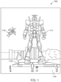
- FIG. 1 For example, referring to FIG. 1
- an augmented reality scene 1000 is depicted wherein a user of an AR technology sees a real-world park-like setting 1100 featuring people, trees, buildings in the background, and a concrete platform 1120.
- the user of the AR technology also perceives that he "sees" a robot statue 1110 standing upon the real-world platform 1120, and a cartoon-like avatar character 1130 flying by which seems to be a personification of a bumble bee, even though these elements do not exist in the real world.
- the human visual perception system is very complex, and producing a VR or AR technology that facilitates a comfortable, natural-feeling, rich presentation of virtual image elements amongst other virtual or real-world imagery elements is challenging.
- Systems and methods disclosed herein address various challenges related to VR and AR technology.
- waveguides and stacked waveguide assemblies that can be used in wearable display systems are described herein.
- An exemplary waveguide not according to the invention comprises an incoupling optical element, configured to incouple light at a first wavelength and to couple light out of the waveguide that is not at the first wavelength.
- the waveguide further comprises a wavelength selective region, where the wavelength selective region is configured to receive the incoupled light from the incoupling optical element and to propagate the incoupled light to a light distributing element.
- the wavelength selective region can be configured to attenuate the incoupled light not at the first wavelength relative to incoupled light at the first wavelength.
- the light distributing element can be configured to couple the incoupled light at the first wavelength out of the wavelength selective region.
- the waveguide also comprises an outcoupling optical element configured to receive the incoupled light at the first wavelength from the light distributing element and to couple the incoupled light at the first wavelength out of the waveguide.
- a method not according to the invention of displaying an optical image comprises incoupling light having a first wavelength and a second wavelength different from the first wavelength into a stacked waveguide assembly.
- the stacked waveguide assembly comprises a first waveguide and a second waveguide, wherein the first waveguide comprises a first layer of a wavelength selective region and a first layer of an outcoupling optical element.
- the second waveguide comprises a second layer of the wavelength selective region and a second layer of the outcoupling optical element.
- the method further comprises selectively attenuating the incoupled light at the second wavelength relative to the first wavelength in the first layer of the wavelength selective region and selectively attenuating the incoupled light at the first wavelength relative to the first wavelength in the second layer of the wavelength selective region.
- the method further comprises coupling the incoupled light at the first wavelength to the first layer of the outcoupling optical element and coupling the incoupled light at the first wavelength to the second layer of the outcoupling optical element.
- the method also comprises coupling the incoupled light at the first wavelength and the second wavelength out of the stacked waveguide assembly.
- Another example of a method not according to the invention of displaying an optical image comprises incoupling light having a first wavelength and a second wavelength different from the first wavelength into a waveguide and selectively attenuating the incoupled light at the second wavelength relative to the first wavelength in a first layer of a wavelength selective region.
- the method further comprises selectively attenuating the incoupled light at the first wavelength relative to the second wavelength in a second layer of the wavelength selective region and coupling the incoupled light at the first wavelength from a first light distributing element to a first layer of an outcoupling optical element.
- the method further comprises coupling the incoupled light at the second wavelength from a second light distributing element to a second layer of the outcoupling optical element and coupling the incoupled light at the first wavelength and second wavelength out of the outcoupling optical element.
- each point in the display's visual field it is desirable for each point in the display's visual field to generate the accommodative response corresponding to its virtual depth. If the accommodative response to a display point does not correspond to the virtual depth of that point, as determined by the binocular depth cues of convergence and stereopsis, the human eye may experience an accommodation conflict, resulting in unstable imaging, harmful eye strain, headaches, and, in the absence of accommodation information, almost a complete lack of surface depth.
- VR and AR experiences can be provided by display systems having displays in which images corresponding to a plurality of depth planes are provided to a viewer.
- the images may be different for each depth plane (e.g., provide slightly different presentations of a scene or object) and may be separately focused by the viewer's eyes, thereby helping to provide the user with depth cues based on the accommodation of the eye required to bring into focus different image features for the scene located on different depth plane and/or based on observing different image features on different depth planes being out of focus.
- depth cues provide credible perceptions of depth.
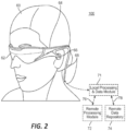
- FIG. 2 illustrates an example of wearable display system 100.
- the display system 100 includes a display 62, and various mechanical and electronic modules and systems to support the functioning of display 62.
- the display 62 may be coupled to a frame 64, which is wearable by a display system user, wearer, or viewer 60 and which is configured to position the display 62 in front of the eyes of the user 60.
- a speaker 66 is coupled to the frame 64 and positioned adjacent the ear canal of the user (in some embodiments, another speaker, not shown, is positioned adjacent the other ear canal of the user to provide for stereo/shapeable sound control).
- the display 62 is operatively coupled 68, such as by a wired lead or wireless connectivity, to a local data processing module 71 which may be mounted in a variety of configurations, such as fixedly attached to the frame 64, fixedly attached to a helmet or hat worn by the user, embedded in headphones, or otherwise removably attached to the user 60 (e.g., in a backpack-style configuration, in a belt-coupling style configuration).
- a local data processing module 71 which may be mounted in a variety of configurations, such as fixedly attached to the frame 64, fixedly attached to a helmet or hat worn by the user, embedded in headphones, or otherwise removably attached to the user 60 (e.g., in a backpack-style configuration, in a belt-coupling style configuration).
- the local processing and data module 71 may comprise a hardware processor, as well as digital memory, such as non-volatile memory (e.g., flash memory), both of which may be utilized to assist in the processing, caching, and storage of data.
- the data may include data a) captured from sensors (which may be, e.g., operatively coupled to the frame 64 or otherwise attached to the user 60), such as image capture devices (e.g., cameras), microphones, inertial measurement units, accelerometers, compasses, global positioning system (GPS) units, radio devices, and/or gyroscopes: and/or b) acquired and/or processed using remote processing module 72 and/or remote data repository 74, possibly for passage to the display 62 after such processing or retrieval.
- sensors which may be, e.g., operatively coupled to the frame 64 or otherwise attached to the user 60
- image capture devices e.g., cameras
- microphones e.g., inertial measurement units
- accelerometers compasses
- the local processing and data module 71 may be operatively coupled by communication links 76 and/or 78, such as via wired or wireless communication links, to the remote processing module 72 and/or remote data repository 74 such that these remote modules are available as resources to the local processing and data module 71.
- remote processing module 72 and remote data repository 74 may be operatively coupled to each other.
- the remote processing module 72 may comprise one or more processors configured to analyze and process data and/or image information.
- the remote data repository 74 may comprise a digital data storage facility, which may be available through the internet or other networking configuration in a "cloud" resource configuration. In some embodiments, all data is stored and all computations are performed in the local processing and data module, allowing fully autonomous use from a remote module.
- Vergence movements e.g., rotational movements of the pupils toward or away from each other to converge the lines of sight of the eyes to fixate upon an object
- vergence movements e.g., rotational movements of the pupils toward or away from each other to converge the lines of sight of the eyes to fixate upon an object
- accommodation movements e.g., rotational movements of the pupils toward or away from each other to converge the lines of sight of the eyes to fixate upon an object
- accommodation movements of the two eyes relative to each other are closely associated with focusing (or "accommodation") of the lenses of the eyes.
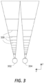
- FIG. 3 illustrates aspects of an approach for simulating three-dimensional imagery using multiple depth planes.
- objects at various distances from eyes 302 and 304 on the z-axis are accommodated by the eyes 302 and 304 so that those objects are in focus.
- the eyes 302 and 304 assume particular accommodated states to bring into focus objects at different distances along the z-axis. Consequently, a particular accommodated state may be said to be associated with a particular one of depth planes 306, with has an associated focal distance, such that objects or parts of objects in a particular depth plane are in focus when the eye is in the accommodated state for that depth plane.
- three-dimensional imagery may be simulated by providing different presentations of an image for each of the eyes 302 and 304, and also by providing different presentations of the image corresponding to each of the depth planes. While shown as being separate for clarity of illustration, the fields of view of the eyes 302 and 304 may overlap, for example, as distance along the z-axis increases. In addition, while shown as flat for ease of illustration, the contours of a depth plane may be curved in physical space, such that all features in a depth plane are in focus with the eye in a particular accommodated state. Without being limited by theory, it is believed that the human eye typically can interpret a finite number of depth planes to provide depth perception. Consequently, a highly believable simulation of perceived depth may be achieved by providing, to the eye, different presentations of an image corresponding to each of these limited number of depth planes.
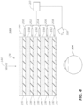
- FIG. 4 illustrates an example of a waveguide stack for outputting image information to a user.
- a display system 100 includes a stack of waveguides, or stacked waveguide assembly, 178 that may be utilized to provide three-dimensional perception to the eye/brain using a plurality of waveguides 182, 184, 186, 188, 190.
- the display system 100 shown in FIG. 4 may be used in the wearable display system 100 shown in FIG. 2 , with FIG. 4 schematically showing some parts of that system 100 in greater detail.
- the waveguide assembly 178 may be integrated into the display 62 of FIG. 2 .
- the waveguide assembly 178 may also include a plurality of features 198, 196, 194, 192 between the waveguides.
- the features 198, 196, 194, 192 may be lenses.
- the waveguides 182, 184, 186, 188, 190 and/or the plurality of lenses 198, 196, 194, 192 may be configured to send image information to the eye with various levels of wavefront curvature or light ray divergence. Each waveguide level may be associated with a particular depth plane and may be configured to output image information corresponding to that depth plane.
- Image injection devices 200, 202, 204, 206, 208 may be utilized to inject image information into the waveguides 182, 184, 186, 188, 190, each of which may be configured to distribute incoming light across each respective waveguide, for output toward the eye 304.
- Light exits an output surface of the image injection devices 200, 202, 204, 206, 208 and is injected into a corresponding input edge of the waveguides 182, 184, 186, 188, 190.
- a single beam of light (e.g., a collimated beam) is be injected into each waveguide to output an entire field of cloned collimated beams that are directed toward the eye 304 at particular angles (and amounts of divergence) corresponding to the depth plane associated with a particular waveguide.
- the image injection devices 200, 202, 204, 206, 208 are discrete displays that each produce image information for injection into a corresponding waveguide 182, 184, 186, 188, 190, respectively.
- the image injection devices 200, 202, 204, 206, 208 are the output ends of a single multiplexed display which may, e.g., pipe image information via one or more optical conduits (such as fiber optic cables) to each of the image injection devices 200, 202, 204, 206, 208.
- a controller 210 controls the operation of the stacked waveguide assembly 178 and the image injection devices 200, 202, 204, 206, 208.
- the controller 210 includes programming (e.g., instructions in a non-transitory computer-readable medium) that regulates the timing and provision of image information to the waveguides 182, 184, 186, 188, 190.
- the controller is be a single integral device (e.g., a hardware processor), or a distributed system connected by wired or wireless communication channels.
- the controller 210 is part of the processing modules 71 or 72 (illustrated in FIG. 2 ) in some embodiments.
- the waveguides 182, 184, 186, 188, 190 may be configured to propagate light within each respective waveguide by total internal reflection (TIR).
- the waveguides 182, 184, 186, 188, 190 may each be planar or have another shape (e.g., curved), with major top and bottom surfaces and edges extending between those major top and bottom surfaces.
- the waveguides 182, 184, 186, 188, 190 may each include light extracting optical elements 282, 284, 286, 288, 290 that are configured to extract light out of a waveguide by redirecting the light, propagating within each respective waveguide, out of the waveguide to output image information to the eye 304.
- Extracted light may also be referred to as outcoupled light, and light extracting optical elements may also be referred to as outcoupling optical elements.
- An extracted beam of light is outputted by the waveguide at locations at which the light propagating in the waveguide strikes a light redirecting element.
- the light extracting optical elements 82, 284, 286, 288, 290 may, for example, be reflective and/or diffractive optical features.
- the light extracting optical elements 282, 284, 286, 288, 290 are disposed at the top and/or bottom surfaces, and/or may be disposed directly in the volume of the waveguides 182, 184, 186, 188, 190.
- the light extracting optical elements 282, 284, 286, 288, 290 are formed in a layer of material that is attached to a transparent substrate to form the waveguides 182, 184, 186, 188, 190.
- the waveguides 182, 184, 186, 188, 190 are a monolithic piece of material and the light extracting optical elements 282, 284, 286, 288, 290 may be formed on a surface and/or in the interior of that piece of material.
- each waveguide 182, 184, 186, 188, 190 is configured to output light to form an image corresponding to a particular depth plane.
- the waveguide 182 nearest the eye may be configured to deliver collimated light, as injected into such waveguide 182, to the eye 304.
- the collimated light may be representative of the optical infinity focal plane.
- the next waveguide up 184 may be configured to send out collimated light which passes through the first lens 192 (e.g., a negative lens) before it can reach the eye 304.
- First lens 192 may be configured to create a slight convex wavefront curvature so that the eye/brain interprets light coming from that next waveguide up 184 as coming from a first focal plane closer inward toward the eye 304 from optical infinity.
- the third up waveguide 186 passes its output light through both the first lens 192 and second lens 194 before reaching the eye 304.
- the combined optical power of the first and second lenses 192 and 194 may be configured to create another incremental amount of wavefront curvature so that the eye/brain interprets light coming from the third waveguide 186 as coming from a second focal plane that is even closer inward toward the person from optical infinity than was light from the next waveguide up 184.
- the other waveguide layers e.g., waveguides 188, 190
- lenses e.g., lenses 196, 198
- the highest waveguide 190 in the stack sending its output through all of the lenses between it and the eye for an aggregate focal power representative of the closest focal plane to the person.
- a compensating lens layer 180 may be disposed at the top of the stack to compensate for the aggregate power of the lens stack 198, 196, 194, 192 below.
- Such a configuration provides as many perceived focal planes as there are available waveguide/lens pairings.
- Both the light extracting optical elements of the waveguides and the focusing aspects of the lenses may be static (e.g., not dynamic or electro-active). In some alternative embodiments, either or both are dynamic using electro-active features.
- the light extracting optical elements 282, 284, 286, 288, 290 may be configured to both redirect light out of their respective waveguides and to output this light with the appropriate amount of divergence or collimation for a particular depth plane associated with the waveguide.
- waveguides having different associated depth planes may have different configurations of light extracting optical elements, which output light with a different amount of divergence depending on the associated depth plane.
- the light extracting optical elements 282, 284, 286, 288, 290 are volumetric or surface features, which may be configured to output light at specific angles.
- the light extracting optical elements 282, 284, 286, 288, 290 may be volume holograms, surface holograms, and/or diffraction gratings.
- Light extracting optical elements, such as diffraction gratings, are described in U.S. Patent Publication No. 2015/0178939, published June 25, 2015 .
- the features 198, 196, 194, 192 are not lenses. Rather, they may simply be spacers (e.g., cladding layers and/or structures for forming air gaps).
- the light extracting optical elements 282, 284, 286, 288, 290 are diffractive features that form a diffraction pattern, or "diffractive optical element” (also referred to herein as a "DOE").
- the DOEs have a relatively low diffraction efficiency so that only a portion of the light of the beam is deflected (e.g., refracted, reflected, or diffracted) away toward the eye 304 with each intersection of the DOE, while the rest continues to move through a waveguide via total internal reflection.
- the light carrying the image information is thus divided into a number of related exit beams that exit the waveguide at a multiplicity of locations and the result is a fairly uniform pattern of exit emission toward the eye 304 for this particular collimated beam bouncing around within a waveguide.
- one or more DOEs are switchable between "on” states in which they actively diffract, and "off' states in which they do not significantly diffract.
- a switchable DOE may comprise a layer of polymer dispersed liquid crystal, in which microdroplets comprise a diffraction pattern in a host medium, and the refractive index of the microdroplets can be switched to substantially match the refractive index of the host material (in which case the pattern does not appreciably diffract incident light) or the microdroplet can be switched to an index that does not match that of the host medium (in which case the pattern actively diffracts incident light).
- the number and distribution of depth planes and/or depth of field can be varied dynamically based on the pupil sizes and/or orientations of the eyes of the viewer.
- a camera 500 e.g., a digital camera
- the camera 500 can be used to capture images of the eye 304 to determine the size and/or orientation of the pupil of the eye 304.
- the camera 500 can be used to obtain images for use in determining the direction the wearer 60 is looking (e.g., eye pose) or for biometric identification of the wearer (e.g., via iris identification).
- the camera 500 is attached to the frame 64 (as illustrated in FIG.
- the processing modules 71 and/or 72 may process image information from the camera 500 to determine, e.g., the pupil diameters and/or orientations of the eyes of the user 60.
- one camera 500 is utilized for each eye, to separately determine the pupil size and/or orientation of each eye, thereby allowing the presentation of image information to each eye to be dynamically tailored to that eye.
- the pupil diameter and/or orientation of only a single eye 304 is determined and assumed to be similar for both eyes of the viewer 60.
- depth of field may change inversely with a viewer's pupil size.
- the depth of field increases such that one plane not discernible because the location of that plane is beyond the depth of focus of the eye may become discernible and appear more in focus with reduction of pupil size and commensurate increase in depth of field.
- the number of spaced apart depth planes used to present different images to the viewer may be decreased with decreased pupil size. For example, a viewer may not be able to clearly perceive the details of both a first depth plane and a second depth plane at one pupil size without adjusting the accommodation of the eye away from one depth plane and to the other depth plane. These two depth planes may, however, be sufficiently in focus at the same time to the user at another pupil size without changing accommodation.
- the display system may vary the number of waveguides receiving image information based upon determinations of pupil size and/or orientation, or upon receiving electrical signals indicative of particular pupil sizes and/or orientations. For example, if the user's eyes are unable to distinguish between two depth planes associated with two waveguides, then the controller 210 may be configured or programmed to cease providing image information to one of these waveguides. Advantageously, this may reduce the processing burden on the system, thereby increasing the responsiveness of the system. In embodiments in which the DOEs for a waveguide are switchable between on and off states, the DOEs may be switched to the off state when the waveguide does receive image information.
- an exit beam may be desirable to have an exit beam meet the condition of having a diameter that is less than the diameter of the eye of a viewer.
- meeting this condition may be challenging in view of the variability in size of the viewer's pupils.
- this condition is met over a wide range of pupil sizes by varying the size of the exit beam in response to determinations of the size of the viewer's pupil. For example, as the pupil size decreases, the size of the exit beam may also decrease.
- the exit beam size may be varied using a variable aperture.
- FIG. 5 shows an example of exit beams outputted by a waveguide.
- One waveguide is illustrated, but other waveguides in the waveguide assembly 178 may function similarly, where the waveguide assembly 178 includes multiple waveguides.
- Light 400 is injected into the waveguide 182 at the input edge 382 of the waveguide 182 and propagates within the waveguide 182 by TIR. At points where the light 400 impinges on the DOE 282, a portion of the light exits the waveguide as exit beams 402.
- the exit beams 402 are illustrated as substantially parallel but they may also be redirected to propagate to the eye 304 at an angle (e.g., forming divergent exit beams), depending on the depth plane associated with the waveguide 182.
- Substantially parallel exit beams may be indicative of a waveguide with light extracting optical elements that outcouple light to form images that appear to be set on a depth plane at a large distance (e.g., optical infinity) from the eye 304.
- Other waveguides or other sets of light extracting optical elements may output an exit beam pattern that is more divergent, which would require the eye 304 to accommodate to a closer distance to bring it into focus on the retina and would be interpreted by the brain as light from a distance closer to the eye 304 than optical infinity.
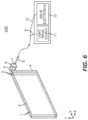
- FIG. 6 shows another example of the optical display system 100 including a waveguide apparatus, an optical coupler subsystem to optically couple light to or from the waveguide apparatus, and a control subsystem.
- the optical system 100 can be used to generate a multi-focal volumetric, image, or light field.
- the optical system can include one or more primary planar waveguides 1 (only one is shown in FIG. 6 ) and one or more DOEs 2 associated with each of at least some of the primary waveguides 1.
- the planar waveguides 1 can be similar to the waveguides 182, 184, 186, 188, 190 discussed with reference to FIG. 4 .
- the optical system may employ a distribution waveguide apparatus, to relay light along a first axis (vertical or Y-axis in view of FIG.
- the distribution waveguide apparatus may, for example include a distribution planar waveguide 3 and at least one DOE 4 (illustrated by double dash-dot line) associated with the distribution planar waveguide 3.
- the distribution planar waveguide 3 may be similar or identical in at least some respects to the primary planar waveguide 1, having a different orientation therefrom.
- the at least one DOE 4 may be similar or identical in at least some respects to the DOE 2.
- the distribution planar waveguide 3 and/or DOE 4 may be comprised of the same materials as the primary planar waveguide 1 and/or DOE 2, respectively.
- Embodiments of the optical display system 100 shown in FIGS. 4 or 6 can be integrated into the wearable display system 100 shown in FIG. 2 .
- the relayed and exit-pupil expanded light is optically coupled from the distribution waveguide apparatus into the one or more primary planar waveguides 10.
- the primary planar waveguide 1 relays light along a second axis, in some cases orthogonal to first axis, (e.g., horizontal or X-axis in view of FIG. 6 ).
- the second axis can be a non-orthogonal axis to the first axis.
- the primary planar waveguide 1 expands the light's effective exit pupil along that second axis (e.g., X-axis).
- the distribution planar waveguide 3 can relay and expand light along the vertical or Y-axis, and pass that light to the primary planar waveguide 1 which relays and expands light along the horizontal or X-axis.
- the optical system may include one or more sources of colored light (e.g., red, green, and blue laser light) 110 which may be optically coupled into a proximal end of a single mode optical fiber 9.
- a distal end of the optical fiber 9 may be threaded or received through a hollow tube 8 of piezoelectric material. The distal end protrudes from the tube 8 as fixed-free flexible cantilever 7.
- the piezoelectric tube 8 can be associated with 4 quadrant electrodes (not illustrated).
- the electrodes may, for example, be plated on the outside, outer surface or outer periphery or diameter of the tube 8.
- a core electrode (not illustrated) is also located in a core, center, inner periphery or inner diameter of the tube 8.
- Drive electronics 12 for example electrically coupled via wires 10, drive opposing pairs of electrodes to bend the piezoelectric tube 8 in two axes independently.
- the protruding distal tip of the optical fiber 7 has mechanical modes of resonance. The frequencies of resonance can depend upon a diameter, length, and material properties of the optical fiber 7. By vibrating the piezoelectric tube 8 near a first mode of mechanical resonance of the fiber cantilever 7, the fiber cantilever 7 is caused to vibrate, and can sweep through large deflections.
- the tip of the fiber cantilever 7 is scanned biaxially in an area filling two dimensional (2D) scan.
- 2D two dimensional
- a component of an optical coupler subsystem collimates the light emerging from the scanning fiber cantilever 7.
- the collimated light is reflected by mirrored surface 5 into the narrow distribution planar waveguide 3 which contains the at least one diffractive optical element (DOE) 4.
- the collimated light propagates vertically (relative to the view of FIG. 6 ) along the distribution planar waveguide 3 by total internal reflection, and in doing so repeatedly intersects with the DOE 4.
- the DOE 4 in some cases has a low diffraction efficiency.
- a fraction e.g. 10%
- the DOE 2 may advantageously be designed or configured to have a phase profile that is a summation of a linear diffraction pattern and a radially symmetric diffractive pattern, to produce both deflection and focusing of the light.
- the DOE 2 may advantageously have a low diffraction efficiency (e.g., 10%), so that only a portion of the light of the beam is deflected toward the eye of the view with each intersection of the DOE 2 while the rest of the light continues to propagate through the waveguide 1 via TIR.
- a low diffraction efficiency e.g. 10%
- the radially symmetric diffraction pattern of the DOE 2 additionally imparts a focus level to the diffracted light, both shaping the light wavefront (e.g., imparting a curvature) of the individual beam as well as steering the beam at an angle that matches the designed focus level.
- these different pathways can cause the light to be coupled out of the primary planar waveguide 1 by a multiplicity of DOEs 2 at different angles, focus levels, and/or yielding different fill patterns at the exit pupil.
- Different fill patterns at the exit pupil can be beneficially used to create a light field display with multiple depth planes.
- Each layer in the waveguide assembly or a stack of layers e.g., 3 layers
- a first stack of three adjacent layers may be employed to respectively produce red, blue and green light at a first focal depth.
- a second stack of three adjacent layers may be employed to respectively produce red, blue and green light at a second focal depth.
- Multiple stacks may be employed to generate a full 3D or 4D color image light field with various focal depths.
- the AR system may include other components in addition to the display system 100.
- the AR devices may, for example, include one or more haptic devices or components.
- the haptic device(s) or component(s) may be operable to provide a tactile sensation to a user.
- the haptic device(s) or component(s) may provide a tactile sensation of pressure and/or texture when touching virtual content (e.g., virtual objects, virtual tools, other virtual constructs).
- the tactile sensation may replicate a feel of a physical object which a virtual object represents, or may replicate a feel of an imagined object or character (e.g., a dragon) which the virtual content represents.
- haptic devices or components may be worn by the user (e.g., a user wearable glove).
- haptic devices or components may be held by the user.
- the AR system may, for example, include one or more physical objects which are manipulable by the user to allow input or interaction with the AR system. These physical objects are referred to herein as totems. Some totems may take the form of inanimate objects, for example a piece of metal or plastic, a wall, a surface of table. Alternatively, some totems may take the form of animate objects, for example a hand of the user. As described herein, the totems may not actually have any physical input structures (e.g., keys, triggers, joystick, trackball, rocker switch). Instead, the totem may simply provide a physical surface, and the AR system may render a user interface so as to appear to a user to be on one or more surfaces of the totem.
- the AR system may render an image of a computer keyboard and trackpad to appear to reside on one or more surfaces of a totem.
- the AR system may render a virtual computer keyboard and virtual trackpad to appear on a surface of a thin rectangular plate of aluminum which serves as a totem.
- the rectangular plate does not itself have any physical keys or trackpad or sensors.
- the AR system may detect user manipulation or interaction or touches with the rectangular plate as selections or inputs made via the virtual keyboard and/or virtual trackpad.
- FIG. 7A is a top view that schematically illustrates an example of a display 700 not according to the invention including a waveguide 905 that includes an incoupling optical element 1007, a light distributing element 1011, and an outcoupling optical element 1009.
- FIG. 7B schematically illustrates a cross-sectional view of the display 700 depicted in FIG. 7A along the axis A-A'.
- the waveguide 905 may be part of the stack of waveguides 178 in the display system 100 shown in FIG. 4 .
- the waveguide 905 may correspond to one of the waveguides 182, 184, 186, 188, 190
- the outcoupling optical element 1009 may correspond to the light extracting optical elements 282, 284, 286, 288, 290 of the display system 100.
- the display 700 is configured such that incoming incident light of different wavelengths represented by light rays 903i1, 903i2 and 903i3 (solid, dashed, and dash-double-dotted lines, respectively) are coupled into the waveguide 905 by the incoupling optical element 1007.
- the incoming incident light to the waveguide 905 can be projected from an image injection device (such as one of the image injection devices 200, 202, 204, 206, 208 illustrated in FIG. 4 ).
- the incoupling optical element 1007 can be configured to couple wavelengths of the incident light into the waveguide 905 at appropriate angles that support propagation through the waveguide 905 by virtue of total internal reflection (TIR).
- TIR total internal reflection
- a light distributing element 1011 can be disposed in the optical path along which the different wavelengths of light 903i1, 903i2 and 903i3 propagate through the waveguide 905.
- the light distributing element 1011 can be configured to redirect a portion of the light from the incoupling optical element 1007 toward the outcoupling optical element 1009, thereby enlarging the beam size of the interacting light along the direction of propagation. Accordingly, the light distributing element 1011 may be advantageous in enlarging the exit pupil of the display 700.
- the light distributing element 1011 may thus function as an orthogonal pupil expander (OPE).
- OPE orthogonal pupil expander
- the outcoupling optical element 1009 can be configured to redirect incoupled light that is incident on the element 1009 out of the x-y plane of the waveguide 905 at appropriate angles (e.g., in the z-direction) and efficiencies to facilitate proper overlay of light at different wavelengths and at different depth planes such that a viewer can perceive a color image of good visual quality.
- the outcoupling optical element 1009 can have an optical power that provides a divergence to the light that exits through the waveguide 905 such that the image formed by the light that exits through the waveguide 905 appears (to the viewer) to originate from a certain depth.
- the outcoupling optical element 1009 can enlarge the exit pupil of the display 700 and may be referred to as an exit pupil expander (EPE) that directs light to the viewer's eye.
- EPE exit pupil expander
- the incoupling optical element 1007, the outcoupling optical element 1009, and the light distributing element 1011 can each include one or more gratings, such as, for example, an analog surface relief grating (ASR), binary surface relief structures (BSR), volume holographic optical elements (VHOE), digital surface relief structures, and/or volume phase holographic material (e.g., holograms recorded in volume phase holographic material), or switchable diffractive optical elements (e.g., a polymer dispersed liquid crystal (PDLC) grating).
- ASR analog surface relief grating
- BSR binary surface relief structures
- VHOE volume holographic optical elements
- digital surface relief structures e.g., holograms recorded in volume phase holographic material
- switchable diffractive optical elements e.g., a polymer dispersed liquid crystal (PDLC) grating
- the incoupling optical element 1007 can include one or more optical prisms, or optical components including one or more diffractive elements and/or refractive elements.
- the various sets of diffractive or grating structures can be disposed on the waveguide by using fabrication methods such as injection compression molding, UV replication, or nano-imprinting of the diffractive structures.
- the incoupling optical element 1007, the outcoupling optical element 1009, or the light distributing element 1011 need not be a single element (e.g., as schematically depicted in FIGS. 7A, 7B , and 8 ) and each such element can include a plurality of such elements. These elements can be disposed on one (or both) of the surfaces 905a, 905b of the waveguide 905. In the example shown in FIGS. 7A, 7B , and 8 , the incoupling optical element 1007, the outcoupling optical element 1009, and the light distributing element 1011 are disposed on the surface 905a of the waveguide 905.
- the light distributing element 1011 can be disposed adjacent the first or the second surface 905a or 905b of the waveguide 905. In various embodiments, the light distributing element 1011 can be disposed such that it is spaced apart from the outcoupling optical element 1009, although the light distributing element 1011 need not be so configured in some embodiments.
- the light distributing element 1011 can be integrated with one or both of the first or the second surface 905a or 905b of the waveguide 905. In some embodiments, as disclosed herein, the light distributing element 1011 may be disposed in the bulk of waveguide 905.
- one or more wavelength selective filters may be integrated with or disposed adjacent to the incoupling optical element 1007, the outcoupling optical element 1009, or the light distributing element 1011.
- the display 700 illustrated in FIG. 7A includes the wavelength selective filter 1013, which is integrated into or on a surface of the waveguide 905.
- the wavelength selective filters can be configured to attenuate some portion of light at the one or more wavelengths that may be propagating along various directions in the waveguide 905.
- the wavelength selective filters can be absorptive filters such as color band absorbers or distributed switches (e.g., electro-optic materials).
- Light can be separated into constituent colors (e.g., red (R), green (G), and blue (B)), and it may be desirable to send different constituent colors to different layers of the waveguide assembly.
- each of the depth planes of the waveguide assembly may correspond to one or more layers to display particular colors of light (e.g., R, G, and B layers).
- a waveguide assembly having three depth planes, with each depth plane comprising three colors (e.g., R, G, and B), would include nine waveguide layers. Other numbers of depth planes and/or color layers per depth plane are available.
- the waveguide assembly can be configured to send light of the appropriate color to a particular layer in a particular depth plane (e.g., red light for a red color layer in a particular depth plane). It may be desirable if the light propagating in a particular color layer (e.g., a red layer) is substantially all in the desired color (e.g., red) with little admixture of other colors (e.g., blue or green) in that color layer.
- various implementations of the waveguide assembly can be configured to filter out undesired wavelengths of light in particular waveguide layers so that substantially only a single color (the desired color) propagates in that layer. Some such implementations may advantageously provide better color separation among the different color layers and lead to more accurate color representation by the display. Accordingly, color filters may be used to filter out the undesired constituent colors at different depth planes.
- the incoupling optical element 1007 includes two or more incoupling optical elements.
- light may be deflected by a first incoupling optical element into a first waveguide of a waveguide stack while other wavelengths may be transmitted to other layers of the incoupling optical element to be directed to other waveguides in the stack.
- the first layer of the incoupling optical element may be configured to deflect red light into the first waveguide (configured for red light) while transmitting other wavelengths (e.g., green and blue) to other layers of the waveguide stack.
- the incoupling optical elements may not always be perfectly configured to deflect all of the light at the given wavelength or transmit all of the light at the other wavelengths.
- the first layer of the incoupling optical element may be configured to deflect primarily red light
- physical limitations may inadvertently cause the first layer of the incoupling optical element to deflect an amount of other wavelengths (e.g., green and blue) into the first waveguide of the stack.
- some of the red light may be transmitted through the first layer of the incoupling optical element to other layers of the incoupling optical elements and be deflected into the associated waveguides (e.g., into green and blue waveguides).
- one or more portions of the waveguide stack can include a region that is configured to filter out or attenuate an unwanted wavelength or to isolate a desired wavelength.
- the first waveguide may be configured to propagate red light, so the waveguide may include a region (e.g., a tinted or dyed region) that is configured to attenuate the green and blue light in order to isolate the red light.
- the light distributing element 1011 includes (or is included in) the tinted or dyed region
- the region in and around the light distributing element 1011 may provide a greater volume than the incoupling optical element 1007 through which light may propagate.
- Providing the filtering functionality in the region of the light distributing element 1011 can allow the light manipulation action (e.g., filtering) to operate over a longer path length (which makes the filtering more effective) and/or reduce interferences along the primary optical path (e.g., the incoupling optical element 1007 and the outcoupling optical element 1009).
- FIG. 8 is a top view that schematically illustrates an example not according to the invention of a display 700 including a waveguide 905 that is generally similar to display shown in FIGS. 7A and 7B .
- the waveguide 906 includes the incoupling optical element 1007, the light distributing element 1011, and the outcoupling optical element 1009.
- the waveguide 905 also includes a wavelength selective region 924 that can selectively propagate certain wavelengths of light while selectively attenuating other wavelengths of light.
- the wavelength selective region can include a color filter.
- the wavelength selective region 924 can be disposed in and/or distributed through a region of the waveguide 905 in or around the light distributing element 1011.
- light received from the incoupling optical element 1007 can be selectively filtered by the wavelength selective region 924 before being propagated to the outcoupling optical element 1009.
- the wavelength selective region 924 represents a portion of the waveguide 905 that includes a distributed filter and/or switch material in at least some part.
- the wavelength selective region 924 includes a plurality of wavelength selective regions. As shown in the example in FIG. 8 , the wavelength selective region 924 represents the only portion of the optical path that includes a wavelength selective filter, such that, e.g., the incoupling optical element 1007 and the outcoupling optical element 1009 do not include wavelength selective filters. Because the light exiting the outcoupling optical element 1009 can include light from the world 144, the outcoupling optical element 1009 may not include a wavelength selective region so that the light from the world is not colored or tinted. Similarly, in order to maintain the composition of the incoming light into it, the incoupling optical element 1007 may optionally also not be selective for wavelength.
- the light distributing element 1011 may be advantageous to tint or dye layers of the light distributing element 1011 and not the incoupling optical element 1007 or the outcoupling optical element 1009. If the light is tinted before it enters the incoupling optical element 1007, this may attenuate the intensity of the incoupled light. If the incoupling optical element 1007 is tinted, the light may be coupled to the wrong waveguide. If the outcoupling optical element 1009 is tinted, light from the outside world that passes through the display 700 may be tinted or filtered, which may lead to distortions in the viewer's perception of the outside world. Each of these examples may be undesirable in certain designs.
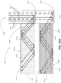
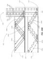
- FIG. 9 illustrates a perspective view of an example stack 1200 of waveguides not according to the invention.
- the view along the axis A-A' in FIG. 9 is generally similar to the view shown in FIG. 7B .
- the stack 1200 of waveguides includes waveguides 1210, 1220, and 1230.
- the layers of a light distributing element 1210, 1220, 1230 can correspond to the light distributing element 1011 in FIG. 8 .
- each waveguide can include an associated layer of the incoupling optical element, with, e.g., the layer of the incoupling optical element 1212 disposed on a surface (e.g., a bottom surface) of the waveguide 1210, the layer of the incoupling optical element 1224 disposed on a surface (e.g., a bottom surface) of the waveguide 1220, and the layer of the incoupling optical element 1232 disposed on a surface (e.g., a bottom surface) of the waveguide 1230.
- the layer of the incoupling optical element 1212 disposed on a surface (e.g., a bottom surface) of the waveguide 1210
- the layer of the incoupling optical element 1224 disposed on a surface (e.g., a bottom surface) of the waveguide 1220
- the layer of the incoupling optical element 1232 disposed on a surface (e.g., a bottom surface) of the waveguide 1230.
- One or more of the layers of the incoupling optical element 1212, 1222, 1232 may be disposed on the top surface of the respective waveguide 1210, 1220, 1230 (particularly where the one or more layers of the incoupling optical element are optically transmissive and/or deflective). Similarly, the other incoupling optical elements 1222, 1232 may be disposed on the bottom surface of their respective waveguide 1220, 1230 (or on the top surface of the next lower waveguide). In some designs, the layers of the incoupling optical element 1212, 1222, 1232 are disposed in the volume of the respective waveguide 1210, 1220, 1230.
- the incoupling optical elements 1212, 1222, 1232 may include a wavelength selective filter, such as a filter that selectively reflects, refracts, transmits, and/or diffracts one or more wavelengths of light, while transmitting, diffracting, refracting, and/or reflecting other wavelengths of light.
- a wavelength selective filter such as a filter that selectively reflects, refracts, transmits, and/or diffracts one or more wavelengths of light, while transmitting, diffracting, refracting, and/or reflecting other wavelengths of light.
- wavelength selective filters include color filters such as dyes, tints, or stains.
- the wavelength selective filter can include a dichroic filter, a Bragg grating, or a polarizer.
- the wavelength selective filter may include a bandpass filter, a shortpass filter, or a longpass filter.
- the layers of the incoupling optical element 1212, 1222, 1232 may be disposed in other areas of their respective waveguide 1210, 1220, 1230 in other embodiments.
- the waveguides 1210, 1220, 1230 may be spaced apart and separated by gas (e.g., air), liquid, and/or solid layers of material.
- light rays 1240, 1242, 1244 are incident on the stack 1200 of waveguides.
- the stack 1200 of waveguides may be part of the stack of waveguides in the display system 100 ( FIG. 4 ).
- the waveguides 1210, 1220, 1230 may correspond to three of the waveguides 182, 184, 186, 188, 190, and the light rays 1240, 1242, 1244 may be injected into the waveguides 1210, 1220, 1230 by one or more image injection devices 200, 202, 204, 206, 208.
- the light rays 1240, 1242, 1244 have different properties, e.g., different wavelengths or ranges of wavelengths, which may correspond to different colors.
- the layers of the incoupling optical element 1212, 122, 1232 can be configured to selectively deflect the light rays 1240, 1242, 1244 based upon a particular feature of the property of light, (e.g., wavelength, polarization) while transmitting light that does not have that property or feature.
- the layers of the incoupling optical element 1212, 122, 1232 each selectively deflect one or more particular wavelengths of light, while transmitting other wavelengths.
- the non-deflected light may propagate into a different waveguide and/or waveguide layer.
- the layer of the incoupling optical element 1212 may be configured to selectively deflect a light ray 1240, which has a first wavelength or range of wavelengths, while transmitting the light rays 1242 and 1244, which have different second and third wavelengths or ranges of wavelengths, respectively.
- the deflected light rays 1240, 1242, 1244 are deflected so that they propagate through the corresponding waveguide 1210, 1220, 1230; that is, the layers of the incoupling optical element 1212, 1222, 1232 of each respective waveguide couple (e.g., deflect) light into the corresponding waveguide 1210, 1220, 1230.
- the light rays 1240, 1242, 1244 are deflected at angles that cause the light to propagate through the respective waveguide 1210, 1220, 1230 (e.g., by TIR).
- the light rays 1240, 1242, 1244 are incident on the corresponding layer of the light distributing element 1214, 1224, 1234.
- the layers of the light distributing element 1214, 1224, 1234 deflect the light rays 1240, 1242, 1244 so that they propagate towards the corresponding layer of the outcoupling optical element 1250, 1252, 1254.
- an angle-modifying optical element 1260 may be provided to alter the angle at which the light rays 1240, 1242, 1244 strike the layers of the incoupling optical element.
- the angle-modifying optical element can cause the light rays 1240, 1242, 1244 to impinge on the corresponding layer of the incoupling optical element 1212, 1222, 1232 at angles appropriate for TIR.
- the light rays 1240, 1242, 1244 may be incident on the angle-modifying optical element 1260 at an angle normal to the waveguide 1210.
- the angle-modifying optical element 1260 then changes the direction of propagation of the light rays 1240, 1242, 1244 so that they strike the layers of the incoupling optical elements 1212, 1222, 1232 at an angle of less than 90 degrees relative to the surface of waveguide 1210.
- the angle-modifying optical element 1260 may include a grating, a prism, and/or a mirror.
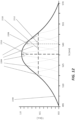
- FIG. 10A is a side view that schematically illustrates an example display according to the invention where two waveguides 1210, 1220 of the light distributing element 1011 include color filters 1060a, 1060b.
- the number of waveguides in a given embodiment of the light distributing element 1011 could be greater or fewer than two.
- the incoming light beam 1360 e.g., white light
- the incoming light beam 1360 may include multiple wavelengths 1354, 1358 of light (represented by different dashing patterns in FIG. 10A ), which may comprise wavelengths ⁇ 1 and ⁇ 2.
- the number of constituent light beams may be greater or fewer than two.
- ⁇ 1 and ⁇ 2 may represent different colors of light that are being injected into the display (e.g., blue and green). Any combination of colors can be described by ⁇ 1 and ⁇ 2.
- the incoming light beam 1360 can comprise visible light, or in various implementations, non-visible light such as infrared or ultraviolet light.
- the waveguides 1210, 1220 include color filters 1060a, 1060b.
- Each waveguide 1210, 1220 may be associated with a particular design wavelength. This can mean that a waveguide that is associated with a design wavelength includes an incoupling optical element that is configured to deflect light at the design wavelength to an associated layer of the light distributing element and/or that the associated wavelength selective region is configured to attenuate light not at the design wavelength.
- the first waveguide 1210 may have ⁇ 1 as a design wavelength
- the second waveguide 1220 may have ⁇ 2 as a design wavelength.
- the first layer of the incoupling optical element 1212 would be configured to deflect ⁇ 1 to the first layer of the light distributing element 1214
- the second layer of the incoupling optical element 1222 would be configured to deflect ⁇ 2 to the second layer of the light distributing element 1224.
- the color filters 1060a, 1060b can be designed or tuned to purify or isolate a desired wavelength or set of wavelengths for the corresponding waveguide 1210, 1220. Alternatively, the color filters 1060a, 1060b can attenuate undesired wavelengths.
- the first color filter 1060a may include a tint that attenuates red light.
- the second color filter 1060b may include a tint that attenuates green light.
- the color filters 1060a, 1060b can optionally be electronically switchable so that they attenuate light when they are switched on and do not attenuate light when switched off. Examples of color filters include materials that are dyed, tinted, or stained. Color filters may optionally include a dichroic filter or a Bragg grating.
- references to a given color of light throughout this disclosure will be understood to encompass light of one or more wavelengths within a range of wavelengths of light that are perceived by a viewer as being of that given color.
- red light may include light of one or more wavelengths in the range of about 620-780 nm
- green light may include light of one or more wavelengths in the range of about 492-577 nm
- blue light may include light of one or more wavelengths in the range of about 435-493 nm.
- the waveguides described herein can be configured to operate on wavelength bands outside the visual, e.g., infrared or ultraviolet.
- the term "a wavelength” should be understood to mean “a single wavelength” or "a range of wavelengths” in various implementations.
- the wavelength represented by ⁇ 1 may represent blue light, which may include light of one or more wavelengths in the range of about 450-470nm.
- each waveguide 1210, 1220 may be associated with a particular color filter 1060a, 1060b.
- the first constituent light beam 1354 is deflected (e.g., refracted, reflected, or diffracted) at least in part due to its wavelength ⁇ 1.
- an undeflected first constituent light beam 1354b may be transmitted through the first layer of the incoupling optical element 1212 at least in part due to its ⁇ 1 not being fully optically interactive with the first layer of the incoupling optical element 1212.
- a second constituent light beam 1358 is transmitted at least in part due to its wavelength ⁇ 2.
- an amount of an untransmitted second constituent light beam 1358b may deflect off the first layer of the incoupling optical element 1212 at least in part due to its ⁇ 2 being optically interactive with the first layer of the incoupling optical element 1212.
- a first resultant light beam 1360a includes a first target light beam 1354a, which is at the design wavelength for the first waveguide 1210, and the untransmitted second constituent light beam 1358b, which is not at the design wavelength for the first waveguide.
- the first waveguide 1210 in order to attenuate the intensity of the untransmitted second constituent light beam 1358b, the first waveguide 1210 includes a first color filter 1060a as described herein. Due at least in part to the first color filter 1060a, as schematically depicted in FIG. 10A , the intensity of the untransmitted second constituent light beam 1358b may be attenuated as it propagates through the first waveguide 1210.
- the intensity of the untransmitted second constituent light beam 1358b is attenuated relative to the first target light beam 1354a.
- the first layer of the light distributing element 1214 can be configured to deflect the first target light beam 1354a to an associated layer of the outcoupling optical element (not shown).
- a second resultant light beam 1360b may include a second target light beam 1358a, which is at the design wavelength for the second waveguide 1220, and the undeflected first constituent light beam 1354b, which is not at the design wavelength for the second waveguide 1220.
- the first waveguide 1210 in order to attenuate the intensity of the undeflected first constituent light beam 1354b, the first waveguide 1210 includes a second color filter 1060b as described herein. Due at least in part to the second color filter 1060b, as schematically depicted in FIG. 10A , the intensity of the undeflected first constituent light beam 1354b can be attenuated as it propagates through the second waveguide 1220.
- the intensity of the undeflected first constituent light beam 1354b is attenuated relative to the second target light beam 1358a.
- the second layer of the light distributing element 1224 can be configured to deflect the second target light beam 1358a to an associated layer of the outcoupling optical element (not shown).
- the light 1360 may enter the waveguide stack and be coupled into a proximal surface of the first waveguide 1210.
- the first layer of the incoupling optical element 1212 may be disposed on a distal surface of the first waveguide 1210 and/or on a proximal surface of the second waveguide 1220. In some designs, the first layer of the incoupling optical element 1212 is disposed within the volume of the first waveguide 1210.
- the first layer of the incoupling optical element may be disposed parallel to one or both of the proximal and distal surfaces of the first waveguide 1210. As shown, the proximal surface and the distal surface of the first waveguide are parallel to one another. In some configurations, the proximal surface may not be parallel to the distal surface.
- the first layer of the incoupling optical element 1212 may be disposed at an angle relative to the distal surface and/or proximal surface of the first waveguide 1210.
- FIG. 10B schematically illustrates a side view of an example display where two waveguides 1210, 1220 include distributed switch materials 1070a, 1070b.
- the number of waveguides in a given embodiment could be greater or fewer than two.
- the waveguides 1210, 1220 include distributed filter and/or switch material, such as switch materials 1070a, 1070b.
- switch materials include dichroic filters, electronically switchable glass, and electronically switchable mirrors.
- the switch materials 1070a, 1070b can be electronically switched to modify, e.g., the brightness, polarization, angle of reflection, or angle of refraction of light.
- Some switch materials may also include electrochromic, photochromic, thermochromic, suspended particle, or micro-blind materials, or polymer dispersed liquid crystals.
- electrochromic elements may be used to modify the brightness and/or intensity of light.
- a polymer dispersed liquid crystal grating or other tunable grating may be used to modify an angle at which light is propagated through the waveguide.
- the switch materials can be designed or tuned to attenuate light of unwanted colors or wavelengths.
- the first switch material 1070a may include a filter that attenuates blue light by disrupting the propagation of blue light.
- the first switch material 1070a can include a filter that attenuates colors of light that are not blue by disrupting the propagation of the light at those wavelengths.
- the switch materials 1070a, 1070b are electronically switchable to attenuate light when they are switched on and not attenuate light when switched off.
- the propagation of light may be disrupted, for example, by causing the light to become absorbed, by altering the index of refraction of the material in a way that prevents the light from propagating by total internal reflection, and/or by substantially altering the path angle of the light.
- a first switch material 1070a may be disposed as a layer on a distal surface of the first waveguide 1210, as shown in FIG. 10B , and/or on a proximal surface of the second waveguide 1220 (e.g., in a stacked waveguide configuration). In some designs, the first switch material 1070a is disposed on a proximal surface of the first waveguide 1210. As shown, the first switch material 1070a may be disposed parallel to the proximal surface of the waveguide. In some designs, the first switch material 1070a is oriented at an angle relative to the distal and/or proximal surface of the waveguide 1210. The first switch material 1070a may be disposed within the volume of the first waveguide 1210.
- the switch material may disposed along a plane intersecting one or more surfaces of the first waveguide 1210 and/or or may be disposed volumetrically (e.g., throughout the whole volume) in the first waveguide material (e.g., mixed and/or patterned into the first waveguide material).
- the first switch material 1070a may include a material that alters the index of refraction and/or absorption of light for certain ranges of wavelengths.
- the first switch material may be disposed along a plane perpendicular to entering light rays 1360 and/or parallel to the first layer of the incoupling optical element 1212.
- the first switch material is disposed along two or more surfaces of the first waveguide 1210, such as, for example, adjacent surfaces and/or opposite surfaces (e.g., proximal and distal surfaces).
- Distributed switch materials may be used to steer a beam (e.g., before being outcoupled by the outcoupling optical element). Beam steering may allow expanding the field of view of a user.
- a polymer dispersed liquid crystal grating or other tunable grating may be implemented as distributed switch materials and used to perform beam steering by modifying an angle of TIR waveguided light, an angle at which light is outcoupled by the outcoupling optical element, or a combination thereof.
- Switch materials can be used to modulate light received from upstream components (e.g., light source, LCoS). Different waveguides or layers of the light distributing element may be independently electronically switched (e.g., by the controller 210).
- modulation processes that are typically performed by the upstream components can be performed at the waveguide stack through strategic control of the distributed switches. Accordingly, outcoupling can be enabled or disabled on a waveguide-by-waveguide basis by controlling the associated distributed switches.
- one or more metasurfaces may be used for beam control (e.g., beam steering). Further information on metasurfaces and metamaterials that may be used as distributed switch materials in various embodiments of this disclosure can be found in U.S. Patent Publication No. 2017/0010466 and/or U.S. Patent Publication No. 2017/0010488 .
- FIG. 11 illustrates a schematic of an example waveguide 1210 with multiple filter regions 1104.
- the filter regions 1104 may be color filters and/or switch materials. Additional wavelength selective filters may also be present in the waveguide 1210.
- the filter regions 1104 can include any volumetric optical filters as described herein.
- the wavelengths that comprise a light beam can be filtered into a series of waveguides through wavelength multiplexing.
- Wavelength multiplexing can allow images to be sent to different waveguides simultaneously, e.g., by using or modulating laser diodes at different wavelengths simultaneously. This can result in a simple switching method that addresses different display waveguides. It can enable a rich light field where photons appear to arrive from different depth planes simultaneously.
- each waveguide in the display can correspond to a particular depth plane of an image.
- each depth plane can be associated with a stack of waveguides configured to display different colors.
- each depth plane may include a stack of three waveguides associated with red (R) light, green (G) light, and blue (B) light. To achieve this, it may be desirable to split light into separate colors (e.g., red, green, blue) as well as into subcolors.
- Subcolors refer to wavelengths or ranges of wavelengths falling substantially within the range of wavelengths encompassed by the associated color.
- the green color may span the range of wavelengths from about 495 nm to 570 nm.
- the human eye tends to identify as green those wavelengths that contain primarily wavelengths in that range.
- a green subcolor could include a range of wavelengths from 500 nm to 510 nm, from 525 nm to 560 nm, from 555 nm to 560 nm, etc. Humans may see substantially the same color when they view subcolors whose peak intensities are near each other.
- Subcolors, within a color have wavelength subranges that are within the wavelength range of the color, and different subcolors have different wavelength subranges that may, or may not, at least partially overlap in wavelength.
- FIG. 12 illustrates an example of a series of subcolors 2204 within a color 2200.
- the color 2200 spans wavelengths of approximately 495 nm to 570 nm.
- this color represents a source of green light with a peak intensity at about 530 nm.
- the shape and dimensions of the intensity profile for this color is merely an example, and it may take on other shapes and dimensions.
- Subcolors 2204 of the color 2200 illustrate examples of other intensity profiles that may still be considered "green” to human observers.
- the width 2212 of the curve of each subcolor 2204 is narrower than that of the color 2200.
- Each subcolor 2204 can have a width 2212 and a peak wavelength 2208, but for clarity the width 2212 and peak wavelength 2208 are not labeled for each subcolor.
- the width 2212 of each subcolor can be represented by, e.g., the full width at half maximum (FWHM).
- the distance between peak wavelengths 2208 of each subcolor 2204 can be between about 1-120 nm. In some embodiments, the distance between peak wavelengths can be in a range of about 10-80 nm.
- the distance between peak wavelengths can be between about 15-50 nm.
- the width 2212 of each subcolor 2204 can be between about 3-35 nm, between about 5-55 nm, less than 20 nm, less than 30 nm, less than 40 nm, or some other width.
- the number and widths of subcolors can be selected based on the multiplexing properties of the display device.
- the color 2200 approximates a Gaussian curve, though other curves and beam profiles are possible.
- the color 2200 can be described by its peak wavelength 2216 and width 2220 (e.g., a full-width at half maximum (FWHM)).
- the width 2216 can vary according to different embodiments.
- the width 2216 can range between about 40-220 nm.
- the width can range between about 15-120 nm, between about 60-160, between about 45-135 nm, less than 10 nm, or greater than 175 nm.
- the ratio of the width 2216 of a color to the width 2208 of a subcolor can be in a range from about 2 to 5. In some embodiments, this ratio can be between about 4-12, between about 10-25, be less than 2, or be greater than 25.
- references to a given color or color of light throughout this disclosure encompass light of one or more wavelengths within a range of wavelengths of light that are perceived by a viewer as being of that given color.
- red light may include light of one or more wavelengths in the range of about 620-780 nm
- green light may include light of one or more wavelengths in the range of about 495-570 nm
- blue light may include light of one or more wavelengths in the range of about 435-495 nm.
- the waveguides described herein can be configured to operate on wavelength bands outside the visual, e.g., infrared or ultraviolet.
- the term "wavelength" can mean "a single wavelength” or "a range of wavelengths" in various implementations.
- FIG. 13 schematically illustrates a side view of an example stacked waveguide assembly 178.
- FIG. 13 shows two waveguide stacks 960a, 960b. There can be more than two waveguide stacks in other implementations. As shown in FIG. 13 , each waveguide stack 960a, 960b includes three waveguides, but the waveguide stacks 960a, 960b may comprise one, two, four, or more waveguides and is not limited by the illustration in FIG. 13 . Each waveguide stack 960a, 960b may produce a different depth plane 306, as shown in FIG. 3 .
- the waveguide stacks 960a, 960b may each be associated with a particular depth plane in a light field display.
- the waveguide stack 960a may be used to display images perceivable at a first distance from the wearer
- the waveguide stack 960b may be used to display images perceivable at a second distance from the wearer, where the second distance is different from the first distance.
- Each waveguide stack 960a, 960b can be designed to display one or more colors. In the example shown in FIG. 13 , each stack 960a, 960b includes three waveguides for three different colors (e.g., red, green, and blue).
- each waveguide stack may be associated with particular subcolors.
- the first waveguide stack 960a may be associated with a first subcolor of three different colors, e.g., blue, green, and red.
- a first pair of light rays 952a, 952b can represent two subcolors of the same color.
- the first pair of light rays 952a, 952b may represent light at two subcolors of blue, such as 440 nm and 450 nm light.
- Each waveguide in the stacked waveguide assembly 178 can be configured to receive light at a particular design wavelength. Generally, the design wavelength corresponds to a particular subcolor. As illustrated in FIG. 13 , each waveguide 962a, 966a, 968a, 962b, 966b, 968b can comprise a corresponding incoupling optical element 1007a, 1007b, 1007c, 1007d, 1007e, 1007f.
- the incoupling optical element 1007 comprises the incoupling optical elements 1007a, 1007b, 1007c, 1007d, 1007e, 1007f.
- Each incoupling optical element 1007a, 1007b, 1007c, 1007d, 1007e, 1007f can be configured to deflect a design wavelength into the corresponding waveguide 962a, 966a, 968a, 962b, 966b, 968b.
- the display may attempt to show a blue object that is at a particular depth from the viewer of the display.
- rays 952a and 952b may represent the propagation of blue light. If a fraction of the blue light (e.g., the ray 952a) that should be displayed at a first depth plane (e.g., 960a) is misdirected to a different depth plane (e.g., 960b), then the resulting image displayed to a viewer of the waveguide 905 will not accurately reflect the depth of the blue object in the image.
- a fraction of the blue light that should be displayed at a blue color layer (e.g., layer 962a) in the waveguide stack 960a is misdirected to a red or green layer (e.g., layers 966a, 968a), then the color of the blue object will not be accurately displayed to the viewer.
- a red or green layer e.g., layers 966a, 968a
- diffraction gratings which may be used to diffract the light from an incident direction (e.g., downward as shown in FIG. 13 ) to a propagation direction in the waveguide layer (e.g., horizontal as shown in FIG. 13 ), are not 100% efficient.
- optical gratings often diffract light having wavelengths across a broad spectrum and may affect light of wavelengths that were not intended.
- gratings tuned to diffract light of one color e.g., red
- may diffract light of other colors e.g., blue or green. Therefore, for example, a small fraction of the light in the ray 952a, which should be directed by the incoupling optical element 1007a into the layer 926a, may pass through the incoupling optical element 1007a and be directed into one (or more) of the other layers of the waveguide. Similar considerations apply for green or red light input into the incoupling optical element 1007.
- certain embodiments of the display use a wavelength multiplexing technique to direct light to the appropriate layer in the waveguide.
- the wavelengths used for blue light rays 952a and 952b may be slightly different from each other and represent different subcolors of the color blue.
- the wavelengths used for green light rays 956a and 956b may be slightly different from each other and represent different subcolors of the color green.
- the wavelengths used for red light rays 958a and 958b may be slightly different from each other and represent different subcolors of the color red.
- the incoupling optical elements 1007a-1007f can be configured to strongly re-direct light of the appropriate wavelength into the corresponding layer in the waveguide assembly. Light that passes through the incoupling element will have a much lower likelihood of being misdirected by a different incoupling element, because the different element is configured to re-direct a different range of wavelengths.
- the blue light ray 952a can be centered at a range of wavelengths around 435 nm (e.g., a first blue subcolor), while the blue light ray 952b can be centered at a different range of wavelengths around 445 nm (e.g., a second blue subcolor).
- the incoupling optical element 1007a can be configured to re-direct blue light of the first blue subcolor, while the incoupling optical element 1007d can be configured to re-direct blue light of the second blue subcolor.
- the blue light ray 952a is preferentially re-directed into the layer 962a
- the blue light ray 952b is preferentially re-directed into the layer 962b.
- Similar considerations apply to the use of different green subcolors for the green light rays 956a, 956b and different red subcolors for the red light rays 958a, 958b.
- the foregoing is merely an example, and as shown in FIG. 12 , many different subcolors of a particular color can be used to multiplex light of that color into the appropriate layers of the waveguide 905.
- the width of the wavelength range of a subcolor can be selected so that the incoupling optical element can efficiently redirect the subcolor into the appropriate layer.
- the properties of the incoupling optical element e.g., a diffractive grating period
- the first waveguide stack 960a can couple a first subcolor of three colors, such as blue, green, and red.
- the second waveguide stack 960b can couple a second subcolor of the three colors.
- the first waveguides 962a, 962b of each stack can be configured to receive the first and second subcolors of a first color, such as blue.
- the second waveguides 966a, 966b of each stack can be configured to receive the first and second subcolors of a second color, such as green.
- subcolors of the same color may propagate through adjacent waveguides.
- Such waveguides may form a waveguide stack dedicated to a particular color.
- a first waveguide may have a first subcolor of blue as a design wavelength and a second waveguide may have a second subcolor of blue as the design wavelength.
- a third waveguide may have a first subcolor of a second color (e.g., green).
- subcolors of a first wavelength e.g., blue
- subcolors of a second wavelength e.g., green
- the number of waveguide stacks can be greater than two, and the number of waveguides within each waveguide stack can be two or greater.
- Three design wavelength waveguides per waveguide stack are illustrated in FIG. 13 as an example of where one color of each of three primary colors, such as blue, green, and red, are incoupled within each waveguide stack. However, this is not intended to limit the number of waveguides, waveguide stacks, or types of colors that can be incoupled.
- the light at the color of the corresponding wavelength is incoupled into the corresponding design wavelength waveguide and out of the incoupling optical element 980, the light propagates through the corresponding waveguide 962a, 966a, 968a, 962b, 966b, 968b.
- a corresponding light distributing element 1011a, 1011b, 1011c, 1011d, 1011e, 1011f can deflect the light at the corresponding design wavelength to a corresponding layer of the outcoupling optical element (not shown).
- the corresponding layer of the outcoupling optical element is configured to couple the light at the corresponding design out of the stacked waveguide assembly.
- FIG. 14 schematically illustrates a side view of an example stacked waveguide assembly 178 with a preliminary light filter system 1080.
- the preliminary light filter 1080 can be used to provide a first-order color selection process.
- the preliminary light filter system 1080 can comprise a number of optical elements 1084a, 1084b, 1088a, 1088b, such as gratings, mirrors, prisms, and other refractive and/or reflective elements.
- the filter system 1080 may include diffractive optical elements as well. The precise number and configuration of the optical elements is shown here by way of example only and may be changed as necessary.
- the filter system 1080 can be used to direct light of different wavelengths to different color layers or depth planes of the waveguide 905.
- a wavelength multiplexing waveguide assembly can include one or more wavelength selective filters.
- FIG. 15A shows the waveguide assembly 178 of FIG. 13 with distributed filters 1502a, 1502b, 1502c, 1502d, 1502e, 1502f.
- the distributed filters can include any optical filter described herein, such, for example, an absorptive filter, a refractive filter, a diffractive filter, and/or a reflective filter.
- the optical filter may be a color filter (e.g., selecting for a specific range of wavelengths). Examples of absorptive filters include tints, dyes, or stains.
- Refractive filters include optical elements that filter based on different indices of refraction for different wavelengths of light.
- diffractive filters include gratings.
- reflective filters include dichroic mirrors.
- the optical filter may include a polarizer.
- the waveguides 962a-968a (and the waveguides 962b-968b) can perform color (or subcolor) filtering as described with reference to FIG. 10A .
- the incoupling optical element 1007 may perform less wavelength filtering in such embodiments, because the corresponding waveguides include a distributed filter that can provide some or all of the wavelength filtering.
- FIG. 15B shows the waveguide assembly 178 of FIG. 13 with distributed switches 1506a, 1506b, 1506c, 1506d, 1506e, 1506f.
- the distributed switches may include any filter described herein.
- Distributed switches may include an electrically switchable layer and/or an electrically switchable volume. Examples of electrically switchable materials include switchable dichroics, switchable mirrors, switchable gratings, switchable holograms, switchable glasses, and switchable polarizers.
- the distributed switches may include polymer dispersed liquid crystal or other liquid crystal assemblies (e.g., liquid crystal on silicon (LCoS)).
- LCDoS liquid crystal on silicon
- the switchable material can be switched to alter a reflective, absorptive, refractive, diffractive, and/or polarizing quality of the material.
- an electrical signal may cause the material to attenuate (e.g., absorb, deflect away) red light while propagating blue light (e.g., via TIR).
- a polarizer may be configured to turn on or off based on an electrical signal.
- a polarizer may include a cholesteric liquid crystal element. Other configurations are also possible.
- distributed switches 1506a, 1506b, 1506c, 1506d, 1506e, 1506f may be disposed along a surface of corresponding waveguides 962a, 966a, 968a, 962b, 966b, 968b.
- a surface may be a distal surface from the incoming light 1360 as shown in FIG. 15B , but other surfaces (e.g., a proximal surface to the light 1360, a surface perpendicular to the proximal surface) are also possible.
- the switchable material is disposed throughout the volume (e.g., volumetrically) of the corresponding waveguides.
- a switchable layer may be disposed within the corresponding waveguide along a plane that is not parallel to any surface of the waveguide.
- a switchable material may be disposed on a layer not coplanar with a surface of the waveguide.
- the waveguide assembly 178 can include a combination of both distributed filters 1502a-1502f and distributed switches 1506a-1506f.
- Waveguide assemblies 178 such as the examples shown in FIGS. 15A and 15B can utilize the distributed filters 1502a-1502f or the distributed switches 1506a-1506f to perform subcolor filtering within one or more waveguides 962a-968b.
- the incoupling optical element 1007 may be less wavelength selective than in the waveguide assembly embodiments 178 that use only one or the other of distributed filtering or distributed switching, which advantageously may reduce degradation along the optical path that passes through each waveguide in the stack.
- FIG. 16 is an International Commission on Illumination (CIE) chromaticity diagram 1100 with x-y axes (e.g., normalized tristimulus values) describing the hypothetical human visual response gamut 1152 at which colors are perceived.
- CIE International Commission on Illumination
- Each waveguide stack 960a, 960b can represent colors in a corresponding color gamut, 1160a, 1160b, which is typically smaller than the entire gamut 1152 of all perceivable colors.
- the vertices of each gamut 1160a, 1160b correspond to the colors of the corresponding waveguides in each stack.
- the gamut 1160a for the waveguide stack 960a has vertices corresponding to the colors propagated by the waveguides 962a, 966a, and 968a
- the gamut 1160b for the waveguide stack 960b has vertices corresponding to the colors propagated by the waveguides 962b, 966b, and 968b.
- Each gamut 1160a, 1160b has an associated white point 1192a, 1192b (near the center of each gamut) that represents the chromaticity of white.
- the gamuts 1160a, 1160b substantially overlap so that each of the waveguide stacks 960a, 960b presents substantially the same range of colors to the wearer of the display.
- the corresponding vertices of each gamut are slightly shifted relative to each other, due to the wavelength multiplexing.
- the vertex 1170a of the gamut 1160a for the waveguide stack 960a may represent green light near 520 nm
- the vertex 1170b of the gamut 1160b for the waveguide stack 960b may represent green light near 530 nm.
- Colors falling within both color gamuts 1160a, 1160b can be produced by mixing colors associated with the vertices defining either the first color gamut 1160a or the second color gamut 1160b. To produce a given color, the proportion that is needed of each vertex wavelength from the first color gamut 1160a may be different from the proportions needed from the vertices of the second color gamut 1160b.
- the wavelengths corresponding to the vertices of the color gamuts 1160a, 1160b are selected so that the white points 1192a, 1192b remains substantially the same.
- the color difference between the white points 1192a and 1192b may be less than about the just noticeable difference (JND) in the color space (e.g., less than about 2.3 in certain CIE color spaces).
- the wavelengths corresponding to the vertices can be selected such that both color gamuts 1160a, 1160b include the white points 1192a, 1192b. In these embodiments, the wavelengths at the vertices are not fully determined by the white points 1192a, 1192b.
- FIG. 16 is shown with two color gamuts 1160a, 1160b, this is for illustrative purposes and is not a limitation.
- the number of gamuts will be equal to the number of waveguide stacks in the display, and the multiplexing wavelengths of each of the stacks can be selected so that the corresponding white point for each stack is substantially equal to the white points of the other waveguide stacks.
- Each of the processes, methods, and algorithms described herein and/or depicted in the attached figures may be embodied in, and fully or partially automated by, code modules executed by one or more physical computing systems, hardware computer processors, application-specific circuitry, and/or electronic hardware configured to execute specific and particular computer instructions.
- computing systems can include general purpose computers (e.g., servers) programmed with specific computer instructions or special purpose computers, special purpose circuitry, and so forth.
- a code module may be compiled and linked into an executable program, installed in a dynamic link library, or may be written in an interpreted programming language.
- particular operations and methods may be performed by circuitry that is specific to a given function.
- certain implementations of the functionality of the present disclosure are sufficiently mathematically, computationally, or technically complex that application-specific hardware or one or more physical computing devices (utilizing appropriate specialized executable instructions) may be necessary to perform the functionality, for example, due to the volume or complexity of the calculations involved or to provide results substantially in real-time.
- a video may include many frames, with each frame having millions of pixels, and specifically programmed computer hardware is necessary to process the video data to provide a desired image processing task or application in a commercially reasonable amount of time.
- the eye-tracking calculations and the application of the appropriate eye-pose-dependent display calibration in real-time typically is performed by application-specific hardware or physical computing devices programmed with specific computer-executable instructions.
- Code modules or any type of data may be stored on any type of non-transitory computer-readable medium, such as physical computer storage including hard drives, solid state memory, random access memory (RAM), read only memory (ROM), optical disc, volatile or non-volatile storage, combinations of the same and/or the like.
- the methods and modules (or data) may also be transmitted as generated data signals (e.g., as part of a carrier wave or other analog or digital propagated signal) on a variety of computer-readable transmission mediums, including wireless-based and wired/cable-based mediums, and may take a variety of forms (e.g., as part of a single or multiplexed analog signal, or as multiple discrete digital packets or frames).
- the results of the disclosed processes or process steps may be stored, persistently or otherwise, in any type of non-transitory, tangible computer storage or may be communicated via a computer-readable transmission medium.
- any processes, blocks, states, steps, or functionalities in flow diagrams described herein and/or depicted in the attached figures should be understood as potentially representing code modules, segments, or portions of code which include one or more executable instructions for implementing specific functions (e.g., logical or arithmetical) or steps in the process.
- the various processes, blocks, states, steps, or functionalities can be combined, rearranged, added to, deleted from, modified, or otherwise changed from the illustrative examples provided herein.
- additional or different computing systems or code modules may perform some or all of the functionalities described herein.
- the processes, methods, and systems may be implemented in a network (or distributed) computing environment.
- Network environments include enterprise-wide computer networks, intranets, local area networks (LAN), wide area networks (WAN), personal area networks (PAN), cloud computing networks, crowd-sourced computing networks, the Internet, and the World Wide Web.
- the network may be a wired or a wireless network or any other type of communication network.
- a phrase referring to "at least one of" a list of items refers to any combination of those items, including single members.
- "at least one of: A, B, or C” is intended to cover: A, B, C, A and B, A and C, B and C, and A, B, and C.
- Conjunctive language such as the phrase "at least one of X, Y and Z," unless specifically stated otherwise, is otherwise understood with the context as used in general to convey that an item, term, etc. may be at least one of X, Y or Z. Thus, such conjunctive language is not generally intended to imply that certain embodiments require at least one of X, at least one of Y and at least one of Z to each be present.
Landscapes
- Physics & Mathematics (AREA)
- General Physics & Mathematics (AREA)
- Optics & Photonics (AREA)
- Diffracting Gratings Or Hologram Optical Elements (AREA)
- Optical Filters (AREA)
- Holo Graphy (AREA)
- Endoscopes (AREA)
- Optical Integrated Circuits (AREA)
- Optical Couplings Of Light Guides (AREA)
- Microscoopes, Condenser (AREA)
Priority Applications (1)
| Application Number | Priority Date | Filing Date | Title |
|---|---|---|---|
| EP23169666.7A EP4235237A1 (en) | 2016-05-12 | 2017-05-10 | Distributed light manipulation over imaging waveguide |
Applications Claiming Priority (3)
| Application Number | Priority Date | Filing Date | Title |
|---|---|---|---|
| US201662335232P | 2016-05-12 | 2016-05-12 | |
| US201662335223P | 2016-05-12 | 2016-05-12 | |
| PCT/US2017/032013 WO2017197020A1 (en) | 2016-05-12 | 2017-05-10 | Distributed light manipulation over imaging waveguide |
Related Child Applications (1)
| Application Number | Title | Priority Date | Filing Date |
|---|---|---|---|
| EP23169666.7A Division EP4235237A1 (en) | 2016-05-12 | 2017-05-10 | Distributed light manipulation over imaging waveguide |
Publications (3)
| Publication Number | Publication Date |
|---|---|
| EP3455661A1 EP3455661A1 (en) | 2019-03-20 |
| EP3455661A4 EP3455661A4 (en) | 2020-01-01 |
| EP3455661B1 true EP3455661B1 (en) | 2023-04-26 |
Family
ID=60267367
Family Applications (2)
| Application Number | Title | Priority Date | Filing Date |
|---|---|---|---|
| EP17796791.6A Active EP3455661B1 (en) | 2016-05-12 | 2017-05-10 | Distributed light manipulation over imaging waveguide |
| EP23169666.7A Pending EP4235237A1 (en) | 2016-05-12 | 2017-05-10 | Distributed light manipulation over imaging waveguide |
Family Applications After (1)
| Application Number | Title | Priority Date | Filing Date |
|---|---|---|---|
| EP23169666.7A Pending EP4235237A1 (en) | 2016-05-12 | 2017-05-10 | Distributed light manipulation over imaging waveguide |
Country Status (10)
| Country | Link |
|---|---|
| US (5) | US9904058B2 (zh) |
| EP (2) | EP3455661B1 (zh) |
| JP (5) | JP7132129B2 (zh) |
| KR (4) | KR20240027162A (zh) |
| CN (2) | CN109416432A (zh) |
| AU (2) | AU2017264780B2 (zh) |
| CA (1) | CA3023539A1 (zh) |
| IL (2) | IL262790B2 (zh) |
| NZ (1) | NZ748013A (zh) |
| WO (2) | WO2017197020A1 (zh) |
Families Citing this family (51)
| Publication number | Priority date | Publication date | Assignee | Title |
|---|---|---|---|---|
| WO2016020630A2 (en) | 2014-08-08 | 2016-02-11 | Milan Momcilo Popovich | Waveguide laser illuminator incorporating a despeckler |
| CA2962899C (en) | 2014-09-29 | 2022-10-04 | Robert Dale Tekolste | Architectures and methods for outputting different wavelength light out of waveguides |
| WO2017197020A1 (en) | 2016-05-12 | 2017-11-16 | Magic Leap, Inc. | Distributed light manipulation over imaging waveguide |
| JP6813666B2 (ja) | 2016-08-22 | 2021-01-13 | マジック リープ, インコーポレイテッドMagic Leap,Inc. | 多層回折接眼レンズ |
| US10534179B1 (en) * | 2016-10-18 | 2020-01-14 | Meta View, Inc. | Image projection systems and methods |
| IL266677B2 (en) | 2016-11-18 | 2023-11-01 | Magic Leap Inc | A waveguide light multiplexer using crossed gratings |
| US10371896B2 (en) | 2016-12-22 | 2019-08-06 | Magic Leap, Inc. | Color separation in planar waveguides using dichroic filters |
| EP4250242A3 (en) | 2017-01-23 | 2023-11-29 | Magic Leap, Inc. | Eyepiece for virtual, augmented, or mixed reality systems |
| CN110352370B (zh) * | 2017-03-07 | 2021-04-20 | 苹果公司 | 头戴式显示系统 |
| US10859834B2 (en) | 2017-07-03 | 2020-12-08 | Holovisions | Space-efficient optical structures for wide field-of-view augmented reality (AR) eyewear |
| US10338400B2 (en) | 2017-07-03 | 2019-07-02 | Holovisions LLC | Augmented reality eyewear with VAPE or wear technology |
| US10521658B2 (en) * | 2017-07-07 | 2019-12-31 | Facebook Technologies, Llc | Embedded eye tracker with dichroic mirror |
| MX2020003919A (es) * | 2017-09-29 | 2020-08-10 | Corning Res & Dev Corp | Conectores de fibra optica y montaje de cables conexionados con guarniciones de quiebre en voladizo. |
| EP4293414A3 (en) | 2017-12-15 | 2024-03-13 | Magic Leap, Inc. | Eyepieces for augmented reality display system |
| FI128044B (en) | 2017-12-22 | 2019-08-30 | Dispelix Oy | Laser projector and diffractive display device |
| US11137602B2 (en) * | 2017-12-29 | 2021-10-05 | Microsoft Technology Licensing, Llc | Pupil-expanding display device |
| US11828942B2 (en) * | 2018-03-12 | 2023-11-28 | Magic Leap, Inc. | Tilting array based display |
| FI130178B (en) * | 2018-03-28 | 2023-03-29 | Dispelix Oy | Waveguide element and waveguide stack for display use |
| FI128573B (en) * | 2018-03-28 | 2020-08-14 | Dispelix Oy | Waveguide display element |
| WO2020023546A1 (en) * | 2018-07-24 | 2020-01-30 | Magic Leap, Inc. | Diffractive optical elements with mitigation of rebounce-induced light loss and related systems and methods |
| US11141645B2 (en) | 2018-09-11 | 2021-10-12 | Real Shot Inc. | Athletic ball game using smart glasses |
| US11103763B2 (en) | 2018-09-11 | 2021-08-31 | Real Shot Inc. | Basketball shooting game using smart glasses |
| JP7444861B2 (ja) | 2018-09-26 | 2024-03-06 | マジック リープ, インコーポレイテッド | 屈折力を有する回折光学要素 |
| US10725291B2 (en) * | 2018-10-15 | 2020-07-28 | Facebook Technologies, Llc | Waveguide including volume Bragg gratings |
| WO2020139752A1 (en) * | 2018-12-28 | 2020-07-02 | Magic Leap, Inc. | Variable pixel density display system with mechanically-actuated image projector |
| WO2020160188A1 (en) * | 2019-02-01 | 2020-08-06 | Magic Leap, Inc. | Inline in-coupling optical elements |
| DE102019102586A1 (de) * | 2019-02-01 | 2020-08-06 | tooz technologies GmbH | Lichtleitanordnung, Abbildungsoptik, Head Mounted Display und Verfahren zum Verbessern der Abbildungsqualität einer Abbildungsoptik |
| WO2020168348A1 (en) | 2019-02-15 | 2020-08-20 | Digilens Inc. | Methods and apparatuses for providing a holographic waveguide display using integrated gratings |
| GB201903037D0 (en) * | 2019-03-07 | 2019-04-24 | Wave Optics Ltd | Display for augmented realityor virtual reality |
| DE102019206363B3 (de) * | 2019-05-03 | 2020-07-09 | Audi Ag | Kraftfahrzeug mit einer Vorrichtung zum farbabhängigen Detektieren von Bildinhalten sowie Rechenvorrichtung |
| KR20220016990A (ko) | 2019-06-07 | 2022-02-10 | 디지렌즈 인코포레이티드. | 투과 및 반사 격자를 통합하는 도파관 및 관련 제조 방법 |
| EP3987343A4 (en) | 2019-06-20 | 2023-07-19 | Magic Leap, Inc. | EYEWEARS FOR AUGMENTED REALITY DISPLAY SYSTEM |
| US11099313B2 (en) * | 2019-06-24 | 2021-08-24 | Magic Leap, Inc. | Customized polymer/glass diffractive waveguide stacks for augmented reality/mixed reality applications |
| CN112130321B (zh) * | 2019-06-24 | 2023-06-27 | 成都理想境界科技有限公司 | 一种波导模组及基于波导的近眼显示模组及设备 |
| CN110596807B (zh) * | 2019-08-20 | 2021-11-19 | 奥比中光科技集团股份有限公司 | 波导结构、显示装置及电子设备 |
| WO2021041949A1 (en) | 2019-08-29 | 2021-03-04 | Digilens Inc. | Evacuating bragg gratings and methods of manufacturing |
| CN114761858B (zh) | 2019-10-08 | 2023-06-06 | 奇跃公司 | 用于增强现实/混合现实应用的颜色选择波导 |
| US11892632B2 (en) | 2019-11-25 | 2024-02-06 | Apple Inc. | Modifying display operating parameters based on light superposition from a physical environment |
| WO2021118850A1 (en) * | 2019-12-12 | 2021-06-17 | Akalana Management Llc | Optical systems with resolution-enhancing holographic elements |
| CN111258070A (zh) * | 2020-02-28 | 2020-06-09 | 歌尔股份有限公司 | 成像系统及增强现实设备 |
| US11886022B2 (en) | 2020-11-06 | 2024-01-30 | Samsung Electronics Co., Ltd. | Beam expander and beam expansion method |
| RU2757071C1 (ru) * | 2020-11-06 | 2021-10-11 | Самсунг Электроникс Ко., Лтд. | Устройство для расширения пучка оптического излучения для когерентной подсветки с набором световодов с дихроичными покрытиями |
| CN112796060B (zh) * | 2020-11-30 | 2023-05-12 | 北京服装学院 | 一种服装表面处理设备 |
| WO2022209106A1 (ja) * | 2021-03-31 | 2022-10-06 | パナソニックIpマネジメント株式会社 | 導光板、導光板ユニット、および、表示装置 |
| US20220382054A1 (en) * | 2021-05-25 | 2022-12-01 | Microsoft Technology Licensing, Llc | Optical attenuation via switchable grating |
| US11656467B2 (en) | 2021-06-24 | 2023-05-23 | Microsoft Technology Licensing, Llc | Compact laser-based near-eye display |
| US11899211B2 (en) | 2021-06-24 | 2024-02-13 | Microsoft Technology Licensing, Llc | Pulse-modulated laser-based near-eye display |
| CN113721362B (zh) * | 2021-09-03 | 2023-01-31 | 深圳市光舟半导体技术有限公司 | 光学扩瞳装置、显示装置、光束扩展方法及图像显示方法 |
| CN113625381B (zh) * | 2021-10-08 | 2022-01-04 | 中国工程物理研究院流体物理研究所 | 一种可调面型体布拉格光栅及光谱成像仪 |
| WO2023114503A2 (en) * | 2021-12-17 | 2023-06-22 | Magic Leap, Inc. | Shaped color- absorbing regions for waveguides |
| WO2023114512A2 (en) * | 2021-12-17 | 2023-06-22 | Magic Leap, Inc. | Area specific color absorption in nanoimprint lithography |
Family Cites Families (169)
| Publication number | Priority date | Publication date | Assignee | Title |
|---|---|---|---|---|
| US4693544A (en) | 1982-12-14 | 1987-09-15 | Nippon Sheet Glass Co., Ltd. | Optical branching device with internal waveguide |
| GB8318863D0 (en) | 1983-07-12 | 1983-08-10 | Secr Defence | Thermochromic liquid crystal displays |
| EP0204980A1 (de) | 1985-06-03 | 1986-12-17 | Siemens Aktiengesellschaft | Verfahren zum Herstellen von drei- oder mehrtorigen Lichtwellenleiterkopplern nach dem Strahlteilerprinzip |
| US4718055A (en) | 1985-09-17 | 1988-01-05 | Siemens Aktiengesellschaft | Wave-division multiplex component for an optical network comprising monomode transmission fibers |
| JPS62269174A (ja) | 1986-05-18 | 1987-11-21 | Ricoh Co Ltd | カラ−複写機における光路分割・色分解光学装置 |
| JPH0384516A (ja) | 1989-08-29 | 1991-04-10 | Fujitsu Ltd | 3次元表示装置 |
| US6222525B1 (en) | 1992-03-05 | 2001-04-24 | Brad A. Armstrong | Image controllers with sheet connected sensors |
| US5544268A (en) | 1994-09-09 | 1996-08-06 | Deacon Research | Display panel with electrically-controlled waveguide-routing |
| DE19522591A1 (de) | 1995-06-19 | 1997-01-02 | Hertz Inst Heinrich | Optoelektronische integrierte Schaltung |
| US5670988A (en) | 1995-09-05 | 1997-09-23 | Interlink Electronics, Inc. | Trigger operated electronic device |
| US5915051A (en) | 1997-01-21 | 1999-06-22 | Massascusetts Institute Of Technology | Wavelength-selective optical add/drop switch |
| US6181393B1 (en) | 1997-12-26 | 2001-01-30 | Kabushiki Kaisha Toshiba | Liquid crystal display device and method of manufacturing the same |
| US6690845B1 (en) | 1998-10-09 | 2004-02-10 | Fujitsu Limited | Three-dimensional opto-electronic modules with electrical and optical interconnections and methods for making |
| US6785447B2 (en) | 1998-10-09 | 2004-08-31 | Fujitsu Limited | Single and multilayer waveguides and fabrication process |
| WO2000033122A1 (fr) * | 1998-11-27 | 2000-06-08 | Matsushita Electric Industrial Co., Ltd. | Photo-illuminateur polarise, affichage d'image, terminal d'information portatif, affichage tete haute, procede de production d'un dispositif optique de diffraction, procede de production d'un photo-illuminateur polarise et procede de production d'un affichage d'image |
| US6334960B1 (en) | 1999-03-11 | 2002-01-01 | Board Of Regents, The University Of Texas System | Step and flash imprint lithography |
| US6723396B1 (en) | 1999-08-17 | 2004-04-20 | Western Washington University | Liquid crystal imprinting |
| US6873087B1 (en) | 1999-10-29 | 2005-03-29 | Board Of Regents, The University Of Texas System | High precision orientation alignment and gap control stages for imprint lithography processes |
| US7460200B2 (en) | 2000-03-27 | 2008-12-02 | Helwett-Packard Development Company, L.P. | Liquid crystal alignment |
| US6433911B1 (en) | 2000-05-19 | 2002-08-13 | Massachusetts Institute Of Technology | Frustrated total internal reflection-based micro-opto-electro-mechanical modulator/demodulator |
| AU2001266769A1 (en) | 2000-06-09 | 2001-12-24 | Nanovation Technologies, Inc. | Mems device having multiple dwdm filters |
| IL137625A0 (en) | 2000-08-01 | 2001-10-31 | Sensis Ltd | Detector for an electrophoresis apparatus |
| EP1405264A4 (en) | 2000-11-03 | 2005-08-17 | Actuality Systems Inc | THREE DIMENSIONAL DISPLAY SYSTEMS |
| WO2002061500A2 (en) * | 2001-01-09 | 2002-08-08 | Strategic Light, Inc. | Tunable optical filter and method of filtering optical radiation |
| US6795138B2 (en) | 2001-01-11 | 2004-09-21 | Sipix Imaging, Inc. | Transmissive or reflective liquid crystal display and novel process for its manufacture |
| EP1227347A1 (en) | 2001-01-29 | 2002-07-31 | Rolic AG | Optical device and method for manufacturing same |
| DE10108254A1 (de) | 2001-02-21 | 2002-08-22 | Leica Microsystems | Optische Betrachtungseinrichtung mit Vorrichtung zur partiellen Reduktion der Intensität der Beleuchtung |
| US6735224B2 (en) | 2001-03-01 | 2004-05-11 | Applied Optoelectronics, Inc. | Planar lightwave circuit for conditioning tunable laser output |
| KR100701442B1 (ko) | 2001-05-10 | 2007-03-30 | 엘지.필립스 엘시디 주식회사 | 잉크젯 방식 액정 도포방법 |
| US6542671B1 (en) | 2001-12-12 | 2003-04-01 | Super Light Wave Corp. | Integrated 3-dimensional multi-layer thin-film optical couplers and attenuators |
| US6998196B2 (en) | 2001-12-28 | 2006-02-14 | Wavefront Technology | Diffractive optical element and method of manufacture |
| GB0201132D0 (en) | 2002-01-18 | 2002-03-06 | Epigem Ltd | Method of making patterned retarder |
| JP3768901B2 (ja) | 2002-02-28 | 2006-04-19 | 松下電器産業株式会社 | 立体光導波路の製造方法 |
| US6900881B2 (en) | 2002-07-11 | 2005-05-31 | Molecular Imprints, Inc. | Step and repeat imprint lithography systems |
| US7070405B2 (en) | 2002-08-01 | 2006-07-04 | Molecular Imprints, Inc. | Alignment systems for imprint lithography |
| JP2005536900A (ja) * | 2002-08-26 | 2005-12-02 | カール・ツァイス・エスエムティー・アーゲー | 極紫外線リソグラフィーシステム内で所定の帯域の放射線を取り除く格子ベースのスペクトルフィルター |
| JP4059066B2 (ja) | 2002-11-15 | 2008-03-12 | セイコーエプソン株式会社 | プロジェクタ |
| JP3551187B2 (ja) | 2002-11-28 | 2004-08-04 | セイコーエプソン株式会社 | 光学素子及び照明装置並びに投射型表示装置 |
| JP4273831B2 (ja) * | 2003-05-06 | 2009-06-03 | コニカミノルタホールディングス株式会社 | 映像表示装置 |
| EP1639330B1 (en) | 2003-06-06 | 2008-10-08 | The General Hospital Corporation | Wavelength tunable light source |
| WO2004109349A2 (en) * | 2003-06-10 | 2004-12-16 | Elop Electro-Optics Industries Ltd. | Method and system for displaying an informative image against a background image |
| JP4192697B2 (ja) | 2003-06-24 | 2008-12-10 | 凸版印刷株式会社 | 導光体、照明装置、およびカラー画像表示体 |
| US7492992B1 (en) | 2003-08-08 | 2009-02-17 | Neophotonics Corporation | Bi-directional PLC transceiver device |
| US7400447B2 (en) | 2003-09-03 | 2008-07-15 | Canon Kabushiki Kaisha | Stereoscopic image display device |
| WO2005024469A2 (en) | 2003-09-04 | 2005-03-17 | Sioptical, Inc. | Interfacing multiple wavelength sources to thin optical waveguides utilizing evanescent coupling |
| US7122482B2 (en) | 2003-10-27 | 2006-10-17 | Molecular Imprints, Inc. | Methods for fabricating patterned features utilizing imprint lithography |
| US7430355B2 (en) | 2003-12-08 | 2008-09-30 | University Of Cincinnati | Light emissive signage devices based on lightwave coupling |
| US8076386B2 (en) | 2004-02-23 | 2011-12-13 | Molecular Imprints, Inc. | Materials for imprint lithography |
| US20050232530A1 (en) | 2004-04-01 | 2005-10-20 | Jason Kekas | Electronically controlled volume phase grating devices, systems and fabrication methods |
| US7140861B2 (en) | 2004-04-27 | 2006-11-28 | Molecular Imprints, Inc. | Compliant hard template for UV imprinting |
| JP4631308B2 (ja) | 2004-04-30 | 2011-02-16 | ソニー株式会社 | 画像表示装置 |
| JP2005316314A (ja) | 2004-04-30 | 2005-11-10 | Casio Comput Co Ltd | 撮像装置 |
| EP1768846B1 (en) | 2004-06-03 | 2010-08-11 | Molecular Imprints, Inc. | Fluid dispensing and drop-on-demand dispensing for nano-scale manufacturing |
| USD514570S1 (en) | 2004-06-24 | 2006-02-07 | Microsoft Corporation | Region of a fingerprint scanning device with an illuminated ring |
| WO2006017771A1 (en) | 2004-08-06 | 2006-02-16 | University Of Washington | Variable fixation viewing distance scanned light displays |
| US20060066557A1 (en) | 2004-09-27 | 2006-03-30 | Floyd Philip D | Method and device for reflective display with time sequential color illumination |
| US7206107B2 (en) * | 2004-12-13 | 2007-04-17 | Nokia Corporation | Method and system for beam expansion in a display device |
| US7585424B2 (en) | 2005-01-18 | 2009-09-08 | Hewlett-Packard Development Company, L.P. | Pattern reversal process for self aligned imprint lithography and device |
| EP1886171B1 (en) | 2005-03-01 | 2012-05-16 | Stichting Dutch Polymer Institute | Polarization gratings in mesogenic films |
| US7573640B2 (en) | 2005-04-04 | 2009-08-11 | Mirage Innovations Ltd. | Multi-plane optical apparatus |
| WO2006125196A2 (en) | 2005-05-18 | 2006-11-23 | Hobbs Douglas S | Microstructured optical device for polarization and wavelength filtering |
| US11428937B2 (en) | 2005-10-07 | 2022-08-30 | Percept Technologies | Enhanced optical and perceptual digital eyewear |
| US8696113B2 (en) | 2005-10-07 | 2014-04-15 | Percept Technologies Inc. | Enhanced optical and perceptual digital eyewear |
| US20070081123A1 (en) | 2005-10-07 | 2007-04-12 | Lewis Scott W | Digital eyewear |
| ITTO20060303A1 (it) | 2006-04-26 | 2007-10-27 | Consiglio Nazionale Ricerche | Lettera di incarico segue |
| US20080043166A1 (en) | 2006-07-28 | 2008-02-21 | Hewlett-Packard Development Company Lp | Multi-level layer |
| US7394841B1 (en) | 2007-01-18 | 2008-07-01 | Epicrystals Oy | Light emitting device for visual applications |
| EP2977796A1 (en) * | 2007-02-14 | 2016-01-27 | Aztec Systems, Inc. | Surface relief volume reflective diffractive structure |
| ATE529769T1 (de) | 2007-04-16 | 2011-11-15 | Univ North Carolina State | Chirale flüssigkristallpolarisationsgitter mit leichter drehung und herstellungsverfahren dafür |
| US8314819B2 (en) | 2007-06-14 | 2012-11-20 | Nokia Corporation | Displays with integrated backlighting |
| US20140300695A1 (en) | 2007-08-11 | 2014-10-09 | Massachusetts Institute Of Technology | Full-Parallax Acousto-Optic/Electro-Optic Holographic Video Display |
| JP2009128565A (ja) * | 2007-11-22 | 2009-06-11 | Toshiba Corp | 表示装置、表示方法及びヘッドアップディスプレイ |
| JP4395802B2 (ja) | 2007-11-29 | 2010-01-13 | ソニー株式会社 | 画像表示装置 |
| WO2009077802A1 (en) | 2007-12-18 | 2009-06-25 | Nokia Corporation | Exit pupil expanders with wide field-of-view |
| US8757812B2 (en) | 2008-05-19 | 2014-06-24 | University of Washington UW TechTransfer—Invention Licensing | Scanning laser projection display devices and methods for projecting one or more images onto a surface with a light-scanning optical fiber |
| EP2196729A1 (en) | 2008-12-12 | 2010-06-16 | BAE Systems PLC | Improvements in or relating to waveguides |
| ES2717200T3 (es) | 2008-12-12 | 2019-06-19 | Bae Systems Plc | Mejoras en las guías de ondas o relacionadas con estas |
| ES2721600T5 (es) | 2008-12-12 | 2022-04-11 | Bae Systems Plc | Mejoras en o relacionadas con guías de onda |
| US8434331B2 (en) * | 2009-02-25 | 2013-05-07 | Shima Seiki Mfg., Ltd. | Tubular knitted fabric and knitting method thereof |
| JP2010271565A (ja) | 2009-05-22 | 2010-12-02 | Seiko Epson Corp | 頭部装着型表示装置 |
| US8178011B2 (en) | 2009-07-29 | 2012-05-15 | Empire Technology Development Llc | Self-assembled nano-lithographic imprint masks |
| JP2011071500A (ja) | 2009-08-31 | 2011-04-07 | Fujifilm Corp | パターン転写装置及びパターン形成方法 |
| US8233204B1 (en) * | 2009-09-30 | 2012-07-31 | Rockwell Collins, Inc. | Optical displays |
| US11320571B2 (en) | 2012-11-16 | 2022-05-03 | Rockwell Collins, Inc. | Transparent waveguide display providing upper and lower fields of view with uniform light extraction |
| US8467133B2 (en) | 2010-02-28 | 2013-06-18 | Osterhout Group, Inc. | See-through display with an optical assembly including a wedge-shaped illumination system |
| US20120206485A1 (en) | 2010-02-28 | 2012-08-16 | Osterhout Group, Inc. | Ar glasses with event and sensor triggered user movement control of ar eyepiece facilities |
| US20120249797A1 (en) | 2010-02-28 | 2012-10-04 | Osterhout Group, Inc. | Head-worn adaptive display |
| JP5631776B2 (ja) | 2010-03-03 | 2014-11-26 | 株式会社東芝 | 照明装置およびこれを備えた液晶表示装置 |
| WO2011107831A1 (en) | 2010-03-04 | 2011-09-09 | Nokia Corporation | Optical apparatus and method for expanding an exit pupil |
| JP5904947B2 (ja) | 2010-10-13 | 2016-04-20 | オリンパス株式会社 | 単一発光粒子検出を用いた粒子の拡散特性値の測定方法 |
| JP5953311B2 (ja) | 2010-11-08 | 2016-07-20 | シーリアル テクノロジーズ ソシエテ アノニムSeereal Technologies S.A. | 表示装置 |
| US9304319B2 (en) | 2010-11-18 | 2016-04-05 | Microsoft Technology Licensing, Llc | Automatic focus improvement for augmented reality displays |
| KR101997845B1 (ko) | 2010-12-24 | 2019-10-01 | 매직 립, 인코포레이티드 | 인체공학적 머리 장착식 디스플레이 장치 및 광학 시스템 |
| US10156722B2 (en) | 2010-12-24 | 2018-12-18 | Magic Leap, Inc. | Methods and systems for displaying stereoscopy with a freeform optical system with addressable focus for virtual and augmented reality |
| TWI552848B (zh) | 2011-01-14 | 2016-10-11 | Jx Nippon Oil & Energy Corp | Method for manufacturing a mold for fine pattern transfer and a method for manufacturing a diffraction grating using the same, and a method of manufacturing an organic electroluminescent device having the diffraction grating |
| WO2012154620A2 (en) | 2011-05-06 | 2012-11-15 | Magic Leap, Inc. | Massive simultaneous remote digital presence world |
| US8548290B2 (en) | 2011-08-23 | 2013-10-01 | Vuzix Corporation | Dynamic apertured waveguide for near-eye display |
| JP2013057782A (ja) | 2011-09-08 | 2013-03-28 | Seiko Epson Corp | 電子機器 |
| US9013793B2 (en) * | 2011-09-21 | 2015-04-21 | Google Inc. | Lightweight eyepiece for head mounted display |
| EP2760363A4 (en) | 2011-09-29 | 2015-06-24 | Magic Leap Inc | TACTILE GLOVE FOR HUMAN COMPUTER INTERACTION |
| GB201117480D0 (en) | 2011-10-10 | 2011-11-23 | Palikaras George | Filter |
| WO2013085639A1 (en) | 2011-10-28 | 2013-06-13 | Magic Leap, Inc. | System and method for augmented and virtual reality |
| US9170436B2 (en) | 2011-10-31 | 2015-10-27 | Hewlett-Packard Development Company, L.P. | Luminescent stacked waveguide display |
| CA3024054C (en) | 2011-11-23 | 2020-12-29 | Magic Leap, Inc. | Three dimensional virtual and augmented reality display system |
| US20130135588A1 (en) * | 2011-11-29 | 2013-05-30 | Milan Momcilo Popovich | 3D display apparatus |
| JP5957972B2 (ja) | 2012-03-07 | 2016-07-27 | セイコーエプソン株式会社 | 虚像表示装置 |
| US8848289B2 (en) | 2012-03-15 | 2014-09-30 | Google Inc. | Near-to-eye display with diffractive lens |
| US9871948B2 (en) | 2012-03-29 | 2018-01-16 | Ecole polytechnique fédérale de Lausanne (EPFL) | Methods and apparatus for imaging with multimode optical fibers |
| CA3111134A1 (en) | 2012-04-05 | 2013-10-10 | Magic Leap, Inc. | Wide-field of view (fov) imaging devices with active foveation capability |
| CN106125308B (zh) | 2012-04-25 | 2019-10-25 | 罗克韦尔柯林斯公司 | 用于显示图像的装置和方法 |
| CN102683803B (zh) | 2012-04-28 | 2015-04-22 | 深圳光启高等理工研究院 | 一种基于超材料卫星天线的商业液晶显示屏 |
| US20130314765A1 (en) | 2012-05-25 | 2013-11-28 | The Trustees Of Boston College | Metamaterial Devices with Environmentally Responsive Materials |
| US8989535B2 (en) | 2012-06-04 | 2015-03-24 | Microsoft Technology Licensing, Llc | Multiple waveguide imaging structure |
| US9671566B2 (en) | 2012-06-11 | 2017-06-06 | Magic Leap, Inc. | Planar waveguide apparatus with diffraction element(s) and system employing same |
| EP2859403B1 (en) | 2012-06-11 | 2022-10-19 | Magic Leap, Inc. | Multiple depth plane three-dimensional display using a wave guide reflector array projector |
| US8885997B2 (en) | 2012-08-31 | 2014-11-11 | Microsoft Corporation | NED polarization system for wavelength pass-through |
| KR20150054967A (ko) | 2012-09-11 | 2015-05-20 | 매직 립, 인코포레이티드 | 인체공학적 헤드 마운티드 디스플레이 디바이스 및 광학 시스템 |
| US9933684B2 (en) * | 2012-11-16 | 2018-04-03 | Rockwell Collins, Inc. | Transparent waveguide display providing upper and lower fields of view having a specific light output aperture configuration |
| WO2014120325A2 (en) | 2012-11-19 | 2014-08-07 | The Arizona Board Of Regents On Behalf Of The Universiy Of Arizona | Optical elements comprising cholesteric liquid crystal polymers |
| US9664824B2 (en) | 2012-12-10 | 2017-05-30 | Bae Systems Plc | Display comprising an optical waveguide and switchable diffraction gratings and method of producing the same |
| KR102274413B1 (ko) | 2013-01-15 | 2021-07-07 | 매직 립, 인코포레이티드 | 초고해상도 스캐닝 섬유 디스플레이 |
| US8873149B2 (en) | 2013-01-28 | 2014-10-28 | David D. Bohn | Projection optical system for coupling image light to a near-eye display |
| KR20230044041A (ko) | 2013-03-11 | 2023-03-31 | 매직 립, 인코포레이티드 | 증강 및 가상 현실을 위한 시스템 및 방법 |
| US9417452B2 (en) | 2013-03-15 | 2016-08-16 | Magic Leap, Inc. | Display system and method |
| JP6449236B2 (ja) | 2013-03-25 | 2019-01-09 | インテル コーポレイション | 多射出瞳頭部装着型ディスプレイのための方法および装置 |
| WO2014172252A1 (en) | 2013-04-15 | 2014-10-23 | Kent State University | Patterned liquid crystal alignment using ink-jet printed nanoparticles and use thereof to produce patterned, electro-optically addressable devices; ink-jet printable compositions |
| US10262462B2 (en) | 2014-04-18 | 2019-04-16 | Magic Leap, Inc. | Systems and methods for augmented and virtual reality |
| US9874749B2 (en) | 2013-11-27 | 2018-01-23 | Magic Leap, Inc. | Virtual and augmented reality systems and methods |
| US9664905B2 (en) * | 2013-06-28 | 2017-05-30 | Microsoft Technology Licensing, Llc | Display efficiency optimization by color filtering |
| US9952042B2 (en) * | 2013-07-12 | 2018-04-24 | Magic Leap, Inc. | Method and system for identifying a user location |
| KR102089661B1 (ko) | 2013-08-27 | 2020-03-17 | 삼성전자주식회사 | 와이어 그리드 편광판 및 이를 구비하는 액정 표시패널 및 액정 표시장치 |
| CA3134562A1 (en) | 2013-10-16 | 2015-04-23 | Magic Leap, Inc. | Virtual or augmented reality headsets having adjustable interpupillary distance |
| US9857591B2 (en) | 2014-05-30 | 2018-01-02 | Magic Leap, Inc. | Methods and system for creating focal planes in virtual and augmented reality |
| CA2931776A1 (en) | 2013-11-27 | 2015-06-04 | Magic Leap, Inc. | Virtual and augmented reality systems and methods |
| US9836122B2 (en) | 2014-01-21 | 2017-12-05 | Osterhout Group, Inc. | Eye glint imaging in see-through computer display systems |
| EP3100098B8 (en) | 2014-01-31 | 2022-10-05 | Magic Leap, Inc. | Multi-focal display system and method |
| CN110376743B (zh) | 2014-01-31 | 2022-03-04 | 奇跃公司 | 多焦点显示系统和方法 |
| US10203762B2 (en) | 2014-03-11 | 2019-02-12 | Magic Leap, Inc. | Methods and systems for creating virtual and augmented reality |
| CN103885184B (zh) * | 2014-04-10 | 2016-04-27 | 北京理工大学 | 一种投影式平面波导头盔显示器 |
| WO2015164338A1 (en) | 2014-04-22 | 2015-10-29 | Mezzobit Inc. | System and method for controlling audience data and tracking |
| EP3140780B1 (en) | 2014-05-09 | 2020-11-04 | Google LLC | Systems and methods for discerning eye signals and continuous biometric identification |
| USD759657S1 (en) | 2014-05-19 | 2016-06-21 | Microsoft Corporation | Connector with illumination region |
| CA3124368C (en) | 2014-05-30 | 2023-04-25 | Magic Leap, Inc. | Methods and systems for generating virtual content display with a virtual or augmented reality apparatus |
| USD752529S1 (en) | 2014-06-09 | 2016-03-29 | Comcast Cable Communications, Llc | Electronic housing with illuminated region |
| US10746994B2 (en) | 2014-08-07 | 2020-08-18 | Microsoft Technology Licensing, Llc | Spherical mirror having a decoupled aspheric |
| KR102213662B1 (ko) | 2014-08-22 | 2021-02-08 | 삼성전자주식회사 | 음향광학 소자 어레이 |
| US20160077338A1 (en) | 2014-09-16 | 2016-03-17 | Steven John Robbins | Compact Projection Light Engine For A Diffractive Waveguide Display |
| US9494799B2 (en) | 2014-09-24 | 2016-11-15 | Microsoft Technology Licensing, Llc | Waveguide eye tracking employing switchable diffraction gratings |
| CA2962899C (en) * | 2014-09-29 | 2022-10-04 | Robert Dale Tekolste | Architectures and methods for outputting different wavelength light out of waveguides |
| US20160097930A1 (en) | 2014-10-06 | 2016-04-07 | Steven John Robbins | Microdisplay optical system having two microlens arrays |
| EP3224673B1 (en) | 2014-11-24 | 2021-04-28 | LensVector Inc. | Liquid crystal beam control device with improved zone transition and method of manufacture thereof |
| SG11201706545VA (en) * | 2015-02-17 | 2017-09-28 | Thalmic Labs Inc | Systems, devices, and methods for eyebox expansion in wearable heads-up displays |
| EP3062142B1 (en) * | 2015-02-26 | 2018-10-03 | Nokia Technologies OY | Apparatus for a near-eye display |
| NZ773844A (en) | 2015-03-16 | 2022-07-01 | Magic Leap Inc | Methods and systems for diagnosing and treating health ailments |
| US10591869B2 (en) | 2015-03-24 | 2020-03-17 | Light Field Lab, Inc. | Tileable, coplanar, flat-panel 3-D display with tactile and audio interfaces |
| JP6892827B2 (ja) | 2015-04-02 | 2021-06-23 | ユニヴァーシティー オブ ロチェスター | 仮想現実および拡張現実ニアアイディスプレイ用の自由形状ナノ構造面 |
| USD758367S1 (en) | 2015-05-14 | 2016-06-07 | Magic Leap, Inc. | Virtual reality headset |
| EP3308219A4 (en) | 2015-06-15 | 2019-03-13 | Magic Leap, Inc. | SYSTEMS AND METHODS FOR VIRTUAL AND INCREASED REALITY |
| KR102390375B1 (ko) | 2015-08-26 | 2022-04-25 | 삼성전자주식회사 | 백라이트 유닛 및 이를 포함한 입체 영상 표시 장치 |
| KR102404944B1 (ko) | 2015-11-06 | 2022-06-08 | 삼성디스플레이 주식회사 | 표시 기판 및 이를 포함하는 액정 표시 장치 |
| CN105487170A (zh) * | 2016-01-19 | 2016-04-13 | 东南大学 | 全息光波导及全息光波导显示装置 |
| WO2017145158A1 (en) | 2016-02-22 | 2017-08-31 | Real View Imaging Ltd. | Zero order blocking and diverging for holographic imaging |
| USD805734S1 (en) | 2016-03-04 | 2017-12-26 | Nike, Inc. | Shirt |
| USD794288S1 (en) | 2016-03-11 | 2017-08-15 | Nike, Inc. | Shoe with illuminable sole light sequence |
| KR102504245B1 (ko) | 2016-03-22 | 2023-02-24 | 매직 립, 인코포레이티드 | 생체 인증 정보를 교환하도록 구성된 머리 장착 디스플레이 시스템 |
| WO2017197020A1 (en) | 2016-05-12 | 2017-11-16 | Magic Leap, Inc. | Distributed light manipulation over imaging waveguide |
| US11067860B2 (en) | 2016-11-18 | 2021-07-20 | Magic Leap, Inc. | Liquid crystal diffractive devices with nano-scale pattern and methods of manufacturing the same |
| US11243450B2 (en) | 2017-01-30 | 2022-02-08 | The Charles Stark Draper Laboratory, Inc. | Saw modulator having optical power component for extended angular redirection of light |
| CN116666814A (zh) | 2017-05-30 | 2023-08-29 | 奇跃公司 | 用于电子装置的具有风扇组件的电源组件 |
-
2017
- 2017-05-10 WO PCT/US2017/032013 patent/WO2017197020A1/en unknown
- 2017-05-10 US US15/591,749 patent/US9904058B2/en active Active
- 2017-05-10 KR KR1020247006314A patent/KR20240027162A/ko active Application Filing
- 2017-05-10 KR KR1020227033844A patent/KR102544070B1/ko active IP Right Grant
- 2017-05-10 KR KR1020237019531A patent/KR102641964B1/ko active IP Right Grant
- 2017-05-10 EP EP17796791.6A patent/EP3455661B1/en active Active
- 2017-05-10 CN CN201780042668.4A patent/CN109416432A/zh active Pending
- 2017-05-10 WO PCT/US2017/031989 patent/WO2017196999A1/en active Application Filing
- 2017-05-10 IL IL262790A patent/IL262790B2/en unknown
- 2017-05-10 KR KR1020187035971A patent/KR102450431B1/ko active IP Right Grant
- 2017-05-10 CN CN202110499412.4A patent/CN113219579A/zh active Pending
- 2017-05-10 NZ NZ748013A patent/NZ748013A/en unknown
- 2017-05-10 IL IL303485A patent/IL303485A/en unknown
- 2017-05-10 JP JP2018558686A patent/JP7132129B2/ja active Active
- 2017-05-10 CA CA3023539A patent/CA3023539A1/en active Pending
- 2017-05-10 AU AU2017264780A patent/AU2017264780B2/en active Active
- 2017-05-10 US US15/591,668 patent/US10534175B2/en active Active
- 2017-05-10 EP EP23169666.7A patent/EP4235237A1/en active Pending
-
2018
- 2018-01-12 US US15/870,773 patent/US11086125B2/en active Active
-
2019
- 2019-11-26 US US16/695,960 patent/US11314091B2/en active Active
-
2020
- 2020-07-30 JP JP2020128938A patent/JP6895569B2/ja active Active
- 2020-07-30 JP JP2020128939A patent/JP6994089B2/ja active Active
-
2021
- 2021-06-29 JP JP2021107329A patent/JP7198877B2/ja active Active
- 2021-08-06 US US17/396,574 patent/US20220026718A1/en active Pending
-
2022
- 2022-08-03 AU AU2022211851A patent/AU2022211851A1/en not_active Abandoned
- 2022-11-17 JP JP2022183925A patent/JP2023010824A/ja active Pending
Also Published As
Similar Documents
| Publication | Publication Date | Title |
|---|---|---|
| EP3455661B1 (en) | Distributed light manipulation over imaging waveguide | |
| US11300844B2 (en) | Display system with variable power reflector | |
| AU2017363078B2 (en) | Waveguide light multiplexer using crossed gratings |
Legal Events
| Date | Code | Title | Description |
|---|---|---|---|
| STAA | Information on the status of an ep patent application or granted ep patent |
Free format text: STATUS: THE INTERNATIONAL PUBLICATION HAS BEEN MADE |
|
| PUAI | Public reference made under article 153(3) epc to a published international application that has entered the european phase |
Free format text: ORIGINAL CODE: 0009012 |
|
| STAA | Information on the status of an ep patent application or granted ep patent |
Free format text: STATUS: REQUEST FOR EXAMINATION WAS MADE |
|
| 17P | Request for examination filed |
Effective date: 20181113 |
|
| AK | Designated contracting states |
Kind code of ref document: A1 Designated state(s): AL AT BE BG CH CY CZ DE DK EE ES FI FR GB GR HR HU IE IS IT LI LT LU LV MC MK MT NL NO PL PT RO RS SE SI SK SM TR |
|
| AX | Request for extension of the european patent |
Extension state: BA ME |
|
| STAA | Information on the status of an ep patent application or granted ep patent |
Free format text: STATUS: REQUEST FOR EXAMINATION WAS MADE |
|
| DAV | Request for validation of the european patent (deleted) | ||
| DAX | Request for extension of the european patent (deleted) | ||
| A4 | Supplementary search report drawn up and despatched |
Effective date: 20191203 |
|
| RIC1 | Information provided on ipc code assigned before grant |
Ipc: G02B 27/00 20060101ALI20191127BHEP Ipc: G02B 6/00 20060101AFI20191127BHEP Ipc: G02B 27/01 20060101ALI20191127BHEP Ipc: G02B 27/42 20060101ALI20191127BHEP |
|
| GRAP | Despatch of communication of intention to grant a patent |
Free format text: ORIGINAL CODE: EPIDOSNIGR1 |
|
| STAA | Information on the status of an ep patent application or granted ep patent |
Free format text: STATUS: GRANT OF PATENT IS INTENDED |
|
| INTG | Intention to grant announced |
Effective date: 20221116 |
|
| GRAS | Grant fee paid |
Free format text: ORIGINAL CODE: EPIDOSNIGR3 |
|
| GRAA | (expected) grant |
Free format text: ORIGINAL CODE: 0009210 |
|
| STAA | Information on the status of an ep patent application or granted ep patent |
Free format text: STATUS: THE PATENT HAS BEEN GRANTED |
|
| AK | Designated contracting states |
Kind code of ref document: B1 Designated state(s): AL AT BE BG CH CY CZ DE DK EE ES FI FR GB GR HR HU IE IS IT LI LT LU LV MC MK MT NL NO PL PT RO RS SE SI SK SM TR |
|
| REG | Reference to a national code |
Ref country code: GB Ref legal event code: FG4D |
|
| REG | Reference to a national code |
Ref country code: CH Ref legal event code: EP |
|
| REG | Reference to a national code |
Ref country code: DE Ref legal event code: R096 Ref document number: 602017068105 Country of ref document: DE |
|
| REG | Reference to a national code |
Ref country code: AT Ref legal event code: REF Ref document number: 1563244 Country of ref document: AT Kind code of ref document: T Effective date: 20230515 |
|
| REG | Reference to a national code |
Ref country code: IE Ref legal event code: FG4D |
|
| P01 | Opt-out of the competence of the unified patent court (upc) registered |
Effective date: 20230426 |
|
| REG | Reference to a national code |
Ref country code: NL Ref legal event code: FP |
|
| PGFP | Annual fee paid to national office [announced via postgrant information from national office to epo] |
Ref country code: FR Payment date: 20230510 Year of fee payment: 7 Ref country code: DE Payment date: 20230510 Year of fee payment: 7 |
|
| REG | Reference to a national code |
Ref country code: LT Ref legal event code: MG9D |
|
| REG | Reference to a national code |
Ref country code: AT Ref legal event code: MK05 Ref document number: 1563244 Country of ref document: AT Kind code of ref document: T Effective date: 20230426 |
|
| PGFP | Annual fee paid to national office [announced via postgrant information from national office to epo] |
Ref country code: BE Payment date: 20230510 Year of fee payment: 7 |
|
| PG25 | Lapsed in a contracting state [announced via postgrant information from national office to epo] |
Ref country code: SE Free format text: LAPSE BECAUSE OF FAILURE TO SUBMIT A TRANSLATION OF THE DESCRIPTION OR TO PAY THE FEE WITHIN THE PRESCRIBED TIME-LIMIT Effective date: 20230426 Ref country code: PT Free format text: LAPSE BECAUSE OF FAILURE TO SUBMIT A TRANSLATION OF THE DESCRIPTION OR TO PAY THE FEE WITHIN THE PRESCRIBED TIME-LIMIT Effective date: 20230828 Ref country code: NO Free format text: LAPSE BECAUSE OF FAILURE TO SUBMIT A TRANSLATION OF THE DESCRIPTION OR TO PAY THE FEE WITHIN THE PRESCRIBED TIME-LIMIT Effective date: 20230726 Ref country code: ES Free format text: LAPSE BECAUSE OF FAILURE TO SUBMIT A TRANSLATION OF THE DESCRIPTION OR TO PAY THE FEE WITHIN THE PRESCRIBED TIME-LIMIT Effective date: 20230426 Ref country code: AT Free format text: LAPSE BECAUSE OF FAILURE TO SUBMIT A TRANSLATION OF THE DESCRIPTION OR TO PAY THE FEE WITHIN THE PRESCRIBED TIME-LIMIT Effective date: 20230426 |
|
| PGFP | Annual fee paid to national office [announced via postgrant information from national office to epo] |
Ref country code: GB Payment date: 20230502 Year of fee payment: 7 |
|
| PG25 | Lapsed in a contracting state [announced via postgrant information from national office to epo] |
Ref country code: RS Free format text: LAPSE BECAUSE OF FAILURE TO SUBMIT A TRANSLATION OF THE DESCRIPTION OR TO PAY THE FEE WITHIN THE PRESCRIBED TIME-LIMIT Effective date: 20230426 Ref country code: PL Free format text: LAPSE BECAUSE OF FAILURE TO SUBMIT A TRANSLATION OF THE DESCRIPTION OR TO PAY THE FEE WITHIN THE PRESCRIBED TIME-LIMIT Effective date: 20230426 Ref country code: LV Free format text: LAPSE BECAUSE OF FAILURE TO SUBMIT A TRANSLATION OF THE DESCRIPTION OR TO PAY THE FEE WITHIN THE PRESCRIBED TIME-LIMIT Effective date: 20230426 Ref country code: LT Free format text: LAPSE BECAUSE OF FAILURE TO SUBMIT A TRANSLATION OF THE DESCRIPTION OR TO PAY THE FEE WITHIN THE PRESCRIBED TIME-LIMIT Effective date: 20230426 Ref country code: IS Free format text: LAPSE BECAUSE OF FAILURE TO SUBMIT A TRANSLATION OF THE DESCRIPTION OR TO PAY THE FEE WITHIN THE PRESCRIBED TIME-LIMIT Effective date: 20230826 Ref country code: HR Free format text: LAPSE BECAUSE OF FAILURE TO SUBMIT A TRANSLATION OF THE DESCRIPTION OR TO PAY THE FEE WITHIN THE PRESCRIBED TIME-LIMIT Effective date: 20230426 Ref country code: GR Free format text: LAPSE BECAUSE OF FAILURE TO SUBMIT A TRANSLATION OF THE DESCRIPTION OR TO PAY THE FEE WITHIN THE PRESCRIBED TIME-LIMIT Effective date: 20230727 |
|
| PG25 | Lapsed in a contracting state [announced via postgrant information from national office to epo] |
Ref country code: FI Free format text: LAPSE BECAUSE OF FAILURE TO SUBMIT A TRANSLATION OF THE DESCRIPTION OR TO PAY THE FEE WITHIN THE PRESCRIBED TIME-LIMIT Effective date: 20230426 |
|
| REG | Reference to a national code |
Ref country code: CH Ref legal event code: PL |
|
| PG25 | Lapsed in a contracting state [announced via postgrant information from national office to epo] |
Ref country code: SK Free format text: LAPSE BECAUSE OF FAILURE TO SUBMIT A TRANSLATION OF THE DESCRIPTION OR TO PAY THE FEE WITHIN THE PRESCRIBED TIME-LIMIT Effective date: 20230426 |
|
| PG25 | Lapsed in a contracting state [announced via postgrant information from national office to epo] |
Ref country code: MC Free format text: LAPSE BECAUSE OF FAILURE TO SUBMIT A TRANSLATION OF THE DESCRIPTION OR TO PAY THE FEE WITHIN THE PRESCRIBED TIME-LIMIT Effective date: 20230426 |
|
| REG | Reference to a national code |
Ref country code: DE Ref legal event code: R097 Ref document number: 602017068105 Country of ref document: DE |
|
| PG25 | Lapsed in a contracting state [announced via postgrant information from national office to epo] |
Ref country code: SM Free format text: LAPSE BECAUSE OF FAILURE TO SUBMIT A TRANSLATION OF THE DESCRIPTION OR TO PAY THE FEE WITHIN THE PRESCRIBED TIME-LIMIT Effective date: 20230426 Ref country code: SK Free format text: LAPSE BECAUSE OF FAILURE TO SUBMIT A TRANSLATION OF THE DESCRIPTION OR TO PAY THE FEE WITHIN THE PRESCRIBED TIME-LIMIT Effective date: 20230426 Ref country code: RO Free format text: LAPSE BECAUSE OF FAILURE TO SUBMIT A TRANSLATION OF THE DESCRIPTION OR TO PAY THE FEE WITHIN THE PRESCRIBED TIME-LIMIT Effective date: 20230426 Ref country code: MC Free format text: LAPSE BECAUSE OF FAILURE TO SUBMIT A TRANSLATION OF THE DESCRIPTION OR TO PAY THE FEE WITHIN THE PRESCRIBED TIME-LIMIT Effective date: 20230426 Ref country code: LU Free format text: LAPSE BECAUSE OF NON-PAYMENT OF DUE FEES Effective date: 20230510 Ref country code: LI Free format text: LAPSE BECAUSE OF NON-PAYMENT OF DUE FEES Effective date: 20230531 Ref country code: EE Free format text: LAPSE BECAUSE OF FAILURE TO SUBMIT A TRANSLATION OF THE DESCRIPTION OR TO PAY THE FEE WITHIN THE PRESCRIBED TIME-LIMIT Effective date: 20230426 Ref country code: DK Free format text: LAPSE BECAUSE OF FAILURE TO SUBMIT A TRANSLATION OF THE DESCRIPTION OR TO PAY THE FEE WITHIN THE PRESCRIBED TIME-LIMIT Effective date: 20230426 Ref country code: CZ Free format text: LAPSE BECAUSE OF FAILURE TO SUBMIT A TRANSLATION OF THE DESCRIPTION OR TO PAY THE FEE WITHIN THE PRESCRIBED TIME-LIMIT Effective date: 20230426 Ref country code: CH Free format text: LAPSE BECAUSE OF NON-PAYMENT OF DUE FEES Effective date: 20230531 |
|
| REG | Reference to a national code |
Ref country code: IE Ref legal event code: MM4A |
|
| PLBE | No opposition filed within time limit |
Free format text: ORIGINAL CODE: 0009261 |
|
| STAA | Information on the status of an ep patent application or granted ep patent |
Free format text: STATUS: NO OPPOSITION FILED WITHIN TIME LIMIT |
|
| 26N | No opposition filed |
Effective date: 20240129 |
|
| PG25 | Lapsed in a contracting state [announced via postgrant information from national office to epo] |
Ref country code: IE Free format text: LAPSE BECAUSE OF NON-PAYMENT OF DUE FEES Effective date: 20230510 |
|
| PG25 | Lapsed in a contracting state [announced via postgrant information from national office to epo] |
Ref country code: IE Free format text: LAPSE BECAUSE OF NON-PAYMENT OF DUE FEES Effective date: 20230510 |
|
| PG25 | Lapsed in a contracting state [announced via postgrant information from national office to epo] |
Ref country code: SI Free format text: LAPSE BECAUSE OF FAILURE TO SUBMIT A TRANSLATION OF THE DESCRIPTION OR TO PAY THE FEE WITHIN THE PRESCRIBED TIME-LIMIT Effective date: 20230426 |
|
| PGFP | Annual fee paid to national office [announced via postgrant information from national office to epo] |
Ref country code: NL Payment date: 20240418 Year of fee payment: 8 |