EP3444663B1 - Elektrochrome vorrichtung und herstellungsverfahren dafür - Google Patents
Elektrochrome vorrichtung und herstellungsverfahren dafür Download PDFInfo
- Publication number
- EP3444663B1 EP3444663B1 EP17824557.7A EP17824557A EP3444663B1 EP 3444663 B1 EP3444663 B1 EP 3444663B1 EP 17824557 A EP17824557 A EP 17824557A EP 3444663 B1 EP3444663 B1 EP 3444663B1
- Authority
- EP
- European Patent Office
- Prior art keywords
- layer
- electrochromic
- electrode
- electrochromic device
- ion storage
- Prior art date
- Legal status (The legal status is an assumption and is not a legal conclusion. Google has not performed a legal analysis and makes no representation as to the accuracy of the status listed.)
- Active
Links
- 238000004519 manufacturing process Methods 0.000 title claims description 12
- 238000003860 storage Methods 0.000 claims description 38
- 239000005518 polymer electrolyte Substances 0.000 claims description 26
- 238000000034 method Methods 0.000 claims description 23
- 239000000758 substrate Substances 0.000 claims description 22
- 238000004544 sputter deposition Methods 0.000 claims description 12
- WFKWXMTUELFFGS-UHFFFAOYSA-N tungsten Chemical compound [W] WFKWXMTUELFFGS-UHFFFAOYSA-N 0.000 claims description 7
- 229910052721 tungsten Inorganic materials 0.000 claims description 7
- 239000010937 tungsten Substances 0.000 claims description 7
- 239000012788 optical film Substances 0.000 claims description 3
- 238000001771 vacuum deposition Methods 0.000 claims description 2
- 150000002500 ions Chemical class 0.000 description 31
- 239000010408 film Substances 0.000 description 28
- 239000000463 material Substances 0.000 description 18
- ZNOKGRXACCSDPY-UHFFFAOYSA-N tungsten(VI) oxide Inorganic materials O=[W](=O)=O ZNOKGRXACCSDPY-UHFFFAOYSA-N 0.000 description 15
- 239000010409 thin film Substances 0.000 description 13
- 239000003792 electrolyte Substances 0.000 description 12
- 239000011521 glass Substances 0.000 description 9
- 238000002834 transmittance Methods 0.000 description 9
- 238000000576 coating method Methods 0.000 description 8
- 239000011248 coating agent Substances 0.000 description 7
- 230000008569 process Effects 0.000 description 7
- 238000004040 coloring Methods 0.000 description 6
- 238000010030 laminating Methods 0.000 description 5
- XLOMVQKBTHCTTD-UHFFFAOYSA-N Zinc monoxide Chemical compound [Zn]=O XLOMVQKBTHCTTD-UHFFFAOYSA-N 0.000 description 4
- HVVWZTWDBSEWIH-UHFFFAOYSA-N [2-(hydroxymethyl)-3-prop-2-enoyloxy-2-(prop-2-enoyloxymethyl)propyl] prop-2-enoate Chemical compound C=CC(=O)OCC(CO)(COC(=O)C=C)COC(=O)C=C HVVWZTWDBSEWIH-UHFFFAOYSA-N 0.000 description 4
- GNTDGMZSJNCJKK-UHFFFAOYSA-N divanadium pentaoxide Chemical compound O=[V](=O)O[V](=O)=O GNTDGMZSJNCJKK-UHFFFAOYSA-N 0.000 description 4
- 238000011156 evaluation Methods 0.000 description 4
- 239000000178 monomer Substances 0.000 description 4
- 238000001524 potential step chrono-amperometry Methods 0.000 description 4
- 238000003848 UV Light-Curing Methods 0.000 description 3
- 238000004061 bleaching Methods 0.000 description 3
- 150000001768 cations Chemical class 0.000 description 3
- 238000005229 chemical vapour deposition Methods 0.000 description 3
- 230000000052 comparative effect Effects 0.000 description 3
- MHCFAGZWMAWTNR-UHFFFAOYSA-M lithium perchlorate Chemical compound [Li+].[O-]Cl(=O)(=O)=O MHCFAGZWMAWTNR-UHFFFAOYSA-M 0.000 description 3
- 239000004014 plasticizer Substances 0.000 description 3
- 239000004417 polycarbonate Substances 0.000 description 3
- 229920000515 polycarbonate Polymers 0.000 description 3
- XOLBLPGZBRYERU-UHFFFAOYSA-N tin dioxide Chemical compound O=[Sn]=O XOLBLPGZBRYERU-UHFFFAOYSA-N 0.000 description 3
- 229910001887 tin oxide Inorganic materials 0.000 description 3
- GWEVSGVZZGPLCZ-UHFFFAOYSA-N Titan oxide Chemical compound O=[Ti]=O GWEVSGVZZGPLCZ-UHFFFAOYSA-N 0.000 description 2
- 239000000654 additive Substances 0.000 description 2
- 230000000996 additive effect Effects 0.000 description 2
- 230000008859 change Effects 0.000 description 2
- 239000011651 chromium Substances 0.000 description 2
- 230000007423 decrease Effects 0.000 description 2
- 230000003247 decreasing effect Effects 0.000 description 2
- 238000009831 deintercalation Methods 0.000 description 2
- 239000008151 electrolyte solution Substances 0.000 description 2
- 229910052738 indium Inorganic materials 0.000 description 2
- APFVFJFRJDLVQX-UHFFFAOYSA-N indium atom Chemical compound [In] APFVFJFRJDLVQX-UHFFFAOYSA-N 0.000 description 2
- 239000003999 initiator Substances 0.000 description 2
- 238000009830 intercalation Methods 0.000 description 2
- 230000002687 intercalation Effects 0.000 description 2
- 229910001416 lithium ion Inorganic materials 0.000 description 2
- 229910001486 lithium perchlorate Inorganic materials 0.000 description 2
- 229910003002 lithium salt Inorganic materials 0.000 description 2
- 159000000002 lithium salts Chemical class 0.000 description 2
- 239000011572 manganese Substances 0.000 description 2
- 239000010955 niobium Substances 0.000 description 2
- -1 polyethylene terephthalate Polymers 0.000 description 2
- RUOJZAUFBMNUDX-UHFFFAOYSA-N propylene carbonate Chemical compound CC1COC(=O)O1 RUOJZAUFBMNUDX-UHFFFAOYSA-N 0.000 description 2
- 239000007787 solid Substances 0.000 description 2
- 239000000243 solution Substances 0.000 description 2
- 239000000126 substance Substances 0.000 description 2
- 229910000314 transition metal oxide Inorganic materials 0.000 description 2
- 239000011787 zinc oxide Substances 0.000 description 2
- 229920000049 Carbon (fiber) Polymers 0.000 description 1
- 229920002284 Cellulose triacetate Polymers 0.000 description 1
- VYZAMTAEIAYCRO-UHFFFAOYSA-N Chromium Chemical compound [Cr] VYZAMTAEIAYCRO-UHFFFAOYSA-N 0.000 description 1
- YCKRFDGAMUMZLT-UHFFFAOYSA-N Fluorine atom Chemical compound [F] YCKRFDGAMUMZLT-UHFFFAOYSA-N 0.000 description 1
- WHXSMMKQMYFTQS-UHFFFAOYSA-N Lithium Chemical compound [Li] WHXSMMKQMYFTQS-UHFFFAOYSA-N 0.000 description 1
- HBBGRARXTFLTSG-UHFFFAOYSA-N Lithium ion Chemical compound [Li+] HBBGRARXTFLTSG-UHFFFAOYSA-N 0.000 description 1
- 229910015107 LixWO3 Inorganic materials 0.000 description 1
- 229910013519 LiyV2O5 Inorganic materials 0.000 description 1
- PWHULOQIROXLJO-UHFFFAOYSA-N Manganese Chemical compound [Mn] PWHULOQIROXLJO-UHFFFAOYSA-N 0.000 description 1
- 229910016327 MxWO3 Inorganic materials 0.000 description 1
- 229910005855 NiOx Inorganic materials 0.000 description 1
- 229910021607 Silver chloride Inorganic materials 0.000 description 1
- NNLVGZFZQQXQNW-ADJNRHBOSA-N [(2r,3r,4s,5r,6s)-4,5-diacetyloxy-3-[(2s,3r,4s,5r,6r)-3,4,5-triacetyloxy-6-(acetyloxymethyl)oxan-2-yl]oxy-6-[(2r,3r,4s,5r,6s)-4,5,6-triacetyloxy-2-(acetyloxymethyl)oxan-3-yl]oxyoxan-2-yl]methyl acetate Chemical compound O([C@@H]1O[C@@H]([C@H]([C@H](OC(C)=O)[C@H]1OC(C)=O)O[C@H]1[C@@H]([C@@H](OC(C)=O)[C@H](OC(C)=O)[C@@H](COC(C)=O)O1)OC(C)=O)COC(=O)C)[C@@H]1[C@@H](COC(C)=O)O[C@@H](OC(C)=O)[C@H](OC(C)=O)[C@H]1OC(C)=O NNLVGZFZQQXQNW-ADJNRHBOSA-N 0.000 description 1
- 239000000853 adhesive Substances 0.000 description 1
- 230000001070 adhesive effect Effects 0.000 description 1
- 229920001448 anionic polyelectrolyte Polymers 0.000 description 1
- 229910052787 antimony Inorganic materials 0.000 description 1
- WATWJIUSRGPENY-UHFFFAOYSA-N antimony atom Chemical compound [Sb] WATWJIUSRGPENY-UHFFFAOYSA-N 0.000 description 1
- 239000007864 aqueous solution Substances 0.000 description 1
- QVGXLLKOCUKJST-UHFFFAOYSA-N atomic oxygen Chemical compound [O] QVGXLLKOCUKJST-UHFFFAOYSA-N 0.000 description 1
- 230000015572 biosynthetic process Effects 0.000 description 1
- 239000004917 carbon fiber Substances 0.000 description 1
- 229910052804 chromium Inorganic materials 0.000 description 1
- 239000003086 colorant Substances 0.000 description 1
- 150000001875 compounds Chemical class 0.000 description 1
- 230000007547 defect Effects 0.000 description 1
- 238000000151 deposition Methods 0.000 description 1
- 230000008021 deposition Effects 0.000 description 1
- 238000011161 development Methods 0.000 description 1
- 238000010586 diagram Methods 0.000 description 1
- 238000002845 discoloration Methods 0.000 description 1
- 230000000694 effects Effects 0.000 description 1
- 239000007772 electrode material Substances 0.000 description 1
- 238000000313 electron-beam-induced deposition Methods 0.000 description 1
- 238000006056 electrooxidation reaction Methods 0.000 description 1
- 230000002708 enhancing effect Effects 0.000 description 1
- 229910052731 fluorine Inorganic materials 0.000 description 1
- 239000011737 fluorine Substances 0.000 description 1
- PJXISJQVUVHSOJ-UHFFFAOYSA-N indium(III) oxide Inorganic materials [O-2].[O-2].[O-2].[In+3].[In+3] PJXISJQVUVHSOJ-UHFFFAOYSA-N 0.000 description 1
- 230000002401 inhibitory effect Effects 0.000 description 1
- 238000003780 insertion Methods 0.000 description 1
- 239000007788 liquid Substances 0.000 description 1
- 229910052744 lithium Inorganic materials 0.000 description 1
- 229910052748 manganese Inorganic materials 0.000 description 1
- 230000005012 migration Effects 0.000 description 1
- 238000013508 migration Methods 0.000 description 1
- 238000002156 mixing Methods 0.000 description 1
- 239000000203 mixture Substances 0.000 description 1
- GNRSAWUEBMWBQH-UHFFFAOYSA-N nickel(II) oxide Inorganic materials [Ni]=O GNRSAWUEBMWBQH-UHFFFAOYSA-N 0.000 description 1
- 229910052758 niobium Inorganic materials 0.000 description 1
- GUCVJGMIXFAOAE-UHFFFAOYSA-N niobium atom Chemical compound [Nb] GUCVJGMIXFAOAE-UHFFFAOYSA-N 0.000 description 1
- 230000003287 optical effect Effects 0.000 description 1
- 229910052760 oxygen Inorganic materials 0.000 description 1
- 239000001301 oxygen Substances 0.000 description 1
- 239000004033 plastic Substances 0.000 description 1
- 229920003023 plastic Polymers 0.000 description 1
- 229920003229 poly(methyl methacrylate) Polymers 0.000 description 1
- 229920000139 polyethylene terephthalate Polymers 0.000 description 1
- 239000005020 polyethylene terephthalate Substances 0.000 description 1
- 229920000642 polymer Polymers 0.000 description 1
- 239000004926 polymethyl methacrylate Substances 0.000 description 1
- 238000002360 preparation method Methods 0.000 description 1
- 238000006722 reduction reaction Methods 0.000 description 1
- 239000011347 resin Substances 0.000 description 1
- 229920005989 resin Polymers 0.000 description 1
- HKZLPVFGJNLROG-UHFFFAOYSA-M silver monochloride Chemical compound [Cl-].[Ag+] HKZLPVFGJNLROG-UHFFFAOYSA-M 0.000 description 1
- 239000004984 smart glass Substances 0.000 description 1
- 238000003980 solgel method Methods 0.000 description 1
- 239000002904 solvent Substances 0.000 description 1
Images


Classifications
-
- C—CHEMISTRY; METALLURGY
- C01—INORGANIC CHEMISTRY
- C01G—COMPOUNDS CONTAINING METALS NOT COVERED BY SUBCLASSES C01D OR C01F
- C01G23/00—Compounds of titanium
-
- C—CHEMISTRY; METALLURGY
- C01—INORGANIC CHEMISTRY
- C01G—COMPOUNDS CONTAINING METALS NOT COVERED BY SUBCLASSES C01D OR C01F
- C01G23/00—Compounds of titanium
- C01G23/003—Titanates
-
- C—CHEMISTRY; METALLURGY
- C01—INORGANIC CHEMISTRY
- C01G—COMPOUNDS CONTAINING METALS NOT COVERED BY SUBCLASSES C01D OR C01F
- C01G39/00—Compounds of molybdenum
-
- C—CHEMISTRY; METALLURGY
- C01—INORGANIC CHEMISTRY
- C01G—COMPOUNDS CONTAINING METALS NOT COVERED BY SUBCLASSES C01D OR C01F
- C01G39/00—Compounds of molybdenum
- C01G39/006—Compounds containing, besides molybdenum, two or more other elements, with the exception of oxygen or hydrogen
-
- C—CHEMISTRY; METALLURGY
- C01—INORGANIC CHEMISTRY
- C01G—COMPOUNDS CONTAINING METALS NOT COVERED BY SUBCLASSES C01D OR C01F
- C01G41/00—Compounds of tungsten
- C01G41/02—Oxides; Hydroxides
-
- G—PHYSICS
- G02—OPTICS
- G02F—OPTICAL DEVICES OR ARRANGEMENTS FOR THE CONTROL OF LIGHT BY MODIFICATION OF THE OPTICAL PROPERTIES OF THE MEDIA OF THE ELEMENTS INVOLVED THEREIN; NON-LINEAR OPTICS; FREQUENCY-CHANGING OF LIGHT; OPTICAL LOGIC ELEMENTS; OPTICAL ANALOGUE/DIGITAL CONVERTERS
- G02F1/00—Devices or arrangements for the control of the intensity, colour, phase, polarisation or direction of light arriving from an independent light source, e.g. switching, gating or modulating; Non-linear optics
- G02F1/01—Devices or arrangements for the control of the intensity, colour, phase, polarisation or direction of light arriving from an independent light source, e.g. switching, gating or modulating; Non-linear optics for the control of the intensity, phase, polarisation or colour
- G02F1/15—Devices or arrangements for the control of the intensity, colour, phase, polarisation or direction of light arriving from an independent light source, e.g. switching, gating or modulating; Non-linear optics for the control of the intensity, phase, polarisation or colour based on an electrochromic effect
- G02F1/1514—Devices or arrangements for the control of the intensity, colour, phase, polarisation or direction of light arriving from an independent light source, e.g. switching, gating or modulating; Non-linear optics for the control of the intensity, phase, polarisation or colour based on an electrochromic effect characterised by the electrochromic material, e.g. by the electrodeposited material
- G02F1/1523—Devices or arrangements for the control of the intensity, colour, phase, polarisation or direction of light arriving from an independent light source, e.g. switching, gating or modulating; Non-linear optics for the control of the intensity, phase, polarisation or colour based on an electrochromic effect characterised by the electrochromic material, e.g. by the electrodeposited material comprising inorganic material
- G02F1/1525—Devices or arrangements for the control of the intensity, colour, phase, polarisation or direction of light arriving from an independent light source, e.g. switching, gating or modulating; Non-linear optics for the control of the intensity, phase, polarisation or colour based on an electrochromic effect characterised by the electrochromic material, e.g. by the electrodeposited material comprising inorganic material characterised by a particular ion transporting layer, e.g. electrolyte
-
- G—PHYSICS
- G02—OPTICS
- G02F—OPTICAL DEVICES OR ARRANGEMENTS FOR THE CONTROL OF LIGHT BY MODIFICATION OF THE OPTICAL PROPERTIES OF THE MEDIA OF THE ELEMENTS INVOLVED THEREIN; NON-LINEAR OPTICS; FREQUENCY-CHANGING OF LIGHT; OPTICAL LOGIC ELEMENTS; OPTICAL ANALOGUE/DIGITAL CONVERTERS
- G02F1/00—Devices or arrangements for the control of the intensity, colour, phase, polarisation or direction of light arriving from an independent light source, e.g. switching, gating or modulating; Non-linear optics
- G02F1/01—Devices or arrangements for the control of the intensity, colour, phase, polarisation or direction of light arriving from an independent light source, e.g. switching, gating or modulating; Non-linear optics for the control of the intensity, phase, polarisation or colour
- G02F1/15—Devices or arrangements for the control of the intensity, colour, phase, polarisation or direction of light arriving from an independent light source, e.g. switching, gating or modulating; Non-linear optics for the control of the intensity, phase, polarisation or colour based on an electrochromic effect
- G02F1/153—Constructional details
- G02F1/155—Electrodes
-
- C—CHEMISTRY; METALLURGY
- C01—INORGANIC CHEMISTRY
- C01P—INDEXING SCHEME RELATING TO STRUCTURAL AND PHYSICAL ASPECTS OF SOLID INORGANIC COMPOUNDS
- C01P2006/00—Physical properties of inorganic compounds
- C01P2006/40—Electric properties
-
- E—FIXED CONSTRUCTIONS
- E06—DOORS, WINDOWS, SHUTTERS, OR ROLLER BLINDS IN GENERAL; LADDERS
- E06B—FIXED OR MOVABLE CLOSURES FOR OPENINGS IN BUILDINGS, VEHICLES, FENCES OR LIKE ENCLOSURES IN GENERAL, e.g. DOORS, WINDOWS, BLINDS, GATES
- E06B9/00—Screening or protective devices for wall or similar openings, with or without operating or securing mechanisms; Closures of similar construction
- E06B9/24—Screens or other constructions affording protection against light, especially against sunshine; Similar screens for privacy or appearance; Slat blinds
- E06B2009/2464—Screens or other constructions affording protection against light, especially against sunshine; Similar screens for privacy or appearance; Slat blinds featuring transparency control by applying voltage, e.g. LCD, electrochromic panels
-
- E—FIXED CONSTRUCTIONS
- E06—DOORS, WINDOWS, SHUTTERS, OR ROLLER BLINDS IN GENERAL; LADDERS
- E06B—FIXED OR MOVABLE CLOSURES FOR OPENINGS IN BUILDINGS, VEHICLES, FENCES OR LIKE ENCLOSURES IN GENERAL, e.g. DOORS, WINDOWS, BLINDS, GATES
- E06B9/00—Screening or protective devices for wall or similar openings, with or without operating or securing mechanisms; Closures of similar construction
- E06B9/24—Screens or other constructions affording protection against light, especially against sunshine; Similar screens for privacy or appearance; Slat blinds
-
- G—PHYSICS
- G02—OPTICS
- G02F—OPTICAL DEVICES OR ARRANGEMENTS FOR THE CONTROL OF LIGHT BY MODIFICATION OF THE OPTICAL PROPERTIES OF THE MEDIA OF THE ELEMENTS INVOLVED THEREIN; NON-LINEAR OPTICS; FREQUENCY-CHANGING OF LIGHT; OPTICAL LOGIC ELEMENTS; OPTICAL ANALOGUE/DIGITAL CONVERTERS
- G02F1/00—Devices or arrangements for the control of the intensity, colour, phase, polarisation or direction of light arriving from an independent light source, e.g. switching, gating or modulating; Non-linear optics
- G02F1/01—Devices or arrangements for the control of the intensity, colour, phase, polarisation or direction of light arriving from an independent light source, e.g. switching, gating or modulating; Non-linear optics for the control of the intensity, phase, polarisation or colour
- G02F1/15—Devices or arrangements for the control of the intensity, colour, phase, polarisation or direction of light arriving from an independent light source, e.g. switching, gating or modulating; Non-linear optics for the control of the intensity, phase, polarisation or colour based on an electrochromic effect
- G02F1/1514—Devices or arrangements for the control of the intensity, colour, phase, polarisation or direction of light arriving from an independent light source, e.g. switching, gating or modulating; Non-linear optics for the control of the intensity, phase, polarisation or colour based on an electrochromic effect characterised by the electrochromic material, e.g. by the electrodeposited material
- G02F1/1523—Devices or arrangements for the control of the intensity, colour, phase, polarisation or direction of light arriving from an independent light source, e.g. switching, gating or modulating; Non-linear optics for the control of the intensity, phase, polarisation or colour based on an electrochromic effect characterised by the electrochromic material, e.g. by the electrodeposited material comprising inorganic material
- G02F1/1524—Transition metal compounds
-
- G—PHYSICS
- G02—OPTICS
- G02F—OPTICAL DEVICES OR ARRANGEMENTS FOR THE CONTROL OF LIGHT BY MODIFICATION OF THE OPTICAL PROPERTIES OF THE MEDIA OF THE ELEMENTS INVOLVED THEREIN; NON-LINEAR OPTICS; FREQUENCY-CHANGING OF LIGHT; OPTICAL LOGIC ELEMENTS; OPTICAL ANALOGUE/DIGITAL CONVERTERS
- G02F1/00—Devices or arrangements for the control of the intensity, colour, phase, polarisation or direction of light arriving from an independent light source, e.g. switching, gating or modulating; Non-linear optics
- G02F1/01—Devices or arrangements for the control of the intensity, colour, phase, polarisation or direction of light arriving from an independent light source, e.g. switching, gating or modulating; Non-linear optics for the control of the intensity, phase, polarisation or colour
- G02F1/15—Devices or arrangements for the control of the intensity, colour, phase, polarisation or direction of light arriving from an independent light source, e.g. switching, gating or modulating; Non-linear optics for the control of the intensity, phase, polarisation or colour based on an electrochromic effect
- G02F1/153—Constructional details
- G02F1/1533—Constructional details structural features not otherwise provided for
- G02F2001/1536—Constructional details structural features not otherwise provided for additional, e.g. protective, layer inside the cell
-
- G—PHYSICS
- G02—OPTICS
- G02F—OPTICAL DEVICES OR ARRANGEMENTS FOR THE CONTROL OF LIGHT BY MODIFICATION OF THE OPTICAL PROPERTIES OF THE MEDIA OF THE ELEMENTS INVOLVED THEREIN; NON-LINEAR OPTICS; FREQUENCY-CHANGING OF LIGHT; OPTICAL LOGIC ELEMENTS; OPTICAL ANALOGUE/DIGITAL CONVERTERS
- G02F1/00—Devices or arrangements for the control of the intensity, colour, phase, polarisation or direction of light arriving from an independent light source, e.g. switching, gating or modulating; Non-linear optics
- G02F1/01—Devices or arrangements for the control of the intensity, colour, phase, polarisation or direction of light arriving from an independent light source, e.g. switching, gating or modulating; Non-linear optics for the control of the intensity, phase, polarisation or colour
- G02F1/15—Devices or arrangements for the control of the intensity, colour, phase, polarisation or direction of light arriving from an independent light source, e.g. switching, gating or modulating; Non-linear optics for the control of the intensity, phase, polarisation or colour based on an electrochromic effect
- G02F2001/164—Devices or arrangements for the control of the intensity, colour, phase, polarisation or direction of light arriving from an independent light source, e.g. switching, gating or modulating; Non-linear optics for the control of the intensity, phase, polarisation or colour based on an electrochromic effect the electrolyte is made of polymers
Definitions
- the present disclosure relates to an electrochromic device and a method for manufacturing the same.
- Electrochromism refers to properties that colors of a material change reversibly while electron density changes with intercalation or deintercalation of cations in an electrode structure by an electrochemical oxidation/reduction reaction occurring from changes in the applied voltage.
- Transition metal oxides such as WO 3 , V 2 O 5 , TiO 2 and NiO exhibit hybrid conduction properties capable of ion and electron conduction.
- atoms such as H + , Na + or Li + are charged or discharged.
- a coloring-bleaching process accompanies during the charge and discharge process, and therefore, extensive studies have been conducted as an electrode material of an electrochemical coloring device.
- a display device using such an electro-coloring phenomenon is capable of obtaining light transmittance at a target level by changing applied potential from the outside, and therefore, the use in electrochemical coloring display devices having a special glass type such as a curtainless window, or a mirror type is expected.
- FIG. 1 A structure of an electrochromic device is schematically illustrated in FIG. 1 . More specifically, it is a structure in which a first electrode (11), a WO 3 thin film (12), an electrolyte layer (3), a LiNiOx thin film (22), a second electrode (21) and a second substrate (20) are consecutively laminated on a first substrate (10).
- the WO 3 thin film (12) is normally formed through a sputtering process, a chemical vapor deposition (CVD) or sol-gel method.
- CVD chemical vapor deposition
- sol-gel method As the electrolyte layer (3), a solid or liquid state may be used.
- cations in the electrolyte layer (3) migrate through cracks in the WO 3 thin film (12) or a free volume, and in order to increase the degree of coloring, the WO 3 thin film (12) needs to be thick, which causes a problem of decreasing the discoloration rate as the migration distance of the cations increases.
- a WO 3 thin film has been prepared using a sputtering method.
- the sputtering method has a problem of being not suitable for mass production since process apparatuses are high-priced and deposition speeds are too slow to prepare a WO 3 thin film having a few hundred nm thickness.
- A. M. Andersson et al. describe in APPLIED OPTICS Vol. 28, No. 15, pages 3295 - 3302 (15 August 1989 ) an electrochromic Li x WO 3 /polymer laminate/Li y V 2 O 5 device that is described as a development towards an all-solid-state smart window for energy efficient buildings.
- Each coating has a transparent conducting base layer (In 2 O 3 :Sn) and a top layer of an ion-insertion compound (based on WO 3 or V 2 O 5 ).
- US 2008/070062 A1 relates to an electrochromic arrangement containing an anionic polyelectrolyte that has been neutralized with lithium and can be applied from aqueous solution.
- CN 101 833 211 A describes a dimming glass that comprises a first glass base plate and a second glass base plate which are stacked at the top and the bottom, a first conductive layer, an electrochromic layer, an electrolyte layer, an ion storage layer and a second conductive layer being sequentially arranged between the first glass base plate and the second glass base plate; one ends of the first conductive layer and the second conductive layer are respectively connected with an anode and a cathode; and the first conductive layer and the second conductive layer are conductive films having infrared reflection performance, and the surfaces of the conductive films are coated with active carbon fibers.
- the present disclosure is directed to providing an electrochromic device and a method for manufacturing the same.
- an electrochromic device including a substrate; a first electrode provided on the substrate; an ion storage layer provided on the first electrode; a polymer electrolyte layer provided on the ion storage layer; an electrochromic layer provided on the polymer electrolyte layer; and a second electrode provided on the electrochromic layer, wherein the ion storage layer includes Mo a Ti b O x N y , and a, b, x and y are the same as or different from each other and each independently a real number of greater than or equal to 0.5 and less than or equal to 60.
- Another embodiment of the present specification provides a method for manufacturing an electrochromic device including forming a first electrode on a substrate; forming an ion storage layer on the first electrode; forming an electrochromic layer on a second electrode; and forming a polymer electrolyte layer between the ion storage layer and the electrochromic layer, wherein the ion storage layer includes Mo a Ti b O x N y , and a, b, x and y are the same as or different from each other and each independently a real number of greater than or equal to 0.5 and less than or equal to 60.
- An electrochromic device exhibits high charge density, and has excellent electrochemical durability under a high voltage.
- the electrochromic device according to one embodiment of the present disclosure is capable of reducing costs and enhancing productivity compared to electrochromic devices using existing materials known in the art.
- the electrochromic device has high charge density and thereby can be formed to have a large area, and has a reduced switching time.
- a description of a certain member being placed "on" another member includes not only a case of the one member adjoining the another member but a case of still another member being present between the two members.
- an electrochromic device including a substrate; a first electrode provided on the substrate; an ion storage layer provided on the first electrode; a polymer electrolyte layer provided on the ion storage layer; an electrochromic layer provided on the polymer electrolyte layer; and a second electrode provided on the electrochromic layer, wherein the ion storage layer includes Mo a Ti b O x N y , and a, b, x and y are the same as or different from each other and each independently a real number of greater than or equal to 0.5 and less than or equal to 60.
- the Mo a Ti b O x N y material has superior durability under a high voltage compared to WO 3 , LNO and NiO x that are existing electrochromic materials, and compared to existing electrochromic materials having surface resistance of a few M ⁇ /sq, the Mo a Ti b O x N y material has superior electrical conductivity at a level of 100 ⁇ /sq to 1000 ⁇ /sq, which is effective in improving a switching time.
- the electrochromic device has high charge density and excellent durability, and electrochromism with a transmittance change of up to 30% may be obtained even under a condition of ⁇ 5 V or greater.
- the electrochromic device exhibits charge density of 60 mC/cm 2 or greater when forming the ion storage layer to a thickness of 240 nm using MoTiO x N y under a voltage of ⁇ 5 V.
- the substrate materials known in the art may be used as the substrate. Specifically, glass, plastic and the like may be used as the substrate, however, the substrate is not limited thereto.
- a transparent substrate may be used as the substrate.
- those having transmittance of 60% or higher in a visible region may be used as the substrate.
- those having transmittance of 80% or higher in a visible region may be used as the substrate.
- glass having transmittance of 80% or higher may be used as the substrate.
- the first electrode and the second electrode are not particularly limited as long as they are known in the art.
- the first electrode and the second electrode may each independently include indium doped tin oxide (ITO), antimony doped tin oxide (ATO), fluorine doped tin oxide (FTO), indium doped zinc oxide (IZO), ZnO and the like, but are not limited thereto.
- the first electrode and the second electrode may each be a transparent electrode.
- ITO having transmittance of 80% or greater may be used.
- the first electrode and the second electrode each independently have a thickness of 10 nm to 500 nm.
- the ion storage layer includes Mo a Ti b O x N y , and a, b, x and y are the same as or different from each other and each independently a real number of greater than or equal to 0.5 and less than or equal to 60. In one embodiment, a and b have the same value. In another embodiment, a and b are each 1.
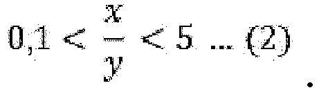
- a, b, x and y satisfy the following Equation (1) and Equation (2). 0.5 ⁇ a b ⁇ 1.5 0.1 ⁇ x y ⁇ 5
- the transmittance may be secured at 30% or higher when the Mo a Ti b O x N y layer is deposited to a thickness of 20 nm or greater, which is suited to be used as an electrochromic device.
- the x/y value is greater than 0.1 and less than 5
- the oxygen content is sufficient when the Mo a Ti b O x N y layer is deposited to a thickness of 20 nm or greater, and the transmittance may be secured at a certain level or higher.
- the ion storage layer may further include, in addition to the Mo a Ti b O x N y , LNO, NiO x1 (1.0 ⁇ x1 ⁇ 1.5), NiCrO x2 N y2 (3 ⁇ x2 ⁇ 6, 0.02 ⁇ y2 ⁇ 0.06) and the like.
- the ion storage layer has a thickness of greater than or equal to 20 nm and less than or equal to 100 nm.
- the ion storage layer has a refractive index of 1.8 to 2.9 at a 550 nm wavelength.
- the polymer electrolyte layer may be prepared using materials and methods known in the art. Specifically, a pentaerythritol triacrylate (PETA) monomer, 1 M or higher LiClO 4 , polycarbonate (PC) and the like may be used, however, the material and the method are not limited thereto.
- PETA pentaerythritol triacrylate
- PC polycarbonate
- the polymer electrolyte layer may include a lithium salt, a plasticizer, an oligomer, a monomer, an additive, a radical initiator and the like.
- the oligomer used in the present disclosure needs to have compatibility with the plasticizer.
- a preparation method including, for example, forming an electrolyte film by coating an electrolyte solution on a first release film, then laminating a second release film thereto and UV curing the result, transferring the electrolyte film on a first electrochromic unit after removing the first release film, and laminating a second electrochromic unit on the electrolyte film after removing the second release film may be used.
- first release film and the second release film materials known in the art may be used.
- the polymer electrolyte composition may have viscosity of 10 cps to 100,000 cps, and 1,000 cps to 5,000 cps based on 25°C.
- viscosity of the electrolyte solution satisfies the above-mentioned range, coating processability is excellent, and mixing process and defoaming process defects are prevented making film type coating simple.
- the polymer electrolyte layer has a thickness of each independently 10 ⁇ m to 500 ⁇ m.
- the electrochromic layer includes an oxide including tungsten (W).
- the electrochromic layer includes an oxide including tungsten (W), and may further include chromium (Cr), manganese (Mn), niobium (Nb) or the like.
- the electrochromic layer may include a thin film including an oxide including tungsten (W).
- the thin film may have density of 1 g/cm 3 to 4 g/cm 3 .
- the oxide including tungsten (W) may be represented by a chemical formula of WO z , and z is a real number of greater than or equal to 1 and less than or equal to 3.
- the oxide including tungsten (W) is tungsten trioxide (WO 3 ).
- the electrochromic layer has a thickness of greater than or equal to 10 nm and less than or equal to 1 ⁇ m.
- the electrochromic layer may be formed using methods known in the art.
- the electrochromic layer may also be formed using a method for manufacturing an electrochromic device to describe below.
- the electrochromic device described above may be further provided with a film on the second electrode.
- optical films generally known in the art may be used without limit as the film.
- triacetylcellulose, polyethylene terephthalate, polymethyl methacrylate, polycarbonate, acryl-based resins and the like may be used as the film material, and proper materials may be selected depending on the condition of the electrochromic device and unique properties of the optical film material.
- those having a thickness of greater than or equal to 50 ⁇ m and less than or equal to 200 ⁇ m may be used as the film.
- those having light transmittance of 70% or higher may be used as the film.
- Another embodiment of the present disclosure provides a method for manufacturing an electrochromic device including forming a first electrode on a substrate; forming an ion storage layer on the first electrode; forming an electrochromic layer on a second electrode; and forming a polymer electrolyte layer between the ion storage layer and the electrochromic layer, wherein the ion storage layer includes Mo a Ti b O x N y , and a, b, x and y are the same as or different from each other and each independently a real number of greater than or equal to 0.5 and less than or equal to 60.
- the forming of a first electrode on a substrate may use methods known in the art. For example, sputtering, electron beam deposition, chemical vapor deposition, a sol-gel coating method may be used on the substrate material described above for the formation, however, the method is not limited thereto.
- a first electrode may be formed on a substrate using direct current sputtering (DC sputtering).
- DC sputtering direct current sputtering
- lithium ion intercalation and deintercalation are difficult as thin film density increases, which becomes a factor inhibiting electrochromism efficiency. Accordingly, a process under a vacuum condition is suited so as to increase porosity of a thin film.
- the forming of an ion storage layer and the forming of an electrochromic layer may use the same method as the forming of a first electrode described above.
- the forming of an ion storage layer and the forming of an electrochromic layer may be conducted using a vacuum deposition method or direct current sputtering (DC sputtering).
- the forming of a polymer electrolyte layer may include forming a polymer electrolyte film by coating a polymer electrolyte solution on a first release film, then laminating a second release film thereto and UV curing the result, transferring the polymer electrolyte film on a first electrochromic unit after removing the first release film and, and laminating a second electrochromic unit on the polymer electrolyte film after removing the second release film.
- first release film and the second release film materials and methods known in the art may be used.
- the forming of a polymer electrolyte layer may include forming a polymer electrolyte film by coating a polymer electrolyte solution on the electrochromic layer and UV curing the result; and laminating the ion storage layer on the electrolyte film.
- the pentaerythritol triacrylate (PETA) monomer, the 1 M or higher LiClO 4 , the polycarbonate (PC) and the like described above may be used as the polymer electrolyte layer, and the polymer electrolyte layer may further include a lithium salt, a plasticizer, an oligomer, a monomer, an additive, a radical initiator and the like.
- WO 3 was deposited to a thickness of 300 nm as an electrochromic layer using a direct current sputtering method.
- LiNiO x was deposited to a thickness of 100 nm as an ion storage layer using a direct current sputtering method.
- the electrochromic layer and the ion storage layer were laminated using a gel polymer electrolyte to manufacture an electrochromic device.
- An electrochromic device was manufactured in the same manner as in Comparative Example 1 except that Mo a Ti b O x N y was deposited to a thickness of 50 nm as the ion storage layer.
- Each of the electrochromic devices of Comparative Example 1 and Example 1 went through electrochromic drive using a potentiostat apparatus, and optical properties were each measured using a UV-Vis spectrometer.
- Charge density of the electrode was measured using a potentiostat, and herein, a solution dissolving 1 mole of lithium perchlorate (LiClO 4 ) in a propylene carbonate (PC) solvent was used as the electrolyte, and PSCA was measured using the electrochromic material to evaluate as a working electrode, Pt as a counter electrode, and an Ag/AgCl wire as a reference electrode.
- the potential step chrono amperometry (PSCA) is repeating a constant voltage going in one direction at a constant speed and then changing the direction, and a current corresponding to a voltage applied to the electrode herein was measured.
- FIG. 2 is a graph showing charge density of the ion storage layer according to one embodiment of the present application. When referring to FIG. 2 , it was seen that charge density of the ion storage layer was most superior under the condition of ⁇ 5 V or higher.
- a current was measured by repeating a -5 V to +5 V section a few times at a rate of recording step 1 sec depending on a driving voltage section. Based on the graph obtained herein, coloring, bleaching peak currents and charge quantity were calculated. The area of the current-time profile was the charge quantity of the electrochromic material to evaluate, and the coloring, bleaching times were based on the 80% current amount with respect to the peak current.
- FIGs. 3 and 4 are graphs showing drive evaluation on the electrochromic device according to one embodiment of the present application.
- the electrochromic device according to one embodiment of the present application had excellent durability since a constant current value was maintained over time.
- the electrochromic device according to one embodiment of the present application had the electrochromic time decreasing by 10 times or greater compared to existing devices since low resistance properties of the electrochromic material were added when driving the device at a high voltage.
Landscapes
- Chemical & Material Sciences (AREA)
- Organic Chemistry (AREA)
- Inorganic Chemistry (AREA)
- Physics & Mathematics (AREA)
- Nonlinear Science (AREA)
- Optics & Photonics (AREA)
- General Physics & Mathematics (AREA)
- Environmental & Geological Engineering (AREA)
- Chemical Kinetics & Catalysis (AREA)
- Life Sciences & Earth Sciences (AREA)
- Electrochemistry (AREA)
- General Life Sciences & Earth Sciences (AREA)
- Geology (AREA)
- Engineering & Computer Science (AREA)
- Structural Engineering (AREA)
- Architecture (AREA)
- Civil Engineering (AREA)
- Electrochromic Elements, Electrophoresis, Or Variable Reflection Or Absorption Elements (AREA)
- Crystallography & Structural Chemistry (AREA)
Claims (11)
- Elektrochrome Vorrichtung, umfassend:ein Substrat (10);eine auf dem Substrat (10) vorgesehene erste Elektrode (11) ;eine auf der ersten Elektrode (11) vorgesehene Ionenspeicherschicht (12);eine auf der Ionenspeicherschicht (12) vorgesehene Polymer-Elektrolytschicht (3);eine auf der Polymer-Elektrolytschicht (3) vorgesehene elektrochrome Schicht (22); undeine auf der elektrochromen Schicht (22) vorgesehene zweite Elektrode (21),dadurch gekennzeichnet, dass die Ionenspeicherschicht (12) MoaTibOxNy umfasst; worin a, b, x und y gleich oder voneinander verschieden sind und jeweils unabhängig eine reale Zahl größer als oder gleich zu 0,5 und kleiner als oder gleich zu 60 darstellen.
- Elektrochrome Vorrichtung gemäß Anspruch 1, worin die Ionenspeicherschicht (12) eine Dicke größer als oder gleich zu 20 nm und kleiner als oder gleich zu 100 nm aufweist.
- Elektrochrome Vorrichtung gemäß Anspruch 1, worin die Ionenspeicherschicht (12) einen Brechungsindex von 1,8 bis 2,9 bei einer Wellenlänge von 550 nm aufweist.
- Elektrochrome Vorrichtung gemäß Anspruch 1, worin a, b, x und y die folgende Gleichung (1) und Gleichung (2) erfüllen:


- Elektrochrome Vorrichtung gemäß Anspruch 1, worin die elektrochrome Schicht (22) ein Oxid enthält, das Wolfram (W) enthält.
- Elektrochrome Vorrichtung gemäß Anspruch 1, worin die elektrochrome Schicht (22) eine Dicke von größer als oder gleich zu 20 nm und kleiner als oder gleich zu 1 µm aufweist.
- Elektrochrome Vorrichtung gemäß Anspruch 1, ferner umfassend einen optischen Film auf der zweiten Elektrode (21) .
- Verfahren zur Herstellung einer elektrochromen Vorrichtung, umfassend:Bilden einer ersten Elektrode (11) auf einem Substrat (10) ;Bilden einer Ionenspeicherschicht (12) auf der ersten Elektrode (11);Bilden einer elektrochromen Schicht (22) auf einer zweiten Elektrode (21); undBilden einer Polymer-Elektrolytschicht (3) zwischen der Ionenspeicherschicht (12) und der elektrochromen Schicht (22),dadurch gekennzeichnet, dass die Ionenspeicherschicht MoaTibOxNy umfasst; worin a, b, x und y gleich oder voneinander verschieden sind und jeweils unabhängig eine reale Zahl größer als oder gleich zu 0,5 und kleiner als oder gleich zu 60 darstellen.
- Verfahren zur Herstellung einer elektrochromen Vorrichtung gemäß Anspruch 8, worin das Bilden einer Ionenspeicherschicht und das Bilden einer elektrochromen Schicht durchgeführt werden unter Verwendung eines Vakuum-Abscheidungsverfahrens oder eines Gleichstrom-Sputterverfahrens (DC-Sputtern).
- Verfahren zur Herstellung einer elektrochromen Vorrichtung gemäß Anspruch 8, worin ab, b, x und y die folgende Gleichung (1) und Gleichung (2) erfüllen:

- Verfahren zur Herstellung einer elektrochromen Vorrichtung gemäß Anspruch 8, worin die elektrochrome Schicht (22) ein Oxid umfasst, das Wolfram (W) umfasst.
Applications Claiming Priority (2)
| Application Number | Priority Date | Filing Date | Title |
|---|---|---|---|
| KR1020160086251A KR102038739B1 (ko) | 2016-07-07 | 2016-07-07 | 전기변색 소자 및 그 제조방법 |
| PCT/KR2017/007239 WO2018009001A1 (ko) | 2016-07-07 | 2017-07-06 | 전기변색 소자 및 그 제조방법 |
Publications (3)
| Publication Number | Publication Date |
|---|---|
| EP3444663A1 EP3444663A1 (de) | 2019-02-20 |
| EP3444663A4 EP3444663A4 (de) | 2019-04-10 |
| EP3444663B1 true EP3444663B1 (de) | 2020-04-01 |
Family
ID=60913007
Family Applications (1)
| Application Number | Title | Priority Date | Filing Date |
|---|---|---|---|
| EP17824557.7A Active EP3444663B1 (de) | 2016-07-07 | 2017-07-06 | Elektrochrome vorrichtung und herstellungsverfahren dafür |
Country Status (5)
| Country | Link |
|---|---|
| US (1) | US10481457B2 (de) |
| EP (1) | EP3444663B1 (de) |
| KR (1) | KR102038739B1 (de) |
| CN (1) | CN109154756B (de) |
| WO (1) | WO2018009001A1 (de) |
Families Citing this family (1)
| Publication number | Priority date | Publication date | Assignee | Title |
|---|---|---|---|---|
| KR102202928B1 (ko) * | 2017-04-24 | 2021-01-14 | 주식회사 엘지화학 | 투광성 필름 및 이를 포함하는 전기변색소자 |
Family Cites Families (23)
| Publication number | Priority date | Publication date | Assignee | Title |
|---|---|---|---|---|
| KR20030072123A (ko) * | 2002-03-05 | 2003-09-13 | 주식회사 엘지이아이 | 전기변색소자 및 그 제조방법 |
| KR20060092362A (ko) * | 2005-02-17 | 2006-08-23 | 주식회사 엘지화학 | 전기변색소자 및 그 제조방법 |
| EP1739476A1 (de) * | 2005-07-01 | 2007-01-03 | Flabeg GmbH & Co. KG | Elektrochromes Element |
| DE102006044069A1 (de) | 2006-09-20 | 2008-03-27 | Bayer Materialscience Ag | Elektrochrome Anordnung |
| KR101085268B1 (ko) * | 2007-03-23 | 2011-11-22 | 주식회사 엘지화학 | 내수성이 우수한 전기변색소자용 전극 및 그 제조방법 |
| CN101833211B (zh) | 2010-04-01 | 2011-11-02 | 中国科学院宁波材料技术与工程研究所 | 一种智能调光玻璃 |
| KR101158425B1 (ko) | 2010-06-03 | 2012-07-03 | 곽준영 | 결정성 텅스텐 산화물 나노입자 분산형 졸겔(Sol-Gel) 코팅용액을 이용한 전기변색필름 및 그 제조방법 |
| KR101765915B1 (ko) * | 2010-12-23 | 2017-08-07 | 엘지이노텍 주식회사 | 전기 변색 소자를 적용한 디스플레이 장치 및 그 제어 방법 |
| CN102636931A (zh) * | 2011-02-15 | 2012-08-15 | 鸿富锦精密工业(深圳)有限公司 | 电致变色层、镀膜件及该镀膜件的制备方法 |
| US9535304B2 (en) | 2011-03-04 | 2017-01-03 | Thueringisches Institut Fuer Textil- Und Kunststoff-Forschung E.V. | Stable electrochromic module |
| DE102011013132A1 (de) * | 2011-03-04 | 2012-09-06 | Thüringisches Institut für Textil- und Kunststoff-Forschung e.V. | Stabiles elektrochromes Modul |
| CN102736342A (zh) * | 2011-04-01 | 2012-10-17 | 介面光电股份有限公司 | 电致变色装置 |
| JP5870182B2 (ja) | 2011-04-06 | 2016-02-24 | クロモジェニクス・アクチボラーグ | エレクトロクロミックデバイス |
| KR101816536B1 (ko) * | 2011-12-13 | 2018-01-10 | 동우 화인켐 주식회사 | 전기변색소자 및 그 제조방법 |
| KR101773817B1 (ko) | 2012-08-08 | 2017-09-04 | 한국전자통신연구원 | 거울 전환이 가능한 디스플레이 소자 |
| CN103771724B (zh) * | 2012-10-19 | 2016-12-21 | 中国南玻集团股份有限公司 | 全固态薄膜电致变色玻璃及其制备方法 |
| JP5946977B2 (ja) * | 2013-01-21 | 2016-07-06 | キネストラル テクノロジーズ,インク. | エレクトロクロミック性のリチウム・ニッケル・第5族混合金属酸化物 |
| KR102137519B1 (ko) * | 2014-01-15 | 2020-07-24 | 삼성전자주식회사 | 전기변색소자 |
| KR20150122319A (ko) * | 2014-04-22 | 2015-11-02 | 한국전자통신연구원 | 전기변색 소자의 제조방법 |
| KR20160011338A (ko) | 2014-07-22 | 2016-02-01 | 삼성전자주식회사 | 전기 변색소자 |
| CN105573002B (zh) * | 2014-10-09 | 2019-04-19 | 中国科学院宁波材料技术与工程研究所 | 一种具有信息存储功能的显示器件及其制备方法 |
| KR101638343B1 (ko) | 2014-12-26 | 2016-07-11 | 전자부품연구원 | 전기변색-열변색 하이브리드 소자 |
| CN104880884B (zh) | 2015-04-30 | 2018-10-12 | 游少鑫 | 一种电致变色智能玻璃及其制造方法 |
-
2016
- 2016-07-07 KR KR1020160086251A patent/KR102038739B1/ko active IP Right Grant
-
2017
- 2017-07-06 EP EP17824557.7A patent/EP3444663B1/de active Active
- 2017-07-06 WO PCT/KR2017/007239 patent/WO2018009001A1/ko active Application Filing
- 2017-07-06 CN CN201780029601.7A patent/CN109154756B/zh active Active
- 2017-07-06 US US16/307,833 patent/US10481457B2/en active Active
Also Published As
| Publication number | Publication date |
|---|---|
| US20190258127A1 (en) | 2019-08-22 |
| CN109154756A (zh) | 2019-01-04 |
| KR102038739B1 (ko) | 2019-10-30 |
| CN109154756B (zh) | 2021-04-27 |
| EP3444663A4 (de) | 2019-04-10 |
| WO2018009001A1 (ko) | 2018-01-11 |
| US10481457B2 (en) | 2019-11-19 |
| EP3444663A1 (de) | 2019-02-20 |
| KR20180005924A (ko) | 2018-01-17 |
Similar Documents
| Publication | Publication Date | Title |
|---|---|---|
| US5142406A (en) | Electrochromic optical switching device | |
| KR102010733B1 (ko) | 전기변색 소자 | |
| US20110299149A1 (en) | Transparent electrochromic plate and method for manufacture thereof | |
| KR102149672B1 (ko) | 전기변색 소자 | |
| KR20170109797A (ko) | 전기변색소자, 전기변색소자의 제조방법 및 그 투과율 제어방법 | |
| US20160011482A1 (en) | Electrochromic device comprising three or four layers | |
| KR102072882B1 (ko) | 전도성 구조체 및 이를 포함하는 전기변색 소자 | |
| EP3686666B1 (de) | Verfahren zur herstellung einer elektrochromen vorrichtung | |
| KR20170112183A (ko) | 전기변색소자 | |
| EP3444663B1 (de) | Elektrochrome vorrichtung und herstellungsverfahren dafür | |
| KR102079142B1 (ko) | 전기변색소자 | |
| JP2020518003A (ja) | 導電性積層体およびそれを含む電気変色素子 | |
| KR102108562B1 (ko) | 전기변색소자 | |
| KR102010754B1 (ko) | 전기변색소자 | |
| TWI450009B (zh) | 電致變色裝置及其製程方法 | |
| KR102010734B1 (ko) | 전기변색소자 | |
| KR102395150B1 (ko) | 전기변색필름 | |
| JP2003015164A (ja) | エレクトロクロミック素子 | |
| KR102395152B1 (ko) | 전기변색필름 | |
| RU2676807C2 (ru) | Электрохромное устройство и способ его изготовления | |
| KR20180122133A (ko) | 전기변색소자의 구동방법 | |
| JP2004101729A (ja) | 薄膜 | |
| JP2003043526A (ja) | エレクトロクロミック素子 | |
| KR20180122132A (ko) | 전기변색소자의 구동방법 | |
| KR102113478B1 (ko) | 전기변색필름, 전기변색소자 및 그 제조방법 |
Legal Events
| Date | Code | Title | Description |
|---|---|---|---|
| STAA | Information on the status of an ep patent application or granted ep patent |
Free format text: STATUS: THE INTERNATIONAL PUBLICATION HAS BEEN MADE |
|
| PUAI | Public reference made under article 153(3) epc to a published international application that has entered the european phase |
Free format text: ORIGINAL CODE: 0009012 |
|
| STAA | Information on the status of an ep patent application or granted ep patent |
Free format text: STATUS: REQUEST FOR EXAMINATION WAS MADE |
|
| 17P | Request for examination filed |
Effective date: 20181113 |
|
| AK | Designated contracting states |
Kind code of ref document: A1 Designated state(s): AL AT BE BG CH CY CZ DE DK EE ES FI FR GB GR HR HU IE IS IT LI LT LU LV MC MK MT NL NO PL PT RO RS SE SI SK SM TR |
|
| AX | Request for extension of the european patent |
Extension state: BA ME |
|
| A4 | Supplementary search report drawn up and despatched |
Effective date: 20190311 |
|
| RIC1 | Information provided on ipc code assigned before grant |
Ipc: C01G 41/02 20060101ALN20190305BHEP Ipc: G02F 1/153 20060101ALI20190305BHEP Ipc: E06B 9/24 20060101ALN20190305BHEP Ipc: E06B 3/67 20060101ALN20190305BHEP Ipc: C01G 39/00 20060101ALN20190305BHEP Ipc: C01G 23/00 20060101ALN20190305BHEP Ipc: G02F 1/1523 20190101AFI20190305BHEP Ipc: G02F 1/15 20190101ALI20190305BHEP |
|
| DAV | Request for validation of the european patent (deleted) | ||
| DAX | Request for extension of the european patent (deleted) | ||
| REG | Reference to a national code |
Ref country code: DE Ref legal event code: R079 Ref document number: 602017014148 Country of ref document: DE Free format text: PREVIOUS MAIN CLASS: G02F0001150000 Ipc: G02F0001152300 |
|
| GRAP | Despatch of communication of intention to grant a patent |
Free format text: ORIGINAL CODE: EPIDOSNIGR1 |
|
| RIC1 | Information provided on ipc code assigned before grant |
Ipc: E06B 3/67 20060101ALN20191125BHEP Ipc: C01G 39/00 20060101ALN20191125BHEP Ipc: E06B 9/24 20060101ALN20191125BHEP Ipc: G02F 1/1523 20190101AFI20191125BHEP Ipc: G02F 1/153 20060101ALI20191125BHEP Ipc: C01G 41/02 20060101ALN20191125BHEP Ipc: C01G 23/00 20060101ALN20191125BHEP Ipc: G02F 1/15 20190101ALI20191125BHEP |
|
| STAA | Information on the status of an ep patent application or granted ep patent |
Free format text: STATUS: GRANT OF PATENT IS INTENDED |
|
| INTG | Intention to grant announced |
Effective date: 20200102 |
|
| GRAS | Grant fee paid |
Free format text: ORIGINAL CODE: EPIDOSNIGR3 |
|
| GRAA | (expected) grant |
Free format text: ORIGINAL CODE: 0009210 |
|
| STAA | Information on the status of an ep patent application or granted ep patent |
Free format text: STATUS: THE PATENT HAS BEEN GRANTED |
|
| REG | Reference to a national code |
Ref country code: DE Ref legal event code: R082 Ref document number: 602017014148 Country of ref document: DE Representative=s name: HOFFMANN - EITLE PATENT- UND RECHTSANWAELTE PA, DE |
|
| AK | Designated contracting states |
Kind code of ref document: B1 Designated state(s): AL AT BE BG CH CY CZ DE DK EE ES FI FR GB GR HR HU IE IS IT LI LT LU LV MC MK MT NL NO PL PT RO RS SE SI SK SM TR |
|
| REG | Reference to a national code |
Ref country code: GB Ref legal event code: FG4D |
|
| REG | Reference to a national code |
Ref country code: CH Ref legal event code: EP Ref country code: AT Ref legal event code: REF Ref document number: 1252138 Country of ref document: AT Kind code of ref document: T Effective date: 20200415 |
|
| REG | Reference to a national code |
Ref country code: DE Ref legal event code: R096 Ref document number: 602017014148 Country of ref document: DE |
|
| REG | Reference to a national code |
Ref country code: IE Ref legal event code: FG4D |
|
| PG25 | Lapsed in a contracting state [announced via postgrant information from national office to epo] |
Ref country code: BG Free format text: LAPSE BECAUSE OF FAILURE TO SUBMIT A TRANSLATION OF THE DESCRIPTION OR TO PAY THE FEE WITHIN THE PRESCRIBED TIME-LIMIT Effective date: 20200701 |
|
| REG | Reference to a national code |
Ref country code: NL Ref legal event code: MP Effective date: 20200401 |
|
| REG | Reference to a national code |
Ref country code: LT Ref legal event code: MG4D |
|
| PG25 | Lapsed in a contracting state [announced via postgrant information from national office to epo] |
Ref country code: LT Free format text: LAPSE BECAUSE OF FAILURE TO SUBMIT A TRANSLATION OF THE DESCRIPTION OR TO PAY THE FEE WITHIN THE PRESCRIBED TIME-LIMIT Effective date: 20200401 Ref country code: CZ Free format text: LAPSE BECAUSE OF FAILURE TO SUBMIT A TRANSLATION OF THE DESCRIPTION OR TO PAY THE FEE WITHIN THE PRESCRIBED TIME-LIMIT Effective date: 20200401 Ref country code: PT Free format text: LAPSE BECAUSE OF FAILURE TO SUBMIT A TRANSLATION OF THE DESCRIPTION OR TO PAY THE FEE WITHIN THE PRESCRIBED TIME-LIMIT Effective date: 20200817 Ref country code: NL Free format text: LAPSE BECAUSE OF FAILURE TO SUBMIT A TRANSLATION OF THE DESCRIPTION OR TO PAY THE FEE WITHIN THE PRESCRIBED TIME-LIMIT Effective date: 20200401 Ref country code: FI Free format text: LAPSE BECAUSE OF FAILURE TO SUBMIT A TRANSLATION OF THE DESCRIPTION OR TO PAY THE FEE WITHIN THE PRESCRIBED TIME-LIMIT Effective date: 20200401 Ref country code: SE Free format text: LAPSE BECAUSE OF FAILURE TO SUBMIT A TRANSLATION OF THE DESCRIPTION OR TO PAY THE FEE WITHIN THE PRESCRIBED TIME-LIMIT Effective date: 20200401 Ref country code: IS Free format text: LAPSE BECAUSE OF FAILURE TO SUBMIT A TRANSLATION OF THE DESCRIPTION OR TO PAY THE FEE WITHIN THE PRESCRIBED TIME-LIMIT Effective date: 20200801 Ref country code: NO Free format text: LAPSE BECAUSE OF FAILURE TO SUBMIT A TRANSLATION OF THE DESCRIPTION OR TO PAY THE FEE WITHIN THE PRESCRIBED TIME-LIMIT Effective date: 20200701 Ref country code: GR Free format text: LAPSE BECAUSE OF FAILURE TO SUBMIT A TRANSLATION OF THE DESCRIPTION OR TO PAY THE FEE WITHIN THE PRESCRIBED TIME-LIMIT Effective date: 20200702 |
|
| REG | Reference to a national code |
Ref country code: AT Ref legal event code: MK05 Ref document number: 1252138 Country of ref document: AT Kind code of ref document: T Effective date: 20200401 |
|
| PG25 | Lapsed in a contracting state [announced via postgrant information from national office to epo] |
Ref country code: RS Free format text: LAPSE BECAUSE OF FAILURE TO SUBMIT A TRANSLATION OF THE DESCRIPTION OR TO PAY THE FEE WITHIN THE PRESCRIBED TIME-LIMIT Effective date: 20200401 Ref country code: HR Free format text: LAPSE BECAUSE OF FAILURE TO SUBMIT A TRANSLATION OF THE DESCRIPTION OR TO PAY THE FEE WITHIN THE PRESCRIBED TIME-LIMIT Effective date: 20200401 Ref country code: LV Free format text: LAPSE BECAUSE OF FAILURE TO SUBMIT A TRANSLATION OF THE DESCRIPTION OR TO PAY THE FEE WITHIN THE PRESCRIBED TIME-LIMIT Effective date: 20200401 |
|
| PG25 | Lapsed in a contracting state [announced via postgrant information from national office to epo] |
Ref country code: AL Free format text: LAPSE BECAUSE OF FAILURE TO SUBMIT A TRANSLATION OF THE DESCRIPTION OR TO PAY THE FEE WITHIN THE PRESCRIBED TIME-LIMIT Effective date: 20200401 |
|
| REG | Reference to a national code |
Ref country code: DE Ref legal event code: R097 Ref document number: 602017014148 Country of ref document: DE |
|
| PG25 | Lapsed in a contracting state [announced via postgrant information from national office to epo] |
Ref country code: IT Free format text: LAPSE BECAUSE OF FAILURE TO SUBMIT A TRANSLATION OF THE DESCRIPTION OR TO PAY THE FEE WITHIN THE PRESCRIBED TIME-LIMIT Effective date: 20200401 Ref country code: SM Free format text: LAPSE BECAUSE OF FAILURE TO SUBMIT A TRANSLATION OF THE DESCRIPTION OR TO PAY THE FEE WITHIN THE PRESCRIBED TIME-LIMIT Effective date: 20200401 Ref country code: EE Free format text: LAPSE BECAUSE OF FAILURE TO SUBMIT A TRANSLATION OF THE DESCRIPTION OR TO PAY THE FEE WITHIN THE PRESCRIBED TIME-LIMIT Effective date: 20200401 Ref country code: RO Free format text: LAPSE BECAUSE OF FAILURE TO SUBMIT A TRANSLATION OF THE DESCRIPTION OR TO PAY THE FEE WITHIN THE PRESCRIBED TIME-LIMIT Effective date: 20200401 Ref country code: ES Free format text: LAPSE BECAUSE OF FAILURE TO SUBMIT A TRANSLATION OF THE DESCRIPTION OR TO PAY THE FEE WITHIN THE PRESCRIBED TIME-LIMIT Effective date: 20200401 Ref country code: AT Free format text: LAPSE BECAUSE OF FAILURE TO SUBMIT A TRANSLATION OF THE DESCRIPTION OR TO PAY THE FEE WITHIN THE PRESCRIBED TIME-LIMIT Effective date: 20200401 Ref country code: DK Free format text: LAPSE BECAUSE OF FAILURE TO SUBMIT A TRANSLATION OF THE DESCRIPTION OR TO PAY THE FEE WITHIN THE PRESCRIBED TIME-LIMIT Effective date: 20200401 |
|
| PLBE | No opposition filed within time limit |
Free format text: ORIGINAL CODE: 0009261 |
|
| STAA | Information on the status of an ep patent application or granted ep patent |
Free format text: STATUS: NO OPPOSITION FILED WITHIN TIME LIMIT |
|
| PG25 | Lapsed in a contracting state [announced via postgrant information from national office to epo] |
Ref country code: PL Free format text: LAPSE BECAUSE OF FAILURE TO SUBMIT A TRANSLATION OF THE DESCRIPTION OR TO PAY THE FEE WITHIN THE PRESCRIBED TIME-LIMIT Effective date: 20200401 Ref country code: SK Free format text: LAPSE BECAUSE OF FAILURE TO SUBMIT A TRANSLATION OF THE DESCRIPTION OR TO PAY THE FEE WITHIN THE PRESCRIBED TIME-LIMIT Effective date: 20200401 Ref country code: MC Free format text: LAPSE BECAUSE OF FAILURE TO SUBMIT A TRANSLATION OF THE DESCRIPTION OR TO PAY THE FEE WITHIN THE PRESCRIBED TIME-LIMIT Effective date: 20200401 |
|
| REG | Reference to a national code |
Ref country code: CH Ref legal event code: PL |
|
| 26N | No opposition filed |
Effective date: 20210112 |
|
| REG | Reference to a national code |
Ref country code: BE Ref legal event code: MM Effective date: 20200731 |
|
| PG25 | Lapsed in a contracting state [announced via postgrant information from national office to epo] |
Ref country code: CH Free format text: LAPSE BECAUSE OF NON-PAYMENT OF DUE FEES Effective date: 20200731 Ref country code: IE Free format text: LAPSE BECAUSE OF NON-PAYMENT OF DUE FEES Effective date: 20200706 Ref country code: LU Free format text: LAPSE BECAUSE OF NON-PAYMENT OF DUE FEES Effective date: 20200706 Ref country code: LI Free format text: LAPSE BECAUSE OF NON-PAYMENT OF DUE FEES Effective date: 20200731 |
|
| PG25 | Lapsed in a contracting state [announced via postgrant information from national office to epo] |
Ref country code: SI Free format text: LAPSE BECAUSE OF FAILURE TO SUBMIT A TRANSLATION OF THE DESCRIPTION OR TO PAY THE FEE WITHIN THE PRESCRIBED TIME-LIMIT Effective date: 20200401 Ref country code: BE Free format text: LAPSE BECAUSE OF NON-PAYMENT OF DUE FEES Effective date: 20200731 |
|
| PG25 | Lapsed in a contracting state [announced via postgrant information from national office to epo] |
Ref country code: TR Free format text: LAPSE BECAUSE OF FAILURE TO SUBMIT A TRANSLATION OF THE DESCRIPTION OR TO PAY THE FEE WITHIN THE PRESCRIBED TIME-LIMIT Effective date: 20200401 Ref country code: MT Free format text: LAPSE BECAUSE OF FAILURE TO SUBMIT A TRANSLATION OF THE DESCRIPTION OR TO PAY THE FEE WITHIN THE PRESCRIBED TIME-LIMIT Effective date: 20200401 Ref country code: CY Free format text: LAPSE BECAUSE OF FAILURE TO SUBMIT A TRANSLATION OF THE DESCRIPTION OR TO PAY THE FEE WITHIN THE PRESCRIBED TIME-LIMIT Effective date: 20200401 |
|
| PG25 | Lapsed in a contracting state [announced via postgrant information from national office to epo] |
Ref country code: MK Free format text: LAPSE BECAUSE OF FAILURE TO SUBMIT A TRANSLATION OF THE DESCRIPTION OR TO PAY THE FEE WITHIN THE PRESCRIBED TIME-LIMIT Effective date: 20200401 |
|
| PGFP | Annual fee paid to national office [announced via postgrant information from national office to epo] |
Ref country code: FR Payment date: 20230621 Year of fee payment: 7 |
|
| PGFP | Annual fee paid to national office [announced via postgrant information from national office to epo] |
Ref country code: GB Payment date: 20230620 Year of fee payment: 7 |
|
| PGFP | Annual fee paid to national office [announced via postgrant information from national office to epo] |
Ref country code: DE Payment date: 20230620 Year of fee payment: 7 |