EP3410084A1 - Infrarotsensor - Google Patents
Infrarotsensor Download PDFInfo
- Publication number
- EP3410084A1 EP3410084A1 EP17744396.7A EP17744396A EP3410084A1 EP 3410084 A1 EP3410084 A1 EP 3410084A1 EP 17744396 A EP17744396 A EP 17744396A EP 3410084 A1 EP3410084 A1 EP 3410084A1
- Authority
- EP
- European Patent Office
- Prior art keywords
- insulating film
- pair
- adhesive
- film
- pattern wiring
- Prior art date
- Legal status (The legal status is an assumption and is not a legal conclusion. Google has not performed a legal analysis and makes no representation as to the accuracy of the status listed.)
- Granted
Links
Images


Classifications
-
- G—PHYSICS
- G01—MEASURING; TESTING
- G01J—MEASUREMENT OF INTENSITY, VELOCITY, SPECTRAL CONTENT, POLARISATION, PHASE OR PULSE CHARACTERISTICS OF INFRARED, VISIBLE OR ULTRAVIOLET LIGHT; COLORIMETRY; RADIATION PYROMETRY
- G01J5/00—Radiation pyrometry, e.g. infrared or optical thermometry
- G01J5/10—Radiation pyrometry, e.g. infrared or optical thermometry using electric radiation detectors
- G01J5/20—Radiation pyrometry, e.g. infrared or optical thermometry using electric radiation detectors using resistors, thermistors or semiconductors sensitive to radiation, e.g. photoconductive devices
-
- G—PHYSICS
- G01—MEASURING; TESTING
- G01J—MEASUREMENT OF INTENSITY, VELOCITY, SPECTRAL CONTENT, POLARISATION, PHASE OR PULSE CHARACTERISTICS OF INFRARED, VISIBLE OR ULTRAVIOLET LIGHT; COLORIMETRY; RADIATION PYROMETRY
- G01J5/00—Radiation pyrometry, e.g. infrared or optical thermometry
- G01J5/10—Radiation pyrometry, e.g. infrared or optical thermometry using electric radiation detectors
-
- G—PHYSICS
- G01—MEASURING; TESTING
- G01J—MEASUREMENT OF INTENSITY, VELOCITY, SPECTRAL CONTENT, POLARISATION, PHASE OR PULSE CHARACTERISTICS OF INFRARED, VISIBLE OR ULTRAVIOLET LIGHT; COLORIMETRY; RADIATION PYROMETRY
- G01J1/00—Photometry, e.g. photographic exposure meter
- G01J1/02—Details
-
- G—PHYSICS
- G01—MEASURING; TESTING
- G01J—MEASUREMENT OF INTENSITY, VELOCITY, SPECTRAL CONTENT, POLARISATION, PHASE OR PULSE CHARACTERISTICS OF INFRARED, VISIBLE OR ULTRAVIOLET LIGHT; COLORIMETRY; RADIATION PYROMETRY
- G01J5/00—Radiation pyrometry, e.g. infrared or optical thermometry
- G01J5/02—Constructional details
-
- G—PHYSICS
- G01—MEASURING; TESTING
- G01J—MEASUREMENT OF INTENSITY, VELOCITY, SPECTRAL CONTENT, POLARISATION, PHASE OR PULSE CHARACTERISTICS OF INFRARED, VISIBLE OR ULTRAVIOLET LIGHT; COLORIMETRY; RADIATION PYROMETRY
- G01J5/00—Radiation pyrometry, e.g. infrared or optical thermometry
- G01J5/10—Radiation pyrometry, e.g. infrared or optical thermometry using electric radiation detectors
- G01J2005/103—Absorbing heated plate or film and temperature detector
Definitions
- the present invention relates to an infrared sensor having an excellent responsivity that is suitable for measuring a temperature of a heat roller used in a copying machine, printer, or the like.
- an infrared sensor installed opposing to the object to be measured so as to measure the temperature by receiving radiant heat from the object.
- a film-type infrared sensor has been developed as one of such infrared sensors, in which a thin film thermistor is formed on an insulating film so that the sensor can have an excellent flexibility and a thin profile as a whole.
- Patent document 1 discloses an infrared sensor that includes an insulating film; first and second heat sensitive elements that are provided so as to be spaced apart from each other on either surface of the insulating film; first and second conductive wiring films that are formed on either surface of the insulating film and connected to first and second heat sensitive elements respectively; and an infrared reflection film that is provided on the other surface of the insulating film so as to oppose to the second heat sensitive element.
- the heat collection from a part of the insulating film that absorbs infrared radiation has been improved by increasing the area of the wiring film formed on the side for receiving infrared radiation.
- Patent Document 1 Japanese Unexamined Patent Application Publication No. 2013-160635
- the present invention has been made in view of the aforementioned circumstances, and an object of the present invention is to provide an infrared sensor that allows heat to be efficiently transferred from an insulating film to a heat sensitive element and has a good responsivity.
- an infrared sensor comprises: an insulating film; a pair of adhesive electrodes that is patterned on either surface of the insulating film; a pair of terminal electrodes that is patterned on either surface of the insulating film; a heat sensitive element that is provided on either surface of the insulating film and is connected to the pair of adhesive electrodes; a pair of pattern wiring parts that is patterned on either surface of the insulating film with one end thereof being connected to the pair of adhesive electrodes and the other end thereof being connected to the pair of terminal electrodes; and a heat transfer film that is connected to the adhesive electrode besides the pattern wiring part and is patterned in the vicinity of the adhesive electrode on either surface of the insulating film using a thin film having a higher thermal conductivity than that of the insulating film.
- the infrared sensor according to the first aspect of the present invention comprises the heat transfer film that is connected to the adhesive electrode besides the pattern wiring part and is patterned in the vicinity of the adhesive electrode on either surface of the insulating film using a thin film having a higher thermal conductivity than that of the insulating film, the heat absorbed in the insulating film can be difficult to be transferred to the side of the terminal electrode while it can be preferentially transferred to the heat sensitive element through the heat transfer film. Specifically, by controlling the direction of the flow of heat resulting from the infrared radiation that is received by the insulating film to the adhesive electrode through the heat transfer film, most of the received infrared energy can be efficiently utilized for increasing or decreasing the temperature of the heat sensitive element.
- An infrared sensor according to a second aspect of the present invention is characterized by the infrared sensor according to the first aspect of the present invention, wherein the heat transfer film is formed so as to have a larger area than that of the pattern wiring part.
- the heat transfer film since the heat transfer film is formed so as to have a larger area than that of the pattern wiring part, the heat transfer film can receive more heat from the insulating film than the pattern wiring part, which allows more heat to be transferred to the heat sensitive element.
- An infrared sensor according to a third aspect of the present invention is characterized by the infrared sensor according to the first or second aspect, wherein the pattern wiring part extends from the adhesive electrode towards the side opposite to the terminal electrode and further extends along a part of the outer periphery of the heat transfer film so as to reach the terminal electrode.
- the pattern wiring part extends from the adhesive electrode towards the side opposite to the terminal electrode and further extends along a part of the outer periphery of the heat transfer film so as to reach the terminal electrode, the pattern wiring part extends for a long distance so as to increase the thermal resistance and also extends once towards the side opposite to the terminal electrode so as to allow further suppression of the heat flow to the terminal electrode.
- An infrared sensor according to a fourth aspect of the present invention is characterized by the infrared sensor according to any one of the first to third aspects, wherein the connection width of the heat transfer film to the adhesive electrode is set to be wilder than that of the pattern wiring part to the adhesive electrode.
- connection width of the heat transfer film to the adhesive electrode is set to be wilder than that of the pattern wiring part to the adhesive electrode, heat can be efficiently transferred from the heat transfer film to the adhesive electrode while it can be difficult to be transferred from the adhesive electrode to the pattern wiring part.
- An infrared sensor according to a fifth aspect of the present invention is characterized by the infrared sensor according to any one of the first to fourth aspects, wherein the pattern wiring part has a tortuous portion formed by several folding.
- the thermal resistance to the terminal electrode can be increased.
- the infrared sensor of the present invention comprises the heat transfer film that is connected to the adhesive electrode besides the pattern wiring part and is patterned in the vicinity of the adhesive electrode on either surface of the insulating film using a thin film having a higher thermal conductivity than that of the insulating film, the heat absorbed in the insulating film can be difficult to be transferred to the side of the terminal electrode while it can be preferentially transferred to the heat sensitive element through the heat transfer film.
- the present sensor since the heat resulting from the received infrared radiation is positively guided to the heat sensitive element through the heat transfer film so as to reduce the thermal resistance, more heat can be transferred to the heat sensitive element. Therefore the present sensor has a high responsivity and is suitable for measuring a temperature of a heat roller used in a copying machine, printer, or the like.
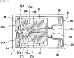
- an infrared sensor 1 includes an insulating film 2, a pair of first adhesive electrodes 3A that is patterned on either surface(face) of the insulating film 2, a pair of first terminal electrodes 4A that is patterned on either surface of the insulating film 2, a first heat sensitive element 5A that is provided on either surface of the insulating film 2 and is connected to the pair of first adhesive electrodes 3A, a pair of first pattern wiring parts 6A that is patterned on either surface of the insulating film 2 with one end thereof being connected to the pair of first adhesive electrodes 3A and the other end thereof being connected to the pair of first terminal electrodes 4A; and a pair of heat transfer films 7 that is connected to the pair of first adhesive electrodes 3A besides the first pattern wiring parts 6A and is patterned in the vicinity of the adhesive electrodes 3A on either surface of the insulating film 2 using a thin film having a higher thermal conductivity than that of the insulating film 2.
- the first pattern wiring part 6A and the heat transfer film 7 are not in a direct contact with each other, but are indirectly connected to each other through the first adhesive electrode 3A.
- the infrared sensor 1 also includes a pair of second adhesive electrodes 3B that is patterned on either surface of the insulating film 2; a pair of second terminal electrodes 4B that is patterned on either surface of the insulating film 2; a second heat sensitive element 5B that is provided on either surface of the insulating film 2, is connected to the pair of second adhesive electrodes 3B, and is arranged spaced apart from the first heat sensitive element 5A; and a pair of second pattern wiring parts 6B that is patterned on either surface of the insulating film 2 with one end thereof being connected to the pair of second adhesive electrodes 3B and the other end thereof being connected to the pair of second terminal electrodes 4B.
- the heat transfer film 7 is formed so as to have a larger area than that of the first pattern wiring part 6A.
- the pair of first pattern wiring parts 6A extends from the pair of first adhesive electrodes 3A towards the side opposite to the pair of first terminal electrodes 4A and further extends along a part of the outer periphery of the pair of heat transfer films 7 so as to reach their respective first terminal electrodes 4A.
- the first pattern wiring parts 6A first extend from the first adhesive electrodes 3A between the pair of heat transfer films 7 towards the second heat sensitive element 5B, and then extend in the direction along the short side of the insulating film 2 towards the long side thereof in the vicinity of the end of the pair of heat transfer films 7, and further extend outside the heat transfer films 7 along the long side of the insulating film 2 to the first terminal electrodes 4A.
- the second pattern wiring part 6B extends for a shorter distance than the first pattern wiring part 6A so as to reach the second terminal electrode 4B.
- connection width of the heat transfer film 7 to the first adhesive electrode 3A is set to be wilder than that of the first pattern wiring part 6A to the first adhesive electrode 3A.
- the heat transfer film 7 is connected to entirely two of the four sides of the first adhesive electrode 3A having a square shape, whereas the first pattern wiring part 6A is connected to one of the four corners of the first adhesive electrode 3A.
- the connecting part of the heat transfer film 7 to the first adhesive electrode 3A is set separately from the connecting part of the first pattern wiring part 6A to the first adhesive electrode 3A.
- first adhesive electrode 3A and a second adhesive electrode 3B are adhered their respective terminal electrodes of the first heat sensitive element 5A and the second heat sensitive element 5B with a conductive adhesive such as a solder.
- an infrared reflection film 8 is formed so as to cover the portion immediately above the second heat sensitive element 5B. This infrared reflection film 8 is formed so as to avoid the portion immediately above the pair of heat transfer films 7.
- the first heat sensitive element 5A that is arranged immediately under the surface for receiving infrared radiation is an element for detecting infrared radiation
- the second heat sensitive element 5B that is arranged immediately under the infrared reflection film 8 is an element for compensation.
- each of the terminal electrodes, each of the pattern wiring parts, the heat transfer films 7, and the infrared reflection film 8 are indicated by hatching in FIG. 1(a) and (b) .
- the insulating film 2 is made of a polyimide resin sheet having a generally rectangular shape, while the infrared reflection film 8, each of the pattern wiring parts, each of the terminal electrodes, each of the adhesive electrodes, and the heat transfer films 7 are made of a copper foil. Specifically, these elements compose a double-sided flexible substrate in which the infrared reflection film 8, each of the pattern wiring parts, each of the terminal electrodes, each of the adhesive electrodes, and the heat transfer films 7 made of copper foil are patterned on both surfaces of the insulating film 2 as a polyimide substrate.
- the pair of first terminal electrodes 4A and the pair of second terminal electrodes 4B are arranged in the vicinity of the corners of the insulating film 2.
- the infrared reflection film 8 is composed of the copper foil as described above and a gold plating film that is laminated on the copper foil.
- This infrared reflection film 8 is made of a material having a higher infrared reflectance than that of the insulating film 2 and is formed by coating a copper foil with a gold plating film as described above.
- This film may be made of, for example, a mirror finished aluminum vapor-deposited film, aluminum foil, or the like other than the gold plating film.
- the first heat sensitive element 5A and the second heat sensitive element 5B are chip thermistors at both ends of which terminal electrodes (not shown) are formed.
- Such thermistors include NTC-type, PTC-type, CTR-type thermistors, and the like, but in the present embodiment, a NTC-type thermistor is employed for the first heat sensitive element 5A and the second heat sensitive element 5B, for example.
- This thermistor is made of a Mn-Co-Cu or Mn-Co-Fe based thermistor material, or the like.
- the infrared sensor 1 of the present embodiment includes the heat transfer film 7 that are connected to the first adhesive electrode 3A besides the first pattern wiring part 6A and are patterned on either surface of the insulating film 2 in the vicinity of the first adhesive electrode 3A using a thin film having a higher thermal conductivity than that of the insulating film 2, the heat absorbed in the insulating film 2 can be difficult to be transferred to the side of the first terminal electrode 4A while it can be preferentially transferred to the first heat sensitive element 5A through the heat transfer film 7.
- the heat transfer film 7 is formed so as to have a larger area than that of the first pattern wiring part 6A, the heat transfer film 7 can receive more heat from the insulating film 2 than the first pattern wiring part 6A, which allows more heat to be transferred to the first heat sensitive element 5A.
- the first pattern wiring part 6A extends from the first adhesive electrode 3A towards the side opposite to the first terminal electrode 4A and further extends along a part of the outer periphery of the heat transfer film 7 so as to reach the first terminal electrode 4A, the first pattern wiring part 6A extends for a long distance so as to increase the thermal resistance and also extends once towards the side opposite to the first terminal electrode 4A so as to allow further suppression of the heat flow to the first terminal electrode 4A.
- connection width of the heat transfer film 7 to the first adhesive electrode 3A is set to be wilder than that of the first pattern wiring part 6A to the first adhesive electrode 3A, heat can be efficiently transferred from the heat transfer film 7 to the first adhesive electrode 3A while it can be difficult to be transferred from the first adhesive electrode 3A to the first pattern wiring part 6A.
- infrared sensors according to a second and third embodiments of the present invention will be described below with reference to FIGs. 2 and 3 .
- the same components as those in the first embodiment described above are denoted by the same reference numerals, and thus the description thereof is omitted.
- the infrared reflection film 8 formed on the other surface of the insulating film 2 is indicated with a dashed line.
- the second embodiment is different from the first embodiment in the following points.
- the heat transfer film 7 is connected without any gap to entirely two of the four sides of the first adhesive electrode 3A having a square shape
- the heat transfer film 27 is connected to partially two of the four sides of the first adhesive electrode 3A having a square shape through a constricted portion 27a.
- a concave portion 27b is formed at the connecting part of the heat transfer film 27 to the two sides adjacent to each other of the first adhesive electrode 3A so as to define the constricted portion 27a that is a narrower portion of the connecting part.
- constricted portion 27a is formed at the connecting part of the heat transfer film 27 to the first adhesive electrode 3A and the constricted portion 27a can function as a thermal land, heat does not escape to the surrounding area beyond necessity during soldering, and as a result, poor soldering resulting from undissolved solder can be suppressed. Even in this case, since the first pattern wiring part 6A that is thin is connected to only one side of the first adhesive electrode 3A, heat from the first adhesive electrode 3A can be difficult to be transferred to the first pattern wiring part 6A.
- the end of the heat transfer film 27 on the side of the first terminal electrode 4A is formed so as to have a larger size than in the first embodiment. Specifically, since the end of the heat transfer film 27 is formed so as to extend to the portion between the pair of first terminal electrodes 4A, the heat collection of the heat transfer film 27 can be improved.
- the first pattern wiring parts 6A extend from the first adhesive electrodes 3A towards the side of the second heat sensitive element 5B and further extend outside the heat transfer films 27 so as to reach the first terminal electrodes 4A
- a pair of first pattern wiring parts 36A extends from the pair of first adhesive electrodes 3A to the direction opposite to that in the first embodiment and then passes through tortuous portions 36a formed by several folding so as to reach their respective first terminal electrodes 4A.
- the first pattern wiring part 36A since the first pattern wiring part 36A has the tortuous portion 36a, the thermal resistance to the first terminal electrode 4A can be increased. Therefore, the first pattern wiring part 6A can extend for a long distance without extending once towards the side of the second heat sensitive element 5B and taking a bypass route outside the heat transfer film 37 as in the second embodiment, which can suppress the heat transfer to the first terminal electrode 4A.
- the first heat sensitive element is configured to detect the heat transferred from the insulating film that directly receives infrared radiation
- an infrared absorbing film having a higher infrared absorbency than that of the insulating film may be formed immediately above the first heat sensitive element and on either surface of the insulating film.
- the infrared absorbing effect can be further improved in the first heat sensitive element, and thus a favorable temperature difference between the first heat sensitive element and the second heat sensitive element can be obtained.
- this infrared absorbing film may be configured to absorb infrared radiation radiated from an object to be measured, and then the heat from the infrared absorbing film, which absorbs infrared radiation and generates heat, is transferred through the insulating film so as to allow the temperature of the first heat sensitive element immediately below the film to be changed.
Landscapes
- Physics & Mathematics (AREA)
- General Physics & Mathematics (AREA)
- Spectroscopy & Molecular Physics (AREA)
- Photometry And Measurement Of Optical Pulse Characteristics (AREA)
- Radiation Pyrometers (AREA)
Applications Claiming Priority (2)
| Application Number | Priority Date | Filing Date | Title |
|---|---|---|---|
| JP2016016512A JP6677925B2 (ja) | 2016-01-29 | 2016-01-29 | 赤外線センサ |
| PCT/JP2017/002960 WO2017131166A1 (ja) | 2016-01-29 | 2017-01-27 | 赤外線センサ |
Publications (3)
| Publication Number | Publication Date |
|---|---|
| EP3410084A1 true EP3410084A1 (de) | 2018-12-05 |
| EP3410084A4 EP3410084A4 (de) | 2019-09-04 |
| EP3410084B1 EP3410084B1 (de) | 2024-03-13 |
Family
ID=59398264
Family Applications (1)
| Application Number | Title | Priority Date | Filing Date |
|---|---|---|---|
| EP17744396.7A Active EP3410084B1 (de) | 2016-01-29 | 2017-01-27 | Infrarotsensor |
Country Status (6)
| Country | Link |
|---|---|
| US (1) | US11118980B2 (de) |
| EP (1) | EP3410084B1 (de) |
| JP (1) | JP6677925B2 (de) |
| KR (1) | KR20180105132A (de) |
| CN (1) | CN108351249A (de) |
| WO (1) | WO2017131166A1 (de) |
Families Citing this family (1)
| Publication number | Priority date | Publication date | Assignee | Title |
|---|---|---|---|---|
| JP6743737B2 (ja) * | 2017-03-24 | 2020-08-19 | 三菱マテリアル株式会社 | 赤外線センサ |
Family Cites Families (10)
| Publication number | Priority date | Publication date | Assignee | Title |
|---|---|---|---|---|
| US5962854A (en) * | 1996-06-12 | 1999-10-05 | Ishizuka Electronics Corporation | Infrared sensor and infrared detector |
| JP5640529B2 (ja) * | 2009-10-17 | 2014-12-17 | 三菱マテリアル株式会社 | 赤外線センサ及びこれを備えた回路基板 |
| JP5046198B2 (ja) * | 2010-04-30 | 2012-10-10 | Tdk株式会社 | 温度センサ |
| JP5644257B2 (ja) * | 2010-08-20 | 2014-12-24 | Tdk株式会社 | 温度センサ |
| JP5514071B2 (ja) | 2010-10-29 | 2014-06-04 | Tdk株式会社 | 温度センサ |
| JP5736906B2 (ja) | 2011-03-30 | 2015-06-17 | 三菱マテリアル株式会社 | 赤外線センサ |
| JP5866881B2 (ja) * | 2011-08-31 | 2016-02-24 | Tdk株式会社 | 赤外線温度センサ |
| JP5892368B2 (ja) * | 2012-02-01 | 2016-03-23 | 三菱マテリアル株式会社 | 赤外線センサ |
| JP6131520B2 (ja) | 2012-02-06 | 2017-05-24 | 三菱マテリアル株式会社 | 赤外線センサ装置 |
| JP6160381B2 (ja) * | 2013-09-11 | 2017-07-12 | Tdk株式会社 | 温度センサ |
-
2016
- 2016-01-29 JP JP2016016512A patent/JP6677925B2/ja active Active
-
2017
- 2017-01-27 KR KR1020187019434A patent/KR20180105132A/ko not_active Ceased
- 2017-01-27 US US16/070,917 patent/US11118980B2/en not_active Expired - Fee Related
- 2017-01-27 EP EP17744396.7A patent/EP3410084B1/de active Active
- 2017-01-27 CN CN201780004034.XA patent/CN108351249A/zh active Pending
- 2017-01-27 WO PCT/JP2017/002960 patent/WO2017131166A1/ja not_active Ceased
Also Published As
| Publication number | Publication date |
|---|---|
| JP6677925B2 (ja) | 2020-04-08 |
| US11118980B2 (en) | 2021-09-14 |
| CN108351249A (zh) | 2018-07-31 |
| US20210072086A1 (en) | 2021-03-11 |
| JP2017134033A (ja) | 2017-08-03 |
| EP3410084B1 (de) | 2024-03-13 |
| KR20180105132A (ko) | 2018-09-27 |
| WO2017131166A1 (ja) | 2017-08-03 |
| EP3410084A4 (de) | 2019-09-04 |
Similar Documents
| Publication | Publication Date | Title |
|---|---|---|
| TWI568997B (zh) | Infrared sensor | |
| US20190049308A1 (en) | Infrared sensor apparatus | |
| US10605651B2 (en) | Infrared sensor | |
| EP3410084B1 (de) | Infrarotsensor | |
| JP2006118992A (ja) | 非接触温度センサ | |
| EP3605040B1 (de) | Infrarotsensor | |
| JP6477058B2 (ja) | 赤外線センサ | |
| EP3605041B1 (de) | Infrarotsensor | |
| JP6860812B2 (ja) | 赤外線センサ | |
| JP2018169192A (ja) | 赤外線センサ | |
| JP2020148469A (ja) | 赤外線センサ | |
| JP2020067288A (ja) | 赤外線センサ | |
| JP2020067348A (ja) | 赤外線センサ | |
| JP2018169191A (ja) | 赤外線センサ | |
| JP2014126441A (ja) | 非接触温度センサ | |
| JP2019128178A (ja) | 赤外線センサ |
Legal Events
| Date | Code | Title | Description |
|---|---|---|---|
| STAA | Information on the status of an ep patent application or granted ep patent |
Free format text: STATUS: THE INTERNATIONAL PUBLICATION HAS BEEN MADE |
|
| PUAI | Public reference made under article 153(3) epc to a published international application that has entered the european phase |
Free format text: ORIGINAL CODE: 0009012 |
|
| STAA | Information on the status of an ep patent application or granted ep patent |
Free format text: STATUS: REQUEST FOR EXAMINATION WAS MADE |
|
| 17P | Request for examination filed |
Effective date: 20180725 |
|
| AK | Designated contracting states |
Kind code of ref document: A1 Designated state(s): AL AT BE BG CH CY CZ DE DK EE ES FI FR GB GR HR HU IE IS IT LI LT LU LV MC MK MT NL NO PL PT RO RS SE SI SK SM TR |
|
| AX | Request for extension of the european patent |
Extension state: BA ME |
|
| DAV | Request for validation of the european patent (deleted) | ||
| DAX | Request for extension of the european patent (deleted) | ||
| RAP1 | Party data changed (applicant data changed or rights of an application transferred) |
Owner name: MITSUBISHI MATERIALS CORPORATION |
|
| A4 | Supplementary search report drawn up and despatched |
Effective date: 20190807 |
|
| RIC1 | Information provided on ipc code assigned before grant |
Ipc: G01J 5/02 20060101ALI20190801BHEP Ipc: G01J 5/10 20060101ALI20190801BHEP Ipc: G01J 1/02 20060101AFI20190801BHEP |
|
| STAA | Information on the status of an ep patent application or granted ep patent |
Free format text: STATUS: EXAMINATION IS IN PROGRESS |
|
| 17Q | First examination report despatched |
Effective date: 20220325 |
|
| GRAP | Despatch of communication of intention to grant a patent |
Free format text: ORIGINAL CODE: EPIDOSNIGR1 |
|
| STAA | Information on the status of an ep patent application or granted ep patent |
Free format text: STATUS: GRANT OF PATENT IS INTENDED |
|
| INTG | Intention to grant announced |
Effective date: 20231102 |
|
| GRAS | Grant fee paid |
Free format text: ORIGINAL CODE: EPIDOSNIGR3 |
|
| GRAA | (expected) grant |
Free format text: ORIGINAL CODE: 0009210 |
|
| STAA | Information on the status of an ep patent application or granted ep patent |
Free format text: STATUS: THE PATENT HAS BEEN GRANTED |
|
| AK | Designated contracting states |
Kind code of ref document: B1 Designated state(s): AL AT BE BG CH CY CZ DE DK EE ES FI FR GB GR HR HU IE IS IT LI LT LU LV MC MK MT NL NO PL PT RO RS SE SI SK SM TR |
|
| REG | Reference to a national code |
Ref country code: GB Ref legal event code: FG4D |
|
| REG | Reference to a national code |
Ref country code: CH Ref legal event code: EP |
|
| REG | Reference to a national code |
Ref country code: DE Ref legal event code: R096 Ref document number: 602017079971 Country of ref document: DE |
|
| REG | Reference to a national code |
Ref country code: IE Ref legal event code: FG4D |
|
| PG25 | Lapsed in a contracting state [announced via postgrant information from national office to epo] |
Ref country code: LT Free format text: LAPSE BECAUSE OF FAILURE TO SUBMIT A TRANSLATION OF THE DESCRIPTION OR TO PAY THE FEE WITHIN THE PRESCRIBED TIME-LIMIT Effective date: 20240313 |
|
| REG | Reference to a national code |
Ref country code: LT Ref legal event code: MG9D |
|
| PG25 | Lapsed in a contracting state [announced via postgrant information from national office to epo] |
Ref country code: GR Free format text: LAPSE BECAUSE OF FAILURE TO SUBMIT A TRANSLATION OF THE DESCRIPTION OR TO PAY THE FEE WITHIN THE PRESCRIBED TIME-LIMIT Effective date: 20240614 |
|
| REG | Reference to a national code |
Ref country code: NL Ref legal event code: MP Effective date: 20240313 |
|
| PG25 | Lapsed in a contracting state [announced via postgrant information from national office to epo] |
Ref country code: HR Free format text: LAPSE BECAUSE OF FAILURE TO SUBMIT A TRANSLATION OF THE DESCRIPTION OR TO PAY THE FEE WITHIN THE PRESCRIBED TIME-LIMIT Effective date: 20240313 Ref country code: RS Free format text: LAPSE BECAUSE OF FAILURE TO SUBMIT A TRANSLATION OF THE DESCRIPTION OR TO PAY THE FEE WITHIN THE PRESCRIBED TIME-LIMIT Effective date: 20240613 |
|
| PG25 | Lapsed in a contracting state [announced via postgrant information from national office to epo] |
Ref country code: ES Free format text: LAPSE BECAUSE OF FAILURE TO SUBMIT A TRANSLATION OF THE DESCRIPTION OR TO PAY THE FEE WITHIN THE PRESCRIBED TIME-LIMIT Effective date: 20240313 |
|
| PG25 | Lapsed in a contracting state [announced via postgrant information from national office to epo] |
Ref country code: RS Free format text: LAPSE BECAUSE OF FAILURE TO SUBMIT A TRANSLATION OF THE DESCRIPTION OR TO PAY THE FEE WITHIN THE PRESCRIBED TIME-LIMIT Effective date: 20240613 Ref country code: NO Free format text: LAPSE BECAUSE OF FAILURE TO SUBMIT A TRANSLATION OF THE DESCRIPTION OR TO PAY THE FEE WITHIN THE PRESCRIBED TIME-LIMIT Effective date: 20240613 Ref country code: LT Free format text: LAPSE BECAUSE OF FAILURE TO SUBMIT A TRANSLATION OF THE DESCRIPTION OR TO PAY THE FEE WITHIN THE PRESCRIBED TIME-LIMIT Effective date: 20240313 Ref country code: HR Free format text: LAPSE BECAUSE OF FAILURE TO SUBMIT A TRANSLATION OF THE DESCRIPTION OR TO PAY THE FEE WITHIN THE PRESCRIBED TIME-LIMIT Effective date: 20240313 Ref country code: GR Free format text: LAPSE BECAUSE OF FAILURE TO SUBMIT A TRANSLATION OF THE DESCRIPTION OR TO PAY THE FEE WITHIN THE PRESCRIBED TIME-LIMIT Effective date: 20240614 Ref country code: FI Free format text: LAPSE BECAUSE OF FAILURE TO SUBMIT A TRANSLATION OF THE DESCRIPTION OR TO PAY THE FEE WITHIN THE PRESCRIBED TIME-LIMIT Effective date: 20240313 Ref country code: ES Free format text: LAPSE BECAUSE OF FAILURE TO SUBMIT A TRANSLATION OF THE DESCRIPTION OR TO PAY THE FEE WITHIN THE PRESCRIBED TIME-LIMIT Effective date: 20240313 Ref country code: BG Free format text: LAPSE BECAUSE OF FAILURE TO SUBMIT A TRANSLATION OF THE DESCRIPTION OR TO PAY THE FEE WITHIN THE PRESCRIBED TIME-LIMIT Effective date: 20240313 |
|
| REG | Reference to a national code |
Ref country code: AT Ref legal event code: MK05 Ref document number: 1666153 Country of ref document: AT Kind code of ref document: T Effective date: 20240313 |
|
| PG25 | Lapsed in a contracting state [announced via postgrant information from national office to epo] |
Ref country code: SE Free format text: LAPSE BECAUSE OF FAILURE TO SUBMIT A TRANSLATION OF THE DESCRIPTION OR TO PAY THE FEE WITHIN THE PRESCRIBED TIME-LIMIT Effective date: 20240313 Ref country code: LV Free format text: LAPSE BECAUSE OF FAILURE TO SUBMIT A TRANSLATION OF THE DESCRIPTION OR TO PAY THE FEE WITHIN THE PRESCRIBED TIME-LIMIT Effective date: 20240313 |
|
| PG25 | Lapsed in a contracting state [announced via postgrant information from national office to epo] |
Ref country code: NL Free format text: LAPSE BECAUSE OF FAILURE TO SUBMIT A TRANSLATION OF THE DESCRIPTION OR TO PAY THE FEE WITHIN THE PRESCRIBED TIME-LIMIT Effective date: 20240313 |
|
| PG25 | Lapsed in a contracting state [announced via postgrant information from national office to epo] |
Ref country code: NL Free format text: LAPSE BECAUSE OF FAILURE TO SUBMIT A TRANSLATION OF THE DESCRIPTION OR TO PAY THE FEE WITHIN THE PRESCRIBED TIME-LIMIT Effective date: 20240313 |
|
| PG25 | Lapsed in a contracting state [announced via postgrant information from national office to epo] |
Ref country code: IS Free format text: LAPSE BECAUSE OF FAILURE TO SUBMIT A TRANSLATION OF THE DESCRIPTION OR TO PAY THE FEE WITHIN THE PRESCRIBED TIME-LIMIT Effective date: 20240713 |
|
| PG25 | Lapsed in a contracting state [announced via postgrant information from national office to epo] |
Ref country code: SM Free format text: LAPSE BECAUSE OF FAILURE TO SUBMIT A TRANSLATION OF THE DESCRIPTION OR TO PAY THE FEE WITHIN THE PRESCRIBED TIME-LIMIT Effective date: 20240313 Ref country code: PT Free format text: LAPSE BECAUSE OF FAILURE TO SUBMIT A TRANSLATION OF THE DESCRIPTION OR TO PAY THE FEE WITHIN THE PRESCRIBED TIME-LIMIT Effective date: 20240715 |
|
| PG25 | Lapsed in a contracting state [announced via postgrant information from national office to epo] |
Ref country code: EE Free format text: LAPSE BECAUSE OF FAILURE TO SUBMIT A TRANSLATION OF THE DESCRIPTION OR TO PAY THE FEE WITHIN THE PRESCRIBED TIME-LIMIT Effective date: 20240313 Ref country code: CZ Free format text: LAPSE BECAUSE OF FAILURE TO SUBMIT A TRANSLATION OF THE DESCRIPTION OR TO PAY THE FEE WITHIN THE PRESCRIBED TIME-LIMIT Effective date: 20240313 |
|
| PG25 | Lapsed in a contracting state [announced via postgrant information from national office to epo] |
Ref country code: AT Free format text: LAPSE BECAUSE OF FAILURE TO SUBMIT A TRANSLATION OF THE DESCRIPTION OR TO PAY THE FEE WITHIN THE PRESCRIBED TIME-LIMIT Effective date: 20240313 |
|
| PG25 | Lapsed in a contracting state [announced via postgrant information from national office to epo] |
Ref country code: PL Free format text: LAPSE BECAUSE OF FAILURE TO SUBMIT A TRANSLATION OF THE DESCRIPTION OR TO PAY THE FEE WITHIN THE PRESCRIBED TIME-LIMIT Effective date: 20240313 |
|
| PG25 | Lapsed in a contracting state [announced via postgrant information from national office to epo] |
Ref country code: SK Free format text: LAPSE BECAUSE OF FAILURE TO SUBMIT A TRANSLATION OF THE DESCRIPTION OR TO PAY THE FEE WITHIN THE PRESCRIBED TIME-LIMIT Effective date: 20240313 |
|
| PG25 | Lapsed in a contracting state [announced via postgrant information from national office to epo] |
Ref country code: SM Free format text: LAPSE BECAUSE OF FAILURE TO SUBMIT A TRANSLATION OF THE DESCRIPTION OR TO PAY THE FEE WITHIN THE PRESCRIBED TIME-LIMIT Effective date: 20240313 Ref country code: SK Free format text: LAPSE BECAUSE OF FAILURE TO SUBMIT A TRANSLATION OF THE DESCRIPTION OR TO PAY THE FEE WITHIN THE PRESCRIBED TIME-LIMIT Effective date: 20240313 Ref country code: RO Free format text: LAPSE BECAUSE OF FAILURE TO SUBMIT A TRANSLATION OF THE DESCRIPTION OR TO PAY THE FEE WITHIN THE PRESCRIBED TIME-LIMIT Effective date: 20240313 Ref country code: PT Free format text: LAPSE BECAUSE OF FAILURE TO SUBMIT A TRANSLATION OF THE DESCRIPTION OR TO PAY THE FEE WITHIN THE PRESCRIBED TIME-LIMIT Effective date: 20240715 Ref country code: PL Free format text: LAPSE BECAUSE OF FAILURE TO SUBMIT A TRANSLATION OF THE DESCRIPTION OR TO PAY THE FEE WITHIN THE PRESCRIBED TIME-LIMIT Effective date: 20240313 Ref country code: IS Free format text: LAPSE BECAUSE OF FAILURE TO SUBMIT A TRANSLATION OF THE DESCRIPTION OR TO PAY THE FEE WITHIN THE PRESCRIBED TIME-LIMIT Effective date: 20240713 Ref country code: EE Free format text: LAPSE BECAUSE OF FAILURE TO SUBMIT A TRANSLATION OF THE DESCRIPTION OR TO PAY THE FEE WITHIN THE PRESCRIBED TIME-LIMIT Effective date: 20240313 Ref country code: CZ Free format text: LAPSE BECAUSE OF FAILURE TO SUBMIT A TRANSLATION OF THE DESCRIPTION OR TO PAY THE FEE WITHIN THE PRESCRIBED TIME-LIMIT Effective date: 20240313 Ref country code: AT Free format text: LAPSE BECAUSE OF FAILURE TO SUBMIT A TRANSLATION OF THE DESCRIPTION OR TO PAY THE FEE WITHIN THE PRESCRIBED TIME-LIMIT Effective date: 20240313 |
|
| PG25 | Lapsed in a contracting state [announced via postgrant information from national office to epo] |
Ref country code: IT Free format text: LAPSE BECAUSE OF FAILURE TO SUBMIT A TRANSLATION OF THE DESCRIPTION OR TO PAY THE FEE WITHIN THE PRESCRIBED TIME-LIMIT Effective date: 20240313 |
|
| REG | Reference to a national code |
Ref country code: DE Ref legal event code: R097 Ref document number: 602017079971 Country of ref document: DE |
|
| PG25 | Lapsed in a contracting state [announced via postgrant information from national office to epo] |
Ref country code: IT Free format text: LAPSE BECAUSE OF FAILURE TO SUBMIT A TRANSLATION OF THE DESCRIPTION OR TO PAY THE FEE WITHIN THE PRESCRIBED TIME-LIMIT Effective date: 20240313 |
|
| PG25 | Lapsed in a contracting state [announced via postgrant information from national office to epo] |
Ref country code: DK Free format text: LAPSE BECAUSE OF FAILURE TO SUBMIT A TRANSLATION OF THE DESCRIPTION OR TO PAY THE FEE WITHIN THE PRESCRIBED TIME-LIMIT Effective date: 20240313 |
|
| PLBE | No opposition filed within time limit |
Free format text: ORIGINAL CODE: 0009261 |
|
| STAA | Information on the status of an ep patent application or granted ep patent |
Free format text: STATUS: NO OPPOSITION FILED WITHIN TIME LIMIT |
|
| PG25 | Lapsed in a contracting state [announced via postgrant information from national office to epo] |
Ref country code: DK Free format text: LAPSE BECAUSE OF FAILURE TO SUBMIT A TRANSLATION OF THE DESCRIPTION OR TO PAY THE FEE WITHIN THE PRESCRIBED TIME-LIMIT Effective date: 20240313 |
|
| 26N | No opposition filed |
Effective date: 20241216 |
|
| PG25 | Lapsed in a contracting state [announced via postgrant information from national office to epo] |
Ref country code: SI Free format text: LAPSE BECAUSE OF FAILURE TO SUBMIT A TRANSLATION OF THE DESCRIPTION OR TO PAY THE FEE WITHIN THE PRESCRIBED TIME-LIMIT Effective date: 20240313 |
|
| REG | Reference to a national code |
Ref country code: CH Ref legal event code: PL |
|
| PG25 | Lapsed in a contracting state [announced via postgrant information from national office to epo] |
Ref country code: MC Free format text: LAPSE BECAUSE OF FAILURE TO SUBMIT A TRANSLATION OF THE DESCRIPTION OR TO PAY THE FEE WITHIN THE PRESCRIBED TIME-LIMIT Effective date: 20240313 Ref country code: LU Free format text: LAPSE BECAUSE OF NON-PAYMENT OF DUE FEES Effective date: 20250127 |
|
| PG25 | Lapsed in a contracting state [announced via postgrant information from national office to epo] |
Ref country code: BE Free format text: LAPSE BECAUSE OF NON-PAYMENT OF DUE FEES Effective date: 20250131 |
|
| PG25 | Lapsed in a contracting state [announced via postgrant information from national office to epo] |
Ref country code: CH Free format text: LAPSE BECAUSE OF NON-PAYMENT OF DUE FEES Effective date: 20250131 |
|
| REG | Reference to a national code |
Ref country code: BE Ref legal event code: MM Effective date: 20250131 |
|
| PG25 | Lapsed in a contracting state [announced via postgrant information from national office to epo] |
Ref country code: IE Free format text: LAPSE BECAUSE OF NON-PAYMENT OF DUE FEES Effective date: 20250127 |
|
| PGFP | Annual fee paid to national office [announced via postgrant information from national office to epo] |
Ref country code: GB Payment date: 20260121 Year of fee payment: 10 |
|
| PGFP | Annual fee paid to national office [announced via postgrant information from national office to epo] |
Ref country code: DE Payment date: 20260122 Year of fee payment: 10 |
|
| PGFP | Annual fee paid to national office [announced via postgrant information from national office to epo] |
Ref country code: FR Payment date: 20260122 Year of fee payment: 10 |