EP3402676B1 - Placement de composants discrets ultra-petits ou ultra-fins - Google Patents
Placement de composants discrets ultra-petits ou ultra-fins Download PDFInfo
- Publication number
- EP3402676B1 EP3402676B1 EP17738950.9A EP17738950A EP3402676B1 EP 3402676 B1 EP3402676 B1 EP 3402676B1 EP 17738950 A EP17738950 A EP 17738950A EP 3402676 B1 EP3402676 B1 EP 3402676B1
- Authority
- EP
- European Patent Office
- Prior art keywords
- handle
- wafer
- substrate
- discrete component
- discrete components
- Prior art date
- Legal status (The legal status is an assumption and is not a legal conclusion. Google has not performed a legal analysis and makes no representation as to the accuracy of the status listed.)
- Active
Links
Images


Classifications
-
- B—PERFORMING OPERATIONS; TRANSPORTING
- B32—LAYERED PRODUCTS
- B32B—LAYERED PRODUCTS, i.e. PRODUCTS BUILT-UP OF STRATA OF FLAT OR NON-FLAT, e.g. CELLULAR OR HONEYCOMB, FORM
- B32B37/00—Methods or apparatus for laminating, e.g. by curing or by ultrasonic bonding
- B32B37/02—Methods or apparatus for laminating, e.g. by curing or by ultrasonic bonding characterised by a sequence of laminating steps, e.g. by adding new layers at consecutive laminating stations
- B32B37/025—Transfer laminating
-
- B—PERFORMING OPERATIONS; TRANSPORTING
- B32—LAYERED PRODUCTS
- B32B—LAYERED PRODUCTS, i.e. PRODUCTS BUILT-UP OF STRATA OF FLAT OR NON-FLAT, e.g. CELLULAR OR HONEYCOMB, FORM
- B32B37/00—Methods or apparatus for laminating, e.g. by curing or by ultrasonic bonding
- B32B37/12—Methods or apparatus for laminating, e.g. by curing or by ultrasonic bonding characterised by using adhesives
-
- B—PERFORMING OPERATIONS; TRANSPORTING
- B32—LAYERED PRODUCTS
- B32B—LAYERED PRODUCTS, i.e. PRODUCTS BUILT-UP OF STRATA OF FLAT OR NON-FLAT, e.g. CELLULAR OR HONEYCOMB, FORM
- B32B37/00—Methods or apparatus for laminating, e.g. by curing or by ultrasonic bonding
- B32B37/14—Methods or apparatus for laminating, e.g. by curing or by ultrasonic bonding characterised by the properties of the layers
- B32B37/26—Methods or apparatus for laminating, e.g. by curing or by ultrasonic bonding characterised by the properties of the layers with at least one layer which influences the bonding during the lamination process, e.g. release layers or pressure equalising layers
-
- B—PERFORMING OPERATIONS; TRANSPORTING
- B32—LAYERED PRODUCTS
- B32B—LAYERED PRODUCTS, i.e. PRODUCTS BUILT-UP OF STRATA OF FLAT OR NON-FLAT, e.g. CELLULAR OR HONEYCOMB, FORM
- B32B38/00—Ancillary operations in connection with laminating processes
- B32B38/0004—Cutting, tearing or severing, e.g. bursting; Cutter details
-
- B—PERFORMING OPERATIONS; TRANSPORTING
- B32—LAYERED PRODUCTS
- B32B—LAYERED PRODUCTS, i.e. PRODUCTS BUILT-UP OF STRATA OF FLAT OR NON-FLAT, e.g. CELLULAR OR HONEYCOMB, FORM
- B32B38/00—Ancillary operations in connection with laminating processes
- B32B38/10—Removing layers, or parts of layers, mechanically or chemically
-
- B—PERFORMING OPERATIONS; TRANSPORTING
- B32—LAYERED PRODUCTS
- B32B—LAYERED PRODUCTS, i.e. PRODUCTS BUILT-UP OF STRATA OF FLAT OR NON-FLAT, e.g. CELLULAR OR HONEYCOMB, FORM
- B32B38/00—Ancillary operations in connection with laminating processes
- B32B38/18—Handling of layers or the laminate
- B32B38/1858—Handling of layers or the laminate using vacuum
-
- H—ELECTRICITY
- H10—SEMICONDUCTOR DEVICES; ELECTRIC SOLID-STATE DEVICES NOT OTHERWISE PROVIDED FOR
- H10P—GENERIC PROCESSES OR APPARATUS FOR THE MANUFACTURE OR TREATMENT OF DEVICES COVERED BY CLASS H10
- H10P50/00—Etching of wafers, substrates or parts of devices
- H10P50/20—Dry etching; Plasma etching; Reactive-ion etching
- H10P50/24—Dry etching; Plasma etching; Reactive-ion etching of semiconductor materials
- H10P50/242—Dry etching; Plasma etching; Reactive-ion etching of semiconductor materials of Group IV materials
-
- H—ELECTRICITY
- H10—SEMICONDUCTOR DEVICES; ELECTRIC SOLID-STATE DEVICES NOT OTHERWISE PROVIDED FOR
- H10P—GENERIC PROCESSES OR APPARATUS FOR THE MANUFACTURE OR TREATMENT OF DEVICES COVERED BY CLASS H10
- H10P52/00—Grinding, lapping or polishing of wafers, substrates or parts of devices
-
- H—ELECTRICITY
- H10—SEMICONDUCTOR DEVICES; ELECTRIC SOLID-STATE DEVICES NOT OTHERWISE PROVIDED FOR
- H10P—GENERIC PROCESSES OR APPARATUS FOR THE MANUFACTURE OR TREATMENT OF DEVICES COVERED BY CLASS H10
- H10P54/00—Cutting or separating of wafers, substrates or parts of devices
-
- H—ELECTRICITY
- H10—SEMICONDUCTOR DEVICES; ELECTRIC SOLID-STATE DEVICES NOT OTHERWISE PROVIDED FOR
- H10P—GENERIC PROCESSES OR APPARATUS FOR THE MANUFACTURE OR TREATMENT OF DEVICES COVERED BY CLASS H10
- H10P72/00—Handling or holding of wafers, substrates or devices during manufacture or treatment thereof
- H10P72/04—Apparatus for manufacture or treatment
- H10P72/0428—Apparatus for mechanical treatment or grinding or cutting
-
- H—ELECTRICITY
- H10—SEMICONDUCTOR DEVICES; ELECTRIC SOLID-STATE DEVICES NOT OTHERWISE PROVIDED FOR
- H10P—GENERIC PROCESSES OR APPARATUS FOR THE MANUFACTURE OR TREATMENT OF DEVICES COVERED BY CLASS H10
- H10P72/00—Handling or holding of wafers, substrates or devices during manufacture or treatment thereof
- H10P72/04—Apparatus for manufacture or treatment
- H10P72/0442—Apparatus for placing on an insulating substrate, e.g. tape
-
- H—ELECTRICITY
- H10—SEMICONDUCTOR DEVICES; ELECTRIC SOLID-STATE DEVICES NOT OTHERWISE PROVIDED FOR
- H10P—GENERIC PROCESSES OR APPARATUS FOR THE MANUFACTURE OR TREATMENT OF DEVICES COVERED BY CLASS H10
- H10P72/00—Handling or holding of wafers, substrates or devices during manufacture or treatment thereof
- H10P72/04—Apparatus for manufacture or treatment
- H10P72/0446—Apparatus for mounting on conductive members, e.g. leadframes or conductors on insulating substrates
-
- H—ELECTRICITY
- H10—SEMICONDUCTOR DEVICES; ELECTRIC SOLID-STATE DEVICES NOT OTHERWISE PROVIDED FOR
- H10P—GENERIC PROCESSES OR APPARATUS FOR THE MANUFACTURE OR TREATMENT OF DEVICES COVERED BY CLASS H10
- H10P72/00—Handling or holding of wafers, substrates or devices during manufacture or treatment thereof
- H10P72/70—Handling or holding of wafers, substrates or devices during manufacture or treatment thereof for supporting or gripping
- H10P72/74—Handling or holding of wafers, substrates or devices during manufacture or treatment thereof for supporting or gripping using temporarily an auxiliary support
- H10P72/7402—Wafer tapes, e.g. grinding or dicing support tapes
-
- H—ELECTRICITY
- H10—SEMICONDUCTOR DEVICES; ELECTRIC SOLID-STATE DEVICES NOT OTHERWISE PROVIDED FOR
- H10P—GENERIC PROCESSES OR APPARATUS FOR THE MANUFACTURE OR TREATMENT OF DEVICES COVERED BY CLASS H10
- H10P72/00—Handling or holding of wafers, substrates or devices during manufacture or treatment thereof
- H10P72/70—Handling or holding of wafers, substrates or devices during manufacture or treatment thereof for supporting or gripping
- H10P72/74—Handling or holding of wafers, substrates or devices during manufacture or treatment thereof for supporting or gripping using temporarily an auxiliary support
- H10P72/7412—Handling or holding of wafers, substrates or devices during manufacture or treatment thereof for supporting or gripping using temporarily an auxiliary support the auxiliary support including means facilitating the separation of a device or wafer from the auxiliary support
-
- H—ELECTRICITY
- H10—SEMICONDUCTOR DEVICES; ELECTRIC SOLID-STATE DEVICES NOT OTHERWISE PROVIDED FOR
- H10P—GENERIC PROCESSES OR APPARATUS FOR THE MANUFACTURE OR TREATMENT OF DEVICES COVERED BY CLASS H10
- H10P72/00—Handling or holding of wafers, substrates or devices during manufacture or treatment thereof
- H10P72/70—Handling or holding of wafers, substrates or devices during manufacture or treatment thereof for supporting or gripping
- H10P72/74—Handling or holding of wafers, substrates or devices during manufacture or treatment thereof for supporting or gripping using temporarily an auxiliary support
- H10P72/7448—Handling or holding of wafers, substrates or devices during manufacture or treatment thereof for supporting or gripping using temporarily an auxiliary support the bond interface between the auxiliary support and the wafer comprising two or more, e.g. multilayer adhesive or adhesive and release layer
-
- H—ELECTRICITY
- H10—SEMICONDUCTOR DEVICES; ELECTRIC SOLID-STATE DEVICES NOT OTHERWISE PROVIDED FOR
- H10W—GENERIC PACKAGES, INTERCONNECTIONS, CONNECTORS OR OTHER CONSTRUCTIONAL DETAILS OF DEVICES COVERED BY CLASS H10
- H10W70/00—Package substrates; Interposers; Redistribution layers [RDL]
- H10W70/01—Manufacture or treatment
- H10W70/05—Manufacture or treatment of insulating or insulated package substrates, or of interposers, or of redistribution layers
- H10W70/093—Connecting or disconnecting other interconnections thereto or therefrom, e.g. connecting bond wires or bumps
-
- B—PERFORMING OPERATIONS; TRANSPORTING
- B32—LAYERED PRODUCTS
- B32B—LAYERED PRODUCTS, i.e. PRODUCTS BUILT-UP OF STRATA OF FLAT OR NON-FLAT, e.g. CELLULAR OR HONEYCOMB, FORM
- B32B37/00—Methods or apparatus for laminating, e.g. by curing or by ultrasonic bonding
- B32B37/14—Methods or apparatus for laminating, e.g. by curing or by ultrasonic bonding characterised by the properties of the layers
- B32B37/26—Methods or apparatus for laminating, e.g. by curing or by ultrasonic bonding characterised by the properties of the layers with at least one layer which influences the bonding during the lamination process, e.g. release layers or pressure equalising layers
- B32B2037/268—Release layers
-
- B—PERFORMING OPERATIONS; TRANSPORTING
- B32—LAYERED PRODUCTS
- B32B—LAYERED PRODUCTS, i.e. PRODUCTS BUILT-UP OF STRATA OF FLAT OR NON-FLAT, e.g. CELLULAR OR HONEYCOMB, FORM
- B32B38/00—Ancillary operations in connection with laminating processes
- B32B38/0012—Mechanical treatment, e.g. roughening, deforming, stretching
- B32B2038/0016—Abrading
-
- B—PERFORMING OPERATIONS; TRANSPORTING
- B32—LAYERED PRODUCTS
- B32B—LAYERED PRODUCTS, i.e. PRODUCTS BUILT-UP OF STRATA OF FLAT OR NON-FLAT, e.g. CELLULAR OR HONEYCOMB, FORM
- B32B38/00—Ancillary operations in connection with laminating processes
- B32B38/04—Punching, slitting or perforating
- B32B2038/045—Slitting
-
- B—PERFORMING OPERATIONS; TRANSPORTING
- B32—LAYERED PRODUCTS
- B32B—LAYERED PRODUCTS, i.e. PRODUCTS BUILT-UP OF STRATA OF FLAT OR NON-FLAT, e.g. CELLULAR OR HONEYCOMB, FORM
- B32B38/00—Ancillary operations in connection with laminating processes
- B32B38/18—Handling of layers or the laminate
- B32B2038/1891—Using a robot for handling the layers
-
- B—PERFORMING OPERATIONS; TRANSPORTING
- B32—LAYERED PRODUCTS
- B32B—LAYERED PRODUCTS, i.e. PRODUCTS BUILT-UP OF STRATA OF FLAT OR NON-FLAT, e.g. CELLULAR OR HONEYCOMB, FORM
- B32B2307/00—Properties of the layers or laminate
- B32B2307/40—Properties of the layers or laminate having particular optical properties
- B32B2307/412—Transparent
-
- B—PERFORMING OPERATIONS; TRANSPORTING
- B32—LAYERED PRODUCTS
- B32B—LAYERED PRODUCTS, i.e. PRODUCTS BUILT-UP OF STRATA OF FLAT OR NON-FLAT, e.g. CELLULAR OR HONEYCOMB, FORM
- B32B2309/00—Parameters for the laminating or treatment process; Apparatus details
- B32B2309/08—Dimensions, e.g. volume
- B32B2309/10—Dimensions, e.g. volume linear, e.g. length, distance, width
- B32B2309/105—Thickness
-
- B—PERFORMING OPERATIONS; TRANSPORTING
- B32—LAYERED PRODUCTS
- B32B—LAYERED PRODUCTS, i.e. PRODUCTS BUILT-UP OF STRATA OF FLAT OR NON-FLAT, e.g. CELLULAR OR HONEYCOMB, FORM
- B32B2310/00—Treatment by energy or chemical effects
- B32B2310/08—Treatment by energy or chemical effects by wave energy or particle radiation
- B32B2310/0806—Treatment by energy or chemical effects by wave energy or particle radiation using electromagnetic radiation
- B32B2310/0831—Treatment by energy or chemical effects by wave energy or particle radiation using electromagnetic radiation using UV radiation
-
- B—PERFORMING OPERATIONS; TRANSPORTING
- B32—LAYERED PRODUCTS
- B32B—LAYERED PRODUCTS, i.e. PRODUCTS BUILT-UP OF STRATA OF FLAT OR NON-FLAT, e.g. CELLULAR OR HONEYCOMB, FORM
- B32B2457/00—Electrical equipment
- B32B2457/14—Semiconductor wafers
-
- H—ELECTRICITY
- H10—SEMICONDUCTOR DEVICES; ELECTRIC SOLID-STATE DEVICES NOT OTHERWISE PROVIDED FOR
- H10P—GENERIC PROCESSES OR APPARATUS FOR THE MANUFACTURE OR TREATMENT OF DEVICES COVERED BY CLASS H10
- H10P72/00—Handling or holding of wafers, substrates or devices during manufacture or treatment thereof
- H10P72/70—Handling or holding of wafers, substrates or devices during manufacture or treatment thereof for supporting or gripping
- H10P72/74—Handling or holding of wafers, substrates or devices during manufacture or treatment thereof for supporting or gripping using temporarily an auxiliary support
- H10P72/7412—Handling or holding of wafers, substrates or devices during manufacture or treatment thereof for supporting or gripping using temporarily an auxiliary support the auxiliary support including means facilitating the separation of a device or wafer from the auxiliary support
- H10P72/7414—Handling or holding of wafers, substrates or devices during manufacture or treatment thereof for supporting or gripping using temporarily an auxiliary support the auxiliary support including means facilitating the separation of a device or wafer from the auxiliary support the auxiliary support including means facilitating the selective separation of some of a plurality of devices from the auxiliary support
-
- H—ELECTRICITY
- H10—SEMICONDUCTOR DEVICES; ELECTRIC SOLID-STATE DEVICES NOT OTHERWISE PROVIDED FOR
- H10P—GENERIC PROCESSES OR APPARATUS FOR THE MANUFACTURE OR TREATMENT OF DEVICES COVERED BY CLASS H10
- H10P72/00—Handling or holding of wafers, substrates or devices during manufacture or treatment thereof
- H10P72/70—Handling or holding of wafers, substrates or devices during manufacture or treatment thereof for supporting or gripping
- H10P72/74—Handling or holding of wafers, substrates or devices during manufacture or treatment thereof for supporting or gripping using temporarily an auxiliary support
- H10P72/7416—Handling or holding of wafers, substrates or devices during manufacture or treatment thereof for supporting or gripping using temporarily an auxiliary support used during dicing or grinding
-
- H—ELECTRICITY
- H10—SEMICONDUCTOR DEVICES; ELECTRIC SOLID-STATE DEVICES NOT OTHERWISE PROVIDED FOR
- H10P—GENERIC PROCESSES OR APPARATUS FOR THE MANUFACTURE OR TREATMENT OF DEVICES COVERED BY CLASS H10
- H10P72/00—Handling or holding of wafers, substrates or devices during manufacture or treatment thereof
- H10P72/70—Handling or holding of wafers, substrates or devices during manufacture or treatment thereof for supporting or gripping
- H10P72/74—Handling or holding of wafers, substrates or devices during manufacture or treatment thereof for supporting or gripping using temporarily an auxiliary support
- H10P72/7428—Handling or holding of wafers, substrates or devices during manufacture or treatment thereof for supporting or gripping using temporarily an auxiliary support used to support diced chips prior to mounting
-
- H—ELECTRICITY
- H10—SEMICONDUCTOR DEVICES; ELECTRIC SOLID-STATE DEVICES NOT OTHERWISE PROVIDED FOR
- H10P—GENERIC PROCESSES OR APPARATUS FOR THE MANUFACTURE OR TREATMENT OF DEVICES COVERED BY CLASS H10
- H10P72/00—Handling or holding of wafers, substrates or devices during manufacture or treatment thereof
- H10P72/70—Handling or holding of wafers, substrates or devices during manufacture or treatment thereof for supporting or gripping
- H10P72/74—Handling or holding of wafers, substrates or devices during manufacture or treatment thereof for supporting or gripping using temporarily an auxiliary support
- H10P72/7434—Handling or holding of wafers, substrates or devices during manufacture or treatment thereof for supporting or gripping using temporarily an auxiliary support used in a transfer process involving at least two transfer steps, i.e. including an intermediate handle substrate
-
- H—ELECTRICITY
- H10—SEMICONDUCTOR DEVICES; ELECTRIC SOLID-STATE DEVICES NOT OTHERWISE PROVIDED FOR
- H10P—GENERIC PROCESSES OR APPARATUS FOR THE MANUFACTURE OR TREATMENT OF DEVICES COVERED BY CLASS H10
- H10P72/00—Handling or holding of wafers, substrates or devices during manufacture or treatment thereof
- H10P72/70—Handling or holding of wafers, substrates or devices during manufacture or treatment thereof for supporting or gripping
- H10P72/74—Handling or holding of wafers, substrates or devices during manufacture or treatment thereof for supporting or gripping using temporarily an auxiliary support
- H10P72/744—Details of chemical or physical process used for separating the auxiliary support from a device or a wafer
-
- H—ELECTRICITY
- H10—SEMICONDUCTOR DEVICES; ELECTRIC SOLID-STATE DEVICES NOT OTHERWISE PROVIDED FOR
- H10W—GENERIC PACKAGES, INTERCONNECTIONS, CONNECTORS OR OTHER CONSTRUCTIONAL DETAILS OF DEVICES COVERED BY CLASS H10
- H10W72/00—Interconnections or connectors in packages
- H10W72/071—Connecting or disconnecting
- H10W72/0711—Apparatus therefor
- H10W72/07141—Means for applying energy, e.g. ovens or lasers
-
- H—ELECTRICITY
- H10—SEMICONDUCTOR DEVICES; ELECTRIC SOLID-STATE DEVICES NOT OTHERWISE PROVIDED FOR
- H10W—GENERIC PACKAGES, INTERCONNECTIONS, CONNECTORS OR OTHER CONSTRUCTIONAL DETAILS OF DEVICES COVERED BY CLASS H10
- H10W72/00—Interconnections or connectors in packages
- H10W72/071—Connecting or disconnecting
- H10W72/0711—Apparatus therefor
- H10W72/07178—Means for aligning
-
- H—ELECTRICITY
- H10—SEMICONDUCTOR DEVICES; ELECTRIC SOLID-STATE DEVICES NOT OTHERWISE PROVIDED FOR
- H10W—GENERIC PACKAGES, INTERCONNECTIONS, CONNECTORS OR OTHER CONSTRUCTIONAL DETAILS OF DEVICES COVERED BY CLASS H10
- H10W72/00—Interconnections or connectors in packages
- H10W72/071—Connecting or disconnecting
- H10W72/073—Connecting or disconnecting of die-attach connectors
- H10W72/07302—Connecting or disconnecting of die-attach connectors using an auxiliary member
- H10W72/07304—Connecting or disconnecting of die-attach connectors using an auxiliary member the auxiliary member being temporary, e.g. a sacrificial coating
- H10W72/07307—Connecting or disconnecting of die-attach connectors using an auxiliary member the auxiliary member being temporary, e.g. a sacrificial coating the auxiliary member being a temporary substrate, e.g. a removable substrate
-
- H—ELECTRICITY
- H10—SEMICONDUCTOR DEVICES; ELECTRIC SOLID-STATE DEVICES NOT OTHERWISE PROVIDED FOR
- H10W—GENERIC PACKAGES, INTERCONNECTIONS, CONNECTORS OR OTHER CONSTRUCTIONAL DETAILS OF DEVICES COVERED BY CLASS H10
- H10W72/00—Interconnections or connectors in packages
- H10W72/071—Connecting or disconnecting
- H10W72/073—Connecting or disconnecting of die-attach connectors
- H10W72/07331—Connecting techniques
- H10W72/07332—Compression bonding, e.g. thermocompression bonding
-
- H—ELECTRICITY
- H10—SEMICONDUCTOR DEVICES; ELECTRIC SOLID-STATE DEVICES NOT OTHERWISE PROVIDED FOR
- H10W—GENERIC PACKAGES, INTERCONNECTIONS, CONNECTORS OR OTHER CONSTRUCTIONAL DETAILS OF DEVICES COVERED BY CLASS H10
- H10W72/00—Interconnections or connectors in packages
- H10W72/071—Connecting or disconnecting
- H10W72/073—Connecting or disconnecting of die-attach connectors
- H10W72/07331—Connecting techniques
- H10W72/07337—Connecting techniques using a polymer adhesive, e.g. an adhesive based on silicone or epoxy
- H10W72/07338—Connecting techniques using a polymer adhesive, e.g. an adhesive based on silicone or epoxy hardening the adhesive by curing, e.g. thermosetting
-
- H—ELECTRICITY
- H10—SEMICONDUCTOR DEVICES; ELECTRIC SOLID-STATE DEVICES NOT OTHERWISE PROVIDED FOR
- H10W—GENERIC PACKAGES, INTERCONNECTIONS, CONNECTORS OR OTHER CONSTRUCTIONAL DETAILS OF DEVICES COVERED BY CLASS H10
- H10W72/00—Interconnections or connectors in packages
- H10W72/071—Connecting or disconnecting
- H10W72/074—Connecting or disconnecting of anisotropic conductive adhesives
-
- H—ELECTRICITY
- H10—SEMICONDUCTOR DEVICES; ELECTRIC SOLID-STATE DEVICES NOT OTHERWISE PROVIDED FOR
- H10W—GENERIC PACKAGES, INTERCONNECTIONS, CONNECTORS OR OTHER CONSTRUCTIONAL DETAILS OF DEVICES COVERED BY CLASS H10
- H10W72/00—Interconnections or connectors in packages
- H10W72/30—Die-attach connectors
- H10W72/321—Structures or relative sizes of die-attach connectors
- H10W72/325—Die-attach connectors having a filler embedded in a matrix
-
- H—ELECTRICITY
- H10—SEMICONDUCTOR DEVICES; ELECTRIC SOLID-STATE DEVICES NOT OTHERWISE PROVIDED FOR
- H10W—GENERIC PACKAGES, INTERCONNECTIONS, CONNECTORS OR OTHER CONSTRUCTIONAL DETAILS OF DEVICES COVERED BY CLASS H10
- H10W72/00—Interconnections or connectors in packages
- H10W72/30—Die-attach connectors
- H10W72/351—Materials of die-attach connectors
- H10W72/352—Materials of die-attach connectors comprising metals or metalloids, e.g. solders
-
- H—ELECTRICITY
- H10—SEMICONDUCTOR DEVICES; ELECTRIC SOLID-STATE DEVICES NOT OTHERWISE PROVIDED FOR
- H10W—GENERIC PACKAGES, INTERCONNECTIONS, CONNECTORS OR OTHER CONSTRUCTIONAL DETAILS OF DEVICES COVERED BY CLASS H10
- H10W72/00—Interconnections or connectors in packages
- H10W72/30—Die-attach connectors
- H10W72/351—Materials of die-attach connectors
- H10W72/353—Materials of die-attach connectors not comprising solid metals or solid metalloids, e.g. ceramics
- H10W72/354—Materials of die-attach connectors not comprising solid metals or solid metalloids, e.g. ceramics comprising polymers
-
- H—ELECTRICITY
- H10—SEMICONDUCTOR DEVICES; ELECTRIC SOLID-STATE DEVICES NOT OTHERWISE PROVIDED FOR
- H10W—GENERIC PACKAGES, INTERCONNECTIONS, CONNECTORS OR OTHER CONSTRUCTIONAL DETAILS OF DEVICES COVERED BY CLASS H10
- H10W90/00—Package configurations
- H10W90/701—Package configurations characterised by the relative positions of pads or connectors relative to package parts
- H10W90/731—Package configurations characterised by the relative positions of pads or connectors relative to package parts of die-attach connectors
- H10W90/734—Package configurations characterised by the relative positions of pads or connectors relative to package parts of die-attach connectors between a chip and a stacked insulating package substrate, interposer or RDL
Definitions
- US 2008/003780 A1 describes a technique to fabricate a package.
- a thin wafer supported by a wafer support substrate (WSS) is formed.
- the WSS-supported thin wafer is mounted onto a stiffener.
- the WSS is released from the thin wafer.
- the thin wafer and the stiffener are diced into a plurality of stiffener-reinforced dice.
- US 2014/004685 A1 describes a laser and plasma etch wafer dicing using UV-curable adhesive films.
- a mask is formed covering ICs formed on the wafer, as well as any bumps providing an interface to the ICs.
- the semiconductor wafer is coupled to a carrier substrate by a double-sided UV-curable adhesive film.
- the mask is patterned by laser scribing to provide a patterned mask with gaps. The patterning exposes regions of the semiconductor wafer, below thin film layers from which the ICs are formed.
- the semiconductor wafer is then etched through the gaps in the patterned mask to singulate the ICs.
- the UV-curable adhesive film is partially cured by UV irradiation through the carrier.
- the singulated ICs are then detached from the partially cured adhesive film still attached to the carrier substrate, for example individually by a pick and place machine.
- the UV-curable adhesive film may then be further cured for the film's complete removal from the carrier substrate.
- a wafer may be bonded to the dynamic release layer and singulated into dice prior to transfer of said dice by said laser-assisted die transfer.
- ultra-small and/or ultra-thin discrete components for example, ultra-small and/or ultra-thin semiconductor dies that include integrated circuits that are temporarily attached to handle substrates such that the resulting assembly is compatible with standard electronics packaging equipment, for example, pick-and-place die bonders and other chip assembly equipment.
- standard electronics packaging equipment for example, pick-and-place die bonders and other chip assembly equipment.
- the methods and products that we describe can be relatively simple, inexpensive, effective, and compatible with current systems. In that respect, these methods and products will open new markets and expand current markets for technology including low-cost electronic devices.
- discrete component broadly to include, for example, any unit that is to become part of a product or electronic device, for example, electronic, electromechanical, or optoelectronic components, modules, or systems, for example any semiconductor material having a circuit formed on a portion of the semiconducting material.
- handle, handle substrate, interim handle, or interim handle substrate broadly to include, for example, any rigid substrate, such as blank silicon wafers, glass or ceramic substrates, or substrates made of rigid polymers or composite materials, of a thickness or rigidity or both exceeding the thickness or rigidity or both of the discrete component for temporary use to transfer the discrete component to a device substrate and/or for temporary use to support one or more discrete components.
- carrier or carrier substrate broadly to include, for example, any material including one or more discrete components, for example, a collection of discrete components assembled by a manufacturer, such as a wafer including one or more semiconductor dies.
- transparent carrier broadly to include, for example, any material, such as glass or a transparent polymer, to which a discrete component is attached via a carrier release layer and that is at least partially transparent to at least some wavelengths of the ultraviolet, visible, or infrared electromagnetic spectrum.
- ultra-thin broadly to include, for example, a semiconductor wafer having a maximum thickness of less than or equal to 50 ⁇ m.
- the processes described here can enable packaging of discrete components that are ultra-small or ultra-thin or both, e.g., discrete components that are too thin or too small or both for standard integrated circuit packaging equipment or approaches.
- the discrete components are formed to be ultra-thin having, for example, a maximum thickness of 50 ⁇ m or less, 40 ⁇ m or less, 30 ⁇ m or less, 25 ⁇ m or less, 20 ⁇ m or less, 10 ⁇ m or less, and 5 ⁇ m and less, to be ultra-small having, for example, a maximum length or width dimension less than or equal to 300 ⁇ m/side, 250 ⁇ m/side, 200 ⁇ m/side, 150 ⁇ m/side and 100 ⁇ m/side, or both ultra-thin and ultra-small.
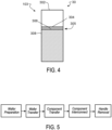
- one or more of the processes described here can be used to position the discrete component 10 on the device substrate 12 such that the active face 102 of the discrete component 10 is oriented toward the device substrate 12 (which we sometimes call a "face-down" position or a "flip-chip” configuration).
- the discrete component can be electrically connected to other components on the device substrate using flip-chip assembly methods such as conductive adhesives or soldering.
- Wafer processing (202) includes fabricating or obtaining wafers bearing large numbers of discrete components fabricated thereon. We sometimes refer to wafer processing as discrete component fabrication. The discrete components are fabricated on the wafers using semiconductor processing techniques such as thin film processing methods on a semiconductor substrate, such as a bulk silicon substrate, a silicon-on-insulator substrate, a germanium substrate, a gallium arsenide substrate, a sapphire substrate, or another type of semiconductor substrate.
- a semiconductor substrate such as a bulk silicon substrate, a silicon-on-insulator substrate, a germanium substrate, a gallium arsenide substrate, a sapphire substrate, or another type of semiconductor substrate.
- Each of the general process steps shown in Fig. 5 can have one or more aspects, one or more of which can be carried out for each specific process described here.
- wafer thinning to a thickness of about 50 ⁇ m can be accomplished by mechanical backside grinding followed by polishing.
- the wafer is temporarily bonded to a support substrate 302, such as a thicker wafer (e.g., the 3M Wafer Support System ® ).
- a support substrate 302 such as a thicker wafer (e.g., the 3M Wafer Support System ® ).
- an active layer 310 on the top surface of the wafer 300, on which the integrated circuitry is formed faces down toward the support substrate 302.
- the thinned wafer is removed from the support substrate 304.
- the second surface 106 includes a pressure-sensitive adhesive and the first surface 104 can include a UV-release material or a thermal-release material.
- exemplary release materials that are compatible with semiconductor materials are known, and selectable based on the desired adhesion characteristics.
- the handle release layer 105 is formed of a material that responds mechanically to an applied stimulus.
- the handle release layer undergoes a mechanical change in response to a stimulus.
- the handle release layer can lose adhesion as a result of a change in surface morphology caused by application of the stimulus.
- Example handle release layers can be formed of materials that transition from smooth and highly adhesive to rough and poorly adhesive responsive to heat, ultraviolet light, or another type of stimulus.
- the handle release layer undergoes a phase transition in response to a stimulus, losing adhesion as a result of a physical change in state. The transition can be from the solid to the liquid phase (melting) or from the solid to the gas phase (sublimation).
- attachment means between the discrete component 10 and the handle substrate 108 is generally described as an adhesive tape, other arrangements would be possible. For example, vacuum or electrostatic forces could be used to form this attachment temporarily.
- the attachment means and characteristics, such as bond strength can be selected such that the bond strength between the discrete component and the substrate is greater than the bond strength between the discrete component and the handle as the discrete component is bonded with the substrate.
- the handle release layer 105 it is desirable to arrange for the handle release layer 105 to be relatively thin, for example to have a thickness less than 20 ⁇ m, preferably less than 10 ⁇ m, and in some cases less than 5 ⁇ m.
- a thin handle release layer enables the use of certain advantageous chip dicing methods and improves chip quality after dicing and transfer to the substrate.
- the use of thicker handle release layers can contribute to die chipping or cracking during the dicing process.
- wafer preparation can include dicing the wafer handle assembly 400 into handle assemblies 500 (sometimes referred to as singulating the wafer), or dicing a wafer without handle substrate into discrete components.
- a wafer handle assembly is a wafer attached to a handle substrate.
- a handle assembly is an individual discrete component attached to a portion of a handle substrate.
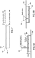
- the wafer handle assembly can be completely or partially diced by dry or wet etching, by plasma dicing, by mechanical sawing (as shown in Fig. 8A ), by laser ablation, by stealth dicing (as shown in Fig. 8B ), or by another dicing technique.
- the wafer handle assembly 400 is diced indirectly by laser micromachining (sometimes referred to as laser stealth dicing) using a laser beam 504 incident on the back side of the wafer handle assembly 400.
- laser micromachining sometimes referred to as laser stealth dicing
- mechanical sawing and laser stealth dicing are used sequentially to completely dice a wafer handle assembly 400.
- the wafer handle assembly 400 including the thinned wafer and the handle substrate can be diced.
- the thinned wafer is not attached to a handle substrate during dicing.
- the wafer handle assembly 400 or the wafer can be adhered to a dicing tape 506 for dicing.
- the dicing tape 506 can have a backing material of polyvinyl chloride (PVC), polyolefin, polyethylene, or another material, and an adhesive surface to which the wafer handle assembly or the wafer is adhered.
- wafer transfer can occur before wafer dicing.
- the wafer handle assembly or the wafer can be mounted on a transparent carrier and the mounted wafer handle assembly or wafer is diced.
- the transparent carrier can be formed of a material, such as glass or a transparent polymer, that is at least partially transparent to at least some wavelengths of the ultraviolet, visible, or infrared electromagnetic spectrum.
- the transparent carrier can have a layer of a dynamic releasing layer (DRL) disposed on a surface thereof, such as described in PCT WO2012/033147 .
- DRL dynamic releasing layer
- the wafer can be partially diced before the wafer transfer process step and dicing can be completed after the wafer transfer process step (described below).
- partially or completely diced handle assemblies or an undiced wafer or wafer handle assembly is transferred from a dicing tape to a transparent carrier or to a die carrier, such as a waffle pack, a gel pack, or another type of carrier.
- a die carrier such as a waffle pack, a gel pack, or another type of carrier.
- Various approaches can be used for wafer transfer, sometimes in combination with dicing processes.
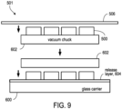
- diced handle assemblies 500 or discrete components are transferred from dicing tape 506 onto the transparent carrier 600 or a die carrier.
- the diced handle assemblies 500 or discrete components are removed from the dicing tape 506, for instance, using suction provided by a vacuum chuck 602.
- a transparent carrier 600 or a die carrier is brought into contact with the diced handle assemblies 500 or undiced wafer or wafer handle assembly that is suctioned onto the vacuum check 602.
- the suction force is removed, causing the handle assemblies 500 or undiced wafer or wafer handle assembly to be transferred onto the transparent carrier 600 or the die carrier.
- diced handle assemblies 500 or discrete components are transferred from dicing tape 506 onto the transparent carrier 600 or a die carrier.
- a wafer or wafer handle assembly is adhered to a dicing tape and diced into handle assemblies 500 or discrete components.
- the dicing tape 506 is formed of a material that undergoes a reduction in adhesion responsive to a stimulus, such as heat or light.
- the dicing tape 506 can be an ultraviolet (UV)-release adhesive that undergoes a reduction in adhesion when exposed to UV light.
- UV dicing tape is exposed to ultraviolet light 508, causing the adhesion between the diced handle assemblies or discrete components to be weakened.
- a vacuum chuck 510 is coated with a material 512 that undergoes a reduction in adhesion responsive to a stimulus, such as heat or light.
- the vacuum chuck 510 can be coated with a thermal release tape 512 (e.g., such as a REVALPHA ® double-coated thermal release tape by Nitto ® ) and a vacuum is drawn to keep the thermal release tape 512 in position.
- the diced handle assemblies 500 or discrete components are removed from the UV dicing tape 506 by contact with the tape-covered vacuum chuck 510.
- the thermal release tape 512 adheres to the diced handle assemblies 500 or discrete components with an adhesion that is greater than the weakened adhesion between the previously exposed UV dicing tape 506 and the diced handle assemblies 500 or discrete components, thus removing the diced handle assemblies 500 or discrete components from the dicing tape 506.
- the dicing tape 506 is peeled off, leaving the handle assemblies 500 or discrete components adhered to the thermal release tape 512.
- a transparent carrier 600 with a dynamic releasing layer disposed thereon is brought into contact with the diced handle assemblies 500 or discrete components adhered to the thermal release tape 512 on the vacuum chuck 510.
- the transparent carrier 600 can be placed on top of the diced handle assemblies 500 or discrete components and weighted for strong contact.
- a positive pressure can be applied to the vacuum chuck 510 to push the thermal release tape 512 away from the chuck 510, thus further pressing the diced handle assemblies or discrete components against the dynamic releasing layer of the transparent carrier 600.
- the stack including the transparent carrier 600, diced handle assemblies 500 or discrete components, and the thermal release tape 512 is removed from the vacuum chuck 510 and heated to a temperature at which the thermal release tape loses some or all of its adhesion (referred to as the characteristic temperature of the thermal release tape).
- the thermal release tape 512 is then peeled off, leaving the diced handle assemblies 500 or discrete components on the transparent carrier 600.
- the wafer transfer approach 320 can be used as long as the characteristic temperature of the thermal release tape is lower than the temperature that causes the handle release layer 105 of the handle assemblies to melt, flow, or degrade. Losses can also be mitigated by providing uniform contact between the discrete components or handle assemblies and the dynamic releasing layer on the transparent carrier, e.g., by providing a flat vacuum chuck and flat surface of the dynamic releasing layer or by providing positive pressure from the vacuum chuck to force a better contact. In some cases, accuracy of placement of discrete components or handle assembles on the transparent carrier can be facilitated by lifting the thermal release tape straight up when removing the thermal release tape.
- a wafer 300 or wafer handle assembly is adhered to the transparent carrier 600 via a material with controllable adhesion 374.
- the material with controllable adhesion 374 includes both the dynamic releasing layer and a UV or thermal release adhesive.
- the wafer 300 or wafer handle assembly is diced (372) directly on the transparent carrier 600.
- the material with controllable adhesion 374 has an adhesion that is strong enough to allow for secure attachment of the wafer 300 or wafer handle assembly to the transparent carrier 600 during dicing.
- the material with controllable adhesion 374 is exposed to a stimulus (376), such as heat or ultraviolet light, causing the adhesion of the material 374 to be reduced.
- a stimulus such as heat or ultraviolet light
- the adhesion level of the material 374 following exposure can be controlled by controlling parameters of the stimulus, such as the exposure intensity (e.g., the intensity of the ultraviolet light or the temperature), exposure time, or other stimulus parameters.
- the adhesion of the material 374 can be reduced to a level compatible with the laser assisted contactless transfer method 800 described below.
- the wafer transfer approach 350 eliminates the component transfer process (discussed below), thus simplifying the process flow. In addition, without a component transfer process, there is no possibility of loss of discrete components or handle assemblies during component transfer, and thus process yield can be improved using the wafer transfer approach 350.
- a wafer or wafer handle assembly 400 is partially diced (552), e.g., using partial blade dicing (as shown), laser dicing, wet etching, or another approach. Partial dicing removes the passivation layer and the metal from the spaces (sometimes called streets) between the discrete components on the wafer or wafer handle assembly 400, leaving a small amount of material (e.g., less than about 20 ⁇ m, such as about 5 ⁇ m, about 10 ⁇ m, about 15 ⁇ m, about 20 ⁇ m, or another amount) at the bottom of each dicing street. Partial dicing facilitates subsequent non-contact dicing such as plasma dicing.
- a wafer transfer approach 570 the wafer or wafer handle assembly 400 is completely diced on dicing tape.
- a two-step dicing process can be used in which the wafer or wafer handle assembly 400 is partially diced with a dicing blade (572) followed by complete dicing using a stealth dicing approach (574).
- the diced discrete components or handle assemblies are transferred (576) to a vacuum chuck covered with a thermal release tape (e.g., Revalpha) and released to a transparent carrier 600 (578) as described above for the wafer transfer approach 320.
- a thermal release tape e.g., Revalpha
- the transparent carrier includes a material with controllable adhesion 580, in addition to or in place of the dynamic releasing layer. Once the diced discrete components are adhered to the transparent carrier, the material with controllable adhesion 580 is exposed to a stimulus (582) as described above for the wafer transfer approach 370 to reduce the adhesion of the material 580 to a level compatible with the laser assisted contactless transfer method 800 described below.
- the wafer transfer approach 570 can achieve lower loss of discrete components or handle assemblies and can enable precise control of the laser assisted contactless transfer method 800 via control of the adhesion level of the material 580.
- pick-and-place tools are used to transfer handle assemblies or discrete components to the transparent carrier.
- the handle assemblies or discrete components can be rearranged on the transparent carrier according to a desired placement, e.g., in a rectangular array, enabling simplification of placement algorithms.
- This approach also allows only "good" handle assemblies or discrete components to be transferred, thus improving downstream yield.
- This wafer transfer approach may be limited to handle assemblies or discrete components having sizes compatible with pick-and-place equipment and can sometimes have low throughput compared to other wafer transfer approaches.
- This wafer transfer approach can be useful in prototyping, e.g., in processes in which individual discrete components are thinned and prepared for laser transfer.
- Some processes described here do not include the wafer transfer process step. For instance, processes in which the wafer is mounted on a transparent carrier prior to dicing do not include the wafer transfer process step.
- the device substrate or the discrete components or both can be provided with an attachment element that promotes attachment, such as adhesion, electrical connection, or both, between the discrete components and the device substrate.
- the attachment element can be a material that is curable responsive to an applied stimulus, such as a material that is thermally curable, curable upon exposure to ultraviolet (UV) light, curable upon exposure to mechanical pressure, or otherwise curable.
- the attachment element can be a conductive material, such as a conductive epoxy, e.g., a conductive paste including metal (e.g., silver) or metal-coated particles in a paste, a solder paste, or another conductive material.
- the attachment element can be a non-conductive material, such as Ablebond 8008NC (Henkel Electronic Materials, Irvine, CA).
- the attachment element can be a film, such as an anisotropic conductive film or a non-conductive die attach film.
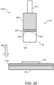
- the pick-and-place approach 700 includes a tool 702 that transfers a handle assembly 500 onto a device substrate 704.
- the tool 702 picks up the handle assembly 500, e.g., by applying a suction to the handle substrate 108 of the handle assembly 500.
- the tool 702 positions the handle assembly 500 directly over an attachment surface 708 on the device substrate 704.
- the tool 702 then moves the handle assembly 500 toward the device substrate 704, for example, in a direction generally show by an arrow 710, until the discrete component 10 contacts the attachment surface 708 on the device substrate 704.
- a laser assisted contactless transfer method 800 which we sometimes call tmSLADT (thermo-mechanical selective laser assisted die transfer).
- the handle assemblies 500 (as shown) or discrete components are adhered to a transparent carrier 600 having a dynamic releasing layer (DRL) 604 disposed thereon, as described above, by an adhesive layer 802.
- the combination of DRL 604 and adhesive layer 802 is sometimes referred to as a carrier release layer.
- the dynamic releasing layer (DRL) 604 is illuminated with light 804 from a laser.
- the DRL 604 absorbs the energy incident thereon from the laser light 804, heating up and partially evaporating, and resulting in formation of a blister 806.
- the blister 806 mechanically pushes the handle assembly 500 onto the attachment surface 708 of the device substrate 704.
- the tmSLADT method is described in PCT WO2012/142177 .
- the adhesion of the adhesive layer 802 is an important parameter in the tmSLADT process 800.
- Fb the force of the expanding blister
- Fa the force of the expanding blister
- the adhesive force between the discrete component or handle assembly and the DRL 604 can be kept at a low level, e.g., just enough to prevent the gravitational force from making the discrete component or handle assembly drop.
- a larger adhesive force to the DRL 604 can be helpful.
- the transfer thus involves a balance between the adhesive forces of the dicing tape and the DRL 604 and the suction force of the transfer device (e.g., the vacuum chuck).
- the wafer transfer approaches described above are operable with various levels of adhesion to the DRL 604, providing flexibility for successful tmSLADT transfer.
- component transfer can include both tmSLADT and pick-and-place approaches.
- discrete components can be transferred to a handle substrate via a tmSLADT approach to form handle assemblies, which can be transferred to the device substrate by a pick-and-place approach.
- handle assemblies can be transferred to a transparent carrier using a pick-and-place approach and then transferred to the device substrate via a tmSLADT approach.
- Discrete components can be transferred onto the device substrate in a face up orientation such that the active face of the discrete components faces up (such as shown in Fig. 1A ), e.g., for wire bonding applications.
- Discrete components can be transferred onto the device substrate in a face down orientation such that the active face of the discrete components faces down (such as shown in Fig. 1B ), e.g., for flip chip assembly.
- a bonding tool applies a stimulus to the attachment element, such as a high temperature, ultraviolet light, mechanical pressure, or another stimulus, or a combination of any two or more of them.
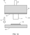
- the bonding tool can apply the stimulus through the discrete component (as shown in Fig. 14 ), through the device substrate, or both.
- the bonding tool is the same tool as the tool that transfers a handle assembly onto the device substrate in the pick-and-place approach to component transfer. The stimulus is removed after a time sufficient to allow the attachment element to cure, forming a mechanical bond, an electrical bond, or both between the discrete components and the device substrate.
- the component interconnection process step can include wire bonding. In some examples, the component interconnection process step can include placing the discrete components onto the device substrate in a face-up configuration and printing a conductive material onto the substrate and the active face of the discrete components.
- the handle substrate is detached from the discrete component and removed, leaving only the discrete component bonded to the device substrate.
- the handle substrate is attached to the discrete component via a handle release layer, which provides adhesion between the discrete component and the handle substrate that can be released responsive to an applied stimulus, such as temperature, ultraviolet light, a normal or shear mechanical force, or another type of stimulus, or a combination of any two or more of them.
- a release tool applies a stimulus to the handle release layer, such as high temperature, ultraviolet light, normal or shear force, or another stimulus, or a combination of any two or more of them.
- the release tool can apply the stimulus through the discrete component, through the device substrate, or both.
- the release tool is the same as the bonding tool that applies a stimulus to the attachment element.
- the stimulus is removed after a time sufficient to allow release of the handle release layer.
- the handle substrate is removed, e.g., by a suction force, by forced air, by an action of the release tool, or in another way.
- a handle substrate is not used, and thus the handle removal process step is not carried out.
- Handle Removal Handle assisted packaging (900) Wafer thinning; To die carrier (optional) Pick-and-place Curing of attachment element Handle detachment and removal Handle attachment; Dicing on dicing tape Laser enabled packaging (150) Wafer thinning; To transparent carrier Laser assisted contactless transfer Curing of attachment element N/A Dicing on dicing tape Direct laser enabled packaging (160) Wafer thinning; N/A Laser assisted contactless transfer Curing of attachment element N/A Dicing on transparent carrier Laser enabled, handle assisted packaging (180) Wafer thinning; To transparent carrier Laser assisted contactless transfer Curing of attachment element Handle detachment and removal Handle attachment; Dicing on dicing tape Direct laser enabled, handle assisted packaging (250) Wafer thinning; N/A Laser assisted contactless transfer Curing of attachment element Handle detachment and removal Handle attachment; Dicing on transparent carrier Handle assisted ultra-small chip assembly (350, 380) Wafer thinning; N/A Laser assisted contactless transfer onto handle; Curing of attachment
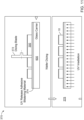
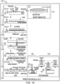
- a process 410 for packaging ultra-small and ultra-thin discrete components can generally include discrete component fabrication (412), wafer preparation (414-422), discrete component transfer (424-430), , discrete component interconnection (430), and handle removal.
- Discrete component transfer in the process 410 includes discrete component transfer onto a handle substrate (424), handle substrate dicing (416426 attachment site preparation (428), and discrete component transfer onto the device substrate (430).
- wafers bearing large numbers of discrete components can be fabricated using known semiconductor techniques such as thin-film methods on a semiconductor material, for example, on a bulk silicon substrates or on layered silicon-insulator-silicon substrates (412).
- Wafer preparation in the process 410 can include partial dicing (404) of the wafer using known semiconductor techniques.
- the discrete components can be partially separated by dry or wet etching, by mechanical sawing (as shown in Fig. 16 ), or by laser micromachining.
- the wafer surface can be protected from damage with a masking film and/or a passivation layer.
- a layer of photoresist, polymers, UV-curable polyimide, laminating films, or another suitable material can be applied and patterned using methods of photolithography or stencil/screen printing.
- the wafer can be thinned to a thickness of approximately 50 ⁇ m using a mechanical grinding technique such as backgrinding.
- a mechanical grinding technique such as backgrinding.
- a noncontact material removal process can be used to reduce the wafer thickness beyond what is achievable by the conventional mechanical grinding process.
- a known noncontact material removal process such as Reactive Ion Etching (RIE), vapor phase etching, or any other appropriate processes can be used to produce the thin wafer.
- the discrete components are formed by the separation of portions of the semiconductor material from the wafer, for example, along the streets formed in the wafer. As shown in Fig. 16 , individual discrete components can be released from the wafer using a dry etching technique, for example, RIE is used (420-422). As described above, the parameters and plasma gas composition are selected such that the silicon in the streets is completely etched or removed (420) prior to etching or removing any other mask material (422). For example, a photoresist material and thickness can be selected, depending on the process parameters and plasma gas compositions if a RIE is used.
- RIE reactive etching
- the parameters and plasma gas composition are selected such that the silicon in the streets is completely etched or removed prior to etching or removing any other mask material.
- process parameters include a 1:1 mix of SF6 and O2 as a plasma gas, pressure 13-14 Pa, power 135 W, and DC-bias 150 V.
- etching continues until the masking layer is completely removed from the discrete component surface.
- Component transfer in the process 410 which includes releasing the individual discrete components from the handling substrate, will depend upon the handling substrate material and/or adhesive material used.
- the discrete components for example, are mounted to a glass interim handle using a DRL layer.
- the discrete components can be released from the DRL using a laser transfer method (424) without contacting the ultra-thin discrete component.
- Other methods than can handle ultra-thin discrete components can be used to transfer the discrete components to the handle substrate.
- component transfer includes both a laser transfer method and pick-and-place.
- the discrete components are transferred from the DRL onto a handle substrate using a laser transfer method.
- the handle substrate provides a larger handle that is compatible in size with a pick-and-place approach to component transfer, thus enabling the handle assemblies to be transferred to the device substrate by a pick-and-place approach.
- the discrete components can be released from the DRL layer and attached to a handle substrate by using a laser contactless technology (424) for ultra-thin chips assembly (which we call tmSLADT), disclosed in PCT WO2012142177 .
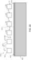
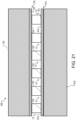
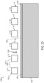
- a distance 508 between each discrete component 10 is selectable based on the capabilities of the wafer dicing tool, for example, kerf and precision, dimensions of the ultra-small and ultra-thin discrete component 10, and dimensions of the handle 108.
- Suitable wafer dicing tools and/or methods include sawing, laser cutting, scribing, stealth dicing, and other known suitable methods.
- the distance 502 is greater than 50 ⁇ m, for example, inclusive of and between 50 ⁇ m and 200 ⁇ m.
- the handle assembly 100 Prior to forming the individual handle assemblies, for example, the handle assembly 100, one or more discrete components 10 are released onto an oversized handle substrate 108a to form an oversized handle assembly 510.
- the oversized handle assembly is positioned below the glass interim handle from which the discrete components are released using the laser transfer method so that when the discrete components are released from the glass interim handle, each discrete component travels in a direction generally indicated by arrow 512 towards a handle release layer 105a, which is pre-coated, for example, using any suitable process such as lamination or spin coating, onto the handle substrate 108a.
- the properties of the handle substrate 108a, the handle release layer 105a including a second surface 106a and a first surface 104a are generally similar to those described with reference to the handle assembly 100, with the exception of the increased size of the handle substrate 108a and associated handle release layer 105a.
- the second surface 106a includes a pressure activated adhesive for attachment of the handle release layer 105a to the handle substrate 108a and the first surface 104a includes a thermal-release surface or a UV release surface, for example, a thermal-release layer or a UV-release layer for attaching the discrete component 10 to the handle release layer 105a.
- the discrete component comes into contact with the handle release layer 105a, the discrete component is releasably attached to the handle substrate 108a, until, for example, an application of heat or UV light.
- the handle release layer 105a is a single layer such that the first surface 104a and the second surface 106a are the same material, for example, a thermal release adhesive or a UV-release adhesive.
- Component transfer in the process 410 includes transferring the handle assemblies 100 onto the device substrate.
- the methods described herein are used to attach ultra-thin and/or ultra-small bare discrete components to any device substrate used in integrated circuit packaging, such as a printed circuit board, plastic casing, ceramic substrate, flexible circuit, or other device substrates.
- attachment means for the discrete component can be provided prior to attaching the discrete components to a device substrate, for example a device substrate 614.
- a thermally cured non-conductive discrete component attachment material such as Ablebond 8008NC by Henkel
- a transfer 610 to a device substrate can include, for example, a discrete component bonding tool 612, a handle assembly 100, and a device substrate 614.
- the discrete component bonding tool 612 attaches to the handle substrate 108 of the handle substrate assembly 100.
- the discrete component bonding tool 612 moves towards the device substrate and positions the discrete component 10 directly over the attachment surface 618 on the device substrate 614.
- the discrete component bonding tool 612 then moves the handle assembly 100 toward the device substrate, for example, in a direction generally show by an arrow 620, until the discrete component 10 contacts the adhesive surface 618. Once contact is made, discrete component interconnection and handle removal are performed.
- the discrete component bonding tool applies a force and temperature profile that can cure the adhesive on the adhesive surface 618. Because the discrete component 10 is attached to the handle substrate assembly through a thermal-release layer, temperature profile delivered to the adhesive on the adhesive surface 618 quickly or simultaneously weakens the adhesion between the discrete components 10 from the handle substrate 108. Any remaining bond strength between the handle substrate 108 and the discrete component 10 is insufficient to overcome the bond strength between the discrete component 10 and the device substrate 614. As a result, the discrete component 10 remains attached to the device surface as the discrete component bonding tool 612 and handle substrate move away from the device substrate. The handle substrate can subsequently be released from the discrete component bonding tool for disposal at a different location by applying a positive pressure through the discrete component bonding tool.
- the transfer means for example, the discrete component bonding tool 612
- the transfer means can be facilitated with a device that is capable of emitting UV light.
- the UV-release discrete component bonding tool can emit UV light with sufficient intensity to de-bond the discrete component from the handle.
- an additional heat source is required to bond the discrete component to the device substrate.
- Such a heat source can be integrated with the work table that holds the device substrate.
- the discrete component can be bonded to the handle substrate by a UV releasable layer while the adhesive on the device substrate can be a UV-cured adhesive material.
- emitting a UV light of a sufficient intensity can weaken the bond between the discrete component and the handle substrate and bond the discrete component to the adhesive on the device substrate.
- thermally sensitive or UV sensitive adhesives are used such that the bond between the discrete component and the handle substrate weakens while the bond between the discrete component and the device substrate strengthens.
- heat or UV light are also or alternatively applied through the device substrate to cure the adhesive on the device substrate.
- transferring the discrete component to a device substrate can include the steps as follows.
- a process 720 for packaging ultra-small and/or ultra-thin discrete components in a face up configuration can generally include obtaining or fabricating a wafer (722), partially dicing the wafer (724), thinning the wafer (726), separating the discrete components from the wafer (728), transfer the discrete components from the wafer to an interim handle substrate (730), transfer the discrete components from the interim handle substrate to the handle substrate (732), bonding the discrete components to the handle substrate while weakening the bond between the interim handle substrate and the discrete components (732), dividing the handle substrate into a plurality of individual handle substrates each including a discrete component (734), preparing the device substrate for attachment with the discrete component (736), picking up the handle assembly using a discrete component bonding tool and positioning the handle assembly over the device substrate to align the discrete component with the attachment adhesive on the device substrate (738), moving the discrete component into contact with the attachment adhesive on the device substrate (738), emitting energy such that the bond between the discrete component
- wafers bearing large numbers of discrete components can be fabricated using known semiconductor techniques such as thin-film methods on a semiconductor material, for example, on bulk silicon substrates or on layered silicon-insulator-silicon substrates (722).
- the wafers can undergo partial dicing using known semiconductor techniques.
- the discrete components can be partially separated by dry or wet etching, by mechanical sawing (as shown in Fig. 19 ), or by laser cutting.
- the wafer is diced to form street depth equal or slightly greater than the final discrete component thickness.
- wafer thinning, discrete component separation are generally similar to the wafer thinning, and discrete component separation described with reference to the process 410 except for any discussion related to a masking film.
- the process 720 omits a masking film so the dry etching (728) is simply carried out until the streets are unobstructed.
- an oversized handle assembly 810 is generally similar to the oversized handle assembly 510, with the exception of the location of the active discrete component face 102 and the type of handle release layer 815.
- the active discrete component face is oriented away from the interim substrate 818.
- the interim substrate 818 is coated with a low-temperature adhesive heat-release tape so that when the tape is exposed to a certain temperature, the tape loses its adhesive properties.
- REVALPHA 319Y-4L by Nitto ® has a release temperature of 90 °C.
- the interim handle substrate 818 is placed over or stacked on the handle substrate 108.
- the handle substrate 108 includes handle release layer 105 including a layer 104 that heat sensitive with a higher release temperature, for example, REVALPHA 319Y-4H by Nitto ® with a release temperature of 150 °C, than the release temperature of the interim handle substrate.
- the stack is heated to a temperature higher than the release temperature of the low-temperature tape but lower than the release temperature of the high-temperature tape. The conditions result in the interim handle substrate 818 losing adhesion.
- the interim handle substrate is freely removable. In some cases, the interim substrate assembly is also reusable.
- heating is a mode of causing the interim handle substrate to lose adhesion
- a variety of techniques can be used for that purpose.
- the handle release layer could be made to lose adhesion by applying a stimulus to cause a change in the surface morphology of the handle release layer.
- the stimulus could be heat or UV light and the corresponding change in the surface morphology of the handle release layer could include formation of small blisters on the surface.
- Such a change in the surface morphology from smooth to blistered will cause a transition of adhesion from sufficiently adhesive to very rough with very low adhesion.
- the material used for the handle release layer can be chosen to respond to such a stimulus by changing its surface morphology.
- the reduction in adhesion is achieved by a phase transition in which the handle release layer loses adhesion by a physical change of state caused by applying a stimulus.
- the phase transition can be from a solid phase to a liquid phase (for example, melting) or from a solid phase to a gas phase (sublimation) or a combination of them.
- the stimulus could be light, heat, pressure, or a combination of any two or more of them.
- the loss of adhesion could be caused by a chemical process.
- chemically triggered loss of adhesion could be based on a change in the chemical structure or composition of the handle release layer or components of it.
- the handle release layer or components of it can be ones that change their chemical structure when exposed to the stimulus.
- the materials can be ones that change their chemical composition (e.g., degrade) when the stimulus is applied.
- Such materials could include: i) materials that undergo thermal decomposition, or thermolysis, which is a chemical decomposition caused by heat, and ii) materials that undergo photodegradation, which is degradation caused by the absorption of light.
- the stimulus for the chemical process could be light or heat or both.
- the release mechanism does not involve melting of the handle release layer material. Release without melting of the handle layer allows the handle substrate to be removed by a vertical motion rather than a lateral sliding motion.
- Vertical removal of the handle substrate can be advantageous, e.g., when the handle substrate is removed by a conventional die bonder. Removal of the handle substrate by a lateral sliding motion can be advantageous in environments such as roll-to-roll assembly lines in which the handle substrate forms part of a continuous web. Release without melting of the handle release layer material can help avoid leaving a residue on the surface of the discrete component after handle removal.
- the handle release layer or the process of reducing its adhesion or both can be selected so that the loss of adhesion is permanent or so that the restoration of adhesion is prevented, inhibited, or delayed.
- This approach has the advantage of reducing or eliminating a time constraint on when the handle must be removed. For instance, such materials may undergo a restoration of adhesion within about 10 seconds, 30 seconds, one minute, 5 minutes, 10 minutes, or another time following reduction of adhesion. Melting a wax, for example, to reduce the adhesion of the handle release layer will leave very little time for removing the handle after the heat that causes the melting of the wax is reduced, because the wax will re-solidify relatively quickly.
- Example materials in which the loss of adhesion is permanent or the restoration of adhesion is prevented, inhibited, or delayed include materials that degrade, decompose, or sublimate; or adhesive tapes such as REVALPHA ® double-coated thermal release tape by Nitto ® .
- the material of the handle release layer or the process of releasing it or both can be selected so that no residue remains on the discrete component after the release.
- materials that leave no residue on the discrete component after the release can include materials that change surface morphology (e.g., such as a REVALPHA ® double-coated thermal release tape by Nitto ® ) or materials that sublimate.
- the discrete component packaging process including preparing the device substrate (736) and transferring the discrete component to the device substrate (738) is generally similar to the discrete component packaging process described with respect to Fig. 16 .
- a process 1000 for packaging ultra-small and ultra-thin discrete components in a flip-chip configuration can generally include obtaining or fabricating a wafer (1002), partially dicing the wafer (1004), thinning the wafer (1006), separating the discrete components from the wafer (1008), transfer the discrete components to a handle substrate (1010) dividing the handle substrate into a plurality of individual handle substrates each including a discrete component (1012), preparing the device substrate for attachment with the discrete component (1014), picking up the handle assembly using a discrete component bonding tool and positioning the handle assembly over the device substrate to align the discrete component with the attachment adhesive on the device substrate (1016), moving the discrete component into contact with the attachment adhesive on the device substrate (1016), emitting energy such that the bond between the discrete component and the handle substrate weakens while the bond between the discrete component and the device substrate strengthens, (1016) moving the discrete component bonding tool away from the device substrate while the discrete component remains bonded to the device substrate, and
- wafers having bumped out discrete components are generally known.
- Common methods for wafer bumping include stud bumping, electroless nickel-gold plating, solder balls, solder paste printing, solder electroplating, etc. While an initial wafer having a low profile electroless nickel-gold plating is compatible with the process described here, the creation of bumps can occur after transferring the discrete components from the glass substrate (1010) and before placing the discrete components on the handle substrate (1012).
- the wafer dicing process (1004), the wafer thinning process (1006), the discrete component separation (1008), the discrete component transfer (1010), forming individual handle substrates (1012), and discrete component bonding (1016) are generally similar to other methods discussed above.
- the discrete components 10 are placed on the handle substrate 108, as shown in Figs. 17 and 23 , in the same manner but for the orientation of the active face 102 on the discrete component 10.
- each of the discrete components 10 are separated by a distance 1202 and travel along a direction 1204.
- the discrete component bonding generally includes picking up the handle assembly using a discrete component bonding tool and positioning the handle assembly over the device substrate to align the discrete component with the attachment adhesive on the device substrate (1016), moving the discrete component into contact with the attachment adhesive on the device substrate (1016), emitting energy such that the bond between the discrete component and the handle substrate weakens while the bond between the discrete component and the device substrate strengthens, (1016) moving the discrete component bonding tool away from the device substrate while the discrete component remains bonded to the device substrate, and releasing the handle substrate from the discrete component bonding tool (1016).
- Wafer preparation in the process 1300 includes wafer thinning, handle attachment, and dicing.
- the wafer is thinned, e.g., to a thickness of less than 50 ⁇ m, such as a thickness of about 25 ⁇ m.
- the wafer can be thinned using a mechanical thinning process or a mechanical thinning process followed by a non-contact thinning process (1304).
- the ultra-thin wafer is mounted to a handle substrate (1306).
- the back side of the wafer is bonded to a 350 ⁇ m thick handle substrate via a 20 ⁇ m thick handle release layer, leaving the active layer of the wafer exposed.
- the active layer of the wafer can be bonded to the handle substrate, leaving the back side of the wafer exposed.
- the process 150 can have advantages. For instance, the use of the laser assisted contactless transfer method to perform component transfer allows the process to be applied to the transfer of a wide range of sizes and types of components, such as components that are too small for a pick-and-place approach or components that are unsuited to be mounted on a handle substrate.
- the process 150 can operate with a higher throughput than other processes that are not laser assisted, because the laser can be electronically scanned to rapidly transfer successive discrete components with little or no realignment of the transparent carrier.
- a laser enabled packaging process (160) enables packaging of ultra-small discrete components without use of a handle substrate.
- a wafer bearing large numbers of discrete components is fabricated or obtained (162).
- discrete component interconnection is performed while the discrete components are still attached to the associated portion of the handle substrate.
- the thick assembly of a discrete component and a handle substrate is less prone to cracking during curing of the attachment element on the device substrate (e.g., during curing of a conductive epoxy) during discrete component interconnection than is a discrete component that is not mounted on a handle substrate.
- a laser enabled, handle assisted packaging process 250 enables packaging of ultra-thin discrete component.
- a wafer bearing large numbers of discrete components is fabricated or obtained (252).
- the back side of the wafer is bonded to a 350 ⁇ m thick handle substrate via a 20 ⁇ m thick handle release layer, leaving the active layer of the wafer exposed.
- the active layer of the wafer can be bonded to the handle substrate, leaving the back side of the wafer exposed.
- Component transfer in process 250 includes releasing the discrete components from the transparent carrier (264) using the laser assisted contactless transfer method described above.
- the discrete components are transferred onto a device substrate having attachment element formed thereon.
- Discrete component interconnection (266) and handle removal (268) are performed by applying pressure, temperature, or ultraviolet light as described above.
- the use of the laser assisted contactless transfer method to perform component transfer allows the process to be applied to the transfer of a wide range of sizes and types of components, such as components that are too thin for a pick-and-place approach.
- the process 250 can have advantages. For instance, the process 250 has a simplified process flow relative to other laser assisted processes by the elimination of the diced wafer transfer step.
- the process yield can be improved because there is no opportunity for die loss during transfer of diced discrete components.
- the possibility of die shifting or rotating with respect to their original positions in the wafer during transfer of the diced discrete components is eliminated because the wafer is transferred as an intact unit.
- the process 1500 can then generally include picking up (1502) the handle assembly 1552 (which includes the discrete component 1501, the handle substrate 108, the handle release layer 105) by applying a vacuum 1513 through a vacuum tube 1516 of a discrete component transfer tool 1508.
- the transfer tool with the handle assemble is then positioned (1502) over the location 1515 of the device substrate as also shown in Figs. 25 and 26 , aligning the discrete component with the attachment adhesive on the device substrate 1502 (614 in Fig. 18 ).
- the discrete component is then moved into contact with the attachment adhesive 1505 (618 in Fig. 18 ) on the device substrate 1502.
- the vacuum in the vacuum tube can be broken to release the transfer tool 1508 from the handle and the transfer tool can be moved away. Then a separate discrete component bonding tool 1510 may be moved into contact with the discrete component.
- Pressure 1550 or energy 1551 e.g., thermal or UV energy, or both
- Pressure 1550 or energy 1551 then can be applied 1517 to the discrete component 1501, the handle substrate 108, the handle release layer 105 through a contact surface 1519 of the bonding tool 1510 into the handle and also through the handle to the bond 1521, through the bond to the discrete component 1501, and through the discrete component 1501 to the bond 1523 with the device substrate.
- the pressure or energy or both can simultaneously or in sequence cause the bond 1521 between the discrete component and the handle substrate to weaken and the bond 1523 between the discrete component and the device substrate to strengthen (1504).
- the pressure can operate simultaneously to weaken the bond 1521 and to strengthen the bond 1523.
- energy in some cases, the energy must flow through the successive elements of the system so that the weakening of bond 1521 may begin or be completed before the strengthening of the bond 1523 begins or is completed, or the weakening and the strengthening can occur in sequence.
- the handle release layer 105 and the attachment adhesive are selected such that the bond 1523 between the discrete component 1501 and the device substrate 1502 forms before the bond 1521 is formed between the handle and the discrete component 1501, or the formation of the bond 1523 and the bond 1521 can occur simultaneously with complete overlap in time, or the formation can overlap partly with either the bond 1523 or the bond 1521 partly occurring earlier than or later than the overlapping period.
- the formation of either the bond 1523 or the bond 1521 can include a hardening or softening of a material, e.g., a wax material.
- the handle release layer 105, the attachment adhesive 1505, or both the handle release layer 105 and the attachment adhesive 1505 may include one or more materials that soften or harden in response to an application of energy.
- the softening of the bond 1523 can occur before the hardening of the bond 1521, or the softening of the bond 1523 can occur after the hardening of the bond 1521, or the two events can occur simultaneously with complete overlap in time, or they can overlap but one or the other can partly occur earlier than or later than the overlapping period.
- the discrete component bonding tool 1510 may be removed leaving the handle assembly (including the discrete component 1501, the handle substrate 108, the handle release layer 105) in contact with the discrete component, which is bonded to the device substrate 1502. While not bonded to the discrete component (because of the weakening of bond 1523), the handle remains in contact with the discrete component, for example, due to gravitational force, surface attraction force, or residual adhesive force remaining after the debonding process, or a combination of two or more of these forces the two.
- the handle substrate may then be removed (1506) from the discrete component using any of a variety of separation techniques, e.g., brushing, compressed air, vacuum, vibration, liquid jet, electrostatic, electromagnetic force reorienting the device substrate such that gravity separates the handle from the discrete component, or any combination of two or more of those.
- separation techniques e.g., brushing, compressed air, vacuum, vibration, liquid jet, electrostatic, electromagnetic force reorienting the device substrate such that gravity separates the handle from the discrete component, or any combination of two or more of those.
- separation techniques e.g., brushing, compressed air, vacuum, vibration, liquid jet, electrostatic, electromagnetic force reorienting the device substrate such that gravity separates the handle from the discrete component, or any combination of two or more of those.
- separation techniques e.g., techniques applying force, energy, contact, and any combination of two or more of these to separate the handle substrate from the discrete component so long as the discrete component and/or the handle substrate are not damaged.
- the discrete transfer tool 1508 may be configured to apply a vacuum force to the handle assembly similarly to the use of the discrete component transfer tool 612 in Fig. 18 . In some examples, the discrete transfer tool 1508 may be configured to apply pressure, heat, or UV light, or a combination of them to the handle assembly similarly to use of the discrete component transfer tool 602 in Fig. 18 .
- Fig. 31 shows the removal of one handle assembly; the same separation technique or techniques may be used to remove two or more handle assemblies at the same time.
- multiple handle substrates may be arranged in proximity to each other such that a brush, a blade, an application of compressed air, an application of a vacuum, or an application of a vibrational force, or any combination of two or more of them, may remove the two or more handle assemblies from their corresponding discrete components.
- one or more of the processes described here can be used to position thin discrete components onto a device substrate starting from individual discrete components with regular thickness rather than starting from a wafer.
- Processes starting from individual discrete components can be used to place multiple, different discrete components on a single device substrate.
- the pick-and-place approach or the laser assisted contactless transfer method can be used to position individual discrete components in target positions in the device substrate.
- the device substrate can remain stationary and each discrete component can be moved relative to the device substrate until its target position is reached.
- the device substrate can be moved relative to the discrete components until the target position for a particular discrete component is positioned under that discrete component.
- the ability to place multiple, different discrete components onto a single substrate can have applications in research and development, for instance, in order to facilitate testing of multiple types of discrete components.
- individual discrete components 452 are received and mounted (440) on a first handle substrate 454 via a handle release layer 456.
- the discrete components 452 can be mounted onto the first handle substrate 454 by a pick-and-place approach or another method for positioning discrete components.
- the discrete components can be of various sizes and thicknesses that are compatible with a pick-and-place approach.
- a second handle substrate 456 having a handle release layer 458 and a layer of flowable material 460 disposed thereon is brought into contact (441) with the discrete components 452 on the first handle substrate 454.
- flowable material broadly to include, for example, any material that has a viscosity that enables the flowable material to flow responsive to a stimulus, such as pressure and vacuum lamination applied when the second handle substrate 456 is brought into contact with the discrete components 452 on the first handle substrate 454.
- Example flowable materials can include materials that undergo a phase change from liquid to solid responsive to application of a stimulus such as heat or light (e.g., ultraviolet light).
Landscapes
- Engineering & Computer Science (AREA)
- Mechanical Engineering (AREA)
- Container, Conveyance, Adherence, Positioning, Of Wafer (AREA)
- Dicing (AREA)
- Wire Bonding (AREA)
- Die Bonding (AREA)
- Physics & Mathematics (AREA)
- Plasma & Fusion (AREA)
- Fixed Capacitors And Capacitor Manufacturing Machines (AREA)
- Electron Tubes For Measurement (AREA)
- Packaging Of Annular Or Rod-Shaped Articles, Wearing Apparel, Cassettes, Or The Like (AREA)
Claims (8)
- Procédé (800) comprenant :le découpage d'une tranche (300) fixée à une couche de libération disposée sur un support transparent (600) pour former des composants discrets (500), la couche de libération comprenant une couche d'adhésif (802) et une couche de libération dynamique (604), le support transparent étant transparent à un premier et un deuxième stimulus (376, 804) ;l'acheminement du premier stimulus (376) à travers le support transparent pour exposer la couche de libération au premier stimulus (376), une adhérence entre la couche d'adhésif et les composants discrets (500) étant réduite en réponse au premier stimulus (376) depuis un premier niveau d'adhérence suffisamment fort pour permettre une fixation sûre de la tranche au support transparent pendant le découpage jusqu'à un deuxième niveau d'adhérence suffisamment grand pour maintenir le composant discret en place, mais suffisamment petit pour permettre un transfert ultérieur à un substrat de dispositif (704) au moyen du deuxième stimulus ; etl'acheminement du deuxième stimulus (804) sous la forme de lumière laser à travers le support transparent pour exposer la couche de libération au deuxième stimulus (804), la couche de libération dynamique (604) répondant en absorbant l'énergie lui parvenant depuis le deuxième stimulus (804), s'échauffant et s'évaporant partiellement, ce qui aboutit à la formation d'une boursouflure (806), la boursouflure poussant mécaniquement les composants discrets (500) pour les transférer à un substrat de dispositif (704).
- Procédé (800) de la revendication 1, dans lequel l'exposition de la couche de libération à un stimulus (804) comprend l'exposition de la couche de libération à de la chaleur.
- Procédé (800) de la revendication 1 ou 2, dans lequel l'exposition de la couche de libération à un stimulus (804) comprend l'exposition de la couche de libération à un rayonnement ultraviolet.
- Procédé (800) de l'une quelconque des revendications 1 à 3, dans lequel le découpage de la tranche comprend le découpage d'un ensemble de manipulation de tranche pour former des ensembles de manipulation, l'ensemble de manipulation de tranche comprenant une tranche fixée à un substrat de manipulation, chaque ensemble de manipulation comprenant un des composants discrets (500) et une partie correspondante du substrat de manipulation.
- Procédé (800) de la revendication 4, dans lequel le substrat de manipulation comporte n'importe quel substrat rigide d'une épaisseur et/ou d'une rigidité dépassant l'épaisseur et/ou la rigidité des composants discrets (500) pour une utilisation temporaire pour transférer les composants discrets (500) au substrat de dispositif (704).
- Procédé (800) de la revendication 5, dans lequel le substrat rigide comporte des tranches de silicium vierges, des substrat de verre ou de céramique, ou des substrats constitués de polymères rigides ou de matériaux composites.
- Procédé (800) de l'une quelconque des revendications 1 à 6, dans lequel le support transparent (600) comporte n'importe quel matériau auquel les composants discrets (500) sont fixés par le biais de la couche de libération et qui est au moins partiellement transparent à au moins certaines longueurs d'onde du spectre électromagnétique ultraviolet, visible ou infrarouge.
- Procédé (800) de la revendication 7, dans lequel le matériau comporte du verre ou un polymère transparent.
Priority Applications (1)
| Application Number | Priority Date | Filing Date | Title |
|---|---|---|---|
| EP23218338.4A EP4360877A3 (fr) | 2016-01-15 | 2017-01-12 | Placement de composants discrets ultra-petits ou ultra-fins |
Applications Claiming Priority (2)
| Application Number | Priority Date | Filing Date | Title |
|---|---|---|---|
| US201662279143P | 2016-01-15 | 2016-01-15 | |
| PCT/US2017/013216 WO2017123780A1 (fr) | 2016-01-15 | 2017-01-12 | Placement de composants discrets ultra-petits ou ultra-fins |
Related Child Applications (1)
| Application Number | Title | Priority Date | Filing Date |
|---|---|---|---|
| EP23218338.4A Division EP4360877A3 (fr) | 2016-01-15 | 2017-01-12 | Placement de composants discrets ultra-petits ou ultra-fins |
Publications (3)
| Publication Number | Publication Date |
|---|---|
| EP3402676A1 EP3402676A1 (fr) | 2018-11-21 |
| EP3402676A4 EP3402676A4 (fr) | 2019-09-11 |
| EP3402676B1 true EP3402676B1 (fr) | 2023-12-20 |
Family
ID=59311412
Family Applications (2)
| Application Number | Title | Priority Date | Filing Date |
|---|---|---|---|
| EP23218338.4A Pending EP4360877A3 (fr) | 2016-01-15 | 2017-01-12 | Placement de composants discrets ultra-petits ou ultra-fins |
| EP17738950.9A Active EP3402676B1 (fr) | 2016-01-15 | 2017-01-12 | Placement de composants discrets ultra-petits ou ultra-fins |
Family Applications Before (1)
| Application Number | Title | Priority Date | Filing Date |
|---|---|---|---|
| EP23218338.4A Pending EP4360877A3 (fr) | 2016-01-15 | 2017-01-12 | Placement de composants discrets ultra-petits ou ultra-fins |
Country Status (7)
| Country | Link |
|---|---|
| US (1) | US10748802B2 (fr) |
| EP (2) | EP4360877A3 (fr) |
| JP (4) | JP6759343B2 (fr) |
| KR (4) | KR102915552B1 (fr) |
| CN (2) | CN108778737B (fr) |
| TW (3) | TWI889995B (fr) |
| WO (1) | WO2017123780A1 (fr) |
Families Citing this family (39)
| Publication number | Priority date | Publication date | Assignee | Title |
|---|---|---|---|---|
| US9929121B2 (en) * | 2015-08-31 | 2018-03-27 | Kulicke And Soffa Industries, Inc. | Bonding machines for bonding semiconductor elements, methods of operating bonding machines, and techniques for improving UPH on such bonding machines |
| US12094811B2 (en) | 2016-04-29 | 2024-09-17 | Kulicke And Soffa Industries, Inc. | Connecting electronic components to substrates |
| US11201077B2 (en) | 2017-06-12 | 2021-12-14 | Kulicke & Soffa Netherlands B.V. | Parallel assembly of discrete components onto a substrate |
| KR20240130146A (ko) | 2017-06-12 | 2024-08-28 | 쿨리케 & 소파 네덜란드 비.브이. | 개별 부품들의 기판 상으로의 병렬적 조립 |
| DE102017130929A1 (de) * | 2017-12-21 | 2019-06-27 | RF360 Europe GmbH | Verfahren zum Produzieren einer funktionalen Dünnfilmschicht |
| CN109994413A (zh) * | 2017-12-29 | 2019-07-09 | 南昌欧菲显示科技有限公司 | 微型元件巨量转移方法 |
| KR102563929B1 (ko) * | 2018-03-09 | 2023-08-04 | 삼성전자주식회사 | 반도체 다이들의 개별화 방법 및 반도체 패키지의 제조 방법 |
| TWI878222B (zh) | 2018-05-14 | 2025-04-01 | 晶元光電股份有限公司 | 一種發光裝置及其製造方法 |
| WO2019227955A1 (fr) | 2018-05-31 | 2019-12-05 | 浙江清华柔性电子技术研究院 | Dispositif de transition pour dispositif flexible et son procédé de préparation, et procédé de fabrication pour dispositif flexible |
| JP7147847B2 (ja) * | 2018-07-25 | 2022-10-05 | 株式会社ニコン | 接合方法および接合装置 |
| US10818551B2 (en) * | 2019-01-09 | 2020-10-27 | Semiconductor Components Industries, Llc | Plasma die singulation systems and related methods |
| CN121335436A (zh) | 2019-02-15 | 2026-01-13 | 库力索法荷兰有限公司 | 用于组装离散组件的动态释放带 |
| CN114667597A (zh) * | 2019-06-11 | 2022-06-24 | 库力索法荷兰有限公司 | 在分立部件的组装中用于位置误差补偿的材料 |
| KR102800734B1 (ko) | 2019-07-04 | 2025-04-29 | 삼성전자주식회사 | 마이크로 led 디스플레이 모듈 및 이를 제조하는 방법 |
| DE102019120955B8 (de) | 2019-08-02 | 2021-03-18 | Asm Amicra Microtechnologies Gmbh | Bondtool, Bondvorrichtung und Bondverfahren |
| EP3799112B1 (fr) * | 2019-09-30 | 2024-02-21 | IMEC vzw | Procédé de découpage d'un substrat semiconducteur en une pluralité de matrices |
| US11302561B2 (en) * | 2019-11-12 | 2022-04-12 | Palo Alto Research Center Incorporated | Transfer elements that selectably hold and release objects based on changes in stiffness |
| KR102279643B1 (ko) * | 2019-11-15 | 2021-07-20 | 한국기계연구원 | 캐리어 기판 및 이를 이용한 소자 전사방법 |
| WO2021126580A1 (fr) * | 2019-12-17 | 2021-06-24 | Uniqarta, Inc. | Bandes adhésives destinées à recevoir des composants discrets |
| DE102019134756A1 (de) * | 2019-12-17 | 2021-06-17 | OSRAM Opto Semiconductors Gesellschaft mit beschränkter Haftung | Verfahren zur herstellung einer beleuchtungsvorrichtung |
| CN111599912B (zh) * | 2020-06-01 | 2020-11-24 | 广东工业大学 | 一种柔性可拉伸的Micro-LED巨量转移装置和方法 |
| EP3933902B1 (fr) * | 2020-06-29 | 2023-05-03 | IMEC vzw | Procédé de positionnement de composants sur un substrat |
| WO2022063431A1 (fr) | 2020-09-22 | 2022-03-31 | Kulicke & Soffa Netherlands B.V. | Matériaux de capture de puces réutilisables, matériaux de libération de puces réutilisables, systèmes de transfert de puces associés, et leurs procédés d'utilisation |
| JP7705240B2 (ja) * | 2020-12-08 | 2025-07-09 | リンテック株式会社 | 保持方法および保持装置 |
| JP7783901B2 (ja) * | 2021-03-02 | 2025-12-10 | ネーデルランドセ・オルガニサティ・フォール・トゥーヘパスト-ナトゥールウェテンスハッペライク・オンデルズーク・テーエヌオー | 構成部品の光誘起移動用の多層解放スタック |
| JP6978129B1 (ja) * | 2021-03-18 | 2021-12-08 | 株式会社写真化学 | デバイスチップの移載機構 |
| EP4315401A4 (fr) * | 2021-03-29 | 2025-11-05 | Univ Texas | Procédés et applications pour gravure chimique influencée par un catalyseur |
| WO2023044308A1 (fr) * | 2021-09-14 | 2023-03-23 | Adeia Semiconductor Bonding Technologies Inc. | Procédé de liaison de substrats minces |
| US12482679B2 (en) | 2021-10-01 | 2025-11-25 | Kulicke And Soffa Industries, Inc. | Methods of transferring a die from a carrier to a receive substrate, and related systems and materials |
| US12596306B2 (en) * | 2021-11-11 | 2026-04-07 | Terecircuits Corporation | Photochemical and thermal release layer processes and uses in device manufacturing |
| JP2023144223A (ja) * | 2022-03-28 | 2023-10-11 | 東レエンジニアリング株式会社 | 転写装置および転写方法 |
| JP2023144203A (ja) * | 2022-03-28 | 2023-10-11 | 東レエンジニアリング株式会社 | 接合装置および接合方法 |
| CN114743916B (zh) * | 2022-03-31 | 2025-11-28 | Tcl华星光电技术有限公司 | 转移装置及转移方法 |
| JP2024058321A (ja) * | 2022-10-14 | 2024-04-25 | 株式会社ディスコ | ウエーハの加工方法 |
| EP4358121A1 (fr) * | 2022-10-18 | 2024-04-24 | Nederlandse Organisatie voor toegepast-natuurwetenschappelijk Onderzoek TNO | Procédé et dispositif pour déposer des composants sur une surface cible d'une cible ainsi que plaque donneuse destinée à être utilisée avec ceux-ci |
| US20240371818A1 (en) * | 2023-05-01 | 2024-11-07 | Taiwan Semiconductor Manufacturing Co., Ltd. | Edge fill for stacked structure |
| WO2025105196A1 (fr) * | 2023-11-13 | 2025-05-22 | デクセリアルズ株式会社 | Procédé de production de film individualisé, film individualisé, procédé de production de structure de connexion et structure de connexion |
| WO2025109895A1 (fr) * | 2023-11-21 | 2025-05-30 | パナソニックIpマネジメント株式会社 | Procédé de transcription d'élément et dispositif de transcription d'élément |
| WO2025204883A1 (fr) * | 2024-03-26 | 2025-10-02 | 東レエンジニアリング株式会社 | Système de fabrication de dispositif et procédé de fabrication de dispositif |
Family Cites Families (19)
| Publication number | Priority date | Publication date | Assignee | Title |
|---|---|---|---|---|
| WO2002084631A1 (fr) * | 2001-04-11 | 2002-10-24 | Sony Corporation | Procede de transfert d'element, procede de disposition d'element mettant en oeuvre ce procede et procede de production d'un appareil d'affichage d'image |
| JP4137471B2 (ja) * | 2002-03-04 | 2008-08-20 | 東京エレクトロン株式会社 | ダイシング方法、集積回路チップの検査方法及び基板保持装置 |
| JP5964005B2 (ja) * | 2005-04-08 | 2016-08-03 | パック テック−パッケージング テクノロジーズ ゲーエムベーハー | チップを接触基板に移送する方法及び装置 |
| JP4781874B2 (ja) * | 2006-03-30 | 2011-09-28 | 東京応化工業株式会社 | サポートプレートの剥離方法 |
| US20080003780A1 (en) * | 2006-06-30 | 2008-01-03 | Haixiao Sun | Detachable stiffener for ultra-thin die |
| CN102015943A (zh) * | 2008-03-07 | 2011-04-13 | 3M创新有限公司 | 具有图案化背衬的切割带和晶粒附连粘合剂 |
| TWI472882B (zh) * | 2008-05-06 | 2015-02-11 | 諾菲勒斯系統公司 | 光阻剝離方法及設備 |
| US7741567B2 (en) * | 2008-05-19 | 2010-06-22 | Texas Instruments Incorporated | Integrated circuit package having integrated faraday shield |
| US20100072490A1 (en) * | 2008-09-24 | 2010-03-25 | Kerr Roger S | Low cost flexible display sheet |
| WO2012033147A1 (fr) | 2010-09-09 | 2012-03-15 | 学校法人 東北学院 | Capteur de concentration de gaz spécifié |
| EP2434528A1 (fr) * | 2010-09-28 | 2012-03-28 | Nederlandse Organisatie voor toegepast -natuurwetenschappelijk onderzoek TNO | Support actif pour le transport d'une tranche et procédé de libération |
| JP6053756B2 (ja) | 2011-04-11 | 2016-12-27 | エヌディーエスユー リサーチ ファウンデーション | レーザで促進される、分離した部品の選択的な転写 |
| US8409927B1 (en) * | 2011-09-23 | 2013-04-02 | GlobalFoundries, Inc. | Methods for fabricating integrated circuit systems including high reliability die under-fill |
| US8969177B2 (en) * | 2012-06-29 | 2015-03-03 | Applied Materials, Inc. | Laser and plasma etch wafer dicing with a double sided UV-curable adhesive film |
| US10741718B2 (en) * | 2012-09-05 | 2020-08-11 | Lumileds, LLC | Laser de-bond carrier wafer from device wafer |
| KR20150085518A (ko) * | 2012-11-09 | 2015-07-23 | 쓰리엠 이노베이티브 프로퍼티즈 컴파니 | 열 계면 조성물 및 이의 제조방법 및 사용 방법 |
| US9136782B2 (en) * | 2013-07-02 | 2015-09-15 | The Boeing Company | Motor control for stability and power supply protection |
| CN107107600B (zh) * | 2014-08-05 | 2021-07-27 | 尤尼卡尔塔股份有限公司 | 设置便于组装的超小或超薄分立元件 |
| US9929121B2 (en) * | 2015-08-31 | 2018-03-27 | Kulicke And Soffa Industries, Inc. | Bonding machines for bonding semiconductor elements, methods of operating bonding machines, and techniques for improving UPH on such bonding machines |
-
2016
- 2016-01-25 TW TW111124992A patent/TWI889995B/zh active
- 2016-01-25 TW TW105102254A patent/TWI783910B/zh active
- 2016-01-25 TW TW114106764A patent/TW202524641A/zh unknown
-
2017
- 2017-01-12 EP EP23218338.4A patent/EP4360877A3/fr active Pending
- 2017-01-12 KR KR1020237025649A patent/KR102915552B1/ko active Active
- 2017-01-12 KR KR1020257017942A patent/KR20250088638A/ko active Pending
- 2017-01-12 US US16/069,801 patent/US10748802B2/en active Active
- 2017-01-12 EP EP17738950.9A patent/EP3402676B1/fr active Active
- 2017-01-12 CN CN201780017238.7A patent/CN108778737B/zh active Active
- 2017-01-12 JP JP2018536735A patent/JP6759343B2/ja active Active
- 2017-01-12 KR KR1020217000730A patent/KR102561688B1/ko active Active
- 2017-01-12 CN CN202111319183.XA patent/CN114188275A/zh active Pending
- 2017-01-12 KR KR1020187023450A patent/KR102203790B1/ko active Active
- 2017-01-12 WO PCT/US2017/013216 patent/WO2017123780A1/fr not_active Ceased
-
2020
- 2020-09-01 JP JP2020146643A patent/JP7390996B2/ja active Active
-
2022
- 2022-10-06 JP JP2022161795A patent/JP7566838B2/ja active Active
-
2024
- 2024-10-02 JP JP2024173256A patent/JP2025013342A/ja active Pending
Also Published As
| Publication number | Publication date |
|---|---|
| KR20230118701A (ko) | 2023-08-11 |
| EP4360877A2 (fr) | 2024-05-01 |
| TW201725642A (zh) | 2017-07-16 |
| JP2020194980A (ja) | 2020-12-03 |
| EP3402676A4 (fr) | 2019-09-11 |
| JP2025013342A (ja) | 2025-01-24 |
| JP6759343B2 (ja) | 2020-09-23 |
| KR20180101541A (ko) | 2018-09-12 |
| JP7390996B2 (ja) | 2023-12-04 |
| CN114188275A (zh) | 2022-03-15 |
| EP3402676A1 (fr) | 2018-11-21 |
| WO2017123780A1 (fr) | 2017-07-20 |
| KR102915552B1 (ko) | 2026-01-22 |
| US20190057891A1 (en) | 2019-02-21 |
| US10748802B2 (en) | 2020-08-18 |
| TW202524641A (zh) | 2025-06-16 |
| TWI783910B (zh) | 2022-11-21 |
| KR20210007037A (ko) | 2021-01-19 |
| JP7566838B2 (ja) | 2024-10-15 |
| CN108778737A (zh) | 2018-11-09 |
| JP2019503081A (ja) | 2019-01-31 |
| KR102561688B1 (ko) | 2023-07-31 |
| KR102203790B1 (ko) | 2021-01-18 |
| EP4360877A3 (fr) | 2025-01-01 |
| TWI889995B (zh) | 2025-07-11 |
| KR20250088638A (ko) | 2025-06-17 |
| TW202308015A (zh) | 2023-02-16 |
| CN108778737B (zh) | 2021-11-26 |
| JP2023010701A (ja) | 2023-01-20 |
Similar Documents
| Publication | Publication Date | Title |
|---|---|---|
| EP3402676B1 (fr) | Placement de composants discrets ultra-petits ou ultra-fins | |
| US12412772B2 (en) | Setting up ultra-small or ultra-thin discrete components for easy assembly | |
| US7022546B2 (en) | Method and device for protecting micro electromechanical systems structures during dicing of a wafer |
Legal Events
| Date | Code | Title | Description |
|---|---|---|---|
| STAA | Information on the status of an ep patent application or granted ep patent |
Free format text: STATUS: THE INTERNATIONAL PUBLICATION HAS BEEN MADE |
|
| PUAI | Public reference made under article 153(3) epc to a published international application that has entered the european phase |
Free format text: ORIGINAL CODE: 0009012 |
|
| STAA | Information on the status of an ep patent application or granted ep patent |
Free format text: STATUS: REQUEST FOR EXAMINATION WAS MADE |
|
| 17P | Request for examination filed |
Effective date: 20180814 |
|
| AK | Designated contracting states |
Kind code of ref document: A1 Designated state(s): AL AT BE BG CH CY CZ DE DK EE ES FI FR GB GR HR HU IE IS IT LI LT LU LV MC MK MT NL NO PL PT RO RS SE SI SK SM TR |
|
| AX | Request for extension of the european patent |
Extension state: BA ME |
|
| DAV | Request for validation of the european patent (deleted) | ||
| DAX | Request for extension of the european patent (deleted) | ||
| A4 | Supplementary search report drawn up and despatched |
Effective date: 20190813 |
|
| RIC1 | Information provided on ipc code assigned before grant |
Ipc: B32B 37/02 20060101AFI20190807BHEP Ipc: B32B 37/26 20060101ALI20190807BHEP Ipc: H01L 21/67 20060101ALI20190807BHEP Ipc: B32B 38/00 20060101ALI20190807BHEP Ipc: H01L 23/488 20060101ALN20190807BHEP Ipc: B32B 38/18 20060101ALN20190807BHEP Ipc: H01L 21/683 20060101ALI20190807BHEP Ipc: B32B 37/00 20060101ALI20190807BHEP Ipc: H01L 21/60 20060101ALI20190807BHEP |
|
| STAA | Information on the status of an ep patent application or granted ep patent |
Free format text: STATUS: EXAMINATION IS IN PROGRESS |
|
| 17Q | First examination report despatched |
Effective date: 20210302 |
|
| RAP1 | Party data changed (applicant data changed or rights of an application transferred) |
Owner name: KULICKE AND SOFFA INDUSTRIES, INC. |
|
| RAP1 | Party data changed (applicant data changed or rights of an application transferred) |
Owner name: KULICKE & SOFFA NETHERLANDS B.V. |
|
| GRAP | Despatch of communication of intention to grant a patent |
Free format text: ORIGINAL CODE: EPIDOSNIGR1 |
|
| STAA | Information on the status of an ep patent application or granted ep patent |
Free format text: STATUS: GRANT OF PATENT IS INTENDED |
|
| RIC1 | Information provided on ipc code assigned before grant |
Ipc: B32B 38/18 20060101ALN20230620BHEP Ipc: H01L 23/488 20060101ALN20230620BHEP Ipc: B32B 37/00 20060101ALI20230620BHEP Ipc: H01L 21/60 20060101ALI20230620BHEP Ipc: H01L 21/683 20060101ALI20230620BHEP Ipc: B32B 38/00 20060101ALI20230620BHEP Ipc: H01L 21/67 20060101ALI20230620BHEP Ipc: B32B 37/26 20060101ALI20230620BHEP Ipc: B32B 37/02 20060101AFI20230620BHEP |
|
| RIC1 | Information provided on ipc code assigned before grant |
Ipc: B32B 38/18 20060101ALN20230627BHEP Ipc: H01L 23/488 20060101ALN20230627BHEP Ipc: B32B 37/00 20060101ALI20230627BHEP Ipc: H01L 21/60 20060101ALI20230627BHEP Ipc: H01L 21/683 20060101ALI20230627BHEP Ipc: B32B 38/00 20060101ALI20230627BHEP Ipc: H01L 21/67 20060101ALI20230627BHEP Ipc: B32B 37/26 20060101ALI20230627BHEP Ipc: B32B 37/02 20060101AFI20230627BHEP |
|
| INTG | Intention to grant announced |
Effective date: 20230713 |
|
| GRAS | Grant fee paid |
Free format text: ORIGINAL CODE: EPIDOSNIGR3 |
|
| GRAA | (expected) grant |
Free format text: ORIGINAL CODE: 0009210 |
|
| STAA | Information on the status of an ep patent application or granted ep patent |
Free format text: STATUS: THE PATENT HAS BEEN GRANTED |
|
| AK | Designated contracting states |
Kind code of ref document: B1 Designated state(s): AL AT BE BG CH CY CZ DE DK EE ES FI FR GB GR HR HU IE IS IT LI LT LU LV MC MK MT NL NO PL PT RO RS SE SI SK SM TR |
|
| REG | Reference to a national code |
Ref country code: GB Ref legal event code: FG4D |
|
| REG | Reference to a national code |
Ref country code: CH Ref legal event code: EP |
|
| REG | Reference to a national code |
Ref country code: DE Ref legal event code: R096 Ref document number: 602017077689 Country of ref document: DE |
|
| REG | Reference to a national code |
Ref country code: IE Ref legal event code: FG4D |
|
| REG | Reference to a national code |
Ref country code: NL Ref legal event code: FP |
|
| PG25 | Lapsed in a contracting state [announced via postgrant information from national office to epo] |
Ref country code: GR Free format text: LAPSE BECAUSE OF FAILURE TO SUBMIT A TRANSLATION OF THE DESCRIPTION OR TO PAY THE FEE WITHIN THE PRESCRIBED TIME-LIMIT Effective date: 20240321 |
|
| REG | Reference to a national code |
Ref country code: LT Ref legal event code: MG9D |
|
| PG25 | Lapsed in a contracting state [announced via postgrant information from national office to epo] |
Ref country code: LT Free format text: LAPSE BECAUSE OF FAILURE TO SUBMIT A TRANSLATION OF THE DESCRIPTION OR TO PAY THE FEE WITHIN THE PRESCRIBED TIME-LIMIT Effective date: 20231220 |
|
| PG25 | Lapsed in a contracting state [announced via postgrant information from national office to epo] |
Ref country code: ES Free format text: LAPSE BECAUSE OF FAILURE TO SUBMIT A TRANSLATION OF THE DESCRIPTION OR TO PAY THE FEE WITHIN THE PRESCRIBED TIME-LIMIT Effective date: 20231220 |
|
| PG25 | Lapsed in a contracting state [announced via postgrant information from national office to epo] |
Ref country code: LT Free format text: LAPSE BECAUSE OF FAILURE TO SUBMIT A TRANSLATION OF THE DESCRIPTION OR TO PAY THE FEE WITHIN THE PRESCRIBED TIME-LIMIT Effective date: 20231220 Ref country code: GR Free format text: LAPSE BECAUSE OF FAILURE TO SUBMIT A TRANSLATION OF THE DESCRIPTION OR TO PAY THE FEE WITHIN THE PRESCRIBED TIME-LIMIT Effective date: 20240321 Ref country code: FI Free format text: LAPSE BECAUSE OF FAILURE TO SUBMIT A TRANSLATION OF THE DESCRIPTION OR TO PAY THE FEE WITHIN THE PRESCRIBED TIME-LIMIT Effective date: 20231220 Ref country code: ES Free format text: LAPSE BECAUSE OF FAILURE TO SUBMIT A TRANSLATION OF THE DESCRIPTION OR TO PAY THE FEE WITHIN THE PRESCRIBED TIME-LIMIT Effective date: 20231220 Ref country code: BG Free format text: LAPSE BECAUSE OF FAILURE TO SUBMIT A TRANSLATION OF THE DESCRIPTION OR TO PAY THE FEE WITHIN THE PRESCRIBED TIME-LIMIT Effective date: 20240320 |
|
| REG | Reference to a national code |
Ref country code: AT Ref legal event code: MK05 Ref document number: 1642157 Country of ref document: AT Kind code of ref document: T Effective date: 20231220 |
|
| PG25 | Lapsed in a contracting state [announced via postgrant information from national office to epo] |
Ref country code: SE Free format text: LAPSE BECAUSE OF FAILURE TO SUBMIT A TRANSLATION OF THE DESCRIPTION OR TO PAY THE FEE WITHIN THE PRESCRIBED TIME-LIMIT Effective date: 20231220 Ref country code: RS Free format text: LAPSE BECAUSE OF FAILURE TO SUBMIT A TRANSLATION OF THE DESCRIPTION OR TO PAY THE FEE WITHIN THE PRESCRIBED TIME-LIMIT Effective date: 20231220 Ref country code: NO Free format text: LAPSE BECAUSE OF FAILURE TO SUBMIT A TRANSLATION OF THE DESCRIPTION OR TO PAY THE FEE WITHIN THE PRESCRIBED TIME-LIMIT Effective date: 20240320 Ref country code: LV Free format text: LAPSE BECAUSE OF FAILURE TO SUBMIT A TRANSLATION OF THE DESCRIPTION OR TO PAY THE FEE WITHIN THE PRESCRIBED TIME-LIMIT Effective date: 20231220 Ref country code: HR Free format text: LAPSE BECAUSE OF FAILURE TO SUBMIT A TRANSLATION OF THE DESCRIPTION OR TO PAY THE FEE WITHIN THE PRESCRIBED TIME-LIMIT Effective date: 20231220 |
|
| PG25 | Lapsed in a contracting state [announced via postgrant information from national office to epo] |
Ref country code: IS Free format text: LAPSE BECAUSE OF FAILURE TO SUBMIT A TRANSLATION OF THE DESCRIPTION OR TO PAY THE FEE WITHIN THE PRESCRIBED TIME-LIMIT Effective date: 20240420 |
|
| PG25 | Lapsed in a contracting state [announced via postgrant information from national office to epo] |
Ref country code: AT Free format text: LAPSE BECAUSE OF FAILURE TO SUBMIT A TRANSLATION OF THE DESCRIPTION OR TO PAY THE FEE WITHIN THE PRESCRIBED TIME-LIMIT Effective date: 20231220 Ref country code: CZ Free format text: LAPSE BECAUSE OF FAILURE TO SUBMIT A TRANSLATION OF THE DESCRIPTION OR TO PAY THE FEE WITHIN THE PRESCRIBED TIME-LIMIT Effective date: 20231220 |
|
| PG25 | Lapsed in a contracting state [announced via postgrant information from national office to epo] |
Ref country code: SK Free format text: LAPSE BECAUSE OF FAILURE TO SUBMIT A TRANSLATION OF THE DESCRIPTION OR TO PAY THE FEE WITHIN THE PRESCRIBED TIME-LIMIT Effective date: 20231220 |
|
| PG25 | Lapsed in a contracting state [announced via postgrant information from national office to epo] |
Ref country code: SM Free format text: LAPSE BECAUSE OF FAILURE TO SUBMIT A TRANSLATION OF THE DESCRIPTION OR TO PAY THE FEE WITHIN THE PRESCRIBED TIME-LIMIT Effective date: 20231220 Ref country code: SK Free format text: LAPSE BECAUSE OF FAILURE TO SUBMIT A TRANSLATION OF THE DESCRIPTION OR TO PAY THE FEE WITHIN THE PRESCRIBED TIME-LIMIT Effective date: 20231220 Ref country code: RO Free format text: LAPSE BECAUSE OF FAILURE TO SUBMIT A TRANSLATION OF THE DESCRIPTION OR TO PAY THE FEE WITHIN THE PRESCRIBED TIME-LIMIT Effective date: 20231220 Ref country code: IT Free format text: LAPSE BECAUSE OF FAILURE TO SUBMIT A TRANSLATION OF THE DESCRIPTION OR TO PAY THE FEE WITHIN THE PRESCRIBED TIME-LIMIT Effective date: 20231220 Ref country code: IS Free format text: LAPSE BECAUSE OF FAILURE TO SUBMIT A TRANSLATION OF THE DESCRIPTION OR TO PAY THE FEE WITHIN THE PRESCRIBED TIME-LIMIT Effective date: 20240420 Ref country code: EE Free format text: LAPSE BECAUSE OF FAILURE TO SUBMIT A TRANSLATION OF THE DESCRIPTION OR TO PAY THE FEE WITHIN THE PRESCRIBED TIME-LIMIT Effective date: 20231220 Ref country code: CZ Free format text: LAPSE BECAUSE OF FAILURE TO SUBMIT A TRANSLATION OF THE DESCRIPTION OR TO PAY THE FEE WITHIN THE PRESCRIBED TIME-LIMIT Effective date: 20231220 Ref country code: AT Free format text: LAPSE BECAUSE OF FAILURE TO SUBMIT A TRANSLATION OF THE DESCRIPTION OR TO PAY THE FEE WITHIN THE PRESCRIBED TIME-LIMIT Effective date: 20231220 |
|
| PG25 | Lapsed in a contracting state [announced via postgrant information from national office to epo] |
Ref country code: PL Free format text: LAPSE BECAUSE OF FAILURE TO SUBMIT A TRANSLATION OF THE DESCRIPTION OR TO PAY THE FEE WITHIN THE PRESCRIBED TIME-LIMIT Effective date: 20231220 Ref country code: PT Free format text: LAPSE BECAUSE OF FAILURE TO SUBMIT A TRANSLATION OF THE DESCRIPTION OR TO PAY THE FEE WITHIN THE PRESCRIBED TIME-LIMIT Effective date: 20240422 |
|
| PG25 | Lapsed in a contracting state [announced via postgrant information from national office to epo] |
Ref country code: PT Free format text: LAPSE BECAUSE OF FAILURE TO SUBMIT A TRANSLATION OF THE DESCRIPTION OR TO PAY THE FEE WITHIN THE PRESCRIBED TIME-LIMIT Effective date: 20240422 Ref country code: PL Free format text: LAPSE BECAUSE OF FAILURE TO SUBMIT A TRANSLATION OF THE DESCRIPTION OR TO PAY THE FEE WITHIN THE PRESCRIBED TIME-LIMIT Effective date: 20231220 |
|
| REG | Reference to a national code |
Ref country code: CH Ref legal event code: PL |
|
| PG25 | Lapsed in a contracting state [announced via postgrant information from national office to epo] |
Ref country code: LU Free format text: LAPSE BECAUSE OF NON-PAYMENT OF DUE FEES Effective date: 20240112 |
|
| REG | Reference to a national code |
Ref country code: DE Ref legal event code: R097 Ref document number: 602017077689 Country of ref document: DE |
|
| PG25 | Lapsed in a contracting state [announced via postgrant information from national office to epo] |
Ref country code: LU Free format text: LAPSE BECAUSE OF NON-PAYMENT OF DUE FEES Effective date: 20240112 Ref country code: MC Free format text: LAPSE BECAUSE OF FAILURE TO SUBMIT A TRANSLATION OF THE DESCRIPTION OR TO PAY THE FEE WITHIN THE PRESCRIBED TIME-LIMIT Effective date: 20231220 |
|
| PG25 | Lapsed in a contracting state [announced via postgrant information from national office to epo] |
Ref country code: DK Free format text: LAPSE BECAUSE OF FAILURE TO SUBMIT A TRANSLATION OF THE DESCRIPTION OR TO PAY THE FEE WITHIN THE PRESCRIBED TIME-LIMIT Effective date: 20231220 |
|
| PG25 | Lapsed in a contracting state [announced via postgrant information from national office to epo] |
Ref country code: BE Free format text: LAPSE BECAUSE OF NON-PAYMENT OF DUE FEES Effective date: 20240131 |
|
| PG25 | Lapsed in a contracting state [announced via postgrant information from national office to epo] |
Ref country code: CH Free format text: LAPSE BECAUSE OF NON-PAYMENT OF DUE FEES Effective date: 20240131 |
|
| PLBE | No opposition filed within time limit |
Free format text: ORIGINAL CODE: 0009261 |
|
| STAA | Information on the status of an ep patent application or granted ep patent |
Free format text: STATUS: NO OPPOSITION FILED WITHIN TIME LIMIT |
|
| PG25 | Lapsed in a contracting state [announced via postgrant information from national office to epo] |
Ref country code: SI Free format text: LAPSE BECAUSE OF FAILURE TO SUBMIT A TRANSLATION OF THE DESCRIPTION OR TO PAY THE FEE WITHIN THE PRESCRIBED TIME-LIMIT Effective date: 20231220 |
|
| PG25 | Lapsed in a contracting state [announced via postgrant information from national office to epo] |
Ref country code: SI Free format text: LAPSE BECAUSE OF FAILURE TO SUBMIT A TRANSLATION OF THE DESCRIPTION OR TO PAY THE FEE WITHIN THE PRESCRIBED TIME-LIMIT Effective date: 20231220 Ref country code: DK Free format text: LAPSE BECAUSE OF FAILURE TO SUBMIT A TRANSLATION OF THE DESCRIPTION OR TO PAY THE FEE WITHIN THE PRESCRIBED TIME-LIMIT Effective date: 20231220 Ref country code: CH Free format text: LAPSE BECAUSE OF NON-PAYMENT OF DUE FEES Effective date: 20240131 Ref country code: BE Free format text: LAPSE BECAUSE OF NON-PAYMENT OF DUE FEES Effective date: 20240131 |
|
| REG | Reference to a national code |
Ref country code: BE Ref legal event code: MM Effective date: 20240131 |
|
| 26N | No opposition filed |
Effective date: 20240923 |
|
| GBPC | Gb: european patent ceased through non-payment of renewal fee |
Effective date: 20240320 |
|
| PG25 | Lapsed in a contracting state [announced via postgrant information from national office to epo] |
Ref country code: GB Free format text: LAPSE BECAUSE OF NON-PAYMENT OF DUE FEES Effective date: 20240320 |
|
| PG25 | Lapsed in a contracting state [announced via postgrant information from national office to epo] |
Ref country code: FR Free format text: LAPSE BECAUSE OF NON-PAYMENT OF DUE FEES Effective date: 20240220 |
|
| PG25 | Lapsed in a contracting state [announced via postgrant information from national office to epo] |
Ref country code: IE Free format text: LAPSE BECAUSE OF NON-PAYMENT OF DUE FEES Effective date: 20240112 |
|
| PG25 | Lapsed in a contracting state [announced via postgrant information from national office to epo] |
Ref country code: IE Free format text: LAPSE BECAUSE OF NON-PAYMENT OF DUE FEES Effective date: 20240112 Ref country code: GB Free format text: LAPSE BECAUSE OF NON-PAYMENT OF DUE FEES Effective date: 20240320 Ref country code: FR Free format text: LAPSE BECAUSE OF NON-PAYMENT OF DUE FEES Effective date: 20240220 |
|
| PG25 | Lapsed in a contracting state [announced via postgrant information from national office to epo] |
Ref country code: CY Free format text: LAPSE BECAUSE OF FAILURE TO SUBMIT A TRANSLATION OF THE DESCRIPTION OR TO PAY THE FEE WITHIN THE PRESCRIBED TIME-LIMIT; INVALID AB INITIO Effective date: 20170112 |
|
| PG25 | Lapsed in a contracting state [announced via postgrant information from national office to epo] |
Ref country code: HU Free format text: LAPSE BECAUSE OF FAILURE TO SUBMIT A TRANSLATION OF THE DESCRIPTION OR TO PAY THE FEE WITHIN THE PRESCRIBED TIME-LIMIT; INVALID AB INITIO Effective date: 20170112 |
|
| PG25 | Lapsed in a contracting state [announced via postgrant information from national office to epo] |
Ref country code: TR Free format text: LAPSE BECAUSE OF FAILURE TO SUBMIT A TRANSLATION OF THE DESCRIPTION OR TO PAY THE FEE WITHIN THE PRESCRIBED TIME-LIMIT Effective date: 20231220 |
|
| PGFP | Annual fee paid to national office [announced via postgrant information from national office to epo] |
Ref country code: NL Payment date: 20260126 Year of fee payment: 10 |
|
| PGFP | Annual fee paid to national office [announced via postgrant information from national office to epo] |
Ref country code: DE Payment date: 20260128 Year of fee payment: 10 |