EP3402676B1 - Placing ultra-small or ultra-thin discrete components - Google Patents
Placing ultra-small or ultra-thin discrete components Download PDFInfo
- Publication number
- EP3402676B1 EP3402676B1 EP17738950.9A EP17738950A EP3402676B1 EP 3402676 B1 EP3402676 B1 EP 3402676B1 EP 17738950 A EP17738950 A EP 17738950A EP 3402676 B1 EP3402676 B1 EP 3402676B1
- Authority
- EP
- European Patent Office
- Prior art keywords
- handle
- wafer
- substrate
- discrete component
- discrete components
- Prior art date
- Legal status (The legal status is an assumption and is not a legal conclusion. Google has not performed a legal analysis and makes no representation as to the accuracy of the status listed.)
- Active
Links
Images


Classifications
-
- B—PERFORMING OPERATIONS; TRANSPORTING
- B32—LAYERED PRODUCTS
- B32B—LAYERED PRODUCTS, i.e. PRODUCTS BUILT-UP OF STRATA OF FLAT OR NON-FLAT, e.g. CELLULAR OR HONEYCOMB, FORM
- B32B37/00—Methods or apparatus for laminating, e.g. by curing or by ultrasonic bonding
- B32B37/02—Methods or apparatus for laminating, e.g. by curing or by ultrasonic bonding characterised by a sequence of laminating steps, e.g. by adding new layers at consecutive laminating stations
- B32B37/025—Transfer laminating
-
- B—PERFORMING OPERATIONS; TRANSPORTING
- B32—LAYERED PRODUCTS
- B32B—LAYERED PRODUCTS, i.e. PRODUCTS BUILT-UP OF STRATA OF FLAT OR NON-FLAT, e.g. CELLULAR OR HONEYCOMB, FORM
- B32B37/00—Methods or apparatus for laminating, e.g. by curing or by ultrasonic bonding
- B32B37/12—Methods or apparatus for laminating, e.g. by curing or by ultrasonic bonding characterised by using adhesives
-
- B—PERFORMING OPERATIONS; TRANSPORTING
- B32—LAYERED PRODUCTS
- B32B—LAYERED PRODUCTS, i.e. PRODUCTS BUILT-UP OF STRATA OF FLAT OR NON-FLAT, e.g. CELLULAR OR HONEYCOMB, FORM
- B32B37/00—Methods or apparatus for laminating, e.g. by curing or by ultrasonic bonding
- B32B37/14—Methods or apparatus for laminating, e.g. by curing or by ultrasonic bonding characterised by the properties of the layers
- B32B37/26—Methods or apparatus for laminating, e.g. by curing or by ultrasonic bonding characterised by the properties of the layers with at least one layer which influences the bonding during the lamination process, e.g. release layers or pressure equalising layers
-
- B—PERFORMING OPERATIONS; TRANSPORTING
- B32—LAYERED PRODUCTS
- B32B—LAYERED PRODUCTS, i.e. PRODUCTS BUILT-UP OF STRATA OF FLAT OR NON-FLAT, e.g. CELLULAR OR HONEYCOMB, FORM
- B32B38/00—Ancillary operations in connection with laminating processes
- B32B38/0004—Cutting, tearing or severing, e.g. bursting; Cutter details
-
- B—PERFORMING OPERATIONS; TRANSPORTING
- B32—LAYERED PRODUCTS
- B32B—LAYERED PRODUCTS, i.e. PRODUCTS BUILT-UP OF STRATA OF FLAT OR NON-FLAT, e.g. CELLULAR OR HONEYCOMB, FORM
- B32B38/00—Ancillary operations in connection with laminating processes
- B32B38/10—Removing layers, or parts of layers, mechanically or chemically
-
- B—PERFORMING OPERATIONS; TRANSPORTING
- B32—LAYERED PRODUCTS
- B32B—LAYERED PRODUCTS, i.e. PRODUCTS BUILT-UP OF STRATA OF FLAT OR NON-FLAT, e.g. CELLULAR OR HONEYCOMB, FORM
- B32B38/00—Ancillary operations in connection with laminating processes
- B32B38/18—Handling of layers or the laminate
- B32B38/1858—Handling of layers or the laminate using vacuum
-
- H—ELECTRICITY
- H10—SEMICONDUCTOR DEVICES; ELECTRIC SOLID-STATE DEVICES NOT OTHERWISE PROVIDED FOR
- H10P—GENERIC PROCESSES OR APPARATUS FOR THE MANUFACTURE OR TREATMENT OF DEVICES COVERED BY CLASS H10
- H10P50/00—Etching of wafers, substrates or parts of devices
- H10P50/20—Dry etching; Plasma etching; Reactive-ion etching
- H10P50/24—Dry etching; Plasma etching; Reactive-ion etching of semiconductor materials
- H10P50/242—Dry etching; Plasma etching; Reactive-ion etching of semiconductor materials of Group IV materials
-
- H—ELECTRICITY
- H10—SEMICONDUCTOR DEVICES; ELECTRIC SOLID-STATE DEVICES NOT OTHERWISE PROVIDED FOR
- H10P—GENERIC PROCESSES OR APPARATUS FOR THE MANUFACTURE OR TREATMENT OF DEVICES COVERED BY CLASS H10
- H10P52/00—Grinding, lapping or polishing of wafers, substrates or parts of devices
-
- H—ELECTRICITY
- H10—SEMICONDUCTOR DEVICES; ELECTRIC SOLID-STATE DEVICES NOT OTHERWISE PROVIDED FOR
- H10P—GENERIC PROCESSES OR APPARATUS FOR THE MANUFACTURE OR TREATMENT OF DEVICES COVERED BY CLASS H10
- H10P54/00—Cutting or separating of wafers, substrates or parts of devices
-
- H—ELECTRICITY
- H10—SEMICONDUCTOR DEVICES; ELECTRIC SOLID-STATE DEVICES NOT OTHERWISE PROVIDED FOR
- H10P—GENERIC PROCESSES OR APPARATUS FOR THE MANUFACTURE OR TREATMENT OF DEVICES COVERED BY CLASS H10
- H10P72/00—Handling or holding of wafers, substrates or devices during manufacture or treatment thereof
- H10P72/04—Apparatus for manufacture or treatment
- H10P72/0428—Apparatus for mechanical treatment or grinding or cutting
-
- H—ELECTRICITY
- H10—SEMICONDUCTOR DEVICES; ELECTRIC SOLID-STATE DEVICES NOT OTHERWISE PROVIDED FOR
- H10P—GENERIC PROCESSES OR APPARATUS FOR THE MANUFACTURE OR TREATMENT OF DEVICES COVERED BY CLASS H10
- H10P72/00—Handling or holding of wafers, substrates or devices during manufacture or treatment thereof
- H10P72/04—Apparatus for manufacture or treatment
- H10P72/0442—Apparatus for placing on an insulating substrate, e.g. tape
-
- H—ELECTRICITY
- H10—SEMICONDUCTOR DEVICES; ELECTRIC SOLID-STATE DEVICES NOT OTHERWISE PROVIDED FOR
- H10P—GENERIC PROCESSES OR APPARATUS FOR THE MANUFACTURE OR TREATMENT OF DEVICES COVERED BY CLASS H10
- H10P72/00—Handling or holding of wafers, substrates or devices during manufacture or treatment thereof
- H10P72/04—Apparatus for manufacture or treatment
- H10P72/0446—Apparatus for mounting on conductive members, e.g. leadframes or conductors on insulating substrates
-
- H—ELECTRICITY
- H10—SEMICONDUCTOR DEVICES; ELECTRIC SOLID-STATE DEVICES NOT OTHERWISE PROVIDED FOR
- H10P—GENERIC PROCESSES OR APPARATUS FOR THE MANUFACTURE OR TREATMENT OF DEVICES COVERED BY CLASS H10
- H10P72/00—Handling or holding of wafers, substrates or devices during manufacture or treatment thereof
- H10P72/70—Handling or holding of wafers, substrates or devices during manufacture or treatment thereof for supporting or gripping
- H10P72/74—Handling or holding of wafers, substrates or devices during manufacture or treatment thereof for supporting or gripping using temporarily an auxiliary support
- H10P72/7402—Wafer tapes, e.g. grinding or dicing support tapes
-
- H—ELECTRICITY
- H10—SEMICONDUCTOR DEVICES; ELECTRIC SOLID-STATE DEVICES NOT OTHERWISE PROVIDED FOR
- H10P—GENERIC PROCESSES OR APPARATUS FOR THE MANUFACTURE OR TREATMENT OF DEVICES COVERED BY CLASS H10
- H10P72/00—Handling or holding of wafers, substrates or devices during manufacture or treatment thereof
- H10P72/70—Handling or holding of wafers, substrates or devices during manufacture or treatment thereof for supporting or gripping
- H10P72/74—Handling or holding of wafers, substrates or devices during manufacture or treatment thereof for supporting or gripping using temporarily an auxiliary support
- H10P72/7412—Handling or holding of wafers, substrates or devices during manufacture or treatment thereof for supporting or gripping using temporarily an auxiliary support the auxiliary support including means facilitating the separation of a device or wafer from the auxiliary support
-
- H—ELECTRICITY
- H10—SEMICONDUCTOR DEVICES; ELECTRIC SOLID-STATE DEVICES NOT OTHERWISE PROVIDED FOR
- H10P—GENERIC PROCESSES OR APPARATUS FOR THE MANUFACTURE OR TREATMENT OF DEVICES COVERED BY CLASS H10
- H10P72/00—Handling or holding of wafers, substrates or devices during manufacture or treatment thereof
- H10P72/70—Handling or holding of wafers, substrates or devices during manufacture or treatment thereof for supporting or gripping
- H10P72/74—Handling or holding of wafers, substrates or devices during manufacture or treatment thereof for supporting or gripping using temporarily an auxiliary support
- H10P72/7448—Handling or holding of wafers, substrates or devices during manufacture or treatment thereof for supporting or gripping using temporarily an auxiliary support the bond interface between the auxiliary support and the wafer comprising two or more, e.g. multilayer adhesive or adhesive and release layer
-
- H—ELECTRICITY
- H10—SEMICONDUCTOR DEVICES; ELECTRIC SOLID-STATE DEVICES NOT OTHERWISE PROVIDED FOR
- H10W—GENERIC PACKAGES, INTERCONNECTIONS, CONNECTORS OR OTHER CONSTRUCTIONAL DETAILS OF DEVICES COVERED BY CLASS H10
- H10W70/00—Package substrates; Interposers; Redistribution layers [RDL]
- H10W70/01—Manufacture or treatment
- H10W70/05—Manufacture or treatment of insulating or insulated package substrates, or of interposers, or of redistribution layers
- H10W70/093—Connecting or disconnecting other interconnections thereto or therefrom, e.g. connecting bond wires or bumps
-
- B—PERFORMING OPERATIONS; TRANSPORTING
- B32—LAYERED PRODUCTS
- B32B—LAYERED PRODUCTS, i.e. PRODUCTS BUILT-UP OF STRATA OF FLAT OR NON-FLAT, e.g. CELLULAR OR HONEYCOMB, FORM
- B32B37/00—Methods or apparatus for laminating, e.g. by curing or by ultrasonic bonding
- B32B37/14—Methods or apparatus for laminating, e.g. by curing or by ultrasonic bonding characterised by the properties of the layers
- B32B37/26—Methods or apparatus for laminating, e.g. by curing or by ultrasonic bonding characterised by the properties of the layers with at least one layer which influences the bonding during the lamination process, e.g. release layers or pressure equalising layers
- B32B2037/268—Release layers
-
- B—PERFORMING OPERATIONS; TRANSPORTING
- B32—LAYERED PRODUCTS
- B32B—LAYERED PRODUCTS, i.e. PRODUCTS BUILT-UP OF STRATA OF FLAT OR NON-FLAT, e.g. CELLULAR OR HONEYCOMB, FORM
- B32B38/00—Ancillary operations in connection with laminating processes
- B32B38/0012—Mechanical treatment, e.g. roughening, deforming, stretching
- B32B2038/0016—Abrading
-
- B—PERFORMING OPERATIONS; TRANSPORTING
- B32—LAYERED PRODUCTS
- B32B—LAYERED PRODUCTS, i.e. PRODUCTS BUILT-UP OF STRATA OF FLAT OR NON-FLAT, e.g. CELLULAR OR HONEYCOMB, FORM
- B32B38/00—Ancillary operations in connection with laminating processes
- B32B38/04—Punching, slitting or perforating
- B32B2038/045—Slitting
-
- B—PERFORMING OPERATIONS; TRANSPORTING
- B32—LAYERED PRODUCTS
- B32B—LAYERED PRODUCTS, i.e. PRODUCTS BUILT-UP OF STRATA OF FLAT OR NON-FLAT, e.g. CELLULAR OR HONEYCOMB, FORM
- B32B38/00—Ancillary operations in connection with laminating processes
- B32B38/18—Handling of layers or the laminate
- B32B2038/1891—Using a robot for handling the layers
-
- B—PERFORMING OPERATIONS; TRANSPORTING
- B32—LAYERED PRODUCTS
- B32B—LAYERED PRODUCTS, i.e. PRODUCTS BUILT-UP OF STRATA OF FLAT OR NON-FLAT, e.g. CELLULAR OR HONEYCOMB, FORM
- B32B2307/00—Properties of the layers or laminate
- B32B2307/40—Properties of the layers or laminate having particular optical properties
- B32B2307/412—Transparent
-
- B—PERFORMING OPERATIONS; TRANSPORTING
- B32—LAYERED PRODUCTS
- B32B—LAYERED PRODUCTS, i.e. PRODUCTS BUILT-UP OF STRATA OF FLAT OR NON-FLAT, e.g. CELLULAR OR HONEYCOMB, FORM
- B32B2309/00—Parameters for the laminating or treatment process; Apparatus details
- B32B2309/08—Dimensions, e.g. volume
- B32B2309/10—Dimensions, e.g. volume linear, e.g. length, distance, width
- B32B2309/105—Thickness
-
- B—PERFORMING OPERATIONS; TRANSPORTING
- B32—LAYERED PRODUCTS
- B32B—LAYERED PRODUCTS, i.e. PRODUCTS BUILT-UP OF STRATA OF FLAT OR NON-FLAT, e.g. CELLULAR OR HONEYCOMB, FORM
- B32B2310/00—Treatment by energy or chemical effects
- B32B2310/08—Treatment by energy or chemical effects by wave energy or particle radiation
- B32B2310/0806—Treatment by energy or chemical effects by wave energy or particle radiation using electromagnetic radiation
- B32B2310/0831—Treatment by energy or chemical effects by wave energy or particle radiation using electromagnetic radiation using UV radiation
-
- B—PERFORMING OPERATIONS; TRANSPORTING
- B32—LAYERED PRODUCTS
- B32B—LAYERED PRODUCTS, i.e. PRODUCTS BUILT-UP OF STRATA OF FLAT OR NON-FLAT, e.g. CELLULAR OR HONEYCOMB, FORM
- B32B2457/00—Electrical equipment
- B32B2457/14—Semiconductor wafers
-
- H—ELECTRICITY
- H10—SEMICONDUCTOR DEVICES; ELECTRIC SOLID-STATE DEVICES NOT OTHERWISE PROVIDED FOR
- H10P—GENERIC PROCESSES OR APPARATUS FOR THE MANUFACTURE OR TREATMENT OF DEVICES COVERED BY CLASS H10
- H10P72/00—Handling or holding of wafers, substrates or devices during manufacture or treatment thereof
- H10P72/70—Handling or holding of wafers, substrates or devices during manufacture or treatment thereof for supporting or gripping
- H10P72/74—Handling or holding of wafers, substrates or devices during manufacture or treatment thereof for supporting or gripping using temporarily an auxiliary support
- H10P72/7412—Handling or holding of wafers, substrates or devices during manufacture or treatment thereof for supporting or gripping using temporarily an auxiliary support the auxiliary support including means facilitating the separation of a device or wafer from the auxiliary support
- H10P72/7414—Handling or holding of wafers, substrates or devices during manufacture or treatment thereof for supporting or gripping using temporarily an auxiliary support the auxiliary support including means facilitating the separation of a device or wafer from the auxiliary support the auxiliary support including means facilitating the selective separation of some of a plurality of devices from the auxiliary support
-
- H—ELECTRICITY
- H10—SEMICONDUCTOR DEVICES; ELECTRIC SOLID-STATE DEVICES NOT OTHERWISE PROVIDED FOR
- H10P—GENERIC PROCESSES OR APPARATUS FOR THE MANUFACTURE OR TREATMENT OF DEVICES COVERED BY CLASS H10
- H10P72/00—Handling or holding of wafers, substrates or devices during manufacture or treatment thereof
- H10P72/70—Handling or holding of wafers, substrates or devices during manufacture or treatment thereof for supporting or gripping
- H10P72/74—Handling or holding of wafers, substrates or devices during manufacture or treatment thereof for supporting or gripping using temporarily an auxiliary support
- H10P72/7416—Handling or holding of wafers, substrates or devices during manufacture or treatment thereof for supporting or gripping using temporarily an auxiliary support used during dicing or grinding
-
- H—ELECTRICITY
- H10—SEMICONDUCTOR DEVICES; ELECTRIC SOLID-STATE DEVICES NOT OTHERWISE PROVIDED FOR
- H10P—GENERIC PROCESSES OR APPARATUS FOR THE MANUFACTURE OR TREATMENT OF DEVICES COVERED BY CLASS H10
- H10P72/00—Handling or holding of wafers, substrates or devices during manufacture or treatment thereof
- H10P72/70—Handling or holding of wafers, substrates or devices during manufacture or treatment thereof for supporting or gripping
- H10P72/74—Handling or holding of wafers, substrates or devices during manufacture or treatment thereof for supporting or gripping using temporarily an auxiliary support
- H10P72/7428—Handling or holding of wafers, substrates or devices during manufacture or treatment thereof for supporting or gripping using temporarily an auxiliary support used to support diced chips prior to mounting
-
- H—ELECTRICITY
- H10—SEMICONDUCTOR DEVICES; ELECTRIC SOLID-STATE DEVICES NOT OTHERWISE PROVIDED FOR
- H10P—GENERIC PROCESSES OR APPARATUS FOR THE MANUFACTURE OR TREATMENT OF DEVICES COVERED BY CLASS H10
- H10P72/00—Handling or holding of wafers, substrates or devices during manufacture or treatment thereof
- H10P72/70—Handling or holding of wafers, substrates or devices during manufacture or treatment thereof for supporting or gripping
- H10P72/74—Handling or holding of wafers, substrates or devices during manufacture or treatment thereof for supporting or gripping using temporarily an auxiliary support
- H10P72/7434—Handling or holding of wafers, substrates or devices during manufacture or treatment thereof for supporting or gripping using temporarily an auxiliary support used in a transfer process involving at least two transfer steps, i.e. including an intermediate handle substrate
-
- H—ELECTRICITY
- H10—SEMICONDUCTOR DEVICES; ELECTRIC SOLID-STATE DEVICES NOT OTHERWISE PROVIDED FOR
- H10P—GENERIC PROCESSES OR APPARATUS FOR THE MANUFACTURE OR TREATMENT OF DEVICES COVERED BY CLASS H10
- H10P72/00—Handling or holding of wafers, substrates or devices during manufacture or treatment thereof
- H10P72/70—Handling or holding of wafers, substrates or devices during manufacture or treatment thereof for supporting or gripping
- H10P72/74—Handling or holding of wafers, substrates or devices during manufacture or treatment thereof for supporting or gripping using temporarily an auxiliary support
- H10P72/744—Details of chemical or physical process used for separating the auxiliary support from a device or a wafer
-
- H—ELECTRICITY
- H10—SEMICONDUCTOR DEVICES; ELECTRIC SOLID-STATE DEVICES NOT OTHERWISE PROVIDED FOR
- H10W—GENERIC PACKAGES, INTERCONNECTIONS, CONNECTORS OR OTHER CONSTRUCTIONAL DETAILS OF DEVICES COVERED BY CLASS H10
- H10W72/00—Interconnections or connectors in packages
- H10W72/071—Connecting or disconnecting
- H10W72/0711—Apparatus therefor
- H10W72/07141—Means for applying energy, e.g. ovens or lasers
-
- H—ELECTRICITY
- H10—SEMICONDUCTOR DEVICES; ELECTRIC SOLID-STATE DEVICES NOT OTHERWISE PROVIDED FOR
- H10W—GENERIC PACKAGES, INTERCONNECTIONS, CONNECTORS OR OTHER CONSTRUCTIONAL DETAILS OF DEVICES COVERED BY CLASS H10
- H10W72/00—Interconnections or connectors in packages
- H10W72/071—Connecting or disconnecting
- H10W72/0711—Apparatus therefor
- H10W72/07178—Means for aligning
-
- H—ELECTRICITY
- H10—SEMICONDUCTOR DEVICES; ELECTRIC SOLID-STATE DEVICES NOT OTHERWISE PROVIDED FOR
- H10W—GENERIC PACKAGES, INTERCONNECTIONS, CONNECTORS OR OTHER CONSTRUCTIONAL DETAILS OF DEVICES COVERED BY CLASS H10
- H10W72/00—Interconnections or connectors in packages
- H10W72/071—Connecting or disconnecting
- H10W72/073—Connecting or disconnecting of die-attach connectors
- H10W72/07302—Connecting or disconnecting of die-attach connectors using an auxiliary member
- H10W72/07304—Connecting or disconnecting of die-attach connectors using an auxiliary member the auxiliary member being temporary, e.g. a sacrificial coating
- H10W72/07307—Connecting or disconnecting of die-attach connectors using an auxiliary member the auxiliary member being temporary, e.g. a sacrificial coating the auxiliary member being a temporary substrate, e.g. a removable substrate
-
- H—ELECTRICITY
- H10—SEMICONDUCTOR DEVICES; ELECTRIC SOLID-STATE DEVICES NOT OTHERWISE PROVIDED FOR
- H10W—GENERIC PACKAGES, INTERCONNECTIONS, CONNECTORS OR OTHER CONSTRUCTIONAL DETAILS OF DEVICES COVERED BY CLASS H10
- H10W72/00—Interconnections or connectors in packages
- H10W72/071—Connecting or disconnecting
- H10W72/073—Connecting or disconnecting of die-attach connectors
- H10W72/07331—Connecting techniques
- H10W72/07332—Compression bonding, e.g. thermocompression bonding
-
- H—ELECTRICITY
- H10—SEMICONDUCTOR DEVICES; ELECTRIC SOLID-STATE DEVICES NOT OTHERWISE PROVIDED FOR
- H10W—GENERIC PACKAGES, INTERCONNECTIONS, CONNECTORS OR OTHER CONSTRUCTIONAL DETAILS OF DEVICES COVERED BY CLASS H10
- H10W72/00—Interconnections or connectors in packages
- H10W72/071—Connecting or disconnecting
- H10W72/073—Connecting or disconnecting of die-attach connectors
- H10W72/07331—Connecting techniques
- H10W72/07337—Connecting techniques using a polymer adhesive, e.g. an adhesive based on silicone or epoxy
- H10W72/07338—Connecting techniques using a polymer adhesive, e.g. an adhesive based on silicone or epoxy hardening the adhesive by curing, e.g. thermosetting
-
- H—ELECTRICITY
- H10—SEMICONDUCTOR DEVICES; ELECTRIC SOLID-STATE DEVICES NOT OTHERWISE PROVIDED FOR
- H10W—GENERIC PACKAGES, INTERCONNECTIONS, CONNECTORS OR OTHER CONSTRUCTIONAL DETAILS OF DEVICES COVERED BY CLASS H10
- H10W72/00—Interconnections or connectors in packages
- H10W72/071—Connecting or disconnecting
- H10W72/074—Connecting or disconnecting of anisotropic conductive adhesives
-
- H—ELECTRICITY
- H10—SEMICONDUCTOR DEVICES; ELECTRIC SOLID-STATE DEVICES NOT OTHERWISE PROVIDED FOR
- H10W—GENERIC PACKAGES, INTERCONNECTIONS, CONNECTORS OR OTHER CONSTRUCTIONAL DETAILS OF DEVICES COVERED BY CLASS H10
- H10W72/00—Interconnections or connectors in packages
- H10W72/30—Die-attach connectors
- H10W72/321—Structures or relative sizes of die-attach connectors
- H10W72/325—Die-attach connectors having a filler embedded in a matrix
-
- H—ELECTRICITY
- H10—SEMICONDUCTOR DEVICES; ELECTRIC SOLID-STATE DEVICES NOT OTHERWISE PROVIDED FOR
- H10W—GENERIC PACKAGES, INTERCONNECTIONS, CONNECTORS OR OTHER CONSTRUCTIONAL DETAILS OF DEVICES COVERED BY CLASS H10
- H10W72/00—Interconnections or connectors in packages
- H10W72/30—Die-attach connectors
- H10W72/351—Materials of die-attach connectors
- H10W72/352—Materials of die-attach connectors comprising metals or metalloids, e.g. solders
-
- H—ELECTRICITY
- H10—SEMICONDUCTOR DEVICES; ELECTRIC SOLID-STATE DEVICES NOT OTHERWISE PROVIDED FOR
- H10W—GENERIC PACKAGES, INTERCONNECTIONS, CONNECTORS OR OTHER CONSTRUCTIONAL DETAILS OF DEVICES COVERED BY CLASS H10
- H10W72/00—Interconnections or connectors in packages
- H10W72/30—Die-attach connectors
- H10W72/351—Materials of die-attach connectors
- H10W72/353—Materials of die-attach connectors not comprising solid metals or solid metalloids, e.g. ceramics
- H10W72/354—Materials of die-attach connectors not comprising solid metals or solid metalloids, e.g. ceramics comprising polymers
-
- H—ELECTRICITY
- H10—SEMICONDUCTOR DEVICES; ELECTRIC SOLID-STATE DEVICES NOT OTHERWISE PROVIDED FOR
- H10W—GENERIC PACKAGES, INTERCONNECTIONS, CONNECTORS OR OTHER CONSTRUCTIONAL DETAILS OF DEVICES COVERED BY CLASS H10
- H10W90/00—Package configurations
- H10W90/701—Package configurations characterised by the relative positions of pads or connectors relative to package parts
- H10W90/731—Package configurations characterised by the relative positions of pads or connectors relative to package parts of die-attach connectors
- H10W90/734—Package configurations characterised by the relative positions of pads or connectors relative to package parts of die-attach connectors between a chip and a stacked insulating package substrate, interposer or RDL
Definitions
- US 2008/003780 A1 describes a technique to fabricate a package.
- a thin wafer supported by a wafer support substrate (WSS) is formed.
- the WSS-supported thin wafer is mounted onto a stiffener.
- the WSS is released from the thin wafer.
- the thin wafer and the stiffener are diced into a plurality of stiffener-reinforced dice.
- US 2014/004685 A1 describes a laser and plasma etch wafer dicing using UV-curable adhesive films.
- a mask is formed covering ICs formed on the wafer, as well as any bumps providing an interface to the ICs.
- the semiconductor wafer is coupled to a carrier substrate by a double-sided UV-curable adhesive film.
- the mask is patterned by laser scribing to provide a patterned mask with gaps. The patterning exposes regions of the semiconductor wafer, below thin film layers from which the ICs are formed.
- the semiconductor wafer is then etched through the gaps in the patterned mask to singulate the ICs.
- the UV-curable adhesive film is partially cured by UV irradiation through the carrier.
- the singulated ICs are then detached from the partially cured adhesive film still attached to the carrier substrate, for example individually by a pick and place machine.
- the UV-curable adhesive film may then be further cured for the film's complete removal from the carrier substrate.
- a wafer may be bonded to the dynamic release layer and singulated into dice prior to transfer of said dice by said laser-assisted die transfer.
- ultra-small and/or ultra-thin discrete components for example, ultra-small and/or ultra-thin semiconductor dies that include integrated circuits that are temporarily attached to handle substrates such that the resulting assembly is compatible with standard electronics packaging equipment, for example, pick-and-place die bonders and other chip assembly equipment.
- standard electronics packaging equipment for example, pick-and-place die bonders and other chip assembly equipment.
- the methods and products that we describe can be relatively simple, inexpensive, effective, and compatible with current systems. In that respect, these methods and products will open new markets and expand current markets for technology including low-cost electronic devices.
- discrete component broadly to include, for example, any unit that is to become part of a product or electronic device, for example, electronic, electromechanical, or optoelectronic components, modules, or systems, for example any semiconductor material having a circuit formed on a portion of the semiconducting material.
- handle, handle substrate, interim handle, or interim handle substrate broadly to include, for example, any rigid substrate, such as blank silicon wafers, glass or ceramic substrates, or substrates made of rigid polymers or composite materials, of a thickness or rigidity or both exceeding the thickness or rigidity or both of the discrete component for temporary use to transfer the discrete component to a device substrate and/or for temporary use to support one or more discrete components.
- carrier or carrier substrate broadly to include, for example, any material including one or more discrete components, for example, a collection of discrete components assembled by a manufacturer, such as a wafer including one or more semiconductor dies.
- transparent carrier broadly to include, for example, any material, such as glass or a transparent polymer, to which a discrete component is attached via a carrier release layer and that is at least partially transparent to at least some wavelengths of the ultraviolet, visible, or infrared electromagnetic spectrum.
- ultra-thin broadly to include, for example, a semiconductor wafer having a maximum thickness of less than or equal to 50 ⁇ m.
- the processes described here can enable packaging of discrete components that are ultra-small or ultra-thin or both, e.g., discrete components that are too thin or too small or both for standard integrated circuit packaging equipment or approaches.
- the discrete components are formed to be ultra-thin having, for example, a maximum thickness of 50 ⁇ m or less, 40 ⁇ m or less, 30 ⁇ m or less, 25 ⁇ m or less, 20 ⁇ m or less, 10 ⁇ m or less, and 5 ⁇ m and less, to be ultra-small having, for example, a maximum length or width dimension less than or equal to 300 ⁇ m/side, 250 ⁇ m/side, 200 ⁇ m/side, 150 ⁇ m/side and 100 ⁇ m/side, or both ultra-thin and ultra-small.
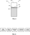
- one or more of the processes described here can be used to position the discrete component 10 on the device substrate 12 such that the active face 102 of the discrete component 10 is oriented toward the device substrate 12 (which we sometimes call a "face-down" position or a "flip-chip” configuration).
- the discrete component can be electrically connected to other components on the device substrate using flip-chip assembly methods such as conductive adhesives or soldering.
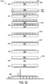
- Wafer processing (202) includes fabricating or obtaining wafers bearing large numbers of discrete components fabricated thereon. We sometimes refer to wafer processing as discrete component fabrication. The discrete components are fabricated on the wafers using semiconductor processing techniques such as thin film processing methods on a semiconductor substrate, such as a bulk silicon substrate, a silicon-on-insulator substrate, a germanium substrate, a gallium arsenide substrate, a sapphire substrate, or another type of semiconductor substrate.
- a semiconductor substrate such as a bulk silicon substrate, a silicon-on-insulator substrate, a germanium substrate, a gallium arsenide substrate, a sapphire substrate, or another type of semiconductor substrate.
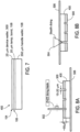
- Each of the general process steps shown in Fig. 5 can have one or more aspects, one or more of which can be carried out for each specific process described here.
- wafer thinning to a thickness of about 50 ⁇ m can be accomplished by mechanical backside grinding followed by polishing.
- the wafer is temporarily bonded to a support substrate 302, such as a thicker wafer (e.g., the 3M Wafer Support System ® ).
- a support substrate 302 such as a thicker wafer (e.g., the 3M Wafer Support System ® ).
- an active layer 310 on the top surface of the wafer 300, on which the integrated circuitry is formed faces down toward the support substrate 302.
- the thinned wafer is removed from the support substrate 304.
- the second surface 106 includes a pressure-sensitive adhesive and the first surface 104 can include a UV-release material or a thermal-release material.
- exemplary release materials that are compatible with semiconductor materials are known, and selectable based on the desired adhesion characteristics.
- the handle release layer 105 is formed of a material that responds mechanically to an applied stimulus.
- the handle release layer undergoes a mechanical change in response to a stimulus.
- the handle release layer can lose adhesion as a result of a change in surface morphology caused by application of the stimulus.
- Example handle release layers can be formed of materials that transition from smooth and highly adhesive to rough and poorly adhesive responsive to heat, ultraviolet light, or another type of stimulus.
- the handle release layer undergoes a phase transition in response to a stimulus, losing adhesion as a result of a physical change in state. The transition can be from the solid to the liquid phase (melting) or from the solid to the gas phase (sublimation).
- attachment means between the discrete component 10 and the handle substrate 108 is generally described as an adhesive tape, other arrangements would be possible. For example, vacuum or electrostatic forces could be used to form this attachment temporarily.
- the attachment means and characteristics, such as bond strength can be selected such that the bond strength between the discrete component and the substrate is greater than the bond strength between the discrete component and the handle as the discrete component is bonded with the substrate.
- the handle release layer 105 it is desirable to arrange for the handle release layer 105 to be relatively thin, for example to have a thickness less than 20 ⁇ m, preferably less than 10 ⁇ m, and in some cases less than 5 ⁇ m.
- a thin handle release layer enables the use of certain advantageous chip dicing methods and improves chip quality after dicing and transfer to the substrate.
- the use of thicker handle release layers can contribute to die chipping or cracking during the dicing process.
- wafer preparation can include dicing the wafer handle assembly 400 into handle assemblies 500 (sometimes referred to as singulating the wafer), or dicing a wafer without handle substrate into discrete components.
- a wafer handle assembly is a wafer attached to a handle substrate.
- a handle assembly is an individual discrete component attached to a portion of a handle substrate.
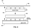
- the wafer handle assembly can be completely or partially diced by dry or wet etching, by plasma dicing, by mechanical sawing (as shown in Fig. 8A ), by laser ablation, by stealth dicing (as shown in Fig. 8B ), or by another dicing technique.
- the wafer handle assembly 400 is diced indirectly by laser micromachining (sometimes referred to as laser stealth dicing) using a laser beam 504 incident on the back side of the wafer handle assembly 400.
- laser micromachining sometimes referred to as laser stealth dicing
- mechanical sawing and laser stealth dicing are used sequentially to completely dice a wafer handle assembly 400.
- the wafer handle assembly 400 including the thinned wafer and the handle substrate can be diced.
- the thinned wafer is not attached to a handle substrate during dicing.
- the wafer handle assembly 400 or the wafer can be adhered to a dicing tape 506 for dicing.
- the dicing tape 506 can have a backing material of polyvinyl chloride (PVC), polyolefin, polyethylene, or another material, and an adhesive surface to which the wafer handle assembly or the wafer is adhered.
- wafer transfer can occur before wafer dicing.
- the wafer handle assembly or the wafer can be mounted on a transparent carrier and the mounted wafer handle assembly or wafer is diced.
- the transparent carrier can be formed of a material, such as glass or a transparent polymer, that is at least partially transparent to at least some wavelengths of the ultraviolet, visible, or infrared electromagnetic spectrum.
- the transparent carrier can have a layer of a dynamic releasing layer (DRL) disposed on a surface thereof, such as described in PCT WO2012/033147 .
- DRL dynamic releasing layer
- the wafer can be partially diced before the wafer transfer process step and dicing can be completed after the wafer transfer process step (described below).
- partially or completely diced handle assemblies or an undiced wafer or wafer handle assembly is transferred from a dicing tape to a transparent carrier or to a die carrier, such as a waffle pack, a gel pack, or another type of carrier.
- a die carrier such as a waffle pack, a gel pack, or another type of carrier.
- Various approaches can be used for wafer transfer, sometimes in combination with dicing processes.
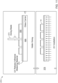
- diced handle assemblies 500 or discrete components are transferred from dicing tape 506 onto the transparent carrier 600 or a die carrier.
- the diced handle assemblies 500 or discrete components are removed from the dicing tape 506, for instance, using suction provided by a vacuum chuck 602.
- a transparent carrier 600 or a die carrier is brought into contact with the diced handle assemblies 500 or undiced wafer or wafer handle assembly that is suctioned onto the vacuum check 602.
- the suction force is removed, causing the handle assemblies 500 or undiced wafer or wafer handle assembly to be transferred onto the transparent carrier 600 or the die carrier.
- diced handle assemblies 500 or discrete components are transferred from dicing tape 506 onto the transparent carrier 600 or a die carrier.
- a wafer or wafer handle assembly is adhered to a dicing tape and diced into handle assemblies 500 or discrete components.
- the dicing tape 506 is formed of a material that undergoes a reduction in adhesion responsive to a stimulus, such as heat or light.
- the dicing tape 506 can be an ultraviolet (UV)-release adhesive that undergoes a reduction in adhesion when exposed to UV light.
- UV dicing tape is exposed to ultraviolet light 508, causing the adhesion between the diced handle assemblies or discrete components to be weakened.
- a vacuum chuck 510 is coated with a material 512 that undergoes a reduction in adhesion responsive to a stimulus, such as heat or light.
- the vacuum chuck 510 can be coated with a thermal release tape 512 (e.g., such as a REVALPHA ® double-coated thermal release tape by Nitto ® ) and a vacuum is drawn to keep the thermal release tape 512 in position.
- the diced handle assemblies 500 or discrete components are removed from the UV dicing tape 506 by contact with the tape-covered vacuum chuck 510.
- the thermal release tape 512 adheres to the diced handle assemblies 500 or discrete components with an adhesion that is greater than the weakened adhesion between the previously exposed UV dicing tape 506 and the diced handle assemblies 500 or discrete components, thus removing the diced handle assemblies 500 or discrete components from the dicing tape 506.
- the dicing tape 506 is peeled off, leaving the handle assemblies 500 or discrete components adhered to the thermal release tape 512.
- a transparent carrier 600 with a dynamic releasing layer disposed thereon is brought into contact with the diced handle assemblies 500 or discrete components adhered to the thermal release tape 512 on the vacuum chuck 510.
- the transparent carrier 600 can be placed on top of the diced handle assemblies 500 or discrete components and weighted for strong contact.
- a positive pressure can be applied to the vacuum chuck 510 to push the thermal release tape 512 away from the chuck 510, thus further pressing the diced handle assemblies or discrete components against the dynamic releasing layer of the transparent carrier 600.
- the stack including the transparent carrier 600, diced handle assemblies 500 or discrete components, and the thermal release tape 512 is removed from the vacuum chuck 510 and heated to a temperature at which the thermal release tape loses some or all of its adhesion (referred to as the characteristic temperature of the thermal release tape).
- the thermal release tape 512 is then peeled off, leaving the diced handle assemblies 500 or discrete components on the transparent carrier 600.
- the wafer transfer approach 320 can be used as long as the characteristic temperature of the thermal release tape is lower than the temperature that causes the handle release layer 105 of the handle assemblies to melt, flow, or degrade. Losses can also be mitigated by providing uniform contact between the discrete components or handle assemblies and the dynamic releasing layer on the transparent carrier, e.g., by providing a flat vacuum chuck and flat surface of the dynamic releasing layer or by providing positive pressure from the vacuum chuck to force a better contact. In some cases, accuracy of placement of discrete components or handle assembles on the transparent carrier can be facilitated by lifting the thermal release tape straight up when removing the thermal release tape.
- a wafer 300 or wafer handle assembly is adhered to the transparent carrier 600 via a material with controllable adhesion 374.
- the material with controllable adhesion 374 includes both the dynamic releasing layer and a UV or thermal release adhesive.
- the wafer 300 or wafer handle assembly is diced (372) directly on the transparent carrier 600.
- the material with controllable adhesion 374 has an adhesion that is strong enough to allow for secure attachment of the wafer 300 or wafer handle assembly to the transparent carrier 600 during dicing.
- the material with controllable adhesion 374 is exposed to a stimulus (376), such as heat or ultraviolet light, causing the adhesion of the material 374 to be reduced.
- a stimulus such as heat or ultraviolet light
- the adhesion level of the material 374 following exposure can be controlled by controlling parameters of the stimulus, such as the exposure intensity (e.g., the intensity of the ultraviolet light or the temperature), exposure time, or other stimulus parameters.
- the adhesion of the material 374 can be reduced to a level compatible with the laser assisted contactless transfer method 800 described below.
- the wafer transfer approach 350 eliminates the component transfer process (discussed below), thus simplifying the process flow. In addition, without a component transfer process, there is no possibility of loss of discrete components or handle assemblies during component transfer, and thus process yield can be improved using the wafer transfer approach 350.
- a wafer or wafer handle assembly 400 is partially diced (552), e.g., using partial blade dicing (as shown), laser dicing, wet etching, or another approach. Partial dicing removes the passivation layer and the metal from the spaces (sometimes called streets) between the discrete components on the wafer or wafer handle assembly 400, leaving a small amount of material (e.g., less than about 20 ⁇ m, such as about 5 ⁇ m, about 10 ⁇ m, about 15 ⁇ m, about 20 ⁇ m, or another amount) at the bottom of each dicing street. Partial dicing facilitates subsequent non-contact dicing such as plasma dicing.
- a wafer transfer approach 570 the wafer or wafer handle assembly 400 is completely diced on dicing tape.
- a two-step dicing process can be used in which the wafer or wafer handle assembly 400 is partially diced with a dicing blade (572) followed by complete dicing using a stealth dicing approach (574).
- the diced discrete components or handle assemblies are transferred (576) to a vacuum chuck covered with a thermal release tape (e.g., Revalpha) and released to a transparent carrier 600 (578) as described above for the wafer transfer approach 320.
- a thermal release tape e.g., Revalpha
- the transparent carrier includes a material with controllable adhesion 580, in addition to or in place of the dynamic releasing layer. Once the diced discrete components are adhered to the transparent carrier, the material with controllable adhesion 580 is exposed to a stimulus (582) as described above for the wafer transfer approach 370 to reduce the adhesion of the material 580 to a level compatible with the laser assisted contactless transfer method 800 described below.
- the wafer transfer approach 570 can achieve lower loss of discrete components or handle assemblies and can enable precise control of the laser assisted contactless transfer method 800 via control of the adhesion level of the material 580.
- pick-and-place tools are used to transfer handle assemblies or discrete components to the transparent carrier.
- the handle assemblies or discrete components can be rearranged on the transparent carrier according to a desired placement, e.g., in a rectangular array, enabling simplification of placement algorithms.
- This approach also allows only "good" handle assemblies or discrete components to be transferred, thus improving downstream yield.
- This wafer transfer approach may be limited to handle assemblies or discrete components having sizes compatible with pick-and-place equipment and can sometimes have low throughput compared to other wafer transfer approaches.
- This wafer transfer approach can be useful in prototyping, e.g., in processes in which individual discrete components are thinned and prepared for laser transfer.
- Some processes described here do not include the wafer transfer process step. For instance, processes in which the wafer is mounted on a transparent carrier prior to dicing do not include the wafer transfer process step.
- the device substrate or the discrete components or both can be provided with an attachment element that promotes attachment, such as adhesion, electrical connection, or both, between the discrete components and the device substrate.
- the attachment element can be a material that is curable responsive to an applied stimulus, such as a material that is thermally curable, curable upon exposure to ultraviolet (UV) light, curable upon exposure to mechanical pressure, or otherwise curable.
- the attachment element can be a conductive material, such as a conductive epoxy, e.g., a conductive paste including metal (e.g., silver) or metal-coated particles in a paste, a solder paste, or another conductive material.
- the attachment element can be a non-conductive material, such as Ablebond 8008NC (Henkel Electronic Materials, Irvine, CA).
- the attachment element can be a film, such as an anisotropic conductive film or a non-conductive die attach film.
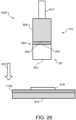
- the pick-and-place approach 700 includes a tool 702 that transfers a handle assembly 500 onto a device substrate 704.
- the tool 702 picks up the handle assembly 500, e.g., by applying a suction to the handle substrate 108 of the handle assembly 500.
- the tool 702 positions the handle assembly 500 directly over an attachment surface 708 on the device substrate 704.
- the tool 702 then moves the handle assembly 500 toward the device substrate 704, for example, in a direction generally show by an arrow 710, until the discrete component 10 contacts the attachment surface 708 on the device substrate 704.
- a laser assisted contactless transfer method 800 which we sometimes call tmSLADT (thermo-mechanical selective laser assisted die transfer).
- the handle assemblies 500 (as shown) or discrete components are adhered to a transparent carrier 600 having a dynamic releasing layer (DRL) 604 disposed thereon, as described above, by an adhesive layer 802.
- the combination of DRL 604 and adhesive layer 802 is sometimes referred to as a carrier release layer.
- the dynamic releasing layer (DRL) 604 is illuminated with light 804 from a laser.
- the DRL 604 absorbs the energy incident thereon from the laser light 804, heating up and partially evaporating, and resulting in formation of a blister 806.
- the blister 806 mechanically pushes the handle assembly 500 onto the attachment surface 708 of the device substrate 704.
- the tmSLADT method is described in PCT WO2012/142177 .
- the adhesion of the adhesive layer 802 is an important parameter in the tmSLADT process 800.
- Fb the force of the expanding blister
- Fa the force of the expanding blister
- the adhesive force between the discrete component or handle assembly and the DRL 604 can be kept at a low level, e.g., just enough to prevent the gravitational force from making the discrete component or handle assembly drop.
- a larger adhesive force to the DRL 604 can be helpful.
- the transfer thus involves a balance between the adhesive forces of the dicing tape and the DRL 604 and the suction force of the transfer device (e.g., the vacuum chuck).
- the wafer transfer approaches described above are operable with various levels of adhesion to the DRL 604, providing flexibility for successful tmSLADT transfer.
- component transfer can include both tmSLADT and pick-and-place approaches.
- discrete components can be transferred to a handle substrate via a tmSLADT approach to form handle assemblies, which can be transferred to the device substrate by a pick-and-place approach.
- handle assemblies can be transferred to a transparent carrier using a pick-and-place approach and then transferred to the device substrate via a tmSLADT approach.
- Discrete components can be transferred onto the device substrate in a face up orientation such that the active face of the discrete components faces up (such as shown in Fig. 1A ), e.g., for wire bonding applications.
- Discrete components can be transferred onto the device substrate in a face down orientation such that the active face of the discrete components faces down (such as shown in Fig. 1B ), e.g., for flip chip assembly.
- a bonding tool applies a stimulus to the attachment element, such as a high temperature, ultraviolet light, mechanical pressure, or another stimulus, or a combination of any two or more of them.
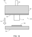
- the bonding tool can apply the stimulus through the discrete component (as shown in Fig. 14 ), through the device substrate, or both.
- the bonding tool is the same tool as the tool that transfers a handle assembly onto the device substrate in the pick-and-place approach to component transfer. The stimulus is removed after a time sufficient to allow the attachment element to cure, forming a mechanical bond, an electrical bond, or both between the discrete components and the device substrate.
- the component interconnection process step can include wire bonding. In some examples, the component interconnection process step can include placing the discrete components onto the device substrate in a face-up configuration and printing a conductive material onto the substrate and the active face of the discrete components.
- the handle substrate is detached from the discrete component and removed, leaving only the discrete component bonded to the device substrate.
- the handle substrate is attached to the discrete component via a handle release layer, which provides adhesion between the discrete component and the handle substrate that can be released responsive to an applied stimulus, such as temperature, ultraviolet light, a normal or shear mechanical force, or another type of stimulus, or a combination of any two or more of them.
- a release tool applies a stimulus to the handle release layer, such as high temperature, ultraviolet light, normal or shear force, or another stimulus, or a combination of any two or more of them.
- the release tool can apply the stimulus through the discrete component, through the device substrate, or both.
- the release tool is the same as the bonding tool that applies a stimulus to the attachment element.
- the stimulus is removed after a time sufficient to allow release of the handle release layer.
- the handle substrate is removed, e.g., by a suction force, by forced air, by an action of the release tool, or in another way.
- a handle substrate is not used, and thus the handle removal process step is not carried out.
- Handle Removal Handle assisted packaging (900) Wafer thinning; To die carrier (optional) Pick-and-place Curing of attachment element Handle detachment and removal Handle attachment; Dicing on dicing tape Laser enabled packaging (150) Wafer thinning; To transparent carrier Laser assisted contactless transfer Curing of attachment element N/A Dicing on dicing tape Direct laser enabled packaging (160) Wafer thinning; N/A Laser assisted contactless transfer Curing of attachment element N/A Dicing on transparent carrier Laser enabled, handle assisted packaging (180) Wafer thinning; To transparent carrier Laser assisted contactless transfer Curing of attachment element Handle detachment and removal Handle attachment; Dicing on dicing tape Direct laser enabled, handle assisted packaging (250) Wafer thinning; N/A Laser assisted contactless transfer Curing of attachment element Handle detachment and removal Handle attachment; Dicing on transparent carrier Handle assisted ultra-small chip assembly (350, 380) Wafer thinning; N/A Laser assisted contactless transfer onto handle; Curing of attachment
- a process 410 for packaging ultra-small and ultra-thin discrete components can generally include discrete component fabrication (412), wafer preparation (414-422), discrete component transfer (424-430), , discrete component interconnection (430), and handle removal.
- Discrete component transfer in the process 410 includes discrete component transfer onto a handle substrate (424), handle substrate dicing (416426 attachment site preparation (428), and discrete component transfer onto the device substrate (430).
- wafers bearing large numbers of discrete components can be fabricated using known semiconductor techniques such as thin-film methods on a semiconductor material, for example, on a bulk silicon substrates or on layered silicon-insulator-silicon substrates (412).
- Wafer preparation in the process 410 can include partial dicing (404) of the wafer using known semiconductor techniques.
- the discrete components can be partially separated by dry or wet etching, by mechanical sawing (as shown in Fig. 16 ), or by laser micromachining.
- the wafer surface can be protected from damage with a masking film and/or a passivation layer.
- a layer of photoresist, polymers, UV-curable polyimide, laminating films, or another suitable material can be applied and patterned using methods of photolithography or stencil/screen printing.
- the wafer can be thinned to a thickness of approximately 50 ⁇ m using a mechanical grinding technique such as backgrinding.
- a mechanical grinding technique such as backgrinding.
- a noncontact material removal process can be used to reduce the wafer thickness beyond what is achievable by the conventional mechanical grinding process.
- a known noncontact material removal process such as Reactive Ion Etching (RIE), vapor phase etching, or any other appropriate processes can be used to produce the thin wafer.
- the discrete components are formed by the separation of portions of the semiconductor material from the wafer, for example, along the streets formed in the wafer. As shown in Fig. 16 , individual discrete components can be released from the wafer using a dry etching technique, for example, RIE is used (420-422). As described above, the parameters and plasma gas composition are selected such that the silicon in the streets is completely etched or removed (420) prior to etching or removing any other mask material (422). For example, a photoresist material and thickness can be selected, depending on the process parameters and plasma gas compositions if a RIE is used.
- RIE reactive etching
- the parameters and plasma gas composition are selected such that the silicon in the streets is completely etched or removed prior to etching or removing any other mask material.
- process parameters include a 1:1 mix of SF6 and O2 as a plasma gas, pressure 13-14 Pa, power 135 W, and DC-bias 150 V.
- etching continues until the masking layer is completely removed from the discrete component surface.
- Component transfer in the process 410 which includes releasing the individual discrete components from the handling substrate, will depend upon the handling substrate material and/or adhesive material used.
- the discrete components for example, are mounted to a glass interim handle using a DRL layer.
- the discrete components can be released from the DRL using a laser transfer method (424) without contacting the ultra-thin discrete component.
- Other methods than can handle ultra-thin discrete components can be used to transfer the discrete components to the handle substrate.
- component transfer includes both a laser transfer method and pick-and-place.
- the discrete components are transferred from the DRL onto a handle substrate using a laser transfer method.
- the handle substrate provides a larger handle that is compatible in size with a pick-and-place approach to component transfer, thus enabling the handle assemblies to be transferred to the device substrate by a pick-and-place approach.
- the discrete components can be released from the DRL layer and attached to a handle substrate by using a laser contactless technology (424) for ultra-thin chips assembly (which we call tmSLADT), disclosed in PCT WO2012142177 .
- a distance 508 between each discrete component 10 is selectable based on the capabilities of the wafer dicing tool, for example, kerf and precision, dimensions of the ultra-small and ultra-thin discrete component 10, and dimensions of the handle 108.
- Suitable wafer dicing tools and/or methods include sawing, laser cutting, scribing, stealth dicing, and other known suitable methods.
- the distance 502 is greater than 50 ⁇ m, for example, inclusive of and between 50 ⁇ m and 200 ⁇ m.
- the handle assembly 100 Prior to forming the individual handle assemblies, for example, the handle assembly 100, one or more discrete components 10 are released onto an oversized handle substrate 108a to form an oversized handle assembly 510.
- the oversized handle assembly is positioned below the glass interim handle from which the discrete components are released using the laser transfer method so that when the discrete components are released from the glass interim handle, each discrete component travels in a direction generally indicated by arrow 512 towards a handle release layer 105a, which is pre-coated, for example, using any suitable process such as lamination or spin coating, onto the handle substrate 108a.
- the properties of the handle substrate 108a, the handle release layer 105a including a second surface 106a and a first surface 104a are generally similar to those described with reference to the handle assembly 100, with the exception of the increased size of the handle substrate 108a and associated handle release layer 105a.
- the second surface 106a includes a pressure activated adhesive for attachment of the handle release layer 105a to the handle substrate 108a and the first surface 104a includes a thermal-release surface or a UV release surface, for example, a thermal-release layer or a UV-release layer for attaching the discrete component 10 to the handle release layer 105a.
- the discrete component comes into contact with the handle release layer 105a, the discrete component is releasably attached to the handle substrate 108a, until, for example, an application of heat or UV light.
- the handle release layer 105a is a single layer such that the first surface 104a and the second surface 106a are the same material, for example, a thermal release adhesive or a UV-release adhesive.
- Component transfer in the process 410 includes transferring the handle assemblies 100 onto the device substrate.
- the methods described herein are used to attach ultra-thin and/or ultra-small bare discrete components to any device substrate used in integrated circuit packaging, such as a printed circuit board, plastic casing, ceramic substrate, flexible circuit, or other device substrates.
- attachment means for the discrete component can be provided prior to attaching the discrete components to a device substrate, for example a device substrate 614.
- a thermally cured non-conductive discrete component attachment material such as Ablebond 8008NC by Henkel
- a transfer 610 to a device substrate can include, for example, a discrete component bonding tool 612, a handle assembly 100, and a device substrate 614.
- the discrete component bonding tool 612 attaches to the handle substrate 108 of the handle substrate assembly 100.
- the discrete component bonding tool 612 moves towards the device substrate and positions the discrete component 10 directly over the attachment surface 618 on the device substrate 614.
- the discrete component bonding tool 612 then moves the handle assembly 100 toward the device substrate, for example, in a direction generally show by an arrow 620, until the discrete component 10 contacts the adhesive surface 618. Once contact is made, discrete component interconnection and handle removal are performed.
- the discrete component bonding tool applies a force and temperature profile that can cure the adhesive on the adhesive surface 618. Because the discrete component 10 is attached to the handle substrate assembly through a thermal-release layer, temperature profile delivered to the adhesive on the adhesive surface 618 quickly or simultaneously weakens the adhesion between the discrete components 10 from the handle substrate 108. Any remaining bond strength between the handle substrate 108 and the discrete component 10 is insufficient to overcome the bond strength between the discrete component 10 and the device substrate 614. As a result, the discrete component 10 remains attached to the device surface as the discrete component bonding tool 612 and handle substrate move away from the device substrate. The handle substrate can subsequently be released from the discrete component bonding tool for disposal at a different location by applying a positive pressure through the discrete component bonding tool.
- the transfer means for example, the discrete component bonding tool 612
- the transfer means can be facilitated with a device that is capable of emitting UV light.
- the UV-release discrete component bonding tool can emit UV light with sufficient intensity to de-bond the discrete component from the handle.
- an additional heat source is required to bond the discrete component to the device substrate.
- Such a heat source can be integrated with the work table that holds the device substrate.
- the discrete component can be bonded to the handle substrate by a UV releasable layer while the adhesive on the device substrate can be a UV-cured adhesive material.
- emitting a UV light of a sufficient intensity can weaken the bond between the discrete component and the handle substrate and bond the discrete component to the adhesive on the device substrate.
- thermally sensitive or UV sensitive adhesives are used such that the bond between the discrete component and the handle substrate weakens while the bond between the discrete component and the device substrate strengthens.
- heat or UV light are also or alternatively applied through the device substrate to cure the adhesive on the device substrate.
- transferring the discrete component to a device substrate can include the steps as follows.
- a process 720 for packaging ultra-small and/or ultra-thin discrete components in a face up configuration can generally include obtaining or fabricating a wafer (722), partially dicing the wafer (724), thinning the wafer (726), separating the discrete components from the wafer (728), transfer the discrete components from the wafer to an interim handle substrate (730), transfer the discrete components from the interim handle substrate to the handle substrate (732), bonding the discrete components to the handle substrate while weakening the bond between the interim handle substrate and the discrete components (732), dividing the handle substrate into a plurality of individual handle substrates each including a discrete component (734), preparing the device substrate for attachment with the discrete component (736), picking up the handle assembly using a discrete component bonding tool and positioning the handle assembly over the device substrate to align the discrete component with the attachment adhesive on the device substrate (738), moving the discrete component into contact with the attachment adhesive on the device substrate (738), emitting energy such that the bond between the discrete component
- wafers bearing large numbers of discrete components can be fabricated using known semiconductor techniques such as thin-film methods on a semiconductor material, for example, on bulk silicon substrates or on layered silicon-insulator-silicon substrates (722).
- the wafers can undergo partial dicing using known semiconductor techniques.
- the discrete components can be partially separated by dry or wet etching, by mechanical sawing (as shown in Fig. 19 ), or by laser cutting.
- the wafer is diced to form street depth equal or slightly greater than the final discrete component thickness.
- wafer thinning, discrete component separation are generally similar to the wafer thinning, and discrete component separation described with reference to the process 410 except for any discussion related to a masking film.
- the process 720 omits a masking film so the dry etching (728) is simply carried out until the streets are unobstructed.
- an oversized handle assembly 810 is generally similar to the oversized handle assembly 510, with the exception of the location of the active discrete component face 102 and the type of handle release layer 815.
- the active discrete component face is oriented away from the interim substrate 818.
- the interim substrate 818 is coated with a low-temperature adhesive heat-release tape so that when the tape is exposed to a certain temperature, the tape loses its adhesive properties.
- REVALPHA 319Y-4L by Nitto ® has a release temperature of 90 °C.
- the interim handle substrate 818 is placed over or stacked on the handle substrate 108.
- the handle substrate 108 includes handle release layer 105 including a layer 104 that heat sensitive with a higher release temperature, for example, REVALPHA 319Y-4H by Nitto ® with a release temperature of 150 °C, than the release temperature of the interim handle substrate.
- the stack is heated to a temperature higher than the release temperature of the low-temperature tape but lower than the release temperature of the high-temperature tape. The conditions result in the interim handle substrate 818 losing adhesion.
- the interim handle substrate is freely removable. In some cases, the interim substrate assembly is also reusable.
- heating is a mode of causing the interim handle substrate to lose adhesion
- a variety of techniques can be used for that purpose.
- the handle release layer could be made to lose adhesion by applying a stimulus to cause a change in the surface morphology of the handle release layer.
- the stimulus could be heat or UV light and the corresponding change in the surface morphology of the handle release layer could include formation of small blisters on the surface.
- Such a change in the surface morphology from smooth to blistered will cause a transition of adhesion from sufficiently adhesive to very rough with very low adhesion.
- the material used for the handle release layer can be chosen to respond to such a stimulus by changing its surface morphology.
- the reduction in adhesion is achieved by a phase transition in which the handle release layer loses adhesion by a physical change of state caused by applying a stimulus.
- the phase transition can be from a solid phase to a liquid phase (for example, melting) or from a solid phase to a gas phase (sublimation) or a combination of them.
- the stimulus could be light, heat, pressure, or a combination of any two or more of them.
- the loss of adhesion could be caused by a chemical process.
- chemically triggered loss of adhesion could be based on a change in the chemical structure or composition of the handle release layer or components of it.
- the handle release layer or components of it can be ones that change their chemical structure when exposed to the stimulus.
- the materials can be ones that change their chemical composition (e.g., degrade) when the stimulus is applied.
- Such materials could include: i) materials that undergo thermal decomposition, or thermolysis, which is a chemical decomposition caused by heat, and ii) materials that undergo photodegradation, which is degradation caused by the absorption of light.
- the stimulus for the chemical process could be light or heat or both.
- the release mechanism does not involve melting of the handle release layer material. Release without melting of the handle layer allows the handle substrate to be removed by a vertical motion rather than a lateral sliding motion.
- Vertical removal of the handle substrate can be advantageous, e.g., when the handle substrate is removed by a conventional die bonder. Removal of the handle substrate by a lateral sliding motion can be advantageous in environments such as roll-to-roll assembly lines in which the handle substrate forms part of a continuous web. Release without melting of the handle release layer material can help avoid leaving a residue on the surface of the discrete component after handle removal.
- the handle release layer or the process of reducing its adhesion or both can be selected so that the loss of adhesion is permanent or so that the restoration of adhesion is prevented, inhibited, or delayed.
- This approach has the advantage of reducing or eliminating a time constraint on when the handle must be removed. For instance, such materials may undergo a restoration of adhesion within about 10 seconds, 30 seconds, one minute, 5 minutes, 10 minutes, or another time following reduction of adhesion. Melting a wax, for example, to reduce the adhesion of the handle release layer will leave very little time for removing the handle after the heat that causes the melting of the wax is reduced, because the wax will re-solidify relatively quickly.
- Example materials in which the loss of adhesion is permanent or the restoration of adhesion is prevented, inhibited, or delayed include materials that degrade, decompose, or sublimate; or adhesive tapes such as REVALPHA ® double-coated thermal release tape by Nitto ® .
- the material of the handle release layer or the process of releasing it or both can be selected so that no residue remains on the discrete component after the release.
- materials that leave no residue on the discrete component after the release can include materials that change surface morphology (e.g., such as a REVALPHA ® double-coated thermal release tape by Nitto ® ) or materials that sublimate.
- the discrete component packaging process including preparing the device substrate (736) and transferring the discrete component to the device substrate (738) is generally similar to the discrete component packaging process described with respect to Fig. 16 .
- a process 1000 for packaging ultra-small and ultra-thin discrete components in a flip-chip configuration can generally include obtaining or fabricating a wafer (1002), partially dicing the wafer (1004), thinning the wafer (1006), separating the discrete components from the wafer (1008), transfer the discrete components to a handle substrate (1010) dividing the handle substrate into a plurality of individual handle substrates each including a discrete component (1012), preparing the device substrate for attachment with the discrete component (1014), picking up the handle assembly using a discrete component bonding tool and positioning the handle assembly over the device substrate to align the discrete component with the attachment adhesive on the device substrate (1016), moving the discrete component into contact with the attachment adhesive on the device substrate (1016), emitting energy such that the bond between the discrete component and the handle substrate weakens while the bond between the discrete component and the device substrate strengthens, (1016) moving the discrete component bonding tool away from the device substrate while the discrete component remains bonded to the device substrate, and
- wafers having bumped out discrete components are generally known.
- Common methods for wafer bumping include stud bumping, electroless nickel-gold plating, solder balls, solder paste printing, solder electroplating, etc. While an initial wafer having a low profile electroless nickel-gold plating is compatible with the process described here, the creation of bumps can occur after transferring the discrete components from the glass substrate (1010) and before placing the discrete components on the handle substrate (1012).
- the wafer dicing process (1004), the wafer thinning process (1006), the discrete component separation (1008), the discrete component transfer (1010), forming individual handle substrates (1012), and discrete component bonding (1016) are generally similar to other methods discussed above.
- the discrete components 10 are placed on the handle substrate 108, as shown in Figs. 17 and 23 , in the same manner but for the orientation of the active face 102 on the discrete component 10.
- each of the discrete components 10 are separated by a distance 1202 and travel along a direction 1204.
- the discrete component bonding generally includes picking up the handle assembly using a discrete component bonding tool and positioning the handle assembly over the device substrate to align the discrete component with the attachment adhesive on the device substrate (1016), moving the discrete component into contact with the attachment adhesive on the device substrate (1016), emitting energy such that the bond between the discrete component and the handle substrate weakens while the bond between the discrete component and the device substrate strengthens, (1016) moving the discrete component bonding tool away from the device substrate while the discrete component remains bonded to the device substrate, and releasing the handle substrate from the discrete component bonding tool (1016).
- Wafer preparation in the process 1300 includes wafer thinning, handle attachment, and dicing.
- the wafer is thinned, e.g., to a thickness of less than 50 ⁇ m, such as a thickness of about 25 ⁇ m.
- the wafer can be thinned using a mechanical thinning process or a mechanical thinning process followed by a non-contact thinning process (1304).
- the ultra-thin wafer is mounted to a handle substrate (1306).
- the back side of the wafer is bonded to a 350 ⁇ m thick handle substrate via a 20 ⁇ m thick handle release layer, leaving the active layer of the wafer exposed.
- the active layer of the wafer can be bonded to the handle substrate, leaving the back side of the wafer exposed.
- the process 150 can have advantages. For instance, the use of the laser assisted contactless transfer method to perform component transfer allows the process to be applied to the transfer of a wide range of sizes and types of components, such as components that are too small for a pick-and-place approach or components that are unsuited to be mounted on a handle substrate.
- the process 150 can operate with a higher throughput than other processes that are not laser assisted, because the laser can be electronically scanned to rapidly transfer successive discrete components with little or no realignment of the transparent carrier.
- a laser enabled packaging process (160) enables packaging of ultra-small discrete components without use of a handle substrate.
- a wafer bearing large numbers of discrete components is fabricated or obtained (162).
- discrete component interconnection is performed while the discrete components are still attached to the associated portion of the handle substrate.
- the thick assembly of a discrete component and a handle substrate is less prone to cracking during curing of the attachment element on the device substrate (e.g., during curing of a conductive epoxy) during discrete component interconnection than is a discrete component that is not mounted on a handle substrate.
- a laser enabled, handle assisted packaging process 250 enables packaging of ultra-thin discrete component.
- a wafer bearing large numbers of discrete components is fabricated or obtained (252).
- the back side of the wafer is bonded to a 350 ⁇ m thick handle substrate via a 20 ⁇ m thick handle release layer, leaving the active layer of the wafer exposed.
- the active layer of the wafer can be bonded to the handle substrate, leaving the back side of the wafer exposed.
- Component transfer in process 250 includes releasing the discrete components from the transparent carrier (264) using the laser assisted contactless transfer method described above.
- the discrete components are transferred onto a device substrate having attachment element formed thereon.
- Discrete component interconnection (266) and handle removal (268) are performed by applying pressure, temperature, or ultraviolet light as described above.
- the use of the laser assisted contactless transfer method to perform component transfer allows the process to be applied to the transfer of a wide range of sizes and types of components, such as components that are too thin for a pick-and-place approach.
- the process 250 can have advantages. For instance, the process 250 has a simplified process flow relative to other laser assisted processes by the elimination of the diced wafer transfer step.
- the process yield can be improved because there is no opportunity for die loss during transfer of diced discrete components.
- the possibility of die shifting or rotating with respect to their original positions in the wafer during transfer of the diced discrete components is eliminated because the wafer is transferred as an intact unit.
- the process 1500 can then generally include picking up (1502) the handle assembly 1552 (which includes the discrete component 1501, the handle substrate 108, the handle release layer 105) by applying a vacuum 1513 through a vacuum tube 1516 of a discrete component transfer tool 1508.
- the transfer tool with the handle assemble is then positioned (1502) over the location 1515 of the device substrate as also shown in Figs. 25 and 26 , aligning the discrete component with the attachment adhesive on the device substrate 1502 (614 in Fig. 18 ).
- the discrete component is then moved into contact with the attachment adhesive 1505 (618 in Fig. 18 ) on the device substrate 1502.
- the vacuum in the vacuum tube can be broken to release the transfer tool 1508 from the handle and the transfer tool can be moved away. Then a separate discrete component bonding tool 1510 may be moved into contact with the discrete component.
- Pressure 1550 or energy 1551 e.g., thermal or UV energy, or both
- Pressure 1550 or energy 1551 then can be applied 1517 to the discrete component 1501, the handle substrate 108, the handle release layer 105 through a contact surface 1519 of the bonding tool 1510 into the handle and also through the handle to the bond 1521, through the bond to the discrete component 1501, and through the discrete component 1501 to the bond 1523 with the device substrate.
- the pressure or energy or both can simultaneously or in sequence cause the bond 1521 between the discrete component and the handle substrate to weaken and the bond 1523 between the discrete component and the device substrate to strengthen (1504).
- the pressure can operate simultaneously to weaken the bond 1521 and to strengthen the bond 1523.
- energy in some cases, the energy must flow through the successive elements of the system so that the weakening of bond 1521 may begin or be completed before the strengthening of the bond 1523 begins or is completed, or the weakening and the strengthening can occur in sequence.
- the handle release layer 105 and the attachment adhesive are selected such that the bond 1523 between the discrete component 1501 and the device substrate 1502 forms before the bond 1521 is formed between the handle and the discrete component 1501, or the formation of the bond 1523 and the bond 1521 can occur simultaneously with complete overlap in time, or the formation can overlap partly with either the bond 1523 or the bond 1521 partly occurring earlier than or later than the overlapping period.
- the formation of either the bond 1523 or the bond 1521 can include a hardening or softening of a material, e.g., a wax material.
- the handle release layer 105, the attachment adhesive 1505, or both the handle release layer 105 and the attachment adhesive 1505 may include one or more materials that soften or harden in response to an application of energy.
- the softening of the bond 1523 can occur before the hardening of the bond 1521, or the softening of the bond 1523 can occur after the hardening of the bond 1521, or the two events can occur simultaneously with complete overlap in time, or they can overlap but one or the other can partly occur earlier than or later than the overlapping period.
- the discrete component bonding tool 1510 may be removed leaving the handle assembly (including the discrete component 1501, the handle substrate 108, the handle release layer 105) in contact with the discrete component, which is bonded to the device substrate 1502. While not bonded to the discrete component (because of the weakening of bond 1523), the handle remains in contact with the discrete component, for example, due to gravitational force, surface attraction force, or residual adhesive force remaining after the debonding process, or a combination of two or more of these forces the two.
- the handle substrate may then be removed (1506) from the discrete component using any of a variety of separation techniques, e.g., brushing, compressed air, vacuum, vibration, liquid jet, electrostatic, electromagnetic force reorienting the device substrate such that gravity separates the handle from the discrete component, or any combination of two or more of those.
- separation techniques e.g., brushing, compressed air, vacuum, vibration, liquid jet, electrostatic, electromagnetic force reorienting the device substrate such that gravity separates the handle from the discrete component, or any combination of two or more of those.
- separation techniques e.g., brushing, compressed air, vacuum, vibration, liquid jet, electrostatic, electromagnetic force reorienting the device substrate such that gravity separates the handle from the discrete component, or any combination of two or more of those.
- separation techniques e.g., techniques applying force, energy, contact, and any combination of two or more of these to separate the handle substrate from the discrete component so long as the discrete component and/or the handle substrate are not damaged.
- the discrete transfer tool 1508 may be configured to apply a vacuum force to the handle assembly similarly to the use of the discrete component transfer tool 612 in Fig. 18 . In some examples, the discrete transfer tool 1508 may be configured to apply pressure, heat, or UV light, or a combination of them to the handle assembly similarly to use of the discrete component transfer tool 602 in Fig. 18 .
- Fig. 31 shows the removal of one handle assembly; the same separation technique or techniques may be used to remove two or more handle assemblies at the same time.
- multiple handle substrates may be arranged in proximity to each other such that a brush, a blade, an application of compressed air, an application of a vacuum, or an application of a vibrational force, or any combination of two or more of them, may remove the two or more handle assemblies from their corresponding discrete components.
- one or more of the processes described here can be used to position thin discrete components onto a device substrate starting from individual discrete components with regular thickness rather than starting from a wafer.
- Processes starting from individual discrete components can be used to place multiple, different discrete components on a single device substrate.
- the pick-and-place approach or the laser assisted contactless transfer method can be used to position individual discrete components in target positions in the device substrate.
- the device substrate can remain stationary and each discrete component can be moved relative to the device substrate until its target position is reached.
- the device substrate can be moved relative to the discrete components until the target position for a particular discrete component is positioned under that discrete component.
- the ability to place multiple, different discrete components onto a single substrate can have applications in research and development, for instance, in order to facilitate testing of multiple types of discrete components.
- individual discrete components 452 are received and mounted (440) on a first handle substrate 454 via a handle release layer 456.
- the discrete components 452 can be mounted onto the first handle substrate 454 by a pick-and-place approach or another method for positioning discrete components.
- the discrete components can be of various sizes and thicknesses that are compatible with a pick-and-place approach.
- a second handle substrate 456 having a handle release layer 458 and a layer of flowable material 460 disposed thereon is brought into contact (441) with the discrete components 452 on the first handle substrate 454.
- flowable material broadly to include, for example, any material that has a viscosity that enables the flowable material to flow responsive to a stimulus, such as pressure and vacuum lamination applied when the second handle substrate 456 is brought into contact with the discrete components 452 on the first handle substrate 454.
- Example flowable materials can include materials that undergo a phase change from liquid to solid responsive to application of a stimulus such as heat or light (e.g., ultraviolet light).
Landscapes
- Engineering & Computer Science (AREA)
- Mechanical Engineering (AREA)
- Container, Conveyance, Adherence, Positioning, Of Wafer (AREA)
- Dicing (AREA)
- Wire Bonding (AREA)
- Die Bonding (AREA)
- Physics & Mathematics (AREA)
- Plasma & Fusion (AREA)
- Fixed Capacitors And Capacitor Manufacturing Machines (AREA)
- Electron Tubes For Measurement (AREA)
- Packaging Of Annular Or Rod-Shaped Articles, Wearing Apparel, Cassettes, Or The Like (AREA)
Description
- Known assembly processes automate transferring items from one place to another using robotic pick-and-place systems, fluidic self-assembly systems, light-assisted assembly systems, or other systems.
-
US 2010/072490 A1 describes methods and systems for assembling electronic devices, such as integrated circuit (IC) chips, onto a subsequent flexible surface using a release member having a phase change material. Specifically, IC elements/components can be selectively received, stored, inspected, repaired, and/or released in a scalable manner during the assembly of IC chips by inducing phase change of the phase change material. The release member can be flexible or rigid. In some examples, the release member can be used with an intermediate transfer member. In some examples the IC element can be incorporated into a subsequent flexible surface including components for a TV, radiographic detector, sensor array, or any similar product having a requirement to emit, detect, or collect energy. In addition, the IC elements can be RF emitting, or visually emitting. -
US 2008/003780 A1 describes a technique to fabricate a package. A thin wafer supported by a wafer support substrate (WSS) is formed. The WSS-supported thin wafer is mounted onto a stiffener. The WSS is released from the thin wafer. The thin wafer and the stiffener are diced into a plurality of stiffener-reinforced dice. -
US 2014/004685 A1 describes a laser and plasma etch wafer dicing using UV-curable adhesive films. A mask is formed covering ICs formed on the wafer, as well as any bumps providing an interface to the ICs. The semiconductor wafer is coupled to a carrier substrate by a double-sided UV-curable adhesive film. The mask is patterned by laser scribing to provide a patterned mask with gaps. The patterning exposes regions of the semiconductor wafer, below thin film layers from which the ICs are formed. The semiconductor wafer is then etched through the gaps in the patterned mask to singulate the ICs. The UV-curable adhesive film is partially cured by UV irradiation through the carrier. The singulated ICs are then detached from the partially cured adhesive film still attached to the carrier substrate, for example individually by a pick and place machine. The UV-curable adhesive film may then be further cured for the film's complete removal from the carrier substrate. -
US 2014/238592 A1 describes that electronic components are often assembled using robotic equipment, such as pick-and-place machines, that is not optimized for components such as ultra-thin semiconductor bare dice. Selective laser-assisted die transfer is described based on the unique blistering behavior of a multilayer dynamic release layer when irradiated by low energy focused laser pulse(s) in which the blister creates translation of the article being placed. - A wafer may be bonded to the dynamic release layer and singulated into dice prior to transfer of said dice by said laser-assisted die transfer.
- Accurate placement results are provided with negligible lateral and angular displacement.
- Methods for setting up ultra-small or ultra-thin discrete components for easy pick and place in integrated circuit packaging are disclosed in the provisional
U.S Application No. 62/033,595, filed on August 5, 2014 WO 2016/022528 A1, filed on August 4, 2015 . - A method according to the present invention is set out in
claim 1. Further advantageous developments of the present invention are set out in the dependent claims. - We describe here, among other things, new ways to package ultra-small and/or ultra-thin discrete components, for example, ultra-small and/or ultra-thin semiconductor dies that include integrated circuits that are temporarily attached to handle substrates such that the resulting assembly is compatible with standard electronics packaging equipment, for example, pick-and-place die bonders and other chip assembly equipment. Among other things, the methods and products that we describe can be relatively simple, inexpensive, effective, and compatible with current systems. In that respect, these methods and products will open new markets and expand current markets for technology including low-cost electronic devices.
- We use the term discrete component broadly to include, for example, any unit that is to become part of a product or electronic device, for example, electronic, electromechanical, or optoelectronic components, modules, or systems, for example any semiconductor material having a circuit formed on a portion of the semiconducting material.
- We use the term device substrate broadly to include, for example, any object that will receive the discrete component or to which the discrete component is assembled, for example, a higher level assembly, for example, a product or electronic device electronic, electromechanical, or optoelectronic components, or system. In some examples, a device substrate can be a flexible, organic substrate.
- We use the term handle, handle substrate, interim handle, or interim handle substrate broadly to include, for example, any rigid substrate, such as blank silicon wafers, glass or ceramic substrates, or substrates made of rigid polymers or composite materials, of a thickness or rigidity or both exceeding the thickness or rigidity or both of the discrete component for temporary use to transfer the discrete component to a device substrate and/or for temporary use to support one or more discrete components..
- We use the term carrier or carrier substrate broadly to include, for example, any material including one or more discrete components, for example, a collection of discrete components assembled by a manufacturer, such as a wafer including one or more semiconductor dies.
- We use the term transparent carrier broadly to include, for example, any material, such as glass or a transparent polymer, to which a discrete component is attached via a carrier release layer and that is at least partially transparent to at least some wavelengths of the ultraviolet, visible, or infrared electromagnetic spectrum.
- With respect to a discrete component, we use the term ultra-thin broadly to include, for example, a discrete component having a thickness incompatible with general pick-and-place technology, for example, having a thickness less than or equal to 50 µm.
- With respect to a discrete component, we use the term ultra-small broadly to include, for example, a discrete component having a size incompatible with general pick-and-place technology, for example, having a maximum length less than or equal to 300 µm/side.
- With respect to a wafer, we use the term ultra-thin broadly to include, for example, a semiconductor wafer having a maximum thickness of less than or equal to 50 µm.
-
-
Figs. 1A and 1B are diagrams of a discrete component on a device substrate. -
Fig. 2 is a schematic side view of a handle assembly including an ultra-small and ultra-thin bare discrete component and a handle substrate. -
Fig. 3 is a schematic side view of a handle assembly including an ultra-small and ultra-thin bare discrete component and a handle substrate. -
Fig. 4 is a schematic side view of a handle assembly including an ultra-thin bare discrete component and a handle substrate. -
Fig. 5 is a flow chart. -
Figs. 6A and 6B are diagrams of wafer thinning. -
Fig. 7 is a diagram of an ultra-thin wafer mounted on a handle substrate. -
Figs. 8A and 8B are diagrams of ultra-thin wafer dicing. -
Figs. 9-13 are diagrams of diced ultra-thin wafer transfer. -
Fig. 14 is a diagram of a pick-and-place assembly of a discrete component. -
Fig. 15 is a diagram of a laser assisted contactless method for transfer of a discrete component that is ultra-thin or ultra-small or both. -
Fig. 16 is a schematic view showing an example of a discrete component packaging process using the handle assembly ofFig. 2 . The active face of the ultra-small and ultra-thin bare discrete component faces away from the device substrate. -
Fig. 17 is a schematic side view of a handle substrate prior to an attachment with a discrete component. -
Fig. 18 is a schematic side view of the transfer assembly and device substrate assembly. -
Fig. 19 is a schematic view showing another example of a discrete component packaging process using the handle assembly ofFig. 2 . The active face of the ultra-small and ultra-thin bare discrete component faces away from the device substrate. -
Fig. 20 is a schematic side view of a handle substrate prior to an attachment with a discrete component. -
Fig. 21 is a schematic side view of a multi-handle substrate assembly. -
Fig. 22 is a schematic view of showing an example of discrete component packaging process using the handle assembly ofFig. 3 . The active face of the ultra-small and ultra-thin bare discrete component faces toward the device substrate. -
Fig. 23 is a schematic side view of a transfer assembly and device substrate assembly. -
Fig. 24 is a schematic side view of a handle substrate prior to an attachment with a discrete component. -
Fig. 25 is a schematic view showing an example of a discrete component packaging process using the handle assembly ofFig. 4 . The active face of the ultra-thin bare discrete component faces toward the device substrate. -
Fig. 26 is a schematic side view of a transfer assembly and device substrate assembly. -
Fig. 27-30 are flow diagrams of processes. -
Fig. 31 is a schematic view showing an example of a process for use with the discrete component packaging process ofFig. 25 . -
Fig. 32 is a flow diagram of a process. In the following,figures 11 and15 and the associated text illustrate an embodiment of the method of the present invention. The further figures and associated text illustrate further methods and aspects thereof which are not in accordance with the invention, but which may be used as an aid to understanding the method of the present invention. - We describe herein, among other things, new ways to package highly flexible and/or tiny (for example, imperceptible) discrete components. For instance, the discrete components can be semiconductor dies that include integrated circuits. Such flexible and imperceptible discrete components are ultra-thin and/or ultra-small and provide the flexibility and low cost beneficial to a wide range of applications, but are also currently incompatible with conventional packaging techniques, e.g., pick-and-place equipment. Among other things, the methods and products we describe herein are optimized to handle such ultra-thin and/or ultra-small discrete components in combination with conventional pick-and place equipment. In that respect, these methods and products can result in a reduction in production cost of electronics products while supporting packaging rates higher than those possible with conventional discrete components and pick-and-place equipment.
- The discrete components are packaged according to a sequence of process steps, each process step having one or more possible approaches. The approaches can be combined in a mix-and-match scheme to obtain a variety of processes for packaging ultra-small or ultra-thin discrete components. In some of these processes, the discrete components are temporarily attached to handle substrates such that the resulting assembly is compatible with standard electronics packaging equipment, such as pick-and-place die bonders or other chip assembly equipment. In some of these processes, a laser assisted contactless transfer method is used to transfer discrete components that are not compatible with standard electronics packaging equipment. Among other things, the methods and products that we describe can be relatively simple, inexpensive, effective, and compatible with current systems. In that respect, these methods and products will open new markets and expand current markets for technology including low-cost electronic devices.
- The processes described here can enable packaging of discrete components that are ultra-small or ultra-thin or both, e.g., discrete components that are too thin or too small or both for standard integrated circuit packaging equipment or approaches. The discrete components are formed to be ultra-thin having, for example, a maximum thickness of 50 µm or less, 40 µm or less, 30 µm or less, 25 µm or less, 20 µm or less, 10 µm or less, and 5 µm and less, to be ultra-small having, for example, a maximum length or width dimension less than or equal to 300 µm/side, 250 µm/side, 200 µm/side, 150 µm/side and 100 µm/side, or both ultra-thin and ultra-small. As such, the dimensions of the discrete components render current mass integrated circuit packaging technologies, such as the mechanical pick-and-place systems, ineffective (due to, for example, physical limitations, prohibitive costs, inefficiency, and/or low production rates) if not wholly unable to package the discrete components or similarly sized discrete components.
- Referring to
Fig. 1A , one or more of the processes described here can be used to position adiscrete component 10 that is ultra-thin, ultra-small, or both, on adevice substrate 12 for packaging into an electronics device. Thedevice substrate 12 can be a substrate that is compatible with integrated circuit packaging, such as a printed circuit board, plastic casing, ceramic substrate, flexible circuit, or another device substrate. Thediscrete component 10 can be mechanically bonded, electrically connected, or both to thedevice substrate 12 via anattachment element 14, such as a curable conductive or non-conductive adhesive (discussed below). - The
discrete component 10 includes anactive face 102 on which is formed one or more integrated circuit devices. In some examples, theactive face 102 can include a passivation layer (not shown). In the example ofFig. 1A , thediscrete component 10 is positioned on thedevice substrate 12 such that theactive face 102 of thediscrete component 10 is oriented away from the device substrate 12 (which we sometimes call a "face-up" position). When positioned in a face-up position on thedevice substrate 12, thediscrete component 10 can electrically connected to other components on thedevice substrate 12 using approaches such as wire bonding, tape automated bonding (TAB), screen printing, direct write, or other methods. The backside of the discrete component is bonded to the device substrate using approaches such as eutectic alloys, solders, adhesives such as conducting or non-conducting epoxies, polyamides, or other materials or methods. - Referring to
Fig. 1B , in some examples, one or more of the processes described here can be used to position thediscrete component 10 on thedevice substrate 12 such that theactive face 102 of thediscrete component 10 is oriented toward the device substrate 12 (which we sometimes call a "face-down" position or a "flip-chip" configuration). When packaged in a flip-chip configuration, the discrete component can be electrically connected to other components on the device substrate using flip-chip assembly methods such as conductive adhesives or soldering. - As shown in
Figs. 2 and 3 , in some examples, ahandle assembly 100 including thediscrete component 10 and ahandle substrate 108 is manipulated to position thediscrete component 10 onto the device substrate. Thediscrete component 10 includes anactive face 102, which includes an integrated circuit device. Theactive face 102 may also include a passivation layer (not shown). Thediscrete component 10 is releasably attached to thehandle substrate 108 via an attachment to ahandle release layer 105 having afirst surface 104 exposed to thediscrete component 10 and asecond surface 106 exposed to thehandle substrate 108. Thehandle release layer 105 is discussed in more detail below. - In
Fig. 2 , thediscrete component 10 is oriented with theactive face 102 facing thehandle substrate 108. Such a configuration is advantageous if the discrete component is expected to be positioned in a face-up position on the device substrate and electrically connected to other components on the device substrate using means and materials commonly used for such a connection, for example, wire bonding, tape automated bonding (TAB), screen printing, direct write, or other methods. The backside of the discrete component is bonded to the device substrate using means and materials commonly used for such an attachment, for example, bonding with eutectic alloys, solders, adhesives such as conducting or non-conducting epoxies, polyamides, or other suitable materials and methods. - The integrated packing methods, as described below, are alternatively capable of producing a discrete component with an alternative active face orientation. For example, as shown in
Fig. 3 , ahandle assembly 101 can includediscrete component 10 with theactive face 102 exposed or oriented away from thehandle substrate 108. Such an orientation is advantageous if thediscrete component 10 is expected to be electrically connected using the method referred to as a flip-chip assembly to components, for example, conductors on a device substrate, such as those shown, for example inFig. 24 . - In some implementations, the
handle substrate 108, for example, a blank silicon wafer, glass, ceramics, or other inorganic or organic substance, extends beyond thediscrete component 10 and is sized and configured to be compatible with current pick-and-place systems. In some cases, one or more circuits are placed on oversized handle substrate, and each individual handle is cut to size. Generally, thehandle substrate 108 can have a length greater than or equal to 300 µm/side, preferably 400 - 600 µm/side, and thickness exceeding 50 µm, for example, a thickness greater than 50 µm, and between 100 - 800 µm. In these cases, while pick-and-place systems may be unable to effectively transfer thediscrete component 10, the pick-and-place system will be able to transfer thediscrete component 10 so long as thediscrete component 10 is attached to the sufficiently sized and configured handle substrate. As such, however, standard deployment means of the pick-and-place system, for example, the absence of a vacuum force, are unable to release only the discrete component, but rather would release the handle and discrete component assembly. However, among other advantages, the characteristics of the attachment means and their relative relationship to each other, particularly between the discrete component, the handle substrate, and the device substrate, are selectable and customizable to release the discrete component from the handle substrate and attach it to the device substrate while the pick-and-place system retains control over the handle substrate. - In some implementations, a
discrete component 30 can have a size but remain too thin for compatibility with current packaging technologies. In these cases, as shown inFig. 4 , ahandle assembly 103 can include the ultra-thindiscrete component 30 attached to ahandle substrate 308 having a similar length to thediscrete component 30. As such, thehandle assembly 103 is thick enough for compatibility with pick-and place systems. The properties of ahandle release layer 305 including asecond surface 306 and afirst surface 304 are generally similar to those described with reference toFigs. 2 and 3 . - We describe here several processes that can be used to position discrete components that are ultra-thin, ultra-small, or both, onto device substrates in face-up or face-down positions. The processes described here follow a general flow including multiple general process steps, each of which can be accomplished by one or more different approaches. The processes described here are established by a "mix-and-match" approach among the general process steps and the approaches for each of the general process steps. Some processes described here include all of the general process steps; some processes include fewer than all of the general process steps.
- Referring to
Fig. 5 , ageneral flow 200 for positioning discrete components that are ultra-thin, ultra-small, or both, on a device substrate includes the following general process steps: wafer processing (202), wafer preparation (204) wafer transfer (206), component transfer (208), component interconnection (210), and handle removal (212). Each of these general process steps is described briefly here and in more detail later in this document. In some examples, the process steps can occur in an order different from that shown inFig. 5 . For instance, wafer preparation 204 can occur after wafer transfer 206. In some examples, one or more of the process steps can be divided into multiple sub-steps that can occur at different points in the sequence shown inFig. 5 . For instance, wafer preparation 204 can be divided into a first sub-step that occurs before wafer transfer 206 and a second sub-step that occurs after wafer transfer 206. - Wafer processing (202) includes fabricating or obtaining wafers bearing large numbers of discrete components fabricated thereon. We sometimes refer to wafer processing as discrete component fabrication. The discrete components are fabricated on the wafers using semiconductor processing techniques such as thin film processing methods on a semiconductor substrate, such as a bulk silicon substrate, a silicon-on-insulator substrate, a germanium substrate, a gallium arsenide substrate, a sapphire substrate, or another type of semiconductor substrate.
- In some examples, the discrete components fabricated on the wafers are bumped such that the discrete components are compatible with a flip-chip configuration. Discrete components can be bumped by stud bumping, electroless nickel-gold plating, solder balls, solder paste printing, solder electroplating, or other approaches. In some examples, the discrete components are bumped at a later point in the general process.
- Wafer preparation (204) includes aspects such as thinning the wafer, mounting the wafer on a handle substrate, mounting the wafer on a dicing tape, mounting the wafer on a transparent carrier, dicing the wafer into individual discrete components, or a combination of any two or more of these aspects. A transparent carrier is a material, such as glass or a transparent polymer, to which a discrete component is attached via a carrier release layer and that is at least partially transparent to at least some wavelengths of the ultraviolet, visible, or infrared electromagnetic spectrum" instead. In some processes described here, no handle substrate is used.
- Wafer transfer (206) includes transferring the diced wafer to a transparent carrier or repackaging the diced wafer in a die carrier, such as a waffle pack, a gel pack, or another type of die carrier. In some processes described here, the wafer transfer process step is not performed.
- Component transfer (208) includes transferring individual discrete components onto target positions on a device substrate. Component transfer can be performed by a pick-and-place approach, a laser assisted contactless transfer method, another transfer method, or a combination of multiple transfer methods.
- Component interconnection (210) includes bonding the discrete components to the device substrate, e.g., such that the discrete components are electrically connected to the circuitry on the device substrate.
- Handle removal (212) includes releasing the handle substrate from the bonded discrete components and removing the detached handle substrate from the device substrate. In processes that do not use a handle substrate, the handle removal process step is not performed.
- Each of the general process steps shown in
Fig. 5 can have one or more aspects, one or more of which can be carried out for each specific process described here. - In the wafer preparation process step, the wafer is thinned and diced to obtain discrete components having a desired size and thickness. In some of the processes described here, wafer preparation can include mounting the wafer onto a handle substrate. In some examples, the wafer preparation process step can occur before the wafer transfer process step (described below). In some examples, the wafer preparation process step can occur after the wafer transfer process step. In some examples, the wafer preparation process step can include multiple sub-steps, one or more of which can occur before the wafer transfer process step and one or more of which can occur after the wafer transfer process step.
- Wafer preparation can include thinning of the wafer. Referring to
Figs. 6A and 6B , awafer 300 bearing large numbers ofdiscrete components 10 is thinned to a desired thickness. Thewafer 300 can be thinned (meaning the thickness of thewafer 300 can be reduced) through any of a variety of semiconductor processing techniques, such as mechanical grinding, chemical mechanical planarization (CMP), wet etching, atmospheric downstream plasma etching (ADP), reactive-ion etching (RIE), dry chemical etching (DCE), vapor-phase etching (VPE), or any combination thereof, e.g., mechanical grinding followed by chemical-mechanical polishing. The initial thickness of thewafer 300 prior to thinning can be between about 0.1 mm and about 1 mm, such as between about 0.2 mm and about 0.8 mm, such as about 0.2 mm, about 0.3 mm, about 0.4 mm, about 0.5 mm, about 0.6 mm, about 0.7 mm, about 0.8 mm, or another thickness; and can be thinned to a thickness of about 50 µm or less, about 40 µm or less, about 30 µm or less, about 20 µm or less, about 10 µm or less, about 5 µm or less, or another thickness. - In some examples, the
wafer 300 can be thinned to a thickness of approximately 50 µm using a mechanical grinding technique such as backside grinding. However, in general, as the wafer thickness decreases, thewafer 300 becomes more susceptible to damage by a mechanical grinding due to the fragility of the thin wafer. To reduce the risk of damaging the wafer, a noncontact material removal process can be used to reduce the wafer thickness beyond what is achievable by the conventional mechanical grinding process. For example, to achieve a wafer thickness of 25 µm or less, a noncontact material removal process, such as Reactive Ion Etching (RIE), vapor phase etching, or any other appropriate processes can be used to produce the thin wafer. - In some examples, wafer thinning to a thickness of about 50 µm can be accomplished by mechanical backside grinding followed by polishing. During the thinning process, the wafer is temporarily bonded to a
support substrate 302, such as a thicker wafer (e.g., the 3M Wafer Support System®). In a backside grinding and polishing process, anactive layer 310 on the top surface of thewafer 300, on which the integrated circuitry is formed, faces down toward thesupport substrate 302. Following wafer thinning, the thinned wafer is removed from thesupport substrate 304. - Referring to
Figs. 7 , wafer preparation can include mounting the thinnedwafer 300 on ahandle substrate 108 to form awafer handle assembly 400. The thinnedwafer 300 can be mounted on thehandle substrate 108 in a face-up configuration (as shown inFig. 7 ) or a face-down configuration. Thehandle substrate 108 can be, for example, a blank silicon wafer, glass, ceramic, or another inorganic or organic substance. The handle substrate can be sized to be compatible with standard integrated circuit processing techniques, such as pick-and-place systems. For instance, thehandle substrate 108 can have a thickness of greater than about 50 µm, such as a thickness of between about 100 µm and about 800 µm, such as about 100 µm, about 150 µm, about 200 µm, about 250 µm, about 300 µm, about 350 µm, about 400 µm, about 450 µm, about 500 µm, about 550 µm, about 600 µm, about 650 µm, about 700 µm, about 750 µm, about 800 µm, or another thickness. - The thinned
wafer 300 can be releasably mounted on thehandle substrate 108 via an attachment to thehandle release layer 105. The handle release layer provides adhesion between thewafer 300 and thehandle substrate 108 that can be released upon application of a stimulus, such as ultraviolet (UV) light, high temperature, a normal or shear mechanical force, or another stimulus, or a combination of any two or more of them. - In some examples, the
handle release layer 105 is a double-sided handle release layer formed of a composite of multiple sub-layers (e.g., a first layer and a second layer). The double-sidedhandle release layer 105 and one or more of the sub-layers (if any) can include one or more surfaces (such as an internal surface or an external surface). The double-sidedhandle release layer 105 includes afirst surface 104 exposed to thediscrete component 10 and asecond surface 106 exposed to thehandle substrate 108. In some examples, thehandle release layer 105 is a double-sided thermal- or UV-release tape known to be compatible with wafer mounting for wafer dicing or thinning. In such a tape, thesecond surface 106 includes a pressure-sensitive adhesive and thefirst surface 104 can include a UV-release material or a thermal-release material. Exemplary release materials that are compatible with semiconductor materials are known, and selectable based on the desired adhesion characteristics. - In some examples, the
handle release layer 105 is a single layer such that thefirst surface 104 and thesecond surface 106 are the same material. Such materials can include, for example, spin-on thermal release materials for temporary wafer bond, for example, the Valtron® Heat Release Epoxy System by Valtech or the Logitech's OCON-196 Thin Film Bonding Wax. Other examples of thermal release materials include the Ethylene Vinyl Acetate (EVA) copolymer films such as the WaferGrip adhesive films by Dynatex. Other exemplary materials include UV-release adhesives such as polymers with photofunctional groups that easily change their chemical structure when exposed to UV light energy. Other examples of materials for a single layerhandle release layer 105 include sublimation materials that under the influence of the stimulus undergo a transition from the solid state directly to the gas phase without passing through an intermediate liquid phase. - In general, the
handle release layer 105 is formed of a material that responds mechanically to an applied stimulus. In some examples, the handle release layer undergoes a mechanical change in response to a stimulus. For instance, the handle release layer can lose adhesion as a result of a change in surface morphology caused by application of the stimulus. Example handle release layers can be formed of materials that transition from smooth and highly adhesive to rough and poorly adhesive responsive to heat, ultraviolet light, or another type of stimulus. In some examples, the handle release layer undergoes a phase transition in response to a stimulus, losing adhesion as a result of a physical change in state. The transition can be from the solid to the liquid phase (melting) or from the solid to the gas phase (sublimation). In some examples, the handle release layer undergoes a chemical change in response to a stimulus and loses adhesion as a result of a change in its chemical structure or composition. Some materials undergo thermal decomposition, or thermolysis, which is a chemical decomposition caused by heat. Some materials undergo photodegradation, which is degradation induced by the absorption of light. - In some examples, the bond strength between the
handle release layer 105 and thewafer 300 and between thehandle release layer 105 and thehandle substrate 108, for example, are each chosen so that when thewafer 300 attaches to thefirst surface 104, the bond strength of that attachment is weaker than the bond strength between thesecond surface 106 and thehandle substrate 108. The bond strength between thewafer 300 and thefirst surface 104 could also be selected to be weaker than the bond strength between thediscrete component 10 and a device substrate as described below. For example, in some cases thehandle release layer 105 may be a material with a melting temperature lower than the temperature required to bond thediscrete component 10 and a device substrate as described below first. Examples include wax or similar materials. - In other examples, the
handle release layer 105 is chosen such that the adhesion mechanism of thefirst surface 104 is independently controllable relative to the attachment mechanism of thesecond surface 106. This arrangement helps to ensure that the wafer 300 (or an individual discrete component 10) is selectably releasable from thehandle substrate 108 without necessarily releasing thehandle release layer 105 from thehandle substrate 108. - In other cases, for example, the
handle release layer 105 could alternatively or additionally include a double coated thermal release tape (such as a REVALPHA® double-coated thermal release tape by Nitto®) that includes a pressure sensitive adhesive layer and a heat-release adhesive layer. In some cases, thefirst surface 104 could include the heat-release adhesive layer while thesecond surface 106 could include the pressure sensitive adhesive. At least upon the application of thermal energy, the bond strength between the wafer 300 (or an individual ultra-thin or ultra-small discrete component 10) and thehandle release layer 105 could be weaker as compared with the bond strength between thehandle release layer 105 and thehandle substrate 108. As such, a force applied to the wafer 300 (or to an individual ultra-thin or ultra-small discrete component 10) away from the handle substrate, for example, a pulling and/or shear force away from thehandle substrate 108, could remove thewafer 300 or the individual ultra-thin or ultra-smalldiscrete component 10 freely from thehandle substrate 108 without also removing thehandle release layer 105, which remains attached to thehandle substrate 108. - While the attachment means between the
discrete component 10 and thehandle substrate 108 is generally described as an adhesive tape, other arrangements would be possible. For example, vacuum or electrostatic forces could be used to form this attachment temporarily. As with thehandle release layer 105, the attachment means and characteristics, such as bond strength, can be selected such that the bond strength between the discrete component and the substrate is greater than the bond strength between the discrete component and the handle as the discrete component is bonded with the substrate. - In some cases, it is desirable to arrange for the
handle release layer 105 to be relatively thin, for example to have a thickness less than 20 µm, preferably less than 10 µm, and in some cases less than 5 µm. Using a thin handle release layer enables the use of certain advantageous chip dicing methods and improves chip quality after dicing and transfer to the substrate. The use of thicker handle release layers can contribute to die chipping or cracking during the dicing process. - Referring to
Figs. 8A and 8B , wafer preparation can include dicing thewafer handle assembly 400 into handle assemblies 500 (sometimes referred to as singulating the wafer), or dicing a wafer without handle substrate into discrete components. A wafer handle assembly is a wafer attached to a handle substrate. A handle assembly is an individual discrete component attached to a portion of a handle substrate. The wafer handle assembly can be completely or partially diced by dry or wet etching, by plasma dicing, by mechanical sawing (as shown inFig. 8A ), by laser ablation, by stealth dicing (as shown inFig. 8B ), or by another dicing technique. In some examples, thewafer handle assembly 400 can be diced by approaching thewafer handle assembly 400 with a dicing tool from the front side of the wafer handle assembly 400 (e.g., the side on which the wafer is disposed). In the example ofFig. 8A , thewafer handle assembly 400 is partially diced directly by mechanical sawing using ablade 502. In some examples, thewafer handle assembly 400 can be diced by approaching thewafer handle assembly 400 with a dicing tool from the back side of the wafer handle assembly 400 (e.g., the side on which thehandle substrate 108 is disposed). In the example ofFig. 8B , thewafer handle assembly 400 is diced indirectly by laser micromachining (sometimes referred to as laser stealth dicing) using alaser beam 504 incident on the back side of thewafer handle assembly 400. In some examples, mechanical sawing and laser stealth dicing are used sequentially to completely dice awafer handle assembly 400. - In some examples, (e.g., as shown in
Figs. 8A and 8B ), thewafer handle assembly 400 including the thinned wafer and the handle substrate can be diced. In some examples, the thinned wafer is not attached to a handle substrate during dicing. - In some examples (e.g., as shown in
Figs. 8A and 8B ), thewafer handle assembly 400 or the wafer can be adhered to adicing tape 506 for dicing. The dicingtape 506 can have a backing material of polyvinyl chloride (PVC), polyolefin, polyethylene, or another material, and an adhesive surface to which the wafer handle assembly or the wafer is adhered. - In some examples (not shown), wafer transfer (described below) can occur before wafer dicing. For instance, the wafer handle assembly or the wafer can be mounted on a transparent carrier and the mounted wafer handle assembly or wafer is diced. The transparent carrier can be formed of a material, such as glass or a transparent polymer, that is at least partially transparent to at least some wavelengths of the ultraviolet, visible, or infrared electromagnetic spectrum. The transparent carrier can have a layer of a dynamic releasing layer (DRL) disposed on a surface thereof, such as described in
PCT WO2012/033147 . - In some examples, the wafer can be partially diced before the wafer transfer process step and dicing can be completed after the wafer transfer process step (described below).
- In the wafer transfer process step, partially or completely diced handle assemblies or an undiced wafer or wafer handle assembly is transferred from a dicing tape to a transparent carrier or to a die carrier, such as a waffle pack, a gel pack, or another type of carrier. Various approaches can be used for wafer transfer, sometimes in combination with dicing processes.
- The
transparent carrier 600 can be formed of a transparent material, such as glass or a transparent polymer, that is at least partially transparent to at least some wavelengths of the ultraviolet, visible, or infrared electromagnetic spectrum. The transparent carrier can have a carrier release layer, which includes a layer of a dynamic releasing layer (DRL) 604, an adhesive layer (not shown), or both, disposed on a surface thereof. - Referring to
Fig. 9 , in awafer transfer approach 501, dicedhandle assemblies 500 or discrete components are transferred from dicingtape 506 onto thetransparent carrier 600 or a die carrier. The dicedhandle assemblies 500 or discrete components are removed from the dicingtape 506, for instance, using suction provided by avacuum chuck 602. Atransparent carrier 600 or a die carrier is brought into contact with the dicedhandle assemblies 500 or undiced wafer or wafer handle assembly that is suctioned onto thevacuum check 602. The suction force is removed, causing thehandle assemblies 500 or undiced wafer or wafer handle assembly to be transferred onto thetransparent carrier 600 or the die carrier. - Referring to
Fig. 10 , in awafer transfer approach 320, dicedhandle assemblies 500 or discrete components are transferred from dicingtape 506 onto thetransparent carrier 600 or a die carrier. A wafer or wafer handle assembly is adhered to a dicing tape and diced intohandle assemblies 500 or discrete components. The dicingtape 506 is formed of a material that undergoes a reduction in adhesion responsive to a stimulus, such as heat or light. For instance, the dicingtape 506 can be an ultraviolet (UV)-release adhesive that undergoes a reduction in adhesion when exposed to UV light. The UV dicing tape is exposed toultraviolet light 508, causing the adhesion between the diced handle assemblies or discrete components to be weakened. Avacuum chuck 510 is coated with a material 512 that undergoes a reduction in adhesion responsive to a stimulus, such as heat or light. For instance, thevacuum chuck 510 can be coated with a thermal release tape 512 (e.g., such as a REVALPHA® double-coated thermal release tape by Nitto®) and a vacuum is drawn to keep thethermal release tape 512 in position. The dicedhandle assemblies 500 or discrete components are removed from theUV dicing tape 506 by contact with the tape-coveredvacuum chuck 510. In some examples, thethermal release tape 512 adheres to the dicedhandle assemblies 500 or discrete components with an adhesion that is greater than the weakened adhesion between the previously exposedUV dicing tape 506 and the dicedhandle assemblies 500 or discrete components, thus removing the dicedhandle assemblies 500 or discrete components from the dicingtape 506. The dicingtape 506 is peeled off, leaving thehandle assemblies 500 or discrete components adhered to thethermal release tape 512. - A
transparent carrier 600 with a dynamic releasing layer disposed thereon is brought into contact with the dicedhandle assemblies 500 or discrete components adhered to thethermal release tape 512 on thevacuum chuck 510. For instance, thetransparent carrier 600 can be placed on top of the dicedhandle assemblies 500 or discrete components and weighted for strong contact. A positive pressure can be applied to thevacuum chuck 510 to push thethermal release tape 512 away from thechuck 510, thus further pressing the diced handle assemblies or discrete components against the dynamic releasing layer of thetransparent carrier 600. - The stack including the
transparent carrier 600, dicedhandle assemblies 500 or discrete components, and thethermal release tape 512 is removed from thevacuum chuck 510 and heated to a temperature at which the thermal release tape loses some or all of its adhesion (referred to as the characteristic temperature of the thermal release tape). Thethermal release tape 512 is then peeled off, leaving the dicedhandle assemblies 500 or discrete components on thetransparent carrier 600. - The
wafer transfer approach 320 can be used as long as the characteristic temperature of the thermal release tape is lower than the temperature that causes thehandle release layer 105 of the handle assemblies to melt, flow, or degrade. Losses can also be mitigated by providing uniform contact between the discrete components or handle assemblies and the dynamic releasing layer on the transparent carrier, e.g., by providing a flat vacuum chuck and flat surface of the dynamic releasing layer or by providing positive pressure from the vacuum chuck to force a better contact. In some cases, accuracy of placement of discrete components or handle assembles on the transparent carrier can be facilitated by lifting the thermal release tape straight up when removing the thermal release tape. - Referring to
Fig. 11 , in awafer transfer approach 370, awafer 300 or wafer handle assembly is adhered to thetransparent carrier 600 via a material withcontrollable adhesion 374. The material withcontrollable adhesion 374 includes both the dynamic releasing layer and a UV or thermal release adhesive. Thewafer 300 or wafer handle assembly is diced (372) directly on thetransparent carrier 600. The material withcontrollable adhesion 374 has an adhesion that is strong enough to allow for secure attachment of thewafer 300 or wafer handle assembly to thetransparent carrier 600 during dicing. - After dicing is complete, the material with
controllable adhesion 374 is exposed to a stimulus (376), such as heat or ultraviolet light, causing the adhesion of the material 374 to be reduced. The adhesion level of thematerial 374 following exposure can be controlled by controlling parameters of the stimulus, such as the exposure intensity (e.g., the intensity of the ultraviolet light or the temperature), exposure time, or other stimulus parameters. For instance, the adhesion of the material 374 can be reduced to a level compatible with the laser assistedcontactless transfer method 800 described below. - The
wafer transfer approach 350 eliminates the component transfer process (discussed below), thus simplifying the process flow. In addition, without a component transfer process, there is no possibility of loss of discrete components or handle assemblies during component transfer, and thus process yield can be improved using thewafer transfer approach 350. - Referring to
Fig. 12 , in awafer transfer approach 550, a wafer orwafer handle assembly 400 is partially diced (552), e.g., using partial blade dicing (as shown), laser dicing, wet etching, or another approach. Partial dicing removes the passivation layer and the metal from the spaces (sometimes called streets) between the discrete components on the wafer orwafer handle assembly 400, leaving a small amount of material (e.g., less than about 20 µm, such as about 5 µm, about 10 µm, about 15 µm, about 20 µm, or another amount) at the bottom of each dicing street. Partial dicing facilitates subsequent non-contact dicing such as plasma dicing. - The partially diced wafer or wafer handle assembly is transferred (554) to the
transparent carrier 600 having a dynamic releasing layer disposed thereon, e.g., using a vacuum chuck. Dicing is completed on thetransparent carrier 600 using a non-contact approach such as plasma dicing or wet etching (556). In the example ofFig. 12 , thewafer handle assembly 400 is partially diced on a dicing tape followed by complete dicing on the transparent carrier; in some examples, thewafer handle assembly 400 can be partially diced while attached to thetransparent carrier 600 followed by complete dicing using a non-contact approach. In some cases, thewafer transfer approach 550 may be more efficient for dicing and transfer of wafers rather than wafer handle assemblies or other thick components. For instance, thewafer transfer approach 550 may be used with the laser enabledpackaging process 150 described below. - Referring to
Fig. 13 , in awafer transfer approach 570, the wafer orwafer handle assembly 400 is completely diced on dicing tape. For instance, a two-step dicing process can be used in which the wafer orwafer handle assembly 400 is partially diced with a dicing blade (572) followed by complete dicing using a stealth dicing approach (574). The diced discrete components or handle assemblies are transferred (576) to a vacuum chuck covered with a thermal release tape (e.g., Revalpha) and released to a transparent carrier 600 (578) as described above for thewafer transfer approach 320. - The transparent carrier includes a material with controllable adhesion 580, in addition to or in place of the dynamic releasing layer. Once the diced discrete components are adhered to the transparent carrier, the material with controllable adhesion 580 is exposed to a stimulus (582) as described above for the
wafer transfer approach 370 to reduce the adhesion of the material 580 to a level compatible with the laser assistedcontactless transfer method 800 described below. - The
wafer transfer approach 570 can achieve lower loss of discrete components or handle assemblies and can enable precise control of the laser assistedcontactless transfer method 800 via control of the adhesion level of the material 580. - In a wafer transfer approach, pick-and-place tools are used to transfer handle assemblies or discrete components to the transparent carrier. In this approach, the handle assemblies or discrete components can be rearranged on the transparent carrier according to a desired placement, e.g., in a rectangular array, enabling simplification of placement algorithms. This approach also allows only "good" handle assemblies or discrete components to be transferred, thus improving downstream yield. This wafer transfer approach may be limited to handle assemblies or discrete components having sizes compatible with pick-and-place equipment and can sometimes have low throughput compared to other wafer transfer approaches. This wafer transfer approach can be useful in prototyping, e.g., in processes in which individual discrete components are thinned and prepared for laser transfer.
- Some processes described here do not include the wafer transfer process step. For instance, processes in which the wafer is mounted on a transparent carrier prior to dicing do not include the wafer transfer process step.
- In the component transfer process step, individual discrete components are placed onto target positions on a device substrate.
- Before the discrete components are placed onto the device substrate, the device substrate or the discrete components or both can be provided with an attachment element that promotes attachment, such as adhesion, electrical connection, or both, between the discrete components and the device substrate. The attachment element can be a material that is curable responsive to an applied stimulus, such as a material that is thermally curable, curable upon exposure to ultraviolet (UV) light, curable upon exposure to mechanical pressure, or otherwise curable. The attachment element can be a conductive material, such as a conductive epoxy, e.g., a conductive paste including metal (e.g., silver) or metal-coated particles in a paste, a solder paste, or another conductive material. The attachment element can be a non-conductive material, such as Ablebond 8008NC (Henkel Electronic Materials, Irvine, CA). The attachment element can be a film, such as an anisotropic conductive film or a non-conductive die attach film.
- In some examples, the attachment element can be an anisotropically conductive material that, once cured, is conductive only in one direction, or in fewer than all directions. For instance, the attachment element can be an anisotropic conductive paste, such as Ablestik ACP-3122 (Henkel Electronic Materials, Irvine, CA), that is conductive in a vertical direction between a discrete component and the underlying device substrate, but not in a horizontal direction parallel to the surface of the device substrate. An anisotropically conductive attachment element can be disposed uniformly across the device substrate such that the discrete components can be transferred onto the device substrate without precise alignment.
- Referring to
Fig. 14 , in some examples, transfer of the discrete components onto the device substrate is achieved via a pick-and-place approach 700. The pick-and-place approach may be unable to effectively transfer ultra-thin or ultra-small discrete components, but can be used when the discrete components are mounted on a larger or thicker handle substrate (we sometimes refer to an individual discrete component mounted on a handle substrate as a handle assembly). For instance, the pick-and-place approach can be used to transfer handle assemblies having a length of at least about 300 µm per side, handle assemblies having a length of one or more millimeters or tens of millimeters per side. The pick-and-place approach can be used to transfer handle assemblies having a thickness of greater than about 50 µm, such as a thickness of between about 100 µm and about 800 µm. - The pick-and-
place approach 700 includes atool 702 that transfers ahandle assembly 500 onto adevice substrate 704. Thetool 702 picks up thehandle assembly 500, e.g., by applying a suction to thehandle substrate 108 of thehandle assembly 500. Thetool 702 positions thehandle assembly 500 directly over anattachment surface 708 on thedevice substrate 704. Thetool 702 then moves thehandle assembly 500 toward thedevice substrate 704, for example, in a direction generally show by anarrow 710, until thediscrete component 10 contacts theattachment surface 708 on thedevice substrate 704. - Referring to
Fig. 15 , component transfer is accomplished by a laser assistedcontactless transfer method 800, which we sometimes call tmSLADT (thermo-mechanical selective laser assisted die transfer). In the tmSLADT method, the handle assemblies 500 (as shown) or discrete components are adhered to atransparent carrier 600 having a dynamic releasing layer (DRL) 604 disposed thereon, as described above, by anadhesive layer 802. The combination ofDRL 604 andadhesive layer 802 is sometimes referred to as a carrier release layer. The dynamic releasing layer (DRL) 604 is illuminated with light 804 from a laser. TheDRL 604 absorbs the energy incident thereon from thelaser light 804, heating up and partially evaporating, and resulting in formation of ablister 806. Theblister 806 mechanically pushes thehandle assembly 500 onto theattachment surface 708 of thedevice substrate 704. The tmSLADT method is described inPCT WO2012/142177 . - The adhesion of the
adhesive layer 802 is an important parameter in thetmSLADT process 800. The force balance during tmSLADT includes the force caused by the acceleration of the expandingblister 806, Fb = ma, where a is the acceleration of the expanding blister; the gravitational force, Fg = mg, where g is the gravitational constant; and the adhesive force between thehandle assembly 500 or discrete component and the adhesive layer, Fa. - When the
handle assembly 500 or discrete component is attached to theDRL 604 before laser illumination, Fb (the force of the expanding blister) is zero and Fg is less than Fa (Fg < Fa). When the transfer is initiated (e.g., when laser illumination begins), the sum of the force of the expanding blister and the gravitational force exceed the adhesive force (Fb + Fg > Fa), causing the discrete component to be transferred. Combining both conditions yields
- The mass of the discrete component plays a role in both Fb and Fg, making these conditions difficult to achieve for the transfer of ultra-small or ultra-thin discrete components. In addition, the success of the transfer process is generally proportional to the difference between forces that promote transfer (Fb and Fg) and the force opposing transfer (Fa).
- The adhesive force between the discrete component or handle assembly and the
DRL 604 can be kept at a low level, e.g., just enough to prevent the gravitational force from making the discrete component or handle assembly drop. However, during transfer of the wafer, wafer handle assembly, discrete components, or handle assemblies from the dicing tape onto thetransparent carrier 600, a larger adhesive force to theDRL 604 can be helpful. The transfer thus involves a balance between the adhesive forces of the dicing tape and theDRL 604 and the suction force of the transfer device (e.g., the vacuum chuck). The wafer transfer approaches described above are operable with various levels of adhesion to theDRL 604, providing flexibility for successful tmSLADT transfer. - In some examples, component transfer can include both tmSLADT and pick-and-place approaches. For instance, discrete components can be transferred to a handle substrate via a tmSLADT approach to form handle assemblies, which can be transferred to the device substrate by a pick-and-place approach. Conversely, handle assemblies can be transferred to a transparent carrier using a pick-and-place approach and then transferred to the device substrate via a tmSLADT approach.
- Discrete components can be transferred onto the device substrate in a face up orientation such that the active face of the discrete components faces up (such as shown in
Fig. 1A ), e.g., for wire bonding applications. Discrete components can be transferred onto the device substrate in a face down orientation such that the active face of the discrete components faces down (such as shown inFig. 1B ), e.g., for flip chip assembly. - In the component interconnection process step, the discrete components are bonded (e.g., mechanically bonded or electrically bonded or both) to the device substrate. Referring again to
Fig. 14 , theattachment surface 708 on the device substrate includes attachment element that promotes attachment, such as adhesion, electrical connection, or both, between the discrete components and the device substrate. The attachment element can be a material that is curable responsive to an applied stimulus, such as a material that is thermally curable, curable upon exposure to ultraviolet light, curable upon exposure to mechanical pressure, or curable in response to another type of stimulus, or a combination of any two or more of them. - To cure the attachment element, a bonding tool applies a stimulus to the attachment element, such as a high temperature, ultraviolet light, mechanical pressure, or another stimulus, or a combination of any two or more of them. The bonding tool can apply the stimulus through the discrete component (as shown in
Fig. 14 ), through the device substrate, or both. In some examples, the bonding tool is the same tool as the tool that transfers a handle assembly onto the device substrate in the pick-and-place approach to component transfer. The stimulus is removed after a time sufficient to allow the attachment element to cure, forming a mechanical bond, an electrical bond, or both between the discrete components and the device substrate. - In some examples, the component interconnection process step can include wire bonding. In some examples, the component interconnection process step can include placing the discrete components onto the device substrate in a face-up configuration and printing a conductive material onto the substrate and the active face of the discrete components.
- In the handle removal process step, the handle substrate is detached from the discrete component and removed, leaving only the discrete component bonded to the device substrate. The handle substrate is attached to the discrete component via a handle release layer, which provides adhesion between the discrete component and the handle substrate that can be released responsive to an applied stimulus, such as temperature, ultraviolet light, a normal or shear mechanical force, or another type of stimulus, or a combination of any two or more of them.
- To detach the handle substrate from the discrete component, a release tool applies a stimulus to the handle release layer, such as high temperature, ultraviolet light, normal or shear force, or another stimulus, or a combination of any two or more of them. The release tool can apply the stimulus through the discrete component, through the device substrate, or both. In some examples, the release tool is the same as the bonding tool that applies a stimulus to the attachment element. The stimulus is removed after a time sufficient to allow release of the handle release layer. The handle substrate is removed, e.g., by a suction force, by forced air, by an action of the release tool, or in another way.
- In some examples, the handle release layer and the attachment element are responsive to the same stimulus. A single stimulus can be applied that concurrently cures the attachment element and causes the handle release layer to release. For instance, when the handle release layer and the attachment element are responsive to the same stimulus, a single release tool can be used to cure the attachment element, release the handle layer, and remove the handle. In some examples, the handle release layer and the attachment element are responsive to different stimuli that are applied concurrently or sequentially.
- In some of the processes described here, a handle substrate is not used, and thus the handle removal process step is not carried out.
- As discussed above, by combining these steps in various combinations we can various processes for placing discrete components onto device substrates. Five example processes are summarized in Table 1 and each discussed here.
Table 1. Processes for packaging of an ultra-thin or ultra-small discrete component. Process Wafer Preparation Wafer Transfer Component Transfer Component Interconn. Handle Removal Handle assisted packaging (900) Wafer thinning; To die carrier (optional) Pick-and-place Curing of attachment element Handle detachment and removal Handle attachment; Dicing on dicing tape Laser enabled packaging (150) Wafer thinning; To transparent carrier Laser assisted contactless transfer Curing of attachment element N/A Dicing on dicing tape Direct laser enabled packaging (160) Wafer thinning; N/A Laser assisted contactless transfer Curing of attachment element N/A Dicing on transparent carrier Laser enabled, handle assisted packaging (180) Wafer thinning; To transparent carrier Laser assisted contactless transfer Curing of attachment element Handle detachment and removal Handle attachment; Dicing on dicing tape Direct laser enabled, handle assisted packaging (250) Wafer thinning; N/A Laser assisted contactless transfer Curing of attachment element Handle detachment and removal Handle attachment; Dicing on transparent carrier Handle assisted ultra-small chip assembly (350, 380) Wafer thinning; N/A Laser assisted contactless transfer onto handle; Curing of attachment element Handle detachment and removal Dicing on dicing tape and transparent carrier Pick-and-place - Handle assisted ultra-small chip assembly processes enable the assembly of discrete components that are too small (in a lateral dimension) to be moved using a pick-and-place approach. As shown in
Fig. 16 , aprocess 410 for packaging ultra-small and ultra-thin discrete components can generally include discrete component fabrication (412), wafer preparation (414-422), discrete component transfer (424-430), , discrete component interconnection (430), and handle removal. Discrete component transfer in theprocess 410 includes discrete component transfer onto a handle substrate (424), handle substrate dicing (416426 attachment site preparation (428), and discrete component transfer onto the device substrate (430). - In general, wafers bearing large numbers of discrete components can be fabricated using known semiconductor techniques such as thin-film methods on a semiconductor material, for example, on a bulk silicon substrates or on layered silicon-insulator-silicon substrates (412).
- Wafer preparation in the
process 410 can include partial dicing (404) of the wafer using known semiconductor techniques. For example, the discrete components can be partially separated by dry or wet etching, by mechanical sawing (as shown inFig. 16 ), or by laser micromachining. The wafer surface can be protected from damage with a masking film and/or a passivation layer. For example, a layer of photoresist, polymers, UV-curable polyimide, laminating films, or another suitable material can be applied and patterned using methods of photolithography or stencil/screen printing. - The masking film can be formed in accordance with known semiconductor techniques and materials such as by applying photoresists, to the wafer. The thickness and composition of the masking film material are selected in view of anticipated processing steps downstream from the wafer fabrication. For example, the thickness and composition of the masking film is selected such that that the masking film is removed, for example during an etching process (420) (as described below), after the streets are opened.
- The depth of the removed material in the wafer streets can be selected based on the anticipated attachment process and the desired final thickness of the assembled discrete component. For example, in a discrete component face-up process used to form the
handle assembly 100 as shown inFig. 2 , the depth of wafer streets is less than the desired final discrete component thickness, preferably greater than 1 µm and less than ½ of final discrete component thickness. The street width is selectable based on the method of dicing, for example, in view of the accuracy and precision of the dicing method. - Wafer preparation in the
process 410 can include forming a thin wafer (416-418), for example, a thin wafer having a thickness of 50 µm or less, 40 µm or less, 30 µm or less, 20 µm or less, 10 µm or less, and 5 µm or less. The thickness of the wafer can be reduced or thinned based on the desired final discrete component dimensions through known semiconductor thinning techniques, for example mechanical grinding, chemical mechanical planarization (CMP), wet etching, atmospheric downstream plasma etching (ADP), dry chemical etching (DCE), vapor-phase etching, or any combination thereof, e.g., mechanical grinding followed by chemical-mechanical polishing. - In some instances, the wafer can be thinned to a thickness of approximately 50 µm using a mechanical grinding technique such as backgrinding. However, in general, as the wafer thickness decreases, the wafer becomes more susceptible to damage by a mechanical grinding due to the fragility of the thin wafer. To reduce the risk of damaging the wafer, a noncontact material removal process can be used to reduce the wafer thickness beyond what is achievable by the conventional mechanical grinding process. For example, to achieve a wafer thickness of 20 µm or less, a known noncontact material removal process, such as Reactive Ion Etching (RIE), vapor phase etching, or any other appropriate processes can be used to produce the thin wafer.
- Prior to and during the wafer thinning, the wafer can be attached to a temporary handling substrate (416-418). The temporary handling substrate releasably adheres to the wafer and is removable without damaging the wafer. For example, the temporary handling substrate can include a semiconductor tape such as a thermal-release tape (for example, ELEP Holder® by Nitto), or ultraviolet-release tape, or can include a wafer handling fixture that is configured to releasable connect to the wafer using a vacuum force, electrostatic forces, or other appropriate means of handling thin wafers. The thermal-release tape or ultraviolet-release tape is selected such that the tape adheres to the wafer, but is removable either by the application of heat or UV respectively. In some cases, the temporary handling substrate can be a laser transparent interim handle (420-422), for example, a glass interim handle using a dynamic releasing layer (which we call DRL), disclosed in
PCT WO2012/033147 . - As discussed above, the discrete components are formed by the separation of portions of the semiconductor material from the wafer, for example, along the streets formed in the wafer. As shown in
Fig. 16 , individual discrete components can be released from the wafer using a dry etching technique, for example, RIE is used (420-422). As described above, the parameters and plasma gas composition are selected such that the silicon in the streets is completely etched or removed (420) prior to etching or removing any other mask material (422). For example, a photoresist material and thickness can be selected, depending on the process parameters and plasma gas compositions if a RIE is used. In this case, the parameters and plasma gas composition are selected such that the silicon in the streets is completely etched or removed prior to etching or removing any other mask material. In some cases, process parameters include a 1:1 mix of SF6 and O2 as a plasma gas, pressure 13-14 Pa, power 135 W, and DC-bias 150 V. In this example, after the streets are opened, etching continues until the masking layer is completely removed from the discrete component surface. - Component transfer in the
process 410, which includes releasing the individual discrete components from the handling substrate, will depend upon the handling substrate material and/or adhesive material used. As described above, the discrete components, for example, are mounted to a glass interim handle using a DRL layer. In this case, the discrete components can be released from the DRL using a laser transfer method (424) without contacting the ultra-thin discrete component. Other methods than can handle ultra-thin discrete components can be used to transfer the discrete components to the handle substrate. - In the example of
Fig. 16 , component transfer includes both a laser transfer method and pick-and-place. The discrete components are transferred from the DRL onto a handle substrate using a laser transfer method. The handle substrate provides a larger handle that is compatible in size with a pick-and-place approach to component transfer, thus enabling the handle assemblies to be transferred to the device substrate by a pick-and-place approach. - Referring to
Fig. 16 and17 , the discrete components can be released from the DRL layer and attached to a handle substrate by using a laser contactless technology (424) for ultra-thin chips assembly (which we call tmSLADT), disclosed inPCT WO2012142177 . Adistance 508 between eachdiscrete component 10 is selectable based on the capabilities of the wafer dicing tool, for example, kerf and precision, dimensions of the ultra-small and ultra-thindiscrete component 10, and dimensions of thehandle 108. Suitable wafer dicing tools and/or methods include sawing, laser cutting, scribing, stealth dicing, and other known suitable methods. In some examples, thedistance 502 is greater than 50 µm, for example, inclusive of and between 50 µm and 200 µm. Prior to forming the individual handle assemblies, for example, thehandle assembly 100, one or morediscrete components 10 are released onto anoversized handle substrate 108a to form anoversized handle assembly 510. In some cases, the oversized handle assembly is positioned below the glass interim handle from which the discrete components are released using the laser transfer method so that when the discrete components are released from the glass interim handle, each discrete component travels in a direction generally indicated byarrow 512 towards ahandle release layer 105a, which is pre-coated, for example, using any suitable process such as lamination or spin coating, onto thehandle substrate 108a. The properties of thehandle substrate 108a, thehandle release layer 105a including asecond surface 106a and afirst surface 104a are generally similar to those described with reference to thehandle assembly 100, with the exception of the increased size of thehandle substrate 108a and associatedhandle release layer 105a. - In some examples, the
second surface 106a includes a pressure activated adhesive for attachment of thehandle release layer 105a to thehandle substrate 108a and thefirst surface 104a includes a thermal-release surface or a UV release surface, for example, a thermal-release layer or a UV-release layer for attaching thediscrete component 10 to thehandle release layer 105a. Thus, as the discrete component comes into contact with thehandle release layer 105a, the discrete component is releasably attached to thehandle substrate 108a, until, for example, an application of heat or UV light. In some examples, thehandle release layer 105a is a single layer such that thefirst surface 104a and thesecond surface 106a are the same material, for example, a thermal release adhesive or a UV-release adhesive. - Component transfer in the
process 410 includes transferring thehandle assemblies 100 onto the device substrate. As described elsewhere, the methods described herein are used to attach ultra-thin and/or ultra-small bare discrete components to any device substrate used in integrated circuit packaging, such as a printed circuit board, plastic casing, ceramic substrate, flexible circuit, or other device substrates. Prior to attaching the discrete components to a device substrate, for example adevice substrate 614, attachment means for the discrete component can be provided. For example, as shown inFig. 18 , a thermally cured non-conductive discrete component attachment material (such as Ablebond 8008NC by Henkel) can be dispensed to form anadhesive surface 618 for the discrete component to attach to device substrate 614 (418). - Referring to
Figs. 16 and18 , atransfer 610 to a device substrate can include, for example, a discretecomponent bonding tool 612, ahandle assembly 100, and adevice substrate 614. In some implementations, the discretecomponent bonding tool 612 attaches to thehandle substrate 108 of thehandle substrate assembly 100. The discretecomponent bonding tool 612 moves towards the device substrate and positions thediscrete component 10 directly over theattachment surface 618 on thedevice substrate 614. The discretecomponent bonding tool 612 then moves thehandle assembly 100 toward the device substrate, for example, in a direction generally show by anarrow 620, until thediscrete component 10 contacts theadhesive surface 618. Once contact is made, discrete component interconnection and handle removal are performed. The discrete component bonding tool applies a force and temperature profile that can cure the adhesive on theadhesive surface 618. Because thediscrete component 10 is attached to the handle substrate assembly through a thermal-release layer, temperature profile delivered to the adhesive on theadhesive surface 618 quickly or simultaneously weakens the adhesion between thediscrete components 10 from thehandle substrate 108. Any remaining bond strength between thehandle substrate 108 and thediscrete component 10 is insufficient to overcome the bond strength between thediscrete component 10 and thedevice substrate 614. As a result, thediscrete component 10 remains attached to the device surface as the discretecomponent bonding tool 612 and handle substrate move away from the device substrate. The handle substrate can subsequently be released from the discrete component bonding tool for disposal at a different location by applying a positive pressure through the discrete component bonding tool. - If the handle substrate includes a UV releasable layer (104) rather than a thermal release layer, the transfer means, for example, the discrete
component bonding tool 612, can be facilitated with a device that is capable of emitting UV light. As with the thermal-release discrete component bonding tool, the UV-release discrete component bonding tool can emit UV light with sufficient intensity to de-bond the discrete component from the handle. In this case, an additional heat source is required to bond the discrete component to the device substrate. Such a heat source can be integrated with the work table that holds the device substrate. - In certain implementations, the discrete component can be bonded to the handle substrate by a UV releasable layer while the adhesive on the device substrate can be a UV-cured adhesive material. In this case, emitting a UV light of a sufficient intensity, based on the chosen adhesives, can weaken the bond between the discrete component and the handle substrate and bond the discrete component to the adhesive on the device substrate.
- In some examples, various combinations of thermally sensitive or UV sensitive adhesives are used such that the bond between the discrete component and the handle substrate weakens while the bond between the discrete component and the device substrate strengthens.
- In some cases, heat or UV light are also or alternatively applied through the device substrate to cure the adhesive on the device substrate.
- In some implementations, transferring the discrete component to a device substrate can include the steps as follows.
- As shown in
Fig. 19 , a process 720 for packaging ultra-small and/or ultra-thin discrete components in a face up configuration can generally include obtaining or fabricating a wafer (722), partially dicing the wafer (724), thinning the wafer (726), separating the discrete components from the wafer (728), transfer the discrete components from the wafer to an interim handle substrate (730), transfer the discrete components from the interim handle substrate to the handle substrate (732), bonding the discrete components to the handle substrate while weakening the bond between the interim handle substrate and the discrete components (732), dividing the handle substrate into a plurality of individual handle substrates each including a discrete component (734), preparing the device substrate for attachment with the discrete component (736), picking up the handle assembly using a discrete component bonding tool and positioning the handle assembly over the device substrate to align the discrete component with the attachment adhesive on the device substrate (738), moving the discrete component into contact with the attachment adhesive on the device substrate (738), emitting energy such that the bond between the discrete component and the handle substrate weakens while the bond between the discrete component and the device substrate strengthens (738), moving the discrete component bonding tool away from the device substrate while the discrete component remains bonded to the device substrate (738), and releasing the handle substrate from the discrete component bonding tool (739). - In general, wafers bearing large numbers of discrete components can be fabricated using known semiconductor techniques such as thin-film methods on a semiconductor material, for example, on bulk silicon substrates or on layered silicon-insulator-silicon substrates (722).
- During dicing (724) the wafers can undergo partial dicing using known semiconductor techniques. For example, the discrete components can be partially separated by dry or wet etching, by mechanical sawing (as shown in
Fig. 19 ), or by laser cutting. In certain cases, the wafer is diced to form street depth equal or slightly greater than the final discrete component thickness. - In some implementations, wafer thinning, discrete component separation are generally similar to the wafer thinning, and discrete component separation described with reference to the
process 410 except for any discussion related to a masking film. For example, theprocess 720 omits a masking film so the dry etching (728) is simply carried out until the streets are unobstructed. - While the process of transferring the discrete components from the wafer (730) is generally similar to the process described with reference to the
process 410, here discrete components are first transferred to aninterim substrate handle 818 along adirection 822, with eachdiscrete component 10 separated by adistance 812. Referring toFig. 20 , anoversized handle assembly 810 is generally similar to theoversized handle assembly 510, with the exception of the location of the activediscrete component face 102 and the type of handle release layer 815. Here, the active discrete component face is oriented away from theinterim substrate 818. Further, theinterim substrate 818 is coated with a low-temperature adhesive heat-release tape so that when the tape is exposed to a certain temperature, the tape loses its adhesive properties. For example, REVALPHA 319Y-4L by Nitto® has a release temperature of 90 °C. - Referring to
Fig. 21 , to transfer the discrete components from theinterim handle substrate 818 to thehandle substrate 108, theinterim handle substrate 818 is placed over or stacked on thehandle substrate 108. In this case, thehandle substrate 108 includeshandle release layer 105 including alayer 104 that heat sensitive with a higher release temperature, for example, REVALPHA 319Y-4H by Nitto® with a release temperature of 150 °C, than the release temperature of the interim handle substrate. To weaken the bond between the discrete components and the interim handle substrate, the stack is heated to a temperature higher than the release temperature of the low-temperature tape but lower than the release temperature of the high-temperature tape. The conditions result in theinterim handle substrate 818 losing adhesion. As such, the interim handle substrate is freely removable. In some cases, the interim substrate assembly is also reusable. - Although we mention heating as a mode of causing the interim handle substrate to lose adhesion, a variety of techniques can be used for that purpose.
- For example, mechanical techniques can be used. In those approaches, the handle release layer could be made to lose adhesion by applying a stimulus to cause a change in the surface morphology of the handle release layer. In some implementations, the stimulus could be heat or UV light and the corresponding change in the surface morphology of the handle release layer could include formation of small blisters on the surface. Such a change in the surface morphology from smooth to blistered will cause a transition of adhesion from sufficiently adhesive to very rough with very low adhesion. In some cases, the material used for the handle release layer can be chosen to respond to such a stimulus by changing its surface morphology.
- In some examples, the reduction in adhesion is achieved by a phase transition in which the handle release layer loses adhesion by a physical change of state caused by applying a stimulus. The phase transition can be from a solid phase to a liquid phase (for example, melting) or from a solid phase to a gas phase (sublimation) or a combination of them. The stimulus could be light, heat, pressure, or a combination of any two or more of them.
- In some instances, the loss of adhesion could be caused by a chemical process. For example, chemically triggered loss of adhesion could be based on a change in the chemical structure or composition of the handle release layer or components of it. In some cases the handle release layer or components of it can be ones that change their chemical structure when exposed to the stimulus. In some examples the materials can be ones that change their chemical composition (e.g., degrade) when the stimulus is applied. Such materials could include: i) materials that undergo thermal decomposition, or thermolysis, which is a chemical decomposition caused by heat, and ii) materials that undergo photodegradation, which is degradation caused by the absorption of light. The stimulus for the chemical process could be light or heat or both.
- Thus, in some examples, the release mechanism does not involve melting of the handle release layer material. Release without melting of the handle layer allows the handle substrate to be removed by a vertical motion rather than a lateral sliding motion. Vertical removal of the handle substrate can be advantageous, e.g., when the handle substrate is removed by a conventional die bonder. Removal of the handle substrate by a lateral sliding motion can be advantageous in environments such as roll-to-roll assembly lines in which the handle substrate forms part of a continuous web. Release without melting of the handle release layer material can help avoid leaving a residue on the surface of the discrete component after handle removal.
- In some implementations, the handle release layer or the process of reducing its adhesion or both can be selected so that the loss of adhesion is permanent or so that the restoration of adhesion is prevented, inhibited, or delayed. This approach has the advantage of reducing or eliminating a time constraint on when the handle must be removed. For instance, such materials may undergo a restoration of adhesion within about 10 seconds, 30 seconds, one minute, 5 minutes, 10 minutes, or another time following reduction of adhesion. Melting a wax, for example, to reduce the adhesion of the handle release layer will leave very little time for removing the handle after the heat that causes the melting of the wax is reduced, because the wax will re-solidify relatively quickly. Imposing a requirement that the handle must be quickly removed before the material of the handle release layer solidifies imposes an undesirable constraint on the manufacturing process. Example materials in which the loss of adhesion is permanent or the restoration of adhesion is prevented, inhibited, or delayed include materials that degrade, decompose, or sublimate; or adhesive tapes such as REVALPHA® double-coated thermal release tape by Nitto®.
- In some cases, the material of the handle release layer or the process of releasing it or both can be selected so that no residue remains on the discrete component after the release. For instance, materials that leave no residue on the discrete component after the release can include materials that change surface morphology (e.g., such as a REVALPHA® double-coated thermal release tape by Nitto®) or materials that sublimate.
- The discrete component packaging process including preparing the device substrate (736) and transferring the discrete component to the device substrate (738) is generally similar to the discrete component packaging process described with respect to
Fig. 16 . - As shown in
Fig. 22 , aprocess 1000 for packaging ultra-small and ultra-thin discrete components in a flip-chip configuration can generally include obtaining or fabricating a wafer (1002), partially dicing the wafer (1004), thinning the wafer (1006), separating the discrete components from the wafer (1008), transfer the discrete components to a handle substrate (1010) dividing the handle substrate into a plurality of individual handle substrates each including a discrete component (1012), preparing the device substrate for attachment with the discrete component (1014), picking up the handle assembly using a discrete component bonding tool and positioning the handle assembly over the device substrate to align the discrete component with the attachment adhesive on the device substrate (1016), moving the discrete component into contact with the attachment adhesive on the device substrate (1016), emitting energy such that the bond between the discrete component and the handle substrate weakens while the bond between the discrete component and the device substrate strengthens, (1016) moving the discrete component bonding tool away from the device substrate while the discrete component remains bonded to the device substrate, and releasing the handle substrate from the discrete component bonding tool (1016). - In general, wafers having bumped out discrete components, as required by a flip-chip configuration, are generally known. Common methods for wafer bumping include stud bumping, electroless nickel-gold plating, solder balls, solder paste printing, solder electroplating, etc. While an initial wafer having a low profile electroless nickel-gold plating is compatible with the process described here, the creation of bumps can occur after transferring the discrete components from the glass substrate (1010) and before placing the discrete components on the handle substrate (1012).
- The wafer dicing process (1004), the wafer thinning process (1006), the discrete component separation (1008), the discrete component transfer (1010), forming individual handle substrates (1012), and discrete component bonding (1016) are generally similar to other methods discussed above. For example, the
discrete components 10 are placed on thehandle substrate 108, as shown inFigs. 17 and23 , in the same manner but for the orientation of theactive face 102 on thediscrete component 10. Here, each of thediscrete components 10 are separated by adistance 1202 and travel along adirection 1204. - Referring to
Fig. 22-23 , thediscrete component 10 is attached to thedevice substrate 618 using electricallyconductive materials 1106 and an adhesive material 1108. - The types of adhesive materials and application methods depend on the method selected to connect the discrete component electrically to the conductor traces on the device substrate. For example, conductive adhesives in a liquid form (e.g., anisotropic conductive adhesive, ACP, for example, type 115-29 by Creative Materials) or other commonly used methods and materials, for example, anisotropic conductive films and pastes, isotropic conductive films and pastes, and solders can be used. The discrete component bonding generally includes picking up the handle assembly using a discrete component bonding tool and positioning the handle assembly over the device substrate to align the discrete component with the attachment adhesive on the device substrate (1016), moving the discrete component into contact with the attachment adhesive on the device substrate (1016), emitting energy such that the bond between the discrete component and the handle substrate weakens while the bond between the discrete component and the device substrate strengthens, (1016) moving the discrete component bonding tool away from the device substrate while the discrete component remains bonded to the device substrate, and releasing the handle substrate from the discrete component bonding tool (1016).
- In certain implementations, if adhesion methods beyond ACP bonding are used, it is desirable to customize the site preparation mechanisms and/or process (1014) to accommodate for the new material.
- As shown in
Fig. 25 , a handle assistedpackaging process 1300 enables packaging of an ultra-thin discrete component in a flip-chip configuration using a handle substrate. A wafer bearing large numbers of discrete components is obtained or fabricated (1302). - Wafer preparation in the
process 1300 includes wafer thinning, handle attachment, and dicing. The wafer is thinned, e.g., to a thickness of less than 50 µm, such as a thickness of about 25 µm. For instance, the wafer can be thinned using a mechanical thinning process or a mechanical thinning process followed by a non-contact thinning process (1304). The ultra-thin wafer is mounted to a handle substrate (1306). In the example ofFig. 25 , the back side of the wafer is bonded to a 350 µm thick handle substrate via a 20 µm thick handle release layer, leaving the active layer of the wafer exposed. In some examples, the active layer of the wafer can be bonded to the handle substrate, leaving the back side of the wafer exposed. - The assembly of wafer and handle substrate is adhered to a dicing tape and diced into individual, discrete components. For example, the assembly of wafer and handle substrate can be diced by mechanical sawing (1308) followed by laser stealth dicing (1309) or both to form discrete components attached to a diced portion of the handle substrate. We sometimes refer to a discrete component on a diced portion of the handle substrate as a handle assembly.
- Generally, the wafer formation (1302) and wafer thinning by contact or non-contact material removal processes (1304) are generally similar to process described elsewhere. However, the singulation of the individual discrete component and sizing of the handle substrate (1308, 1309) are somewhat streamlined in certain cases. For example, referring to
Fig. 26 , thehandle release layer 305 including asecond surface 306 and afirst surface 304 is applied along handle substrate with a thermal or UV-release layer exposed to the backside of the ultra-thin wafer and the pressure sensitive layer attached to the handle substrate (1306). In this case, the length and width of thehandle substrate 308 can be equal to the dimensions of the ultra-thindiscrete component 30. As such, the handle substrate and wafer can be simultaneously diced into the individual handle assemblies 300 (1308). - Component transfer in the
process 1300 includes preparing the device substrate for attachment of the discrete component (1310) and transferring the handle assemblies using a pick-and-place approach onto the prepared device substrate (1312). Referring also toFig. 26 , in a pick-and-place approach, thehandle assembly 300 is picked up using a discretecomponent bonding tool 612 and positioned over thedevice substrate 614 to align thediscrete component 30 with the attachment adhesive 618 on thedevice substrate 614. The discrete component is moved into contact with the attachment adhesive 618 on thedevice substrate 614. - Component interconnection and handle removal in the
process 1300 include emitting energy such that the bond between thediscrete component 30 and thehandle substrate 618 weakens while the bond between thediscrete component 30 and thedevice substrate 614 strengthens (1312). The discretecomponent bonding tool 612 is moved away from thedevice substrate 614 while thediscrete component 30 remains bonded to thedevice substrate 614. Thehandle substrate 618 is released from the discrete component bonding tool 612 (1312). - As with other flip-chip configurations, the discrete component is attached to the
device substrate 618 using electricallyconductive materials 1106. - Referring to
Fig. 27 , a laser enabledpackaging process 150 enables packaging of ultra-thin, ultra-small discrete components without use of a handle substrate. A wafer bearing large numbers of discrete components is fabricated or obtained (152). - Wafer processing in
process 150 can optionally include wafer thinning (not shown). The wafer (which may be thinned) is adhered to a dicing tape and diced into individual, discrete components (154) using approaches such as those described above. In some examples, theprocess 150 is carried out within thinning the wafer. - Wafer transfer (155) in
process 150 can include transferring the diced discrete components from the dicing tape to a transparent carrier, such as a glass carrier, e.g., in a vacuum assisted transfer. This transfer enablesprocess 150 to be used for flip-chip assembly. Other approaches to dicing and wafer transfer can also be used inprocess 150. - Component transfer in
process 150 includes releasing the discrete components from the transparent carrier (156) using the laser assisted contactless transfer method described above. The discrete components are transferred onto a device substrate having attachment element formed thereon. Discrete component interconnection (158) is performed by applying pressure, temperature, or ultraviolet light as described above. No handle removal is necessary becauseprocess 150 does not make use of a handle substrate. - The
process 150 can have advantages. For instance, the use of the laser assisted contactless transfer method to perform component transfer allows the process to be applied to the transfer of a wide range of sizes and types of components, such as components that are too small for a pick-and-place approach or components that are unsuited to be mounted on a handle substrate. Theprocess 150 can operate with a higher throughput than other processes that are not laser assisted, because the laser can be electronically scanned to rapidly transfer successive discrete components with little or no realignment of the transparent carrier. - Referring to
Fig. 28 , a laser enabled packaging process (160) enables packaging of ultra-small discrete components without use of a handle substrate. A wafer bearing large numbers of discrete components is fabricated or obtained (162). - Wafer processing in
process 160 can optionally include wafer thinning (not shown). The wafer (which may be thinned) is adhered to a transparent carrier, such as a glass carrier, having a dynamic releasing layer disposed thereon, and diced (166) into individual, discrete components while adhered to the transparent carrier using approaches such as those described above. Although the wafer is shown as adhered to a UV release adhesive material on the transparent carrier, the wafer can also be adhered to dynamic releasing layers without UV release material. - Because the assembly of wafer and handle substrate is directed adhered to the transparent carrier for dicing, rather than to a dicing tape, the wafer transfer process can be bypassed. Other approaches to wafer transfer and dicing can also be used in
process 160. - Component transfer in
process 160 includes releasing the discrete components from the transparent carrier (168) using the laser assisted contactless transfer method described above. The discrete components are transferred onto a device substrate having attachment element formed thereon. Discrete component interconnection (170) is performed by applying pressure, temperature, or ultraviolet light as described above. No handle removal is necessary becauseprocess 160 does not make use of a handle substrate. - In the
process 160, the use of the laser assisted contactless transfer method to perform component transfer allows the process to be applied to the transfer of a wide range of sizes and types of components, such as components that are too small for a pick-and-place approach or components that are unsuited to be mounted on a handle substrate. - The
process 160 can have advantages. For instance, theprocess 160 has a simplified process flow relative to other laser assisted processes by the elimination of the diced wafer transfer step. The process yield can be improved because there is no opportunity for die loss during transfer of diced discrete components. In addition, the possibility of die shifting or rotating with respect to their original positions in the wafer during transfer of the diced discrete components is eliminated because the wafer is transferred as an intact unit. - Referring to
Fig. 29 , a laser enabled, handle assistedpackaging process 180 enables packaging of ultra-thin discrete components using a handle substrate. A wafer bearing large numbers of discrete components is fabricated or obtained (182). - Wafer preparation in
process 180 includes wafer thinning, handle attachment, and dicing. The wafer is thinned (184) to a thickness of less than 50 µm using one or more of the wafer thinning approaches described above. In the example ofFig. 29 , the wafer is thinned to a thickness of about 25 µm using a combination of backgrinding, dry etching or chemical mechanical polishing, and the use of a support substrate. A handle substrate is attached to the thinned wafer (186). In the example ofFig. 29 , the back side of the wafer is bonded to a 350 µm thick handle substrate via a 20 µm thick handle release layer, leaving the active layer of the wafer exposed. In some examples, the active layer of the wafer can be bonded to the handle substrate, leaving the back side of the wafer exposed. The assembly of wafer and handle substrate is adhered to a dicing tape and diced into individual, discrete components. For example, the assembly of wafer and handle substrate can be diced directly by mechanical sawing (188) and indirectly by laser micromachining (sometimes referred to as laser stealth dicing) (190) to form discrete components attached to a diced portion of the handle substrate (which we collectively call a handle assembly). Other approaches to dicing the assembly of wafer and handle substrate can also be used, such as those described above. - Wafer transfer in
process 180 includes transferring the handle assemblies from the dicing tape to a transparent carrier (192), such as a glass carrier. The handle assemblies adhered to the dicing tape are removed from the dicing tape, for instance, by suction provided from a vacuum chuck. A transparent carrier, such as a glass carrier, having a dynamic releasing layer disposed thereon is brought into contact with the handle assemblies suctioned onto the vacuum chuck, causing the handle assemblies to be transferred to the carrier. The suction force is removed and the vacuum chuck is taken away. Other approaches to dicing and wafer transfer can also be used inprocess 180. - Component transfer in
process 180 includes releasing the handle assemblies from the transparent carrier (194), e.g., using the laser assisted contactless transfer method described above. The handle assemblies are transferred onto a device substrate having attachment element formed thereon. Discrete component interconnection (196) and handle removal (198) are performed by applying pressure, temperature, or ultraviolet light as described above. - In the
process 180, the use of the laser assisted contactless transfer method to perform component transfer allows the process to be applied to the transfer of a wide range of sizes and types of components, such as components that are too small or too thin for a pick-and-place approach. - In the
process 180, the laser assisted contactless transfer method is used to transfer the handle assemblies rather than only the discrete components. Because the mass of the item being transferred is correlated to the precision of the transfer in the laser assisted contactless transfer method, the transfer of handle assemblies rather than only discrete components enables the handle assemblies to be more accurately positioned on the device substrate. - In the
process 180, discrete component interconnection is performed while the discrete components are still attached to the associated portion of the handle substrate. The thick assembly of a discrete component and a handle substrate is less prone to cracking during curing of the attachment element on the device substrate (e.g., during curing of a conductive epoxy) during discrete component interconnection than is a discrete component that is not mounted on a handle substrate. - The
process 180 can have advantages. For instance, the accuracy of component transfer can be improved. In addition, theprocess 180 can be used to transfer ultra-thin chips that can otherwise be difficult to manipulate. - Referring to
Fig. 30 , a laser enabled, handle assistedpackaging process 250 enables packaging of ultra-thin discrete component. A wafer bearing large numbers of discrete components is fabricated or obtained (252). - Wafer preparation in
process 250 includes wafer thinning, handle attachment, and dicing. The wafer is thinned (254) to a thickness of less than 50 µm using one or more of the wafer thinning approaches described above. In the example ofFig. 30 , the wafer is thinned to a thickness of about 25 µm using a combination of backgrinding, dry etching or chemical mechanical polishing, and the use of the 3M Wafer Support System®. The thinned wafer is mounted onto a handle substrate to form a handle assembly (256). In the example ofFig. 30 , the back side of the wafer is bonded to a 350 µm thick handle substrate via a 20 µm thick handle release layer, leaving the active layer of the wafer exposed. In some examples, the active layer of the wafer can be bonded to the handle substrate, leaving the back side of the wafer exposed. - In some examples, the wafer is partially pre-diced (258) while attached to a dicing tape and then transferred to a transparent carrier (260) for complete dicing (262). In some examples, the assembly of wafer and handle substrate is adhered to a transparent carrier (258), such as a glass carrier, having a dynamic releasing layer disposed thereon, and diced (259) into individual, discrete components using approaches such as those described above. Because the assembly of wafer and handle substrate is directed adhered to the transparent carrier for dicing, rather than to a dicing tape, the wafer transfer process can be bypassed. Other approaches to dicing and wafer transfer can also be applied in
process 250. - Component transfer in
process 250 includes releasing the discrete components from the transparent carrier (264) using the laser assisted contactless transfer method described above. The discrete components are transferred onto a device substrate having attachment element formed thereon. Discrete component interconnection (266) and handle removal (268) are performed by applying pressure, temperature, or ultraviolet light as described above. - In the
process 250, the use of the laser assisted contactless transfer method to perform component transfer allows the process to be applied to the transfer of a wide range of sizes and types of components, such as components that are too thin for a pick-and-place approach. - The
process 250 can have advantages. For instance, theprocess 250 has a simplified process flow relative to other laser assisted processes by the elimination of the diced wafer transfer step. The process yield can be improved because there is no opportunity for die loss during transfer of diced discrete components. In addition, the possibility of die shifting or rotating with respect to their original positions in the wafer during transfer of the diced discrete components is eliminated because the wafer is transferred as an intact unit. - As shown in
Fig. 31 , the processes for packaging a discrete component, as described above, can be modified as illustrated in aprocess 1500 for attaching adiscrete component 1501 to adevice substrate 1502. For example, thedevice substrate 1502 is first prepared (1310) for attaching to thediscrete component 1501 by dispensing an amount of adhesive 1505 through a dispensingtube 1507 onto the device substrate surface 1509 (including conductors 1511) at alocation 1515 of thedevice substrate 1502 where the discrete location is to be attached. - The
process 1500 can then generally include picking up (1502) the handle assembly 1552 (which includes thediscrete component 1501, thehandle substrate 108, the handle release layer 105) by applying avacuum 1513 through avacuum tube 1516 of a discretecomponent transfer tool 1508. The transfer tool with the handle assemble is then positioned (1502) over thelocation 1515 of the device substrate as also shown inFigs. 25 and26 , aligning the discrete component with the attachment adhesive on the device substrate 1502 (614 inFig. 18 ). The discrete component is then moved into contact with the attachment adhesive 1505 (618 inFig. 18 ) on thedevice substrate 1502. - After the discrete component contacts the attachment adhesive 1505 (618 in
Fig. 18 ) (which may or may not be at that moment in a somewhat fluid state) on thedevice substrate 1502, the vacuum in the vacuum tube can be broken to release thetransfer tool 1508 from the handle and the transfer tool can be moved away. Then a separate discretecomponent bonding tool 1510 may be moved into contact with the discrete component.Pressure 1550 orenergy 1551, e.g., thermal or UV energy, or both, then can be applied 1517 to thediscrete component 1501, thehandle substrate 108, thehandle release layer 105 through acontact surface 1519 of thebonding tool 1510 into the handle and also through the handle to thebond 1521, through the bond to thediscrete component 1501, and through thediscrete component 1501 to thebond 1523 with the device substrate. The pressure or energy or both can simultaneously or in sequence cause thebond 1521 between the discrete component and the handle substrate to weaken and thebond 1523 between the discrete component and the device substrate to strengthen (1504). When pressure is being applied, the pressure can operate simultaneously to weaken thebond 1521 and to strengthen thebond 1523. When energy is being applied, in some cases, the energy must flow through the successive elements of the system so that the weakening ofbond 1521 may begin or be completed before the strengthening of thebond 1523 begins or is completed, or the weakening and the strengthening can occur in sequence. - In some cases the
handle release layer 105 and the attachment adhesive are selected such that thebond 1523 between thediscrete component 1501 and thedevice substrate 1502 forms before thebond 1521 is formed between the handle and thediscrete component 1501, or the formation of thebond 1523 and thebond 1521 can occur simultaneously with complete overlap in time, or the formation can overlap partly with either thebond 1523 or thebond 1521 partly occurring earlier than or later than the overlapping period. The formation of either thebond 1523 or thebond 1521 can include a hardening or softening of a material, e.g., a wax material. For example, in some cases, thehandle release layer 105, the attachment adhesive 1505, or both thehandle release layer 105 and the attachment adhesive 1505 may include one or more materials that soften or harden in response to an application of energy. In this case, the softening of thebond 1523 can occur before the hardening of thebond 1521, or the softening of thebond 1523 can occur after the hardening of thebond 1521, or the two events can occur simultaneously with complete overlap in time, or they can overlap but one or the other can partly occur earlier than or later than the overlapping period. - Once the weakening and strengthening after progresses to an appropriate degree, the discrete
component bonding tool 1510 may be removed leaving the handle assembly (including thediscrete component 1501, thehandle substrate 108, the handle release layer 105) in contact with the discrete component, which is bonded to thedevice substrate 1502. While not bonded to the discrete component (because of the weakening of bond 1523), the handle remains in contact with the discrete component, for example, due to gravitational force, surface attraction force, or residual adhesive force remaining after the debonding process, or a combination of two or more of these forces the two. The handle substrate may then be removed (1506) from the discrete component using any of a variety of separation techniques, e.g., brushing, compressed air, vacuum, vibration, liquid jet, electrostatic, electromagnetic force reorienting the device substrate such that gravity separates the handle from the discrete component, or any combination of two or more of those. In general, a variety of separation techniques are contemplated, e.g., techniques applying force, energy, contact, and any combination of two or more of these to separate the handle substrate from the discrete component so long as the discrete component and/or the handle substrate are not damaged. - In some examples, the
discrete transfer tool 1508 may be configured to apply a vacuum force to the handle assembly similarly to the use of the discretecomponent transfer tool 612 inFig. 18 . In some examples, thediscrete transfer tool 1508 may be configured to apply pressure, heat, or UV light, or a combination of them to the handle assembly similarly to use of the discretecomponent transfer tool 602 inFig. 18 . - Although
Fig. 31 shows the removal of one handle assembly; the same separation technique or techniques may be used to remove two or more handle assemblies at the same time. For example, multiple handle substrates may be arranged in proximity to each other such that a brush, a blade, an application of compressed air, an application of a vacuum, or an application of a vibrational force, or any combination of two or more of them, may remove the two or more handle assemblies from their corresponding discrete components. - In some examples, one or more of the processes described here can be used to position thin discrete components onto a device substrate starting from individual discrete components with regular thickness rather than starting from a wafer. Processes starting from individual discrete components can be used to place multiple, different discrete components on a single device substrate. The pick-and-place approach or the laser assisted contactless transfer method can be used to position individual discrete components in target positions in the device substrate. In some examples, the device substrate can remain stationary and each discrete component can be moved relative to the device substrate until its target position is reached. In some examples, the device substrate can be moved relative to the discrete components until the target position for a particular discrete component is positioned under that discrete component. The ability to place multiple, different discrete components onto a single substrate can have applications in research and development, for instance, in order to facilitate testing of multiple types of discrete components.
- Referring to
Fig. 32 , in aprocess 450, individualdiscrete components 452 are received and mounted (440) on afirst handle substrate 454 via ahandle release layer 456. Thediscrete components 452 can be mounted onto thefirst handle substrate 454 by a pick-and-place approach or another method for positioning discrete components. The discrete components can be of various sizes and thicknesses that are compatible with a pick-and-place approach. - A
second handle substrate 456 having ahandle release layer 458 and a layer offlowable material 460 disposed thereon is brought into contact (441) with thediscrete components 452 on thefirst handle substrate 454. We use the term "flowable material" broadly to include, for example, any material that has a viscosity that enables the flowable material to flow responsive to a stimulus, such as pressure and vacuum lamination applied when thesecond handle substrate 456 is brought into contact with thediscrete components 452 on thefirst handle substrate 454. Example flowable materials can include materials that undergo a phase change from liquid to solid responsive to application of a stimulus such as heat or light (e.g., ultraviolet light). For instance, flowable materials can include positive tone photoresists (e.g., AZ® 40XT by AZ Electronic Materials, Merck, Darmstadt, Germany), negative tone photoresists (e.g., SU-8 by MicroChem Corp, Newton, MA), heat curable thermosetting polyimides, or other materials. A stimulus is applied (442) to cure the flowable material, solidifying the flowable material around thediscrete components 452. In some examples, theflowable material 460 is a photoresist, thesecond handle substrate 456 is a transparent substrate (e.g., glass or a transparent plastic) and the stimulus is light or heat sufficient to cure the photoresist. Thesecond handle substrate 456 is removed (443), thediscrete components 452 are thinned to the desired thickness (444), e.g., using one or more of the approaches described above, and the curedflowable material 460 is removed (445) by wet or dry etching. - The thinned
discrete components 452 are mounted (446) onto athird handle substrate 462 that is coated with ahandle release layer 464. Thehandle release layer 456 on thefirst handle substrate 454 is released (447), thus debonding the discrete components from thefirst handle substrate 454. After cleaning, thediscrete components 452 on thethird handle substrate 462 can enter any of the handle-assisted processes described above (448) at the wafer transfer process step. - The
process 450 can be used when thediscrete components 452 are mounted face-down on thefirst handle substrate 454. In the case of face-up assembly, steps 447 and 447 are omitted and thefirst handle wafer 454 acts as the handle wafer for subsequent handle-assisted discrete component assembly as described above. - In some examples, one or more of the processes described here can be used to assemble three-dimensional integrated circuits (sometimes referred to as stacked chips). Stacked chips are fabricated by stacking and vertically connecting discrete components, such as integrated circuits, such that the stacked discrete components behave together as a single device. Stacked chips can help to increase circuit density, thus enhancing computing power or memory.
Claims (8)
- A method (800) comprising:dicing a wafer (300) attached to a release layer disposed on a transparent carrier (600) to form discrete components (500), the release layer comprising an adhesive layer (802) and a dynamic releasing layer (604), the transparent carrier being transparent to a first and a second stimulus (376, 804);directing the first stimulus (376) through the transparent carrier to expose the release layer to the first stimulus (376), an adhesion between the adhesive layer and the discrete components (500) being reduced responsive to the first stimulus (376) from a first adhesion level strong enough to allow for secure attachment of the wafer to the transparent carrier during dicing to a second adhesion level large enough to hold the discrete component in place but small enough to allow a subsequent transfer to a device substrate (704) using the second stimulus; anddirecting the second stimulus (804) in the form of laser light through the transparent carrier to expose the release layer to the second stimulus (804), the dynamic releasing layer (604) responding by absorbing the energy incident thereon from the second stimulus (804), heating up and partially evaporating, and resulting in the formation of a blister (806), the blister mechanically pushing the discrete components (500) to transfer them to a device substrate (704).
- The method (800) of claim 1, in which exposing the release layer to a stimulus (804) comprises exposing the release layer to heat.
- The method (800) of claim 1 or 2, in which exposing the release layer to a stimulus (804) comprises exposing the release layer to ultraviolet light.
- The method (800) of any of claims 1 to 3, in which dicing the wafer comprises dicing a wafer handle assembly to form handle assemblies, the wafer handle assembly comprising a wafer attached to a handle substrate, each handle assembly comprising one of the discrete components (500) and a corresponding portion of the handle substrate.
- The method (800) of claim 4, wherein the handle substrate includes any rigid substrate of a thickness or rigidity or both exceeding the thickness or rigidity or both of the discrete components (500) for temporary use to transfer the discrete components (500) to the device substrate (704).
- The method (800) of claim 5, wherein the rigid substrate includes blank silicon wafers, glass or ceramic substrates, or substrates made of rigid polymers or composite materials.
- The method (800) of any of claims 1 to 6, wherein the transparent carrier (600) includes any material, to which the discrete components (500) are attached via the release layer and that is at least partially transparent to at least some wavelengths of the ultraviolet, visible, or infrared electromagnetic spectrum.
- The method (800) of claim 7, wherein the material includes glass or a transparent polymer.
Priority Applications (1)
| Application Number | Priority Date | Filing Date | Title |
|---|---|---|---|
| EP23218338.4A EP4360877A3 (en) | 2016-01-15 | 2017-01-12 | Placing ultra-small or ultra-thin discrete components |
Applications Claiming Priority (2)
| Application Number | Priority Date | Filing Date | Title |
|---|---|---|---|
| US201662279143P | 2016-01-15 | 2016-01-15 | |
| PCT/US2017/013216 WO2017123780A1 (en) | 2016-01-15 | 2017-01-12 | Placing ultra-small or ultra-thin discrete components |
Related Child Applications (1)
| Application Number | Title | Priority Date | Filing Date |
|---|---|---|---|
| EP23218338.4A Division EP4360877A3 (en) | 2016-01-15 | 2017-01-12 | Placing ultra-small or ultra-thin discrete components |
Publications (3)
| Publication Number | Publication Date |
|---|---|
| EP3402676A1 EP3402676A1 (en) | 2018-11-21 |
| EP3402676A4 EP3402676A4 (en) | 2019-09-11 |
| EP3402676B1 true EP3402676B1 (en) | 2023-12-20 |
Family
ID=59311412
Family Applications (2)
| Application Number | Title | Priority Date | Filing Date |
|---|---|---|---|
| EP23218338.4A Pending EP4360877A3 (en) | 2016-01-15 | 2017-01-12 | Placing ultra-small or ultra-thin discrete components |
| EP17738950.9A Active EP3402676B1 (en) | 2016-01-15 | 2017-01-12 | Placing ultra-small or ultra-thin discrete components |
Family Applications Before (1)
| Application Number | Title | Priority Date | Filing Date |
|---|---|---|---|
| EP23218338.4A Pending EP4360877A3 (en) | 2016-01-15 | 2017-01-12 | Placing ultra-small or ultra-thin discrete components |
Country Status (7)
| Country | Link |
|---|---|
| US (1) | US10748802B2 (en) |
| EP (2) | EP4360877A3 (en) |
| JP (4) | JP6759343B2 (en) |
| KR (4) | KR102915552B1 (en) |
| CN (2) | CN108778737B (en) |
| TW (3) | TWI889995B (en) |
| WO (1) | WO2017123780A1 (en) |
Families Citing this family (39)
| Publication number | Priority date | Publication date | Assignee | Title |
|---|---|---|---|---|
| US9929121B2 (en) * | 2015-08-31 | 2018-03-27 | Kulicke And Soffa Industries, Inc. | Bonding machines for bonding semiconductor elements, methods of operating bonding machines, and techniques for improving UPH on such bonding machines |
| US12094811B2 (en) | 2016-04-29 | 2024-09-17 | Kulicke And Soffa Industries, Inc. | Connecting electronic components to substrates |
| US11201077B2 (en) | 2017-06-12 | 2021-12-14 | Kulicke & Soffa Netherlands B.V. | Parallel assembly of discrete components onto a substrate |
| KR20240130146A (en) | 2017-06-12 | 2024-08-28 | 쿨리케 & 소파 네덜란드 비.브이. | Parallel assembly of discrete components onto a substrate |
| DE102017130929A1 (en) * | 2017-12-21 | 2019-06-27 | RF360 Europe GmbH | Method of producing a functional thin film layer |
| CN109994413A (en) * | 2017-12-29 | 2019-07-09 | 南昌欧菲显示科技有限公司 | Micro element flood tide transfer method |
| KR102563929B1 (en) * | 2018-03-09 | 2023-08-04 | 삼성전자주식회사 | Method of singulating semiconductor die and method of fabricating semiconductor package |
| TWI878222B (en) | 2018-05-14 | 2025-04-01 | 晶元光電股份有限公司 | Light-emitting device and manufacturing method thereof |
| WO2019227955A1 (en) | 2018-05-31 | 2019-12-05 | 浙江清华柔性电子技术研究院 | Transition device for flexible device and preparation method therefor, and manufacturing method for flexible device |
| JP7147847B2 (en) * | 2018-07-25 | 2022-10-05 | 株式会社ニコン | Joining method and joining apparatus |
| US10818551B2 (en) * | 2019-01-09 | 2020-10-27 | Semiconductor Components Industries, Llc | Plasma die singulation systems and related methods |
| CN121335436A (en) | 2019-02-15 | 2026-01-13 | 库力索法荷兰有限公司 | Dynamic release band for assembling discrete components |
| CN114667597A (en) * | 2019-06-11 | 2022-06-24 | 库力索法荷兰有限公司 | Material for position error compensation in the assembly of discrete components |
| KR102800734B1 (en) | 2019-07-04 | 2025-04-29 | 삼성전자주식회사 | Micro led display module and manufacturing method of the same |
| DE102019120955B8 (en) | 2019-08-02 | 2021-03-18 | Asm Amicra Microtechnologies Gmbh | Bonding tool, bonding device and bonding process |
| EP3799112B1 (en) * | 2019-09-30 | 2024-02-21 | IMEC vzw | Method for dicing a semiconductor substrate into a plurality of dies |
| US11302561B2 (en) * | 2019-11-12 | 2022-04-12 | Palo Alto Research Center Incorporated | Transfer elements that selectably hold and release objects based on changes in stiffness |
| KR102279643B1 (en) * | 2019-11-15 | 2021-07-20 | 한국기계연구원 | Carrier substrate and method of transferring device using the same |
| WO2021126580A1 (en) * | 2019-12-17 | 2021-06-24 | Uniqarta, Inc. | Adhesive tapes for receiving discrete components |
| DE102019134756A1 (en) * | 2019-12-17 | 2021-06-17 | OSRAM Opto Semiconductors Gesellschaft mit beschränkter Haftung | METHOD OF MANUFACTURING A LIGHTING DEVICE |
| CN111599912B (en) * | 2020-06-01 | 2020-11-24 | 广东工业大学 | A flexible and stretchable Micro-LED mass transfer device and method |
| EP3933902B1 (en) * | 2020-06-29 | 2023-05-03 | IMEC vzw | A method for positioning components on a substrate |
| WO2022063431A1 (en) | 2020-09-22 | 2022-03-31 | Kulicke & Soffa Netherlands B.V. | Reusable die catch materials, reusable die release materials, related die transfer systems, and methods of using the same |
| JP7705240B2 (en) * | 2020-12-08 | 2025-07-09 | リンテック株式会社 | Holding method and holding device |
| JP7783901B2 (en) * | 2021-03-02 | 2025-12-10 | ネーデルランドセ・オルガニサティ・フォール・トゥーヘパスト-ナトゥールウェテンスハッペライク・オンデルズーク・テーエヌオー | Multilayer release stacks for light-induced movement of components |
| JP6978129B1 (en) * | 2021-03-18 | 2021-12-08 | 株式会社写真化学 | Device chip transfer mechanism |
| EP4315401A4 (en) * | 2021-03-29 | 2025-11-05 | Univ Texas | METHODS AND APPLICATIONS FOR CATALYST-INFLUENCED CHEMICAL ETCHING |
| WO2023044308A1 (en) * | 2021-09-14 | 2023-03-23 | Adeia Semiconductor Bonding Technologies Inc. | Method of bonding thin substrates |
| US12482679B2 (en) | 2021-10-01 | 2025-11-25 | Kulicke And Soffa Industries, Inc. | Methods of transferring a die from a carrier to a receive substrate, and related systems and materials |
| US12596306B2 (en) * | 2021-11-11 | 2026-04-07 | Terecircuits Corporation | Photochemical and thermal release layer processes and uses in device manufacturing |
| JP2023144223A (en) * | 2022-03-28 | 2023-10-11 | 東レエンジニアリング株式会社 | Transfer device and method |
| JP2023144203A (en) * | 2022-03-28 | 2023-10-11 | 東レエンジニアリング株式会社 | Bonding equipment and bonding method |
| CN114743916B (en) * | 2022-03-31 | 2025-11-28 | Tcl华星光电技术有限公司 | Transfer device and transfer method |
| JP2024058321A (en) * | 2022-10-14 | 2024-04-25 | 株式会社ディスコ | Wafer processing method |
| EP4358121A1 (en) * | 2022-10-18 | 2024-04-24 | Nederlandse Organisatie voor toegepast-natuurwetenschappelijk Onderzoek TNO | Method and device for depositing components on a target surface of a target as well as donor plate for use therewith |
| US20240371818A1 (en) * | 2023-05-01 | 2024-11-07 | Taiwan Semiconductor Manufacturing Co., Ltd. | Edge fill for stacked structure |
| WO2025105196A1 (en) * | 2023-11-13 | 2025-05-22 | デクセリアルズ株式会社 | Method for producing individualized film, individualized film, method for producing connection structure, and connection structure |
| WO2025109895A1 (en) * | 2023-11-21 | 2025-05-30 | パナソニックIpマネジメント株式会社 | Element transcription method and element transcription device |
| WO2025204883A1 (en) * | 2024-03-26 | 2025-10-02 | 東レエンジニアリング株式会社 | Device manufacturing system and device manufacturing method |
Family Cites Families (19)
| Publication number | Priority date | Publication date | Assignee | Title |
|---|---|---|---|---|
| WO2002084631A1 (en) * | 2001-04-11 | 2002-10-24 | Sony Corporation | Element transfer method, element arrangmenet method using the same, and image display apparatus production method |
| JP4137471B2 (en) * | 2002-03-04 | 2008-08-20 | 東京エレクトロン株式会社 | Dicing method, integrated circuit chip inspection method, and substrate holding apparatus |
| JP5964005B2 (en) * | 2005-04-08 | 2016-08-03 | パック テック−パッケージング テクノロジーズ ゲーエムベーハー | Method and apparatus for transferring a chip to a contact substrate |
| JP4781874B2 (en) * | 2006-03-30 | 2011-09-28 | 東京応化工業株式会社 | Support plate peeling method |
| US20080003780A1 (en) * | 2006-06-30 | 2008-01-03 | Haixiao Sun | Detachable stiffener for ultra-thin die |
| CN102015943A (en) * | 2008-03-07 | 2011-04-13 | 3M创新有限公司 | Dicing tape and die attach adhesive with patterned backing |
| TWI472882B (en) * | 2008-05-06 | 2015-02-11 | 諾菲勒斯系統公司 | Photoresist stripping method and device |
| US7741567B2 (en) * | 2008-05-19 | 2010-06-22 | Texas Instruments Incorporated | Integrated circuit package having integrated faraday shield |
| US20100072490A1 (en) * | 2008-09-24 | 2010-03-25 | Kerr Roger S | Low cost flexible display sheet |
| WO2012033147A1 (en) | 2010-09-09 | 2012-03-15 | 学校法人 東北学院 | Specified gas concentration sensor |
| EP2434528A1 (en) * | 2010-09-28 | 2012-03-28 | Nederlandse Organisatie voor toegepast -natuurwetenschappelijk onderzoek TNO | An active carrier for carrying a wafer and method for release |
| JP6053756B2 (en) | 2011-04-11 | 2016-12-27 | エヌディーエスユー リサーチ ファウンデーション | Laser-assisted selective transfer of separated parts |
| US8409927B1 (en) * | 2011-09-23 | 2013-04-02 | GlobalFoundries, Inc. | Methods for fabricating integrated circuit systems including high reliability die under-fill |
| US8969177B2 (en) * | 2012-06-29 | 2015-03-03 | Applied Materials, Inc. | Laser and plasma etch wafer dicing with a double sided UV-curable adhesive film |
| US10741718B2 (en) * | 2012-09-05 | 2020-08-11 | Lumileds, LLC | Laser de-bond carrier wafer from device wafer |
| KR20150085518A (en) * | 2012-11-09 | 2015-07-23 | 쓰리엠 이노베이티브 프로퍼티즈 컴파니 | Thermal interface compositions and methods for making and using same |
| US9136782B2 (en) * | 2013-07-02 | 2015-09-15 | The Boeing Company | Motor control for stability and power supply protection |
| CN107107600B (en) * | 2014-08-05 | 2021-07-27 | 尤尼卡尔塔股份有限公司 | Set up ultra-small or ultra-thin discrete components for easy assembly |
| US9929121B2 (en) * | 2015-08-31 | 2018-03-27 | Kulicke And Soffa Industries, Inc. | Bonding machines for bonding semiconductor elements, methods of operating bonding machines, and techniques for improving UPH on such bonding machines |
-
2016
- 2016-01-25 TW TW111124992A patent/TWI889995B/en active
- 2016-01-25 TW TW105102254A patent/TWI783910B/en active
- 2016-01-25 TW TW114106764A patent/TW202524641A/en unknown
-
2017
- 2017-01-12 EP EP23218338.4A patent/EP4360877A3/en active Pending
- 2017-01-12 KR KR1020237025649A patent/KR102915552B1/en active Active
- 2017-01-12 KR KR1020257017942A patent/KR20250088638A/en active Pending
- 2017-01-12 US US16/069,801 patent/US10748802B2/en active Active
- 2017-01-12 EP EP17738950.9A patent/EP3402676B1/en active Active
- 2017-01-12 CN CN201780017238.7A patent/CN108778737B/en active Active
- 2017-01-12 JP JP2018536735A patent/JP6759343B2/en active Active
- 2017-01-12 KR KR1020217000730A patent/KR102561688B1/en active Active
- 2017-01-12 CN CN202111319183.XA patent/CN114188275A/en active Pending
- 2017-01-12 KR KR1020187023450A patent/KR102203790B1/en active Active
- 2017-01-12 WO PCT/US2017/013216 patent/WO2017123780A1/en not_active Ceased
-
2020
- 2020-09-01 JP JP2020146643A patent/JP7390996B2/en active Active
-
2022
- 2022-10-06 JP JP2022161795A patent/JP7566838B2/en active Active
-
2024
- 2024-10-02 JP JP2024173256A patent/JP2025013342A/en active Pending
Also Published As
| Publication number | Publication date |
|---|---|
| KR20230118701A (en) | 2023-08-11 |
| EP4360877A2 (en) | 2024-05-01 |
| TW201725642A (en) | 2017-07-16 |
| JP2020194980A (en) | 2020-12-03 |
| EP3402676A4 (en) | 2019-09-11 |
| JP2025013342A (en) | 2025-01-24 |
| JP6759343B2 (en) | 2020-09-23 |
| KR20180101541A (en) | 2018-09-12 |
| JP7390996B2 (en) | 2023-12-04 |
| CN114188275A (en) | 2022-03-15 |
| EP3402676A1 (en) | 2018-11-21 |
| WO2017123780A1 (en) | 2017-07-20 |
| KR102915552B1 (en) | 2026-01-22 |
| US20190057891A1 (en) | 2019-02-21 |
| US10748802B2 (en) | 2020-08-18 |
| TW202524641A (en) | 2025-06-16 |
| TWI783910B (en) | 2022-11-21 |
| KR20210007037A (en) | 2021-01-19 |
| JP7566838B2 (en) | 2024-10-15 |
| CN108778737A (en) | 2018-11-09 |
| JP2019503081A (en) | 2019-01-31 |
| KR102561688B1 (en) | 2023-07-31 |
| KR102203790B1 (en) | 2021-01-18 |
| EP4360877A3 (en) | 2025-01-01 |
| TWI889995B (en) | 2025-07-11 |
| KR20250088638A (en) | 2025-06-17 |
| TW202308015A (en) | 2023-02-16 |
| CN108778737B (en) | 2021-11-26 |
| JP2023010701A (en) | 2023-01-20 |
Similar Documents
| Publication | Publication Date | Title |
|---|---|---|
| EP3402676B1 (en) | Placing ultra-small or ultra-thin discrete components | |
| US12412772B2 (en) | Setting up ultra-small or ultra-thin discrete components for easy assembly | |
| US7022546B2 (en) | Method and device for protecting micro electromechanical systems structures during dicing of a wafer |
Legal Events
| Date | Code | Title | Description |
|---|---|---|---|
| STAA | Information on the status of an ep patent application or granted ep patent |
Free format text: STATUS: THE INTERNATIONAL PUBLICATION HAS BEEN MADE |
|
| PUAI | Public reference made under article 153(3) epc to a published international application that has entered the european phase |
Free format text: ORIGINAL CODE: 0009012 |
|
| STAA | Information on the status of an ep patent application or granted ep patent |
Free format text: STATUS: REQUEST FOR EXAMINATION WAS MADE |
|
| 17P | Request for examination filed |
Effective date: 20180814 |
|
| AK | Designated contracting states |
Kind code of ref document: A1 Designated state(s): AL AT BE BG CH CY CZ DE DK EE ES FI FR GB GR HR HU IE IS IT LI LT LU LV MC MK MT NL NO PL PT RO RS SE SI SK SM TR |
|
| AX | Request for extension of the european patent |
Extension state: BA ME |
|
| DAV | Request for validation of the european patent (deleted) | ||
| DAX | Request for extension of the european patent (deleted) | ||
| A4 | Supplementary search report drawn up and despatched |
Effective date: 20190813 |
|
| RIC1 | Information provided on ipc code assigned before grant |
Ipc: B32B 37/02 20060101AFI20190807BHEP Ipc: B32B 37/26 20060101ALI20190807BHEP Ipc: H01L 21/67 20060101ALI20190807BHEP Ipc: B32B 38/00 20060101ALI20190807BHEP Ipc: H01L 23/488 20060101ALN20190807BHEP Ipc: B32B 38/18 20060101ALN20190807BHEP Ipc: H01L 21/683 20060101ALI20190807BHEP Ipc: B32B 37/00 20060101ALI20190807BHEP Ipc: H01L 21/60 20060101ALI20190807BHEP |
|
| STAA | Information on the status of an ep patent application or granted ep patent |
Free format text: STATUS: EXAMINATION IS IN PROGRESS |
|
| 17Q | First examination report despatched |
Effective date: 20210302 |
|
| RAP1 | Party data changed (applicant data changed or rights of an application transferred) |
Owner name: KULICKE AND SOFFA INDUSTRIES, INC. |
|
| RAP1 | Party data changed (applicant data changed or rights of an application transferred) |
Owner name: KULICKE & SOFFA NETHERLANDS B.V. |
|
| GRAP | Despatch of communication of intention to grant a patent |
Free format text: ORIGINAL CODE: EPIDOSNIGR1 |
|
| STAA | Information on the status of an ep patent application or granted ep patent |
Free format text: STATUS: GRANT OF PATENT IS INTENDED |
|
| RIC1 | Information provided on ipc code assigned before grant |
Ipc: B32B 38/18 20060101ALN20230620BHEP Ipc: H01L 23/488 20060101ALN20230620BHEP Ipc: B32B 37/00 20060101ALI20230620BHEP Ipc: H01L 21/60 20060101ALI20230620BHEP Ipc: H01L 21/683 20060101ALI20230620BHEP Ipc: B32B 38/00 20060101ALI20230620BHEP Ipc: H01L 21/67 20060101ALI20230620BHEP Ipc: B32B 37/26 20060101ALI20230620BHEP Ipc: B32B 37/02 20060101AFI20230620BHEP |
|
| RIC1 | Information provided on ipc code assigned before grant |
Ipc: B32B 38/18 20060101ALN20230627BHEP Ipc: H01L 23/488 20060101ALN20230627BHEP Ipc: B32B 37/00 20060101ALI20230627BHEP Ipc: H01L 21/60 20060101ALI20230627BHEP Ipc: H01L 21/683 20060101ALI20230627BHEP Ipc: B32B 38/00 20060101ALI20230627BHEP Ipc: H01L 21/67 20060101ALI20230627BHEP Ipc: B32B 37/26 20060101ALI20230627BHEP Ipc: B32B 37/02 20060101AFI20230627BHEP |
|
| INTG | Intention to grant announced |
Effective date: 20230713 |
|
| GRAS | Grant fee paid |
Free format text: ORIGINAL CODE: EPIDOSNIGR3 |
|
| GRAA | (expected) grant |
Free format text: ORIGINAL CODE: 0009210 |
|
| STAA | Information on the status of an ep patent application or granted ep patent |
Free format text: STATUS: THE PATENT HAS BEEN GRANTED |
|
| AK | Designated contracting states |
Kind code of ref document: B1 Designated state(s): AL AT BE BG CH CY CZ DE DK EE ES FI FR GB GR HR HU IE IS IT LI LT LU LV MC MK MT NL NO PL PT RO RS SE SI SK SM TR |
|
| REG | Reference to a national code |
Ref country code: GB Ref legal event code: FG4D |
|
| REG | Reference to a national code |
Ref country code: CH Ref legal event code: EP |
|
| REG | Reference to a national code |
Ref country code: DE Ref legal event code: R096 Ref document number: 602017077689 Country of ref document: DE |
|
| REG | Reference to a national code |
Ref country code: IE Ref legal event code: FG4D |
|
| REG | Reference to a national code |
Ref country code: NL Ref legal event code: FP |
|
| PG25 | Lapsed in a contracting state [announced via postgrant information from national office to epo] |
Ref country code: GR Free format text: LAPSE BECAUSE OF FAILURE TO SUBMIT A TRANSLATION OF THE DESCRIPTION OR TO PAY THE FEE WITHIN THE PRESCRIBED TIME-LIMIT Effective date: 20240321 |
|
| REG | Reference to a national code |
Ref country code: LT Ref legal event code: MG9D |
|
| PG25 | Lapsed in a contracting state [announced via postgrant information from national office to epo] |
Ref country code: LT Free format text: LAPSE BECAUSE OF FAILURE TO SUBMIT A TRANSLATION OF THE DESCRIPTION OR TO PAY THE FEE WITHIN THE PRESCRIBED TIME-LIMIT Effective date: 20231220 |
|
| PG25 | Lapsed in a contracting state [announced via postgrant information from national office to epo] |
Ref country code: ES Free format text: LAPSE BECAUSE OF FAILURE TO SUBMIT A TRANSLATION OF THE DESCRIPTION OR TO PAY THE FEE WITHIN THE PRESCRIBED TIME-LIMIT Effective date: 20231220 |
|
| PG25 | Lapsed in a contracting state [announced via postgrant information from national office to epo] |
Ref country code: LT Free format text: LAPSE BECAUSE OF FAILURE TO SUBMIT A TRANSLATION OF THE DESCRIPTION OR TO PAY THE FEE WITHIN THE PRESCRIBED TIME-LIMIT Effective date: 20231220 Ref country code: GR Free format text: LAPSE BECAUSE OF FAILURE TO SUBMIT A TRANSLATION OF THE DESCRIPTION OR TO PAY THE FEE WITHIN THE PRESCRIBED TIME-LIMIT Effective date: 20240321 Ref country code: FI Free format text: LAPSE BECAUSE OF FAILURE TO SUBMIT A TRANSLATION OF THE DESCRIPTION OR TO PAY THE FEE WITHIN THE PRESCRIBED TIME-LIMIT Effective date: 20231220 Ref country code: ES Free format text: LAPSE BECAUSE OF FAILURE TO SUBMIT A TRANSLATION OF THE DESCRIPTION OR TO PAY THE FEE WITHIN THE PRESCRIBED TIME-LIMIT Effective date: 20231220 Ref country code: BG Free format text: LAPSE BECAUSE OF FAILURE TO SUBMIT A TRANSLATION OF THE DESCRIPTION OR TO PAY THE FEE WITHIN THE PRESCRIBED TIME-LIMIT Effective date: 20240320 |
|
| REG | Reference to a national code |
Ref country code: AT Ref legal event code: MK05 Ref document number: 1642157 Country of ref document: AT Kind code of ref document: T Effective date: 20231220 |
|
| PG25 | Lapsed in a contracting state [announced via postgrant information from national office to epo] |
Ref country code: SE Free format text: LAPSE BECAUSE OF FAILURE TO SUBMIT A TRANSLATION OF THE DESCRIPTION OR TO PAY THE FEE WITHIN THE PRESCRIBED TIME-LIMIT Effective date: 20231220 Ref country code: RS Free format text: LAPSE BECAUSE OF FAILURE TO SUBMIT A TRANSLATION OF THE DESCRIPTION OR TO PAY THE FEE WITHIN THE PRESCRIBED TIME-LIMIT Effective date: 20231220 Ref country code: NO Free format text: LAPSE BECAUSE OF FAILURE TO SUBMIT A TRANSLATION OF THE DESCRIPTION OR TO PAY THE FEE WITHIN THE PRESCRIBED TIME-LIMIT Effective date: 20240320 Ref country code: LV Free format text: LAPSE BECAUSE OF FAILURE TO SUBMIT A TRANSLATION OF THE DESCRIPTION OR TO PAY THE FEE WITHIN THE PRESCRIBED TIME-LIMIT Effective date: 20231220 Ref country code: HR Free format text: LAPSE BECAUSE OF FAILURE TO SUBMIT A TRANSLATION OF THE DESCRIPTION OR TO PAY THE FEE WITHIN THE PRESCRIBED TIME-LIMIT Effective date: 20231220 |
|
| PG25 | Lapsed in a contracting state [announced via postgrant information from national office to epo] |
Ref country code: IS Free format text: LAPSE BECAUSE OF FAILURE TO SUBMIT A TRANSLATION OF THE DESCRIPTION OR TO PAY THE FEE WITHIN THE PRESCRIBED TIME-LIMIT Effective date: 20240420 |
|
| PG25 | Lapsed in a contracting state [announced via postgrant information from national office to epo] |
Ref country code: AT Free format text: LAPSE BECAUSE OF FAILURE TO SUBMIT A TRANSLATION OF THE DESCRIPTION OR TO PAY THE FEE WITHIN THE PRESCRIBED TIME-LIMIT Effective date: 20231220 Ref country code: CZ Free format text: LAPSE BECAUSE OF FAILURE TO SUBMIT A TRANSLATION OF THE DESCRIPTION OR TO PAY THE FEE WITHIN THE PRESCRIBED TIME-LIMIT Effective date: 20231220 |
|
| PG25 | Lapsed in a contracting state [announced via postgrant information from national office to epo] |
Ref country code: SK Free format text: LAPSE BECAUSE OF FAILURE TO SUBMIT A TRANSLATION OF THE DESCRIPTION OR TO PAY THE FEE WITHIN THE PRESCRIBED TIME-LIMIT Effective date: 20231220 |
|
| PG25 | Lapsed in a contracting state [announced via postgrant information from national office to epo] |
Ref country code: SM Free format text: LAPSE BECAUSE OF FAILURE TO SUBMIT A TRANSLATION OF THE DESCRIPTION OR TO PAY THE FEE WITHIN THE PRESCRIBED TIME-LIMIT Effective date: 20231220 Ref country code: SK Free format text: LAPSE BECAUSE OF FAILURE TO SUBMIT A TRANSLATION OF THE DESCRIPTION OR TO PAY THE FEE WITHIN THE PRESCRIBED TIME-LIMIT Effective date: 20231220 Ref country code: RO Free format text: LAPSE BECAUSE OF FAILURE TO SUBMIT A TRANSLATION OF THE DESCRIPTION OR TO PAY THE FEE WITHIN THE PRESCRIBED TIME-LIMIT Effective date: 20231220 Ref country code: IT Free format text: LAPSE BECAUSE OF FAILURE TO SUBMIT A TRANSLATION OF THE DESCRIPTION OR TO PAY THE FEE WITHIN THE PRESCRIBED TIME-LIMIT Effective date: 20231220 Ref country code: IS Free format text: LAPSE BECAUSE OF FAILURE TO SUBMIT A TRANSLATION OF THE DESCRIPTION OR TO PAY THE FEE WITHIN THE PRESCRIBED TIME-LIMIT Effective date: 20240420 Ref country code: EE Free format text: LAPSE BECAUSE OF FAILURE TO SUBMIT A TRANSLATION OF THE DESCRIPTION OR TO PAY THE FEE WITHIN THE PRESCRIBED TIME-LIMIT Effective date: 20231220 Ref country code: CZ Free format text: LAPSE BECAUSE OF FAILURE TO SUBMIT A TRANSLATION OF THE DESCRIPTION OR TO PAY THE FEE WITHIN THE PRESCRIBED TIME-LIMIT Effective date: 20231220 Ref country code: AT Free format text: LAPSE BECAUSE OF FAILURE TO SUBMIT A TRANSLATION OF THE DESCRIPTION OR TO PAY THE FEE WITHIN THE PRESCRIBED TIME-LIMIT Effective date: 20231220 |
|
| PG25 | Lapsed in a contracting state [announced via postgrant information from national office to epo] |
Ref country code: PL Free format text: LAPSE BECAUSE OF FAILURE TO SUBMIT A TRANSLATION OF THE DESCRIPTION OR TO PAY THE FEE WITHIN THE PRESCRIBED TIME-LIMIT Effective date: 20231220 Ref country code: PT Free format text: LAPSE BECAUSE OF FAILURE TO SUBMIT A TRANSLATION OF THE DESCRIPTION OR TO PAY THE FEE WITHIN THE PRESCRIBED TIME-LIMIT Effective date: 20240422 |
|
| PG25 | Lapsed in a contracting state [announced via postgrant information from national office to epo] |
Ref country code: PT Free format text: LAPSE BECAUSE OF FAILURE TO SUBMIT A TRANSLATION OF THE DESCRIPTION OR TO PAY THE FEE WITHIN THE PRESCRIBED TIME-LIMIT Effective date: 20240422 Ref country code: PL Free format text: LAPSE BECAUSE OF FAILURE TO SUBMIT A TRANSLATION OF THE DESCRIPTION OR TO PAY THE FEE WITHIN THE PRESCRIBED TIME-LIMIT Effective date: 20231220 |
|
| REG | Reference to a national code |
Ref country code: CH Ref legal event code: PL |
|
| PG25 | Lapsed in a contracting state [announced via postgrant information from national office to epo] |
Ref country code: LU Free format text: LAPSE BECAUSE OF NON-PAYMENT OF DUE FEES Effective date: 20240112 |
|
| REG | Reference to a national code |
Ref country code: DE Ref legal event code: R097 Ref document number: 602017077689 Country of ref document: DE |
|
| PG25 | Lapsed in a contracting state [announced via postgrant information from national office to epo] |
Ref country code: LU Free format text: LAPSE BECAUSE OF NON-PAYMENT OF DUE FEES Effective date: 20240112 Ref country code: MC Free format text: LAPSE BECAUSE OF FAILURE TO SUBMIT A TRANSLATION OF THE DESCRIPTION OR TO PAY THE FEE WITHIN THE PRESCRIBED TIME-LIMIT Effective date: 20231220 |
|
| PG25 | Lapsed in a contracting state [announced via postgrant information from national office to epo] |
Ref country code: DK Free format text: LAPSE BECAUSE OF FAILURE TO SUBMIT A TRANSLATION OF THE DESCRIPTION OR TO PAY THE FEE WITHIN THE PRESCRIBED TIME-LIMIT Effective date: 20231220 |
|
| PG25 | Lapsed in a contracting state [announced via postgrant information from national office to epo] |
Ref country code: BE Free format text: LAPSE BECAUSE OF NON-PAYMENT OF DUE FEES Effective date: 20240131 |
|
| PG25 | Lapsed in a contracting state [announced via postgrant information from national office to epo] |
Ref country code: CH Free format text: LAPSE BECAUSE OF NON-PAYMENT OF DUE FEES Effective date: 20240131 |
|
| PLBE | No opposition filed within time limit |
Free format text: ORIGINAL CODE: 0009261 |
|
| STAA | Information on the status of an ep patent application or granted ep patent |
Free format text: STATUS: NO OPPOSITION FILED WITHIN TIME LIMIT |
|
| PG25 | Lapsed in a contracting state [announced via postgrant information from national office to epo] |
Ref country code: SI Free format text: LAPSE BECAUSE OF FAILURE TO SUBMIT A TRANSLATION OF THE DESCRIPTION OR TO PAY THE FEE WITHIN THE PRESCRIBED TIME-LIMIT Effective date: 20231220 |
|
| PG25 | Lapsed in a contracting state [announced via postgrant information from national office to epo] |
Ref country code: SI Free format text: LAPSE BECAUSE OF FAILURE TO SUBMIT A TRANSLATION OF THE DESCRIPTION OR TO PAY THE FEE WITHIN THE PRESCRIBED TIME-LIMIT Effective date: 20231220 Ref country code: DK Free format text: LAPSE BECAUSE OF FAILURE TO SUBMIT A TRANSLATION OF THE DESCRIPTION OR TO PAY THE FEE WITHIN THE PRESCRIBED TIME-LIMIT Effective date: 20231220 Ref country code: CH Free format text: LAPSE BECAUSE OF NON-PAYMENT OF DUE FEES Effective date: 20240131 Ref country code: BE Free format text: LAPSE BECAUSE OF NON-PAYMENT OF DUE FEES Effective date: 20240131 |
|
| REG | Reference to a national code |
Ref country code: BE Ref legal event code: MM Effective date: 20240131 |
|
| 26N | No opposition filed |
Effective date: 20240923 |
|
| GBPC | Gb: european patent ceased through non-payment of renewal fee |
Effective date: 20240320 |
|
| PG25 | Lapsed in a contracting state [announced via postgrant information from national office to epo] |
Ref country code: GB Free format text: LAPSE BECAUSE OF NON-PAYMENT OF DUE FEES Effective date: 20240320 |
|
| PG25 | Lapsed in a contracting state [announced via postgrant information from national office to epo] |
Ref country code: FR Free format text: LAPSE BECAUSE OF NON-PAYMENT OF DUE FEES Effective date: 20240220 |
|
| PG25 | Lapsed in a contracting state [announced via postgrant information from national office to epo] |
Ref country code: IE Free format text: LAPSE BECAUSE OF NON-PAYMENT OF DUE FEES Effective date: 20240112 |
|
| PG25 | Lapsed in a contracting state [announced via postgrant information from national office to epo] |
Ref country code: IE Free format text: LAPSE BECAUSE OF NON-PAYMENT OF DUE FEES Effective date: 20240112 Ref country code: GB Free format text: LAPSE BECAUSE OF NON-PAYMENT OF DUE FEES Effective date: 20240320 Ref country code: FR Free format text: LAPSE BECAUSE OF NON-PAYMENT OF DUE FEES Effective date: 20240220 |
|
| PG25 | Lapsed in a contracting state [announced via postgrant information from national office to epo] |
Ref country code: CY Free format text: LAPSE BECAUSE OF FAILURE TO SUBMIT A TRANSLATION OF THE DESCRIPTION OR TO PAY THE FEE WITHIN THE PRESCRIBED TIME-LIMIT; INVALID AB INITIO Effective date: 20170112 |
|
| PG25 | Lapsed in a contracting state [announced via postgrant information from national office to epo] |
Ref country code: HU Free format text: LAPSE BECAUSE OF FAILURE TO SUBMIT A TRANSLATION OF THE DESCRIPTION OR TO PAY THE FEE WITHIN THE PRESCRIBED TIME-LIMIT; INVALID AB INITIO Effective date: 20170112 |
|
| PG25 | Lapsed in a contracting state [announced via postgrant information from national office to epo] |
Ref country code: TR Free format text: LAPSE BECAUSE OF FAILURE TO SUBMIT A TRANSLATION OF THE DESCRIPTION OR TO PAY THE FEE WITHIN THE PRESCRIBED TIME-LIMIT Effective date: 20231220 |
|
| PGFP | Annual fee paid to national office [announced via postgrant information from national office to epo] |
Ref country code: NL Payment date: 20260126 Year of fee payment: 10 |
|
| PGFP | Annual fee paid to national office [announced via postgrant information from national office to epo] |
Ref country code: DE Payment date: 20260128 Year of fee payment: 10 |