EP3799112B1 - Method for dicing a semiconductor substrate into a plurality of dies - Google Patents
Method for dicing a semiconductor substrate into a plurality of dies Download PDFInfo
- Publication number
- EP3799112B1 EP3799112B1 EP19200554.4A EP19200554A EP3799112B1 EP 3799112 B1 EP3799112 B1 EP 3799112B1 EP 19200554 A EP19200554 A EP 19200554A EP 3799112 B1 EP3799112 B1 EP 3799112B1
- Authority
- EP
- European Patent Office
- Prior art keywords
- semiconductor substrate
- trench
- substrate
- front side
- protective layer
- Prior art date
- Legal status (The legal status is an assumption and is not a legal conclusion. Google has not performed a legal analysis and makes no representation as to the accuracy of the status listed.)
- Active
Links
Images


Classifications
-
- H—ELECTRICITY
- H10—SEMICONDUCTOR DEVICES; ELECTRIC SOLID-STATE DEVICES NOT OTHERWISE PROVIDED FOR
- H10P—GENERIC PROCESSES OR APPARATUS FOR THE MANUFACTURE OR TREATMENT OF DEVICES COVERED BY CLASS H10
- H10P54/00—Cutting or separating of wafers, substrates or parts of devices
-
- H—ELECTRICITY
- H10—SEMICONDUCTOR DEVICES; ELECTRIC SOLID-STATE DEVICES NOT OTHERWISE PROVIDED FOR
- H10W—GENERIC PACKAGES, INTERCONNECTIONS, CONNECTORS OR OTHER CONSTRUCTIONAL DETAILS OF DEVICES COVERED BY CLASS H10
- H10W20/00—Interconnections in chips, wafers or substrates
- H10W20/20—Interconnections within wafers or substrates, e.g. through-silicon vias [TSV]
-
- H—ELECTRICITY
- H10—SEMICONDUCTOR DEVICES; ELECTRIC SOLID-STATE DEVICES NOT OTHERWISE PROVIDED FOR
- H10W—GENERIC PACKAGES, INTERCONNECTIONS, CONNECTORS OR OTHER CONSTRUCTIONAL DETAILS OF DEVICES COVERED BY CLASS H10
- H10W74/00—Encapsulations, e.g. protective coatings
- H10W74/01—Manufacture or treatment
- H10W74/016—Manufacture or treatment using moulds
- H10W74/017—Auxiliary layers for moulds, e.g. release layers or layers preventing residue
-
- H—ELECTRICITY
- H10—SEMICONDUCTOR DEVICES; ELECTRIC SOLID-STATE DEVICES NOT OTHERWISE PROVIDED FOR
- H10W—GENERIC PACKAGES, INTERCONNECTIONS, CONNECTORS OR OTHER CONSTRUCTIONAL DETAILS OF DEVICES COVERED BY CLASS H10
- H10W74/00—Encapsulations, e.g. protective coatings
- H10W74/10—Encapsulations, e.g. protective coatings characterised by their shape or disposition
- H10W74/131—Encapsulations, e.g. protective coatings characterised by their shape or disposition the semiconductor body being only partially enclosed
- H10W74/147—Encapsulations, e.g. protective coatings characterised by their shape or disposition the semiconductor body being only partially enclosed the encapsulations being multilayered
-
- H—ELECTRICITY
- H10—SEMICONDUCTOR DEVICES; ELECTRIC SOLID-STATE DEVICES NOT OTHERWISE PROVIDED FOR
- H10W—GENERIC PACKAGES, INTERCONNECTIONS, CONNECTORS OR OTHER CONSTRUCTIONAL DETAILS OF DEVICES COVERED BY CLASS H10
- H10W72/00—Interconnections or connectors in packages
- H10W72/01—Manufacture or treatment
- H10W72/019—Manufacture or treatment of bond pads
- H10W72/01904—Manufacture or treatment of bond pads using temporary auxiliary members, e.g. using sacrificial coatings or handle substrates
-
- H—ELECTRICITY
- H10—SEMICONDUCTOR DEVICES; ELECTRIC SOLID-STATE DEVICES NOT OTHERWISE PROVIDED FOR
- H10W—GENERIC PACKAGES, INTERCONNECTIONS, CONNECTORS OR OTHER CONSTRUCTIONAL DETAILS OF DEVICES COVERED BY CLASS H10
- H10W72/00—Interconnections or connectors in packages
- H10W72/01—Manufacture or treatment
- H10W72/019—Manufacture or treatment of bond pads
- H10W72/01931—Manufacture or treatment of bond pads using blanket deposition
- H10W72/01933—Manufacture or treatment of bond pads using blanket deposition in liquid form, e.g. spin coating, spray coating or immersion coating
- H10W72/01935—Manufacture or treatment of bond pads using blanket deposition in liquid form, e.g. spin coating, spray coating or immersion coating by plating, e.g. electroless plating or electroplating
-
- H—ELECTRICITY
- H10—SEMICONDUCTOR DEVICES; ELECTRIC SOLID-STATE DEVICES NOT OTHERWISE PROVIDED FOR
- H10W—GENERIC PACKAGES, INTERCONNECTIONS, CONNECTORS OR OTHER CONSTRUCTIONAL DETAILS OF DEVICES COVERED BY CLASS H10
- H10W72/00—Interconnections or connectors in packages
- H10W72/01—Manufacture or treatment
- H10W72/019—Manufacture or treatment of bond pads
- H10W72/01931—Manufacture or treatment of bond pads using blanket deposition
- H10W72/01938—Manufacture or treatment of bond pads using blanket deposition in gaseous form, e.g. by CVD or PVD
-
- H—ELECTRICITY
- H10—SEMICONDUCTOR DEVICES; ELECTRIC SOLID-STATE DEVICES NOT OTHERWISE PROVIDED FOR
- H10W—GENERIC PACKAGES, INTERCONNECTIONS, CONNECTORS OR OTHER CONSTRUCTIONAL DETAILS OF DEVICES COVERED BY CLASS H10
- H10W72/00—Interconnections or connectors in packages
- H10W72/01—Manufacture or treatment
- H10W72/0198—Manufacture or treatment batch processes
-
- H—ELECTRICITY
- H10—SEMICONDUCTOR DEVICES; ELECTRIC SOLID-STATE DEVICES NOT OTHERWISE PROVIDED FOR
- H10W—GENERIC PACKAGES, INTERCONNECTIONS, CONNECTORS OR OTHER CONSTRUCTIONAL DETAILS OF DEVICES COVERED BY CLASS H10
- H10W72/00—Interconnections or connectors in packages
- H10W72/90—Bond pads, in general
- H10W72/951—Materials of bond pads
- H10W72/952—Materials of bond pads comprising metals or metalloids, e.g. PbSn, Ag or Cu
-
- H—ELECTRICITY
- H10—SEMICONDUCTOR DEVICES; ELECTRIC SOLID-STATE DEVICES NOT OTHERWISE PROVIDED FOR
- H10W—GENERIC PACKAGES, INTERCONNECTIONS, CONNECTORS OR OTHER CONSTRUCTIONAL DETAILS OF DEVICES COVERED BY CLASS H10
- H10W74/00—Encapsulations, e.g. protective coatings
- H10W74/01—Manufacture or treatment
- H10W74/014—Manufacture or treatment using batch processing
Definitions
- the present inventive concept relates to a method for dicing a semiconductor substrate into a plurality of dies.
- a type of semiconductor product comprises semiconductor devices which are stacked and packed into one package.
- Such semiconductor devices may be produced on one substrate and may be diced into dies, prior to stacking.
- the dicing of the semiconductor substrate may produce particles, due to mechanical separation of different dies.
- the particles may have sizes in the order of, or even larger than, the sizes of the semiconductor devices.
- the particles may stick on surfaces of the semiconductor devices and may form voids around them. Thereby, yield and functionality of the semiconductor products, formed by the devices contaminated by such particles, may be affected.
- An example of a method for dicing a semiconductor wafer is disclosed in EP 3 531 447 A2 .
- the method comprises forming at least one trench in non-device regions of a first surface of a semiconductor wafer and forming at least one trench in non-circuit regions the first surface of the semiconductor wafer.
- the non-device regions are arranged between component positions and the component positions comprising at least two semiconductor devices for forming a circuit.
- a non-circuit region is arranged between a first device region comprising a first electronic device and a second device region comprising a second electronic device, a first metallization layer being arranged on the first surface in the first device region and in the second device region.
- a first polymer layer is applied to the first surface of a semiconductor wafer such that the trenches, edge regions of the component positions, edge regions of the first device regions and edge regions of the second device regions are covered with the first polymer layer. Portions of a second opposing surface of the semiconductor wafer are removed, revealing portions of the first polymer layer in the non-device regions and in the non-circuit regions to produce a worked second surface.
- the method further comprises applying a second metallization layer to the worked second surface and coupling the first electronic device to the second electronic device to form the circuit and inserting a separation line through the first polymer layer in the non-device regions to form a plurality of separate semiconductor dies comprising the circuit.
- An object of the present inventive concept is to, at least partly, overcome one or more of the above-identified limitations of the prior art.
- an object of the present inventive concept is to provide a method which protects surfaces of the semiconductor devices during the dicing.
- the present inventive concept allows defining the at least one trench to be formed between adjacent device areas at desired areas with desired shapes such as square shape.
- the step of forming the at least one trench, from the front side of the semiconductor substrate, by removing a major portion of a thickness of the semiconductor substrate and leaving a minor portion of the thickness of the semiconductor substrate underneath the at least one trench allows forming the at least one trench while holding the adjacent device areas together.
- the step of arranging the protective layer on the front side of the semiconductor substrate allows protecting the front side of the semiconductor substrate during the following steps to be performed.
- the protective layer is arranged such that it covers at least a plurality of device areas. Thereby, the protective layer protects the front side of the semiconductor substrate during the following steps, particularly the dicing step, to be performed.
- the protective layer protects the front side of the semiconductor substrate against particles typically being formed during the dicing step and also against other contaminations.
- the protective layer may cover the at least one trench.
- the protective layer may not cover the at least one trench.
- the step of thinning the semiconductor substrate from the back side allows reducing a thickness of the semiconductor substrate including a thickness of the minor portion of the semiconductor substrate underneath the at least one trench.
- the steps of thinning and etching, from the back side of the semiconductor substrate allow mechanical separation of the adjacent device areas while the adjacent device areas are held together by the protective layer.
- the step of processing the back side of the semiconductor substrate to form at least one contact, the contact contacting at least one through substrate via allows forming contacts enabling contacting the device areas to be stacked and packed.
- the step of dicing allows separation of the plurality of device areas of the semiconductor substrate, obtained subsequent to the step of etching, into the plurality of dies.
- the step of dicing may comprise separation of the plurality of device areas of the semiconductor substrate from at least a portion of the protective layer arranged underneath.
- the step of dicing allows dicing the plurality of device areas of the semiconductor substrate into a plurality of dies.
- the step of dicing further allows singulation of dies one by one and hence provides an improved control and reliability compared to singulation of multiple dies attached to each other.
- devices are hereby meant areas of the semiconductor substrate comprising devices.
- devices may be transistors formed by conventional semiconductor fabrication processing such as front-end-of-line, FEOL, and back-end-of-line, BEOL, processing.
- front side is hereby meant an upper surface of the semiconductor substrate.
- back side is hereby meant a lower surface of the semiconductor substrate.
- the front side and the back side are respectively the uppermost and the lowermost surfaces.
- through substrate vias is hereby meant vias formed through the substrate such that the vias typically extend perpendicularly to the front side or the back side of the semiconductor substrate i.e. vias typically extending in a direction parallel to a normal direction of the front and the back side.
- An example of the through substrate vias is through silicon vias (TSV) which is the term commonly used when the substrate is made of silicon.
- die is hereby meant a portion of the semiconductor substrate e.g. a device area separated from the semiconductor substrate. Separation of the die may e.g. be performed by separating the semiconductor substrate into the plurality of device areas, obtained subsequent to the step of etching, from the protective layer arranged underneath.
- the die may comprise a device area or a plurality of device areas.
- the die may have various shapes and sizes.
- a width of the at least one trench may be in a range of 0.5 to 50 ⁇ m. This trench width range may facilitate dicing the semiconductor substrate into the plurality of dies and singulation of the dies one by one i.e. the trench width range may prevent unintentional attachment of dies to each other.
- the minor portion of the thickness of the semiconductor substrate underneath the at least one trench may have a thickness in a range of 0.3 to 100 ⁇ m. This thickness range may provide a sufficient mechanical support to hold the semiconductor substrate together prior to the step of arranging the protective layer. This thickness range may also facilitate the step of thinning the semiconductor substrate from the back side.
- the at least one trench may comprise two parallel trenches extending between the adjacent device areas.
- the parallel trenches may be advantageous when the semiconductor substrate comprises additional structures arranged between the adjacent device areas such as test structures. In the case of having test structures, only one trench may not allow a complete removal of the test structures i.e. the test structures may remain e.g. along edges of the dies, subsequent to the step of dicing. Thereby, the dies may comprise metals and other materials of the test structures along their edges. The presence of the metals and other materials of the test structures in the dies may in turn lead to contamination of the dies e.g. due to corrosion of the test structures metals. Moreover, the parallel trenches may be advantageous and facilitate singulation of the semiconductor substrate into dies.
- the step of arranging the protective layer may comprises depositing a bonding material on the front side of the semiconductor substrate and attaching a carrier wafer to the bonding material.
- the bonding material may allow bonding of the semiconductor substrate to the carrier wafer.
- the bonding material may allow separation of the front side of the semiconductor substrate from the carrier wafer in the step of dicing.
- the bonding layer may comprise a layer or a stack of layers.
- the bonding layer may comprise a release layer and a protective layer arranged on the front side of the semiconductor substrate.
- the release layer may allow separation of the front side of the semiconductor substrate in the step of dicing.
- An example of a release layer may be a photosensitive layer.
- the carrier wafer may provide a mechanical support for the semiconductor substrate during the steps of thinning, processing, etching and dicing.
- the carrier wafer may be cleaned and reused, subsequent to the step of the dicing.
- the step of dicing the semiconductor substrate into the plurality of dies may include separating the bonding material of the protective layer from the front side of the semiconductor substrate. Thereby, no or little bonding material may remain on the front side of the semiconductor substrate, subsequent to the step of dicing.
- the bonding material comprises a release layer and a protective layer
- separating the bonding material of the protective layer from the front side of the semiconductor substrate may be done by arranging the release layer on the front side of the semiconductor substrate and arranging the protective layer on the release layer. Thereby, no or little protective layer may remain on the front side of the semiconductor, subsequent to the step of dicing.
- the protective layer may act as a glue to adhere the release layer to the carrier wafer.
- the step of dicing the semiconductor substrate into the plurality of dies may include separating the bonding material of the protective layer from the carrier wafer leaving the bonding material of the protective layer on the front side of the semiconductor substrate. Thereby, the front side of the semiconductor substrate may be protected by the bonding material, subsequent to the step of dicing.
- leaving the bonding material of the protective layer on the front side of the semiconductor substrate may be done by arranging the protective layer on the front side of the semiconductor substrate and arranging the release layer on the protective layer. Thereby, the protective layer may remain on the front side of the semiconductor substrate, subsequent to the step of dicing.
- the step of the defining the at least one trench to be formed between adjacent device areas may include forming a photoresist on the front side of the semiconductor substrate covering a plurality of device areas, and patterning the photoresist thereby defining the at least one trench between the adjacent device areas.
- the steps of forming and patterning the photoresist are compatible with the conventional semiconductor fabrication processing and may provide improved flexibility and reliability in defining the at least one trench.
- the photoresist may remain on the front side of the semiconductor substrate and may protect the front side of the semiconductor substrate during the subsequent method steps to be performed.
- the step of the forming the at least one trench may include etching the at least one trench, from the front side of the semiconductor substrate, using the photoresist as an etch mask.
- the photoresist may be used not only for patterning the front side of the semiconductor substrate but also for masking the front side of the semiconductor substrate in the step of etching. This may in turn decrease a time and a number of method steps for dicing the semiconductor substrate at least by eliminating a step of defining a mask.
- the step of thinning the semiconductor substrate further includes revealing at least one through substrate via.
- the least one through substrate via may protrude from the back side of the semiconductor substrate in the step of thinning.
- An example of an advantage brought by revealing at least one through substrate via is that no additional step may be needed, prior to the step of the processing the back side of the semiconductor substrate to form the at least one contact.
- the method may further comprise, prior to the step of processing the back side of the semiconductor substrate, forming, from the back side of the semiconductor substrate, an opening underneath at least one through substrate via to reveal the at least one through substrate via.
- This step is advantageous when the plurality of the through substrate vias of the semiconductor substrate have different heights or penetration depths into the semiconductor substrate since this step may facilitate revealing the at least one through substrate via, prior to the step of the processing the back side of the semiconductor substrate to form the at least one contact.
- the step of processing the back side of the semiconductor substrate to form the at least one contact may further include forming a passivation layer on the back side of the semiconductor substrate, patterning the passivation layer underneath the at least one through substrate via to form an opening exposing at least a portion of the at least one through substrate via, and forming a contact contacting the exposed portion of the at least one through substrate via.
- the formed contact may facilitate steps of contacting a stack of dies to be formed, subsequent to the step of dicing the semiconductor substrate into the plurality of dies.
- the carrier wafer may be a light transparent wafer such as an ultraviolet, UV, light transparent wafer.
- a light transparent carrier wafer may be used with a photosensitive bonding material. This may in turn facilitate separating the bonding material from the front side of the semiconductor substrate.
- the bonding material comprises the release layer and the protective layer and that the release layer is arranged on the front side of the semiconductor substrate and the protective layer is arranged on the release layer, this may in turn facilitate separating the release layer from the front side of the semiconductor substrate.
- the bonding material comprises the release layer and the protective layer and that the protective layer is arranged on the front side of the semiconductor substrate and the release layer is arranged on the protective layer, this may in turn facilitate separating the release layer from the protective layer.
- the semiconductor substrate may comprise Si.
- the semiconductor substrate may be suitable for the conventional semiconductor fabrication processing.
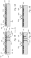
- Figure 1a shows a cross-sectional view of semiconductor substrate 100 of the method.
- the semiconductor substrate 100 has a front side 101 and a back side 103.
- the axis Y denotes a vertical direction corresponding to a normal direction with respect to the front side 101 of the semiconductor substrate 100.
- the axis X denotes a first horizontal direction along the front side 101 and the back side 103 of the semiconductor substrate 100 and the axis Z denotes a second horizontal direction along the front side 101 and the back side 103 of the semiconductor substrate 100, perpendicular to the first direction X.
- the relative dimensions of the shown elements such as the height, width or thickness of elements, is merely schematic and may, for the purpose of illustrational clarity, differ from a physical structure.
- Figure 1a shows that the semiconductor substrate 100 comprises a lower portion 102 and upper portion 104 along the Y direction.
- the lower portion 102 of the semiconductor substrate 100 may be any conventional substrate, suitable for semiconductor processing.
- the lower portion 102 may for instance be a semiconductor substrate.
- the lower portion 102 may comprise silicon (Si).
- the lower portion 102 may comprise germanium (Ge).
- the lower portion 102 may be a Si substrate, a Ge substrate, a SiGe substrate.
- Other examples include a silicon-on-insulator (SOI) substrate, a GeOl substrate or a SiGeOl substrate.
- SOI silicon-on-insulator
- Figure 1a shows that the front side 101 of the semiconductor substrate is provided with a plurality of device areas 110.
- two device areas 110a and 110b are shown.
- the front side 101 of semiconductor substrate 100 may be provided with any number of device areas 110, e.g. outside the illustrated region.
- the plurality of the device areas 110a and 110b, shown in Figure 1a are formed in the upper portion 104 of the semiconductor substrate 100.
- the plurality of the device areas 110 a and 110b may be formed in the lower 102 and upper portion 104 of the semiconductor substrate 100.
- Figure 1a shows an example wherein the device areas 110a and 110b are transistors fabricated by the conventional semiconductor fabrication processing.
- Figure 1a shows the device areas 110a and 110b after the FEOL and BEOL processing wherein metal interconnects 108 are formed and the device areas 110a and 110b are embedded in a dielectric layer 109.
- Other examples of device areas are memory elements such as random access memory (RAM) and NAND memory, microelectromechanical systems (MEMS), optical devices and radio frequency devices.
- RAM random access memory
- MEMS microelectromechanical systems
- the device areas 110, metal interconnects 108 and the dielectric layer 109 may be formed in a manner which per se is known in the art e.g. conventional semiconductor device fabrication processing.
- the device areas 110, metal interconnects 108 and the dielectric layer 109 may be formed of materials which per se is known in the art.
- the metal interconnects 108 may be formed of copper (Cu) and the dielectric layer 104 may be formed of SiO x or any low-k dielectric material.
- the semiconductor substrate 100 further comprises a plurality of through substrate vias 130.
- three through substrate vias 130a, 130b, and 130c are shown under the device area 110b.
- the semiconductor substrate 110 may be provided with any number of through substrate vias under any device area, e.g. inside and/or outside the illustrated region.
- the through substrate vias 130 extend through semiconductor substrate 100 i.e. along the Y direction.
- the through substrate vias 130 may have sizes in a range of 0.1 to 20 ⁇ m along the X and Z directions.
- the through substrate vias 130 may have a height in a range of 0.3 to 300 ⁇ m along the Y direction.
- the through substrate vias 130 may penetrate the semiconductor substrate 100 to a depth in a range of 0.3 to 300 ⁇ m along the Y direction.
- Figure 1a shows that the through substrate vias 130 extend through the upper 104 and the lower 102 portions of the semiconductor substrate 100.
- Figure 1a also shows that the three through substrate vias 130a, 130b, and 130c have different heights in the lower portion 102 of the semiconductor substrate 100.
- the through substrate vias 130 may be formed in a manner which per se is known in the art. Examples of the through substrate vias 130 are the through Si vias (TSV) used in conventional semiconductor device fabrication processing.
- TSV through Si vias
- the through substrate vias 130 may be formed of e.g. copper (Cu).
- Figure 1a further shows that the plurality of device areas 110, provided on the front side 101 of the semiconductor substrate, are separated by trench areas or separation areas 120.
- Figure 1a shows two of such trench areas 120a and 120b.
- the trench area 120b is arranged adjacent to the device area 110b and another device area (outside the illustrated region).
- the trench area 120a is arranged between the adjacent device areas 110a and 110b.
- the trench area 120a is arranged on the opposite side of the device area 110b along the X direction.
- a width of the trench areas 120 along the X direction may be in a range of 0.5 to 50 ⁇ m.
- the trench areas 120a and 120b shown in Figure 1a extend along the Z direction.
- the semiconductor substrate 100 may comprise trench areas 120 extending along other directions.
- the semiconductor substrate 100 may comprise trench areas 120 extending along the X direction.
- the method comprises defining, from the front side 101 of the semiconductor substrate 100, at least one trench 140 to be formed between the adjacent device areas 110.
- the step of defining the at least one trench 140 may be performed in any other manner which per se is known in the art such as laser scribing, blade cutting or plasma etching.
- the step of the defining the at least one trench 140 to be formed between adjacent device areas 110 may preferably include forming a photoresist 145 on the front side 101 of the semiconductor substrate 110.
- the photoresist 145 may be formed in a manner which per se in known in the art such as spin coating.
- the photoresist 145 may be formed of a positive or a negative photoresist.
- the photoresist 145 may only cover the plurality of device areas 110.
- the photoresist 145 may cover both the plurality of device areas 110 and the trench areas 120, as shown in Figure 2a .
- the method may proceed by patterning the photoresist 145 thereby defining the at least one trench 140 between the adjacent device areas 110.
- the step of patterning the photoresist 145 may be performed in manner which per se is known in the art such as using an electron beam lithography or UV lithography.
- the photoresist 145 may be removed, subsequent to the step of patterning the photoresist 145 and defining the at least one trench 140 between the adjacent device areas 110.
- the photoresist 145 may not be removed, subsequent to the step of patterning the photoresist 145 and defining the at least one trench 140 between the adjacent device areas 110.
- the at least one trench 140 may comprise two parallel trenches 140 extending between the adjacent device areas 110.
- Figure 2a shows that one trench 140c is defined in the trench area 120b and two trenches 140a and 140b are defined in the trench area 120a.
- the two parallel trenches 140a and 140b are defined between the adjacent device areas 110a and 110b.
- the trench 140c and the parallel trenches 140a and 140b shown in Figure 2a extend along the Z direction.
- the parallel trenches 140 may be defined e.g. when the trench areas 120 comprises additional structures such as metal lines or test structures.
- the parallel trenches 140 may define scribe lines.
- a width of the at least one trench 140 may be in a range of 1 to 100 ⁇ m.
- the method proceeds by forming the at least one trench 140, from the front side 101 of the semiconductor substrate 100.
- the step of the forming the at least one trench 140 may include etching the at least one trench 140, from the front side 101 of the semiconductor substrate 100, using the photoresist 145 as an etch mask.
- the step of forming the at least one trench 140, from the front side 101 of the semiconductor substrate 100 may be performed in a single step or in different steps.
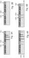
- Figure 3a and 4a show that the step of forming the at least one trench 140, from the front side 101 of the semiconductor substrate 100 is performed in two steps, using the photoresist 145 as an etch mask.
- Figure 3a shows the trenches 140a, 140b and 140c, subsequent to an etching step through the upper portion 104 of semiconductor substrate 100, using the photoresist 145 as an etch mask.
- Figure 4a shows the trenches 140a, 140b and 140c, subsequent to an etching step through the lower portion 102 of semiconductor substrate 100, using the photoresist 145 as an etch mask.
- the step of forming the at least one trench by etching may be performed in a manner which per se is known in the art such as wet etching or dry etching.
- An example of techniques used for the dry etching is Bosch process.
- examples of the etchant used are oxidizer plus fluoride (HF/HNO 3 ) or alkaline solutions such as TMAH, NH 4 OH or Met(OH) x .
- Figure 4a shows that the trenches 140a, 140b, and 140c are formed such that a major portion 106a of a thickness 106 of the semiconductor substrate 100 is removed.
- Figure 4a shows that a minor portion 106b of the thickness 106 of the semiconductor substrate 100 is left underneath the trenches 140a, 140b, and 140c.
- the minor portion of the thickness of the semiconductor substrate underneath the at least one trench may have a thickness in a range of 10 to 100 ⁇ m.
- the photoresist 145 if present, may be removed subsequent to the step of forming the at least one trench 140.
- the photoresist 145 if present, may not be removed subsequent to the step of forming the at least one trench 140.
- Figure 5a shows the semiconductor substrate 100 wherein the photoresist 145 is removed subsequent to the step of forming the at least one trench 140.
- the method proceeds by arranging a protective layer 150 on the front side 101 of the semiconductor substrate 100.
- the protective layer 150 covers at least a plurality of device areas 110.
- the protective layer 150 may cover a plurality of device areas 110 and a plurality of trench areas 120.
- Figure 6a shows that the protective layer 150 covers the device areas 110a and 110b and the trench areas 120a and 120b.
- the step of arranging the protective layer 150 may comprise depositing a bonding material 156 on the front side 101 of the semiconductor substrate 100.
- the step of arranging the protective layer 150 may further comprise attaching a carrier wafer 158 to the bonding material 156.
- the bonding material 156 may comprise a release layer 152 and a protective layer 154.
- Figure 6a shows that the release layer 152 is deposited on the front side 101 of the semiconductor substrate 100.
- Figure 6a further shows that the protective layer 154 is deposited on the release layer 152.
- the protective layer 154 may be deposited on the front side101 of the semiconductor substrate 100 and the release layer 152 may be deposited on the protective layer 154.
- the bonding material 156, the release layer 152, and the protective layer 154 may be deposited in a manner which per se is known in the art such as spin coating or vapor deposition.
- a thickness of the bonding material 156 along the Y direction may be in a range of 5 to 100 ⁇ m.
- a thickness of the release layer 152 along the Y direction may be in a range of 0.05 to 10 ⁇ m.
- a thickness of the protective layer 154 along the Y direction may be in a range of 1 to 99 ⁇ m.
- An example of the bonding material 156 is BrewerBond 220.
- An example of the release layer 152 is BrewerBond 701.
- An example of the protective layer 154 is AZ10XT.
- the carrier wafer 158 may be a light transparent wafer such as glass or saphire.
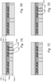
- the method proceeds by thinning the semiconductor substrate 100 from the back side 103 to reduce the thickness 106 of the semiconductor substrate 100.
- Figure 7a shows that a portion 106c of the minor 106b portion of the thickness 106 of the semiconductor substrate 100 is remained underneath the at least one trench 140, subsequent to the step of thinning.
- the step of thinning the semiconductor substrate 100 from the back side 103 may be performed in a manner which per se is known in the art such as any of or any combination of wet etching, dry etching, chemical mechanical polishing (CMP) or grinding.
- the step of thinning may be performed differently depending on e.g. a thickness of the substrate and a desired final result. For instance, in the step of thinning, up to several hundred micrometers of the thickness of the semiconductor substrate may be removed.
- the step of thinning the semiconductor substrate 100 further incudes revealing at least one through substrate via 130.
- Figure 7a shows that the through substrate via 130b and 130c are revealed.
- Figure 7a shows that the through substrate via 130c is exposed in the step of thinning.
- Figure 13b shows a close-up view of the through substrate via 130c, exposed in the step of thinning.
- Figure 13b further shows that the through substrate via 130c is covered by layer 132.
- the layer 132 may be formed of SiO x , Si 3 N 4 , SiCO, SiCN, AL 2 O 3 or similar materials.
- Figure 7a shows that the through substrate via 130b protrudes from the back side 103 of the semiconductor substrate 100 in the step of thinning.
- Figure 13c shows a close-up view of the through substrate via 130b, protruding from the back side 103 of the semiconductor substrate 100.
- the through substrate vias 130 may protrude from the back side 103 of the semiconductor substrate 100 when the step of thinning is performed by a selective etching approach such as wet etching. However, in case that the step of thinning is performed by CMP or grinding, the through substrate vias 130 may become planarized i.e. may not protrude from the back side 103 of the semiconductor substrate 100.
- the step of thinning the semiconductor substrate 100 may further include not revealing one of the through substrate vias 130a, 130b and 130c.
- Figure 7a shows that the through substrate via 130a is not revealed.
- Figure 13a shows a close-up view of the through substrate via 130a, not revealed in the step of thinning.
- Such un-revealed through substrate vias 130 such as the through substrate via 130a shown in Figure 7a may be revealed.
- This may be performed by forming, from the back side 103 of the semiconductor substrate 100, an opening underneath at least one through substrate via 130 to reveal the at least one through substrate via 130.
- Figure 14 shows an opening formed, from the back side 103 of the semiconductor substrate 100, underneath the through substrate via 130a.
- Figure 15 shows that the layer 132 is removed, from the back side 103 of the semiconductor substrate 100, to expose the through substrate via 130a.
- the method proceeds by processing the back side 103 of the semiconductor substrate 100 to form at least one contact 160, the contact 160 contacting at least one through substrate via 130.
- the processing of the back side 103 of the semiconductor substrate 100 to form the at least one contact 160 may include forming a passivation layer 134 on the back side 103 of the semiconductor substrate 100.
- the step of forming the passivation layer 134 may be performed on all the through substrate vias 130.
- Figures 16a, 16b, and 16c respectively show that a passivation layer 134 is formed on the back side 103 of the semiconductor substrate 100 on the revealed through substrate via 130a (revealed through the opening formation), the exposed through substrate via 130c, and the protruded through substrate via 130b.
- the step of forming the passivation layer 134 may be performed in a manner which per se is known in the art such as deposition.
- the passivation layer 134 may be formed of e.g. SiO x .
- a thickness of the passivation layer 134 may be in a range of 5 to 100 nm.
- the processing of the back side 103 of the semiconductor substrate 100 to form the at least one contact 160 may proceed by patterning the passivation layer 134 underneath the at least one through substrate via 130 to form an opening.
- the opening may expose at least a portion of the at least one through substrate via 130.
- Figure 17a, 17b, and 17c respectively show that the opening is formed exposing at least a portion of the at least one through substrate via 130a, 130c, and 130b.
- the step of patterning the passivation layer 134 to form an opening may be performed in a manner which per se is known in the art. For instance, the step of patterning the passivation layer 134 to form an opening for the through substrate vias 130b and 130c may be performed by CMP.
- the step of patterning the passivation layer 134 to form an opening for the through substrate via 130a may be performed by depositing a photoresist layer on the back side 103 of the semiconductor substrate 100 and lithographically patterning the photoresist layer.
- the processing of the back side 103 of the semiconductor substrate 100 to form the at least one contact 160 may further proceed by forming a contact 160 contacting the exposed portion of the at least one through substrate via 130.
- Figure 8 shows the semiconductor substrate 100, subsequent to the step of forming the at least one contact 160.
- Figures 18a, 18b and 18c show close-up views of the contacts 160 contacting the respective through substrate vias 130a, 130c, and 130b.
- the step of forming the contact 160 may be performed in a manner which per se is known is the art such as electroplating, atomic layer deposition, ALD, chemical vapor deposition, CVD, or physical vapor deposition, PVD.
- the contact 160 may be formed of any one of or any combination of Cu, Ni, Co, Sn, and Pb.
- a thickness of the contact 160 may be in a range of 1 to 100 ⁇ m.
- the method proceeds by etching, from the back side 103 of the semiconductor substrate 100, through the minor portion 106b of the thickness 106 of the semiconductor substrate 100 underneath the at least one trench 140.
- the step of etching separates the semiconductor substrate 100 into a plurality of device areas 110 arranged underneath the protective layer 150.
- Figures 9 and 10 show two examples of etching, from the back side 103 of the semiconductor substrate 100, through the minor portion 106b of the thickness 106 of the semiconductor substrate 100 underneath the at least one trench 140.
- a separate opening 146 is formed from the back side 103 of the semiconductor substrate 100 underneath each of the parallel trenches 140a and 140b.
- a common opening 148 is formed from the back side 103 of the semiconductor substrate 100 underneath the parallel trenches 140a and 140b.
- the step of etching, from the back side 103 of the semiconductor substrate 100 underneath the at least one trench 140 may be performed in a manner which per se is known in the art.
- the method may proceed by dicing the previously separated semiconductor substrate 100 into the plurality of dies 170.
- the step of dicing the semiconductor substrate 100 into the plurality of dies 170 may include separating the bonding material 156 of the protective layer 150 from the front side 101 of the semiconductor substrate 100.
- the bonding material 156 comprises the release layer 152 and the protective layer 154
- the step of dicing the semiconductor substrate 100 into the plurality of dies 170 may include separating the release layer 152 and the protective layer 154 from the front side 101 of the semiconductor substrate 100. Separating of the release layer 152 and the protective layer 154 from the front side 101 of the semiconductor substrate 100 may be done by wet or dry etching. This is schematically shown in Figure 11 that a die 170a has been formed by separating the release layer 152 and the protective layer 154 from the front side 101 of the semiconductor substrate 100.
- the step of dicing the semiconductor substrate 100 into the plurality of dies 170 may alternatively include separating the bonding material 156 of the protective layer 150 from the carrier wafer 158.
- the bonding material 156 of the protective layer 150 may remain on the front side 101 of the semiconductor substrate 100.
- Figure 12 shows that the bonding material 156 comprises the release layer 152 and the protective layer 154, the protective layer 154 is formed on the front side 101 of the semiconductor and the release layer 152 is formed on the protective layer 154.
- a die 170b has been formed by separating the protective layer 154 from the release layer 152 and the carrier wafer 158.
- Figure 12 shows that the protective layer 154 has remained on the front side of the die 170b i.e. the front side of the die 170b is protected by the protective layer 154.
- the step of separating the bonding material 156 of the protective layer 150 may be performed in a manner which per se is known in the art. For instance, in the case that the carrier wafer is a UV light transparent wafer and the bonding material 156 is photosensitive material, the step of separating bonding material 156 of the protective layer 150 may be performed by shining a laser light on the carrier wafer 158 such that the laser light becomes focused on the photosensitive bonding material 156. The step of separating the bonding material 156 of the protective layer 150 may also be performed by means of peal bonding. The carrier wafer 158 may be cleaned subsequent to the step of dicing. The carrier wafer 158 may be reused.
- the semiconductor substrate 100 may be diced into a plurality of the dies 170. Each formed die 170 may be picked up by e.g. a die handling robot. The formed dies 170 may be cleaned, subsequent to the step of dicing. The formed dies 170 may be stacked on each other, subsequent to the step of dicing. The formed dies 170 may be populated onto another semiconductor substrate, subsequent to the step of dicing.
- FIG. 1b-7b show initial steps of dicing the semiconductor substrate 200, similar to the Figures 1a-7a discussed above in relation to the semiconductor substrate 100.
- Figure 7c and 7d schematically illustrate steps of forming a plurality of substrate through vias 230 from the back side 203 of the semiconductor substrate 200. Further steps of dicing the semiconductor substrate 200 into a plurality of dies 270 may be performed in accordance with the steps discussed in relation to Figures 8-18 .
Landscapes
- Internal Circuitry In Semiconductor Integrated Circuit Devices (AREA)
- Dicing (AREA)
Description
- The present inventive concept relates to a method for dicing a semiconductor substrate into a plurality of dies.
- A type of semiconductor product comprises semiconductor devices which are stacked and packed into one package. Such semiconductor devices may be produced on one substrate and may be diced into dies, prior to stacking. The dicing of the semiconductor substrate may produce particles, due to mechanical separation of different dies. The particles may have sizes in the order of, or even larger than, the sizes of the semiconductor devices. The particles may stick on surfaces of the semiconductor devices and may form voids around them. Thereby, yield and functionality of the semiconductor products, formed by the devices contaminated by such particles, may be affected.
- An example of a method for dicing a semiconductor wafer is disclosed in
EP 3 531 447 A2 . The method comprises forming at least one trench in non-device regions of a first surface of a semiconductor wafer and forming at least one trench in non-circuit regions the first surface of the semiconductor wafer. The non-device regions are arranged between component positions and the component positions comprising at least two semiconductor devices for forming a circuit. A non-circuit region is arranged between a first device region comprising a first electronic device and a second device region comprising a second electronic device, a first metallization layer being arranged on the first surface in the first device region and in the second device region. A first polymer layer is applied to the first surface of a semiconductor wafer such that the trenches, edge regions of the component positions, edge regions of the first device regions and edge regions of the second device regions are covered with the first polymer layer. Portions of a second opposing surface of the semiconductor wafer are removed, revealing portions of the first polymer layer in the non-device regions and in the non-circuit regions to produce a worked second surface. The method further comprises applying a second metallization layer to the worked second surface and coupling the first electronic device to the second electronic device to form the circuit and inserting a separation line through the first polymer layer in the non-device regions to form a plurality of separate semiconductor dies comprising the circuit. - An object of the present inventive concept is to, at least partly, overcome one or more of the above-identified limitations of the prior art. In particular, an object of the present inventive concept is to provide a method which protects surfaces of the semiconductor devices during the dicing.
- According to an aspect of the present inventive concept there is provided a method for dicing a semiconductor substrate into a plurality of dies as defined in claim 1.
- The present inventive concept allows defining the at least one trench to be formed between adjacent device areas at desired areas with desired shapes such as square shape. The step of forming the at least one trench, from the front side of the semiconductor substrate, by removing a major portion of a thickness of the semiconductor substrate and leaving a minor portion of the thickness of the semiconductor substrate underneath the at least one trench allows forming the at least one trench while holding the adjacent device areas together. The step of arranging the protective layer on the front side of the semiconductor substrate allows protecting the front side of the semiconductor substrate during the following steps to be performed. The protective layer is arranged such that it covers at least a plurality of device areas. Thereby, the protective layer protects the front side of the semiconductor substrate during the following steps, particularly the dicing step, to be performed. In other words, the protective layer protects the front side of the semiconductor substrate against particles typically being formed during the dicing step and also against other contaminations. The protective layer may cover the at least one trench. The protective layer may not cover the at least one trench. The step of thinning the semiconductor substrate from the back side allows reducing a thickness of the semiconductor substrate including a thickness of the minor portion of the semiconductor substrate underneath the at least one trench. The steps of thinning and etching, from the back side of the semiconductor substrate, allow mechanical separation of the adjacent device areas while the adjacent device areas are held together by the protective layer. The step of processing the back side of the semiconductor substrate to form at least one contact, the contact contacting at least one through substrate via, allows forming contacts enabling contacting the device areas to be stacked and packed. The step of dicing allows separation of the plurality of device areas of the semiconductor substrate, obtained subsequent to the step of etching, into the plurality of dies. For instance, the step of dicing may comprise separation of the plurality of device areas of the semiconductor substrate from at least a portion of the protective layer arranged underneath. Thereby the step of dicing allows dicing the plurality of device areas of the semiconductor substrate into a plurality of dies. The step of dicing further allows singulation of dies one by one and hence provides an improved control and reliability compared to singulation of multiple dies attached to each other.
- By the "device areas" are hereby meant areas of the semiconductor substrate comprising devices. Examples of such devices may be transistors formed by conventional semiconductor fabrication processing such as front-end-of-line, FEOL, and back-end-of-line, BEOL, processing.
- By the "front side" is hereby meant an upper surface of the semiconductor substrate. By the "back side" is hereby meant a lower surface of the semiconductor substrate. In case of the semiconductor substrate comprises a stack of layers, the front side and the back side are respectively the uppermost and the lowermost surfaces.
- By the "through substrate vias" is hereby meant vias formed through the substrate such that the vias typically extend perpendicularly to the front side or the back side of the semiconductor substrate i.e. vias typically extending in a direction parallel to a normal direction of the front and the back side. An example of the through substrate vias is through silicon vias (TSV) which is the term commonly used when the substrate is made of silicon.
- By "on" is hereby meant above and in contact with. For instance, by arranging the protective layer on the front side of the semiconductor substrate is hereby meant that the protective layer is arranged above and in contact with the front side of the semiconductor substrate.
- By "underneath" is hereby meant below and in contact with. For instance, by leaving a minor portion of the thickness of the semiconductor substrate underneath the at least one trench is hereby meant leaving a minor portion of the thickness of the semiconductor substrate below and in contact with the at least one trench.
- By "die" is hereby meant a portion of the semiconductor substrate e.g. a device area separated from the semiconductor substrate. Separation of the die may e.g. be performed by separating the semiconductor substrate into the plurality of device areas, obtained subsequent to the step of etching, from the protective layer arranged underneath. The die may comprise a device area or a plurality of device areas. The die may have various shapes and sizes.
- A width of the at least one trench may be in a range of 0.5 to 50 µm. This trench width range may facilitate dicing the semiconductor substrate into the plurality of dies and singulation of the dies one by one i.e. the trench width range may prevent unintentional attachment of dies to each other.
- The minor portion of the thickness of the semiconductor substrate underneath the at least one trench may have a thickness in a range of 0.3 to 100 µm. This thickness range may provide a sufficient mechanical support to hold the semiconductor substrate together prior to the step of arranging the protective layer. This thickness range may also facilitate the step of thinning the semiconductor substrate from the back side.
- The at least one trench may comprise two parallel trenches extending between the adjacent device areas. The parallel trenches may be advantageous when the semiconductor substrate comprises additional structures arranged between the adjacent device areas such as test structures. In the case of having test structures, only one trench may not allow a complete removal of the test structures i.e. the test structures may remain e.g. along edges of the dies, subsequent to the step of dicing. Thereby, the dies may comprise metals and other materials of the test structures along their edges. The presence of the metals and other materials of the test structures in the dies may in turn lead to contamination of the dies e.g. due to corrosion of the test structures metals. Moreover, the parallel trenches may be advantageous and facilitate singulation of the semiconductor substrate into dies.
- The step of arranging the protective layer may comprises depositing a bonding material on the front side of the semiconductor substrate and attaching a carrier wafer to the bonding material. The bonding material may allow bonding of the semiconductor substrate to the carrier wafer. The bonding material may allow separation of the front side of the semiconductor substrate from the carrier wafer in the step of dicing.
- The bonding layer may comprise a layer or a stack of layers. For instance, the bonding layer may comprise a release layer and a protective layer arranged on the front side of the semiconductor substrate. The release layer may allow separation of the front side of the semiconductor substrate in the step of dicing. An example of a release layer may be a photosensitive layer.
- The carrier wafer may provide a mechanical support for the semiconductor substrate during the steps of thinning, processing, etching and dicing. The carrier wafer may be cleaned and reused, subsequent to the step of the dicing.
- The step of dicing the semiconductor substrate into the plurality of dies may include separating the bonding material of the protective layer from the front side of the semiconductor substrate. Thereby, no or little bonding material may remain on the front side of the semiconductor substrate, subsequent to the step of dicing.
- In the case that the bonding material comprises a release layer and a protective layer, separating the bonding material of the protective layer from the front side of the semiconductor substrate may be done by arranging the release layer on the front side of the semiconductor substrate and arranging the protective layer on the release layer. Thereby, no or little protective layer may remain on the front side of the semiconductor, subsequent to the step of dicing. In this case, the protective layer may act as a glue to adhere the release layer to the carrier wafer.
- The step of dicing the semiconductor substrate into the plurality of dies may include separating the bonding material of the protective layer from the carrier wafer leaving the bonding material of the protective layer on the front side of the semiconductor substrate. Thereby, the front side of the semiconductor substrate may be protected by the bonding material, subsequent to the step of dicing.
- In the case that the bonding material comprises the release layer and the protective layer, leaving the bonding material of the protective layer on the front side of the semiconductor substrate may be done by arranging the protective layer on the front side of the semiconductor substrate and arranging the release layer on the protective layer. Thereby, the protective layer may remain on the front side of the semiconductor substrate, subsequent to the step of dicing.
- The step of the defining the at least one trench to be formed between adjacent device areas may include forming a photoresist on the front side of the semiconductor substrate covering a plurality of device areas, and patterning the photoresist thereby defining the at least one trench between the adjacent device areas. The steps of forming and patterning the photoresist are compatible with the conventional semiconductor fabrication processing and may provide improved flexibility and reliability in defining the at least one trench. In addition, the photoresist may remain on the front side of the semiconductor substrate and may protect the front side of the semiconductor substrate during the subsequent method steps to be performed.
- The step of the forming the at least one trench may include etching the at least one trench, from the front side of the semiconductor substrate, using the photoresist as an etch mask. Thereby the photoresist may be used not only for patterning the front side of the semiconductor substrate but also for masking the front side of the semiconductor substrate in the step of etching. This may in turn decrease a time and a number of method steps for dicing the semiconductor substrate at least by eliminating a step of defining a mask.
- The step of thinning the semiconductor substrate further includes revealing at least one through substrate via.
- The least one through substrate via may protrude from the back side of the semiconductor substrate in the step of thinning. An example of an advantage brought by revealing at least one through substrate via is that no additional step may be needed, prior to the step of the processing the back side of the semiconductor substrate to form the at least one contact.
- The method may further comprise, prior to the step of processing the back side of the semiconductor substrate, forming, from the back side of the semiconductor substrate, an opening underneath at least one through substrate via to reveal the at least one through substrate via. This step is advantageous when the plurality of the through substrate vias of the semiconductor substrate have different heights or penetration depths into the semiconductor substrate since this step may facilitate revealing the at least one through substrate via, prior to the step of the processing the back side of the semiconductor substrate to form the at least one contact.
- The step of processing the back side of the semiconductor substrate to form the at least one contact may further include forming a passivation layer on the back side of the semiconductor substrate, patterning the passivation layer underneath the at least one through substrate via to form an opening exposing at least a portion of the at least one through substrate via, and forming a contact contacting the exposed portion of the at least one through substrate via. Thereby the formed contact may facilitate steps of contacting a stack of dies to be formed, subsequent to the step of dicing the semiconductor substrate into the plurality of dies.
- The carrier wafer may be a light transparent wafer such as an ultraviolet, UV, light transparent wafer. A light transparent carrier wafer may be used with a photosensitive bonding material. This may in turn facilitate separating the bonding material from the front side of the semiconductor substrate. In the case that the bonding material comprises the release layer and the protective layer and that the release layer is arranged on the front side of the semiconductor substrate and the protective layer is arranged on the release layer, this may in turn facilitate separating the release layer from the front side of the semiconductor substrate.
- This may alternatively facilitate separating the bonding material from the carrier wafer. In the case that the bonding material comprises the release layer and the protective layer and that the protective layer is arranged on the front side of the semiconductor substrate and the release layer is arranged on the protective layer, this may in turn facilitate separating the release layer from the protective layer.
- The semiconductor substrate may comprise Si. The semiconductor substrate may be suitable for the conventional semiconductor fabrication processing.
- The above, as well as additional objects, features and advantages of the present inventive concept, will be better understood through the following illustrative and non-limiting detailed description, with reference to the appended drawings. In the drawings like reference numerals will be used for like elements unless stated otherwise.
-
Figures 1-18 schematically illustrate various steps of a method for dicing a semiconductor substrate into a plurality of dies. -
Figures 1-7 schematically illustrate two variations: a first variation (shown inFigures 1a-7a ) schematically illustrates initial steps of dicing a semiconductor substrate wherein the semiconductor substrate comprises a plurality of through substrate vias, and a second variation (shown inFigures 1b-7b ) schematically illustrates initial steps of dicing a semiconductor substrate wherein the semiconductor substrate does not comprise through substrate vias.Figure 7c and 7d schematically illustrate steps of forming substrate through vias in the second variation.Figures 8-18 schematically illustrates other steps of dicing a semiconductor substrate which are common for both variations. - Various methods for dicing a semiconductor substrate into a plurality of dies will now be disclosed in connection with
Figures 1-18 . -
Figure 1a shows a cross-sectional view ofsemiconductor substrate 100 of the method. Thesemiconductor substrate 100 has afront side 101 and aback side 103. InFigure 1 , the axis Y denotes a vertical direction corresponding to a normal direction with respect to thefront side 101 of thesemiconductor substrate 100. The axis X denotes a first horizontal direction along thefront side 101 and theback side 103 of thesemiconductor substrate 100 and the axis Z denotes a second horizontal direction along thefront side 101 and theback side 103 of thesemiconductor substrate 100, perpendicular to the first direction X. It should be noted that in the drawings the relative dimensions of the shown elements, such as the height, width or thickness of elements, is merely schematic and may, for the purpose of illustrational clarity, differ from a physical structure. -
Figure 1a shows that thesemiconductor substrate 100 comprises alower portion 102 andupper portion 104 along the Y direction. Thelower portion 102 of thesemiconductor substrate 100 may be any conventional substrate, suitable for semiconductor processing. Thelower portion 102 may for instance be a semiconductor substrate. Thelower portion 102 may comprise silicon (Si). Thelower portion 102 may comprise germanium (Ge). Thelower portion 102 may be a Si substrate, a Ge substrate, a SiGe substrate. Other examples include a silicon-on-insulator (SOI) substrate, a GeOl substrate or a SiGeOl substrate. -
Figure 1a shows that thefront side 101 of the semiconductor substrate is provided with a plurality of device areas 110. InFigure 1a and the following figures, twodevice areas front side 101 ofsemiconductor substrate 100 may be provided with any number of device areas 110, e.g. outside the illustrated region. The plurality of thedevice areas Figure 1a , are formed in theupper portion 104 of thesemiconductor substrate 100. The plurality of thedevice areas 110 a and 110bmay be formed in the lower 102 andupper portion 104 of thesemiconductor substrate 100. -
Figure 1a shows an example wherein thedevice areas Figure 1a shows thedevice areas metal interconnects 108 are formed and thedevice areas dielectric layer 109. Other examples of device areas are memory elements such as random access memory (RAM) and NAND memory, microelectromechanical systems (MEMS), optical devices and radio frequency devices. The device areas 110,metal interconnects 108 and thedielectric layer 109 may be formed in a manner which per se is known in the art e.g. conventional semiconductor device fabrication processing. The device areas 110,metal interconnects 108 and thedielectric layer 109 may be formed of materials which per se is known in the art. As an example, the metal interconnects 108 may be formed of copper (Cu) and thedielectric layer 104 may be formed of SiOx or any low-k dielectric material. - The
semiconductor substrate 100 further comprises a plurality of through substrate vias 130. InFigure 1a and the following figures, three throughsubstrate vias device area 110b. However, it should be noted that the semiconductor substrate 110 may be provided with any number of through substrate vias under any device area, e.g. inside and/or outside the illustrated region. The through substrate vias 130 extend throughsemiconductor substrate 100 i.e. along the Y direction. The through substrate vias 130 may have sizes in a range of 0.1 to 20 µm along the X and Z directions. The through substrate vias 130 may have a height in a range of 0.3 to 300 µm along the Y direction. In other words, the through substrate vias 130 may penetrate thesemiconductor substrate 100 to a depth in a range of 0.3 to 300 µm along the Y direction.Figure 1a shows that the through substrate vias 130 extend through the upper 104 and the lower 102 portions of thesemiconductor substrate 100.Figure 1a also shows that the three throughsubstrate vias lower portion 102 of thesemiconductor substrate 100. The through substrate vias 130 may be formed in a manner which per se is known in the art. Examples of the through substrate vias 130 are the through Si vias (TSV) used in conventional semiconductor device fabrication processing. The through substrate vias 130 may be formed of e.g. copper (Cu). -
Figure 1a further shows that the plurality of device areas 110, provided on thefront side 101 of the semiconductor substrate, are separated by trench areas or separation areas 120.Figure 1a shows two ofsuch trench areas trench area 120b is arranged adjacent to thedevice area 110b and another device area (outside the illustrated region). Thetrench area 120a is arranged between theadjacent device areas trench area 120a is arranged on the opposite side of thedevice area 110b along the X direction. A width of the trench areas 120 along the X direction may be in a range of 0.5 to 50 µm. Thetrench areas Figure 1a extend along the Z direction. However, thesemiconductor substrate 100 may comprise trench areas 120 extending along other directions. For instance, thesemiconductor substrate 100 may comprise trench areas 120 extending along the X direction. - Now referring to
Figure 2a , the method comprises defining, from thefront side 101 of thesemiconductor substrate 100, at least one trench 140 to be formed between the adjacent device areas 110. The step of defining the at least one trench 140 may be performed in any other manner which per se is known in the art such as laser scribing, blade cutting or plasma etching. The step of the defining the at least one trench 140 to be formed between adjacent device areas 110 may preferably include forming aphotoresist 145 on thefront side 101 of the semiconductor substrate 110. Thephotoresist 145 may be formed in a manner which per se in known in the art such as spin coating. Thephotoresist 145 may be formed of a positive or a negative photoresist. Thephotoresist 145 may only cover the plurality of device areas 110. Thephotoresist 145 may cover both the plurality of device areas 110 and the trench areas 120, as shown inFigure 2a . - The method may proceed by patterning the
photoresist 145 thereby defining the at least one trench 140 between the adjacent device areas 110. The step of patterning thephotoresist 145 may be performed in manner which per se is known in the art such as using an electron beam lithography or UV lithography. Thephotoresist 145 may be removed, subsequent to the step of patterning thephotoresist 145 and defining the at least one trench 140 between the adjacent device areas 110. Thephotoresist 145 may not be removed, subsequent to the step of patterning thephotoresist 145 and defining the at least one trench 140 between the adjacent device areas 110. - The at least one trench 140 may comprise two parallel trenches 140 extending between the adjacent device areas 110.
Figure 2a shows that onetrench 140c is defined in thetrench area 120b and twotrenches trench area 120a. The twoparallel trenches adjacent device areas trench 140c and theparallel trenches Figure 2a extend along the Z direction. The parallel trenches 140 may be defined e.g. when the trench areas 120 comprises additional structures such as metal lines or test structures. The parallel trenches 140 may define scribe lines. A width of the at least one trench 140 may be in a range of 1 to 100 µm. - The method proceeds by forming the at least one trench 140, from the
front side 101 of thesemiconductor substrate 100. The step of the forming the at least one trench 140 may include etching the at least one trench 140, from thefront side 101 of thesemiconductor substrate 100, using thephotoresist 145 as an etch mask. The step of forming the at least one trench 140, from thefront side 101 of thesemiconductor substrate 100 may be performed in a single step or in different steps.Figure 3a and 4a show that the step of forming the at least one trench 140, from thefront side 101 of thesemiconductor substrate 100 is performed in two steps, using thephotoresist 145 as an etch mask.Figure 3a shows thetrenches upper portion 104 ofsemiconductor substrate 100, using thephotoresist 145 as an etch mask.Figure 4a shows thetrenches lower portion 102 ofsemiconductor substrate 100, using thephotoresist 145 as an etch mask. The step of forming the at least one trench by etching may be performed in a manner which per se is known in the art such as wet etching or dry etching. An example of techniques used for the dry etching is Bosch process. In the case of wet etching, examples of the etchant used are oxidizer plus fluoride (HF/HNO3) or alkaline solutions such as TMAH, NH4OH or Met(OH)x. - In addition,
Figure 4a shows that thetrenches major portion 106a of athickness 106 of thesemiconductor substrate 100 is removed. In other words,Figure 4a shows that aminor portion 106b of thethickness 106 of thesemiconductor substrate 100 is left underneath thetrenches photoresist 145, if present, may be removed subsequent to the step of forming the at least one trench 140. Thephotoresist 145, if present, may not be removed subsequent to the step of forming the at least one trench 140.Figure 5a shows thesemiconductor substrate 100 wherein thephotoresist 145 is removed subsequent to the step of forming the at least one trench 140. - The method proceeds by arranging a
protective layer 150 on thefront side 101 of thesemiconductor substrate 100. Theprotective layer 150 covers at least a plurality of device areas 110. Theprotective layer 150 may cover a plurality of device areas 110 and a plurality of trench areas 120.Figure 6a shows that theprotective layer 150 covers thedevice areas trench areas - The step of arranging the
protective layer 150 may comprise depositing abonding material 156 on thefront side 101 of thesemiconductor substrate 100. The step of arranging theprotective layer 150 may further comprise attaching acarrier wafer 158 to thebonding material 156. - The
bonding material 156 may comprise arelease layer 152 and aprotective layer 154.Figure 6a shows that therelease layer 152 is deposited on thefront side 101 of thesemiconductor substrate 100.Figure 6a further shows that theprotective layer 154 is deposited on therelease layer 152. Alternatively, theprotective layer 154 may be deposited on the front side101 of thesemiconductor substrate 100 and therelease layer 152 may be deposited on theprotective layer 154. Thebonding material 156, therelease layer 152, and theprotective layer 154 may be deposited in a manner which per se is known in the art such as spin coating or vapor deposition. A thickness of thebonding material 156 along the Y direction may be in a range of 5 to 100 µm. A thickness of therelease layer 152 along the Y direction may be in a range of 0.05 to 10 µm. A thickness of theprotective layer 154 along the Y direction may be in a range of 1 to 99 µm. An example of thebonding material 156 is BrewerBond 220. An example of therelease layer 152 is BrewerBond 701. An example of theprotective layer 154 is AZ10XT. Thecarrier wafer 158 may be a light transparent wafer such as glass or saphire. - The method proceeds by thinning the
semiconductor substrate 100 from theback side 103 to reduce thethickness 106 of thesemiconductor substrate 100.Figure 7a shows that aportion 106c of the minor 106b portion of thethickness 106 of thesemiconductor substrate 100 is remained underneath the at least one trench 140, subsequent to the step of thinning. The step of thinning thesemiconductor substrate 100 from theback side 103 may be performed in a manner which per se is known in the art such as any of or any combination of wet etching, dry etching, chemical mechanical polishing (CMP) or grinding. The step of thinning may be performed differently depending on e.g. a thickness of the substrate and a desired final result. For instance, in the step of thinning, up to several hundred micrometers of the thickness of the semiconductor substrate may be removed. - The step of thinning the
semiconductor substrate 100 further incudes revealing at least one through substrate via 130.Figure 7a shows that the through substrate via 130b and 130c are revealed.Figure 7a shows that the through substrate via 130c is exposed in the step of thinning.Figure 13b shows a close-up view of the through substrate via 130c, exposed in the step of thinning.Figure 13b further shows that the through substrate via 130c is covered bylayer 132. For instance, thelayer 132 may be formed of SiOx, Si3N4, SiCO, SiCN, AL2O3 or similar materials. -
Figure 7a shows that the through substrate via 130b protrudes from theback side 103 of thesemiconductor substrate 100 in the step of thinning.Figure 13c shows a close-up view of the through substrate via 130b, protruding from theback side 103 of thesemiconductor substrate 100. The through substrate vias 130 may protrude from theback side 103 of thesemiconductor substrate 100 when the step of thinning is performed by a selective etching approach such as wet etching. However, in case that the step of thinning is performed by CMP or grinding, the through substrate vias 130 may become planarized i.e. may not protrude from theback side 103 of thesemiconductor substrate 100. - The step of thinning the
semiconductor substrate 100 may further include not revealing one of the throughsubstrate vias Figure 7a shows that the through substrate via 130a is not revealed.Figure 13a shows a close-up view of the through substrate via 130a, not revealed in the step of thinning. Such un-revealed through substrate vias 130 such as the through substrate via 130a shown inFigure 7a may be revealed. This may be performed by forming, from theback side 103 of thesemiconductor substrate 100, an opening underneath at least one through substrate via 130 to reveal the at least one through substrate via 130.Figure 14 shows an opening formed, from theback side 103 of thesemiconductor substrate 100, underneath the through substrate via 130a.Figure 15 shows that thelayer 132 is removed, from theback side 103 of thesemiconductor substrate 100, to expose the through substrate via 130a. - Now referring to
Figure 8 , the method proceeds by processing theback side 103 of thesemiconductor substrate 100 to form at least onecontact 160, thecontact 160 contacting at least one through substrate via 130. The processing of theback side 103 of thesemiconductor substrate 100 to form the at least onecontact 160 may include forming apassivation layer 134 on theback side 103 of thesemiconductor substrate 100. The step of forming thepassivation layer 134 may be performed on all the through substrate vias 130.Figures 16a, 16b, and 16c respectively show that apassivation layer 134 is formed on theback side 103 of thesemiconductor substrate 100 on the revealed through substrate via 130a (revealed through the opening formation), the exposed through substrate via 130c, and the protruded through substrate via 130b. The step of forming thepassivation layer 134 may be performed in a manner which per se is known in the art such as deposition. Thepassivation layer 134 may be formed of e.g. SiOx. A thickness of thepassivation layer 134 may be in a range of 5 to 100 nm. - The processing of the
back side 103 of thesemiconductor substrate 100 to form the at least onecontact 160 may proceed by patterning thepassivation layer 134 underneath the at least one through substrate via 130 to form an opening. The opening may expose at least a portion of the at least one through substrate via 130.Figure 17a, 17b, and 17c respectively show that the opening is formed exposing at least a portion of the at least one through substrate via 130a, 130c, and 130b. The step of patterning thepassivation layer 134 to form an opening may be performed in a manner which per se is known in the art. For instance, the step of patterning thepassivation layer 134 to form an opening for the throughsubstrate vias passivation layer 134 to form an opening for the through substrate via 130a (revealed through the opening formation) may be performed by depositing a photoresist layer on theback side 103 of thesemiconductor substrate 100 and lithographically patterning the photoresist layer. - The processing of the
back side 103 of thesemiconductor substrate 100 to form the at least onecontact 160 may further proceed by forming acontact 160 contacting the exposed portion of the at least one through substrate via 130.Figure 8 shows thesemiconductor substrate 100, subsequent to the step of forming the at least onecontact 160.Figures 18a, 18b and 18c show close-up views of thecontacts 160 contacting the respective throughsubstrate vias contact 160 may be performed in a manner which per se is known is the art such as electroplating, atomic layer deposition, ALD, chemical vapor deposition, CVD, or physical vapor deposition, PVD. Thecontact 160 may be formed of any one of or any combination of Cu, Ni, Co, Sn, and Pb. A thickness of thecontact 160 may be in a range of 1 to 100 µm. - The method proceeds by etching, from the
back side 103 of thesemiconductor substrate 100, through theminor portion 106b of thethickness 106 of thesemiconductor substrate 100 underneath the at least one trench 140. Thereby the step of etching separates thesemiconductor substrate 100 into a plurality of device areas 110 arranged underneath theprotective layer 150.Figures 9 and 10 show two examples of etching, from theback side 103 of thesemiconductor substrate 100, through theminor portion 106b of thethickness 106 of thesemiconductor substrate 100 underneath the at least one trench 140. InFigure 9 , aseparate opening 146 is formed from theback side 103 of thesemiconductor substrate 100 underneath each of theparallel trenches Figure 10 , acommon opening 148 is formed from theback side 103 of thesemiconductor substrate 100 underneath theparallel trenches back side 103 of thesemiconductor substrate 100 underneath the at least one trench 140 may be performed in a manner which per se is known in the art. - The method may proceed by dicing the previously separated
semiconductor substrate 100 into the plurality of dies 170. The step of dicing thesemiconductor substrate 100 into the plurality of dies 170 may include separating thebonding material 156 of theprotective layer 150 from thefront side 101 of thesemiconductor substrate 100. In the case that thebonding material 156 comprises therelease layer 152 and theprotective layer 154, the step of dicing thesemiconductor substrate 100 into the plurality of dies 170 may include separating therelease layer 152 and theprotective layer 154 from thefront side 101 of thesemiconductor substrate 100. Separating of therelease layer 152 and theprotective layer 154 from thefront side 101 of thesemiconductor substrate 100 may be done by wet or dry etching. This is schematically shown inFigure 11 that adie 170a has been formed by separating therelease layer 152 and theprotective layer 154 from thefront side 101 of thesemiconductor substrate 100. - The step of dicing the
semiconductor substrate 100 into the plurality of dies 170 may alternatively include separating thebonding material 156 of theprotective layer 150 from thecarrier wafer 158. Thebonding material 156 of theprotective layer 150 may remain on thefront side 101 of thesemiconductor substrate 100. An example of this is shown inFigure 12. Figure 12 shows that thebonding material 156 comprises therelease layer 152 and theprotective layer 154, theprotective layer 154 is formed on thefront side 101 of the semiconductor and therelease layer 152 is formed on theprotective layer 154. As shown inFigure 12 , adie 170b has been formed by separating theprotective layer 154 from therelease layer 152 and thecarrier wafer 158. In other words,Figure 12 shows that theprotective layer 154 has remained on the front side of thedie 170b i.e. the front side of thedie 170b is protected by theprotective layer 154. - The step of separating the
bonding material 156 of theprotective layer 150 may be performed in a manner which per se is known in the art. For instance, in the case that the carrier wafer is a UV light transparent wafer and thebonding material 156 is photosensitive material, the step of separatingbonding material 156 of theprotective layer 150 may be performed by shining a laser light on thecarrier wafer 158 such that the laser light becomes focused on thephotosensitive bonding material 156. The step of separating thebonding material 156 of theprotective layer 150 may also be performed by means of peal bonding. Thecarrier wafer 158 may be cleaned subsequent to the step of dicing. Thecarrier wafer 158 may be reused. - The
semiconductor substrate 100 may be diced into a plurality of the dies 170. Each formed die 170 may be picked up by e.g. a die handling robot. The formed dies 170 may be cleaned, subsequent to the step of dicing. The formed dies 170 may be stacked on each other, subsequent to the step of dicing. The formed dies 170 may be populated onto another semiconductor substrate, subsequent to the step of dicing. - The method described above may be applied to a
semiconductor substrate 200 having afront side 201, aback side 203, and a plurality of device areas 210 on thefront side 201 i.e. not having a plurality of through substrate vias.Figures 1b-7b show initial steps of dicing thesemiconductor substrate 200, similar to theFigures 1a-7a discussed above in relation to thesemiconductor substrate 100.Figure 7c and 7d schematically illustrate steps of forming a plurality of substrate throughvias 230 from theback side 203 of thesemiconductor substrate 200. Further steps of dicing thesemiconductor substrate 200 into a plurality of dies 270 may be performed in accordance with the steps discussed in relation toFigures 8-18 . - In the above the inventive concept has mainly been described with reference to a limited number of examples. However, as is readily appreciated by a person skilled in the art, other examples than the ones disclosed above are equally possible within the scope of the inventive concept, as defined by the appended claims.
Claims (13)
- A method for dicing a semiconductor substrate (100) into a plurality of dies (170), wherein the semiconductor substrate having a front side (101) provided with a plurality of device areas (110), a back side (103), and a plurality of through substrate vias (130), the method comprising the following order of steps:defining, from the front side (101) of the semiconductor substrate (100), at least one trench (140) to be formed between adjacent device areas (110a, 110b),forming the at least one trench (140), from the front side (101) of the semiconductor substrate (100), such that a major portion (106a) of a thickness (106) of the semiconductor substrate (100) is removed in the at least one trench (140), thereby leaving a minor (106b) portion of the thickness (106) of the semiconductor substrate (100) underneath the at least one trench (140),arranging, subsequent to forming the at least one trench (140), a protective layer (150) on the front side (101) of the semiconductor substrate (100), the protective layer (150) covering at least a plurality of device areas (110),thinning, subsequent to arranging the protective layer (150), the semiconductor substrate (100) from the back side (103) to reduce the thickness (106) of the semiconductor substrate (100), whereby at least one through substrate via (130) is revealed while a portion (106c) of the minor (106b) portion of the thickness (106) of the semiconductor substrate (100) is remained underneath the at least one trench (140),processing the back side (103) of the semiconductor substrate 100 to form at least one contact (160), the contact (160) contacting at least one revealed through substrate via (130),etching, subsequent to processing the back side (103), from the back side (103) of the semiconductor substrate (100), through the remaining portion (106c) of the minor portion (106b) of the thickness (106) of the semiconductor substrate (100) underneath the at least one trench (140), thereby separating the semiconductor substrate into a plurality of device areas (110) arranged underneath the protective layer (150), anddicing the semiconductor substrate (100) into the plurality of dies (170).
- The method according to claim 1, wherein a width of the at least one trench (140) is in a range of 0.5 to 50 µm.
- The method according to claim 1 or 2, wherein the minor portion of the thickness (106b) of the semiconductor substrate (100) underneath the at least one trench (140) has a thickness in a range of 0.3 to 100 µm.
- The method according to any one of the preceding claims, wherein the at least one trench (140) comprises two parallel trenches (140a, 140b) extending between the adjacent device areas.
- The method according to claim 1, wherein the step of arranging the protective layer (150) comprises:depositing a bonding material (156) on the front side (101) of the semiconductor substrate (100), andattaching a carrier wafer (158) to the bonding material (156).
- The method according to claim 5, wherein the step of dicing the semiconductor substrate (100) into the plurality of dies (170) includes separating the bonding material (156) of the protective layer (150) from the front side (101) of the semiconductor substrate (100).
- The method according to claim 5, wherein the step of dicing the semiconductor substrate (100) into the plurality of dies (170) includes separating the bonding material (156) of the protective layer (150) from the carrier wafer (158) leaving the bonding material (156) of the protective layer (150) on the front side (101) of the semiconductor substrate (100).
- The method according to any one of the preceding claims, wherein the step of the defining the at least one trench (140) to be formed between adjacent device areas (110) includes:forming a photoresist (145) on the front side (101) of the semiconductor substrate (100) covering a plurality of device areas (110), andpatterning the photoresist (145) thereby defining the at least one trench (140) between the adjacent device areas (110).
- The method according to claim 8, wherein the step of the forming the at least one trench (140) includes etching the at least one trench (140), from the front side (101) of the semiconductor substrate (100), using the photoresist (145) as an etch mask.
- The method according to claims 1-9, wherein the method further comprises, prior to the step of processing the back side (103) of the semiconductor substrate (100), forming, from the back side (103) of the semiconductor substrate (100), an opening underneath at least one through substrate via to reveal at least one through substrate via not revealed in the step of thinning.
- The method according to any one of the preceding claims, wherein the step of processing the back side (103) of the semiconductor substrate (100) to form the at least one contact (160) further includes:forming a passivation layer (134) on the back side (103) of the semiconductor substrate (100),patterning the passivation layer (134) underneath the at least one through substrate via (130) to form an opening exposing at least a portion of the at least one through substrate via (130), andforming a contact (160) contacting the exposed portion of the at least one through substrate via (130).
- The method according to claims 5-11, wherein the carrier wafer (158) is a light transparent wafer.
- The method according to any one of the preceding claims, wherein the semiconductor substrate (100) comprises Si.
Priority Applications (2)
| Application Number | Priority Date | Filing Date | Title |
|---|---|---|---|
| EP19200554.4A EP3799112B1 (en) | 2019-09-30 | 2019-09-30 | Method for dicing a semiconductor substrate into a plurality of dies |
| US17/038,737 US11476162B2 (en) | 2019-09-30 | 2020-09-30 | Method for dicing a semiconductor substrate into a plurality of dies |
Applications Claiming Priority (1)
| Application Number | Priority Date | Filing Date | Title |
|---|---|---|---|
| EP19200554.4A EP3799112B1 (en) | 2019-09-30 | 2019-09-30 | Method for dicing a semiconductor substrate into a plurality of dies |
Publications (2)
| Publication Number | Publication Date |
|---|---|
| EP3799112A1 EP3799112A1 (en) | 2021-03-31 |
| EP3799112B1 true EP3799112B1 (en) | 2024-02-21 |
Family
ID=68109126
Family Applications (1)
| Application Number | Title | Priority Date | Filing Date |
|---|---|---|---|
| EP19200554.4A Active EP3799112B1 (en) | 2019-09-30 | 2019-09-30 | Method for dicing a semiconductor substrate into a plurality of dies |
Country Status (2)
| Country | Link |
|---|---|
| US (1) | US11476162B2 (en) |
| EP (1) | EP3799112B1 (en) |
Families Citing this family (6)
| Publication number | Priority date | Publication date | Assignee | Title |
|---|---|---|---|---|
| US11436132B2 (en) | 2020-03-16 | 2022-09-06 | International Business Machines Corporation | Stress test impact isolation and mapping |
| US11194703B2 (en) | 2020-03-16 | 2021-12-07 | International Business Machines Corporation | System testing infrastructure for analyzing soft failures in active environment |
| US11194704B2 (en) | 2020-03-16 | 2021-12-07 | International Business Machines Corporation | System testing infrastructure using combinatorics |
| US11609842B2 (en) | 2020-03-16 | 2023-03-21 | International Business Machines Corporation | System testing infrastructure for analyzing and preventing soft failure in active environment |
| US20230245926A1 (en) * | 2020-06-24 | 2023-08-03 | Nippon Telegraph And Telephone Corporation | Method for Manufacturing Semiconductor Device |
| WO2022063431A1 (en) * | 2020-09-22 | 2022-03-31 | Kulicke & Soffa Netherlands B.V. | Reusable die catch materials, reusable die release materials, related die transfer systems, and methods of using the same |
Family Cites Families (14)
| Publication number | Priority date | Publication date | Assignee | Title |
|---|---|---|---|---|
| US6573156B1 (en) | 2001-12-13 | 2003-06-03 | Omm, Inc. | Low defect method for die singulation and for structural support for handling thin film devices |
| US6908784B1 (en) * | 2002-03-06 | 2005-06-21 | Micron Technology, Inc. | Method for fabricating encapsulated semiconductor components |
| JP4377300B2 (en) * | 2004-06-22 | 2009-12-02 | Necエレクトロニクス株式会社 | Semiconductor wafer and semiconductor device manufacturing method |
| US7265034B2 (en) * | 2005-02-18 | 2007-09-04 | Taiwan Semiconductor Manufacturing Company, Ltd. | Method of cutting integrated circuit chips from wafer by ablating with laser and cutting with saw blade |
| US7482251B1 (en) | 2006-08-10 | 2009-01-27 | Impinj, Inc. | Etch before grind for semiconductor die singulation |
| US8941182B2 (en) * | 2011-06-07 | 2015-01-27 | Globalfoundries Inc. | Buried sublevel metallizations for improved transistor density |
| US8642385B2 (en) * | 2011-08-09 | 2014-02-04 | Alpha & Omega Semiconductor, Inc. | Wafer level package structure and the fabrication method thereof |
| US8906803B2 (en) | 2013-03-15 | 2014-12-09 | Sandia Corporation | Method of forming through substrate vias (TSVs) and singulating and releasing die having the TSVs from a mechanical support substrate |
| US9196568B2 (en) * | 2013-10-01 | 2015-11-24 | Infineon Technologies Ag | Arrangement and method for manufacturing the same |
| EP2913848A1 (en) | 2014-02-27 | 2015-09-02 | ams AG | Dicing method |
| US9589812B2 (en) | 2014-11-06 | 2017-03-07 | Fuji Xerox Co., Ltd. | Fabrication method of semiconductor piece |
| US9741620B2 (en) * | 2015-06-24 | 2017-08-22 | Invensas Corporation | Structures and methods for reliable packages |
| TW202524641A (en) * | 2016-01-15 | 2025-06-16 | 荷蘭商庫力克及索發荷蘭公司 | Placing ultra-small or ultra-thin discrete components |
| EP3531446B1 (en) * | 2018-02-23 | 2024-04-03 | Infineon Technologies Austria AG | Semiconductor module, electronic component and method of manufacturing a semiconductor module |
-
2019
- 2019-09-30 EP EP19200554.4A patent/EP3799112B1/en active Active
-
2020
- 2020-09-30 US US17/038,737 patent/US11476162B2/en active Active
Also Published As
| Publication number | Publication date |
|---|---|
| US11476162B2 (en) | 2022-10-18 |
| EP3799112A1 (en) | 2021-03-31 |
| US20210098299A1 (en) | 2021-04-01 |
Similar Documents
| Publication | Publication Date | Title |
|---|---|---|
| EP3799112B1 (en) | Method for dicing a semiconductor substrate into a plurality of dies | |
| US7566634B2 (en) | Method for chip singulation | |
| US9768089B2 (en) | Wafer stack protection seal | |
| EP2530709B1 (en) | Method of producing a semiconductor wafer | |
| US11764096B2 (en) | Method for semiconductor die edge protection and semiconductor die separation | |
| KR100855015B1 (en) | Packaged integrated circuit and manufacturing method thereof | |
| CN106340491A (en) | Method for use in manufacturing a semiconductor device die | |
| WO2014144597A1 (en) | Method of forming through substrate vias (tsvs) and singulating and releasing die having the tsvs from a mechanical support substrate | |
| US12046513B2 (en) | Die corner protection by using polymer deposition technology | |
| CN109256334A (en) | Method for manufacturing the IC chip laterally to insulate | |
| CN113078109A (en) | Manufacturing method of semiconductor structure and semiconductor structure | |
| CN108122855B (en) | Semiconductor structures and semiconductor manufacturing methods | |
| EP2908335A1 (en) | Dicing method | |
| US8129805B2 (en) | Microelectromechanical system (MEMS) device and methods for fabricating the same | |
| US11710661B2 (en) | Semiconductor packages and methods of packaging semiconductor devices | |
| US20120126391A1 (en) | Methods for Embedding Conducting Material and Devices Resulting from Said Methods | |
| US12550414B2 (en) | Wafer-level die singulation using buried sacrificial structure | |
| EP4564404A1 (en) | A method for removing residues from a substrate surface | |
| US11670549B2 (en) | Semiconductor packages without debris | |
| EP1670055A1 (en) | Method for chip singulation | |
| EP1641038B1 (en) | Method for chip singulation | |
| WO2017190060A1 (en) | Methods for singulation and packaging | |
| CN117995671A (en) | Multilayer stacked wafer cutting method and multilayer stacked structure | |
| CN114582803A (en) | Method for manufacturing semiconductor tube core and semiconductor device |
Legal Events
| Date | Code | Title | Description |
|---|---|---|---|
| PUAI | Public reference made under article 153(3) epc to a published international application that has entered the european phase |
Free format text: ORIGINAL CODE: 0009012 |
|
| STAA | Information on the status of an ep patent application or granted ep patent |
Free format text: STATUS: THE APPLICATION HAS BEEN PUBLISHED |
|
| AK | Designated contracting states |
Kind code of ref document: A1 Designated state(s): AL AT BE BG CH CY CZ DE DK EE ES FI FR GB GR HR HU IE IS IT LI LT LU LV MC MK MT NL NO PL PT RO RS SE SI SK SM TR |
|
| AX | Request for extension of the european patent |
Extension state: BA ME |
|
| STAA | Information on the status of an ep patent application or granted ep patent |
Free format text: STATUS: REQUEST FOR EXAMINATION WAS MADE |
|
| 17P | Request for examination filed |
Effective date: 20210921 |
|
| RBV | Designated contracting states (corrected) |
Designated state(s): AL AT BE BG CH CY CZ DE DK EE ES FI FR GB GR HR HU IE IS IT LI LT LU LV MC MK MT NL NO PL PT RO RS SE SI SK SM TR |
|
| GRAP | Despatch of communication of intention to grant a patent |
Free format text: ORIGINAL CODE: EPIDOSNIGR1 |
|
| STAA | Information on the status of an ep patent application or granted ep patent |
Free format text: STATUS: GRANT OF PATENT IS INTENDED |
|
| RIC1 | Information provided on ipc code assigned before grant |
Ipc: H01L 23/00 20060101ALI20231017BHEP Ipc: H01L 21/56 20060101ALI20231017BHEP Ipc: H01L 21/78 20060101AFI20231017BHEP |
|
| INTG | Intention to grant announced |
Effective date: 20231108 |
|
| RAP3 | Party data changed (applicant data changed or rights of an application transferred) |
Owner name: IMEC VZW |
|
| P01 | Opt-out of the competence of the unified patent court (upc) registered |
Effective date: 20231127 |
|
| GRAS | Grant fee paid |
Free format text: ORIGINAL CODE: EPIDOSNIGR3 |
|
| GRAA | (expected) grant |
Free format text: ORIGINAL CODE: 0009210 |
|
| STAA | Information on the status of an ep patent application or granted ep patent |
Free format text: STATUS: THE PATENT HAS BEEN GRANTED |
|
| AK | Designated contracting states |
Kind code of ref document: B1 Designated state(s): AL AT BE BG CH CY CZ DE DK EE ES FI FR GB GR HR HU IE IS IT LI LT LU LV MC MK MT NL NO PL PT RO RS SE SI SK SM TR |
|
| REG | Reference to a national code |
Ref country code: GB Ref legal event code: FG4D |
|
| REG | Reference to a national code |
Ref country code: CH Ref legal event code: EP |
|
| REG | Reference to a national code |
Ref country code: DE Ref legal event code: R096 Ref document number: 602019046822 Country of ref document: DE |
|
| REG | Reference to a national code |
Ref country code: IE Ref legal event code: FG4D |
|
| REG | Reference to a national code |
Ref country code: LT Ref legal event code: MG9D |
|
| REG | Reference to a national code |
Ref country code: NL Ref legal event code: MP Effective date: 20240221 |
|
| PG25 | Lapsed in a contracting state [announced via postgrant information from national office to epo] |
Ref country code: IS Free format text: LAPSE BECAUSE OF FAILURE TO SUBMIT A TRANSLATION OF THE DESCRIPTION OR TO PAY THE FEE WITHIN THE PRESCRIBED TIME-LIMIT Effective date: 20240621 |
|
| PG25 | Lapsed in a contracting state [announced via postgrant information from national office to epo] |
Ref country code: LT Free format text: LAPSE BECAUSE OF FAILURE TO SUBMIT A TRANSLATION OF THE DESCRIPTION OR TO PAY THE FEE WITHIN THE PRESCRIBED TIME-LIMIT Effective date: 20240221 |
|
| PG25 | Lapsed in a contracting state [announced via postgrant information from national office to epo] |
Ref country code: GR Free format text: LAPSE BECAUSE OF FAILURE TO SUBMIT A TRANSLATION OF THE DESCRIPTION OR TO PAY THE FEE WITHIN THE PRESCRIBED TIME-LIMIT Effective date: 20240522 |
|
| REG | Reference to a national code |
Ref country code: AT Ref legal event code: MK05 Ref document number: 1659862 Country of ref document: AT Kind code of ref document: T Effective date: 20240221 |
|
| PG25 | Lapsed in a contracting state [announced via postgrant information from national office to epo] |
Ref country code: HR Free format text: LAPSE BECAUSE OF FAILURE TO SUBMIT A TRANSLATION OF THE DESCRIPTION OR TO PAY THE FEE WITHIN THE PRESCRIBED TIME-LIMIT Effective date: 20240221 Ref country code: NL Free format text: LAPSE BECAUSE OF FAILURE TO SUBMIT A TRANSLATION OF THE DESCRIPTION OR TO PAY THE FEE WITHIN THE PRESCRIBED TIME-LIMIT Effective date: 20240221 Ref country code: RS Free format text: LAPSE BECAUSE OF FAILURE TO SUBMIT A TRANSLATION OF THE DESCRIPTION OR TO PAY THE FEE WITHIN THE PRESCRIBED TIME-LIMIT Effective date: 20240521 |
|
| PG25 | Lapsed in a contracting state [announced via postgrant information from national office to epo] |
Ref country code: ES Free format text: LAPSE BECAUSE OF FAILURE TO SUBMIT A TRANSLATION OF THE DESCRIPTION OR TO PAY THE FEE WITHIN THE PRESCRIBED TIME-LIMIT Effective date: 20240221 |
|
| PG25 | Lapsed in a contracting state [announced via postgrant information from national office to epo] |
Ref country code: AT Free format text: LAPSE BECAUSE OF FAILURE TO SUBMIT A TRANSLATION OF THE DESCRIPTION OR TO PAY THE FEE WITHIN THE PRESCRIBED TIME-LIMIT Effective date: 20240221 |
|
| PG25 | Lapsed in a contracting state [announced via postgrant information from national office to epo] |
Ref country code: RS Free format text: LAPSE BECAUSE OF FAILURE TO SUBMIT A TRANSLATION OF THE DESCRIPTION OR TO PAY THE FEE WITHIN THE PRESCRIBED TIME-LIMIT Effective date: 20240521 Ref country code: NO Free format text: LAPSE BECAUSE OF FAILURE TO SUBMIT A TRANSLATION OF THE DESCRIPTION OR TO PAY THE FEE WITHIN THE PRESCRIBED TIME-LIMIT Effective date: 20240521 Ref country code: NL Free format text: LAPSE BECAUSE OF FAILURE TO SUBMIT A TRANSLATION OF THE DESCRIPTION OR TO PAY THE FEE WITHIN THE PRESCRIBED TIME-LIMIT Effective date: 20240221 Ref country code: LT Free format text: LAPSE BECAUSE OF FAILURE TO SUBMIT A TRANSLATION OF THE DESCRIPTION OR TO PAY THE FEE WITHIN THE PRESCRIBED TIME-LIMIT Effective date: 20240221 Ref country code: IS Free format text: LAPSE BECAUSE OF FAILURE TO SUBMIT A TRANSLATION OF THE DESCRIPTION OR TO PAY THE FEE WITHIN THE PRESCRIBED TIME-LIMIT Effective date: 20240621 Ref country code: HR Free format text: LAPSE BECAUSE OF FAILURE TO SUBMIT A TRANSLATION OF THE DESCRIPTION OR TO PAY THE FEE WITHIN THE PRESCRIBED TIME-LIMIT Effective date: 20240221 Ref country code: GR Free format text: LAPSE BECAUSE OF FAILURE TO SUBMIT A TRANSLATION OF THE DESCRIPTION OR TO PAY THE FEE WITHIN THE PRESCRIBED TIME-LIMIT Effective date: 20240522 Ref country code: FI Free format text: LAPSE BECAUSE OF FAILURE TO SUBMIT A TRANSLATION OF THE DESCRIPTION OR TO PAY THE FEE WITHIN THE PRESCRIBED TIME-LIMIT Effective date: 20240221 Ref country code: ES Free format text: LAPSE BECAUSE OF FAILURE TO SUBMIT A TRANSLATION OF THE DESCRIPTION OR TO PAY THE FEE WITHIN THE PRESCRIBED TIME-LIMIT Effective date: 20240221 Ref country code: BG Free format text: LAPSE BECAUSE OF FAILURE TO SUBMIT A TRANSLATION OF THE DESCRIPTION OR TO PAY THE FEE WITHIN THE PRESCRIBED TIME-LIMIT Effective date: 20240221 Ref country code: AT Free format text: LAPSE BECAUSE OF FAILURE TO SUBMIT A TRANSLATION OF THE DESCRIPTION OR TO PAY THE FEE WITHIN THE PRESCRIBED TIME-LIMIT Effective date: 20240221 |
|
| PG25 | Lapsed in a contracting state [announced via postgrant information from national office to epo] |
Ref country code: PL Free format text: LAPSE BECAUSE OF FAILURE TO SUBMIT A TRANSLATION OF THE DESCRIPTION OR TO PAY THE FEE WITHIN THE PRESCRIBED TIME-LIMIT Effective date: 20240221 Ref country code: PT Free format text: LAPSE BECAUSE OF FAILURE TO SUBMIT A TRANSLATION OF THE DESCRIPTION OR TO PAY THE FEE WITHIN THE PRESCRIBED TIME-LIMIT Effective date: 20240621 |
|
| PG25 | Lapsed in a contracting state [announced via postgrant information from national office to epo] |
Ref country code: SE Free format text: LAPSE BECAUSE OF FAILURE TO SUBMIT A TRANSLATION OF THE DESCRIPTION OR TO PAY THE FEE WITHIN THE PRESCRIBED TIME-LIMIT Effective date: 20240221 Ref country code: PT Free format text: LAPSE BECAUSE OF FAILURE TO SUBMIT A TRANSLATION OF THE DESCRIPTION OR TO PAY THE FEE WITHIN THE PRESCRIBED TIME-LIMIT Effective date: 20240621 Ref country code: PL Free format text: LAPSE BECAUSE OF FAILURE TO SUBMIT A TRANSLATION OF THE DESCRIPTION OR TO PAY THE FEE WITHIN THE PRESCRIBED TIME-LIMIT Effective date: 20240221 Ref country code: LV Free format text: LAPSE BECAUSE OF FAILURE TO SUBMIT A TRANSLATION OF THE DESCRIPTION OR TO PAY THE FEE WITHIN THE PRESCRIBED TIME-LIMIT Effective date: 20240221 |
|
| PG25 | Lapsed in a contracting state [announced via postgrant information from national office to epo] |
Ref country code: DK Free format text: LAPSE BECAUSE OF FAILURE TO SUBMIT A TRANSLATION OF THE DESCRIPTION OR TO PAY THE FEE WITHIN THE PRESCRIBED TIME-LIMIT Effective date: 20240221 |
|
| PG25 | Lapsed in a contracting state [announced via postgrant information from national office to epo] |
Ref country code: SM Free format text: LAPSE BECAUSE OF FAILURE TO SUBMIT A TRANSLATION OF THE DESCRIPTION OR TO PAY THE FEE WITHIN THE PRESCRIBED TIME-LIMIT Effective date: 20240221 |
|
| PG25 | Lapsed in a contracting state [announced via postgrant information from national office to epo] |
Ref country code: EE Free format text: LAPSE BECAUSE OF FAILURE TO SUBMIT A TRANSLATION OF THE DESCRIPTION OR TO PAY THE FEE WITHIN THE PRESCRIBED TIME-LIMIT Effective date: 20240221 Ref country code: CZ Free format text: LAPSE BECAUSE OF FAILURE TO SUBMIT A TRANSLATION OF THE DESCRIPTION OR TO PAY THE FEE WITHIN THE PRESCRIBED TIME-LIMIT Effective date: 20240221 |
|
| PG25 | Lapsed in a contracting state [announced via postgrant information from national office to epo] |
Ref country code: SK Free format text: LAPSE BECAUSE OF FAILURE TO SUBMIT A TRANSLATION OF THE DESCRIPTION OR TO PAY THE FEE WITHIN THE PRESCRIBED TIME-LIMIT Effective date: 20240221 |
|
| PG25 | Lapsed in a contracting state [announced via postgrant information from national office to epo] |
Ref country code: SM Free format text: LAPSE BECAUSE OF FAILURE TO SUBMIT A TRANSLATION OF THE DESCRIPTION OR TO PAY THE FEE WITHIN THE PRESCRIBED TIME-LIMIT Effective date: 20240221 Ref country code: SK Free format text: LAPSE BECAUSE OF FAILURE TO SUBMIT A TRANSLATION OF THE DESCRIPTION OR TO PAY THE FEE WITHIN THE PRESCRIBED TIME-LIMIT Effective date: 20240221 Ref country code: RO Free format text: LAPSE BECAUSE OF FAILURE TO SUBMIT A TRANSLATION OF THE DESCRIPTION OR TO PAY THE FEE WITHIN THE PRESCRIBED TIME-LIMIT Effective date: 20240221 Ref country code: EE Free format text: LAPSE BECAUSE OF FAILURE TO SUBMIT A TRANSLATION OF THE DESCRIPTION OR TO PAY THE FEE WITHIN THE PRESCRIBED TIME-LIMIT Effective date: 20240221 Ref country code: DK Free format text: LAPSE BECAUSE OF FAILURE TO SUBMIT A TRANSLATION OF THE DESCRIPTION OR TO PAY THE FEE WITHIN THE PRESCRIBED TIME-LIMIT Effective date: 20240221 Ref country code: CZ Free format text: LAPSE BECAUSE OF FAILURE TO SUBMIT A TRANSLATION OF THE DESCRIPTION OR TO PAY THE FEE WITHIN THE PRESCRIBED TIME-LIMIT Effective date: 20240221 |
|
| REG | Reference to a national code |
Ref country code: DE Ref legal event code: R097 Ref document number: 602019046822 Country of ref document: DE |
|
| PG25 | Lapsed in a contracting state [announced via postgrant information from national office to epo] |
Ref country code: IT Free format text: LAPSE BECAUSE OF FAILURE TO SUBMIT A TRANSLATION OF THE DESCRIPTION OR TO PAY THE FEE WITHIN THE PRESCRIBED TIME-LIMIT Effective date: 20240221 |
|
| PLBE | No opposition filed within time limit |
Free format text: ORIGINAL CODE: 0009261 |
|
| STAA | Information on the status of an ep patent application or granted ep patent |
Free format text: STATUS: NO OPPOSITION FILED WITHIN TIME LIMIT |
|
| PG25 | Lapsed in a contracting state [announced via postgrant information from national office to epo] |
Ref country code: IT Free format text: LAPSE BECAUSE OF FAILURE TO SUBMIT A TRANSLATION OF THE DESCRIPTION OR TO PAY THE FEE WITHIN THE PRESCRIBED TIME-LIMIT Effective date: 20240221 |
|
| 26N | No opposition filed |
Effective date: 20241122 |
|
| PG25 | Lapsed in a contracting state [announced via postgrant information from national office to epo] |
Ref country code: MC Free format text: LAPSE BECAUSE OF FAILURE TO SUBMIT A TRANSLATION OF THE DESCRIPTION OR TO PAY THE FEE WITHIN THE PRESCRIBED TIME-LIMIT Effective date: 20240221 Ref country code: SI Free format text: LAPSE BECAUSE OF FAILURE TO SUBMIT A TRANSLATION OF THE DESCRIPTION OR TO PAY THE FEE WITHIN THE PRESCRIBED TIME-LIMIT Effective date: 20240221 |
|
| REG | Reference to a national code |
Ref country code: CH Ref legal event code: PL |
|
| PG25 | Lapsed in a contracting state [announced via postgrant information from national office to epo] |
Ref country code: LU Free format text: LAPSE BECAUSE OF NON-PAYMENT OF DUE FEES Effective date: 20240930 |
|
| GBPC | Gb: european patent ceased through non-payment of renewal fee |
Effective date: 20240930 |
|
| PG25 | Lapsed in a contracting state [announced via postgrant information from national office to epo] |
Ref country code: GB Free format text: LAPSE BECAUSE OF NON-PAYMENT OF DUE FEES Effective date: 20240930 |
|
| REG | Reference to a national code |
Ref country code: BE Ref legal event code: MM Effective date: 20240930 |
|
| PG25 | Lapsed in a contracting state [announced via postgrant information from national office to epo] |
Ref country code: BE Free format text: LAPSE BECAUSE OF NON-PAYMENT OF DUE FEES Effective date: 20240930 |
|
| PG25 | Lapsed in a contracting state [announced via postgrant information from national office to epo] |
Ref country code: FR Free format text: LAPSE BECAUSE OF NON-PAYMENT OF DUE FEES Effective date: 20240930 |
|
| PG25 | Lapsed in a contracting state [announced via postgrant information from national office to epo] |
Ref country code: CH Free format text: LAPSE BECAUSE OF NON-PAYMENT OF DUE FEES Effective date: 20240930 |
|
| PG25 | Lapsed in a contracting state [announced via postgrant information from national office to epo] |
Ref country code: IE Free format text: LAPSE BECAUSE OF NON-PAYMENT OF DUE FEES Effective date: 20240930 |
|
| PGFP | Annual fee paid to national office [announced via postgrant information from national office to epo] |
Ref country code: DE Payment date: 20250820 Year of fee payment: 7 |
|
| REG | Reference to a national code |
Ref country code: DE Ref legal event code: R079 Ref document number: 602019046822 Country of ref document: DE Free format text: PREVIOUS MAIN CLASS: H01L0021780000 Ipc: H10P0058000000 |
|
| PG25 | Lapsed in a contracting state [announced via postgrant information from national office to epo] |
Ref country code: CY Free format text: LAPSE BECAUSE OF FAILURE TO SUBMIT A TRANSLATION OF THE DESCRIPTION OR TO PAY THE FEE WITHIN THE PRESCRIBED TIME-LIMIT; INVALID AB INITIO Effective date: 20190930 |
|
| PG25 | Lapsed in a contracting state [announced via postgrant information from national office to epo] |
Ref country code: HU Free format text: LAPSE BECAUSE OF FAILURE TO SUBMIT A TRANSLATION OF THE DESCRIPTION OR TO PAY THE FEE WITHIN THE PRESCRIBED TIME-LIMIT; INVALID AB INITIO Effective date: 20190930 |