EP3400608B1 - Elektronenstrahlvorrichtung umfassend ein austastsystem mit verbesserter wärmeverteilung - Google Patents
Elektronenstrahlvorrichtung umfassend ein austastsystem mit verbesserter wärmeverteilung Download PDFInfo
- Publication number
- EP3400608B1 EP3400608B1 EP17736363.7A EP17736363A EP3400608B1 EP 3400608 B1 EP3400608 B1 EP 3400608B1 EP 17736363 A EP17736363 A EP 17736363A EP 3400608 B1 EP3400608 B1 EP 3400608B1
- Authority
- EP
- European Patent Office
- Prior art keywords
- aperture
- electron beam
- locus
- plates
- pattern
- Prior art date
- Legal status (The legal status is an assumption and is not a legal conclusion. Google has not performed a legal analysis and makes no representation as to the accuracy of the status listed.)
- Active
Links
Images







Classifications
-
- H—ELECTRICITY
- H01—ELECTRIC ELEMENTS
- H01J—ELECTRIC DISCHARGE TUBES OR DISCHARGE LAMPS
- H01J37/00—Discharge tubes with provision for introducing objects or material to be exposed to the discharge, e.g. for the purpose of examination or processing thereof
- H01J37/02—Details
- H01J37/04—Arrangements of electrodes and associated parts for generating or controlling the discharge, e.g. electron-optical arrangement or ion-optical arrangement
- H01J37/045—Beam blanking or chopping, i.e. arrangements for momentarily interrupting exposure to the discharge
-
- G—PHYSICS
- G03—PHOTOGRAPHY; CINEMATOGRAPHY; ANALOGOUS TECHNIQUES USING WAVES OTHER THAN OPTICAL WAVES; ELECTROGRAPHY; HOLOGRAPHY
- G03F—PHOTOMECHANICAL PRODUCTION OF TEXTURED OR PATTERNED SURFACES, e.g. FOR PRINTING, FOR PROCESSING OF SEMICONDUCTOR DEVICES; MATERIALS THEREFOR; ORIGINALS THEREFOR; APPARATUS SPECIALLY ADAPTED THEREFOR
- G03F1/00—Originals for photomechanical production of textured or patterned surfaces, e.g., masks, photo-masks, reticles; Mask blanks or pellicles therefor; Containers specially adapted therefor; Preparation thereof
- G03F1/68—Preparation processes not covered by groups G03F1/20 - G03F1/50
- G03F1/82—Auxiliary processes, e.g. cleaning or inspecting
- G03F1/84—Inspecting
- G03F1/86—Inspecting by charged particle beam [CPB]
-
- G—PHYSICS
- G03—PHOTOGRAPHY; CINEMATOGRAPHY; ANALOGOUS TECHNIQUES USING WAVES OTHER THAN OPTICAL WAVES; ELECTROGRAPHY; HOLOGRAPHY
- G03F—PHOTOMECHANICAL PRODUCTION OF TEXTURED OR PATTERNED SURFACES, e.g. FOR PRINTING, FOR PROCESSING OF SEMICONDUCTOR DEVICES; MATERIALS THEREFOR; ORIGINALS THEREFOR; APPARATUS SPECIALLY ADAPTED THEREFOR
- G03F7/00—Photomechanical, e.g. photolithographic, production of textured or patterned surfaces, e.g. printing surfaces; Materials therefor, e.g. comprising photoresists; Apparatus specially adapted therefor
- G03F7/70—Microphotolithographic exposure; Apparatus therefor
- G03F7/708—Construction of apparatus, e.g. environment aspects, hygiene aspects or materials
- G03F7/7085—Detection arrangement, e.g. detectors of apparatus alignment possibly mounted on wafers, exposure dose, photo-cleaning flux, stray light, thermal load
-
- H—ELECTRICITY
- H01—ELECTRIC ELEMENTS
- H01J—ELECTRIC DISCHARGE TUBES OR DISCHARGE LAMPS
- H01J37/00—Discharge tubes with provision for introducing objects or material to be exposed to the discharge, e.g. for the purpose of examination or processing thereof
- H01J37/02—Details
- H01J37/04—Arrangements of electrodes and associated parts for generating or controlling the discharge, e.g. electron-optical arrangement or ion-optical arrangement
- H01J37/147—Arrangements for directing or deflecting the discharge along a desired path
-
- H—ELECTRICITY
- H01—ELECTRIC ELEMENTS
- H01J—ELECTRIC DISCHARGE TUBES OR DISCHARGE LAMPS
- H01J37/00—Discharge tubes with provision for introducing objects or material to be exposed to the discharge, e.g. for the purpose of examination or processing thereof
- H01J37/02—Details
- H01J37/04—Arrangements of electrodes and associated parts for generating or controlling the discharge, e.g. electron-optical arrangement or ion-optical arrangement
- H01J37/147—Arrangements for directing or deflecting the discharge along a desired path
- H01J37/1472—Deflecting along given lines
-
- H—ELECTRICITY
- H01—ELECTRIC ELEMENTS
- H01J—ELECTRIC DISCHARGE TUBES OR DISCHARGE LAMPS
- H01J37/00—Discharge tubes with provision for introducing objects or material to be exposed to the discharge, e.g. for the purpose of examination or processing thereof
- H01J37/02—Details
- H01J37/21—Means for adjusting the focus
-
- H—ELECTRICITY
- H10—SEMICONDUCTOR DEVICES; ELECTRIC SOLID-STATE DEVICES NOT OTHERWISE PROVIDED FOR
- H10P—GENERIC PROCESSES OR APPARATUS FOR THE MANUFACTURE OR TREATMENT OF DEVICES COVERED BY CLASS H10
- H10P74/00—Testing or measuring during manufacture or treatment of wafers, substrates or devices
- H10P74/20—Testing or measuring during manufacture or treatment of wafers, substrates or devices characterised by the properties tested or measured, e.g. structural or electrical properties
- H10P74/203—Structural properties, e.g. testing or measuring thicknesses, line widths, warpage, bond strengths or physical defects
-
- H—ELECTRICITY
- H10—SEMICONDUCTOR DEVICES; ELECTRIC SOLID-STATE DEVICES NOT OTHERWISE PROVIDED FOR
- H10P—GENERIC PROCESSES OR APPARATUS FOR THE MANUFACTURE OR TREATMENT OF DEVICES COVERED BY CLASS H10
- H10P74/00—Testing or measuring during manufacture or treatment of wafers, substrates or devices
- H10P74/23—Testing or measuring during manufacture or treatment of wafers, substrates or devices characterised by multiple measurements, corrections, marking or sorting processes
- H10P74/235—Testing or measuring during manufacture or treatment of wafers, substrates or devices characterised by multiple measurements, corrections, marking or sorting processes comprising optical enhancement of defects or not-directly-visible states
-
- H—ELECTRICITY
- H10—SEMICONDUCTOR DEVICES; ELECTRIC SOLID-STATE DEVICES NOT OTHERWISE PROVIDED FOR
- H10P—GENERIC PROCESSES OR APPARATUS FOR THE MANUFACTURE OR TREATMENT OF DEVICES COVERED BY CLASS H10
- H10P74/00—Testing or measuring during manufacture or treatment of wafers, substrates or devices
- H10P74/27—Structural arrangements therefor
-
- H—ELECTRICITY
- H01—ELECTRIC ELEMENTS
- H01J—ELECTRIC DISCHARGE TUBES OR DISCHARGE LAMPS
- H01J2237/00—Discharge tubes exposing object to beam, e.g. for analysis treatment, etching, imaging
- H01J2237/02—Details
- H01J2237/0203—Protection arrangements
- H01J2237/0213—Avoiding deleterious effects due to interactions between particles and tube elements
-
- H—ELECTRICITY
- H01—ELECTRIC ELEMENTS
- H01J—ELECTRIC DISCHARGE TUBES OR DISCHARGE LAMPS
- H01J2237/00—Discharge tubes exposing object to beam, e.g. for analysis treatment, etching, imaging
- H01J2237/04—Means for controlling the discharge
- H01J2237/045—Diaphragms
- H01J2237/0451—Diaphragms with fixed aperture
-
- H—ELECTRICITY
- H01—ELECTRIC ELEMENTS
- H01J—ELECTRIC DISCHARGE TUBES OR DISCHARGE LAMPS
- H01J2237/00—Discharge tubes exposing object to beam, e.g. for analysis treatment, etching, imaging
- H01J2237/04—Means for controlling the discharge
- H01J2237/049—Focusing means
- H01J2237/0492—Lens systems
-
- H—ELECTRICITY
- H01—ELECTRIC ELEMENTS
- H01J—ELECTRIC DISCHARGE TUBES OR DISCHARGE LAMPS
- H01J2237/00—Discharge tubes exposing object to beam, e.g. for analysis treatment, etching, imaging
- H01J2237/15—Means for deflecting or directing discharge
- H01J2237/1505—Rotating beam around optical axis
-
- H—ELECTRICITY
- H01—ELECTRIC ELEMENTS
- H01J—ELECTRIC DISCHARGE TUBES OR DISCHARGE LAMPS
- H01J2237/00—Discharge tubes exposing object to beam, e.g. for analysis treatment, etching, imaging
- H01J2237/245—Detection characterised by the variable being measured
- H01J2237/24592—Inspection and quality control of devices
Definitions
- This disclosure relates to an electron beam apparatus.
- Wafer inspection and metrology systems help a semiconductor manufacturer increase and maintain integrated circuit (IC) chip yields by detecting defects that occur during the manufacturing process.
- One purpose of inspection and metrology systems is to monitor whether a manufacturing process meets specifications. Inspection and metrology system can indicate the problem and/or the source of the problem if the manufacturing process is outside the scope of established norms, which the semiconductor manufacturer can then address.
- Electron beam systems are used for wafer inspection and metrology.
- an electron beam system can electrostatically deflect an uninterrupted beam of electrons away from the optical axis and, thus, "switch" the electron beam “on” and “off.” This process is commonly referred to as “blanking.” Blanking is typically faster than stopping and starting the electron beam. Beam blanking may be a required function in electron beam systems used in, for example, lithography, testing, metrology, and inspection.
- Blanking systems typically deflect a high-power electron beam onto an aperture diaphragm to blank the electron beam and prevent an electron beam from reaching a wafer.
- the high-density electron beam dissipates into a large amount of narrowly-distributed heat at the aperture diaphragm.
- Such intense heat on the aperture diaphragm causes many problems, including distorting the aperture or aperture diaphragm, damaging the aperture or aperture diaphragm, or burning the aperture diaphragm.
- the resulting heat to the aperture diaphragm also can shift the aperture and cause dimensional errors in stitching exposure patterns of a shaped electron beam.
- a megawatt per square centimeter power density in a focused electron beam apparatus can damage an aperture or aperture diaphragm during blanking or can burn an aperture diaphragm during blanking.
- a kilowatt per square centimeter power density in a shaped electron beam apparatus can cause pattern-stitching errors of exposure due to the heat expansion effect of the aperture or aperture diaphragm. Pattern-stitching errors can occur when, for example, sub-patterns cannot be stitched together precisely enough to meet electron beam lithography requirements, which can lead to integrated circuit malfunctions. Distortion, shifting, tilting, expansion, or other changes in shape to the aperture or aperture diaphragm increase the chance of a pattern-stitching error.
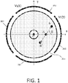
- FIG. 1 is a plan view of an aperture diaphragm 201 with blanking deflector plates 202.
- the deflector plates in the -x-axis and -y-axis can be grounded, so a pair of unipolar blanking voltages (or currents) are applied on the deflector plates 202 in +x-axis and +y-axis.
- the focused electron beam is deflected in the aperture plane from the center 0 to position A in FIG. 1 . Parking a focused electron beam with megawatt power density at the position A of the aperture diaphragm 201 in FIG. 1 can damage and even burn the aperture diaphragm 201 locally.
- the aperture diaphragm 201 may also be shifted laterally due to the tensile stresses resulted from uneven heating and/or temperature distributions.
- the blanking system voltages Vx and Vy can be used to scan the beam from B to B' back and forth at any polar angle ⁇ , but the heat distribution is still rotationally asymmetrical around the aperture.
- the edge rim of the aperture diaphragm 201 can still be shifted, distorted, or damaged.
- JP2005277046 discloses an electron beam blanking device and blanking method.
- US6483117 describes an electronic beam lithography tool providing dimensional stability.
- an electron beam apparatus as recited in claim 1 is provided.
- Embodiments disclosed herein provide a heat-spreading blanking system that addresses the problems stated above with circular, square, or polygonal blanking techniques in an electron beam apparatus. These techniques may be symmetric or may use a symmetric pattern.
- the embodiments disclosed herein provide solutions to the blanking issues resulting from sinking high-power heat onto the aperture diaphragm. Heat sinking on the aperture diaphragm can be spread out instantly and evenly.
- Throughput can be enhanced and resolution of an electron beam apparatus (either a focused electron beam or a shaped electron beam) can be improved.
- the throughput or resolution can be enhanced with increasing beam current or beam energy because the risk of damage to the aperture during blanking is reduced or removed.
- Embodiments disclosed herein can easily be implemented in existing systems.
- FIG. 2 is a cross-sectional diagram of optics in an electron beam apparatus 100 with a blanking system.
- a lens such as a gun lens 102, focuses the electron beam 103 from the emission tip of an electron source 101 toward a crossover around the aperture diaphragm 104.
- the maximum beam current is limited by the beam-limiting aperture 105, and the final beam current to the target (e.g., a semiconductor wafer 106) is further selected by the aperture diaphragm 104 by varying the gun lens 102 focusing strength.
- the condenser lens 107 and objective lens 108 focusing strengths can be optimized to select an optimal numerical aperture (NA) at which the electron beam 103 spot size at the target is minimized for highest resolution.
- NA numerical aperture
- the blanking deflector 109 deflects the electron beam 103 onto the aperture diaphragm 104 when the electron beam should be stopped from reaching the target (e.g., wafer 106).
- wafer generally refers to substrates formed of a semiconductor or non-semiconductor material.
- a semiconductor or non-semiconductor material include, but are not limited to, monocrystalline silicon, gallium nitride, gallium arsenide, indium phosphide, sapphire, and glass.
- substrates may be commonly found and/or processed in semiconductor fabrication facilities.
- a wafer may include one or more layers formed upon a substrate.
- such layers may include, but are not limited to, a photoresist, a dielectric material, a conductive material, and a semiconductive material.
- a photoresist a dielectric material
- a conductive material a conductive material
- a semiconductive material a material that is used in the art.
- wafer as used herein is intended to encompass a wafer including all types of such layers.
- One or more layers formed on a wafer may be patterned or unpatterned.
- a wafer may include a plurality of dies, each having repeatable patterned features or periodic structures. Formation and processing of such layers of material may ultimately result in completed devices.
- Many different types of devices may be formed on a wafer, and the term wafer as used herein is intended to encompass a wafer on which any type of device known in the art is being fabricated.
- the material of the aperture diaphragm 104 may be selected to further reduce the effects of blanking.
- the material in the aperture diaphragm 104 may be burn-resistant, may have a high melting temperature, or may be selected to reduce shifting or distortion.
- the aperture diaphragm 104 includes molybdenum or a molybdenum compound.
- the aperture diaphragm 104 consists of or consists essential of molybdenum or a molybdenum compound.
- the aperture diaphragm 104 can have, for example, an aperture with a diameter from 10 ⁇ m to 100 ⁇ m for a focused electron beam.
- the aperture diaphragm 104 also can have a square aperture with a side length on the scale of, for example, one or more microns for a shaped electron beam.
- FIG. 2 there may be multiple plates in the blanking deflector 109.
- Each plate in the blanking defector 109 is connected to a power supply 110.
- Each plate may have an individual power supply or two or more of the plates may be connected to the same power supply. In an instance, all the plates are connected to the same power supply.
- the electron beam apparatus 100 communicates with a controller 111.
- the controller 111 can communicate with the blanking deflector 109, the power supply 110, or other components of the electron beam apparatus 100.
- the controller 111 can include a processor 112, a storage device 113 in electronic communication with the processor 112, and a communication port 114 in electronic communication with the processor 112. It is to be appreciated that the controller 111 may be implemented in practice by any combination of hardware, software, and firmware. Also, its functions as described herein may be performed by one unit, or divided up among different components, each of which may be implemented in turn by any combination of hardware, software and firmware.
- Program code or instructions for the controller 111 to implement the various methods and functions described herein may be stored in controller readable storage media, such as a memory of the storage device 113, within the controller 111, external to the controller 111, or combinations thereof.
- the controller 111 may be coupled to components of the electron beam apparatus 100 in any suitable manner (e.g., via one or more transmission media, which may include "wired” and/or “wireless” transmission media) such that the controller 111 can receive the output generated by these components of the electron beam apparatus 100.
- the controller 111 can control the pattern of the electron beam 103.
- the controller 111 may perform the steps of FIG. 13 or control the electron beam to have the pattern of FIG. 3 , 5 , 9 , or 11 .
- the controller 111 also may perform other steps or techniques disclosed herein.
- the controller 111, other system(s), or other subsystem(s) described herein may take various forms, including a personal computer system, image computer, mainframe computer system, workstation, network appliance, internet appliance, or other device.
- the term "controller” may be broadly defined to encompass any device having one or more processors, which executes instructions from a memory medium.
- the subsystem(s) or system(s) may also include any suitable processor known in the art such as a parallel processor.
- the subsystem(s) or system(s) may include a platform with high speed processing and software, either as a standalone or a networked tool.
- the different subsystems may be coupled to each other such that images, data, information, instructions, etc. can be sent between the subsystems.
- one subsystem may be coupled to additional subsystem(s) by any suitable transmission media, which may include any suitable wired and/or wireless transmission media known in the art.
- Two or more of such subsystems may also be effectively coupled by a shared computer-readable storage medium (not shown).
- An additional embodiment relates to a non-transitory computer-readable medium storing program instructions executable on a controller for controlling a pattern of the electron beam 103, as disclosed herein.
- storage device 113 or other storage medium may contain non-transitory computer-readable medium that includes program instructions executable on the controller 111.
- the computer-implemented method may include any step(s) of any method(s) described herein.
- the program instructions may be implemented in any of various ways, including procedure-based techniques, component-based techniques, and/or object-oriented techniques, among others.
- the program instructions may be implemented using ActiveX controls, C++ objects, JavaBeans, Microsoft Foundation Classes ("MFC"), SSE (Streaming SIMD Extension) or other technologies or methodologies, as desired.
- MFC Microsoft Foundation Classes
- SSE Streaming SIMD Extension
- Controller 111 may be configured according to any of the embodiments described herein.
- the processor 112 is programmed to perform any of the methods described herein.
- Electron beam 103 energy may be as high as 30 kV and electron beam 103 current may be as high as 100 nA.
- Equation 1 BE is beam energy, BC is beam current, and d is the diameter of the beam spot.
- BE is beam energy
- BC is beam current
- d is the diameter of the beam spot.
- the average power density inside a 150 nm electron beam spot is 17 MW/cm 2 .
- the electron beam 103 crossover size around the aperture in FIG. 2 can be in a range from sub-microns to microns.
- the electron beam 103 may be focused in the aperture plane and scanned over the aperture edge.
- the focused spot size in the aperture plane can be around 0.1 microns or even smaller.
- the power density within the crossover is greater than 20 megawatts per square centimeter.
- the electron beam 103 is kept in motion around the aperture of the aperture diaphragm 104 to spread the heat symmetrically.
- the blanking deflection pattern of the electron beam 103 can be a closed geometrical figure disposed symmetrically around the aperture. A moving locus with a symmetrical pattern may provide the best heat spreading and may be easiest to control, though other pattern configurations are possible. Besides preventing damage to the aperture diaphragm 104, this also may help provide sufficient throughput.
- the blanking process can occur in, for example, 5 ns to 10 ns. During blanking, it may be desired to have less than ten electrons pass through the aperture of the aperture diaphragm 104 from a time when electron beam 103 blanking begins to when the electron beam 103 is blanked. Other speeds and thresholds are possible.
- Damage to the aperture diaphragm may decrease the closer the electron beam is parked to the edge of the aperture bore (i.e., farther away from the aperture). However, this can increase blanking time or blanking voltage. The distance the electron beam is moved from the aperture during blanking, the blanking time, and/or the blanking voltage can be optimized for a particular application.
- FIG. 3 is a plan view of an aperture diaphragm 104 showing a unipolar blanking method with a circular electron locus.
- a circular electron locus for a focused electron beam spreads the heat rotationally symmetric, which is consistent with the aperture shape to avoid the distortion of aperture.
- Use of a circular locus that is rotationally symmetric with a round aperture may reduce temperature differences. Any damage to the aperture diaphragm 104 can be reduced or may be negligible.
- two or more square apertures can used to form a shaped electron beam in a shaped electron beam projection apparatus.
- the power density of a shaped beam for high throughput is in the range of kilowatts per square centimeter over a region of hundreds of microns square.
- the dimensional stability of a square aperture may be important because an aperture shift error can directly result in stitching problems of the exposure patterns in, for instance, an electron beam lithography apparatus.
- the stitching error likely should not be larger than minimum feature sizes around hundreds of nanometers.
- the aperture shift due to the heat tensile stresses by a kilowatt power density electron beam can be as large as submicrons.
- a circular electron locus can be used with a square aperture.
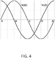
- FIG. 4 shows the blanking voltage signals used in the circular electron locus in FIG. 3 . More precisely the voltages applied on the blanking system deflector plates in FIG. 3 are given in Equations 2, 3, and 4.
- V x t A t cos 2 ⁇ T t
- V y t A t sin 2 ⁇ T t
- a t A m 1 ⁇ exp ⁇ t ⁇
- Vx(t) and Vy(t) are the blanking deflection voltage signals for the x-axis and y-axis deflector plates in FIG. 3 , respectively, and t is the time variable.
- the A m is the peak deflection voltage under which the electron beam is able to be deflected from the center 0 to position A. From the center 0 to position A, the deflection experiences a time (e.g., approximately 3 ⁇ or approximately 30 ns) reflected in the A(t) of Equation 4, if compared to the period T of from 100 ⁇ s to 1,000 ⁇ s
- the time period T in Equations 2 and 3 may be chosen so that the heat on the aperture diaphragm is homogenously distributed rotationally. T may be minimized while providing the desired heat distribution.
- the time constant ⁇ in Equation 4 may be chosen so that the electron beam can be fast deflected and/or blanked from the center 0 to position A. The time constant ⁇ may be minimized while providing the desired deflection/blanking.
- the time constant ⁇ may be on the order of approximately 10 nanoseconds so that only a few electrons can reach toward to the target.
- the time constant ⁇ may be much shorter than the time period T. For example, ⁇ may be 10 ns and T may be 100 ns to 1,000 ⁇ s to blank an electron beam.
- the period T in FIG. 4 may be in an order of millisecond or sub-millisecond (i.e., approximately 1,000 to 10,000 revolutions per second). Selection of the period T allows the heat to spread sufficiently and homogeneously.
- the bore of an aperture 116 may be a square, as shown in FIG. 5 .
- a closed square electron locus during the blanking deflection may be used.
- the electron beam is continuously scanned in a square locus A-B-C-D-E-F-G-H-A, such that the heat dissipation and temperature distribution are rotationally symmetric around the aperture 115.
- the square pattern may match the shape of the aperture 116.
- FIG. 5 shows a unipolar blanking method with a square electron locus and
- FIG. 6 shows the voltage signals applied on the blanking deflector plates for a square electron locus.
- a square electron locus for shaped electron beams to spread heat symmetrically which is consistent with the aperture shape to avoid dimensional errors in stitching patterns of exposures.
- a square electron locus may cause hot spots at or near the corners. However, these hot spots can be managed while reducing damage to the aperture diaphragm. For example, a symmetric pattern can prevent unbalanced heating of the aperture diaphragm 104 even if hot spots are present.
- the distance between the locus and aperture rim can be kept constant.
- the distance is varied rotationally, and the distance is shortest at the corners of the square aperture.
- FIG. 7 shows a schematic block diagram of exemplary functional elements to control unipolar blanking with a circular electron locus.
- the elements include four digital-to-analog converters (DAC) 402-405 that control four power supply modules 406-409.
- the field-programmable gate array (FPGA) 401 can generate DAC data at a rate sufficient to define slow sine waves.
- the FPGA 401 can generated DAC data to define, for example, four quadrature sine waves.
- the DAC 402-405 each can produce control voltages of 0 volts to +10 volts.
- Output voltages Phase 1 through Phase 4 can be, for example, 0 volts to +200 volts. An arbitrary voltage level of +200 volts may be chosen as required.
- a similar system can be used with a square electron pattern or electron patterns with other shapes.
- FIG. 8 is a diagram showing blanking system-driving electronics.
- the electronics include a four channel switching driver.
- Four gate drivers 501-504, which may be opto-coupled, are connected to four gates 505-508.
- the gates 505-508 are connected to the plates in the deflector 109.
- Each plate in the deflector 109 may be connected to a separate gate.
- the low output level may always be at ground (e.g., 0 volts).
- All outputs in the plates of the deflector 109 can switch simultaneously with fastest possible slewing.
- the outputs may be slow sine waves and can be DAC controlled power supplies.
- the outputs can be at 0, 90, 180, 270 degrees phase relationship.
- the unblank signal may toggle at any time and unblank is a logic level control signal. The outputs may pause when unblanked, and resume the slow sine waves when blanked.
- a closed two-dimensional polygonal locus can spread the heat evenly around the aperture 115.
- the circular electron locus may be a specific polygonal shape by considering the number of the polygon sides to be infinite. Polygons with 4, 6, 8, 12, 16, or more sides are possible.
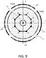
- the electron beam is continuously scanned in a polygonal locus A-B-C-D-E-F-G-H-I-A, such that the heat dissipation and temperature distribution are rotationally symmetric around the aperture 115.
- FIG. 9 and FIG. 10 show a unipolar blanking method with an octagonal locus, from which one may find that both the electron locus and the voltage signal waveforms are close to circular blanking properties when the number of the polygon sides are relatively large.
- a polygonal electron locus typically an octagonal locus, spreads the heat on the aperture diaphragm in any combination of electron beams.
- a polygonal electron locus may cause hot spots at or near the corners. However, these hot spots can be managed while reducing damage to the aperture diaphragm. For example, a symmetric pattern can prevent unbalanced heating of the aperture diaphragm 104 even if hot spots are present.
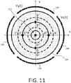
- a locus-variable blanking method as used in the present invention is performed. This is illustrated in FIG. 11 .
- locus-variable blanking two square-waveform signals with a time period approximately twice as large as the Vx(t) and Vy(t) time period T in FIG. 4 can be superimposed together.
- the electron locus goes in a periodic manner of ABCDA, A'B'C'D'A', ABCDA, A"B"C"D"A", ABCDA.
- A"B"C"D"A" is between ABCDA and the aperture 115.
- A'B'C'D'A' is farther from the aperture 115 than either ABCDA or A"B"C"D"A". Additional patterns at various distances from the aperture 115 besides ABCDA, A'B'C'D'A', and A"B"C"D"A" are possible.
- a locus-variable blanking method spreads the heat in wider regions consistent with the concept that the electron power-sinking heat is fundamentally dissipated in a narrowly-distributed ring even though a closed electron locus is applied in blanking and over-heating risks remain local.
- locus-variable method can be used with other shapes not forming part of the claimed invention, such as square or polygonal.
- the crossover spot size in the aperture plane may be small in a focused electron beam apparatus in FIG. 2 . So the high density power can be dissipated in a narrow region of the aperture diaphragm, as shown in FIG. 12 .
- the electron beam power-heat transformation is modeled and simulated in FIG. 12 .
- the electron beam sinking temperature T is mainly distributed in a narrow region within 2a or 4a ("a" is the crossover spot radius in sub-microns). Even if the electron beam is blanked in a way of circular locus (or square locus), the heat is still distributed in a narrowly circular (or square) ring.
- the saturated temperature drops greater than 75%.
- the gap distance between the locus A" and A, or between the locus A and A' may be at least greater than 10a. If the blanked electron beam is focused with high power density, the spot radius is, for example, 75 nm, so the gap distance can be set larger to greater than 100a (i.e., greater than 7.5 ⁇ m). The gap distance may be configured to avoid high deflection voltages in some embodiments.
- the pattern of the electron beam during blanking is not limited to circular, square, or polygonal.
- mathematical roulette curves e.g., hypotrochoids, epitrochoids, cycloids, epicycloids, hypocycloids, or trochoids
- FIG. 13 is a flowchart of an electron beam blanking embodiment.
- An electron beam is directed 300 through an aperture.
- At least one plate in a deflector is biased 301.
- the electron beam is deflected 302 so that the electron beam is directed at an aperture diaphragm in a pattern.
- the pattern can be around an entirety of the aperture.
- the pattern is a circle.
- the pattern also has a variable locus relative to the aperture.
- the methods may also include any other step(s) that can be performed by the electron beam apparatus subsystem and/or computer subsystem(s) or system(s) described herein.
- the steps are performed by one or more computer systems, which may be configured according to any of the embodiments described herein.
- the methods described above may be performed by any of the system embodiments described herein.
Landscapes
- Analytical Chemistry (AREA)
- Chemical & Material Sciences (AREA)
- Physics & Mathematics (AREA)
- General Physics & Mathematics (AREA)
- Engineering & Computer Science (AREA)
- Environmental & Geological Engineering (AREA)
- Health & Medical Sciences (AREA)
- Epidemiology (AREA)
- Public Health (AREA)
- Electron Beam Exposure (AREA)
- Manufacturing & Machinery (AREA)
- Powder Metallurgy (AREA)
- Extrusion Of Metal (AREA)
Claims (9)
- Elektronenstrahlvorrichtung (100), umfassend:eine Aperturblende (104), die eine Apertur definiert, durch die ein Elektronenstrahl projiziert wird;eine Linse (102), die dazu konfiguriert ist, den Elektronenstrahl in Richtung der Apertur (115) zu fokussieren;einen Deflektor (109), der dazu konfiguriert ist, den Elektronenstrahl an der Aperturblende abzulenken, wobei der Deflektor eine Vielzahl von Platten beinhaltet;eine Vielzahl von Leistungsversorgungsmodulen (110), wobei die Leistungsversorgungsmodule dazu konfiguriert sind, die Platten so vorzuspannen, dass der Elektronenstrahl an der Aperturblende in einem Muster um eine Gesamtheit der Apertur herum gelenkt wird;eine Steuerung (111), die programmiert ist, um eine Vorspannung zu mindestens einer der Platten zu steuern, wodurch der Elektronenstrahl an der Aperturblende in einem Muster um eine Gesamtheit der Apertur herum gelenkt wird;wobei die Steuerung ferner programmiert ist, um den Elektronenstrahl so zu lenken, dass das Muster eine variable Ortskurve relativ zu der Apertur aufweist; undwobei die variable Ortskurve das Muster umfasst, das periodisch zwischen drei Ortskurven umschaltet, wobei jede Ortskurve eine kreisförmige Form aufweist und die drei Ortskurven konzentrisch um die Apertur herum angeordnet sind, wobei das Muster periodisch von einer ersten kreisförmigen Ortskurve (ABCDA) zu einer zweiten kreisförmigen Ortskurve (A'B'C'D'A'), die weiter von der Apertur entfernt ist als die erste kreisförmige Ortskurve, dann zu einer dritten kreisförmigen Ortskurve (A"B"C"D"A") zwischen der Apertur und der ersten kreisförmigen Ortskurve und zurück zur ersten Ortskurve umgeschaltet wird.
- Elektronenstrahlvorrichtung nach Anspruch 1, wobei der Deflektor (109) vier der Platten beinhaltet und die Elektronenstrahlvorrichtung vier der Leistungsversorgungsmodule (110) beinhaltet.
- Elektronenstrahlvorrichtung nach Anspruch 1, wobei der Deflektor (109) mindestens acht der Platten beinhaltet.
- Elektronenstrahlvorrichtung nach Anspruch 1, ferner umfassend ein Gestell, das dazu konfiguriert ist, einen Wafer in einem Pfad des Elektronenstrahls zu halten.
- Elektronenstrahlvorrichtung nach Anspruch 1, wobei ein Fokus des Elektronenstrahls von einer Mitte der Apertur entfernt ist.
- Elektronenstrahlvorrichtung nach Anspruch 1, wobei die Linse (102) eine Kathodenlinse ist und wobei die Elektronenstrahlvorrichtung ferner Folgendes umfasst:eine Platte, die eine Strahlbegrenzungsapertur definiert;eine Kondensorlinse (107); undeine Objektivlinse (108).
- Elektronenstrahlvorrichtung nach Anspruch 1, wobei die Leistungsversorgungsmodule (110) dazu konfiguriert sind, die Platten so vorzuspannen, dass der Elektronenstrahl auf die Aperturblende (104) gelenkt wird und um die Apertur herum kontinuierlich abgetastet wird.
- Elektronenstrahlvorrichtung nach Anspruch 1, wobei die Steuerung (111) ferner programmiert ist, um die Spannung der Leistungsversorgungsmodule (110) zu steuern, um mindestens eine der Platten vorzuspannen.
- Verfahren, umfassend:Lenken eines Elektronenstrahls durch eine Apertur (300), wobei die Apertur durch eine Aperturblende definiert ist und wobei ein Deflektor, der eine Vielzahl von Platten beinhaltet, um die Aperturblende herum angeordnet ist;Vorspannen mindestens einer der Platten in dem Deflektor (301) ;Ablenken des Elektronenstrahls unter Verwendung des Deflektors, sodass der Elektronenstrahl an der Aperturblende in einem Muster um eine Gesamtheit der Apertur (302) herum gelenkt wird;wobei das Muster eine variable Ortskurve relativ zu der Apertur aufweist; undwobei die variable Ortskurve das Muster umfasst, das periodisch zwischen drei Ortskurven umschaltet, wobei jede Ortskurve eine kreisförmige Form aufweist und die drei Ortskurven konzentrisch um die Apertur herum angeordnet sind, wobei das Muster periodisch von einer ersten kreisförmigen Ortskurve (ABCDA) zu einer zweiten kreisförmigen Ortskurve (A'B'C'D'A'), die weiter von der Apertur entfernt ist als die erste kreisförmige Ortskurve, dann zu einer dritten kreisförmigen Ortskurve (A"B"C"D"A") zwischen der Apertur und der ersten kreisförmigen Ortskurve und zurück zur ersten Ortskurve umgeschaltet wird.
Applications Claiming Priority (3)
| Application Number | Priority Date | Filing Date | Title |
|---|---|---|---|
| US201662276824P | 2016-01-09 | 2016-01-09 | |
| US15/255,314 US9881764B2 (en) | 2016-01-09 | 2016-09-02 | Heat-spreading blanking system for high throughput electron beam apparatus |
| PCT/US2017/012386 WO2017120373A1 (en) | 2016-01-09 | 2017-01-05 | Heat-spreadable blanking system for high throughput electron beam apparatus |
Publications (3)
| Publication Number | Publication Date |
|---|---|
| EP3400608A1 EP3400608A1 (de) | 2018-11-14 |
| EP3400608A4 EP3400608A4 (de) | 2019-08-21 |
| EP3400608B1 true EP3400608B1 (de) | 2022-12-28 |
Family
ID=59273928
Family Applications (1)
| Application Number | Title | Priority Date | Filing Date |
|---|---|---|---|
| EP17736363.7A Active EP3400608B1 (de) | 2016-01-09 | 2017-01-05 | Elektronenstrahlvorrichtung umfassend ein austastsystem mit verbesserter wärmeverteilung |
Country Status (9)
| Country | Link |
|---|---|
| US (1) | US9881764B2 (de) |
| EP (1) | EP3400608B1 (de) |
| JP (2) | JP2019503051A (de) |
| KR (1) | KR102468977B1 (de) |
| CN (2) | CN108431939A (de) |
| IL (1) | IL259967B (de) |
| SG (1) | SG11201804756RA (de) |
| TW (1) | TWI707376B (de) |
| WO (1) | WO2017120373A1 (de) |
Families Citing this family (2)
| Publication number | Priority date | Publication date | Assignee | Title |
|---|---|---|---|---|
| US12100574B2 (en) * | 2020-07-01 | 2024-09-24 | Kla Corporation | Target and algorithm to measure overlay by modeling back scattering electrons on overlapping structures |
| CN116300335B (zh) * | 2023-02-28 | 2025-10-10 | 中国电子科技集团公司第十三研究所 | 一种电子束光阑和束闸一体化装置和电子光学系统 |
Family Cites Families (30)
| Publication number | Priority date | Publication date | Assignee | Title |
|---|---|---|---|---|
| US4199689A (en) * | 1977-12-21 | 1980-04-22 | Tokyo Shibaura Denki Kabushiki Kaisha | Electron beam exposing method and electron beam apparatus |
| JPS59201416A (ja) * | 1983-04-28 | 1984-11-15 | Jeol Ltd | 荷電粒子線ブランキング装置 |
| JPS60130040A (ja) * | 1983-12-16 | 1985-07-11 | Toshiba Mach Co Ltd | 荷電ビ−ム光学鏡筒 |
| JPS62170139A (ja) | 1986-01-22 | 1987-07-27 | Fujitsu Ltd | 電子ビ−ム・ブランキング装置 |
| JPS62180946A (ja) * | 1986-02-01 | 1987-08-08 | Fujitsu Ltd | 電子ビ−ム・パルスゲ−ト |
| US6278124B1 (en) * | 1998-03-05 | 2001-08-21 | Dupont Photomasks, Inc | Electron beam blanking method and system for electron beam lithographic processing |
| JP2000251815A (ja) | 1999-03-03 | 2000-09-14 | Nikon Corp | ブランキング装置 |
| US6483117B1 (en) | 1999-06-16 | 2002-11-19 | Nikon Corporation | Symmetric blanking for high stability in electron beam exposure systems |
| US6521896B1 (en) | 2000-06-01 | 2003-02-18 | Applied Materials, Inc. | Blanker assembly employing dielectric material |
| JP2001345258A (ja) | 2000-06-02 | 2001-12-14 | A & D Co Ltd | 電子ビーム装置 |
| TWI288424B (en) * | 2000-06-27 | 2007-10-11 | Ebara Corp | Inspection apparatus and inspection method |
| EP1339100A1 (de) | 2000-12-01 | 2003-08-27 | Ebara Corporation | Untersuchungsverfahren und -vorrichtung mit elektronenstrahl und diese benutzendes bauelementeherstellungsverfahren |
| JP2002217088A (ja) | 2001-01-17 | 2002-08-02 | Nikon Corp | 荷電粒子線露光装置、荷電粒子線露光方法及び半導体デバイスの製造方法 |
| KR20050072101A (ko) * | 2002-10-28 | 2005-07-08 | 마츠시타 덴끼 산교 가부시키가이샤 | 전자선 노광 방법 및 전자선 노광 장치 |
| JP2005032837A (ja) * | 2003-07-08 | 2005-02-03 | Canon Inc | 荷電粒子描画方法及び該方法を用いたデバイス製造方法 |
| JP4015626B2 (ja) * | 2004-01-14 | 2007-11-28 | 株式会社日立ハイテクノロジーズ | 荷電粒子ビーム露光装置 |
| JP2005277046A (ja) | 2004-03-24 | 2005-10-06 | Tokyo Seimitsu Co Ltd | 電子ビームのブランキング装置及びブランキング方法 |
| GB2414857B (en) | 2004-06-03 | 2009-02-25 | Nanobeam Ltd | Apparatus for blanking a charged particle beam |
| JP2006005133A (ja) | 2004-06-17 | 2006-01-05 | Hitachi High-Technologies Corp | 電子線描画装置 |
| JP5222142B2 (ja) * | 2005-09-06 | 2013-06-26 | カール・ツァイス・エスエムティー・ゲーエムベーハー | 粒子光学部品 |
| JP5273495B2 (ja) * | 2005-12-13 | 2013-08-28 | 独立行政法人産業技術総合研究所 | クラスター成膜装置及び成膜方法、並びにクラスター生成装置及び生成方法 |
| JP4795890B2 (ja) | 2006-08-09 | 2011-10-19 | 富士通株式会社 | 伝送線路型ブランキング装置及び電子ビーム露光装置 |
| KR101481950B1 (ko) * | 2008-02-26 | 2015-01-14 | 마퍼 리쏘그라피 아이피 비.브이. | 투사 렌즈 배열체 |
| JP5484808B2 (ja) * | 2008-09-19 | 2014-05-07 | 株式会社ニューフレアテクノロジー | 描画装置及び描画方法 |
| DE102008062450B4 (de) | 2008-12-13 | 2012-05-03 | Vistec Electron Beam Gmbh | Anordnung zur Beleuchtung eines Substrats mit mehreren individuell geformten Partikelstrahlen zur hochauflösenden Lithographie von Strukturmustern |
| EP2492950B1 (de) | 2011-02-25 | 2018-04-11 | FEI Company | Verfahren zum schnellen Schalten zwischen einem Hochstrommodus und einem Niederstrommodus in einem System mit geladenem Teilchenstrahl |
| JP5970213B2 (ja) * | 2012-03-19 | 2016-08-17 | 株式会社ニューフレアテクノロジー | マルチ荷電粒子ビーム描画装置及びマルチ荷電粒子ビーム描画方法 |
| JP5851352B2 (ja) | 2012-06-15 | 2016-02-03 | 株式会社日立ハイテクノロジーズ | 荷電粒子線装置 |
| US9269542B2 (en) * | 2013-11-01 | 2016-02-23 | Varian Semiconductor Equipment Associates, Inc. | Plasma cathode charged particle lithography system |
| JP6215061B2 (ja) * | 2014-01-14 | 2017-10-18 | 株式会社アドバンテスト | 電子ビーム露光装置 |
-
2016
- 2016-09-02 US US15/255,314 patent/US9881764B2/en active Active
-
2017
- 2017-01-05 SG SG11201804756RA patent/SG11201804756RA/en unknown
- 2017-01-05 EP EP17736363.7A patent/EP3400608B1/de active Active
- 2017-01-05 CN CN201780005788.7A patent/CN108431939A/zh active Pending
- 2017-01-05 JP JP2018535303A patent/JP2019503051A/ja active Pending
- 2017-01-05 CN CN202111286513.XA patent/CN113990728B/zh active Active
- 2017-01-05 WO PCT/US2017/012386 patent/WO2017120373A1/en not_active Ceased
- 2017-01-05 KR KR1020187022825A patent/KR102468977B1/ko active Active
- 2017-01-09 TW TW106100564A patent/TWI707376B/zh active
-
2018
- 2018-06-12 IL IL259967A patent/IL259967B/en unknown
-
2021
- 2021-09-24 JP JP2021155115A patent/JP7216784B2/ja active Active
Also Published As
| Publication number | Publication date |
|---|---|
| EP3400608A1 (de) | 2018-11-14 |
| JP2019503051A (ja) | 2019-01-31 |
| US9881764B2 (en) | 2018-01-30 |
| TW201735087A (zh) | 2017-10-01 |
| CN108431939A (zh) | 2018-08-21 |
| IL259967B (en) | 2022-04-01 |
| CN113990728B (zh) | 2024-03-26 |
| EP3400608A4 (de) | 2019-08-21 |
| KR102468977B1 (ko) | 2022-11-18 |
| SG11201804756RA (en) | 2018-07-30 |
| US20170200581A1 (en) | 2017-07-13 |
| JP7216784B2 (ja) | 2023-02-01 |
| TWI707376B (zh) | 2020-10-11 |
| WO2017120373A1 (en) | 2017-07-13 |
| KR20180093098A (ko) | 2018-08-20 |
| IL259967A (en) | 2018-07-31 |
| JP2021193682A (ja) | 2021-12-23 |
| CN113990728A (zh) | 2022-01-28 |
Similar Documents
| Publication | Publication Date | Title |
|---|---|---|
| JP5053514B2 (ja) | 電子ビーム露光システム | |
| US6433348B1 (en) | Lithography using multiple pass raster-shaped beam | |
| JP6013089B2 (ja) | 荷電粒子ビーム描画方法及び荷電粒子ビーム描画装置 | |
| US11145489B2 (en) | Multi-charged-particle beam writing apparatus and multi-charged-particle beam writing method | |
| US10503083B2 (en) | Apparatus and method for using scanning light beam for film or surface modification | |
| JP2000208085A (ja) | 低電圧粒子ビ―ムを用いた半導体検査用の電圧コントラスト方法及び装置 | |
| US20180284620A1 (en) | Electron beam irradiation apparatus and electron beam dynamic focus adjustment method | |
| US8759797B2 (en) | Drawing apparatus, drawing method, and method of manufacturing article | |
| US9697981B2 (en) | Blanking system for multi charged particle beams, and multi charged particle beam writing apparatus | |
| JP7216784B2 (ja) | 電子ビーム装置 | |
| JP2015211175A (ja) | リソグラフィ装置、および物品の製造方法 | |
| US9607807B2 (en) | Charged particle beam exposure apparatus suitable for drawing on line patterns, and exposure method using the same | |
| JP4267739B2 (ja) | 電子ビームリソグラフィ処理のための電子ビームブランキング方法およびシステム | |
| US6483117B1 (en) | Symmetric blanking for high stability in electron beam exposure systems | |
| TWI771649B (zh) | 控制帶電粒子束之能量分散之設備及方法 | |
| US20250253121A1 (en) | Systems and methods of sem inspection using selective scan approach | |
| KR20160002360A (ko) | 리소그래피 장치 및 물품의 제조 방법 | |
| JP2015207608A (ja) | リソグラフィ装置、および物品の製造方法 | |
| US20260045440A1 (en) | Creation of electron beams using a micro-deflector array | |
| JPH01278725A (ja) | 荷電粒子ビーム露光装置 | |
| JP2005032838A (ja) | 荷電粒子線描画方法および装置ならびにデバイス製造方法 |
Legal Events
| Date | Code | Title | Description |
|---|---|---|---|
| STAA | Information on the status of an ep patent application or granted ep patent |
Free format text: STATUS: THE INTERNATIONAL PUBLICATION HAS BEEN MADE |
|
| PUAI | Public reference made under article 153(3) epc to a published international application that has entered the european phase |
Free format text: ORIGINAL CODE: 0009012 |
|
| STAA | Information on the status of an ep patent application or granted ep patent |
Free format text: STATUS: REQUEST FOR EXAMINATION WAS MADE |
|
| 17P | Request for examination filed |
Effective date: 20180720 |
|
| AK | Designated contracting states |
Kind code of ref document: A1 Designated state(s): AL AT BE BG CH CY CZ DE DK EE ES FI FR GB GR HR HU IE IS IT LI LT LU LV MC MK MT NL NO PL PT RO RS SE SI SK SM TR |
|
| AX | Request for extension of the european patent |
Extension state: BA ME |
|
| DAV | Request for validation of the european patent (deleted) | ||
| DAX | Request for extension of the european patent (deleted) | ||
| REG | Reference to a national code |
Ref country code: DE Ref legal event code: R079 Ref document number: 602017065014 Country of ref document: DE Free format text: PREVIOUS MAIN CLASS: H01L0021660000 Ipc: H01J0037147000 |
|
| A4 | Supplementary search report drawn up and despatched |
Effective date: 20190723 |
|
| RIC1 | Information provided on ipc code assigned before grant |
Ipc: H01J 37/04 20060101ALI20190717BHEP Ipc: H01J 37/147 20060101AFI20190717BHEP |
|
| STAA | Information on the status of an ep patent application or granted ep patent |
Free format text: STATUS: EXAMINATION IS IN PROGRESS |
|
| 17Q | First examination report despatched |
Effective date: 20200609 |
|
| GRAP | Despatch of communication of intention to grant a patent |
Free format text: ORIGINAL CODE: EPIDOSNIGR1 |
|
| STAA | Information on the status of an ep patent application or granted ep patent |
Free format text: STATUS: GRANT OF PATENT IS INTENDED |
|
| INTG | Intention to grant announced |
Effective date: 20220712 |
|
| GRAS | Grant fee paid |
Free format text: ORIGINAL CODE: EPIDOSNIGR3 |
|
| GRAA | (expected) grant |
Free format text: ORIGINAL CODE: 0009210 |
|
| STAA | Information on the status of an ep patent application or granted ep patent |
Free format text: STATUS: THE PATENT HAS BEEN GRANTED |
|
| AK | Designated contracting states |
Kind code of ref document: B1 Designated state(s): AL AT BE BG CH CY CZ DE DK EE ES FI FR GB GR HR HU IE IS IT LI LT LU LV MC MK MT NL NO PL PT RO RS SE SI SK SM TR |
|
| REG | Reference to a national code |
Ref country code: GB Ref legal event code: FG4D |
|
| REG | Reference to a national code |
Ref country code: CH Ref legal event code: EP |
|
| REG | Reference to a national code |
Ref country code: DE Ref legal event code: R096 Ref document number: 602017065014 Country of ref document: DE |
|
| REG | Reference to a national code |
Ref country code: AT Ref legal event code: REF Ref document number: 1541003 Country of ref document: AT Kind code of ref document: T Effective date: 20230115 |
|
| REG | Reference to a national code |
Ref country code: NL Ref legal event code: FP Ref country code: IE Ref legal event code: FG4D |
|
| REG | Reference to a national code |
Ref country code: LT Ref legal event code: MG9D |
|
| PG25 | Lapsed in a contracting state [announced via postgrant information from national office to epo] |
Ref country code: SE Free format text: LAPSE BECAUSE OF FAILURE TO SUBMIT A TRANSLATION OF THE DESCRIPTION OR TO PAY THE FEE WITHIN THE PRESCRIBED TIME-LIMIT Effective date: 20221228 Ref country code: NO Free format text: LAPSE BECAUSE OF FAILURE TO SUBMIT A TRANSLATION OF THE DESCRIPTION OR TO PAY THE FEE WITHIN THE PRESCRIBED TIME-LIMIT Effective date: 20230328 Ref country code: LT Free format text: LAPSE BECAUSE OF FAILURE TO SUBMIT A TRANSLATION OF THE DESCRIPTION OR TO PAY THE FEE WITHIN THE PRESCRIBED TIME-LIMIT Effective date: 20221228 Ref country code: FI Free format text: LAPSE BECAUSE OF FAILURE TO SUBMIT A TRANSLATION OF THE DESCRIPTION OR TO PAY THE FEE WITHIN THE PRESCRIBED TIME-LIMIT Effective date: 20221228 |
|
| REG | Reference to a national code |
Ref country code: AT Ref legal event code: MK05 Ref document number: 1541003 Country of ref document: AT Kind code of ref document: T Effective date: 20221228 |
|
| PG25 | Lapsed in a contracting state [announced via postgrant information from national office to epo] |
Ref country code: RS Free format text: LAPSE BECAUSE OF FAILURE TO SUBMIT A TRANSLATION OF THE DESCRIPTION OR TO PAY THE FEE WITHIN THE PRESCRIBED TIME-LIMIT Effective date: 20221228 Ref country code: LV Free format text: LAPSE BECAUSE OF FAILURE TO SUBMIT A TRANSLATION OF THE DESCRIPTION OR TO PAY THE FEE WITHIN THE PRESCRIBED TIME-LIMIT Effective date: 20221228 Ref country code: HR Free format text: LAPSE BECAUSE OF FAILURE TO SUBMIT A TRANSLATION OF THE DESCRIPTION OR TO PAY THE FEE WITHIN THE PRESCRIBED TIME-LIMIT Effective date: 20221228 Ref country code: GR Free format text: LAPSE BECAUSE OF FAILURE TO SUBMIT A TRANSLATION OF THE DESCRIPTION OR TO PAY THE FEE WITHIN THE PRESCRIBED TIME-LIMIT Effective date: 20230329 |
|
| P01 | Opt-out of the competence of the unified patent court (upc) registered |
Effective date: 20230525 |
|
| PG25 | Lapsed in a contracting state [announced via postgrant information from national office to epo] |
Ref country code: SM Free format text: LAPSE BECAUSE OF FAILURE TO SUBMIT A TRANSLATION OF THE DESCRIPTION OR TO PAY THE FEE WITHIN THE PRESCRIBED TIME-LIMIT Effective date: 20221228 Ref country code: RO Free format text: LAPSE BECAUSE OF FAILURE TO SUBMIT A TRANSLATION OF THE DESCRIPTION OR TO PAY THE FEE WITHIN THE PRESCRIBED TIME-LIMIT Effective date: 20221228 Ref country code: PT Free format text: LAPSE BECAUSE OF FAILURE TO SUBMIT A TRANSLATION OF THE DESCRIPTION OR TO PAY THE FEE WITHIN THE PRESCRIBED TIME-LIMIT Effective date: 20230428 Ref country code: ES Free format text: LAPSE BECAUSE OF FAILURE TO SUBMIT A TRANSLATION OF THE DESCRIPTION OR TO PAY THE FEE WITHIN THE PRESCRIBED TIME-LIMIT Effective date: 20221228 Ref country code: EE Free format text: LAPSE BECAUSE OF FAILURE TO SUBMIT A TRANSLATION OF THE DESCRIPTION OR TO PAY THE FEE WITHIN THE PRESCRIBED TIME-LIMIT Effective date: 20221228 Ref country code: CZ Free format text: LAPSE BECAUSE OF FAILURE TO SUBMIT A TRANSLATION OF THE DESCRIPTION OR TO PAY THE FEE WITHIN THE PRESCRIBED TIME-LIMIT Effective date: 20221228 Ref country code: AT Free format text: LAPSE BECAUSE OF FAILURE TO SUBMIT A TRANSLATION OF THE DESCRIPTION OR TO PAY THE FEE WITHIN THE PRESCRIBED TIME-LIMIT Effective date: 20221228 |
|
| PG25 | Lapsed in a contracting state [announced via postgrant information from national office to epo] |
Ref country code: SK Free format text: LAPSE BECAUSE OF FAILURE TO SUBMIT A TRANSLATION OF THE DESCRIPTION OR TO PAY THE FEE WITHIN THE PRESCRIBED TIME-LIMIT Effective date: 20221228 Ref country code: PL Free format text: LAPSE BECAUSE OF FAILURE TO SUBMIT A TRANSLATION OF THE DESCRIPTION OR TO PAY THE FEE WITHIN THE PRESCRIBED TIME-LIMIT Effective date: 20221228 Ref country code: IS Free format text: LAPSE BECAUSE OF FAILURE TO SUBMIT A TRANSLATION OF THE DESCRIPTION OR TO PAY THE FEE WITHIN THE PRESCRIBED TIME-LIMIT Effective date: 20230428 Ref country code: AL Free format text: LAPSE BECAUSE OF FAILURE TO SUBMIT A TRANSLATION OF THE DESCRIPTION OR TO PAY THE FEE WITHIN THE PRESCRIBED TIME-LIMIT Effective date: 20221228 |
|
| REG | Reference to a national code |
Ref country code: CH Ref legal event code: PL |
|
| PG25 | Lapsed in a contracting state [announced via postgrant information from national office to epo] |
Ref country code: MC Free format text: LAPSE BECAUSE OF FAILURE TO SUBMIT A TRANSLATION OF THE DESCRIPTION OR TO PAY THE FEE WITHIN THE PRESCRIBED TIME-LIMIT Effective date: 20221228 Ref country code: LU Free format text: LAPSE BECAUSE OF NON-PAYMENT OF DUE FEES Effective date: 20230105 |
|
| REG | Reference to a national code |
Ref country code: DE Ref legal event code: R097 Ref document number: 602017065014 Country of ref document: DE |
|
| REG | Reference to a national code |
Ref country code: BE Ref legal event code: MM Effective date: 20230131 |
|
| PG25 | Lapsed in a contracting state [announced via postgrant information from national office to epo] |
Ref country code: LI Free format text: LAPSE BECAUSE OF NON-PAYMENT OF DUE FEES Effective date: 20230131 Ref country code: DK Free format text: LAPSE BECAUSE OF FAILURE TO SUBMIT A TRANSLATION OF THE DESCRIPTION OR TO PAY THE FEE WITHIN THE PRESCRIBED TIME-LIMIT Effective date: 20221228 Ref country code: CH Free format text: LAPSE BECAUSE OF NON-PAYMENT OF DUE FEES Effective date: 20230131 |
|
| PLBE | No opposition filed within time limit |
Free format text: ORIGINAL CODE: 0009261 |
|
| STAA | Information on the status of an ep patent application or granted ep patent |
Free format text: STATUS: NO OPPOSITION FILED WITHIN TIME LIMIT |
|
| GBPC | Gb: european patent ceased through non-payment of renewal fee |
Effective date: 20230328 |
|
| PG25 | Lapsed in a contracting state [announced via postgrant information from national office to epo] |
Ref country code: BE Free format text: LAPSE BECAUSE OF NON-PAYMENT OF DUE FEES Effective date: 20230131 |
|
| 26N | No opposition filed |
Effective date: 20230929 |
|
| PG25 | Lapsed in a contracting state [announced via postgrant information from national office to epo] |
Ref country code: GB Free format text: LAPSE BECAUSE OF NON-PAYMENT OF DUE FEES Effective date: 20230328 |
|
| PG25 | Lapsed in a contracting state [announced via postgrant information from national office to epo] |
Ref country code: SI Free format text: LAPSE BECAUSE OF FAILURE TO SUBMIT A TRANSLATION OF THE DESCRIPTION OR TO PAY THE FEE WITHIN THE PRESCRIBED TIME-LIMIT Effective date: 20221228 Ref country code: IE Free format text: LAPSE BECAUSE OF NON-PAYMENT OF DUE FEES Effective date: 20230105 Ref country code: GB Free format text: LAPSE BECAUSE OF NON-PAYMENT OF DUE FEES Effective date: 20230328 Ref country code: FR Free format text: LAPSE BECAUSE OF NON-PAYMENT OF DUE FEES Effective date: 20230228 |
|
| PG25 | Lapsed in a contracting state [announced via postgrant information from national office to epo] |
Ref country code: IT Free format text: LAPSE BECAUSE OF FAILURE TO SUBMIT A TRANSLATION OF THE DESCRIPTION OR TO PAY THE FEE WITHIN THE PRESCRIBED TIME-LIMIT Effective date: 20221228 |
|
| PG25 | Lapsed in a contracting state [announced via postgrant information from national office to epo] |
Ref country code: BG Free format text: LAPSE BECAUSE OF FAILURE TO SUBMIT A TRANSLATION OF THE DESCRIPTION OR TO PAY THE FEE WITHIN THE PRESCRIBED TIME-LIMIT Effective date: 20221228 |
|
| PG25 | Lapsed in a contracting state [announced via postgrant information from national office to epo] |
Ref country code: BG Free format text: LAPSE BECAUSE OF FAILURE TO SUBMIT A TRANSLATION OF THE DESCRIPTION OR TO PAY THE FEE WITHIN THE PRESCRIBED TIME-LIMIT Effective date: 20221228 |
|
| PG25 | Lapsed in a contracting state [announced via postgrant information from national office to epo] |
Ref country code: CY Free format text: LAPSE BECAUSE OF FAILURE TO SUBMIT A TRANSLATION OF THE DESCRIPTION OR TO PAY THE FEE WITHIN THE PRESCRIBED TIME-LIMIT; INVALID AB INITIO Effective date: 20170105 |
|
| PG25 | Lapsed in a contracting state [announced via postgrant information from national office to epo] |
Ref country code: HU Free format text: LAPSE BECAUSE OF FAILURE TO SUBMIT A TRANSLATION OF THE DESCRIPTION OR TO PAY THE FEE WITHIN THE PRESCRIBED TIME-LIMIT; INVALID AB INITIO Effective date: 20170105 |
|
| PG25 | Lapsed in a contracting state [announced via postgrant information from national office to epo] |
Ref country code: TR Free format text: LAPSE BECAUSE OF FAILURE TO SUBMIT A TRANSLATION OF THE DESCRIPTION OR TO PAY THE FEE WITHIN THE PRESCRIBED TIME-LIMIT Effective date: 20221228 |
|
| PGFP | Annual fee paid to national office [announced via postgrant information from national office to epo] |
Ref country code: NL Payment date: 20260126 Year of fee payment: 10 |
|
| PGFP | Annual fee paid to national office [announced via postgrant information from national office to epo] |
Ref country code: DE Payment date: 20260128 Year of fee payment: 10 |