EP3396232B1 - Lichtemittierendes element und beleuchtungsvorrichtung - Google Patents
Lichtemittierendes element und beleuchtungsvorrichtung Download PDFInfo
- Publication number
- EP3396232B1 EP3396232B1 EP16877936.1A EP16877936A EP3396232B1 EP 3396232 B1 EP3396232 B1 EP 3396232B1 EP 16877936 A EP16877936 A EP 16877936A EP 3396232 B1 EP3396232 B1 EP 3396232B1
- Authority
- EP
- European Patent Office
- Prior art keywords
- layer
- light
- phosphor
- substrate
- emitting element
- Prior art date
- Legal status (The legal status is an assumption and is not a legal conclusion. Google has not performed a legal analysis and makes no representation as to the accuracy of the status listed.)
- Active
Links
Images


Classifications
-
- G—PHYSICS
- G02—OPTICS
- G02B—OPTICAL ELEMENTS, SYSTEMS OR APPARATUS
- G02B5/00—Optical elements other than lenses
- G02B5/02—Diffusing elements; Afocal elements
- G02B5/0205—Diffusing elements; Afocal elements characterised by the diffusing properties
- G02B5/0236—Diffusing elements; Afocal elements characterised by the diffusing properties the diffusion taking place within the volume of the element
- G02B5/0242—Diffusing elements; Afocal elements characterised by the diffusing properties the diffusion taking place within the volume of the element by means of dispersed particles
-
- F—MECHANICAL ENGINEERING; LIGHTING; HEATING; WEAPONS; BLASTING
- F21—LIGHTING
- F21K—NON-ELECTRIC LIGHT SOURCES USING LUMINESCENCE; LIGHT SOURCES USING ELECTROCHEMILUMINESCENCE; LIGHT SOURCES USING CHARGES OF COMBUSTIBLE MATERIAL; LIGHT SOURCES USING SEMICONDUCTOR DEVICES AS LIGHT-GENERATING ELEMENTS; LIGHT SOURCES NOT OTHERWISE PROVIDED FOR
- F21K9/00—Light sources using semiconductor devices as light-generating elements, e.g. using light-emitting diodes [LED] or lasers
- F21K9/60—Optical arrangements integrated in the light source, e.g. for improving the colour rendering index or the light extraction
- F21K9/64—Optical arrangements integrated in the light source, e.g. for improving the colour rendering index or the light extraction using wavelength conversion means distinct or spaced from the light-generating element, e.g. a remote phosphor layer
-
- F—MECHANICAL ENGINEERING; LIGHTING; HEATING; WEAPONS; BLASTING
- F21—LIGHTING
- F21S—NON-PORTABLE LIGHTING DEVICES; SYSTEMS THEREOF; VEHICLE LIGHTING DEVICES SPECIALLY ADAPTED FOR VEHICLE EXTERIORS
- F21S2/00—Systems of lighting devices, not provided for in main groups F21S4/00 - F21S10/00 or F21S19/00, e.g. of modular construction
-
- F—MECHANICAL ENGINEERING; LIGHTING; HEATING; WEAPONS; BLASTING
- F21—LIGHTING
- F21V—FUNCTIONAL FEATURES OR DETAILS OF LIGHTING DEVICES OR SYSTEMS THEREOF; STRUCTURAL COMBINATIONS OF LIGHTING DEVICES WITH OTHER ARTICLES, NOT OTHERWISE PROVIDED FOR
- F21V13/00—Producing particular characteristics or distribution of the light emitted by means of a combination of elements specified in two or more of main groups F21V1/00 - F21V11/00
- F21V13/12—Combinations of only three kinds of elements
- F21V13/14—Combinations of only three kinds of elements the elements being filters or photoluminescent elements, reflectors and refractors
-
- F—MECHANICAL ENGINEERING; LIGHTING; HEATING; WEAPONS; BLASTING
- F21—LIGHTING
- F21V—FUNCTIONAL FEATURES OR DETAILS OF LIGHTING DEVICES OR SYSTEMS THEREOF; STRUCTURAL COMBINATIONS OF LIGHTING DEVICES WITH OTHER ARTICLES, NOT OTHERWISE PROVIDED FOR
- F21V9/00—Elements for modifying spectral properties, polarisation or intensity of the light emitted, e.g. filters
- F21V9/30—Elements containing photoluminescent material distinct from or spaced from the light source
- F21V9/32—Elements containing photoluminescent material distinct from or spaced from the light source characterised by the arrangement of the photoluminescent material
-
- G—PHYSICS
- G02—OPTICS
- G02B—OPTICAL ELEMENTS, SYSTEMS OR APPARATUS
- G02B5/00—Optical elements other than lenses
- G02B5/02—Diffusing elements; Afocal elements
- G02B5/0273—Diffusing elements; Afocal elements characterized by the use
- G02B5/0284—Diffusing elements; Afocal elements characterized by the use used in reflection
-
- G—PHYSICS
- G02—OPTICS
- G02B—OPTICAL ELEMENTS, SYSTEMS OR APPARATUS
- G02B5/00—Optical elements other than lenses
- G02B5/08—Mirrors
- G02B5/0808—Mirrors having a single reflecting layer
-
- H—ELECTRICITY
- H05—ELECTRIC TECHNIQUES NOT OTHERWISE PROVIDED FOR
- H05B—ELECTRIC HEATING; ELECTRIC LIGHT SOURCES NOT OTHERWISE PROVIDED FOR; CIRCUIT ARRANGEMENTS FOR ELECTRIC LIGHT SOURCES, IN GENERAL
- H05B33/00—Electroluminescent light sources
- H05B33/12—Light sources with substantially two-dimensional [2D] radiating surfaces
- H05B33/14—Light sources with substantially two-dimensional [2D] radiating surfaces characterised by the chemical or physical composition or the arrangement of the electroluminescent material, or by the simultaneous addition of the electroluminescent material in or onto the light source
- H05B33/145—Arrangements of the electroluminescent material
-
- H—ELECTRICITY
- H05—ELECTRIC TECHNIQUES NOT OTHERWISE PROVIDED FOR
- H05B—ELECTRIC HEATING; ELECTRIC LIGHT SOURCES NOT OTHERWISE PROVIDED FOR; CIRCUIT ARRANGEMENTS FOR ELECTRIC LIGHT SOURCES, IN GENERAL
- H05B33/00—Electroluminescent light sources
- H05B33/12—Light sources with substantially two-dimensional [2D] radiating surfaces
- H05B33/22—Light sources with substantially two-dimensional [2D] radiating surfaces characterised by the chemical or physical composition or the arrangement of auxiliary dielectric or reflective layers
- H05B33/24—Light sources with substantially two-dimensional [2D] radiating surfaces characterised by the chemical or physical composition or the arrangement of auxiliary dielectric or reflective layers of metallic reflective layers
-
- H—ELECTRICITY
- H05—ELECTRIC TECHNIQUES NOT OTHERWISE PROVIDED FOR
- H05B—ELECTRIC HEATING; ELECTRIC LIGHT SOURCES NOT OTHERWISE PROVIDED FOR; CIRCUIT ARRANGEMENTS FOR ELECTRIC LIGHT SOURCES, IN GENERAL
- H05B33/00—Electroluminescent light sources
- H05B33/12—Light sources with substantially two-dimensional [2D] radiating surfaces
- H05B33/26—Light sources with substantially two-dimensional [2D] radiating surfaces characterised by the composition or arrangement of the conductive material used as an electrode
-
- H—ELECTRICITY
- H10—SEMICONDUCTOR DEVICES; ELECTRIC SOLID-STATE DEVICES NOT OTHERWISE PROVIDED FOR
- H10K—ORGANIC ELECTRIC SOLID-STATE DEVICES
- H10K71/00—Manufacture or treatment specially adapted for the organic devices covered by this subclass
Definitions
- the present invention relates to a light-emitting element including a phosphor layer disposed above a substrate and an illumination device including the light-emitting element.
- illumination devices illuminate a desired light color by emitting, as excitation light, laser light transmitted by a light guide member to a light-emitting element including a phosphor layer disposed on a substrate, causing the phosphor layer to emit light, and converting the light into a desired light color (for example, see Patent Literature 1).
- the present invention has an object to improve efficiency in heat dissipation in a light-emitting element.
- the light-emitting element of the invention comprises a phosphor layer including phosphor of at least one type; a substrate which has a thermal conductivity higher than a thermal conductivity of the phosphor layer, the substrate having a principal surface above which the phosphor layer is disposed; and a joining part which is interposed between the phosphor layer and the substrate to join the phosphor layer and the substrate together with metal, wherein an adhesion layer and a reflecting layer are interposed between the joining part and the phosphor layer, the adhesion layer being light-transmissive and on a principal surface of the phosphor layer which faces the substrate, the reflecting layer being on a principal surface of the adhesion layer which faces the substrate, and the joining part includes: a first electrode layer which is on the principal surface of the substrate; a second electrode layer which is on a principal surface of the reflecting layer which faces the substrate; and a metal joining layer which is interposed between the first electrode layer and the second electrode layer to join the first electrode layer and the second electrode layer together.
- each diagram is a schematic diagram and is not necessarily illustrated precisely.
- structural components that are essentially the same share like reference signs.
- FIG. 1 is a schematic diagram illustrating an overview configuration of an illumination device according to Embodiment.
- illumination device 1 includes light source 2, light guide member 3, and light-emitting element 4.
- Light source 2 is a device which generates laser light and supplies the laser light to light-emitting element 4 via light guide member 3, such as an optical fiber, for example.
- light source 2 is a semiconductor laser element which emits laser light in a violet to blue (430 nm to 490 nm) wavelength.
- Light-emitting element 4 uses, as excitation light, the laser light transmitted from light guide member 3 and illuminating a front side to emit white light to the front side.
- FIG. 2 is a cross-sectional view illustrating an overview configuration of light-emitting element 4 according to Embodiment.
- light-emitting element 4 includes substrate 41, joining part 42, reflecting layer 43, adhesion layer 44, and phosphor layer 45.
- substrate 41 is, for example, a rectangular shape or a circular shape.
- Substrate 41 has a thermal conductivity higher than a thermal conductivity of phosphor layer 45. Accordingly, the heat conducted from phosphor layer 45 can be efficiently dissipated from substrate 41.
- substrate 41 is formed from a metallic material such as Cu and Al.
- substrate 41 may be formed from a material other than a metallic material as long as substrate 41 has a thermal conductivity higher than the thermal conductivity of phosphor layer 45. Examples of such a material other than a metallic material include glass and sapphire.
- a heat sink such as a mirror heat sink may be abutted on substrate 41 and attached to substrate 41.
- Phosphor layer 45 is disposed above principal surface 411, which is one of the principal surfaces of substrate 41, via joining part 42, reflecting layer 43, and adhesion layer 44. Phosphor layer 45 is formed in a shape having the same plan-view shape as substrate 41. Moreover, phosphor layer 45 includes, for example, particles of a phosphor (phosphor particles 451) in a dispersed state, which are excited by laser light and emit fluorescence. Phosphor particles 451 emit fluorescence by irradiation with laser light. Therefore, an outward principal surface of phosphor layer 45 is a light-emitting surface.
- phosphor layer 45 emits white light and includes three types of phosphor particles in a suitable proportion.
- the three types of phosphors are: a first phosphor which emits red light, a second phosphor which emits blue light, and a third phosphor which emits green light, by irradiation with laser light.
- the types and the characteristics of the phosphors are not particularly limited, a phosphor which is highly resistant to heat may be used, since relatively high-output laser light is used as the excitation light.
- a base material which holds a phosphor in a dispersed state is not particularly limited, a base material having a high transparency for the wavelength of the excitation light and the wavelength of light emitted from the phosphor may be used.
- the base material include a base material formed from glass or ceramic.
- phosphor layer 45 may be a polycrystal or monocrystal of one type of phosphor.
- Adhesion layer 44 is disposed on principal surface 452 of phosphor layer 45 which faces substrate 41.
- Adhesion layer 44 is formed from a chemical compound which is light-transmissive, and is adhered to phosphor layer 45 and reflecting layer 43.
- Adhesion layer 44 is formed by forming a film of a chemical compound on principal surface 452 of phosphor layer 45, using a commonly-known method for producing a film, such as sputtering and plating.
- the chemical compound which forms adhesion layer 44 include an oxide, a halide, a nitride, and a fluoride.
- the oxide include metallic oxides such as ITO, IZO, and Al 2 O 3 . Use of a metallic oxide improves the adhesion to both of phosphor layer 45 and reflecting layer 43.
- Reflecting layer 43 is disposed on principal surface 441 of adhesion layer 44 which faces substrate 41. Reflecting layer 43 reflects laser light and the light emitted from phosphor particles 451. Therefore, reflecting layer 43 is formed from a material having a high reflectance for laser light and the light emitted from phosphor particles 451. Specifically, examples of the material having a high reflectance include metallic materials such as Ag and Al. Reflecting layer 43 is formed by forming a film of a metallic material on principal surface 441 of adhesion layer 44, using a commonly-known method for producing a film, such as sputtering and plating. Moreover, for a layer including at least one of these metallic materials, an enhanced reflection film such as a dielectric multilayer film may be formed.
- Joining part 42 includes first electrode layer 421, second electrode layer 422, and metal joining layer 423.
- First electrode layer 421 is disposed on principal surface 411 of substrate 41 which faces phosphor layer 45.
- First electrode layer 421 is formed from, for example, a metallic material such as Au, Ag, Ni, Pd, and Ti.
- First electrode layer 421 is formed by forming a film of a metallic material on principal surface 411 of substrate 41, using a commonly-known method for producing a film, such as sputtering and plating.
- Second electrode layer 422 is disposed on principal surface 431 of reflecting layer 43 which faces substrate 41.
- Second electrode layer 422 is formed from, for example, a metallic material such as Au, Ag, Ni, Pd, and Ti.
- Second electrode layer 422 is formed by forming a film of a metallic material on principal surface 431 of reflecting layer 43, using a commonly-known method for producing a film, such as sputtering and plating.
- Metal joining layer 423 is disposed between principal surface 4211 of first electrode layer 421 which faces phosphor layer 45 and principal surface 4221 of second electrode layer 422 which faces substrate 41.
- Metal joining layer 423 includes a metallic material which can perform joining. Examples of the metallic material which can be used for joining include an AuSn-based solder material, an AuGe-based solder material, and a SnAgCu-based solder material.
- FIG. 3 is a cross-sectional view illustrating the state before light-emitting element 4 according to Embodiment is made.
- first electrode layer 421 is combined with substrate 41 in advance, and adhesion layer 44, reflecting layer 43, second electrode layer 422, and solder material 423a are combined with phosphor layer 45 in advance.
- solder material 423a is melted by heating, and first electrode layer 421 and second electrode layer 422 are joined with the melted solder material. Accordingly, the solder material is interposed between first electrode layer 421 and second electrode layer 422, and becomes metal joining layer 423 which joins first electrode layer 421 and second electrode layer 422 together.
- solder material 423a may be combined with second electrode layer 422 in advance. Moreover, solder material 423a may be a separate material from first electrode layer 421 and second electrode layer 422, and may be attached to first electrode layer 421 and second electrode layer 422 when light-emitting element 4 is made.
- phosphor layer 45 of light-emitting element 4 When phosphor layer 45 of light-emitting element 4 is irradiated with laser light via light guide member 3 from light source 2, part of laser light hits phosphor particles 451 directly. Moreover, some of the laser light which has not directly hit phosphor particles 451 is reflected by reflecting layer 43 via adhesion layer 44 and hits phosphor particles 451. The laser light which has reached phosphor particles 451 is converted to white light by phosphor particles 451 and emitted. Some of the white light emitted from phosphor particles 451 is directly emitted outside from phosphor layer 45. Moreover, some of the other light emitted from phosphor particles 451 is reflected by reflecting layer 43 via adhesion layer 44, and emitted outside from phosphor layer 45.
- phosphor particles 451 generate heat during irradiation with laser light, the heat is transmitted to substrate 41 via adhesion layer 44, reflecting layer 43, second electrode layer 422, metal joining layer 423, and first electrode layer 421, and the heat is dissipated.
- illumination device 1 includes light-emitting element 4 and light source 2 which emits excitation light for exciting phosphor particles 451 of light-emitting element 4.
- light-emitting element 4 includes: phosphor layer 45 including phosphor particles 451 of at least one type; substrate 41 which has a thermal conductivity higher than a thermal conductivity of phosphor layer 45, the substrate having principal surface 411 above which phosphor layer 45 is disposed; joining part 42 which is interposed between layer 45 and substrate 41 to join phosphor layer 45 and substrate 41 together with metal.
- Adhesion layer 44 and reflecting layer 43 are interposed between joining part 42 and phosphor layer 45.
- Adhesion layer 44 is light-transmissive and is on principal surface 452 of phosphor layer 45 which faces substrate 41, and reflecting layer 43 is on principal surface 441 of adhesion layer 44 which faces substrate 41.
- reflecting layer 43 is disposed below phosphor layer 45 via adhesion layer 44 which is light-transmissive, the white light emitted from phosphor particles 451 can be reflected by reflecting layer 43, and can be emitted outside phosphor layer 45.
- the white light which would be absorbed by joining part 42 if there is no reflecting layer 43 can be emitted outside by reflecting layer 43.
- luminous efficiency can be improved.
- generation of heat by absorbing white light can also be suppressed.
- a minute space may be formed between reflecting layer 43 and phosphor layer 45.
- Such a minute space reduces the heat transmission from phosphor layer 45 to substrate 41.
- phosphor layer 45 and reflecting layer 43 are adhered to adhesion layer 44, a decrease in the heat transfer property due to the space can be suppressed. Therefore, the heat dissipation efficiency can be improved.
- each of first electrode layer 421, adhesion layer 44, reflecting layer 43, second electrode layer 422, and metal joining layer 423 may be formed from a material having a thermal conductivity higher than the thermal conductivity of phosphor layer 45.
- joining part 42 includes: first electrode layer 421 which is on principal surface 41 of substrate 411; second electrode layer 422 which is on principal surface 431 of reflecting layer 43 which faces substrate 41; and metal joining layer 423 which is interposed between first electrode layer 421 and electrode layer 422 to join first electrode layer 421 and second electrode layer 422 together.
- metal joining layer 423 is interposed between first electrode layer 421 and second electrode layer 422, joining by metal joining layer 423 can be easily achieved by applying electric current to first electrode layer 421 and second electrode layer 422 at the time of manufacture.
- adhesion layer 44 is formed from a metallic oxide.
- adhesion layer 44 includes a metallic oxide, the adhesion to both of phosphor layer 45 and reflecting layer 43 can be improved.
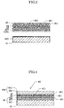
- FIG. 4 is a cross-sectional view illustrating an overview configuration of light-emitting element 4A according to Variation 1. Specifically, FIG. 4 corresponds to FIG. 2 . Note that, in the subsequent description, components that are essentially the same as light-emitting element 4 according to Embodiment share like reference numerals, and explanations thereof are omitted. The following only describes points different from Embodiment.
- Variation 1 describes light-emitting element 4A in which phosphor particles 451 are disposed on a side of phosphor layer 45a which is closer to substrate 41.
- phosphor layer 45a has a two-layer structure in which first layer 453 and second layer 454 are stacked.
- First layer 453 is formed from, for example, a light-transmissive plate material such as glass, and second layer 454 is formed from inorganic binder 455 containing many phosphor particles 451. Since second layer 454 is disposed on the side of phosphor layer 45a which is closer to substrate 41, and first layer 453 is disposed on the side of phosphor layer 45a which is away from substrate 41, phosphor particles 451 are disposed on the side of phosphor layer 45a which is closer to substrate 41.
- phosphor particles 451 are disposed closer to substrate 41 in phosphor layer 45a, the space between each of phosphor particles 451 and substrate 41 can be reduced. Therefore, heat can be efficiently transferred to a substrate 41 side of the light-emitting element.
- second layer 454 containing phosphor particles 451 can also be protected by first layer 453.
- phosphor layer 45a does not need to have the two-layer structure.
- phosphor particles may be collected toward one of the principal surfaces of the phosphor layer, and the principal surface may be disposed on the side of phosphor layer 45a which is closer to substrate 41.
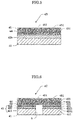
- FIG. 5 is a cross-sectional view illustrating an overview configuration of light-emitting element 4B according to Variation 2.
- FIG. 5 is a mere example and is not covered by the present invention. Specifically, FIG. 5 corresponds to FIG. 2 .
- joining part 42 includes first electrode layer 421, second electrode layer 422, and metal joining layer 423; as is the case in the present invention.
- Variation 2 describes light-emitting element 4B in which joining part 42b includes sintered silver nanoparticles
- Variation 2 is a mere example and is not part of the invention, defined by the appended claims.
- joining part 42b is interposed between adhesion layer 44 and substrate 41.
- joining part 42b is formed by sintering silver nanoparticles, joining with metal can be performed even without first electrode layer 421 and second electrode layer 422. Since reflectance of the silver nanoparticles is improved by being sintered, the silver nanoparticles can also serve as a reflecting layer. In other words, reflecting layer 43 in light-emitting element 4 according to Embodiment can be omitted, and thus manufacturing efficiency can be improved.
- FIG. 6 is a cross-sectional view illustrating an overview configuration of light-emitting element 4C according to Variation 3. Specifically, FIG. 6 corresponds to FIG. 2 .
- through hole 5 penetrates through substrate 41, joining part 42, reflecting layer 43, and adhesion layer 44 to extend continuously in a normal direction of primary surface 411 of substrate 41.
- Through hole 5 can serve as an optical path for excitation light (laser light) which enters from the substrate 41 side of the light-emitting element to excite phosphor particles 451 in phosphor layer 45. Accordingly, white light can be emitted to the travelling direction of excitation light.
- light source 2 and light guide member 3 can be disposed on the back side of substrate 41, the whole illumination device 1 can be made compact.
- through hole 5 may extend continuously in any direction as long as it is a direction that intersects with principal surface 411.
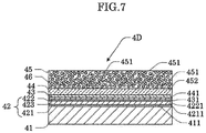
- FIG. 7 is a cross-sectional view illustrating an overview configuration of light-emitting element 4D according to Variation 4. Specifically, FIG. 7 corresponds to FIG. 2 .
- Light-emitting element 4D according to Variation 4 differs from light-emitting element 4 according to Embodiment in that light-emitting element 4D includes diffusion layer 46.
- light-emitting element 4D includes diffusion layer 46 which diffuses light and is interposed between phosphor layer 45 and adhesion layer 44.
- Diffusion layer 46 diffuses laser light which is excitation light, and fluorescence which is emitted by phosphor particles 451.
- Diffusion layer 46 is formed, for example, by dispersing diffusion particles such as silica-based particles or titanium-based particles in an inorganic sealing member such as glass. Since diffusion layer 46 is interposed between phosphor layer 45 and reflecting layer 43 as described above, the laser light and the fluorescence can be diffused by diffusion layer 46 and their light colors can be mixed. Therefore, uniform white light can be achieved.
- Variation 4 has described, as an example, the case where diffusion layer 46 is interposed between phosphor layer 45 and adhesion layer 44. However, it is sufficient that diffusion layer 46 is interposed between phosphor layer 45 and reflecting layer 43. In other words, diffusion layer 46 may be interposed between adhesion layer 44 and reflecting layer 43.
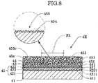
- FIG. 8 is a cross-sectional view illustrating an overview configuration of light-emitting element 4E according to Variation 5. Specifically, FIG. 8 corresponds to FIG. 2 .
- Light-emitting element 4E according to Variation 5 differs from light-emitting element 4 according to Embodiment in that the surface of phosphor layer 45e has uneven pattern 455. Specifically, as illustrated in FIG. 8 , uneven pattern 455 in which fine depressions and projections 454 are repeated is formed in region R1 on surface 453e of phosphor layer 45e which is a principal surface opposite to the principal surface of phosphor layer facing substrate 41. Region R1 is to be irradiated with laser light. Uneven pattern 455 is formed by the nanoimprint technique or blast processing, for example. The surface roughness of region R1 due to uneven pattern 455 may be a surface roughness having a wavelength greater than or equal to the wavelength of laser light. Accordingly, since laser light is diffused in region R1 on surface 453e of phosphor layer 45e, uniform white light can be achieved.
- uneven pattern 455 may be formed at least in region R1. In other words, uneven pattern 455 may be formed on the entire surface 453e of phosphor layer 45e.
- FIG. 9 is a cross-sectional view illustrating an overview configuration of light-emitting element 4F according to Variation 6. Specifically, FIG. 9 corresponds to FIG. 2 .
- Light-emitting element 4F according to Variation 6 differs from light-emitting element 4 according to Embodiment in that principal surface 452f of phosphor layer 45f has uneven pattern 459. Specifically, as illustrated in FIG. 9 , uneven pattern 459 in which minute depressions and projections 458 are repeated is formed in region R2 on principal surface 452f of phosphor layer 45f which faces substrate 41. Region R2 is to be irradiated with laser light. Uneven pattern 459 is formed by the nanoimprint technique or blast processing, for example. Surface roughness formed by uneven pattern 459 may be a surface roughness greater than or equal to the wavelength of laser light. Accordingly, since laser light is diffused in region R2 of principal surface 452f of phosphor layer 45f, uniform white light can be achieved.
- uneven pattern 459 may be formed in at least region R2. In other words, uneven pattern 459 may be formed on the entire principal surface 452f of phosphor layer 45f.
- Embodiment and Variations 1 to 6 have described as an example the case where light-emitting element 4 is applied to illumination device 1, light-emitting element 4 may also be used in other illumination systems. Examples of the other illumination systems include a projector, headlights mounted in vehicle, and so on. When light-emitting element 4 is applied to a projector, light-emitting element 4 is used as a phosphor wheel.
- a reflection inhibition layer such as an AR coat layer may be disposed on the surface of phosphor layer 45 which is opposite to principal surface 452 of phosphor layer 45, i.e., on the surface from which light is emitted. This improves the light extraction efficiency.
Landscapes
- Physics & Mathematics (AREA)
- Engineering & Computer Science (AREA)
- Optics & Photonics (AREA)
- General Engineering & Computer Science (AREA)
- General Physics & Mathematics (AREA)
- Spectroscopy & Molecular Physics (AREA)
- Microelectronics & Electronic Packaging (AREA)
- Chemical & Material Sciences (AREA)
- Dispersion Chemistry (AREA)
- Manufacturing & Machinery (AREA)
- Non-Portable Lighting Devices Or Systems Thereof (AREA)
- Led Device Packages (AREA)
Claims (8)
- Ein lichtemittierendes Element (4, 4A, 4B, 4C), das Folgendes umfasst:eine Phosphorschicht (45, 45a), die Phosphor mindestens eines Typs enthält;ein Substrat (41), das eine höhere Wärmeleitfähigkeit hat als die Phosphorschicht (45, 45a), wobei das Substrat (41) eine Hauptoberfläche (411) hat, über der die Phosphorschicht (45, 45a) angeordnet ist; undein Verbindungsteil (42, 42b), das zwischen der Phosphorschicht (45, 45a) und dem Substrat (41) angeordnet ist, um die Phosphorschicht (45, 45a) und das Substrat (41) zusammen mit Metall zu verbinden,wobei eine Haftschicht (44) und eine reflektierende Schicht (43) zwischen dem Verbindungsteil und der Phosphorschicht (45, 45a) angeordnet sind, wobei die Haftschicht (44) lichtdurchlässig ist und sich auf einer Hauptoberfläche (452, 452e) der Phosphorschicht (45, 45a) befindet, die dem Substrat (41) zugewandt ist, wobei sich die reflektierende Schicht (43) auf einer Hauptoberfläche (441) der Haftschicht (44) befindet, die dem Substrat (41) zugewandt ist, undwobei das Verbindungsteil (42, 42b) Folgendes enthält:eine erste Elektrodenschicht (421), die sich auf der Hauptoberfläche (411) des Substrats (41) befindet;eine zweite Elektrodenschicht (422), die sich auf einer Hauptoberfläche der reflektierenden Schicht (43) befindet, die dem Substrat (41) zugewandt ist; undeine metallische Verbindungsschicht (423), die zwischen der ersten Elektrodenschicht (421) und der zweiten Elektrodenschicht (422) angeordnet ist, um die erste Elektrodenschicht (421) und die zweite Elektrodenschicht (422) miteinander zu verbinden.
- Das lichtemittierende Element (4, 4A, 4B, 4C) nach Anspruch 1, wobei der Phosphor auf einer Seite der Phosphorschicht (45, 45a) angeordnet ist, die näher am Substrat (41) liegt.
- Das lichtemittierende Element (4, 4A, 4B, 4C) nach irgendeinem der Ansprüche von 1 bis 2,
wobei die Haftschicht (44) ein Metalloxid umfasst. - Das lichtemittierende Element (4, 4A, 4B, 4C) irgendeinem der Ansprüche von 1 bis 3,
wobei ein Durchgangsloch (5) das Substrat (41), das Verbindungsteil (42, 42b), die reflektierende Schicht (43) und die Haftschicht (44) durchdringt, um sich kontinuierlich in einer Richtung zu erstrecken, die die Hauptoberfläche (411) des Substrats (41) schneidet, und wobei
das Durchgangsloch (5) als optischer Pfad für Anregungslicht dient, das von einer Substratseite des lichtemittierenden Elements (4, 4A, 4B, 4C) eintritt, um den Phosphor anzuregen. - Das lichtemittierende Element (4, 4A, 4B, 4C) nach irgendeinem der Ansprüche von 1 bis 4,
wobei eine Diffusionsschicht (46), die Licht streut, zwischen der Phosphorschicht (45, 45a) und der reflektierenden Schicht (43) angeordnet ist. - Das lichtemittierende Element (4, 4A, 4B, 4C) nach irgendeinem der Ansprüche von 1 bis 5,
wobei eine Oberfläche der Phosphorschicht (45, 45a), die der Hauptoberfläche (452, 452e) der Phosphorschicht (45, 45a), die dem Substrat (41) zugewandt ist, gegenüberliegt, einen Bereich beinhaltet, der mit dem Anregungslicht zum Anregen des Phosphors zu bestrahlen ist, wobei der Bereich eine Oberflächenrauhigkeit mit einer Wellenlänge aufweist, die größer oder gleich einer Wellenlänge des Anregungslichts ist. - Das lichtemittierende Element (4, 4A, 4B, 4C) nach irgendeinem der Ansprüche von 1 bis 5,
wobei die Hauptoberfläche (452, 452e) der Phosphorschicht (45, 45a), die dem Substrat (41) zugewandt ist, einen Bereich beinhaltet, der mit dem Anregungslicht zum Anregen des Phosphors zu bestrahlen ist, wobei der Bereich eine Oberflächenrauhigkeit mit einer Wellenlänge aufweist, die größer oder gleich einer Wellenlänge des Anregungslichts ist. - Eine Beleuchtungsvorrichtung (1), die Folgendes umfasst:das lichtemittierende Element (4, 4A, 4B, 4C) nach irgendeinem der Ansprüche von 1 bis 7; undeine Lichtquelle (2), die Anregungslicht zur Anregung des Phosphors des lichtemittierenden Elements (4, 4A, 4B, 4C) aussendet.
Applications Claiming Priority (2)
| Application Number | Priority Date | Filing Date | Title |
|---|---|---|---|
| JP2015251803 | 2015-12-24 | ||
| PCT/JP2016/004853 WO2017110031A1 (ja) | 2015-12-24 | 2016-11-10 | 発光素子および照明装置 |
Publications (3)
| Publication Number | Publication Date |
|---|---|
| EP3396232A1 EP3396232A1 (de) | 2018-10-31 |
| EP3396232A4 EP3396232A4 (de) | 2018-12-26 |
| EP3396232B1 true EP3396232B1 (de) | 2020-06-17 |
Family
ID=59089928
Family Applications (1)
| Application Number | Title | Priority Date | Filing Date |
|---|---|---|---|
| EP16877936.1A Active EP3396232B1 (de) | 2015-12-24 | 2016-11-10 | Lichtemittierendes element und beleuchtungsvorrichtung |
Country Status (4)
| Country | Link |
|---|---|
| US (1) | US20200271282A1 (de) |
| EP (1) | EP3396232B1 (de) |
| JP (1) | JP6493713B2 (de) |
| WO (1) | WO2017110031A1 (de) |
Families Citing this family (10)
| Publication number | Priority date | Publication date | Assignee | Title |
|---|---|---|---|---|
| DE102017101729A1 (de) * | 2017-01-30 | 2018-08-02 | Osram Opto Semiconductors Gmbh | Strahlungsemittierende Vorrichtung |
| JP2019028096A (ja) * | 2017-07-25 | 2019-02-21 | 日本電気硝子株式会社 | 波長変換部材 |
| US11287107B2 (en) | 2018-02-14 | 2022-03-29 | Ngk Spark Plug Co., Ltd. | Optical wavelength conversion device |
| WO2020044426A1 (ja) * | 2018-08-28 | 2020-03-05 | 日本碍子株式会社 | 蛍光体素子および照明装置 |
| WO2020083717A1 (en) * | 2018-10-22 | 2020-04-30 | Lumileds Holding B.V. | A method of manufacturing a light converting device |
| CN115210888A (zh) * | 2020-03-18 | 2022-10-18 | 夏普株式会社 | 波长转换元件以及光学设备 |
| CN113970872A (zh) * | 2020-07-24 | 2022-01-25 | 中强光电股份有限公司 | 波长转换元件及投影机 |
| JP7535780B2 (ja) * | 2020-09-18 | 2024-08-19 | 株式会社オキサイド | 発光デバイスおよび光源デバイス |
| CN114967302A (zh) * | 2021-02-22 | 2022-08-30 | 中强光电股份有限公司 | 波长转换模块及投影机 |
| JPWO2025005047A1 (de) * | 2023-06-27 | 2025-01-02 |
Family Cites Families (8)
| Publication number | Priority date | Publication date | Assignee | Title |
|---|---|---|---|---|
| CN103080633A (zh) * | 2010-08-26 | 2013-05-01 | 日本电气硝子株式会社 | 波长变换元件、光源和液晶用背光单元 |
| JP2012243624A (ja) * | 2011-05-20 | 2012-12-10 | Stanley Electric Co Ltd | 光源装置および照明装置 |
| JP2012243701A (ja) * | 2011-05-24 | 2012-12-10 | Stanley Electric Co Ltd | 光源装置および照明装置 |
| JP6056117B2 (ja) * | 2012-12-06 | 2017-01-11 | スタンレー電気株式会社 | 発光装置及び車両用灯具 |
| WO2014123145A1 (ja) * | 2013-02-08 | 2014-08-14 | ウシオ電機株式会社 | 蛍光光源装置 |
| US20160102819A1 (en) * | 2013-04-24 | 2016-04-14 | Hitachi Maxell, Ltd. | Light source device and vehicle lamp |
| JP2015087423A (ja) * | 2013-10-28 | 2015-05-07 | セイコーエプソン株式会社 | 発光素子、照明装置およびプロジェクター |
| WO2018042826A1 (ja) * | 2016-08-30 | 2018-03-08 | パナソニックIpマネジメント株式会社 | 色変換素子及び照明装置 |
-
2016
- 2016-11-10 JP JP2017557682A patent/JP6493713B2/ja active Active
- 2016-11-10 WO PCT/JP2016/004853 patent/WO2017110031A1/ja not_active Ceased
- 2016-11-10 US US16/063,765 patent/US20200271282A1/en not_active Abandoned
- 2016-11-10 EP EP16877936.1A patent/EP3396232B1/de active Active
Non-Patent Citations (1)
| Title |
|---|
| None * |
Also Published As
| Publication number | Publication date |
|---|---|
| EP3396232A1 (de) | 2018-10-31 |
| US20200271282A1 (en) | 2020-08-27 |
| EP3396232A4 (de) | 2018-12-26 |
| JPWO2017110031A1 (ja) | 2018-06-21 |
| JP6493713B2 (ja) | 2019-04-03 |
| WO2017110031A1 (ja) | 2017-06-29 |
Similar Documents
| Publication | Publication Date | Title |
|---|---|---|
| EP3396232B1 (de) | Lichtemittierendes element und beleuchtungsvorrichtung | |
| US9785039B2 (en) | Wavelength conversion member, light emitting device, projector, and method of manufacturing wavelength conversion member | |
| TWI696685B (zh) | 光波長轉換裝置及光複合裝置 | |
| JP5530167B2 (ja) | 光源装置および照明装置 | |
| EP2933884B1 (de) | Lichtemittierende vorrichtung | |
| CN109328401B (zh) | 光转换封装 | |
| JP6371201B2 (ja) | 発光モジュール及びそれを用いた発光装置 | |
| CN105738994B (zh) | 波长转换装置及相关照明装置、荧光色轮和投影装置 | |
| JP2016058619A (ja) | 発光装置 | |
| CN110737085B (zh) | 波长转换装置 | |
| WO2015178223A1 (ja) | 波長変換部材及びそれを用いた発光装置 | |
| EP3189549B1 (de) | Lichtemittierende vorrichtung | |
| JP2016058624A (ja) | 発光装置 | |
| JP2012243701A (ja) | 光源装置および照明装置 | |
| JP2012104267A (ja) | 光源装置および照明装置 | |
| JP2014137973A (ja) | 光源装置 | |
| JP2018181711A (ja) | 蛍光体ホイール、及び、照明装置 | |
| JP5550368B2 (ja) | 光源装置および照明装置 | |
| CN107579144B (zh) | 烧结体和发光装置 | |
| WO2018042825A1 (ja) | 色変換素子 | |
| JP5021089B1 (ja) | 発光装置、照明装置、車両用前照灯、プロジェクタ、および、発光装置の製造方法 | |
| JP2013168602A (ja) | 光源装置および照明装置 | |
| JP6741982B2 (ja) | 発光素子および照明装置 | |
| JP2019003090A (ja) | 蛍光体素子の製造方法 | |
| CN113701125A (zh) | 透射式波长转换装置及其发光装置 |
Legal Events
| Date | Code | Title | Description |
|---|---|---|---|
| STAA | Information on the status of an ep patent application or granted ep patent |
Free format text: STATUS: THE INTERNATIONAL PUBLICATION HAS BEEN MADE |
|
| PUAI | Public reference made under article 153(3) epc to a published international application that has entered the european phase |
Free format text: ORIGINAL CODE: 0009012 |
|
| STAA | Information on the status of an ep patent application or granted ep patent |
Free format text: STATUS: REQUEST FOR EXAMINATION WAS MADE |
|
| 17P | Request for examination filed |
Effective date: 20180621 |
|
| AK | Designated contracting states |
Kind code of ref document: A1 Designated state(s): AL AT BE BG CH CY CZ DE DK EE ES FI FR GB GR HR HU IE IS IT LI LT LU LV MC MK MT NL NO PL PT RO RS SE SI SK SM TR |
|
| AX | Request for extension of the european patent |
Extension state: BA ME |
|
| A4 | Supplementary search report drawn up and despatched |
Effective date: 20181126 |
|
| RIC1 | Information provided on ipc code assigned before grant |
Ipc: H05B 33/14 20060101ALI20181120BHEP Ipc: H05B 33/24 20060101ALI20181120BHEP Ipc: H01L 51/56 20060101ALI20181120BHEP Ipc: G02B 5/02 20060101ALI20181120BHEP Ipc: F21Y 115/30 20160101ALI20181120BHEP Ipc: H05B 33/26 20060101ALI20181120BHEP Ipc: F21S 2/00 20160101ALI20181120BHEP Ipc: F21K 9/64 20160101AFI20181120BHEP Ipc: G02B 5/08 20060101ALI20181120BHEP Ipc: F21V 9/30 20180101ALI20181120BHEP |
|
| DAV | Request for validation of the european patent (deleted) | ||
| DAX | Request for extension of the european patent (deleted) | ||
| GRAP | Despatch of communication of intention to grant a patent |
Free format text: ORIGINAL CODE: EPIDOSNIGR1 |
|
| STAA | Information on the status of an ep patent application or granted ep patent |
Free format text: STATUS: GRANT OF PATENT IS INTENDED |
|
| INTG | Intention to grant announced |
Effective date: 20200129 |
|
| GRAS | Grant fee paid |
Free format text: ORIGINAL CODE: EPIDOSNIGR3 |
|
| GRAA | (expected) grant |
Free format text: ORIGINAL CODE: 0009210 |
|
| STAA | Information on the status of an ep patent application or granted ep patent |
Free format text: STATUS: THE PATENT HAS BEEN GRANTED |
|
| AK | Designated contracting states |
Kind code of ref document: B1 Designated state(s): AL AT BE BG CH CY CZ DE DK EE ES FI FR GB GR HR HU IE IS IT LI LT LU LV MC MK MT NL NO PL PT RO RS SE SI SK SM TR |
|
| REG | Reference to a national code |
Ref country code: GB Ref legal event code: FG4D |
|
| REG | Reference to a national code |
Ref country code: CH Ref legal event code: EP |
|
| REG | Reference to a national code |
Ref country code: DE Ref legal event code: R096 Ref document number: 602016038507 Country of ref document: DE |
|
| REG | Reference to a national code |
Ref country code: IE Ref legal event code: FG4D |
|
| REG | Reference to a national code |
Ref country code: AT Ref legal event code: REF Ref document number: 1281738 Country of ref document: AT Kind code of ref document: T Effective date: 20200715 |
|
| PG25 | Lapsed in a contracting state [announced via postgrant information from national office to epo] |
Ref country code: NO Free format text: LAPSE BECAUSE OF FAILURE TO SUBMIT A TRANSLATION OF THE DESCRIPTION OR TO PAY THE FEE WITHIN THE PRESCRIBED TIME-LIMIT Effective date: 20200917 Ref country code: LT Free format text: LAPSE BECAUSE OF FAILURE TO SUBMIT A TRANSLATION OF THE DESCRIPTION OR TO PAY THE FEE WITHIN THE PRESCRIBED TIME-LIMIT Effective date: 20200617 Ref country code: FI Free format text: LAPSE BECAUSE OF FAILURE TO SUBMIT A TRANSLATION OF THE DESCRIPTION OR TO PAY THE FEE WITHIN THE PRESCRIBED TIME-LIMIT Effective date: 20200617 Ref country code: SE Free format text: LAPSE BECAUSE OF FAILURE TO SUBMIT A TRANSLATION OF THE DESCRIPTION OR TO PAY THE FEE WITHIN THE PRESCRIBED TIME-LIMIT Effective date: 20200617 Ref country code: GR Free format text: LAPSE BECAUSE OF FAILURE TO SUBMIT A TRANSLATION OF THE DESCRIPTION OR TO PAY THE FEE WITHIN THE PRESCRIBED TIME-LIMIT Effective date: 20200918 |
|
| REG | Reference to a national code |
Ref country code: LT Ref legal event code: MG4D |
|
| REG | Reference to a national code |
Ref country code: NL Ref legal event code: MP Effective date: 20200617 |
|
| PG25 | Lapsed in a contracting state [announced via postgrant information from national office to epo] |
Ref country code: BG Free format text: LAPSE BECAUSE OF FAILURE TO SUBMIT A TRANSLATION OF THE DESCRIPTION OR TO PAY THE FEE WITHIN THE PRESCRIBED TIME-LIMIT Effective date: 20200917 Ref country code: RS Free format text: LAPSE BECAUSE OF FAILURE TO SUBMIT A TRANSLATION OF THE DESCRIPTION OR TO PAY THE FEE WITHIN THE PRESCRIBED TIME-LIMIT Effective date: 20200617 Ref country code: LV Free format text: LAPSE BECAUSE OF FAILURE TO SUBMIT A TRANSLATION OF THE DESCRIPTION OR TO PAY THE FEE WITHIN THE PRESCRIBED TIME-LIMIT Effective date: 20200617 Ref country code: HR Free format text: LAPSE BECAUSE OF FAILURE TO SUBMIT A TRANSLATION OF THE DESCRIPTION OR TO PAY THE FEE WITHIN THE PRESCRIBED TIME-LIMIT Effective date: 20200617 |
|
| REG | Reference to a national code |
Ref country code: AT Ref legal event code: MK05 Ref document number: 1281738 Country of ref document: AT Kind code of ref document: T Effective date: 20200617 |
|
| PG25 | Lapsed in a contracting state [announced via postgrant information from national office to epo] |
Ref country code: NL Free format text: LAPSE BECAUSE OF FAILURE TO SUBMIT A TRANSLATION OF THE DESCRIPTION OR TO PAY THE FEE WITHIN THE PRESCRIBED TIME-LIMIT Effective date: 20200617 Ref country code: AL Free format text: LAPSE BECAUSE OF FAILURE TO SUBMIT A TRANSLATION OF THE DESCRIPTION OR TO PAY THE FEE WITHIN THE PRESCRIBED TIME-LIMIT Effective date: 20200617 |
|
| PG25 | Lapsed in a contracting state [announced via postgrant information from national office to epo] |
Ref country code: SM Free format text: LAPSE BECAUSE OF FAILURE TO SUBMIT A TRANSLATION OF THE DESCRIPTION OR TO PAY THE FEE WITHIN THE PRESCRIBED TIME-LIMIT Effective date: 20200617 Ref country code: AT Free format text: LAPSE BECAUSE OF FAILURE TO SUBMIT A TRANSLATION OF THE DESCRIPTION OR TO PAY THE FEE WITHIN THE PRESCRIBED TIME-LIMIT Effective date: 20200617 Ref country code: CZ Free format text: LAPSE BECAUSE OF FAILURE TO SUBMIT A TRANSLATION OF THE DESCRIPTION OR TO PAY THE FEE WITHIN THE PRESCRIBED TIME-LIMIT Effective date: 20200617 Ref country code: IT Free format text: LAPSE BECAUSE OF FAILURE TO SUBMIT A TRANSLATION OF THE DESCRIPTION OR TO PAY THE FEE WITHIN THE PRESCRIBED TIME-LIMIT Effective date: 20200617 Ref country code: RO Free format text: LAPSE BECAUSE OF FAILURE TO SUBMIT A TRANSLATION OF THE DESCRIPTION OR TO PAY THE FEE WITHIN THE PRESCRIBED TIME-LIMIT Effective date: 20200617 Ref country code: EE Free format text: LAPSE BECAUSE OF FAILURE TO SUBMIT A TRANSLATION OF THE DESCRIPTION OR TO PAY THE FEE WITHIN THE PRESCRIBED TIME-LIMIT Effective date: 20200617 Ref country code: PT Free format text: LAPSE BECAUSE OF FAILURE TO SUBMIT A TRANSLATION OF THE DESCRIPTION OR TO PAY THE FEE WITHIN THE PRESCRIBED TIME-LIMIT Effective date: 20201019 Ref country code: ES Free format text: LAPSE BECAUSE OF FAILURE TO SUBMIT A TRANSLATION OF THE DESCRIPTION OR TO PAY THE FEE WITHIN THE PRESCRIBED TIME-LIMIT Effective date: 20200617 |
|
| PG25 | Lapsed in a contracting state [announced via postgrant information from national office to epo] |
Ref country code: PL Free format text: LAPSE BECAUSE OF FAILURE TO SUBMIT A TRANSLATION OF THE DESCRIPTION OR TO PAY THE FEE WITHIN THE PRESCRIBED TIME-LIMIT Effective date: 20200617 Ref country code: SK Free format text: LAPSE BECAUSE OF FAILURE TO SUBMIT A TRANSLATION OF THE DESCRIPTION OR TO PAY THE FEE WITHIN THE PRESCRIBED TIME-LIMIT Effective date: 20200617 Ref country code: IS Free format text: LAPSE BECAUSE OF FAILURE TO SUBMIT A TRANSLATION OF THE DESCRIPTION OR TO PAY THE FEE WITHIN THE PRESCRIBED TIME-LIMIT Effective date: 20201017 |
|
| REG | Reference to a national code |
Ref country code: DE Ref legal event code: R097 Ref document number: 602016038507 Country of ref document: DE |
|
| PLBE | No opposition filed within time limit |
Free format text: ORIGINAL CODE: 0009261 |
|
| STAA | Information on the status of an ep patent application or granted ep patent |
Free format text: STATUS: NO OPPOSITION FILED WITHIN TIME LIMIT |
|
| PG25 | Lapsed in a contracting state [announced via postgrant information from national office to epo] |
Ref country code: DK Free format text: LAPSE BECAUSE OF FAILURE TO SUBMIT A TRANSLATION OF THE DESCRIPTION OR TO PAY THE FEE WITHIN THE PRESCRIBED TIME-LIMIT Effective date: 20200617 |
|
| 26N | No opposition filed |
Effective date: 20210318 |
|
| PG25 | Lapsed in a contracting state [announced via postgrant information from national office to epo] |
Ref country code: SI Free format text: LAPSE BECAUSE OF FAILURE TO SUBMIT A TRANSLATION OF THE DESCRIPTION OR TO PAY THE FEE WITHIN THE PRESCRIBED TIME-LIMIT Effective date: 20200617 |
|
| PG25 | Lapsed in a contracting state [announced via postgrant information from national office to epo] |
Ref country code: MC Free format text: LAPSE BECAUSE OF FAILURE TO SUBMIT A TRANSLATION OF THE DESCRIPTION OR TO PAY THE FEE WITHIN THE PRESCRIBED TIME-LIMIT Effective date: 20200617 |
|
| REG | Reference to a national code |
Ref country code: CH Ref legal event code: PL |
|
| GBPC | Gb: european patent ceased through non-payment of renewal fee |
Effective date: 20201110 |
|
| PG25 | Lapsed in a contracting state [announced via postgrant information from national office to epo] |
Ref country code: LU Free format text: LAPSE BECAUSE OF NON-PAYMENT OF DUE FEES Effective date: 20201110 |
|
| PG25 | Lapsed in a contracting state [announced via postgrant information from national office to epo] |
Ref country code: LI Free format text: LAPSE BECAUSE OF NON-PAYMENT OF DUE FEES Effective date: 20201130 Ref country code: CH Free format text: LAPSE BECAUSE OF NON-PAYMENT OF DUE FEES Effective date: 20201130 |
|
| PG25 | Lapsed in a contracting state [announced via postgrant information from national office to epo] |
Ref country code: IE Free format text: LAPSE BECAUSE OF NON-PAYMENT OF DUE FEES Effective date: 20201110 Ref country code: FR Free format text: LAPSE BECAUSE OF NON-PAYMENT OF DUE FEES Effective date: 20201130 |
|
| PG25 | Lapsed in a contracting state [announced via postgrant information from national office to epo] |
Ref country code: GB Free format text: LAPSE BECAUSE OF NON-PAYMENT OF DUE FEES Effective date: 20201110 |
|
| PG25 | Lapsed in a contracting state [announced via postgrant information from national office to epo] |
Ref country code: IS Free format text: LAPSE BECAUSE OF FAILURE TO SUBMIT A TRANSLATION OF THE DESCRIPTION OR TO PAY THE FEE WITHIN THE PRESCRIBED TIME-LIMIT Effective date: 20201017 Ref country code: TR Free format text: LAPSE BECAUSE OF FAILURE TO SUBMIT A TRANSLATION OF THE DESCRIPTION OR TO PAY THE FEE WITHIN THE PRESCRIBED TIME-LIMIT Effective date: 20200617 Ref country code: MT Free format text: LAPSE BECAUSE OF FAILURE TO SUBMIT A TRANSLATION OF THE DESCRIPTION OR TO PAY THE FEE WITHIN THE PRESCRIBED TIME-LIMIT Effective date: 20200617 Ref country code: CY Free format text: LAPSE BECAUSE OF FAILURE TO SUBMIT A TRANSLATION OF THE DESCRIPTION OR TO PAY THE FEE WITHIN THE PRESCRIBED TIME-LIMIT Effective date: 20200617 |
|
| PG25 | Lapsed in a contracting state [announced via postgrant information from national office to epo] |
Ref country code: MK Free format text: LAPSE BECAUSE OF FAILURE TO SUBMIT A TRANSLATION OF THE DESCRIPTION OR TO PAY THE FEE WITHIN THE PRESCRIBED TIME-LIMIT Effective date: 20200617 |
|
| PGFP | Annual fee paid to national office [announced via postgrant information from national office to epo] |
Ref country code: DE Payment date: 20251119 Year of fee payment: 10 |
|
| PGFP | Annual fee paid to national office [announced via postgrant information from national office to epo] |
Ref country code: BE Payment date: 20251119 Year of fee payment: 10 |