EP3373357A1 - Hocheffizienter gelblichtemitter für oled-vorrichtungen - Google Patents
Hocheffizienter gelblichtemitter für oled-vorrichtungen Download PDFInfo
- Publication number
- EP3373357A1 EP3373357A1 EP18164372.7A EP18164372A EP3373357A1 EP 3373357 A1 EP3373357 A1 EP 3373357A1 EP 18164372 A EP18164372 A EP 18164372A EP 3373357 A1 EP3373357 A1 EP 3373357A1
- Authority
- EP
- European Patent Office
- Prior art keywords
- compound
- consumer product
- alkyl
- organic
- cycloalkyl
- Prior art date
- Legal status (The legal status is an assumption and is not a legal conclusion. Google has not performed a legal analysis and makes no representation as to the accuracy of the status listed.)
- Granted
Links
- 0 CCC(CC)(C1c2ccccc2-c2*(C)ccc(-c3cc(*)c(C)c(*)c3)c2)*(cc(*)c(*)c2*)c2-c2c1cccc2 Chemical compound CCC(CC)(C1c2ccccc2-c2*(C)ccc(-c3cc(*)c(C)c(*)c3)c2)*(cc(*)c(*)c2*)c2-c2c1cccc2 0.000 description 15
- NSXJEEMTGWMJPY-UHFFFAOYSA-N c(cc1)cc(c2c3cccc2)c1[n]3-c1cccc(-c2cccc(-[n]3c(cccc4)c4c4c3cccc4)c2)c1 Chemical compound c(cc1)cc(c2c3cccc2)c1[n]3-c1cccc(-c2cccc(-[n]3c(cccc4)c4c4c3cccc4)c2)c1 NSXJEEMTGWMJPY-UHFFFAOYSA-N 0.000 description 2
- JBIGWFLWHIBPRJ-UHFFFAOYSA-N CN[O]([I]=C)[IH]([O](N)[I]=C)=C Chemical compound CN[O]([I]=C)[IH]([O](N)[I]=C)=C JBIGWFLWHIBPRJ-UHFFFAOYSA-N 0.000 description 1
- QKVWPNRUXZYLQV-UHFFFAOYSA-N c(cc1)cc(c2ccc3)c1[s]c2c3-c1cccc(-c2ccc(c3ccccc3c3c4cccc3)c4c2)c1 Chemical compound c(cc1)cc(c2ccc3)c1[s]c2c3-c1cccc(-c2ccc(c3ccccc3c3c4cccc3)c4c2)c1 QKVWPNRUXZYLQV-UHFFFAOYSA-N 0.000 description 1
- RNJALDUDQIQBDE-UHFFFAOYSA-N c(cc1)ccc1[Si](c1ccccc1)(c1cc(-c2cccc3c2[s]c2ccccc32)ccc1)c1cc(-c2cccc3c2[s]c2c3cccc2)ccc1 Chemical compound c(cc1)ccc1[Si](c1ccccc1)(c1cc(-c2cccc3c2[s]c2ccccc32)ccc1)c1cc(-c2cccc3c2[s]c2c3cccc2)ccc1 RNJALDUDQIQBDE-UHFFFAOYSA-N 0.000 description 1
Images


Classifications
-
- C—CHEMISTRY; METALLURGY
- C07—ORGANIC CHEMISTRY
- C07F—ACYCLIC, CARBOCYCLIC OR HETEROCYCLIC COMPOUNDS CONTAINING ELEMENTS OTHER THAN CARBON, HYDROGEN, HALOGEN, OXYGEN, NITROGEN, SULFUR, SELENIUM OR TELLURIUM
- C07F15/00—Compounds containing elements of Groups 8, 9, 10 or 18 of the Periodic System
- C07F15/0006—Compounds containing elements of Groups 8, 9, 10 or 18 of the Periodic System compounds of the platinum group
- C07F15/0033—Iridium compounds
-
- C—CHEMISTRY; METALLURGY
- C09—DYES; PAINTS; POLISHES; NATURAL RESINS; ADHESIVES; COMPOSITIONS NOT OTHERWISE PROVIDED FOR; APPLICATIONS OF MATERIALS NOT OTHERWISE PROVIDED FOR
- C09K—MATERIALS FOR MISCELLANEOUS APPLICATIONS, NOT PROVIDED FOR ELSEWHERE
- C09K11/00—Luminescent, e.g. electroluminescent, chemiluminescent materials
- C09K11/06—Luminescent, e.g. electroluminescent, chemiluminescent materials containing organic luminescent materials
-
- H—ELECTRICITY
- H05—ELECTRIC TECHNIQUES NOT OTHERWISE PROVIDED FOR
- H05B—ELECTRIC HEATING; ELECTRIC LIGHT SOURCES NOT OTHERWISE PROVIDED FOR; CIRCUIT ARRANGEMENTS FOR ELECTRIC LIGHT SOURCES, IN GENERAL
- H05B33/00—Electroluminescent light sources
- H05B33/12—Light sources with substantially two-dimensional radiating surfaces
- H05B33/14—Light sources with substantially two-dimensional radiating surfaces characterised by the chemical or physical composition or the arrangement of the electroluminescent material, or by the simultaneous addition of the electroluminescent material in or onto the light source
-
- H—ELECTRICITY
- H10—SEMICONDUCTOR DEVICES; ELECTRIC SOLID-STATE DEVICES NOT OTHERWISE PROVIDED FOR
- H10K—ORGANIC ELECTRIC SOLID-STATE DEVICES
- H10K50/00—Organic light-emitting devices
- H10K50/10—OLEDs or polymer light-emitting diodes [PLED]
- H10K50/11—OLEDs or polymer light-emitting diodes [PLED] characterised by the electroluminescent [EL] layers
-
- H—ELECTRICITY
- H10—SEMICONDUCTOR DEVICES; ELECTRIC SOLID-STATE DEVICES NOT OTHERWISE PROVIDED FOR
- H10K—ORGANIC ELECTRIC SOLID-STATE DEVICES
- H10K85/00—Organic materials used in the body or electrodes of devices covered by this subclass
- H10K85/30—Coordination compounds
- H10K85/341—Transition metal complexes, e.g. Ru(II)polypyridine complexes
- H10K85/342—Transition metal complexes, e.g. Ru(II)polypyridine complexes comprising iridium
-
- C—CHEMISTRY; METALLURGY
- C09—DYES; PAINTS; POLISHES; NATURAL RESINS; ADHESIVES; COMPOSITIONS NOT OTHERWISE PROVIDED FOR; APPLICATIONS OF MATERIALS NOT OTHERWISE PROVIDED FOR
- C09K—MATERIALS FOR MISCELLANEOUS APPLICATIONS, NOT PROVIDED FOR ELSEWHERE
- C09K2211/00—Chemical nature of organic luminescent or tenebrescent compounds
- C09K2211/10—Non-macromolecular compounds
- C09K2211/1003—Carbocyclic compounds
- C09K2211/1007—Non-condensed systems
-
- C—CHEMISTRY; METALLURGY
- C09—DYES; PAINTS; POLISHES; NATURAL RESINS; ADHESIVES; COMPOSITIONS NOT OTHERWISE PROVIDED FOR; APPLICATIONS OF MATERIALS NOT OTHERWISE PROVIDED FOR
- C09K—MATERIALS FOR MISCELLANEOUS APPLICATIONS, NOT PROVIDED FOR ELSEWHERE
- C09K2211/00—Chemical nature of organic luminescent or tenebrescent compounds
- C09K2211/10—Non-macromolecular compounds
- C09K2211/1003—Carbocyclic compounds
- C09K2211/1011—Condensed systems
-
- C—CHEMISTRY; METALLURGY
- C09—DYES; PAINTS; POLISHES; NATURAL RESINS; ADHESIVES; COMPOSITIONS NOT OTHERWISE PROVIDED FOR; APPLICATIONS OF MATERIALS NOT OTHERWISE PROVIDED FOR
- C09K—MATERIALS FOR MISCELLANEOUS APPLICATIONS, NOT PROVIDED FOR ELSEWHERE
- C09K2211/00—Chemical nature of organic luminescent or tenebrescent compounds
- C09K2211/10—Non-macromolecular compounds
- C09K2211/1018—Heterocyclic compounds
- C09K2211/1025—Heterocyclic compounds characterised by ligands
- C09K2211/1029—Heterocyclic compounds characterised by ligands containing one nitrogen atom as the heteroatom
-
- C—CHEMISTRY; METALLURGY
- C09—DYES; PAINTS; POLISHES; NATURAL RESINS; ADHESIVES; COMPOSITIONS NOT OTHERWISE PROVIDED FOR; APPLICATIONS OF MATERIALS NOT OTHERWISE PROVIDED FOR
- C09K—MATERIALS FOR MISCELLANEOUS APPLICATIONS, NOT PROVIDED FOR ELSEWHERE
- C09K2211/00—Chemical nature of organic luminescent or tenebrescent compounds
- C09K2211/18—Metal complexes
- C09K2211/185—Metal complexes of the platinum group, i.e. Os, Ir, Pt, Ru, Rh or Pd
-
- H—ELECTRICITY
- H10—SEMICONDUCTOR DEVICES; ELECTRIC SOLID-STATE DEVICES NOT OTHERWISE PROVIDED FOR
- H10K—ORGANIC ELECTRIC SOLID-STATE DEVICES
- H10K2101/00—Properties of the organic materials covered by group H10K85/00
- H10K2101/10—Triplet emission
-
- H—ELECTRICITY
- H10—SEMICONDUCTOR DEVICES; ELECTRIC SOLID-STATE DEVICES NOT OTHERWISE PROVIDED FOR
- H10K—ORGANIC ELECTRIC SOLID-STATE DEVICES
- H10K85/00—Organic materials used in the body or electrodes of devices covered by this subclass
- H10K85/60—Organic compounds having low molecular weight
- H10K85/615—Polycyclic condensed aromatic hydrocarbons, e.g. anthracene
- H10K85/622—Polycyclic condensed aromatic hydrocarbons, e.g. anthracene containing four rings, e.g. pyrene
-
- H—ELECTRICITY
- H10—SEMICONDUCTOR DEVICES; ELECTRIC SOLID-STATE DEVICES NOT OTHERWISE PROVIDED FOR
- H10K—ORGANIC ELECTRIC SOLID-STATE DEVICES
- H10K85/00—Organic materials used in the body or electrodes of devices covered by this subclass
- H10K85/60—Organic compounds having low molecular weight
- H10K85/649—Aromatic compounds comprising a hetero atom
- H10K85/657—Polycyclic condensed heteroaromatic hydrocarbons
- H10K85/6576—Polycyclic condensed heteroaromatic hydrocarbons comprising only sulfur in the heteroaromatic polycondensed ring system, e.g. benzothiophene
-
- Y—GENERAL TAGGING OF NEW TECHNOLOGICAL DEVELOPMENTS; GENERAL TAGGING OF CROSS-SECTIONAL TECHNOLOGIES SPANNING OVER SEVERAL SECTIONS OF THE IPC; TECHNICAL SUBJECTS COVERED BY FORMER USPC CROSS-REFERENCE ART COLLECTIONS [XRACs] AND DIGESTS
- Y02—TECHNOLOGIES OR APPLICATIONS FOR MITIGATION OR ADAPTATION AGAINST CLIMATE CHANGE
- Y02E—REDUCTION OF GREENHOUSE GAS [GHG] EMISSIONS, RELATED TO ENERGY GENERATION, TRANSMISSION OR DISTRIBUTION
- Y02E10/00—Energy generation through renewable energy sources
- Y02E10/50—Photovoltaic [PV] energy
- Y02E10/549—Organic PV cells
Definitions
- the claimed invention was made by, on behalf of, and/or in connection with one or more of the following parties to a joint university corporation research agreement: Regents of the University of Michigan, Princeton University, The University of Southern California, and the Universal Display Corporation. The agreement was in effect on and before the date the claimed invention was made, and the claimed invention was made as a result of activities undertaken within the scope of the agreement.
- the present invention relates to heteroleptic iridium complexes containing phenylpyridine ligands. These heteroleptic iridium complexes are useful as dopants in OLED devices.
- Opto-electronic devices that make use of organic materials are becoming increasingly desirable for a number of reasons. Many of the materials used to make such devices are relatively inexpensive, so organic opto-electronic devices have the potential for cost advantages over inorganic devices. In addition, the inherent properties of organic materials, such as their flexibility, may make them well suited for particular applications such as fabrication on a flexible substrate. Examples of organic opto-electronic devices include organic light emitting devices (OLEDs), organic phototransistors, organic photovoltaic cells, and organic photodetectors. For OLEDs, the organic materials may have performance advantages over conventional materials. For example, the wavelength at which an organic emissive layer emits light may generally be readily tuned with appropriate dopants.
- OLEDs organic light emitting devices
- the wavelength at which an organic emissive layer emits light may generally be readily tuned with appropriate dopants.
- OLEDs make use of thin organic films that emit light when voltage is applied across the device. OLEDs are becoming an increasingly interesting technology for use in applications such as flat panel displays, illumination, and backlighting. Several OLED materials and configurations are described in U.S. Pat. Nos. 5,844,363 , 6,303,238 , and 5,707,745 , which are incorporated herein by reference in their entirety.
- phosphorescent emissive molecules is a full color display.
- Industry standards for such a display call for pixels adapted to emit particular colors, referred to as "saturated" colors.
- these standards call for saturated red, green, and blue pixels. Color may be measured using CIE coordinates, which are well known to the art.
- a green emissive molecule is tris(2-phenylpyridine) iridium, denoted Ir(ppy) 3 , which has the following structure:
- organic includes polymeric materials as well as small molecule organic materials that may be used to fabricate organic opto-electronic devices.
- Small molecule refers to any organic material that is not a polymer, and "small molecules” may actually be quite large. Small molecules may include repeat units in some circumstances. For example, using a long chain alkyl group as a substituent does not remove a molecule from the "small molecule” class. Small molecules may also be incorporated into polymers, for example as a pendent group on a polymer backbone or as a part of the backbone. Small molecules may also serve as the core moiety of a dendrimer, which consists of a series of chemical shells built on the core moiety.
- the core moiety of a dendrimer may be a fluorescent or phosphorescent small molecule emitter.
- a dendrimer may be a "small molecule,” and it is believed that all dendrimers currently used in the field of OLEDs are small molecules.
- top means furthest away from the substrate, while “bottom” means closest to the substrate.
- first layer is described as “disposed over” a second layer, the first layer is disposed further away from substrate. There may be other layers between the first and second layer, unless it is specified that the first layer is "in contact with” the second layer.
- a cathode may be described as “disposed over” an anode, even though there are various organic layers in between.
- solution processible means capable of being dissolved, dispersed, or transported in and/or deposited from a liquid medium, either in solution or suspension form.
- a ligand may be referred to as "photoactive” when it is believed that the ligand directly contributes to the photoactive properties of an emissive material.
- a ligand may be referred to as "ancillary” when it is believed that the ligand does not contribute to the photoactive properties of an emissive material, although an ancillary ligand may alter the properties of a photoactive ligand.
- a first "Highest Occupied Molecular Orbital” (HOMO) or “Lowest Unoccupied Molecular Orbital” (LUMO) energy level is “greater than” or "higher than” a second HOMO or LUMO energy level if the first energy level is closer to the vacuum energy level.
- IP ionization potentials
- a higher HOMO energy level corresponds to an IP having a smaller absolute value (an IP that is less negative).
- a higher LUMO energy level corresponds to an electron affinity (EA) having a smaller absolute value (an EA that is less negative).
- the LUMO energy level of a material is higher than the HOMO energy level of the same material.
- a "higher” HOMO or LUMO energy level appears closer to the top of such a diagram than a "lower” HOMO or LUMO energy level.
- a first work function is "greater than” or “higher than” a second work function if the first work function has a higher absolute value. Because work functions are generally measured as negative numbers relative to vacuum level, this means that a "higher” work function is more negative. On a conventional energy level diagram, with the vacuum level at the top, a “higher” work function is illustrated as further away from the vacuum level in the downward direction. Thus, the definitions of HOMO and LUMO energy levels follow a different convention than work functions.
- a compound comprising a heteroleptic iridium complex is provided.
- the compound is a compound of Formula I.
- R 1 , R 2 , R 3 , R 4 , R 5 , and R 6 are independently selected from the group consisting of hydrogen, deuterium, cycloalkyl, deuterated cycloalkyl, alkyl, and deuterated alkyl.
- At least one of R 1 , R 2 , R 3 , R 4 , R 5 , and R 6 is cycloalkyl, deuterated cycloalkyl, alkyl or deuterated alkyl, and any two adjacent R 1 , R 2 , R 3 , R 4 , R 5 , and R 6 are optionally linked together to form a ring.
- Ring A is attached to the 4- or 5-position of ring B.
- R and R' represent mono-, di-, tri- or tetra-substitution and are independently selected from the group consisting of: hydrogen, deuterium, halide, alkyl, cycloalkyl, heteroalkyl, arylalkyl, alkoxy, aryloxy, amino, silyl, alkenyl, cycloalkenyl, heteroalkenyl, alkynyl, aryl, heteroaryl, acyl, carbonyl, carboxylic acids, ester, nitrile, isonitrile, sulfanyl, sulfinyl, sulfonyl, phosphino, and combinations thereof.
- the compound is a compound of Formula II.
- the compound is a compound of Formula III.
- R 1 is alkyl.
- R 2 is alkyl.
- R 3 is alkyl.
- R 4 is alkyl.
- R 5 is alkyl.
- R 6 is alkyl.
- at least one of R 1 , R 2 , and R 3 is alkyl.
- at least one of R 4 , R 5 , and R 6 is alkyl.
- at least one of R 1 , R 2 , and R 3 is alkyl and at least one of R 4 , R 5 , and R 6 is alkyl.
- the alkyl contains at least 2 carbons, at least 3 carbons, or at most 6 carbons. In another aspect, the alkyl contains greater than 10 carbons.
- the compound emits yellow light with a full width at half maximum between about 70 nm to about 110 nm when the light has a peak wavelength between about 530 nm to about 580 nm.
- the compound is selected from Compound 1 - Compound 89.
- a first device comprises a first organic light emitting device, and contains an anode, a cathode, and an organic layer, disposed between the anode and the cathode, comprising a compound having a formula of Formula I:
- R 1 , R 2 , R 3 , R 4 , R 5 , and R 6 are independently selected from the group consisting of hydrogen, deuterium, cycloalkyl, deuterated cycloalkyl, alkyl, and deuterated alkyl.
- At least one of R 1 , R 2 , R 3 , R 4 , R 5 , and R 6 is cycloalkyl, deuterated cycloalkyl, alkyl or deuterated alkyl, and any two adjacent R 1 , R 2 , R 3 , R 4 , R 5 , and R 6 are optionally linked together to form a ring.
- Ring A is attached to the 4- or 5-position of ring B.
- R and R' represent mono-, di-, tri- or tetra-substitution and are independently selected from the group consisting of: hydrogen, deuterium, halide, alkyl, cycloalkyl, heteroalkyl, arylalkyl, alkoxy, aryloxy, amino, silyl, alkenyl, cycloalkenyl, heteroalkenyl, alkynyl, aryl, heteroaryl, acyl, carbonyl, carboxylic acids, ester, nitrile, isonitrile, sulfanyl, sulfinyl, sulfonyl, phosphino, and combinations thereof.
- the organic layer is an emissive layer and the compound is an emissive dopant. In another aspect, the organic layer is an emissive layer and the compound is an non-emissive dopant.
- the organic layer further comprises a host.
- Ar 1 and Ar 2 are independently selected from the group consisting of benzene, biphenyl, naphthalene, triphenylene, carbazole, and heteroaromatic analogs thereof, and n is from 1 to 10.
- the host has the formula:
- the host is a metal complex.
- the first device is a consumer product. In another aspect, the first device is an organic light-emitting device. In another aspect, the first device comprises a lighting panel.
- the first device further comprises a second emissive dopant having a peak wavelength of between 400 to 500 nanometers.
- the second emissive dopant is a fluorescent emitter.
- the second emissive dopant is a phosphorescent emitter.
- the first device further comprises a first organic light-emitting device comprising a compound of Formula I and a second light emitting device separate from the first organic light-emitting device comprising an emissive dopant having a peak wavelength of between 400 to 500 nanometers.
- the first device comprises an organic-light emitting device having a first emissive layer compring a compound of Formula I and a second emissive layer comprising an emissive dopant having a peak wavelength of between 400 to 500 nanometers.
- an OLED comprises at least one organic layer disposed between and electrically connected to an anode and a cathode.
- the anode injects holes and the cathode injects electrons into the organic layer(s).
- the injected holes and electrons each migrate toward the oppositely charged electrode.
- an "exciton” which is a localized electron-hole pair having an excited energy state, is formed.
- Light is emitted when the exciton relaxes via a photoemissive mechanism.
- the exciton may be localized on an excimer or an exciplex. Non-radiative mechanisms, such as thermal relaxation, may also occur, but are generally considered undesirable.
- the initial OLEDs used emissive molecules that emitted light from their singlet states ("fluorescence") as disclosed, for example, in U.S. Pat. No. 4,769,292 , which is incorporated by reference in its entirety. Fluorescent emission generally occurs in a time frame of less than 10 nanoseconds.
- FIG. 1 shows an organic light emitting device 100.
- Device 100 may include a substrate 110, an anode 115, a hole injection layer 120, a hole transport layer 125, an electron blocking layer 130, an emissive layer 135, a hole blocking layer 140, an electron transport layer 145, an electron injection layer 150, a protective layer 155, and a cathode 160.
- Cathode 160 is a compound cathode having a first conductive layer 162 and a second conductive layer 164.
- Device 100 may be fabricated by depositing the layers described, in order. The properties and functions of these various layers, as well as example materials, are described in more detail in US 7,279,704 at cols. 6-10, which are incorporated by reference.
- each of these layers are available.
- a flexible and transparent substrate-anode combination is disclosed in U.S. Pat. No. 5,844,363 , which is incorporated by reference in its entirety.
- An example of a p-doped hole transport layer is m-MTDATA doped with F.sub.4-TCNQ at a molar ratio of 50:1, as disclosed in U.S. Patent Application Publication No. 2003/0230980 , which is incorporated by reference in its entirety.
- Examples of emissive and host materials are disclosed in U.S. Pat. No. 6,303,238 to Thompson et al. , which is incorporated by reference in its entirety.
- An example of an n-doped electron transport layer is BPhen doped with Li at a molar ratio of 1:1, as disclosed in U.S. Patent Application Publication No. 2003/0230980 , which is incorporated by reference in its entirety.
- U.S. Pat. Nos. 5,703,436 and 5,707,745 which are incorporated by reference in their entireties, disclose examples of cathodes including compound cathodes having a thin layer of metal such as Mg:Ag with an overlying transparent, electrically-conductive, sputter-deposited ITO layer.
- the theory and use of blocking layers is described in more detail in U.S. Pat. No. 6,097,147 and U.S. Patent Application Publication No.
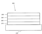
- FIG. 2 shows an inverted OLED 200.
- the device includes a substrate 210, a cathode 215, an emissive layer 220, a hole transport layer 225, and an anode 230.
- Device 200 may be fabricated by depositing the layers described, in order. Because the most common OLED configuration has a cathode disposed over the anode, and device 200 has cathode 215 disposed under anode 230, device 200 may be referred to as an "inverted" OLED. Materials similar to those described with respect to device 100 may be used in the corresponding layers of device 200.
- FIG. 2 provides one example of how some layers may be omitted from the structure of device 100.
- FIGS. 1 and 2 The simple layered structure illustrated in FIGS. 1 and 2 is provided by way of non-limiting example, and it is understood that embodiments of the invention may be used in connection with a wide variety of other structures.
- the specific materials and structures described are exemplary in nature, and other materials and structures may be used.
- Functional OLEDs may be achieved by combining the various layers described in different ways, or layers may be omitted entirely, based on design, performance, and cost factors. Other layers not specifically described may also be included. Materials other than those specifically described may be used. Although many of the examples provided herein describe various layers as comprising a single material, it is understood that combinations of materials, such as a mixture of host and dopant, or more generally a mixture, may be used. Also, the layers may have various sublayers.
- hole transport layer 225 transports holes and injects holes into emissive layer 220, and may be described as a hole transport layer or a hole injection layer.
- an OLED may be described as having an "organic layer" disposed between a cathode and an anode. This organic layer may comprise a single layer, or may further comprise multiple layers of different organic materials as described, for example, with respect to FIGS. 1 and 2 .
- OLEDs comprised of polymeric materials (PLEDs) such as disclosed in U.S. Pat. No. 5,247,190 to Friend et al. , which is incorporated by reference in its entirety.
- PLEDs polymeric materials
- OLEDs having a single organic layer may be used.
- OLEDs may be stacked, for example as described in U.S. Pat. No. 5,707,745 to Forrest et al , which is incorporated by reference in its entirety.
- the OLED structure may deviate from the simple layered structure illustrated in FIGS. 1 and 2 .
- the substrate may include an angled reflective surface to improve out-coupling, such as a mesa structure as described in U.S. Pat. No. 6,091,195 to Forrest et al. , and/or a pit structure as described in U.S. Pat. No. 5,834,893 to Bulovic et al. , which are incorporated by reference in their entireties.
- any of the layers of the various embodiments may be deposited by any suitable method.
- preferred methods include thermal evaporation, ink-jet, such as described in U.S. Pat. Nos. 6,013,982 and 6,087,196 , which are incorporated by reference in their entireties, organic vapor phase deposition (OVPD), such as described in U.S. Pat. No. 6,337,102 to Forrest et al. , which is incorporated by reference in its entirety, and deposition by organic vapor jet printing (OVJP), such as described in U.S. patent application Ser. No. 10/233,470 , which is incorporated by reference in its entirety.
- OVPD organic vapor phase deposition
- OJP organic vapor jet printing
- Other suitable deposition methods include spin coating and other solution based processes.
- Solution based processes are preferably carried out in nitrogen or an inert atmosphere.
- preferred methods include thermal evaporation.
- Preferred patterning methods include deposition through a mask, cold welding such as described in U.S. Pat. Nos. 6,294,398 and 6,468,819 , which are incorporated by reference in their entireties, and patterning associated with some of the deposition methods such as ink-jet and OVJD. Other methods may also be used.
- the materials to be deposited may be modified to make them compatible with a particular deposition method. For example, substituents such as alkyl and aryl groups, branched or unbranched, and preferably containing at least 3 carbons, may be used in small molecules to enhance their ability to undergo solution processing.
- Substituents having 20 carbons or more may be used, and 3-20 carbons is a preferred range. Materials with asymmetric structures may have better solution processibility than those having symmetric structures, because asymmetric materials may have a lower tendency to recrystallize. Dendrimer substituents may be used to enhance the ability of small molecules to undergo solution processing.
- Devices fabricated in accordance with embodiments of the invention may be incorporated into a wide variety of consumer products, including flat panel displays, computer monitors, televisions, billboards, lights for interior or exterior illumination and/or signaling, heads up displays, fully transparent displays, flexible displays, laser printers, telephones, cell phones, personal digital assistants (PDAs), laptop computers, digital cameras, camcorders, viewfinders, micro-displays, vehicles, a large area wall, theater or stadium screen, or a sign.
- PDAs personal digital assistants
- Various control mechanisms may be used to control devices fabricated in accordance with the present invention, including passive matrix and active matrix. Many of the devices are intended for use in a temperature range comfortable to humans, such as 18 degrees C. to 30 degrees C., and more preferably at room temperature (20-25 degrees C.).
- the materials and structures described herein may have applications in devices other than OLEDs.
- other optoelectronic devices such as organic solar cells and organic photodetectors may employ the materials and structures.
- organic devices such as organic transistors, may employ the materials and structures.
- halo, halogen, alkyl, cycloalkyl, alkenyl, alkynyl, arylkyl, heterocyclic group, aryl, aromatic group, and heteroaryl are known to the art, and are defined in US 7,279,704 at cols. 31-32, which are incorporated herein by reference.
- a compound comprising a heteroleptic iridium complex is provided.
- the compound is a compound of Formula I.
- R 1 , R 2 , R 3 , R 4 , R 5 , and R 6 are independently selected from the group consisting of hydrogen, deuterium, cycloalkyl, deuterated cycloalkyl, alkyl, and deuterated alkyl.
- At least one of R 1 , R 2 , R 3 , R 4 , R 5 , and R 6 is cycloalkyl, deuterated cycloalkyl, alkyl or deuterated alkyl, and any two adjacent R 1 , R 2 , R 3 , R 4 , R 5 , and R 6 are optionally linked together to form a ring.
- any of R 1 and R 2 , R 2 and R 3 , R 3 and R 4 , R 4 and R 5 , or R 5 and R 6 can be linked to form a ring.
- Ring A is attached to the 4- or 5-position of ring B.
- R and R' represent mono-, di-, tri- or tetra-substitution and are independently selected from the group consisting of: hydrogen, deuterium, halide, alkyl, cycloalkyl, heteroalkyl, arylalkyl, alkoxy, aryloxy, amino, silyl, alkenyl, cycloalkenyl, heteroalkenyl, alkynyl, aryl, heteroaryl, acyl, carbonyl, carboxylic acids, ester, nitrile, isonitrile, sulfanyl, sulfinyl, sulfonyl, phosphino, and combinations thereof.
- Ring B is numbered according to the following scheme:
- the 4-position is para to the pyridine nitrogen in ring B
- the 5-position is para to the phenyl ring attached to ring B.
- the compound is a compound of Formula II.
- the compound is a compound of Formula III.
- R 1 is alkyl.
- R 2 is alkyl.
- R 3 is alkyl.
- R 4 is alkyl.
- R 5 is alkyl.
- R 6 is alkyl.
- at least one of R 1 , R 2 , and R 3 is alkyl.
- at least one of R 4 , R 5 , and R 6 is alkyl.
- at least one of R 1 , R 2 , and R 3 is alkyl and at least one of R 4 , R 5 , and R 6 is alkyl.
- the alkyl may be replaced with a partially or fully deuterated alkyl.
- the alkyl contains at least 2 carbons, at least 3 carbons, or at most 6 carbons. Having at least 2 carbons, at least 3 carbons, or at most 6 carbons allows the compounds of Formula I to efficiently emit in the yellow portion of the spectrum, without increasing the sublimation temperature of the compounds. Increased sublimation temperatures can make it difficult to purify compounds.
- the alkyl contains greater than 10 carbons. Having an alkyl with greater than 10 carbons is useful in the solution processing of compounds of Formula I, which leads to inexpensive manufacture of OLED devices.
- the compound emits yellow light with a full width at half maximum between about 70 nm to about 110 nm when the light has a peak wavelength between about 530 nm to about 580 nm.
- FWHM full width at half maximum
- the compound is selected from the group consisting of:
- a first device comprises a first organic light-emitting device, and contains an anode, a cathode, and an organic layer, disposed between the anode and the cathode, comprising a compound having a formula of Formula I:
- R 1 , R 2 , R 3 , R 4 , R 5 , and R 6 are independently selected from the group consisting of hydrogen, deuterium, cycloalkyl, deuterated cycloalkyl, alkyl, and deuterated alkyl.
- At least one of R 1 , R 2 , R 3 , R 4 , R 5 , and R 6 is cycloalkyl, deuterated cycloalkyl, alkyl or deuterated alkyl, and any two adjacent R 1 , R 2 , R 3 , R 4 , R 5 , and R 6 are optionally linked together to form a ring.
- Ring A is attached to the 4- or 5-position of ring B.
- R and R' represent mono-, di-, tri- or tetra-substitution and are independently selected from the group consisting of: hydrogen, deuterium, halide, alkyl, cycloalkyl, heteroalkyl, arylalkyl, alkoxy, aryloxy, amino, silyl, alkenyl, cycloalkenyl, heteroalkenyl, alkynyl, aryl, heteroaryl, acyl, carbonyl, carboxylic acids, ester, nitrile, isonitrile, sulfanyl, sulfinyl, sulfonyl, phosphino, and combinations thereof.
- the organic layer is an emissive layer and the compound is an emissive dopant. In another embodiment, the organic layer is an emissive layer and the compound is a non-emissive dopant.
- the organic layer further comprises a host.
- Ar 1 and Ar 2 are independently selected from the group consisting of benzene, biphenyl, naphthalene, triphenylene, carbazole, and heteroaromatic analogs thereof, and n is from 1 to 10.
- the host has the formula:
- the host is a metal complex. Any of the metal complexes described herein are suitable hosts.
- OLEDs that incorporate compounds of Formula I have broad yellow emission profiles, as well as high quantum efficiencies and long commercial lifetimes.
- a device capable of broad yellow emission is particularly desirable in white illumination sources.
- the quality of white illumination sources can be fully described by a simple set of parameters.
- the color of the light source is given by its CIE chromaticity coordinates x and y (1931 2-degree standard observer CIE chromaticity).
- the CIE coordinates are typically represented on a two dimensional plot. Monochromatic colors fall on the perimeter of the horseshoe shaped curve starting with blue in the lower left, running through the colors of the spectrum in a clockwise direction to red in the lower right.
- the CIE coordinates of a light source of given energy and spectral shape will fall within the area of the curve. Summing light at all wavelengths uniformly gives the white or neutral point, found at the center of the diagram (CIE x,y-coordinates, 0.33, 0.33).
- Mixing light from two or more sources gives light whose color is represented by the intensity weighted average of the CIE coordinates of the independent sources. Thus, mixing light from two or more sources can be used to generate white light.
- the CIE color rendering index may be considered in addition to the CIE coordinates of the source.
- the CRI gives an indication of how well the light source will render colors of objects it illuminates.
- a perfect match of a given source to the standard illuminant gives a CRI of 100.
- a CRI value of at least 70 may be acceptable for certain applications, a preferred white light source may have a CRI of about 80 or higher.
- the compounds of Formula I have yellow emission profiles with significant red and green components.
- a blue emitter i.e. an emitter with a peak wavelength of between 400 to 500 nanometers
- OLEDs that incorporate compounds of Formula I are used for color displays (or lighting applications) using only two types of emissive compounds: a yellow emitter of Formula I and a blue emitter.
- a color display using only two emissive compounds: a broad yellow emitter of Formula I and a blue emitter may employ a color filter to selectively pass the red, green, and blue color components of a display.
- the red and green components can both come from a broad yellow emitter of Formula I.
- the first device is a consumer product. In another embodiment, the first device is an organic light-emitting device. In another aspect, the first device comprises a lighting panel.
- the first device further comprises a second emissive dopant having a peak wavelength of between 400 to 500 nanometers.
- the second emissive dopant is a fluorescent emitter.
- the second emissive dopant is a phosphorescent emitter.
- the first device further comprises a first organic light-emitting device comprising a compound of Formula I and a second light emitting device separate from the first organic light-emitting device comprising an emissive dopant having a peak wavelength of between 400 to 500 nanometers.
- the first and second light-emitting devices can be placed in any suitable spatial arrangement, depending on the needs of the desired display or lighting application.
- the first device comprises an organic-light emitting device having a first emissive layer comprising a compound of Formula I and a second emissive layer comprising an emissive dopant having a peak wavelength of between 400 to 500 nanometers.
- the first emissive layer and the second emissive layer may have one or more other layers in between them.
- All device examples were fabricated by high vacuum ( ⁇ 10 -7 Torr) thermal evaporation (VTE).
- the anode electrode is 800 ⁇ of indium tin oxide (ITO).
- the cathode consisted of 10 ⁇ of LiF followed by 1000 ⁇ of Al. All devices were encapsulated with a glass lid sealed with an epoxy resin in a nitrogen glove box ( ⁇ 1 ppm of H 2 O and O 2 ) immediately after fabrication, and a moisture getter was incorporated inside the package.
- the organic stack of the device examples consisted of sequentially, from the ITO surface, 100 ⁇ of Compound A as the hole injection layer (HIL), 300 ⁇ of 4,4'-bis[N-(1-naphthyl)-N-phenylamino]biphenyl (alpha-NPD) as the hole transporting layer (HTL), 300 ⁇ of 7 - 15 wt% of a compound of Formula I doped in with Compound H (as host) as the emissive layer (EML), 50 ⁇ or 100 ⁇ of Compound H as blocking layer (BL), 450 ⁇ or 500 of ⁇ Alq (tris-8-hydroxyquinoline aluminum) as the electron transport layer (ETL).
- HIL hole injection layer
- HTL hole transporting layer
- HTL hole transporting layer
- HTL hole transporting layer
- HTL hole transporting layer
- HTL hole transporting layer
- HTL hole transporting layer
- HTL hole transporting layer
- HTL hole transporting layer
- HTL hole
- the comparative example used 8 weight percent of Compound X in the EML.
- the device results and data are summarized in Table 1 and Table 2 from those devices.
- NPD, Alq, Compound A, Compound H, and Compound X have the following structures: TABLE 2:VTE Phosphorescent OLEDs Example HIL HTL EML (300 ⁇ , doping %) BL ETL Comparative Example 1 Compound A 100 ⁇ NPD 300 ⁇ Compound H Compound X 8% Compound H 50 ⁇ Alq 450 ⁇ Example 1 Compound A 100 ⁇ NPD 300 ⁇ Compound H Compound 3 12% Compound H 50 ⁇ Alq 450 ⁇ Example 2 Compound A 100 ⁇ NPD 300 ⁇ Compound H Compound 4 12% Compound H 50 ⁇ Alq 450 ⁇ Example 3 Compound A 100 ⁇ NPD 300 ⁇ Compound H Compound 5 10% Compound H 50 ⁇ Alq 450 ⁇ Example 4 Compound A 100 ⁇ NPD 300 ⁇ Compound 6 7% Compound H 50 ⁇ Alq 450 ⁇ Example 5 Compound A 100 ⁇ NPD 300 ⁇ Compound
- Example 1 0.435 0.550 556 84 5.9 58.3 17.3 31.3 510 Example 1 0.458 0.532 562 82 5.0 66.8 20.5 42.2 900 Example 2 0.460 0.530 562 82 5.1 61.6 19.0 38.2 1250 Example 3 0.428 0.556 552 84 5.6 77.2 22.6 43.0 630 Example 4 0.461 0.528 566 86 6.2 61.5 19.3 31.0 540 Example 5 0.485 0.508 570 84 5.0 64.6 21.2 40.4 4300 Example 6 0.462 0.528 564 82 5.7 52.4 16.2 28.9 830
- the device data show that compounds of Formula I are effective yellow emitters with broad line shape (desirable for use in white light devices), with high efficiency and commercially useful lifetimes.
- Devices made with compounds of Formula I (Examples 1-6) generally show higher luminous efficiencies (LE), external quantum efficiencies (EQE) and power efficiencies (PE) than the Comparative Example.
- L luminous efficiencies
- EQE external quantum efficiencies
- PE power efficiencies
- the alkyl substitutions reduce the aggregation of the dopant in the device, change the charge transport properties, and lead to higher efficiencies versus the Comparative Example, which lacks alkyl groups.
- Compounds 3-5, Compound 7, and Compound 8 all show lower turn-on voltages in the device than Comparative Compound X.
- the compounds of Formula I in Examples 1-6 show longer device lifetimes than the Comparative Example. For example, Compound 4 and Compound 7 had device lifetimes about 2.5 and 8 fold higher, respectively, than Comparative Compound X.
- the materials described herein as useful for a particular layer in an organic light emitting device may be used in combination with a wide variety of other materials present in the device.
- emissive dopants disclosed herein may be used in conjunction with a wide variety of hosts, transport layers, blocking layers, injection layers, electrodes and other layers that may be present.
- the materials described or referred to below are non-limiting examples of materials that may be useful in combination with the compounds disclosed herein, and one of skill in the art can readily consult the literature to identify other materials that may be useful in combination.
- a hole injecting/transporting material to be used in the present invention is not particularly limited, and any compound may be used as long as the compound is typically used as a hole injecting/transporting material.
- the material include, but not limit to: a phthalocyanine or porphryin derivative; an aromatic amine derivative; an indolocarbazole derivative; a polymer containing fluorohydrocarbon; a polymer with conductivity dopants; a conducting polymer, such as PEDOT/PSS; a self-assembly monomer derived from compounds such as phosphonic acid and sliane derivatives; a metal oxide derivative, such as MoO x ; a p-type semiconducting organic compound, such as 1,4,5,8,9,12-Hexaazatriphenylenehexacarbonitrile; a metal complex, and a cross-linkable compounds.
- aromatic amine derivatives used in HIL or HTL include, but not limit to the following general structures:
- Each of Ar 1 to Ar 9 is selected from the group consisting aromatic hydrocarbon cyclic compounds such as benzene, biphenyl, triphenyl, triphenylene, naphthalene, anthracene, phenalene, phenanthrene, fluorene, pyrene, chrysene, perylene, azulene; group consisting aromatic heterocyclic compounds such as dibenzothiophene, dibenzofuran, dibenzoselenophene, furan, thiophene, benzofuran, benzothiophene, benzoselenophene, carbazole, indolocarbazole, pyridylindole, pyrrolodipyridine, pyrazole, imidazole, triazole, oxazole, thiazole, oxadiazole, oxatriazole, dioxazole, thiadiazole, pyridine, pyridazine, pyrim
- each Ar is further substituted by a substituent selected from the group consisting of hydrogen, deuterium, halide, alkyl, cycloalkyl, heteroalkyl, arylalkyl, alkoxy, aryloxy, amino, silyl, alkenyl, cycloalkenyl, heteroalkenyl, alkynyl, aryl, heteroaryl, acyl, carbonyl, carboxylic acids, ester, nitrile, isonitrile, sulfanyl, sulfinyl, sulfonyl, phosphino, and combinations thereof.
- a substituent selected from the group consisting of hydrogen, deuterium, halide, alkyl, cycloalkyl, heteroalkyl, arylalkyl, alkoxy, aryloxy, amino, silyl, alkenyl, cycloalkenyl, heteroalkenyl, alkynyl, aryl, heteroaryl, acy
- Ar 1 to Ar 9 is independently selected from the group consisting of:
- k is an integer from 1 to 20; X 1 to X 8 is C (including CH) or N; Ar 1 has the same group defined above.
- metal complexes used in HIL or HTL include, but not limit to the following general formula:
- M is a metal, having an atomic weight greater than 40;
- (Y 1 -Y 2 ) is a bidentate ligand, Y and Y 2 are independently selected from C, N, O, P, and S;
- L is an ancillary ligand;
- m is an integer value from 1 to the maximum number of ligands that may be attached to the metal; and m+n is the maximum number of ligands that may be attached to the metal.
- (Y 1 -Y 2 ) is a 2-phenylpyridine derivative.
- (Y 1 -Y 2 ) is a carbene ligand.
- M is selected from Ir, Pt, Os, and Zn.
- the metal complex has a smallest oxidation potential in solution vs. Fc + /Fc couple less than about 0.6 V.
- the light emitting layer of the organic EL device of the present invention preferably contains at least a metal complex as light emitting material, and may contain a host material using the metal complex as a dopant material.
- the host material are not particularly limited, and any metal complexes or organic compounds may be used as long as the triplet energy of the host is larger than that of the dopant.
- metal complexes used as host are preferred to have the following general formula:
- M is a metal
- (Y 3 -Y 4 ) is a bidentate ligand, Y 3 and Y 4 are independently selected from C, N, O, P, and S
- L is an ancillary ligand
- m is an integer value from 1 to the maximum number of ligands that may be attached to the metal
- m+n is the maximum number of ligands that may be attached to the metal.
- the metal complexes are:
- (O-N) is a bidentate ligand, having metal coordinated to atoms O and N.
- M is selected from Ir and Pt.
- (Y 3 -Y 4 ) is a carbene ligand.
- organic compounds used as host are selected from the group consisting aromatic hydrocarbon cyclic compounds such as benzene, biphenyl, triphenyl, triphenylene, naphthalene, anthracene, phenalene, phenanthrene, fluorene, pyrene, chrysene, perylene, azulene; group consisting aromatic heterocyclic compounds such as dibenzothiophene, dibenzofuran, dibenzoselenophene, furan, thiophene, benzofuran, benzothiophene, benzoselenophene, carbazole, indolocarbazole, pyridylindole, pyrrolodipyridine, pyrazole, imidazole, triazole, oxazole, thiazole, oxadiazole, oxatriazole, dioxazole, thiadiazole, pyridine, pyridazine, pyrimidine
- each group is further substituted by a substituent selected from the group consisting of hydrogen, deuterium, halide, alkyl, cycloalkyl, heteroalkyl, arylalkyl, alkoxy, aryloxy, amino, silyl, alkenyl, cycloalkenyl, heteroalkenyl, alkynyl, aryl, heteroaryl, acyl, carbonyl, carboxylic acids, ester, nitrile, isonitrile, sulfanyl, sulfinyl, sulfonyl, phosphino, and combinations thereof.
- a substituent selected from the group consisting of hydrogen, deuterium, halide, alkyl, cycloalkyl, heteroalkyl, arylalkyl, alkoxy, aryloxy, amino, silyl, alkenyl, cycloalkenyl, heteroalkenyl, alkynyl, aryl, heteroaryl, acy
- host compound contains at least one of the following groups in the molecule:
- R 1 to R 7 is independently selected from the group consisting of hydrogen, alkyl, alkoxy, amino, alkenyl, alkynyl, arylalkyl, heteroalkyl, aryl and heteroaryl, when it is aryl or heteroaryl, it has the similar definition as Ar's mentioned above.
- k is an integer from 0 to 20.
- X 1 to X 8 is selected from C (including CH) or N.
- a hole blocking layer may be used to reduce the number of holes and/or excitons that leave the emissive layer.
- the presence of such a blocking layer in a device may result in substantially higher efficiencies as compared to a similar device lacking a blocking layer.
- a blocking layer may be used to confine emission to a desired region of an OLED.
- compound used in HBL contains the same molecule used as host described above.
- compound used in HBL contains at least one of the following groups in the molecule:
- Electron transport layer may include a material capable of transporting electrons. Electron transport layer may be intrinsic (undoped), or doped. Doping may be used to enhance conductivity. Examples of the ETL material are not particularly limited, and any metal complexes or organic compounds may be used as long as they are typically used to transport electrons.
- compound used in ETL contains at least one of the following groups in the molecule:
- R 1 is selected from the group consisting of hydrogen, alkyl, alkoxy, amino, alkenyl, alkynyl, arylalkyl, heteroalkyl, aryl and heteroaryl, when it is aryl or heteroaryl, it has the similar definition as Ar's mentioned above.
- Ar 1 to Ar 3 has the similar definition as Ar's mentioned above.
- k is an integer from 0 to 20.
- X 1 to X 8 is selected from C (including CH) or N.
- the metal complexes used in ETL contains, but not limit to the following general formula:
- (O-N) or (N-N) is a bidentate ligand, having metal coordinated to atoms O, N or N, N; L is an ancillary ligand; m is an integer value from 1 to the maximum number of ligands that may be attached to the metal.
- the hydrogen atoms can be partially or fully deuterated.
- hole injection materials In addition to and / or in combination with the materials disclosed herein, many hole injection materials, hole transporting materials, host materials, dopant materials, exiton/hole blocking layer materials, electron transporting and electron injecting materials may be used in an OLED.
- Non-limiting examples of the materials that may be used in an OLED in combination with materials disclosed herein are listed in Table 3 below. Table 3 lists non-limiting classes of materials, non-limiting examples of compounds for each class, and references that disclose the materials. TABLE 3 MATERIAL EXAMPLES OF MATERIAL PUBLICATIONS Hole injection materials Phthalocyanine and porphryin compounds Appl. Phys. Lett. 69, 2160 (1996 ) Starburst triarylamines J. Lumin.
- Cy is cyclohexyl
- dba is dibenzylideneacetone
- EtOAc is ethyl acetate
- S-Phos is dicyclohexyl(2',6'-dimethoxy-[1,1'-biphenyl]-3-yl)phosphine
- THF is tetrahydrofuran
- DCM is dichloromethane
- PPh 3 triphenylphosphine.
- iridium trifluoromethanesulfonate salt The iridium dimer (11 g, 9.75 mmol), as obtained in Step 2 above, was suspended in 600 mL of dichloromethane. In a separate flask, silver(I) trifluoromethanesulfonate (5.26 g, 20.48 mmol) was dissolved in MeOH (300 mL) and added slowly to the dichloromethane suspension with continuous stirring at room temperature. The reaction mixture was stirred overnight in the dark. The reaction mixture was filtered through a tightly packed Celite® bed and the solvent was removed under vacuum to give 15 g (100% yield) of product as a brownish green solid. The product was used without further purification.
- the crude product was adsorbed on Celite® for column chromatography.
- the crude product was chromatographed on silica gel with 10% EtOAc in hexane to yield 10 g (75% yield) of the desired product (HPLC purity: 99.8%).
- the product was confirmed by GC/MS.
- iridium trifluoromethanesulfonate salt The iridium dimer (6.2 g, 4.94 mmol), obtained as in Step 4 above, was dissolved in 500 mL of dichloromethane. In a separate flask, silver(I) trifluoromethanesulfonate (2.66 g, 10.37 mmol) was dissolved in MeOH (250 mL) and added slowly to the dichloromethane solution with continuous stirring at room temperature. The reaction mixture was stirred overnight in the dark. The reaction mixture was filtered through a tightly packed Celite® bed and the solvent was removed under vacuum to give 7.8 g (100% yield) of product as a brownish green solid. The product was used without further purification.
- the reaction mixture was degassed with N 2 for 20 minutes, then 4,4,5,5-tetramethyl-2-(prop-1-en-2-yl)-1,3,2-dioxaborolane (12.07 mL, 64.2 mmol) and Pd 2 (dba) 3 (0.980 g, 1.070 mmol) were added and the reaction mixture was refluxed for 18 h. The aqueous layer was removed and the organic layer was concentrated to dryness. The crude product was chromatographed on silica gel with 0 - 20% EtOAc in hexane to yield 11 g of the desired product (HPLC purity: 95%). The product was confirmed by GC/MS.
- irdium trifluoromethanesulfonate salt The iridium dimer (5.3 g, 4.27 mmol) was dissolved in 500 mL of dichloromethane. In a separate flask, silver(I) trifluoromethanesulfonate (2.3 g, 8.97 mmol) was dissolved in MeOH (250 mL) and added slowly to the dichloromethane solution with continuous stirring at room temperature. The reaction mixture was stirred overnight in the dark. The reaction mixture was filtered through a tightly packed Celite® bed and the solvent was removed under vacuum to give 6.9 g (100% yield) of product as a brownish solid. The product was used without further purification.
Priority Applications (1)
| Application Number | Priority Date | Filing Date | Title |
|---|---|---|---|
| EP19212926.0A EP3637490B1 (de) | 2011-05-27 | 2012-05-25 | Hocheffiziente gelblichtemitter für oled-vorrichtungen |
Applications Claiming Priority (3)
| Application Number | Priority Date | Filing Date | Title |
|---|---|---|---|
| US201161572276P | 2011-05-27 | 2011-05-27 | |
| PCT/US2012/039607 WO2012166608A1 (en) | 2011-05-27 | 2012-05-25 | High efficiency yellow light emitters for oled devices |
| EP12724834.2A EP2715817B1 (de) | 2011-05-27 | 2012-05-25 | Hocheffizienter gelblichtemitter für oled-bauelemente |
Related Parent Applications (1)
| Application Number | Title | Priority Date | Filing Date |
|---|---|---|---|
| EP12724834.2A Division EP2715817B1 (de) | 2011-05-27 | 2012-05-25 | Hocheffizienter gelblichtemitter für oled-bauelemente |
Related Child Applications (1)
| Application Number | Title | Priority Date | Filing Date |
|---|---|---|---|
| EP19212926.0A Division EP3637490B1 (de) | 2011-05-27 | 2012-05-25 | Hocheffiziente gelblichtemitter für oled-vorrichtungen |
Publications (2)
| Publication Number | Publication Date |
|---|---|
| EP3373357A1 true EP3373357A1 (de) | 2018-09-12 |
| EP3373357B1 EP3373357B1 (de) | 2019-12-04 |
Family
ID=46197727
Family Applications (3)
| Application Number | Title | Priority Date | Filing Date |
|---|---|---|---|
| EP18164372.7A Active EP3373357B1 (de) | 2011-05-27 | 2012-05-25 | Hocheffizienter gelblichtemitter für oled-vorrichtungen |
| EP12724834.2A Active EP2715817B1 (de) | 2011-05-27 | 2012-05-25 | Hocheffizienter gelblichtemitter für oled-bauelemente |
| EP19212926.0A Active EP3637490B1 (de) | 2011-05-27 | 2012-05-25 | Hocheffiziente gelblichtemitter für oled-vorrichtungen |
Family Applications After (2)
| Application Number | Title | Priority Date | Filing Date |
|---|---|---|---|
| EP12724834.2A Active EP2715817B1 (de) | 2011-05-27 | 2012-05-25 | Hocheffizienter gelblichtemitter für oled-bauelemente |
| EP19212926.0A Active EP3637490B1 (de) | 2011-05-27 | 2012-05-25 | Hocheffiziente gelblichtemitter für oled-vorrichtungen |
Country Status (6)
| Country | Link |
|---|---|
| US (1) | US10079349B2 (de) |
| EP (3) | EP3373357B1 (de) |
| JP (4) | JP6014657B2 (de) |
| KR (7) | KR102086312B1 (de) |
| TW (3) | TWI639609B (de) |
| WO (1) | WO2012166608A1 (de) |
Families Citing this family (43)
| Publication number | Priority date | Publication date | Assignee | Title |
|---|---|---|---|---|
| US10492991B2 (en) | 2010-05-30 | 2019-12-03 | Crisi Medical Systems, Inc. | Medication container encoding, verification, and identification |
| US10079349B2 (en) * | 2011-05-27 | 2018-09-18 | Universal Display Corporation | Organic electroluminescent materials and devices |
| US10158089B2 (en) * | 2011-05-27 | 2018-12-18 | Universal Display Corporation | Organic electroluminescent materials and devices |
| CN113943306A (zh) | 2012-09-20 | 2022-01-18 | Udc 爱尔兰有限责任公司 | 供电子应用的氮杂二苯并呋喃和包含氮杂二苯并呋喃的电子器件 |
| KR101418172B1 (ko) * | 2012-12-10 | 2014-07-09 | 주식회사 두산 | 이리듐(ⅲ) 착화합물 및 이를 포함하는 유기 전계 발광 소자 |
| US10367154B2 (en) | 2013-02-21 | 2019-07-30 | Universal Display Corporation | Organic electroluminescent materials and devices |
| EP3301099B1 (de) * | 2013-02-21 | 2021-04-28 | Universal Display Corporation | Phosphoreszierende homoleptische tris-[deuterierte-2-(2-pyridinyl)phenyl]-iridium-komplexe und deren verwendung in lichtemitierenden gegenständen. |
| JP6286872B2 (ja) * | 2013-05-31 | 2018-03-07 | 三菱ケミカル株式会社 | イリジウム錯体化合物、有機電界発光素子、表示装置および照明装置 |
| US10074806B2 (en) * | 2013-08-20 | 2018-09-11 | Universal Display Corporation | Organic electroluminescent materials and devices |
| KR102081117B1 (ko) * | 2013-08-29 | 2020-02-25 | 엘지디스플레이 주식회사 | 백색 유기 발광 소자 |
| EP3063153B1 (de) | 2013-10-31 | 2018-03-07 | Idemitsu Kosan Co., Ltd. | Azadibenzothiophene für electronische anwendungen |
| EP3174885B1 (de) | 2014-07-28 | 2019-10-02 | Idemitsu Kosan Co., Ltd. | 2,9-funktionalisierte benzimidazolo[1,2-a]benzimidazole als wirte für organische lichtemittierende dioden (oleds) |
| EP2982676B1 (de) | 2014-08-07 | 2018-04-11 | Idemitsu Kosan Co., Ltd. | Benzimidazo[2,1-b]benzoxazole für elektronische Anwendungen |
| EP2993215B1 (de) | 2014-09-04 | 2019-06-19 | Idemitsu Kosan Co., Ltd. | Azabenzimidazo[2,1-a]benzimidazole für elektronische Anwendungen |
| KR102349469B1 (ko) * | 2014-10-22 | 2022-01-10 | 삼성전자주식회사 | 유기금속 화합물 및 이를 포함한 유기 발광 소자 |
| EP3015469B1 (de) | 2014-10-30 | 2018-12-19 | Idemitsu Kosan Co., Ltd. | 5-(benzimidazol-2-yl)benzimidazo[1,2-a]benzimidazole für elektronische Anwendungen |
| WO2016079667A1 (en) | 2014-11-17 | 2016-05-26 | Idemitsu Kosan Co., Ltd. | Indole derivatives for electronic applications |
| EP3034506A1 (de) | 2014-12-15 | 2016-06-22 | Idemitsu Kosan Co., Ltd | 4-funktionalisierte Carbazolderivate für elektronische Anwendungen |
| EP3034507A1 (de) | 2014-12-15 | 2016-06-22 | Idemitsu Kosan Co., Ltd | 1-funktionalisierte Dibenzofurane und Dibenzothiophene für organische Leuchtdioden (OLEDS) |
| EP3054498B1 (de) | 2015-02-06 | 2017-09-20 | Idemitsu Kosan Co., Ltd. | Bisimidazodiazozine |
| EP3053918B1 (de) | 2015-02-06 | 2018-04-11 | Idemitsu Kosan Co., Ltd. | 2-Carbazol substituierte Benzimidazole für Elektronische Anwendungen |
| EP3061759B1 (de) | 2015-02-24 | 2019-12-25 | Idemitsu Kosan Co., Ltd | Nitrilsubstituierte dibenzofurane |
| US10400001B2 (en) | 2015-03-10 | 2019-09-03 | National Institute Of Advanced Industrial Science And Technology | Heteroleptic iridium complex, and light-emitting material and organic light-emitting element using compound |
| EP3070144B1 (de) | 2015-03-17 | 2018-02-28 | Idemitsu Kosan Co., Ltd. | Siebengliedrige ringverbindungen |
| EP3072943B1 (de) | 2015-03-26 | 2018-05-02 | Idemitsu Kosan Co., Ltd. | Dibenzofuran/carbazol-substituierte benzonitrile |
| EP3075737B1 (de) | 2015-03-31 | 2019-12-04 | Idemitsu Kosan Co., Ltd | Benzimidazolo[1,2-a]benzimidazol mit aryl- oder heteroarylnitrilgruppen für organische leuchtdioden |
| US10672996B2 (en) * | 2015-09-03 | 2020-06-02 | Universal Display Corporation | Organic electroluminescent materials and devices |
| EP3150604B1 (de) | 2015-10-01 | 2021-07-14 | Idemitsu Kosan Co., Ltd. | Benzimidazolo[1,2-a]benzimidazol mit benzimidazolo[1,2-a]benzimidazolylgruppen, carbazolylgruppen, benzofurangruppen oder benzothiophengruppen für organische leuchtdioden |
| EP3150606B1 (de) | 2015-10-01 | 2019-08-14 | Idemitsu Kosan Co., Ltd. | Benzimidazolo[1,2-a]benzimidazoles mit benzofuran-oder benzothiophen gruppen für organische licht emittierende dioden |
| WO2017056055A1 (en) | 2015-10-01 | 2017-04-06 | Idemitsu Kosan Co., Ltd. | Benzimidazolo[1,2-a]benzimidazole carrying triazine groups for organic light emitting diodes |
| US20180291028A1 (en) | 2015-10-01 | 2018-10-11 | Idemitsu Kosan Co., Ltd. | Benzimidazolo[1,2-a]benzimidazole carrying benzimidazolo[1,2-a]benzimidazolyl groups, carbazolyl groups, benzofurane groups or benzothiophene groups for organic light emitting diodes |
| WO2017078182A1 (en) | 2015-11-04 | 2017-05-11 | Idemitsu Kosan Co., Ltd. | Benzimidazole fused heteroaryls |
| WO2017093958A1 (en) | 2015-12-04 | 2017-06-08 | Idemitsu Kosan Co., Ltd. | Benzimidazolo[1,2-a]benzimidazole derivatives for organic light emitting diodes |
| US10236456B2 (en) * | 2016-04-11 | 2019-03-19 | Universal Display Corporation | Organic electroluminescent materials and devices |
| US10968229B2 (en) | 2016-04-12 | 2021-04-06 | Idemitsu Kosan Co., Ltd. | Seven-membered ring compounds |
| KR20170124155A (ko) | 2016-04-29 | 2017-11-10 | 삼성디스플레이 주식회사 | 유기 발광 소자 |
| CN105949245A (zh) * | 2016-05-25 | 2016-09-21 | 昆明贵金属研究所 | 一类发黄光的铱磷光配合物及其制备方法 |
| US10686146B2 (en) * | 2017-02-13 | 2020-06-16 | Feng-wen Yen | Paracyclophane-based iridium complexes for organic electroluminescence device |
| US11469382B2 (en) | 2017-07-12 | 2022-10-11 | Universal Display Corporation | Organic electroluminescent materials and devices |
| US11917843B2 (en) | 2017-07-26 | 2024-02-27 | Universal Display Corporation | Organic electroluminescent materials and devices |
| US11377458B2 (en) | 2017-10-16 | 2022-07-05 | Samsung Electronics Co., Ltd. | Organometallic compound and organic light-emitting device including the same |
| KR20200120185A (ko) | 2019-04-11 | 2020-10-21 | 삼성전자주식회사 | 유기금속 화합물, 이를 포함한 유기 발광 소자 및 이를 포함한 진단용 조성물 |
| US20210399237A1 (en) * | 2020-06-02 | 2021-12-23 | Universal Display Corporation | Organic electroluminescent materials and devices |
Citations (19)
| Publication number | Priority date | Publication date | Assignee | Title |
|---|---|---|---|---|
| US4769292A (en) | 1987-03-02 | 1988-09-06 | Eastman Kodak Company | Electroluminescent device with modified thin film luminescent zone |
| US5247190A (en) | 1989-04-20 | 1993-09-21 | Cambridge Research And Innovation Limited | Electroluminescent devices |
| US5703436A (en) | 1994-12-13 | 1997-12-30 | The Trustees Of Princeton University | Transparent contacts for organic devices |
| US5707745A (en) | 1994-12-13 | 1998-01-13 | The Trustees Of Princeton University | Multicolor organic light emitting devices |
| US5834893A (en) | 1996-12-23 | 1998-11-10 | The Trustees Of Princeton University | High efficiency organic light emitting devices with light directing structures |
| US5844363A (en) | 1997-01-23 | 1998-12-01 | The Trustees Of Princeton Univ. | Vacuum deposited, non-polymeric flexible organic light emitting devices |
| US6013982A (en) | 1996-12-23 | 2000-01-11 | The Trustees Of Princeton University | Multicolor display devices |
| US6087196A (en) | 1998-01-30 | 2000-07-11 | The Trustees Of Princeton University | Fabrication of organic semiconductor devices using ink jet printing |
| US6091195A (en) | 1997-02-03 | 2000-07-18 | The Trustees Of Princeton University | Displays having mesa pixel configuration |
| US6097147A (en) | 1998-09-14 | 2000-08-01 | The Trustees Of Princeton University | Structure for high efficiency electroluminescent device |
| US6294398B1 (en) | 1999-11-23 | 2001-09-25 | The Trustees Of Princeton University | Method for patterning devices |
| US6303238B1 (en) | 1997-12-01 | 2001-10-16 | The Trustees Of Princeton University | OLEDs doped with phosphorescent compounds |
| US6337102B1 (en) | 1997-11-17 | 2002-01-08 | The Trustees Of Princeton University | Low pressure vapor phase deposition of organic thin films |
| US20030230980A1 (en) | 2002-06-18 | 2003-12-18 | Forrest Stephen R | Very low voltage, high efficiency phosphorescent oled in a p-i-n structure |
| US20040174116A1 (en) | 2001-08-20 | 2004-09-09 | Lu Min-Hao Michael | Transparent electrodes |
| US7279704B2 (en) | 2004-05-18 | 2007-10-09 | The University Of Southern California | Complexes with tridentate ligands |
| WO2010027583A1 (en) * | 2008-09-03 | 2010-03-11 | Universal Display Corporation | Phosphorescent materials |
| WO2010129323A1 (en) * | 2009-04-28 | 2010-11-11 | Universal Display Corporation | Iridium complex with methyl-d3 substitution |
| US20110049496A1 (en) * | 2009-08-31 | 2011-03-03 | Fujifilm Corporation | Organic electroluminescence device |
Family Cites Families (125)
| Publication number | Priority date | Publication date | Assignee | Title |
|---|---|---|---|---|
| US5061569A (en) | 1990-07-26 | 1991-10-29 | Eastman Kodak Company | Electroluminescent device with organic electroluminescent medium |
| EP0650955B1 (de) | 1993-11-01 | 1998-08-19 | Hodogaya Chemical Co., Ltd. | Aminverbindung und sie enthaltende Elektrolumineszenzvorrichtung |
| US6939625B2 (en) | 1996-06-25 | 2005-09-06 | Nôrthwestern University | Organic light-emitting diodes and methods for assembly and enhanced charge injection |
| US6528187B1 (en) | 1998-09-08 | 2003-03-04 | Fuji Photo Film Co., Ltd. | Material for luminescence element and luminescence element using the same |
| US6830828B2 (en) | 1998-09-14 | 2004-12-14 | The Trustees Of Princeton University | Organometallic complexes as phosphorescent emitters in organic LEDs |
| US6458475B1 (en) | 1999-11-24 | 2002-10-01 | The Trustee Of Princeton University | Organic light emitting diode having a blue phosphorescent molecule as an emitter |
| KR100377321B1 (ko) | 1999-12-31 | 2003-03-26 | 주식회사 엘지화학 | 피-형 반도체 성질을 갖는 유기 화합물을 포함하는 전기소자 |
| US20020121638A1 (en) | 2000-06-30 | 2002-09-05 | Vladimir Grushin | Electroluminescent iridium compounds with fluorinated phenylpyridines, phenylpyrimidines, and phenylquinolines and devices made with such compounds |
| US7306856B2 (en) * | 2000-07-17 | 2007-12-11 | Fujifilm Corporation | Light-emitting element and iridium complex |
| CN101924190B (zh) | 2000-08-11 | 2012-07-04 | 普林斯顿大学理事会 | 有机金属化合物和发射转换有机电致磷光 |
| US6939624B2 (en) * | 2000-08-11 | 2005-09-06 | Universal Display Corporation | Organometallic compounds and emission-shifting organic electrophosphorescence |
| US6579630B2 (en) | 2000-12-07 | 2003-06-17 | Canon Kabushiki Kaisha | Deuterated semiconducting organic compounds used for opto-electronic devices |
| JP3812730B2 (ja) | 2001-02-01 | 2006-08-23 | 富士写真フイルム株式会社 | 遷移金属錯体及び発光素子 |
| JP4307000B2 (ja) | 2001-03-08 | 2009-08-05 | キヤノン株式会社 | 金属配位化合物、電界発光素子及び表示装置 |
| JP4438042B2 (ja) | 2001-03-08 | 2010-03-24 | キヤノン株式会社 | 金属配位化合物、電界発光素子及び表示装置 |
| KR100888424B1 (ko) * | 2001-05-16 | 2009-03-11 | 더 트러스티즈 오브 프린스턴 유니버시티 | 고효율 다칼라 전기 유기 발광 장치 |
| JP4310077B2 (ja) | 2001-06-19 | 2009-08-05 | キヤノン株式会社 | 金属配位化合物及び有機発光素子 |
| WO2003001616A2 (en) | 2001-06-20 | 2003-01-03 | Showa Denko K.K. | Light emitting material and organic light-emitting device |
| US7250226B2 (en) | 2001-08-31 | 2007-07-31 | Nippon Hoso Kyokai | Phosphorescent compound, a phosphorescent composition and an organic light-emitting device |
| US7431968B1 (en) | 2001-09-04 | 2008-10-07 | The Trustees Of Princeton University | Process and apparatus for organic vapor jet deposition |
| US6835469B2 (en) | 2001-10-17 | 2004-12-28 | The University Of Southern California | Phosphorescent compounds and devices comprising the same |
| US7166368B2 (en) | 2001-11-07 | 2007-01-23 | E. I. Du Pont De Nemours And Company | Electroluminescent platinum compounds and devices made with such compounds |
| US6863997B2 (en) | 2001-12-28 | 2005-03-08 | The Trustees Of Princeton University | White light emitting OLEDs from combined monomer and aggregate emission |
| KR100691543B1 (ko) | 2002-01-18 | 2007-03-09 | 주식회사 엘지화학 | 새로운 전자 수송용 물질 및 이를 이용한 유기 발광 소자 |
| US6872472B2 (en) | 2002-02-15 | 2005-03-29 | Eastman Kodak Company | Providing an organic electroluminescent device having stacked electroluminescent units |
| WO2003076549A1 (fr) * | 2002-03-08 | 2003-09-18 | Canon Kabushiki Kaisha | Element electroluminescent contenant un compose de coordination metallique |
| US7189989B2 (en) | 2002-08-22 | 2007-03-13 | Fuji Photo Film Co., Ltd. | Light emitting element |
| AU2003261758A1 (en) | 2002-08-27 | 2004-03-19 | Fujitsu Limited | Organometallic complexes, organic el devices, and organic el displays |
| US6687266B1 (en) | 2002-11-08 | 2004-02-03 | Universal Display Corporation | Organic light emitting materials and devices |
| JP4365196B2 (ja) | 2002-12-27 | 2009-11-18 | 富士フイルム株式会社 | 有機電界発光素子 |
| JP4365199B2 (ja) | 2002-12-27 | 2009-11-18 | 富士フイルム株式会社 | 有機電界発光素子 |
| KR101391117B1 (ko) | 2003-03-24 | 2014-04-30 | 유니버시티 오브 써던 캘리포니아 | Ir의 페닐-피라졸 착물 |
| US7090928B2 (en) | 2003-04-01 | 2006-08-15 | The University Of Southern California | Binuclear compounds |
| KR101162933B1 (ko) | 2003-04-15 | 2012-07-05 | 메르크 파텐트 게엠베하 | 매트릭스 재료 및 방출 가능 유기 반도체의 혼합물, 그의 용도 및 상기 혼합물을 함유하는 전자 부품 |
| US7029765B2 (en) | 2003-04-22 | 2006-04-18 | Universal Display Corporation | Organic light emitting devices having reduced pixel shrinkage |
| KR101032355B1 (ko) | 2003-05-29 | 2011-05-03 | 신닛테츠가가쿠 가부시키가이샤 | 유기 전계 발광 소자 |
| JP2005011610A (ja) | 2003-06-18 | 2005-01-13 | Nippon Steel Chem Co Ltd | 有機電界発光素子 |
| US20050025993A1 (en) | 2003-07-25 | 2005-02-03 | Thompson Mark E. | Materials and structures for enhancing the performance of organic light emitting devices |
| TWI390006B (zh) | 2003-08-07 | 2013-03-21 | Nippon Steel Chemical Co | Organic EL materials with aluminum clamps |
| DE10338550A1 (de) | 2003-08-19 | 2005-03-31 | Basf Ag | Übergangsmetallkomplexe mit Carbenliganden als Emitter für organische Licht-emittierende Dioden (OLEDs) |
| US20060269780A1 (en) | 2003-09-25 | 2006-11-30 | Takayuki Fukumatsu | Organic electroluminescent device |
| JP4822687B2 (ja) | 2003-11-21 | 2011-11-24 | 富士フイルム株式会社 | 有機電界発光素子 |
| KR100560790B1 (ko) * | 2003-11-25 | 2006-03-13 | 삼성에스디아이 주식회사 | 고온 특성이 우수한 유기 전계 발광 표시 장치 |
| US20050123794A1 (en) * | 2003-12-05 | 2005-06-09 | Deaton Joseph C. | Organic electroluminescent devices |
| US7332232B2 (en) | 2004-02-03 | 2008-02-19 | Universal Display Corporation | OLEDs utilizing multidentate ligand systems |
| KR100882172B1 (ko) | 2004-03-11 | 2009-02-06 | 미쓰비시 가가꾸 가부시키가이샤 | 전하 수송막용 조성물 및 이온 화합물, 이를 이용한 전하수송막 및 유기 전계 발광 장치, 및 유기 전계 발광 장치의제조 방법 및 전하 수송막의 제조 방법 |
| TW200531592A (en) | 2004-03-15 | 2005-09-16 | Nippon Steel Chemical Co | Organic electroluminescent device |
| JP4869565B2 (ja) | 2004-04-23 | 2012-02-08 | 富士フイルム株式会社 | 有機電界発光素子 |
| US7393599B2 (en) | 2004-05-18 | 2008-07-01 | The University Of Southern California | Luminescent compounds with carbene ligands |
| US7445855B2 (en) | 2004-05-18 | 2008-11-04 | The University Of Southern California | Cationic metal-carbene complexes |
| US7534505B2 (en) | 2004-05-18 | 2009-05-19 | The University Of Southern California | Organometallic compounds for use in electroluminescent devices |
| US7154114B2 (en) | 2004-05-18 | 2006-12-26 | Universal Display Corporation | Cyclometallated iridium carbene complexes for use as hosts |
| US7491823B2 (en) | 2004-05-18 | 2009-02-17 | The University Of Southern California | Luminescent compounds with carbene ligands |
| WO2005123873A1 (ja) | 2004-06-17 | 2005-12-29 | Konica Minolta Holdings, Inc. | 有機エレクトロルミネッセンス素子材料、有機エレクトロルミネッセンス素子、表示装置及び照明装置 |
| KR100751316B1 (ko) | 2004-06-25 | 2007-08-22 | 삼성에스디아이 주식회사 | 유기 전계 발광 소자 |
| EP1893718B1 (de) | 2004-06-28 | 2018-10-03 | UDC Ireland Limited | Elektrolumineszente metallkomplexe mit triazolen und benzotriazolen |
| US20060008670A1 (en) | 2004-07-06 | 2006-01-12 | Chun Lin | Organic light emitting materials and devices |
| WO2006009024A1 (ja) | 2004-07-23 | 2006-01-26 | Konica Minolta Holdings, Inc. | 有機エレクトロルミネッセンス素子、表示装置及び照明装置 |
| DE102004057072A1 (de) | 2004-11-25 | 2006-06-01 | Basf Ag | Verwendung von Übergangsmetall-Carbenkomplexen in organischen Licht-emittierenden Dioden (OLEDs) |
| US20060134459A1 (en) * | 2004-12-17 | 2006-06-22 | Shouquan Huo | OLEDs with mixed-ligand cyclometallated complexes |
| EP1859656B1 (de) | 2004-12-30 | 2013-07-17 | E.I. Du Pont De Nemours And Company | Organometallische komplexe |
| WO2006082742A1 (ja) | 2005-02-04 | 2006-08-10 | Konica Minolta Holdings, Inc. | 有機エレクトロルミネッセンス素子材料、有機エレクトロルミネッセンス素子、表示装置及び照明装置 |
| KR100803125B1 (ko) | 2005-03-08 | 2008-02-14 | 엘지전자 주식회사 | 적색 인광 화합물 및 이를 사용한 유기전계발광소자 |
| JP5125502B2 (ja) | 2005-03-16 | 2013-01-23 | コニカミノルタホールディングス株式会社 | 有機エレクトロルミネッセンス素子材料、有機エレクトロルミネッセンス素子 |
| DE102005014284A1 (de) | 2005-03-24 | 2006-09-28 | Basf Ag | Verwendung von Verbindungen, welche aromatische oder heteroaromatische über Carbonyl-Gruppen enthaltende Gruppen verbundene Ringe enthalten, als Matrixmaterialien in organischen Leuchtdioden |
| WO2006103874A1 (ja) | 2005-03-29 | 2006-10-05 | Konica Minolta Holdings, Inc. | 有機エレクトロルミネッセンス素子材料、有機エレクトロルミネッセンス素子、表示装置及び照明装置 |
| GB2439030B (en) | 2005-04-18 | 2011-03-02 | Konica Minolta Holdings Inc | Organic electroluminescent device, display and illuminating device |
| US7807275B2 (en) | 2005-04-21 | 2010-10-05 | Universal Display Corporation | Non-blocked phosphorescent OLEDs |
| JP4533796B2 (ja) | 2005-05-06 | 2010-09-01 | 富士フイルム株式会社 | 有機電界発光素子 |
| US9051344B2 (en) | 2005-05-06 | 2015-06-09 | Universal Display Corporation | Stability OLED materials and devices |
| US8007927B2 (en) | 2007-12-28 | 2011-08-30 | Universal Display Corporation | Dibenzothiophene-containing materials in phosphorescent light emitting diodes |
| EP1888708B1 (de) | 2005-05-31 | 2012-11-21 | Universal Display Corporation | Triphenylen-hosts in phosphoreszierenden lichtemittierenden dioden |
| KR101010846B1 (ko) | 2005-06-07 | 2011-01-25 | 신닛테츠가가쿠 가부시키가이샤 | 유기 금속착체 및 이것을 이용한 유기 전계 발광소자 |
| US7638072B2 (en) | 2005-06-27 | 2009-12-29 | E. I. Du Pont De Nemours And Company | Electrically conductive polymer compositions |
| JP5076891B2 (ja) | 2005-07-01 | 2012-11-21 | コニカミノルタホールディングス株式会社 | 有機エレクトロルミネッセンス素子材料、有機エレクトロルミネッセンス素子、表示装置及び照明装置 |
| WO2007028417A1 (en) | 2005-09-07 | 2007-03-15 | Technische Universität Braunschweig | Triplett emitter having condensed five-membered rings |
| JP4887731B2 (ja) | 2005-10-26 | 2012-02-29 | コニカミノルタホールディングス株式会社 | 有機エレクトロルミネッセンス素子、表示装置及び照明装置 |
| US20090295276A1 (en) | 2005-12-01 | 2009-12-03 | Tohru Asari | Organic Electroluminescent Device |
| WO2007063754A1 (ja) | 2005-12-01 | 2007-06-07 | Nippon Steel Chemical Co., Ltd. | 有機電界発光素子用化合物及び有機電界発光素子 |
| JP5151031B2 (ja) | 2006-01-05 | 2013-02-27 | コニカミノルタホールディングス株式会社 | 有機エレクトロルミネッセンス素子、表示装置及び照明装置 |
| KR102103062B1 (ko) | 2006-02-10 | 2020-04-22 | 유니버셜 디스플레이 코포레이션 | 시클로금속화 이미다조[1,2-f]페난트리딘 및 디이미다조[1,2-a:1',2'-c]퀴나졸린 리간드, 및 이의 등전자성 및 벤즈고리화된 유사체의 금속 착체 |
| JP4823730B2 (ja) | 2006-03-20 | 2011-11-24 | 新日鐵化学株式会社 | 発光層化合物及び有機電界発光素子 |
| US20070247061A1 (en) * | 2006-04-20 | 2007-10-25 | Vadim Adamovich | Multiple dopant emissive layer OLEDs |
| CN101432272B (zh) | 2006-04-26 | 2013-02-27 | 出光兴产株式会社 | 芳香族胺衍生物及使用了它们的有机电致发光元件 |
| JP5432523B2 (ja) | 2006-05-11 | 2014-03-05 | 出光興産株式会社 | 有機エレクトロルミネッセンス素子 |
| JP5081821B2 (ja) | 2006-06-02 | 2012-11-28 | 出光興産株式会社 | 有機エレクトロルミネッセンス素子用材料及びそれを用いた有機エレクトロルミネッセンス素子 |
| JP5139297B2 (ja) | 2006-08-23 | 2013-02-06 | 出光興産株式会社 | 芳香族アミン誘導体及びそれらを用いた有機エレクトロルミネッセンス素子 |
| US20100264813A1 (en) * | 2006-09-05 | 2010-10-21 | Showa Denko K.K. | Organic electroluminescence element and use thereof |
| JP5589251B2 (ja) | 2006-09-21 | 2014-09-17 | コニカミノルタ株式会社 | 有機エレクトロルミネッセンス素子材料 |
| US20090315454A1 (en) * | 2006-11-07 | 2009-12-24 | Showa Denko K.K. | Iridium complex compound, organic electroluminescent device obtained by using the same, and uses of the device |
| JP4388590B2 (ja) | 2006-11-09 | 2009-12-24 | 新日鐵化学株式会社 | 有機電界発光素子用化合物及び有機電界発光素子 |
| EP2085382B1 (de) | 2006-11-24 | 2016-04-20 | Idemitsu Kosan Co., Ltd. | Aromatisches aminderivat und organisches elektrolumineszenzelement damit |
| US8119255B2 (en) | 2006-12-08 | 2012-02-21 | Universal Display Corporation | Cross-linkable iridium complexes and organic light-emitting devices using the same |
| US8778508B2 (en) * | 2006-12-08 | 2014-07-15 | Universal Display Corporation | Light-emitting organometallic complexes |
| DE602008004738D1 (de) | 2007-02-23 | 2011-03-10 | Basf Se | Elektrolumineszente metallkomplexe mit benzotriazolen |
| JP5677836B2 (ja) | 2007-04-26 | 2015-02-25 | ビーエーエスエフ ソシエタス・ヨーロピアBasf Se | フェノチアジン−s−オキシドまたはフェノチアジン−s,s−ジオキシド基を含有するシラン、およびoledにおけるその使用 |
| WO2008156879A1 (en) | 2007-06-20 | 2008-12-24 | Universal Display Corporation | Blue phosphorescent imidazophenanthridine materials |
| CN101720330B (zh) | 2007-06-22 | 2017-06-09 | Udc爱尔兰有限责任公司 | 发光Cu(I)络合物 |
| KR101577465B1 (ko) | 2007-07-05 | 2015-12-14 | 바스프 에스이 | 카르벤 전이 금속 착체 이미터, 및 디실릴카르바졸, 디실릴디벤조푸란, 디실릴디벤조티오펜, 디실릴디벤조포스폴, 디실릴디벤조티오펜 s-옥사이드 및 디실릴디벤조티오펜 s,s-디옥사이드로부터 선택된 1종 이상의 화합물을 포함하는 유기 발광 다이오드 |
| US8779655B2 (en) | 2007-07-07 | 2014-07-15 | Idemitsu Kosan Co., Ltd. | Organic electroluminescence device and material for organic electroluminescence device |
| US8221907B2 (en) | 2007-07-07 | 2012-07-17 | Idemitsu Kosan Co., Ltd. | Chrysene derivative and organic electroluminescent device using the same |
| JP5295957B2 (ja) | 2007-07-07 | 2013-09-18 | 出光興産株式会社 | ナフタレン誘導体、有機el素子用材料及びそれを用いた有機el素子 |
| WO2009008205A1 (ja) | 2007-07-07 | 2009-01-15 | Idemitsu Kosan Co., Ltd. | 有機エレクトロルミネッセンス素子および有機エレクトロルミネッセンス素子用材料 |
| US20090045731A1 (en) | 2007-07-07 | 2009-02-19 | Idemitsu Kosan Co., Ltd. | Organic electroluminescence device and material for organic electroluminescence device |
| US8080658B2 (en) | 2007-07-10 | 2011-12-20 | Idemitsu Kosan Co., Ltd. | Material for organic electroluminescent element and organic electroluminescent element employing the same |
| WO2009008100A1 (ja) | 2007-07-10 | 2009-01-15 | Idemitsu Kosan Co., Ltd. | 有機エレクトロルミネッセンス素子用材料及びそれを用いた有機エレクトロルミネッセンス素子 |
| WO2009018009A1 (en) | 2007-07-27 | 2009-02-05 | E. I. Du Pont De Nemours And Company | Aqueous dispersions of electrically conducting polymers containing inorganic nanoparticles |
| EP3159333B1 (de) * | 2007-08-08 | 2020-04-22 | Universal Display Corporation | Benzokondensierte thiophen- oder furan- verbindungen mit einer triphenylengruppe |
| JP2009040728A (ja) | 2007-08-09 | 2009-02-26 | Canon Inc | 有機金属錯体及びこれを用いた有機発光素子 |
| JP5119812B2 (ja) | 2007-09-03 | 2013-01-16 | コニカミノルタホールディングス株式会社 | 有機エレクトロルミネッセンス素子、表示装置及び照明装置 |
| KR101642030B1 (ko) | 2007-10-17 | 2016-07-25 | 바스프 에스이 | 가교된 카르벤 리간드를 포함하는 전이 금속 착물 및 이의 용도 |
| US20090101870A1 (en) | 2007-10-22 | 2009-04-23 | E. I. Du Pont De Nemours And Company | Electron transport bi-layers and devices made with such bi-layers |
| US7914908B2 (en) | 2007-11-02 | 2011-03-29 | Global Oled Technology Llc | Organic electroluminescent device having an azatriphenylene derivative |
| DE102007053771A1 (de) | 2007-11-12 | 2009-05-14 | Merck Patent Gmbh | Organische Elektrolumineszenzvorrichtungen |
| US8222637B2 (en) | 2007-11-15 | 2012-07-17 | Idemitsu Kosan Co., Ltd. | Benzochrysene derivative and organic electroluminescence device using the same |
| US8759819B2 (en) | 2007-11-22 | 2014-06-24 | Idemitsu Kosan Co., Ltd. | Organic electroluminescence device |
| EP2221897A4 (de) | 2007-11-22 | 2012-08-08 | Idemitsu Kosan Co | Organisches el-element und ein organisches el-material enthaltende lösung |
| US8221905B2 (en) | 2007-12-28 | 2012-07-17 | Universal Display Corporation | Carbazole-containing materials in phosphorescent light emitting diodes |
| WO2009100991A1 (en) | 2008-02-12 | 2009-08-20 | Basf Se | Electroluminescent metal complexes with dibenzo[f,h]quinoxalines |
| WO2010013780A1 (ja) | 2008-07-31 | 2010-02-04 | 三菱化学株式会社 | 有機電界発光素子用組成物、有機薄膜、有機電界発光素子、有機el表示装置および有機el照明 |
| EP2329544B1 (de) | 2008-09-04 | 2017-05-17 | Universal Display Corporation | Weisse phosphoreszierende oled |
| DE102010027316A1 (de) * | 2010-07-16 | 2012-01-19 | Merck Patent Gmbh | Metallkomplexe |
| US20120262542A1 (en) | 2011-04-15 | 2012-10-18 | Qualcomm Incorporated | Devices and methods for warping and hole filling during view synthesis |
| US10079349B2 (en) * | 2011-05-27 | 2018-09-18 | Universal Display Corporation | Organic electroluminescent materials and devices |
| US10158089B2 (en) * | 2011-05-27 | 2018-12-18 | Universal Display Corporation | Organic electroluminescent materials and devices |
-
2012
- 2012-05-24 US US13/480,176 patent/US10079349B2/en active Active
- 2012-05-25 JP JP2014512144A patent/JP6014657B2/ja active Active
- 2012-05-25 KR KR1020197033996A patent/KR102086312B1/ko active IP Right Grant
- 2012-05-25 KR KR1020137032215A patent/KR101939814B1/ko active IP Right Grant
- 2012-05-25 TW TW105124877A patent/TWI639609B/zh active
- 2012-05-25 EP EP18164372.7A patent/EP3373357B1/de active Active
- 2012-05-25 KR KR1020197001110A patent/KR102049706B1/ko active Application Filing
- 2012-05-25 KR KR1020207005950A patent/KR102210980B1/ko active IP Right Grant
- 2012-05-25 KR KR1020227033565A patent/KR102576490B1/ko active IP Right Grant
- 2012-05-25 EP EP12724834.2A patent/EP2715817B1/de active Active
- 2012-05-25 WO PCT/US2012/039607 patent/WO2012166608A1/en unknown
- 2012-05-25 KR KR1020217002734A patent/KR20210013660A/ko not_active Application Discontinuation
- 2012-05-25 EP EP19212926.0A patent/EP3637490B1/de active Active
- 2012-05-25 TW TW106127487A patent/TWI659960B/zh active
- 2012-05-25 TW TW101118829A patent/TWI596100B/zh active
- 2012-05-25 KR KR1020227006168A patent/KR102449762B1/ko active IP Right Grant
-
2016
- 2016-07-15 JP JP2016139860A patent/JP2017002065A/ja active Pending
-
2017
- 2017-12-08 JP JP2017235782A patent/JP6568190B2/ja active Active
-
2019
- 2019-08-01 JP JP2019141857A patent/JP6843196B2/ja active Active
Patent Citations (20)
| Publication number | Priority date | Publication date | Assignee | Title |
|---|---|---|---|---|
| US4769292A (en) | 1987-03-02 | 1988-09-06 | Eastman Kodak Company | Electroluminescent device with modified thin film luminescent zone |
| US5247190A (en) | 1989-04-20 | 1993-09-21 | Cambridge Research And Innovation Limited | Electroluminescent devices |
| US5703436A (en) | 1994-12-13 | 1997-12-30 | The Trustees Of Princeton University | Transparent contacts for organic devices |
| US5707745A (en) | 1994-12-13 | 1998-01-13 | The Trustees Of Princeton University | Multicolor organic light emitting devices |
| US5834893A (en) | 1996-12-23 | 1998-11-10 | The Trustees Of Princeton University | High efficiency organic light emitting devices with light directing structures |
| US6013982A (en) | 1996-12-23 | 2000-01-11 | The Trustees Of Princeton University | Multicolor display devices |
| US5844363A (en) | 1997-01-23 | 1998-12-01 | The Trustees Of Princeton Univ. | Vacuum deposited, non-polymeric flexible organic light emitting devices |
| US6091195A (en) | 1997-02-03 | 2000-07-18 | The Trustees Of Princeton University | Displays having mesa pixel configuration |
| US6337102B1 (en) | 1997-11-17 | 2002-01-08 | The Trustees Of Princeton University | Low pressure vapor phase deposition of organic thin films |
| US6303238B1 (en) | 1997-12-01 | 2001-10-16 | The Trustees Of Princeton University | OLEDs doped with phosphorescent compounds |
| US6087196A (en) | 1998-01-30 | 2000-07-11 | The Trustees Of Princeton University | Fabrication of organic semiconductor devices using ink jet printing |
| US6097147A (en) | 1998-09-14 | 2000-08-01 | The Trustees Of Princeton University | Structure for high efficiency electroluminescent device |
| US6294398B1 (en) | 1999-11-23 | 2001-09-25 | The Trustees Of Princeton University | Method for patterning devices |
| US6468819B1 (en) | 1999-11-23 | 2002-10-22 | The Trustees Of Princeton University | Method for patterning organic thin film devices using a die |
| US20040174116A1 (en) | 2001-08-20 | 2004-09-09 | Lu Min-Hao Michael | Transparent electrodes |
| US20030230980A1 (en) | 2002-06-18 | 2003-12-18 | Forrest Stephen R | Very low voltage, high efficiency phosphorescent oled in a p-i-n structure |
| US7279704B2 (en) | 2004-05-18 | 2007-10-09 | The University Of Southern California | Complexes with tridentate ligands |
| WO2010027583A1 (en) * | 2008-09-03 | 2010-03-11 | Universal Display Corporation | Phosphorescent materials |
| WO2010129323A1 (en) * | 2009-04-28 | 2010-11-11 | Universal Display Corporation | Iridium complex with methyl-d3 substitution |
| US20110049496A1 (en) * | 2009-08-31 | 2011-03-03 | Fujifilm Corporation | Organic electroluminescence device |
Non-Patent Citations (2)
| Title |
|---|
| BALDO ET AL.: "Highly Efficient Phosphorescent Emission from Organic Electroluminescent Devices", NATURE, vol. 395, 1998, pages 151 - 154, XP001002103, DOI: doi:10.1038/25954 |
| BALDO ET AL.: "Very high-efficiency green organic light-emitting devices based on electrophosphorescence", APPL. PHYS. LETT., vol. 75, no. 3, 1999, pages 4 - 6, XP012023409, DOI: doi:10.1063/1.124258 |
Also Published As
Similar Documents
| Publication | Publication Date | Title |
|---|---|---|
| JP6568190B2 (ja) | Oledデバイス用高効率黄色光発光体 | |
| EP2710020B1 (de) | Phosphoreszierende heteroleptische phenylbenzimidazoldotierstoffe und neue synthetische verfahrensweise | |
| EP2542644B1 (de) | Phosphoreszierende materialien | |
| EP2551274B1 (de) | Tetradentat-Platin-Komplexe | |
| EP2594573B1 (de) | Neuartige heteroleptischen Iridiumkomplexe | |
| EP2551933B1 (de) | Heteroleptische Iridiumkomplexe als Dotiermittel | |
| EP2602302B1 (de) | Neuartige organische lichtemittierende materialien | |
| EP2818468B1 (de) | Wirtsmaterialien für Pholeds | |
| EP2554548B1 (de) | Materialien für organische lichtemittierende Diode | |
| EP2594572B1 (de) | Organische lichtemittierende materialien | |
| EP3401974A1 (de) | Hostmaterialien für phosphoreszierende oled | |
| EP2769982B1 (de) | Deuterierte heteroleptische Iridium-Komplexe als phosphoreszierendes Material in OLEDS |
Legal Events
| Date | Code | Title | Description |
|---|---|---|---|
| PUAI | Public reference made under article 153(3) epc to a published international application that has entered the european phase |
Free format text: ORIGINAL CODE: 0009012 |
|
| STAA | Information on the status of an ep patent application or granted ep patent |
Free format text: STATUS: REQUEST FOR EXAMINATION WAS MADE |
|
| 17P | Request for examination filed |
Effective date: 20180327 |
|
| AC | Divisional application: reference to earlier application |
Ref document number: 2715817 Country of ref document: EP Kind code of ref document: P |
|
| AK | Designated contracting states |
Kind code of ref document: A1 Designated state(s): AL AT BE BG CH CY CZ DE DK EE ES FI FR GB GR HR HU IE IS IT LI LT LU LV MC MK MT NL NO PL PT RO RS SE SI SK SM TR |
|
| GRAP | Despatch of communication of intention to grant a patent |
Free format text: ORIGINAL CODE: EPIDOSNIGR1 |
|
| STAA | Information on the status of an ep patent application or granted ep patent |
Free format text: STATUS: GRANT OF PATENT IS INTENDED |
|
| INTG | Intention to grant announced |
Effective date: 20190517 |
|
| GRAJ | Information related to disapproval of communication of intention to grant by the applicant or resumption of examination proceedings by the epo deleted |
Free format text: ORIGINAL CODE: EPIDOSDIGR1 |
|
| STAA | Information on the status of an ep patent application or granted ep patent |
Free format text: STATUS: REQUEST FOR EXAMINATION WAS MADE |
|
| GRAR | Information related to intention to grant a patent recorded |
Free format text: ORIGINAL CODE: EPIDOSNIGR71 |
|
| GRAS | Grant fee paid |
Free format text: ORIGINAL CODE: EPIDOSNIGR3 |
|
| STAA | Information on the status of an ep patent application or granted ep patent |
Free format text: STATUS: GRANT OF PATENT IS INTENDED |
|
| INTC | Intention to grant announced (deleted) | ||
| GRAA | (expected) grant |
Free format text: ORIGINAL CODE: 0009210 |
|
| STAA | Information on the status of an ep patent application or granted ep patent |
Free format text: STATUS: THE PATENT HAS BEEN GRANTED |
|
| RAP1 | Party data changed (applicant data changed or rights of an application transferred) |
Owner name: UNIVERSAL DISPLAY CORPORATION |
|
| INTG | Intention to grant announced |
Effective date: 20191021 |
|
| AC | Divisional application: reference to earlier application |
Ref document number: 2715817 Country of ref document: EP Kind code of ref document: P |
|
| AK | Designated contracting states |
Kind code of ref document: B1 Designated state(s): AL AT BE BG CH CY CZ DE DK EE ES FI FR GB GR HR HU IE IS IT LI LT LU LV MC MK MT NL NO PL PT RO RS SE SI SK SM TR |
|
| REG | Reference to a national code |
Ref country code: GB Ref legal event code: FG4D |
|
| REG | Reference to a national code |
Ref country code: CH Ref legal event code: EP |
|
| REG | Reference to a national code |
Ref country code: AT Ref legal event code: REF Ref document number: 1210520 Country of ref document: AT Kind code of ref document: T Effective date: 20191215 |
|
| REG | Reference to a national code |
Ref country code: DE Ref legal event code: R096 Ref document number: 602012066330 Country of ref document: DE |
|
| REG | Reference to a national code |
Ref country code: IE Ref legal event code: FG4D |
|
| REG | Reference to a national code |
Ref country code: NL Ref legal event code: MP Effective date: 20191204 |
|
| REG | Reference to a national code |
Ref country code: LT Ref legal event code: MG4D |
|
| PG25 | Lapsed in a contracting state [announced via postgrant information from national office to epo] |
Ref country code: LV Free format text: LAPSE BECAUSE OF FAILURE TO SUBMIT A TRANSLATION OF THE DESCRIPTION OR TO PAY THE FEE WITHIN THE PRESCRIBED TIME-LIMIT Effective date: 20191204 Ref country code: SE Free format text: LAPSE BECAUSE OF FAILURE TO SUBMIT A TRANSLATION OF THE DESCRIPTION OR TO PAY THE FEE WITHIN THE PRESCRIBED TIME-LIMIT Effective date: 20191204 Ref country code: LT Free format text: LAPSE BECAUSE OF FAILURE TO SUBMIT A TRANSLATION OF THE DESCRIPTION OR TO PAY THE FEE WITHIN THE PRESCRIBED TIME-LIMIT Effective date: 20191204 Ref country code: FI Free format text: LAPSE BECAUSE OF FAILURE TO SUBMIT A TRANSLATION OF THE DESCRIPTION OR TO PAY THE FEE WITHIN THE PRESCRIBED TIME-LIMIT Effective date: 20191204 Ref country code: BG Free format text: LAPSE BECAUSE OF FAILURE TO SUBMIT A TRANSLATION OF THE DESCRIPTION OR TO PAY THE FEE WITHIN THE PRESCRIBED TIME-LIMIT Effective date: 20200304 Ref country code: GR Free format text: LAPSE BECAUSE OF FAILURE TO SUBMIT A TRANSLATION OF THE DESCRIPTION OR TO PAY THE FEE WITHIN THE PRESCRIBED TIME-LIMIT Effective date: 20200305 Ref country code: NO Free format text: LAPSE BECAUSE OF FAILURE TO SUBMIT A TRANSLATION OF THE DESCRIPTION OR TO PAY THE FEE WITHIN THE PRESCRIBED TIME-LIMIT Effective date: 20200304 |
|
| PG25 | Lapsed in a contracting state [announced via postgrant information from national office to epo] |
Ref country code: HR Free format text: LAPSE BECAUSE OF FAILURE TO SUBMIT A TRANSLATION OF THE DESCRIPTION OR TO PAY THE FEE WITHIN THE PRESCRIBED TIME-LIMIT Effective date: 20191204 Ref country code: RS Free format text: LAPSE BECAUSE OF FAILURE TO SUBMIT A TRANSLATION OF THE DESCRIPTION OR TO PAY THE FEE WITHIN THE PRESCRIBED TIME-LIMIT Effective date: 20191204 |
|
| PG25 | Lapsed in a contracting state [announced via postgrant information from national office to epo] |
Ref country code: AL Free format text: LAPSE BECAUSE OF FAILURE TO SUBMIT A TRANSLATION OF THE DESCRIPTION OR TO PAY THE FEE WITHIN THE PRESCRIBED TIME-LIMIT Effective date: 20191204 |
|
| PG25 | Lapsed in a contracting state [announced via postgrant information from national office to epo] |
Ref country code: CZ Free format text: LAPSE BECAUSE OF FAILURE TO SUBMIT A TRANSLATION OF THE DESCRIPTION OR TO PAY THE FEE WITHIN THE PRESCRIBED TIME-LIMIT Effective date: 20191204 Ref country code: RO Free format text: LAPSE BECAUSE OF FAILURE TO SUBMIT A TRANSLATION OF THE DESCRIPTION OR TO PAY THE FEE WITHIN THE PRESCRIBED TIME-LIMIT Effective date: 20191204 Ref country code: ES Free format text: LAPSE BECAUSE OF FAILURE TO SUBMIT A TRANSLATION OF THE DESCRIPTION OR TO PAY THE FEE WITHIN THE PRESCRIBED TIME-LIMIT Effective date: 20191204 Ref country code: NL Free format text: LAPSE BECAUSE OF FAILURE TO SUBMIT A TRANSLATION OF THE DESCRIPTION OR TO PAY THE FEE WITHIN THE PRESCRIBED TIME-LIMIT Effective date: 20191204 Ref country code: PT Free format text: LAPSE BECAUSE OF FAILURE TO SUBMIT A TRANSLATION OF THE DESCRIPTION OR TO PAY THE FEE WITHIN THE PRESCRIBED TIME-LIMIT Effective date: 20200429 Ref country code: EE Free format text: LAPSE BECAUSE OF FAILURE TO SUBMIT A TRANSLATION OF THE DESCRIPTION OR TO PAY THE FEE WITHIN THE PRESCRIBED TIME-LIMIT Effective date: 20191204 |
|
| PG25 | Lapsed in a contracting state [announced via postgrant information from national office to epo] |
Ref country code: SK Free format text: LAPSE BECAUSE OF FAILURE TO SUBMIT A TRANSLATION OF THE DESCRIPTION OR TO PAY THE FEE WITHIN THE PRESCRIBED TIME-LIMIT Effective date: 20191204 Ref country code: IS Free format text: LAPSE BECAUSE OF FAILURE TO SUBMIT A TRANSLATION OF THE DESCRIPTION OR TO PAY THE FEE WITHIN THE PRESCRIBED TIME-LIMIT Effective date: 20200404 Ref country code: SM Free format text: LAPSE BECAUSE OF FAILURE TO SUBMIT A TRANSLATION OF THE DESCRIPTION OR TO PAY THE FEE WITHIN THE PRESCRIBED TIME-LIMIT Effective date: 20191204 |
|
| REG | Reference to a national code |
Ref country code: DE Ref legal event code: R097 Ref document number: 602012066330 Country of ref document: DE |
|
| REG | Reference to a national code |
Ref country code: AT Ref legal event code: MK05 Ref document number: 1210520 Country of ref document: AT Kind code of ref document: T Effective date: 20191204 |
|
| PLBE | No opposition filed within time limit |
Free format text: ORIGINAL CODE: 0009261 |
|
| STAA | Information on the status of an ep patent application or granted ep patent |
Free format text: STATUS: NO OPPOSITION FILED WITHIN TIME LIMIT |
|
| PG25 | Lapsed in a contracting state [announced via postgrant information from national office to epo] |
Ref country code: DK Free format text: LAPSE BECAUSE OF FAILURE TO SUBMIT A TRANSLATION OF THE DESCRIPTION OR TO PAY THE FEE WITHIN THE PRESCRIBED TIME-LIMIT Effective date: 20191204 |
|
| 26N | No opposition filed |
Effective date: 20200907 |
|
| PG25 | Lapsed in a contracting state [announced via postgrant information from national office to epo] |
Ref country code: SI Free format text: LAPSE BECAUSE OF FAILURE TO SUBMIT A TRANSLATION OF THE DESCRIPTION OR TO PAY THE FEE WITHIN THE PRESCRIBED TIME-LIMIT Effective date: 20191204 Ref country code: PL Free format text: LAPSE BECAUSE OF FAILURE TO SUBMIT A TRANSLATION OF THE DESCRIPTION OR TO PAY THE FEE WITHIN THE PRESCRIBED TIME-LIMIT Effective date: 20191204 Ref country code: AT Free format text: LAPSE BECAUSE OF FAILURE TO SUBMIT A TRANSLATION OF THE DESCRIPTION OR TO PAY THE FEE WITHIN THE PRESCRIBED TIME-LIMIT Effective date: 20191204 |
|
| PG25 | Lapsed in a contracting state [announced via postgrant information from national office to epo] |
Ref country code: CH Free format text: LAPSE BECAUSE OF NON-PAYMENT OF DUE FEES Effective date: 20200531 Ref country code: MC Free format text: LAPSE BECAUSE OF FAILURE TO SUBMIT A TRANSLATION OF THE DESCRIPTION OR TO PAY THE FEE WITHIN THE PRESCRIBED TIME-LIMIT Effective date: 20191204 Ref country code: LI Free format text: LAPSE BECAUSE OF NON-PAYMENT OF DUE FEES Effective date: 20200531 Ref country code: IT Free format text: LAPSE BECAUSE OF FAILURE TO SUBMIT A TRANSLATION OF THE DESCRIPTION OR TO PAY THE FEE WITHIN THE PRESCRIBED TIME-LIMIT Effective date: 20191204 |
|
| REG | Reference to a national code |
Ref country code: BE Ref legal event code: MM Effective date: 20200531 |
|
| PG25 | Lapsed in a contracting state [announced via postgrant information from national office to epo] |
Ref country code: LU Free format text: LAPSE BECAUSE OF NON-PAYMENT OF DUE FEES Effective date: 20200525 |
|
| PG25 | Lapsed in a contracting state [announced via postgrant information from national office to epo] |
Ref country code: FR Free format text: LAPSE BECAUSE OF NON-PAYMENT OF DUE FEES Effective date: 20200531 Ref country code: IE Free format text: LAPSE BECAUSE OF NON-PAYMENT OF DUE FEES Effective date: 20200525 |
|
| PG25 | Lapsed in a contracting state [announced via postgrant information from national office to epo] |
Ref country code: BE Free format text: LAPSE BECAUSE OF NON-PAYMENT OF DUE FEES Effective date: 20200531 |
|
| PG25 | Lapsed in a contracting state [announced via postgrant information from national office to epo] |
Ref country code: TR Free format text: LAPSE BECAUSE OF FAILURE TO SUBMIT A TRANSLATION OF THE DESCRIPTION OR TO PAY THE FEE WITHIN THE PRESCRIBED TIME-LIMIT Effective date: 20191204 Ref country code: MT Free format text: LAPSE BECAUSE OF FAILURE TO SUBMIT A TRANSLATION OF THE DESCRIPTION OR TO PAY THE FEE WITHIN THE PRESCRIBED TIME-LIMIT Effective date: 20191204 Ref country code: CY Free format text: LAPSE BECAUSE OF FAILURE TO SUBMIT A TRANSLATION OF THE DESCRIPTION OR TO PAY THE FEE WITHIN THE PRESCRIBED TIME-LIMIT Effective date: 20191204 |
|
| PG25 | Lapsed in a contracting state [announced via postgrant information from national office to epo] |
Ref country code: MK Free format text: LAPSE BECAUSE OF FAILURE TO SUBMIT A TRANSLATION OF THE DESCRIPTION OR TO PAY THE FEE WITHIN THE PRESCRIBED TIME-LIMIT Effective date: 20191204 |
|
| REG | Reference to a national code |
Ref country code: DE Ref legal event code: R079 Ref document number: 602012066330 Country of ref document: DE Free format text: PREVIOUS MAIN CLASS: H01L0051540000 Ipc: H10K0085000000 |
|
| P01 | Opt-out of the competence of the unified patent court (upc) registered |
Effective date: 20230427 |
|
| PGFP | Annual fee paid to national office [announced via postgrant information from national office to epo] |
Ref country code: DE Payment date: 20230530 Year of fee payment: 12 |
|
| PGFP | Annual fee paid to national office [announced via postgrant information from national office to epo] |
Ref country code: GB Payment date: 20230529 Year of fee payment: 12 |