EP3373357A1 - High efficiency yellow light emitters for oled devices - Google Patents
High efficiency yellow light emitters for oled devices Download PDFInfo
- Publication number
- EP3373357A1 EP3373357A1 EP18164372.7A EP18164372A EP3373357A1 EP 3373357 A1 EP3373357 A1 EP 3373357A1 EP 18164372 A EP18164372 A EP 18164372A EP 3373357 A1 EP3373357 A1 EP 3373357A1
- Authority
- EP
- European Patent Office
- Prior art keywords
- compound
- consumer product
- alkyl
- organic
- cycloalkyl
- Prior art date
- Legal status (The legal status is an assumption and is not a legal conclusion. Google has not performed a legal analysis and makes no representation as to the accuracy of the status listed.)
- Granted
Links
- 0 CCC(CC)(C1c2ccccc2-c2*(C)ccc(-c3cc(*)c(C)c(*)c3)c2)*(cc(*)c(*)c2*)c2-c2c1cccc2 Chemical compound CCC(CC)(C1c2ccccc2-c2*(C)ccc(-c3cc(*)c(C)c(*)c3)c2)*(cc(*)c(*)c2*)c2-c2c1cccc2 0.000 description 15
- NSXJEEMTGWMJPY-UHFFFAOYSA-N c(cc1)cc(c2c3cccc2)c1[n]3-c1cccc(-c2cccc(-[n]3c(cccc4)c4c4c3cccc4)c2)c1 Chemical compound c(cc1)cc(c2c3cccc2)c1[n]3-c1cccc(-c2cccc(-[n]3c(cccc4)c4c4c3cccc4)c2)c1 NSXJEEMTGWMJPY-UHFFFAOYSA-N 0.000 description 2
- JBIGWFLWHIBPRJ-UHFFFAOYSA-N CN[O]([I]=C)[IH]([O](N)[I]=C)=C Chemical compound CN[O]([I]=C)[IH]([O](N)[I]=C)=C JBIGWFLWHIBPRJ-UHFFFAOYSA-N 0.000 description 1
- QKVWPNRUXZYLQV-UHFFFAOYSA-N c(cc1)cc(c2ccc3)c1[s]c2c3-c1cccc(-c2ccc(c3ccccc3c3c4cccc3)c4c2)c1 Chemical compound c(cc1)cc(c2ccc3)c1[s]c2c3-c1cccc(-c2ccc(c3ccccc3c3c4cccc3)c4c2)c1 QKVWPNRUXZYLQV-UHFFFAOYSA-N 0.000 description 1
- RNJALDUDQIQBDE-UHFFFAOYSA-N c(cc1)ccc1[Si](c1ccccc1)(c1cc(-c2cccc3c2[s]c2ccccc32)ccc1)c1cc(-c2cccc3c2[s]c2c3cccc2)ccc1 Chemical compound c(cc1)ccc1[Si](c1ccccc1)(c1cc(-c2cccc3c2[s]c2ccccc32)ccc1)c1cc(-c2cccc3c2[s]c2c3cccc2)ccc1 RNJALDUDQIQBDE-UHFFFAOYSA-N 0.000 description 1
Images


Classifications
-
- C—CHEMISTRY; METALLURGY
- C07—ORGANIC CHEMISTRY
- C07F—ACYCLIC, CARBOCYCLIC OR HETEROCYCLIC COMPOUNDS CONTAINING ELEMENTS OTHER THAN CARBON, HYDROGEN, HALOGEN, OXYGEN, NITROGEN, SULFUR, SELENIUM OR TELLURIUM
- C07F15/00—Compounds containing elements of Groups 8, 9, 10 or 18 of the Periodic System
- C07F15/0006—Compounds containing elements of Groups 8, 9, 10 or 18 of the Periodic System compounds of the platinum group
- C07F15/0033—Iridium compounds
-
- C—CHEMISTRY; METALLURGY
- C09—DYES; PAINTS; POLISHES; NATURAL RESINS; ADHESIVES; COMPOSITIONS NOT OTHERWISE PROVIDED FOR; APPLICATIONS OF MATERIALS NOT OTHERWISE PROVIDED FOR
- C09K—MATERIALS FOR MISCELLANEOUS APPLICATIONS, NOT PROVIDED FOR ELSEWHERE
- C09K11/00—Luminescent, e.g. electroluminescent, chemiluminescent materials
- C09K11/06—Luminescent, e.g. electroluminescent, chemiluminescent materials containing organic luminescent materials
-
- H—ELECTRICITY
- H05—ELECTRIC TECHNIQUES NOT OTHERWISE PROVIDED FOR
- H05B—ELECTRIC HEATING; ELECTRIC LIGHT SOURCES NOT OTHERWISE PROVIDED FOR; CIRCUIT ARRANGEMENTS FOR ELECTRIC LIGHT SOURCES, IN GENERAL
- H05B33/00—Electroluminescent light sources
- H05B33/12—Light sources with substantially two-dimensional radiating surfaces
- H05B33/14—Light sources with substantially two-dimensional radiating surfaces characterised by the chemical or physical composition or the arrangement of the electroluminescent material, or by the simultaneous addition of the electroluminescent material in or onto the light source
-
- H—ELECTRICITY
- H10—SEMICONDUCTOR DEVICES; ELECTRIC SOLID-STATE DEVICES NOT OTHERWISE PROVIDED FOR
- H10K—ORGANIC ELECTRIC SOLID-STATE DEVICES
- H10K50/00—Organic light-emitting devices
- H10K50/10—OLEDs or polymer light-emitting diodes [PLED]
- H10K50/11—OLEDs or polymer light-emitting diodes [PLED] characterised by the electroluminescent [EL] layers
-
- H—ELECTRICITY
- H10—SEMICONDUCTOR DEVICES; ELECTRIC SOLID-STATE DEVICES NOT OTHERWISE PROVIDED FOR
- H10K—ORGANIC ELECTRIC SOLID-STATE DEVICES
- H10K85/00—Organic materials used in the body or electrodes of devices covered by this subclass
- H10K85/30—Coordination compounds
- H10K85/341—Transition metal complexes, e.g. Ru(II)polypyridine complexes
- H10K85/342—Transition metal complexes, e.g. Ru(II)polypyridine complexes comprising iridium
-
- C—CHEMISTRY; METALLURGY
- C09—DYES; PAINTS; POLISHES; NATURAL RESINS; ADHESIVES; COMPOSITIONS NOT OTHERWISE PROVIDED FOR; APPLICATIONS OF MATERIALS NOT OTHERWISE PROVIDED FOR
- C09K—MATERIALS FOR MISCELLANEOUS APPLICATIONS, NOT PROVIDED FOR ELSEWHERE
- C09K2211/00—Chemical nature of organic luminescent or tenebrescent compounds
- C09K2211/10—Non-macromolecular compounds
- C09K2211/1003—Carbocyclic compounds
- C09K2211/1007—Non-condensed systems
-
- C—CHEMISTRY; METALLURGY
- C09—DYES; PAINTS; POLISHES; NATURAL RESINS; ADHESIVES; COMPOSITIONS NOT OTHERWISE PROVIDED FOR; APPLICATIONS OF MATERIALS NOT OTHERWISE PROVIDED FOR
- C09K—MATERIALS FOR MISCELLANEOUS APPLICATIONS, NOT PROVIDED FOR ELSEWHERE
- C09K2211/00—Chemical nature of organic luminescent or tenebrescent compounds
- C09K2211/10—Non-macromolecular compounds
- C09K2211/1003—Carbocyclic compounds
- C09K2211/1011—Condensed systems
-
- C—CHEMISTRY; METALLURGY
- C09—DYES; PAINTS; POLISHES; NATURAL RESINS; ADHESIVES; COMPOSITIONS NOT OTHERWISE PROVIDED FOR; APPLICATIONS OF MATERIALS NOT OTHERWISE PROVIDED FOR
- C09K—MATERIALS FOR MISCELLANEOUS APPLICATIONS, NOT PROVIDED FOR ELSEWHERE
- C09K2211/00—Chemical nature of organic luminescent or tenebrescent compounds
- C09K2211/10—Non-macromolecular compounds
- C09K2211/1018—Heterocyclic compounds
- C09K2211/1025—Heterocyclic compounds characterised by ligands
- C09K2211/1029—Heterocyclic compounds characterised by ligands containing one nitrogen atom as the heteroatom
-
- C—CHEMISTRY; METALLURGY
- C09—DYES; PAINTS; POLISHES; NATURAL RESINS; ADHESIVES; COMPOSITIONS NOT OTHERWISE PROVIDED FOR; APPLICATIONS OF MATERIALS NOT OTHERWISE PROVIDED FOR
- C09K—MATERIALS FOR MISCELLANEOUS APPLICATIONS, NOT PROVIDED FOR ELSEWHERE
- C09K2211/00—Chemical nature of organic luminescent or tenebrescent compounds
- C09K2211/18—Metal complexes
- C09K2211/185—Metal complexes of the platinum group, i.e. Os, Ir, Pt, Ru, Rh or Pd
-
- H—ELECTRICITY
- H10—SEMICONDUCTOR DEVICES; ELECTRIC SOLID-STATE DEVICES NOT OTHERWISE PROVIDED FOR
- H10K—ORGANIC ELECTRIC SOLID-STATE DEVICES
- H10K2101/00—Properties of the organic materials covered by group H10K85/00
- H10K2101/10—Triplet emission
-
- H—ELECTRICITY
- H10—SEMICONDUCTOR DEVICES; ELECTRIC SOLID-STATE DEVICES NOT OTHERWISE PROVIDED FOR
- H10K—ORGANIC ELECTRIC SOLID-STATE DEVICES
- H10K85/00—Organic materials used in the body or electrodes of devices covered by this subclass
- H10K85/60—Organic compounds having low molecular weight
- H10K85/615—Polycyclic condensed aromatic hydrocarbons, e.g. anthracene
- H10K85/622—Polycyclic condensed aromatic hydrocarbons, e.g. anthracene containing four rings, e.g. pyrene
-
- H—ELECTRICITY
- H10—SEMICONDUCTOR DEVICES; ELECTRIC SOLID-STATE DEVICES NOT OTHERWISE PROVIDED FOR
- H10K—ORGANIC ELECTRIC SOLID-STATE DEVICES
- H10K85/00—Organic materials used in the body or electrodes of devices covered by this subclass
- H10K85/60—Organic compounds having low molecular weight
- H10K85/649—Aromatic compounds comprising a hetero atom
- H10K85/657—Polycyclic condensed heteroaromatic hydrocarbons
- H10K85/6576—Polycyclic condensed heteroaromatic hydrocarbons comprising only sulfur in the heteroaromatic polycondensed ring system, e.g. benzothiophene
-
- Y—GENERAL TAGGING OF NEW TECHNOLOGICAL DEVELOPMENTS; GENERAL TAGGING OF CROSS-SECTIONAL TECHNOLOGIES SPANNING OVER SEVERAL SECTIONS OF THE IPC; TECHNICAL SUBJECTS COVERED BY FORMER USPC CROSS-REFERENCE ART COLLECTIONS [XRACs] AND DIGESTS
- Y02—TECHNOLOGIES OR APPLICATIONS FOR MITIGATION OR ADAPTATION AGAINST CLIMATE CHANGE
- Y02E—REDUCTION OF GREENHOUSE GAS [GHG] EMISSIONS, RELATED TO ENERGY GENERATION, TRANSMISSION OR DISTRIBUTION
- Y02E10/00—Energy generation through renewable energy sources
- Y02E10/50—Photovoltaic [PV] energy
- Y02E10/549—Organic PV cells
Definitions
- the claimed invention was made by, on behalf of, and/or in connection with one or more of the following parties to a joint university corporation research agreement: Regents of the University of Michigan, Princeton University, The University of Southern California, and the Universal Display Corporation. The agreement was in effect on and before the date the claimed invention was made, and the claimed invention was made as a result of activities undertaken within the scope of the agreement.
- the present invention relates to heteroleptic iridium complexes containing phenylpyridine ligands. These heteroleptic iridium complexes are useful as dopants in OLED devices.
- Opto-electronic devices that make use of organic materials are becoming increasingly desirable for a number of reasons. Many of the materials used to make such devices are relatively inexpensive, so organic opto-electronic devices have the potential for cost advantages over inorganic devices. In addition, the inherent properties of organic materials, such as their flexibility, may make them well suited for particular applications such as fabrication on a flexible substrate. Examples of organic opto-electronic devices include organic light emitting devices (OLEDs), organic phototransistors, organic photovoltaic cells, and organic photodetectors. For OLEDs, the organic materials may have performance advantages over conventional materials. For example, the wavelength at which an organic emissive layer emits light may generally be readily tuned with appropriate dopants.
- OLEDs organic light emitting devices
- the wavelength at which an organic emissive layer emits light may generally be readily tuned with appropriate dopants.
- OLEDs make use of thin organic films that emit light when voltage is applied across the device. OLEDs are becoming an increasingly interesting technology for use in applications such as flat panel displays, illumination, and backlighting. Several OLED materials and configurations are described in U.S. Pat. Nos. 5,844,363 , 6,303,238 , and 5,707,745 , which are incorporated herein by reference in their entirety.
- phosphorescent emissive molecules is a full color display.
- Industry standards for such a display call for pixels adapted to emit particular colors, referred to as "saturated" colors.
- these standards call for saturated red, green, and blue pixels. Color may be measured using CIE coordinates, which are well known to the art.
- a green emissive molecule is tris(2-phenylpyridine) iridium, denoted Ir(ppy) 3 , which has the following structure:
- organic includes polymeric materials as well as small molecule organic materials that may be used to fabricate organic opto-electronic devices.
- Small molecule refers to any organic material that is not a polymer, and "small molecules” may actually be quite large. Small molecules may include repeat units in some circumstances. For example, using a long chain alkyl group as a substituent does not remove a molecule from the "small molecule” class. Small molecules may also be incorporated into polymers, for example as a pendent group on a polymer backbone or as a part of the backbone. Small molecules may also serve as the core moiety of a dendrimer, which consists of a series of chemical shells built on the core moiety.
- the core moiety of a dendrimer may be a fluorescent or phosphorescent small molecule emitter.
- a dendrimer may be a "small molecule,” and it is believed that all dendrimers currently used in the field of OLEDs are small molecules.
- top means furthest away from the substrate, while “bottom” means closest to the substrate.
- first layer is described as “disposed over” a second layer, the first layer is disposed further away from substrate. There may be other layers between the first and second layer, unless it is specified that the first layer is "in contact with” the second layer.
- a cathode may be described as “disposed over” an anode, even though there are various organic layers in between.
- solution processible means capable of being dissolved, dispersed, or transported in and/or deposited from a liquid medium, either in solution or suspension form.
- a ligand may be referred to as "photoactive” when it is believed that the ligand directly contributes to the photoactive properties of an emissive material.
- a ligand may be referred to as "ancillary” when it is believed that the ligand does not contribute to the photoactive properties of an emissive material, although an ancillary ligand may alter the properties of a photoactive ligand.
- a first "Highest Occupied Molecular Orbital” (HOMO) or “Lowest Unoccupied Molecular Orbital” (LUMO) energy level is “greater than” or "higher than” a second HOMO or LUMO energy level if the first energy level is closer to the vacuum energy level.
- IP ionization potentials
- a higher HOMO energy level corresponds to an IP having a smaller absolute value (an IP that is less negative).
- a higher LUMO energy level corresponds to an electron affinity (EA) having a smaller absolute value (an EA that is less negative).
- the LUMO energy level of a material is higher than the HOMO energy level of the same material.
- a "higher” HOMO or LUMO energy level appears closer to the top of such a diagram than a "lower” HOMO or LUMO energy level.
- a first work function is "greater than” or “higher than” a second work function if the first work function has a higher absolute value. Because work functions are generally measured as negative numbers relative to vacuum level, this means that a "higher” work function is more negative. On a conventional energy level diagram, with the vacuum level at the top, a “higher” work function is illustrated as further away from the vacuum level in the downward direction. Thus, the definitions of HOMO and LUMO energy levels follow a different convention than work functions.
- a compound comprising a heteroleptic iridium complex is provided.
- the compound is a compound of Formula I.
- R 1 , R 2 , R 3 , R 4 , R 5 , and R 6 are independently selected from the group consisting of hydrogen, deuterium, cycloalkyl, deuterated cycloalkyl, alkyl, and deuterated alkyl.
- At least one of R 1 , R 2 , R 3 , R 4 , R 5 , and R 6 is cycloalkyl, deuterated cycloalkyl, alkyl or deuterated alkyl, and any two adjacent R 1 , R 2 , R 3 , R 4 , R 5 , and R 6 are optionally linked together to form a ring.
- Ring A is attached to the 4- or 5-position of ring B.
- R and R' represent mono-, di-, tri- or tetra-substitution and are independently selected from the group consisting of: hydrogen, deuterium, halide, alkyl, cycloalkyl, heteroalkyl, arylalkyl, alkoxy, aryloxy, amino, silyl, alkenyl, cycloalkenyl, heteroalkenyl, alkynyl, aryl, heteroaryl, acyl, carbonyl, carboxylic acids, ester, nitrile, isonitrile, sulfanyl, sulfinyl, sulfonyl, phosphino, and combinations thereof.
- the compound is a compound of Formula II.
- the compound is a compound of Formula III.
- R 1 is alkyl.
- R 2 is alkyl.
- R 3 is alkyl.
- R 4 is alkyl.
- R 5 is alkyl.
- R 6 is alkyl.
- at least one of R 1 , R 2 , and R 3 is alkyl.
- at least one of R 4 , R 5 , and R 6 is alkyl.
- at least one of R 1 , R 2 , and R 3 is alkyl and at least one of R 4 , R 5 , and R 6 is alkyl.
- the alkyl contains at least 2 carbons, at least 3 carbons, or at most 6 carbons. In another aspect, the alkyl contains greater than 10 carbons.
- the compound emits yellow light with a full width at half maximum between about 70 nm to about 110 nm when the light has a peak wavelength between about 530 nm to about 580 nm.
- the compound is selected from Compound 1 - Compound 89.
- a first device comprises a first organic light emitting device, and contains an anode, a cathode, and an organic layer, disposed between the anode and the cathode, comprising a compound having a formula of Formula I:
- R 1 , R 2 , R 3 , R 4 , R 5 , and R 6 are independently selected from the group consisting of hydrogen, deuterium, cycloalkyl, deuterated cycloalkyl, alkyl, and deuterated alkyl.
- At least one of R 1 , R 2 , R 3 , R 4 , R 5 , and R 6 is cycloalkyl, deuterated cycloalkyl, alkyl or deuterated alkyl, and any two adjacent R 1 , R 2 , R 3 , R 4 , R 5 , and R 6 are optionally linked together to form a ring.
- Ring A is attached to the 4- or 5-position of ring B.
- R and R' represent mono-, di-, tri- or tetra-substitution and are independently selected from the group consisting of: hydrogen, deuterium, halide, alkyl, cycloalkyl, heteroalkyl, arylalkyl, alkoxy, aryloxy, amino, silyl, alkenyl, cycloalkenyl, heteroalkenyl, alkynyl, aryl, heteroaryl, acyl, carbonyl, carboxylic acids, ester, nitrile, isonitrile, sulfanyl, sulfinyl, sulfonyl, phosphino, and combinations thereof.
- the organic layer is an emissive layer and the compound is an emissive dopant. In another aspect, the organic layer is an emissive layer and the compound is an non-emissive dopant.
- the organic layer further comprises a host.
- Ar 1 and Ar 2 are independently selected from the group consisting of benzene, biphenyl, naphthalene, triphenylene, carbazole, and heteroaromatic analogs thereof, and n is from 1 to 10.
- the host has the formula:
- the host is a metal complex.
- the first device is a consumer product. In another aspect, the first device is an organic light-emitting device. In another aspect, the first device comprises a lighting panel.
- the first device further comprises a second emissive dopant having a peak wavelength of between 400 to 500 nanometers.
- the second emissive dopant is a fluorescent emitter.
- the second emissive dopant is a phosphorescent emitter.
- the first device further comprises a first organic light-emitting device comprising a compound of Formula I and a second light emitting device separate from the first organic light-emitting device comprising an emissive dopant having a peak wavelength of between 400 to 500 nanometers.
- the first device comprises an organic-light emitting device having a first emissive layer compring a compound of Formula I and a second emissive layer comprising an emissive dopant having a peak wavelength of between 400 to 500 nanometers.
- an OLED comprises at least one organic layer disposed between and electrically connected to an anode and a cathode.
- the anode injects holes and the cathode injects electrons into the organic layer(s).
- the injected holes and electrons each migrate toward the oppositely charged electrode.
- an "exciton” which is a localized electron-hole pair having an excited energy state, is formed.
- Light is emitted when the exciton relaxes via a photoemissive mechanism.
- the exciton may be localized on an excimer or an exciplex. Non-radiative mechanisms, such as thermal relaxation, may also occur, but are generally considered undesirable.
- the initial OLEDs used emissive molecules that emitted light from their singlet states ("fluorescence") as disclosed, for example, in U.S. Pat. No. 4,769,292 , which is incorporated by reference in its entirety. Fluorescent emission generally occurs in a time frame of less than 10 nanoseconds.
- FIG. 1 shows an organic light emitting device 100.
- Device 100 may include a substrate 110, an anode 115, a hole injection layer 120, a hole transport layer 125, an electron blocking layer 130, an emissive layer 135, a hole blocking layer 140, an electron transport layer 145, an electron injection layer 150, a protective layer 155, and a cathode 160.
- Cathode 160 is a compound cathode having a first conductive layer 162 and a second conductive layer 164.
- Device 100 may be fabricated by depositing the layers described, in order. The properties and functions of these various layers, as well as example materials, are described in more detail in US 7,279,704 at cols. 6-10, which are incorporated by reference.
- each of these layers are available.
- a flexible and transparent substrate-anode combination is disclosed in U.S. Pat. No. 5,844,363 , which is incorporated by reference in its entirety.
- An example of a p-doped hole transport layer is m-MTDATA doped with F.sub.4-TCNQ at a molar ratio of 50:1, as disclosed in U.S. Patent Application Publication No. 2003/0230980 , which is incorporated by reference in its entirety.
- Examples of emissive and host materials are disclosed in U.S. Pat. No. 6,303,238 to Thompson et al. , which is incorporated by reference in its entirety.
- An example of an n-doped electron transport layer is BPhen doped with Li at a molar ratio of 1:1, as disclosed in U.S. Patent Application Publication No. 2003/0230980 , which is incorporated by reference in its entirety.
- U.S. Pat. Nos. 5,703,436 and 5,707,745 which are incorporated by reference in their entireties, disclose examples of cathodes including compound cathodes having a thin layer of metal such as Mg:Ag with an overlying transparent, electrically-conductive, sputter-deposited ITO layer.
- the theory and use of blocking layers is described in more detail in U.S. Pat. No. 6,097,147 and U.S. Patent Application Publication No.
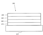
- FIG. 2 shows an inverted OLED 200.
- the device includes a substrate 210, a cathode 215, an emissive layer 220, a hole transport layer 225, and an anode 230.
- Device 200 may be fabricated by depositing the layers described, in order. Because the most common OLED configuration has a cathode disposed over the anode, and device 200 has cathode 215 disposed under anode 230, device 200 may be referred to as an "inverted" OLED. Materials similar to those described with respect to device 100 may be used in the corresponding layers of device 200.
- FIG. 2 provides one example of how some layers may be omitted from the structure of device 100.
- FIGS. 1 and 2 The simple layered structure illustrated in FIGS. 1 and 2 is provided by way of non-limiting example, and it is understood that embodiments of the invention may be used in connection with a wide variety of other structures.
- the specific materials and structures described are exemplary in nature, and other materials and structures may be used.
- Functional OLEDs may be achieved by combining the various layers described in different ways, or layers may be omitted entirely, based on design, performance, and cost factors. Other layers not specifically described may also be included. Materials other than those specifically described may be used. Although many of the examples provided herein describe various layers as comprising a single material, it is understood that combinations of materials, such as a mixture of host and dopant, or more generally a mixture, may be used. Also, the layers may have various sublayers.
- hole transport layer 225 transports holes and injects holes into emissive layer 220, and may be described as a hole transport layer or a hole injection layer.
- an OLED may be described as having an "organic layer" disposed between a cathode and an anode. This organic layer may comprise a single layer, or may further comprise multiple layers of different organic materials as described, for example, with respect to FIGS. 1 and 2 .
- OLEDs comprised of polymeric materials (PLEDs) such as disclosed in U.S. Pat. No. 5,247,190 to Friend et al. , which is incorporated by reference in its entirety.
- PLEDs polymeric materials
- OLEDs having a single organic layer may be used.
- OLEDs may be stacked, for example as described in U.S. Pat. No. 5,707,745 to Forrest et al , which is incorporated by reference in its entirety.
- the OLED structure may deviate from the simple layered structure illustrated in FIGS. 1 and 2 .
- the substrate may include an angled reflective surface to improve out-coupling, such as a mesa structure as described in U.S. Pat. No. 6,091,195 to Forrest et al. , and/or a pit structure as described in U.S. Pat. No. 5,834,893 to Bulovic et al. , which are incorporated by reference in their entireties.
- any of the layers of the various embodiments may be deposited by any suitable method.
- preferred methods include thermal evaporation, ink-jet, such as described in U.S. Pat. Nos. 6,013,982 and 6,087,196 , which are incorporated by reference in their entireties, organic vapor phase deposition (OVPD), such as described in U.S. Pat. No. 6,337,102 to Forrest et al. , which is incorporated by reference in its entirety, and deposition by organic vapor jet printing (OVJP), such as described in U.S. patent application Ser. No. 10/233,470 , which is incorporated by reference in its entirety.
- OVPD organic vapor phase deposition
- OJP organic vapor jet printing
- Other suitable deposition methods include spin coating and other solution based processes.
- Solution based processes are preferably carried out in nitrogen or an inert atmosphere.
- preferred methods include thermal evaporation.
- Preferred patterning methods include deposition through a mask, cold welding such as described in U.S. Pat. Nos. 6,294,398 and 6,468,819 , which are incorporated by reference in their entireties, and patterning associated with some of the deposition methods such as ink-jet and OVJD. Other methods may also be used.
- the materials to be deposited may be modified to make them compatible with a particular deposition method. For example, substituents such as alkyl and aryl groups, branched or unbranched, and preferably containing at least 3 carbons, may be used in small molecules to enhance their ability to undergo solution processing.
- Substituents having 20 carbons or more may be used, and 3-20 carbons is a preferred range. Materials with asymmetric structures may have better solution processibility than those having symmetric structures, because asymmetric materials may have a lower tendency to recrystallize. Dendrimer substituents may be used to enhance the ability of small molecules to undergo solution processing.
- Devices fabricated in accordance with embodiments of the invention may be incorporated into a wide variety of consumer products, including flat panel displays, computer monitors, televisions, billboards, lights for interior or exterior illumination and/or signaling, heads up displays, fully transparent displays, flexible displays, laser printers, telephones, cell phones, personal digital assistants (PDAs), laptop computers, digital cameras, camcorders, viewfinders, micro-displays, vehicles, a large area wall, theater or stadium screen, or a sign.
- PDAs personal digital assistants
- Various control mechanisms may be used to control devices fabricated in accordance with the present invention, including passive matrix and active matrix. Many of the devices are intended for use in a temperature range comfortable to humans, such as 18 degrees C. to 30 degrees C., and more preferably at room temperature (20-25 degrees C.).
- the materials and structures described herein may have applications in devices other than OLEDs.
- other optoelectronic devices such as organic solar cells and organic photodetectors may employ the materials and structures.
- organic devices such as organic transistors, may employ the materials and structures.
- halo, halogen, alkyl, cycloalkyl, alkenyl, alkynyl, arylkyl, heterocyclic group, aryl, aromatic group, and heteroaryl are known to the art, and are defined in US 7,279,704 at cols. 31-32, which are incorporated herein by reference.
- a compound comprising a heteroleptic iridium complex is provided.
- the compound is a compound of Formula I.
- R 1 , R 2 , R 3 , R 4 , R 5 , and R 6 are independently selected from the group consisting of hydrogen, deuterium, cycloalkyl, deuterated cycloalkyl, alkyl, and deuterated alkyl.
- At least one of R 1 , R 2 , R 3 , R 4 , R 5 , and R 6 is cycloalkyl, deuterated cycloalkyl, alkyl or deuterated alkyl, and any two adjacent R 1 , R 2 , R 3 , R 4 , R 5 , and R 6 are optionally linked together to form a ring.
- any of R 1 and R 2 , R 2 and R 3 , R 3 and R 4 , R 4 and R 5 , or R 5 and R 6 can be linked to form a ring.
- Ring A is attached to the 4- or 5-position of ring B.
- R and R' represent mono-, di-, tri- or tetra-substitution and are independently selected from the group consisting of: hydrogen, deuterium, halide, alkyl, cycloalkyl, heteroalkyl, arylalkyl, alkoxy, aryloxy, amino, silyl, alkenyl, cycloalkenyl, heteroalkenyl, alkynyl, aryl, heteroaryl, acyl, carbonyl, carboxylic acids, ester, nitrile, isonitrile, sulfanyl, sulfinyl, sulfonyl, phosphino, and combinations thereof.
- Ring B is numbered according to the following scheme:
- the 4-position is para to the pyridine nitrogen in ring B
- the 5-position is para to the phenyl ring attached to ring B.
- the compound is a compound of Formula II.
- the compound is a compound of Formula III.
- R 1 is alkyl.
- R 2 is alkyl.
- R 3 is alkyl.
- R 4 is alkyl.
- R 5 is alkyl.
- R 6 is alkyl.
- at least one of R 1 , R 2 , and R 3 is alkyl.
- at least one of R 4 , R 5 , and R 6 is alkyl.
- at least one of R 1 , R 2 , and R 3 is alkyl and at least one of R 4 , R 5 , and R 6 is alkyl.
- the alkyl may be replaced with a partially or fully deuterated alkyl.
- the alkyl contains at least 2 carbons, at least 3 carbons, or at most 6 carbons. Having at least 2 carbons, at least 3 carbons, or at most 6 carbons allows the compounds of Formula I to efficiently emit in the yellow portion of the spectrum, without increasing the sublimation temperature of the compounds. Increased sublimation temperatures can make it difficult to purify compounds.
- the alkyl contains greater than 10 carbons. Having an alkyl with greater than 10 carbons is useful in the solution processing of compounds of Formula I, which leads to inexpensive manufacture of OLED devices.
- the compound emits yellow light with a full width at half maximum between about 70 nm to about 110 nm when the light has a peak wavelength between about 530 nm to about 580 nm.
- FWHM full width at half maximum
- the compound is selected from the group consisting of:
- a first device comprises a first organic light-emitting device, and contains an anode, a cathode, and an organic layer, disposed between the anode and the cathode, comprising a compound having a formula of Formula I:
- R 1 , R 2 , R 3 , R 4 , R 5 , and R 6 are independently selected from the group consisting of hydrogen, deuterium, cycloalkyl, deuterated cycloalkyl, alkyl, and deuterated alkyl.
- At least one of R 1 , R 2 , R 3 , R 4 , R 5 , and R 6 is cycloalkyl, deuterated cycloalkyl, alkyl or deuterated alkyl, and any two adjacent R 1 , R 2 , R 3 , R 4 , R 5 , and R 6 are optionally linked together to form a ring.
- Ring A is attached to the 4- or 5-position of ring B.
- R and R' represent mono-, di-, tri- or tetra-substitution and are independently selected from the group consisting of: hydrogen, deuterium, halide, alkyl, cycloalkyl, heteroalkyl, arylalkyl, alkoxy, aryloxy, amino, silyl, alkenyl, cycloalkenyl, heteroalkenyl, alkynyl, aryl, heteroaryl, acyl, carbonyl, carboxylic acids, ester, nitrile, isonitrile, sulfanyl, sulfinyl, sulfonyl, phosphino, and combinations thereof.
- the organic layer is an emissive layer and the compound is an emissive dopant. In another embodiment, the organic layer is an emissive layer and the compound is a non-emissive dopant.
- the organic layer further comprises a host.
- Ar 1 and Ar 2 are independently selected from the group consisting of benzene, biphenyl, naphthalene, triphenylene, carbazole, and heteroaromatic analogs thereof, and n is from 1 to 10.
- the host has the formula:
- the host is a metal complex. Any of the metal complexes described herein are suitable hosts.
- OLEDs that incorporate compounds of Formula I have broad yellow emission profiles, as well as high quantum efficiencies and long commercial lifetimes.
- a device capable of broad yellow emission is particularly desirable in white illumination sources.
- the quality of white illumination sources can be fully described by a simple set of parameters.
- the color of the light source is given by its CIE chromaticity coordinates x and y (1931 2-degree standard observer CIE chromaticity).
- the CIE coordinates are typically represented on a two dimensional plot. Monochromatic colors fall on the perimeter of the horseshoe shaped curve starting with blue in the lower left, running through the colors of the spectrum in a clockwise direction to red in the lower right.
- the CIE coordinates of a light source of given energy and spectral shape will fall within the area of the curve. Summing light at all wavelengths uniformly gives the white or neutral point, found at the center of the diagram (CIE x,y-coordinates, 0.33, 0.33).
- Mixing light from two or more sources gives light whose color is represented by the intensity weighted average of the CIE coordinates of the independent sources. Thus, mixing light from two or more sources can be used to generate white light.
- the CIE color rendering index may be considered in addition to the CIE coordinates of the source.
- the CRI gives an indication of how well the light source will render colors of objects it illuminates.
- a perfect match of a given source to the standard illuminant gives a CRI of 100.
- a CRI value of at least 70 may be acceptable for certain applications, a preferred white light source may have a CRI of about 80 or higher.
- the compounds of Formula I have yellow emission profiles with significant red and green components.
- a blue emitter i.e. an emitter with a peak wavelength of between 400 to 500 nanometers
- OLEDs that incorporate compounds of Formula I are used for color displays (or lighting applications) using only two types of emissive compounds: a yellow emitter of Formula I and a blue emitter.
- a color display using only two emissive compounds: a broad yellow emitter of Formula I and a blue emitter may employ a color filter to selectively pass the red, green, and blue color components of a display.
- the red and green components can both come from a broad yellow emitter of Formula I.
- the first device is a consumer product. In another embodiment, the first device is an organic light-emitting device. In another aspect, the first device comprises a lighting panel.
- the first device further comprises a second emissive dopant having a peak wavelength of between 400 to 500 nanometers.
- the second emissive dopant is a fluorescent emitter.
- the second emissive dopant is a phosphorescent emitter.
- the first device further comprises a first organic light-emitting device comprising a compound of Formula I and a second light emitting device separate from the first organic light-emitting device comprising an emissive dopant having a peak wavelength of between 400 to 500 nanometers.
- the first and second light-emitting devices can be placed in any suitable spatial arrangement, depending on the needs of the desired display or lighting application.
- the first device comprises an organic-light emitting device having a first emissive layer comprising a compound of Formula I and a second emissive layer comprising an emissive dopant having a peak wavelength of between 400 to 500 nanometers.
- the first emissive layer and the second emissive layer may have one or more other layers in between them.
- All device examples were fabricated by high vacuum ( ⁇ 10 -7 Torr) thermal evaporation (VTE).
- the anode electrode is 800 ⁇ of indium tin oxide (ITO).
- the cathode consisted of 10 ⁇ of LiF followed by 1000 ⁇ of Al. All devices were encapsulated with a glass lid sealed with an epoxy resin in a nitrogen glove box ( ⁇ 1 ppm of H 2 O and O 2 ) immediately after fabrication, and a moisture getter was incorporated inside the package.
- the organic stack of the device examples consisted of sequentially, from the ITO surface, 100 ⁇ of Compound A as the hole injection layer (HIL), 300 ⁇ of 4,4'-bis[N-(1-naphthyl)-N-phenylamino]biphenyl (alpha-NPD) as the hole transporting layer (HTL), 300 ⁇ of 7 - 15 wt% of a compound of Formula I doped in with Compound H (as host) as the emissive layer (EML), 50 ⁇ or 100 ⁇ of Compound H as blocking layer (BL), 450 ⁇ or 500 of ⁇ Alq (tris-8-hydroxyquinoline aluminum) as the electron transport layer (ETL).
- HIL hole injection layer
- HTL hole transporting layer
- HTL hole transporting layer
- HTL hole transporting layer
- HTL hole transporting layer
- HTL hole transporting layer
- HTL hole transporting layer
- HTL hole transporting layer
- HTL hole transporting layer
- HTL hole
- the comparative example used 8 weight percent of Compound X in the EML.
- the device results and data are summarized in Table 1 and Table 2 from those devices.
- NPD, Alq, Compound A, Compound H, and Compound X have the following structures: TABLE 2:VTE Phosphorescent OLEDs Example HIL HTL EML (300 ⁇ , doping %) BL ETL Comparative Example 1 Compound A 100 ⁇ NPD 300 ⁇ Compound H Compound X 8% Compound H 50 ⁇ Alq 450 ⁇ Example 1 Compound A 100 ⁇ NPD 300 ⁇ Compound H Compound 3 12% Compound H 50 ⁇ Alq 450 ⁇ Example 2 Compound A 100 ⁇ NPD 300 ⁇ Compound H Compound 4 12% Compound H 50 ⁇ Alq 450 ⁇ Example 3 Compound A 100 ⁇ NPD 300 ⁇ Compound H Compound 5 10% Compound H 50 ⁇ Alq 450 ⁇ Example 4 Compound A 100 ⁇ NPD 300 ⁇ Compound 6 7% Compound H 50 ⁇ Alq 450 ⁇ Example 5 Compound A 100 ⁇ NPD 300 ⁇ Compound
- Example 1 0.435 0.550 556 84 5.9 58.3 17.3 31.3 510 Example 1 0.458 0.532 562 82 5.0 66.8 20.5 42.2 900 Example 2 0.460 0.530 562 82 5.1 61.6 19.0 38.2 1250 Example 3 0.428 0.556 552 84 5.6 77.2 22.6 43.0 630 Example 4 0.461 0.528 566 86 6.2 61.5 19.3 31.0 540 Example 5 0.485 0.508 570 84 5.0 64.6 21.2 40.4 4300 Example 6 0.462 0.528 564 82 5.7 52.4 16.2 28.9 830
- the device data show that compounds of Formula I are effective yellow emitters with broad line shape (desirable for use in white light devices), with high efficiency and commercially useful lifetimes.
- Devices made with compounds of Formula I (Examples 1-6) generally show higher luminous efficiencies (LE), external quantum efficiencies (EQE) and power efficiencies (PE) than the Comparative Example.
- L luminous efficiencies
- EQE external quantum efficiencies
- PE power efficiencies
- the alkyl substitutions reduce the aggregation of the dopant in the device, change the charge transport properties, and lead to higher efficiencies versus the Comparative Example, which lacks alkyl groups.
- Compounds 3-5, Compound 7, and Compound 8 all show lower turn-on voltages in the device than Comparative Compound X.
- the compounds of Formula I in Examples 1-6 show longer device lifetimes than the Comparative Example. For example, Compound 4 and Compound 7 had device lifetimes about 2.5 and 8 fold higher, respectively, than Comparative Compound X.
- the materials described herein as useful for a particular layer in an organic light emitting device may be used in combination with a wide variety of other materials present in the device.
- emissive dopants disclosed herein may be used in conjunction with a wide variety of hosts, transport layers, blocking layers, injection layers, electrodes and other layers that may be present.
- the materials described or referred to below are non-limiting examples of materials that may be useful in combination with the compounds disclosed herein, and one of skill in the art can readily consult the literature to identify other materials that may be useful in combination.
- a hole injecting/transporting material to be used in the present invention is not particularly limited, and any compound may be used as long as the compound is typically used as a hole injecting/transporting material.
- the material include, but not limit to: a phthalocyanine or porphryin derivative; an aromatic amine derivative; an indolocarbazole derivative; a polymer containing fluorohydrocarbon; a polymer with conductivity dopants; a conducting polymer, such as PEDOT/PSS; a self-assembly monomer derived from compounds such as phosphonic acid and sliane derivatives; a metal oxide derivative, such as MoO x ; a p-type semiconducting organic compound, such as 1,4,5,8,9,12-Hexaazatriphenylenehexacarbonitrile; a metal complex, and a cross-linkable compounds.
- aromatic amine derivatives used in HIL or HTL include, but not limit to the following general structures:
- Each of Ar 1 to Ar 9 is selected from the group consisting aromatic hydrocarbon cyclic compounds such as benzene, biphenyl, triphenyl, triphenylene, naphthalene, anthracene, phenalene, phenanthrene, fluorene, pyrene, chrysene, perylene, azulene; group consisting aromatic heterocyclic compounds such as dibenzothiophene, dibenzofuran, dibenzoselenophene, furan, thiophene, benzofuran, benzothiophene, benzoselenophene, carbazole, indolocarbazole, pyridylindole, pyrrolodipyridine, pyrazole, imidazole, triazole, oxazole, thiazole, oxadiazole, oxatriazole, dioxazole, thiadiazole, pyridine, pyridazine, pyrim
- each Ar is further substituted by a substituent selected from the group consisting of hydrogen, deuterium, halide, alkyl, cycloalkyl, heteroalkyl, arylalkyl, alkoxy, aryloxy, amino, silyl, alkenyl, cycloalkenyl, heteroalkenyl, alkynyl, aryl, heteroaryl, acyl, carbonyl, carboxylic acids, ester, nitrile, isonitrile, sulfanyl, sulfinyl, sulfonyl, phosphino, and combinations thereof.
- a substituent selected from the group consisting of hydrogen, deuterium, halide, alkyl, cycloalkyl, heteroalkyl, arylalkyl, alkoxy, aryloxy, amino, silyl, alkenyl, cycloalkenyl, heteroalkenyl, alkynyl, aryl, heteroaryl, acy
- Ar 1 to Ar 9 is independently selected from the group consisting of:
- k is an integer from 1 to 20; X 1 to X 8 is C (including CH) or N; Ar 1 has the same group defined above.
- metal complexes used in HIL or HTL include, but not limit to the following general formula:
- M is a metal, having an atomic weight greater than 40;
- (Y 1 -Y 2 ) is a bidentate ligand, Y and Y 2 are independently selected from C, N, O, P, and S;
- L is an ancillary ligand;
- m is an integer value from 1 to the maximum number of ligands that may be attached to the metal; and m+n is the maximum number of ligands that may be attached to the metal.
- (Y 1 -Y 2 ) is a 2-phenylpyridine derivative.
- (Y 1 -Y 2 ) is a carbene ligand.
- M is selected from Ir, Pt, Os, and Zn.
- the metal complex has a smallest oxidation potential in solution vs. Fc + /Fc couple less than about 0.6 V.
- the light emitting layer of the organic EL device of the present invention preferably contains at least a metal complex as light emitting material, and may contain a host material using the metal complex as a dopant material.
- the host material are not particularly limited, and any metal complexes or organic compounds may be used as long as the triplet energy of the host is larger than that of the dopant.
- metal complexes used as host are preferred to have the following general formula:
- M is a metal
- (Y 3 -Y 4 ) is a bidentate ligand, Y 3 and Y 4 are independently selected from C, N, O, P, and S
- L is an ancillary ligand
- m is an integer value from 1 to the maximum number of ligands that may be attached to the metal
- m+n is the maximum number of ligands that may be attached to the metal.
- the metal complexes are:
- (O-N) is a bidentate ligand, having metal coordinated to atoms O and N.
- M is selected from Ir and Pt.
- (Y 3 -Y 4 ) is a carbene ligand.
- organic compounds used as host are selected from the group consisting aromatic hydrocarbon cyclic compounds such as benzene, biphenyl, triphenyl, triphenylene, naphthalene, anthracene, phenalene, phenanthrene, fluorene, pyrene, chrysene, perylene, azulene; group consisting aromatic heterocyclic compounds such as dibenzothiophene, dibenzofuran, dibenzoselenophene, furan, thiophene, benzofuran, benzothiophene, benzoselenophene, carbazole, indolocarbazole, pyridylindole, pyrrolodipyridine, pyrazole, imidazole, triazole, oxazole, thiazole, oxadiazole, oxatriazole, dioxazole, thiadiazole, pyridine, pyridazine, pyrimidine
- each group is further substituted by a substituent selected from the group consisting of hydrogen, deuterium, halide, alkyl, cycloalkyl, heteroalkyl, arylalkyl, alkoxy, aryloxy, amino, silyl, alkenyl, cycloalkenyl, heteroalkenyl, alkynyl, aryl, heteroaryl, acyl, carbonyl, carboxylic acids, ester, nitrile, isonitrile, sulfanyl, sulfinyl, sulfonyl, phosphino, and combinations thereof.
- a substituent selected from the group consisting of hydrogen, deuterium, halide, alkyl, cycloalkyl, heteroalkyl, arylalkyl, alkoxy, aryloxy, amino, silyl, alkenyl, cycloalkenyl, heteroalkenyl, alkynyl, aryl, heteroaryl, acy
- host compound contains at least one of the following groups in the molecule:
- R 1 to R 7 is independently selected from the group consisting of hydrogen, alkyl, alkoxy, amino, alkenyl, alkynyl, arylalkyl, heteroalkyl, aryl and heteroaryl, when it is aryl or heteroaryl, it has the similar definition as Ar's mentioned above.
- k is an integer from 0 to 20.
- X 1 to X 8 is selected from C (including CH) or N.
- a hole blocking layer may be used to reduce the number of holes and/or excitons that leave the emissive layer.
- the presence of such a blocking layer in a device may result in substantially higher efficiencies as compared to a similar device lacking a blocking layer.
- a blocking layer may be used to confine emission to a desired region of an OLED.
- compound used in HBL contains the same molecule used as host described above.
- compound used in HBL contains at least one of the following groups in the molecule:
- Electron transport layer may include a material capable of transporting electrons. Electron transport layer may be intrinsic (undoped), or doped. Doping may be used to enhance conductivity. Examples of the ETL material are not particularly limited, and any metal complexes or organic compounds may be used as long as they are typically used to transport electrons.
- compound used in ETL contains at least one of the following groups in the molecule:
- R 1 is selected from the group consisting of hydrogen, alkyl, alkoxy, amino, alkenyl, alkynyl, arylalkyl, heteroalkyl, aryl and heteroaryl, when it is aryl or heteroaryl, it has the similar definition as Ar's mentioned above.
- Ar 1 to Ar 3 has the similar definition as Ar's mentioned above.
- k is an integer from 0 to 20.
- X 1 to X 8 is selected from C (including CH) or N.
- the metal complexes used in ETL contains, but not limit to the following general formula:
- (O-N) or (N-N) is a bidentate ligand, having metal coordinated to atoms O, N or N, N; L is an ancillary ligand; m is an integer value from 1 to the maximum number of ligands that may be attached to the metal.
- the hydrogen atoms can be partially or fully deuterated.
- hole injection materials In addition to and / or in combination with the materials disclosed herein, many hole injection materials, hole transporting materials, host materials, dopant materials, exiton/hole blocking layer materials, electron transporting and electron injecting materials may be used in an OLED.
- Non-limiting examples of the materials that may be used in an OLED in combination with materials disclosed herein are listed in Table 3 below. Table 3 lists non-limiting classes of materials, non-limiting examples of compounds for each class, and references that disclose the materials. TABLE 3 MATERIAL EXAMPLES OF MATERIAL PUBLICATIONS Hole injection materials Phthalocyanine and porphryin compounds Appl. Phys. Lett. 69, 2160 (1996 ) Starburst triarylamines J. Lumin.
- Cy is cyclohexyl
- dba is dibenzylideneacetone
- EtOAc is ethyl acetate
- S-Phos is dicyclohexyl(2',6'-dimethoxy-[1,1'-biphenyl]-3-yl)phosphine
- THF is tetrahydrofuran
- DCM is dichloromethane
- PPh 3 triphenylphosphine.
- iridium trifluoromethanesulfonate salt The iridium dimer (11 g, 9.75 mmol), as obtained in Step 2 above, was suspended in 600 mL of dichloromethane. In a separate flask, silver(I) trifluoromethanesulfonate (5.26 g, 20.48 mmol) was dissolved in MeOH (300 mL) and added slowly to the dichloromethane suspension with continuous stirring at room temperature. The reaction mixture was stirred overnight in the dark. The reaction mixture was filtered through a tightly packed Celite® bed and the solvent was removed under vacuum to give 15 g (100% yield) of product as a brownish green solid. The product was used without further purification.
- the crude product was adsorbed on Celite® for column chromatography.
- the crude product was chromatographed on silica gel with 10% EtOAc in hexane to yield 10 g (75% yield) of the desired product (HPLC purity: 99.8%).
- the product was confirmed by GC/MS.
- iridium trifluoromethanesulfonate salt The iridium dimer (6.2 g, 4.94 mmol), obtained as in Step 4 above, was dissolved in 500 mL of dichloromethane. In a separate flask, silver(I) trifluoromethanesulfonate (2.66 g, 10.37 mmol) was dissolved in MeOH (250 mL) and added slowly to the dichloromethane solution with continuous stirring at room temperature. The reaction mixture was stirred overnight in the dark. The reaction mixture was filtered through a tightly packed Celite® bed and the solvent was removed under vacuum to give 7.8 g (100% yield) of product as a brownish green solid. The product was used without further purification.
- the reaction mixture was degassed with N 2 for 20 minutes, then 4,4,5,5-tetramethyl-2-(prop-1-en-2-yl)-1,3,2-dioxaborolane (12.07 mL, 64.2 mmol) and Pd 2 (dba) 3 (0.980 g, 1.070 mmol) were added and the reaction mixture was refluxed for 18 h. The aqueous layer was removed and the organic layer was concentrated to dryness. The crude product was chromatographed on silica gel with 0 - 20% EtOAc in hexane to yield 11 g of the desired product (HPLC purity: 95%). The product was confirmed by GC/MS.
- irdium trifluoromethanesulfonate salt The iridium dimer (5.3 g, 4.27 mmol) was dissolved in 500 mL of dichloromethane. In a separate flask, silver(I) trifluoromethanesulfonate (2.3 g, 8.97 mmol) was dissolved in MeOH (250 mL) and added slowly to the dichloromethane solution with continuous stirring at room temperature. The reaction mixture was stirred overnight in the dark. The reaction mixture was filtered through a tightly packed Celite® bed and the solvent was removed under vacuum to give 6.9 g (100% yield) of product as a brownish solid. The product was used without further purification.
Abstract
Description
- This application claims priority to
U.S. Application No. 61/572,276, filed May 27, 2011 - The claimed invention was made by, on behalf of, and/or in connection with one or more of the following parties to a joint university corporation research agreement: Regents of the University of Michigan, Princeton University, The University of Southern California, and the Universal Display Corporation. The agreement was in effect on and before the date the claimed invention was made, and the claimed invention was made as a result of activities undertaken within the scope of the agreement.
- The present invention relates to heteroleptic iridium complexes containing phenylpyridine ligands. These heteroleptic iridium complexes are useful as dopants in OLED devices.
- Opto-electronic devices that make use of organic materials are becoming increasingly desirable for a number of reasons. Many of the materials used to make such devices are relatively inexpensive, so organic opto-electronic devices have the potential for cost advantages over inorganic devices. In addition, the inherent properties of organic materials, such as their flexibility, may make them well suited for particular applications such as fabrication on a flexible substrate. Examples of organic opto-electronic devices include organic light emitting devices (OLEDs), organic phototransistors, organic photovoltaic cells, and organic photodetectors. For OLEDs, the organic materials may have performance advantages over conventional materials. For example, the wavelength at which an organic emissive layer emits light may generally be readily tuned with appropriate dopants.
- OLEDs make use of thin organic films that emit light when voltage is applied across the device. OLEDs are becoming an increasingly interesting technology for use in applications such as flat panel displays, illumination, and backlighting. Several OLED materials and configurations are described in
U.S. Pat. Nos. 5,844,363 ,6,303,238 , and5,707,745 , which are incorporated herein by reference in their entirety. - One application for phosphorescent emissive molecules is a full color display. Industry standards for such a display call for pixels adapted to emit particular colors, referred to as "saturated" colors. In particular, these standards call for saturated red, green, and blue pixels. Color may be measured using CIE coordinates, which are well known to the art.
- One example of a green emissive molecule is tris(2-phenylpyridine) iridium, denoted Ir(ppy)3, which has the following structure:

- In this, and later figures herein, we depict the dative bond from nitrogen to metal (here, Ir) as a straight line.
- As used herein, the term "organic" includes polymeric materials as well as small molecule organic materials that may be used to fabricate organic opto-electronic devices. "Small molecule" refers to any organic material that is not a polymer, and "small molecules" may actually be quite large. Small molecules may include repeat units in some circumstances. For example, using a long chain alkyl group as a substituent does not remove a molecule from the "small molecule" class. Small molecules may also be incorporated into polymers, for example as a pendent group on a polymer backbone or as a part of the backbone. Small molecules may also serve as the core moiety of a dendrimer, which consists of a series of chemical shells built on the core moiety. The core moiety of a dendrimer may be a fluorescent or phosphorescent small molecule emitter. A dendrimer may be a "small molecule," and it is believed that all dendrimers currently used in the field of OLEDs are small molecules.
- As used herein, "top" means furthest away from the substrate, while "bottom" means closest to the substrate. Where a first layer is described as "disposed over" a second layer, the first layer is disposed further away from substrate. There may be other layers between the first and second layer, unless it is specified that the first layer is "in contact with" the second layer. For example, a cathode may be described as "disposed over" an anode, even though there are various organic layers in between.
- As used herein, "solution processible" means capable of being dissolved, dispersed, or transported in and/or deposited from a liquid medium, either in solution or suspension form.
- A ligand may be referred to as "photoactive" when it is believed that the ligand directly contributes to the photoactive properties of an emissive material. A ligand may be referred to as "ancillary" when it is believed that the ligand does not contribute to the photoactive properties of an emissive material, although an ancillary ligand may alter the properties of a photoactive ligand.
- As used herein, and as would be generally understood by one skilled in the art, a first "Highest Occupied Molecular Orbital" (HOMO) or "Lowest Unoccupied Molecular Orbital" (LUMO) energy level is "greater than" or "higher than" a second HOMO or LUMO energy level if the first energy level is closer to the vacuum energy level. Since ionization potentials (IP) are measured as a negative energy relative to a vacuum level, a higher HOMO energy level corresponds to an IP having a smaller absolute value (an IP that is less negative). Similarly, a higher LUMO energy level corresponds to an electron affinity (EA) having a smaller absolute value (an EA that is less negative). On a conventional energy level diagram, with the vacuum level at the top, the LUMO energy level of a material is higher than the HOMO energy level of the same material. A "higher" HOMO or LUMO energy level appears closer to the top of such a diagram than a "lower" HOMO or LUMO energy level.
- As used herein, and as would be generally understood by one skilled in the art, a first work function is "greater than" or "higher than" a second work function if the first work function has a higher absolute value. Because work functions are generally measured as negative numbers relative to vacuum level, this means that a "higher" work function is more negative. On a conventional energy level diagram, with the vacuum level at the top, a "higher" work function is illustrated as further away from the vacuum level in the downward direction. Thus, the definitions of HOMO and LUMO energy levels follow a different convention than work functions.
- More details on OLEDs, and the definitions described above, can be found in
US Pat. No. 7,279,704 , which is incorporated herein by reference in its entirety. - A compound comprising a heteroleptic iridium complex is provided. In one aspect, the compound is a compound of Formula I.

- In one aspect, the compound is a compound of Formula II.

- In another aspect, the compound is a compound of Formula III.

- In one aspect, R1 is alkyl. In one aspect, R2 is alkyl. In one aspect, R3 is alkyl. In one aspect, R4 is alkyl. In one aspect, R5 is alkyl. In one aspect, R6 is alkyl. In one aspect, at least one of R1, R2, and R3 is alkyl. In one aspect, at least one of R4, R5, and R6 is alkyl. In another aspect, at least one of R1, R2, and R3 is alkyl and at least one of R4, R5, and R6 is alkyl.
- In one aspect, the alkyl contains at least 2 carbons, at least 3 carbons, or at most 6 carbons. In another aspect, the alkyl contains greater than 10 carbons.
- In one aspect, the compound emits yellow light with a full width at half maximum between about 70 nm to about 110 nm when the light has a peak wavelength between about 530 nm to about 580 nm.
- Specific non-limiting compounds are provided. In one aspect, the compound is selected from Compound 1 - Compound 89.
- In one aspect a first device is provided. The first device comprises a first organic light emitting device, and contains an anode, a cathode, and an organic layer, disposed between the anode and the cathode, comprising a compound having a formula of Formula I:

- In one aspect, the organic layer is an emissive layer and the compound is an emissive dopant. In another aspect, the organic layer is an emissive layer and the compound is an non-emissive dopant.
- In another aspect, the organic layer further comprises a host. In one aspect, the host comprises a triphenylene containing benzo-fused thiophene or benzo-fused furan, wherein any substituent in the host is an unfused substituent independently selected from the group consisting of CnH2n+1, OCnH2n+1, OAr1, N(CnH2n+1)2, N(Ar1)(Ar2), CH=CH-CnH2n+1, C≡CHCnH2n+1, Ar1, Ar1-Ar2, CnH2n-Ar1, or no substitution. Ar1 and Ar2 are independently selected from the group consisting of benzene, biphenyl, naphthalene, triphenylene, carbazole, and heteroaromatic analogs thereof, and n is from 1 to 10. In one aspect, the host has the formula:

- In one aspect, the host is a metal complex.
- In one aspect, the first device is a consumer product. In another aspect, the first device is an organic light-emitting device. In another aspect, the first device comprises a lighting panel.
- In one aspect, the first device further comprises a second emissive dopant having a peak wavelength of between 400 to 500 nanometers. In one aspect, the second emissive dopant is a fluorescent emitter. In another aspect, the second emissive dopant is a phosphorescent emitter.
- In one aspect, the first device further comprises a first organic light-emitting device comprising a compound of Formula I and a second light emitting device separate from the first organic light-emitting device comprising an emissive dopant having a peak wavelength of between 400 to 500 nanometers. In another aspect, the first device comprises an organic-light emitting device having a first emissive layer compring a compound of Formula I and a second emissive layer comprising an emissive dopant having a peak wavelength of between 400 to 500 nanometers.
-
-
FIG. 1 shows an organic light emitting device. -
FIG. 2 shows an inverted organic light emitting device that does not have a separate electron transport layer. -
FIG. 3 shows a compound of Formula I. - Generally, an OLED comprises at least one organic layer disposed between and electrically connected to an anode and a cathode. When a current is applied, the anode injects holes and the cathode injects electrons into the organic layer(s). The injected holes and electrons each migrate toward the oppositely charged electrode. When an electron and hole localize on the same molecule, an "exciton," which is a localized electron-hole pair having an excited energy state, is formed. Light is emitted when the exciton relaxes via a photoemissive mechanism. In some cases, the exciton may be localized on an excimer or an exciplex. Non-radiative mechanisms, such as thermal relaxation, may also occur, but are generally considered undesirable.
- The initial OLEDs used emissive molecules that emitted light from their singlet states ("fluorescence") as disclosed, for example, in
U.S. Pat. No. 4,769,292 , which is incorporated by reference in its entirety. Fluorescent emission generally occurs in a time frame of less than 10 nanoseconds. - More recently, OLEDs having emissive materials that emit light from triplet states ("phosphorescence") have been demonstrated. Baldo et al., "Highly Efficient Phosphorescent Emission from Organic Electroluminescent Devices," Nature, vol. 395, 151-154, 1998; ("Baldo-I") and Baldo et al., "Very high-efficiency green organic light-emitting devices based on electrophosphorescence," Appl. Phys. Lett., vol. 75, No. 3, 4-6 (1999) ("Baldo-II"), which are incorporated by reference in their entireties. Phosphorescence is described in more detail in
US Pat. No. 7,279,704 at cols. 5-6, which are incorporated by reference. -
FIG. 1 shows an organiclight emitting device 100. The figures are not necessarily drawn to scale.Device 100 may include asubstrate 110, ananode 115, ahole injection layer 120, ahole transport layer 125, anelectron blocking layer 130, anemissive layer 135, ahole blocking layer 140, anelectron transport layer 145, anelectron injection layer 150, aprotective layer 155, and acathode 160.Cathode 160 is a compound cathode having a firstconductive layer 162 and a secondconductive layer 164.Device 100 may be fabricated by depositing the layers described, in order. The properties and functions of these various layers, as well as example materials, are described in more detail inUS 7,279,704 at cols. 6-10, which are incorporated by reference. - More examples for each of these layers are available. For example, a flexible and transparent substrate-anode combination is disclosed in
U.S. Pat. No. 5,844,363 , which is incorporated by reference in its entirety. An example of a p-doped hole transport layer is m-MTDATA doped with F.sub.4-TCNQ at a molar ratio of 50:1, as disclosed inU.S. Patent Application Publication No. 2003/0230980 , which is incorporated by reference in its entirety. Examples of emissive and host materials are disclosed inU.S. Pat. No. 6,303,238 to Thompson et al. , which is incorporated by reference in its entirety. An example of an n-doped electron transport layer is BPhen doped with Li at a molar ratio of 1:1, as disclosed inU.S. Patent Application Publication No. 2003/0230980 , which is incorporated by reference in its entirety.U.S. Pat. Nos. 5,703,436 and5,707,745 , which are incorporated by reference in their entireties, disclose examples of cathodes including compound cathodes having a thin layer of metal such as Mg:Ag with an overlying transparent, electrically-conductive, sputter-deposited ITO layer. The theory and use of blocking layers is described in more detail inU.S. Pat. No. 6,097,147 andU.S. Patent Application Publication No. 2003/0230980 , which are incorporated by reference in their entireties. Examples of injection layers are provided inU.S. Patent Application Publication No. 2004/0174116 , which is incorporated by reference in its entirety. A description of protective layers may be found inU.S. Patent Application Publication No. 2004/0174116 , which is incorporated by reference in its entirety. -
FIG. 2 shows aninverted OLED 200. The device includes asubstrate 210, acathode 215, anemissive layer 220, ahole transport layer 225, and ananode 230.Device 200 may be fabricated by depositing the layers described, in order. Because the most common OLED configuration has a cathode disposed over the anode, anddevice 200 hascathode 215 disposed underanode 230,device 200 may be referred to as an "inverted" OLED. Materials similar to those described with respect todevice 100 may be used in the corresponding layers ofdevice 200.FIG. 2 provides one example of how some layers may be omitted from the structure ofdevice 100. - The simple layered structure illustrated in
FIGS. 1 and2 is provided by way of non-limiting example, and it is understood that embodiments of the invention may be used in connection with a wide variety of other structures. The specific materials and structures described are exemplary in nature, and other materials and structures may be used. Functional OLEDs may be achieved by combining the various layers described in different ways, or layers may be omitted entirely, based on design, performance, and cost factors. Other layers not specifically described may also be included. Materials other than those specifically described may be used. Although many of the examples provided herein describe various layers as comprising a single material, it is understood that combinations of materials, such as a mixture of host and dopant, or more generally a mixture, may be used. Also, the layers may have various sublayers. The names given to the various layers herein are not intended to be strictly limiting. For example, indevice 200,hole transport layer 225 transports holes and injects holes intoemissive layer 220, and may be described as a hole transport layer or a hole injection layer. In one embodiment, an OLED may be described as having an "organic layer" disposed between a cathode and an anode. This organic layer may comprise a single layer, or may further comprise multiple layers of different organic materials as described, for example, with respect toFIGS. 1 and2 . - Structures and materials not specifically described may also be used, such as OLEDs comprised of polymeric materials (PLEDs) such as disclosed in
U.S. Pat. No. 5,247,190 to Friend et al. , which is incorporated by reference in its entirety. By way of further example, OLEDs having a single organic layer may be used. OLEDs may be stacked, for example as described inU.S. Pat. No. 5,707,745 to Forrest et al , which is incorporated by reference in its entirety. The OLED structure may deviate from the simple layered structure illustrated inFIGS. 1 and2 . For example, the substrate may include an angled reflective surface to improve out-coupling, such as a mesa structure as described inU.S. Pat. No. 6,091,195 to Forrest et al. , and/or a pit structure as described inU.S. Pat. No. 5,834,893 to Bulovic et al. , which are incorporated by reference in their entireties. - Unless otherwise specified, any of the layers of the various embodiments may be deposited by any suitable method. For the organic layers, preferred methods include thermal evaporation, ink-jet, such as described in
U.S. Pat. Nos. 6,013,982 and6,087,196 , which are incorporated by reference in their entireties, organic vapor phase deposition (OVPD), such as described inU.S. Pat. No. 6,337,102 to Forrest et al. , which is incorporated by reference in its entirety, and deposition by organic vapor jet printing (OVJP), such as described inU.S. patent application Ser. No. 10/233,470 , which is incorporated by reference in its entirety. Other suitable deposition methods include spin coating and other solution based processes. Solution based processes are preferably carried out in nitrogen or an inert atmosphere. For the other layers, preferred methods include thermal evaporation. Preferred patterning methods include deposition through a mask, cold welding such as described inU.S. Pat. Nos. 6,294,398 and6,468,819 , which are incorporated by reference in their entireties, and patterning associated with some of the deposition methods such as ink-jet and OVJD. Other methods may also be used. The materials to be deposited may be modified to make them compatible with a particular deposition method. For example, substituents such as alkyl and aryl groups, branched or unbranched, and preferably containing at least 3 carbons, may be used in small molecules to enhance their ability to undergo solution processing. Substituents having 20 carbons or more may be used, and 3-20 carbons is a preferred range. Materials with asymmetric structures may have better solution processibility than those having symmetric structures, because asymmetric materials may have a lower tendency to recrystallize. Dendrimer substituents may be used to enhance the ability of small molecules to undergo solution processing. - Devices fabricated in accordance with embodiments of the invention may be incorporated into a wide variety of consumer products, including flat panel displays, computer monitors, televisions, billboards, lights for interior or exterior illumination and/or signaling, heads up displays, fully transparent displays, flexible displays, laser printers, telephones, cell phones, personal digital assistants (PDAs), laptop computers, digital cameras, camcorders, viewfinders, micro-displays, vehicles, a large area wall, theater or stadium screen, or a sign. Various control mechanisms may be used to control devices fabricated in accordance with the present invention, including passive matrix and active matrix. Many of the devices are intended for use in a temperature range comfortable to humans, such as 18 degrees C. to 30 degrees C., and more preferably at room temperature (20-25 degrees C.).
- The materials and structures described herein may have applications in devices other than OLEDs. For example, other optoelectronic devices such as organic solar cells and organic photodetectors may employ the materials and structures. More generally, organic devices, such as organic transistors, may employ the materials and structures.
- The terms halo, halogen, alkyl, cycloalkyl, alkenyl, alkynyl, arylkyl, heterocyclic group, aryl, aromatic group, and heteroaryl are known to the art, and are defined in
US 7,279,704 at cols. 31-32, which are incorporated herein by reference. - A compound comprising a heteroleptic iridium complex is provided. In one embodiment, the compound is a compound of Formula I.

- Ring B is numbered according to the following scheme:

- In one embodiment, the compound is a compound of Formula II.

- In another embodiment, the compound is a compound of Formula III.

- In one embodiment, R1 is alkyl. In one embodiment, R2 is alkyl. In one embodiment, R3 is alkyl. In one embodiment, R4 is alkyl. In one embodiment, R5 is alkyl. In one embodiment, R6 is alkyl. In one embodiment, at least one of R1, R2, and R3 is alkyl. In one embodiment, at least one of R4, R5, and R6 is alkyl. In another embodiment, at least one of R1, R2, and R3 is alkyl and at least one of R4, R5, and R6 is alkyl. In any of the foregoing embodiments, the alkyl may be replaced with a partially or fully deuterated alkyl.
- In one embodiment, the alkyl contains at least 2 carbons, at least 3 carbons, or at most 6 carbons. Having at least 2 carbons, at least 3 carbons, or at most 6 carbons allows the compounds of Formula I to efficiently emit in the yellow portion of the spectrum, without increasing the sublimation temperature of the compounds. Increased sublimation temperatures can make it difficult to purify compounds. In another embodiment, the alkyl contains greater than 10 carbons. Having an alkyl with greater than 10 carbons is useful in the solution processing of compounds of Formula I, which leads to inexpensive manufacture of OLED devices.
- In one embodiment, the compound emits yellow light with a full width at half maximum between about 70 nm to about 110 nm when the light has a peak wavelength between about 530 nm to about 580 nm. When compounds of Formula I have the above range of full width at half maximum (FWHM) with the accompanying range of peak wavelengths, they are efficient yellow emitters with broad line shapes, which is desirable in white light applications.
- Specific non-limiting compounds are provided. In one embodiment, the compound is selected from the group consisting of:


- In one embodiment a first device is provided. The first device comprises a first organic light-emitting device, and contains an anode, a cathode, and an organic layer, disposed between the anode and the cathode, comprising a compound having a formula of Formula I:

- In one embodiment, the organic layer is an emissive layer and the compound is an emissive dopant. In another embodiment, the organic layer is an emissive layer and the compound is a non-emissive dopant.
- In another embodiment, the organic layer further comprises a host. In one embodiment, the host comprises a triphenylene containing benzo-fused thiophene or benzo-fused furan, wherein any substituent in the host is an unfused substituent independently selected from the group consisting of CnH2n+1, OCnH2n+1, OAr1, N(CnH2n+1)2, N(Ar1)(Ar2), CH=CH-CnH2n+1, C≡CHCnH2n+1, Ar1, Ar1-Ar2, CnH2n-Ar1, or no substitution. Ar1 and Ar2 are independently selected from the group consisting of benzene, biphenyl, naphthalene, triphenylene, carbazole, and heteroaromatic analogs thereof, and n is from 1 to 10. In one embodiment, the host has the formula:

- In one embodiment, the host is a metal complex. Any of the metal complexes described herein are suitable hosts.
- OLEDs that incorporate compounds of Formula I have broad yellow emission profiles, as well as high quantum efficiencies and long commercial lifetimes. A device capable of broad yellow emission is particularly desirable in white illumination sources.
- The quality of white illumination sources can be fully described by a simple set of parameters. The color of the light source is given by its CIE chromaticity coordinates x and y (1931 2-degree standard observer CIE chromaticity). The CIE coordinates are typically represented on a two dimensional plot. Monochromatic colors fall on the perimeter of the horseshoe shaped curve starting with blue in the lower left, running through the colors of the spectrum in a clockwise direction to red in the lower right. The CIE coordinates of a light source of given energy and spectral shape will fall within the area of the curve. Summing light at all wavelengths uniformly gives the white or neutral point, found at the center of the diagram (CIE x,y-coordinates, 0.33, 0.33). Mixing light from two or more sources gives light whose color is represented by the intensity weighted average of the CIE coordinates of the independent sources. Thus, mixing light from two or more sources can be used to generate white light.
- When considering the use of these white light sources for illumination, the CIE color rendering index (CRI) may be considered in addition to the CIE coordinates of the source. The CRI gives an indication of how well the light source will render colors of objects it illuminates. A perfect match of a given source to the standard illuminant gives a CRI of 100. Though a CRI value of at least 70 may be acceptable for certain applications, a preferred white light source may have a CRI of about 80 or higher.
- The compounds of Formula I have yellow emission profiles with significant red and green components. The addition of a blue emitter, i.e. an emitter with a peak wavelength of between 400 to 500 nanometers, together with appropriate filters on OLEDs incorporating the compound of Formula I allows for the reproduction of the RGB spectrum. In some embodiments, OLEDs that incorporate compounds of Formula I are used for color displays (or lighting applications) using only two types of emissive compounds: a yellow emitter of Formula I and a blue emitter. A color display using only two emissive compounds: a broad yellow emitter of Formula I and a blue emitter, may employ a color filter to selectively pass the red, green, and blue color components of a display. The red and green components can both come from a broad yellow emitter of Formula I.
- In one embodiment, the first device is a consumer product. In another embodiment, the first device is an organic light-emitting device. In another aspect, the first device comprises a lighting panel.
- In one embodiment, the first device further comprises a second emissive dopant having a peak wavelength of between 400 to 500 nanometers. In one embodiment, the second emissive dopant is a fluorescent emitter. In another embodiment, the second emissive dopant is a phosphorescent emitter.
- In one embodiment, the first device further comprises a first organic light-emitting device comprising a compound of Formula I and a second light emitting device separate from the first organic light-emitting device comprising an emissive dopant having a peak wavelength of between 400 to 500 nanometers. The first and second light-emitting devices can be placed in any suitable spatial arrangement, depending on the needs of the desired display or lighting application.
- In another embodiment, the first device comprises an organic-light emitting device having a first emissive layer comprising a compound of Formula I and a second emissive layer comprising an emissive dopant having a peak wavelength of between 400 to 500 nanometers. The first emissive layer and the second emissive layer may have one or more other layers in between them.
- All device examples were fabricated by high vacuum (<10-7 Torr) thermal evaporation (VTE). The anode electrode is 800Å of indium tin oxide (ITO). The cathode consisted of 10 Å of LiF followed by 1000 Å of Al. All devices were encapsulated with a glass lid sealed with an epoxy resin in a nitrogen glove box (<1 ppm of H2O and O2) immediately after fabrication, and a moisture getter was incorporated inside the package.
- The organic stack of the device examples consisted of sequentially, from the ITO surface, 100 Å of Compound A as the hole injection layer (HIL), 300 Å of 4,4'-bis[N-(1-naphthyl)-N-phenylamino]biphenyl (alpha-NPD) as the hole transporting layer (HTL), 300 Å of 7 - 15 wt% of a compound of Formula I doped in with Compound H (as host) as the emissive layer (EML), 50 Å or 100 Å of Compound H as blocking layer (BL), 450 Å or 500 of Å Alq (tris-8-hydroxyquinoline aluminum) as the electron transport layer (ETL). The comparative example used 8 weight percent of Compound X in the EML. The device results and data are summarized in Table 1 and Table 2 from those devices. As used herein, NPD, Alq, Compound A, Compound H, and Compound X have the following structures:


TABLE 2:VTE Phosphorescent OLEDs Example HIL HTL EML (300 Å, doping %) BL ETL Comparative Example 1 Compound A 100Å NPD 300Å Compound H Compound X 8% Compound H 50Å Alq 450Å Example 1 Compound A 100Å NPD 300Å Compound H Compound 3 12% Compound H 50Å Alq 450Å Example 2 Compound A 100Å NPD 300Å Compound H Compound 4 12% Compound H 50Å Alq 450Å Example 3 Compound A 100Å NPD 300Å Compound H Compound 5 10% Compound H 50Å Alq 450Å Example 4 Compound A 100Å NPD 300Å Compound H Compound 6 7% Compound H 50Å Alq 450Å Example 5 Compound A 100Å NPD 300Å Compound H Compound 7 10% Compound H 50Å Alq 500Å Example 6 Compound A 100Å NPD 300Å Compound H Compound 8 7% Compound H 50Å Alq 450Å TABLE 3. VTE Device Data Example x y λmax FWH M (nm) Voltage (V) LE (Cd/A) EQE (%) PE (lm/W) LT80% (h) Comparative Example 1 0.435 0.550 556 84 5.9 58.3 17.3 31.3 510 Example 1 0.458 0.532 562 82 5.0 66.8 20.5 42.2 900 Example 2 0.460 0.530 562 82 5.1 61.6 19.0 38.2 1250 Example 3 0.428 0.556 552 84 5.6 77.2 22.6 43.0 630 Example 4 0.461 0.528 566 86 6.2 61.5 19.3 31.0 540 Example 5 0.485 0.508 570 84 5.0 64.6 21.2 40.4 4300 Example 6 0.462 0.528 564 82 5.7 52.4 16.2 28.9 830 - The device data show that compounds of Formula I are effective yellow emitters with broad line shape (desirable for use in white light devices), with high efficiency and commercially useful lifetimes. Devices made with compounds of Formula I (Examples 1-6) generally show higher luminous efficiencies (LE), external quantum efficiencies (EQE) and power efficiencies (PE) than the Comparative Example. Without being bound by theory, it is believed that the alkyl substitutions reduce the aggregation of the dopant in the device, change the charge transport properties, and lead to higher efficiencies versus the Comparative Example, which lacks alkyl groups. Additionally, Compounds 3-5, Compound 7, and Compound 8 all show lower turn-on voltages in the device than Comparative Compound X. Finally, the compounds of Formula I in Examples 1-6 show longer device lifetimes than the Comparative Example. For example, Compound 4 and Compound 7 had device lifetimes about 2.5 and 8 fold higher, respectively, than Comparative Compound X.
- The materials described herein as useful for a particular layer in an organic light emitting device may be used in combination with a wide variety of other materials present in the device. For example, emissive dopants disclosed herein may be used in conjunction with a wide variety of hosts, transport layers, blocking layers, injection layers, electrodes and other layers that may be present. The materials described or referred to below are non-limiting examples of materials that may be useful in combination with the compounds disclosed herein, and one of skill in the art can readily consult the literature to identify other materials that may be useful in combination.
- A hole injecting/transporting material to be used in the present invention is not particularly limited, and any compound may be used as long as the compound is typically used as a hole injecting/transporting material. Examples of the material include, but not limit to: a phthalocyanine or porphryin derivative; an aromatic amine derivative; an indolocarbazole derivative; a polymer containing fluorohydrocarbon; a polymer with conductivity dopants; a conducting polymer, such as PEDOT/PSS; a self-assembly monomer derived from compounds such as phosphonic acid and sliane derivatives; a metal oxide derivative, such as MoOx; a p-type semiconducting organic compound, such as 1,4,5,8,9,12-Hexaazatriphenylenehexacarbonitrile; a metal complex, and a cross-linkable compounds.
- Examples of aromatic amine derivatives used in HIL or HTL include, but not limit to the following general structures:


- Each of Ar1 to Ar9 is selected from the group consisting aromatic hydrocarbon cyclic compounds such as benzene, biphenyl, triphenyl, triphenylene, naphthalene, anthracene, phenalene, phenanthrene, fluorene, pyrene, chrysene, perylene, azulene; group consisting aromatic heterocyclic compounds such as dibenzothiophene, dibenzofuran, dibenzoselenophene, furan, thiophene, benzofuran, benzothiophene, benzoselenophene, carbazole, indolocarbazole, pyridylindole, pyrrolodipyridine, pyrazole, imidazole, triazole, oxazole, thiazole, oxadiazole, oxatriazole, dioxazole, thiadiazole, pyridine, pyridazine, pyrimidine, pyrazine, triazine, oxazine, oxathiazine, oxadiazine, indole, benzimidazole, indazole, indoxazine, benzoxazole, benzisoxazole, benzothiazole, quinoline, isoquinoline, cinnoline, quinazoline, quinoxaline, naphthyridine, phthalazine, pteridine, xanthene, acridine, phenazine, phenothiazine, phenoxazine, benzofuropyridine, furodipyridine, benzothienopyridine, thienodipyridine, benzoselenophenopyridine, and selenophenodipyridine; and group consisting 2 to 10 cyclic structural units which are groups of the same type or different types selected from the aromatic hydrocarbon cyclic group and the aromatic heterocyclic group and are bonded to each other directly or via at least one of oxygen atom, nitrogen atom, sulfur atom, silicon atom, phosphorus atom, boron atom, chain structural unit and the aliphatic cyclic group. Wherein each Ar is further substituted by a substituent selected from the group consisting of hydrogen, deuterium, halide, alkyl, cycloalkyl, heteroalkyl, arylalkyl, alkoxy, aryloxy, amino, silyl, alkenyl, cycloalkenyl, heteroalkenyl, alkynyl, aryl, heteroaryl, acyl, carbonyl, carboxylic acids, ester, nitrile, isonitrile, sulfanyl, sulfinyl, sulfonyl, phosphino, and combinations thereof.
- In one aspect, Ar1 to Ar9 is independently selected from the group consisting of:


- k is an integer from 1 to 20; X1 to X8 is C (including CH) or N; Ar1 has the same group defined above.
- Examples of metal complexes used in HIL or HTL include, but not limit to the following general formula:

- M is a metal, having an atomic weight greater than 40; (Y1-Y2) is a bidentate ligand, Y and Y2 are independently selected from C, N, O, P, and S; L is an ancillary ligand; m is an integer value from 1 to the maximum number of ligands that may be attached to the metal; and m+n is the maximum number of ligands that may be attached to the metal.
- In one aspect, (Y1-Y2) is a 2-phenylpyridine derivative.
- In another aspect, (Y1-Y2) is a carbene ligand.
- In another aspect, M is selected from Ir, Pt, Os, and Zn.
- In a further aspect, the metal complex has a smallest oxidation potential in solution vs. Fc+/Fc couple less than about 0.6 V.
- The light emitting layer of the organic EL device of the present invention preferably contains at least a metal complex as light emitting material, and may contain a host material using the metal complex as a dopant material. Examples of the host material are not particularly limited, and any metal complexes or organic compounds may be used as long as the triplet energy of the host is larger than that of the dopant.
- Examples of metal complexes used as host are preferred to have the following general formula:

- M is a metal; (Y3-Y4) is a bidentate ligand, Y3 and Y4 are independently selected from C, N, O, P, and S; L is an ancillary ligand; m is an integer value from 1 to the maximum number of ligands that may be attached to the metal; and m+n is the maximum number of ligands that may be attached to the metal.
- In one aspect, the metal complexes are:

- (O-N) is a bidentate ligand, having metal coordinated to atoms O and N.
- In another aspect, M is selected from Ir and Pt.
- In a further aspect, (Y3-Y4) is a carbene ligand.
- Examples of organic compounds used as host are selected from the group consisting aromatic hydrocarbon cyclic compounds such as benzene, biphenyl, triphenyl, triphenylene, naphthalene, anthracene, phenalene, phenanthrene, fluorene, pyrene, chrysene, perylene, azulene; group consisting aromatic heterocyclic compounds such as dibenzothiophene, dibenzofuran, dibenzoselenophene, furan, thiophene, benzofuran, benzothiophene, benzoselenophene, carbazole, indolocarbazole, pyridylindole, pyrrolodipyridine, pyrazole, imidazole, triazole, oxazole, thiazole, oxadiazole, oxatriazole, dioxazole, thiadiazole, pyridine, pyridazine, pyrimidine, pyrazine, triazine, oxazine, oxathiazine, oxadiazine, indole, benzimidazole, indazole, indoxazine, benzoxazole, benzisoxazole, benzothiazole, quinoline, isoquinoline, cinnoline, quinazoline, quinoxaline, naphthyridine, phthalazine, pteridine, xanthene, acridine, phenazine, phenothiazine, phenoxazine, benzofuropyridine, furodipyridine, benzothienopyridine, thienodipyridine, benzoselenophenopyridine, and selenophenodipyridine; and group consisting 2 to 10 cyclic structural units which are groups of the same type or different types selected from the aromatic hydrocarbon cyclic group and the aromatic heterocyclic group and are bonded to each other directly or via at least one of oxygen atom, nitrogen atome, sulfur atom, silicon atom, phosphorus atom, boron atom, chain structural unit and the aliphatic cyclic group. Wherein each group is further substituted by a substituent selected from the group consisting of hydrogen, deuterium, halide, alkyl, cycloalkyl, heteroalkyl, arylalkyl, alkoxy, aryloxy, amino, silyl, alkenyl, cycloalkenyl, heteroalkenyl, alkynyl, aryl, heteroaryl, acyl, carbonyl, carboxylic acids, ester, nitrile, isonitrile, sulfanyl, sulfinyl, sulfonyl, phosphino, and combinations thereof.
- In one aspect, host compound contains at least one of the following groups in the molecule:


- R1 to R7 is independently selected from the group consisting of hydrogen, alkyl, alkoxy, amino, alkenyl, alkynyl, arylalkyl, heteroalkyl, aryl and heteroaryl, when it is aryl or heteroaryl, it has the similar definition as Ar's mentioned above.
- k is an integer from 0 to 20.
- X1 to X8 is selected from C (including CH) or N.
- A hole blocking layer (HBL) may be used to reduce the number of holes and/or excitons that leave the emissive layer. The presence of such a blocking layer in a device may result in substantially higher efficiencies as compared to a similar device lacking a blocking layer. Also, a blocking layer may be used to confine emission to a desired region of an OLED.
- In one aspect, compound used in HBL contains the same molecule used as host described above.
- In another aspect, compound used in HBL contains at least one of the following groups in the molecule:

- k is an integer from 0 to 20; L is an ancillary ligand, m is an integer from 1 to 3.
- Electron transport layer (ETL) may include a material capable of transporting electrons. Electron transport layer may be intrinsic (undoped), or doped. Doping may be used to enhance conductivity. Examples of the ETL material are not particularly limited, and any metal complexes or organic compounds may be used as long as they are typically used to transport electrons.
- In one aspect, compound used in ETL contains at least one of the following groups in the molecule:


- R1 is selected from the group consisting of hydrogen, alkyl, alkoxy, amino, alkenyl, alkynyl, arylalkyl, heteroalkyl, aryl and heteroaryl, when it is aryl or heteroaryl, it has the similar definition as Ar's mentioned above.
- Ar1 to Ar3 has the similar definition as Ar's mentioned above.
- k is an integer from 0 to 20.
- X1 to X8 is selected from C (including CH) or N.
- In another aspect, the metal complexes used in ETL contains, but not limit to the following general formula:

- (O-N) or (N-N) is a bidentate ligand, having metal coordinated to atoms O, N or N, N; L is an ancillary ligand; m is an integer value from 1 to the maximum number of ligands that may be attached to the metal.
- In any above-mentioned compounds used in each layer of the OLED device, the hydrogen atoms can be partially or fully deuterated.
- In addition to and / or in combination with the materials disclosed herein, many hole injection materials, hole transporting materials, host materials, dopant materials, exiton/hole blocking layer materials, electron transporting and electron injecting materials may be used in an OLED. Non-limiting examples of the materials that may be used in an OLED in combination with materials disclosed herein are listed in Table 3 below. Table 3 lists non-limiting classes of materials, non-limiting examples of compounds for each class, and references that disclose the materials.
TABLE 3 MATERIAL EXAMPLES OF MATERIAL PUBLICATIONS Hole injection materials Phthalocyanine and porphryin compounds 
Appl. Phys. Lett. 69, 2160 (1996) Starburst triarylamines 
J. Lumin. 72-74, 985 (1997) CFx Fluorohydrocarbon polymer 
Appl. Phys. Lett. 78, 673 (2001) Conducting polymers (e.g., PEDOT:PSS, polyaniline, polypthiophene) 
Synth. Met. 87, 171 (1997) WO2007002683 Phosphonic acid and sliane SAMs 
US20030162053 Triarylamine or polythiophene polymers with conductivity dopants 
EP1725079A1 and 
Arylamines complexed with metal oxides such as molybdenum and tungsten oxides 
SID Symposium Digest, 37, 923 (2006) WO2009018009 p-type semiconducting organic complexes 
US20020158242 Metal organometallic complexes 
US20060240279 Cross-linkable compounds 
US20080220265 Hole transporting materials Triarylamines (e.g., TPD, α-NPD) 
Appl. Phys. Lett. 51, 913 (1987) 
US5061569 
EP650955 
J. Mater. Chem. 3, 319 (1993) 
Appl. Phys. Lett. 90, 183503 (2007) 
Appl. Phys. Lett. 90, 183503 (2007) Triaylamine on spirofluorene core 
Synth. Met. 91, 209 (1997) Arylamine carbazole compounds 
Adv. Mater. 6, 677 (1994), US20080124572 Triarylamine with (di)benzothiophene/(di)ben zofuran 
US20070278938 ,US20080106190 Indolocarbazoles 
Synth. Met. 111, 421 (2000) Isoindole compounds 
Chem. Mater. 15, 3148 (2003) Metal carbene complexes 
US20080018221 Phosphorescent OLED host materials Red hosts Arylcarbazoles 
Appl. Phys. Lett. 78, 1622 (2001) Metal 8-hydroxyquinolates (e.g., Alq3, BAlq) 
Nature 395, 151 (1998) 
US20060202194 
WO2005014551 
WO2006072002 Metal phenoxybenzothiazole compounds 
Appl. Phys. Lett. 90, 123509 (2007) Conjugated oligomers and polymers (e.g., polyfluorene) 
Org. Electron. 1, 15 (2000) Aromatic fused rings 
WO2009066779 ,WO2009066778 ,WO2009063833 ,US20090045731 ,US20090045730 ,WO2009008311 ,US20090008605 ,US20090009065 Zinc complexes 
WO2009062578 Green hosts Arylcarbazoles 
Appl. Phys. Lett. 78, 1622 (2001) 
US20030175553 
WO2001039234 Aryltriphenylene compounds 
US20060280965 
US20060280965 
WO2009021126 Donor acceptor type molecules 
WO2008056746 Aza-carbazole/DBT/DBF 
JP2008074939 Polymers (e.g., PVK) 
Appl. Phys. Lett. 77, 2280 (2000) Spirofluorene compounds 
WO2004093207 Metal phenoxybenzooxazole compounds 
WO2005089025 
WO2006132173 
JP200511610 Spirofluorene-carbazole compounds 
JP2007254297 
JP2007254297 Indolocabazoles 
WO2007063796 
WO2007063754 5-member ring electron deficient heterocycles (e.g., triazole, oxadiazole) 
J. Appl. Phys. 90, 5048 (2001) 
WO2004107822 Tetraphenylene complexes 
US20050112407 Metal phenoxypyridine compounds 
WO2005030900 Metal coordination complexes (e.g., Zn, Al with N^N ligands) 
US20040137268 ,US20040137267 Blue hosts Arylcarbazoles 
Appl. Phys. Lett, 82, 2422 (2003) 
US20070190359 Dibenzothiophene/Dibenz ofuran-carbazole compounds 
WO2006114966 ,US20090167162 
US20090167162 
WO2009086028 
US20090030202 ,US20090017330 Silicon aryl compounds 
US20050238919 
WO2009003898 Silicon/Germanium aryl compounds 
EP2034538A Aryl benzoyl ester 
WO2006100298 High triplet metal organometallic complex 
US7154114 Phosphorescent dopants Red dopants Heavy metal porphyrins (e.g., PtOEP) 
Nature 395, 151 (1998) Iridium(III) organometallic complexes 
Appl. Phys. Lett. 78, 1622 (2001) 
US2006835469 
US2006835469 
US20060202194 
US20060202194 
US20070087321 
US20070087321 
Adv. Mater. 19, 739 (2007) 
WO2009100991 
WO2008101842 Platinum(II) organometallic complexes 
WO2003040257 Osminum(III) complexes 
Chem. Mater. 17, 3532 (2005) Ruthenium(II) complexes 
Adv. Mater. 17, 1059 (2005) Rhenium (I), (II), and (III) complexes 
US20050244673 Green dopants Iridium(III) organometallic complexes 
Inorg. Chem. 40, 1704 (2001) and its derivatives 
US20020034656 
US7332232 
US20090108737 
US20090039776 
US6921915 
US6687266 
Chem. Mater. 16, 2480 (2004) 
US20070190359 
US 20060008670 JP2007123392 
Adv. Mater. 16, 2003 (2004) 
Angew. Chem. Int. Ed. 2006, 45, 7800 
WO2009050290 
US20090165846 
US20080015355 Monomer for polymeric metal organometallic compounds 
US7250226 ,US7396598 Pt(II) organometallic complexes, including polydentated ligands 
Appl. Phys. Lett. 86, 153505 (2005) 
Appl. Phys. Lett. 86, 153505 (2005) 
Chem. Lett. 34, 592 (2005) 
WO2002015645 
US20060263635 Cu complexes 
WO2009000673 Gold complexes 
Chem. Commun. 2906 (2005) Rhenium(III) complexes 
Inorg. Chem. 42, 1248 (2003) Deuterated organometallic complexes 
US20030138657 Organometallic complexes with two or more metal centers 
US20030152802 
US7090928 Blue dopants Iridium(III) organometallic complexes 
WO2002002714 
WO2006009024 
US20060251923 
US7393599 ,WO2006056418 ,US20050260441 ,WO2005019373 
US7534505 
US7445855 
US20070190359 ,US20080297033 
US7338722 
US20020134984 
Angew. Chem. Int. Ed. 47, 1 (2008) 
Chem. Mater. 18, 5119 (2006) 
Inorg. Chem. 46, 4308 (2007) 
WO2005123873 
WO2005123873 
WO2007004380 
WO2006082742 Osmium(II) complexes 
US7279704 
Organometallics 23, 3745 (2004) Gold complexes 
Appl. Phys. Lett.74,1361 (1999) Platinum(II) complexes 
WO2006098120 ,WO2006103874 Exciton/hole blocking layer materials Bathocuprine compounds (e.g., BCP, BPhen) 
Appl. Phys. Lett. 75, 4 (1999) 
Appl. Phys. Lett. 79, 449 (2001) Metal 8-hydroxyquinolates (e.g., BA1q) 
Appl. Phys. Lett. 81, 162 (2002) 5-member ring electron deficient heterocycles such as triazole, oxadiazole, imidazole, benzoimidazole 
Appl. Phys. Lett. 81, 162 (2002) Triphenylene compounds 
US20050025993 Fluorinated aromatic compounds 
Appl. Phys. Lett. 79, 156 (2001) Phenothiazine-S-oxide 
WO2008132085 Electron transporting materials Anthracene-benzoimidazole compounds 
WO2003060956 
US20090179554 Aza triphenylene derivatives 
US20090115316 Anthracene-benzothiazole compounds 
Appl. Phys. Lett. 89, 063504 (2006) Metal 8-hydroxyquinolates (e.g., Alq3, Zrq4) 
Appl. Phys. Lett. 51, 913 (1987) US7230107 Metal hydroxybenoquinolates 
Chem. Lett. 5, 905 (1993) Bathocuprine compounds such as BCP, BPhen, etc 
Appl. Phys. Lett. 91, 263503 (2007) 
Appl. Phys. Lett. 79, 449 (2001) 5-member ring electron deficient heterocycles (e.g.,triazole, oxadiazole, imidazole, benzoimidazole) 
Appl. Phys. Lett. 74, 865 (1999) 
Appl. Phys. Lett. 55, 1489 (1989) 
Jpn. J. Apply. Phys. 32, L917 (1993) Silole compounds 
Org. Electron. 4, 113 (2003) Arylborane compounds 
J. Am. Chem. Soc. 120, 9714 (1998) Fluorinated aromatic compounds 
J. Am. Chem. Soc. 122, 1832 (2000) Fullerene (e.g., C60) 
US20090101870 Triazine complexes 
US20040036077 Zn (N^N) complexes 
US6528187 - Chemical abbreviations used throughout this document are as follows: Cy is cyclohexyl, dba is dibenzylideneacetone, EtOAc is ethyl acetate, S-Phos is dicyclohexyl(2',6'-dimethoxy-[1,1'-biphenyl]-3-yl)phosphine, THF is tetrahydrofuran, DCM is dichloromethane, PPh3 is triphenylphosphine.
-

- In a 1 L round bottom flask was added 2-bromo-5-methylpyridine (30 g, 174 mmol), phenylboronic acid (25.5 g, 209 mmol), dicyclohexyl(2',6'-dimethoxy-[1,1'-biphenyl]-2-yl)phosphine (2.86 g, 6.98 mmol) and potassium phosphate tribasic monohydrate (120 g, 523 mmol) with toluene (600 mL) and water (60 mL). The reaction mixture was degassed with N2 for 20 min. Pd2(dba)3 (3.19 g, 3.49 mmol) was added and the reaction mixture was refluxed for 18h. The reaction mixture was cooled, the aqueous layer was removed and the organic layer was concentrated to dryness to leave a residue. The residue was dissolved in EtOAc:hexane (1:3) and passed through a small silica gel plug and eluted with EtOAc:hexane (1:3). The solvent was removed and the crude product was purified by Kugelrohr at 150 °C to yield 26 g of 5-methyl-2-phenylpyridine, which was obtained as a white solid (HPLC purity: 99.2%).

- Synthesis of iridium chloro-bridged dimer: In a 500 mL round bottom flask was added 5-methyl-2-phenylpyridine (12 g, 70.9 mmol) and iridium(III) chloride hydrate (7.14 g, 20.2 mmol) with 2-ethoxyethanol (100 mL) and water (33.3 mL) under a nitrogen atmosphere. The resulting reaction mixture was refluxed at 130 °C for 18 h. The resulting precipitate was filtered and washed with methanol (3-4 times) and hexane (3-4 times). The product obtained was dried to give 11.0 g (96% yield) of the desired product.

- Synthesis of iridium trifluoromethanesulfonate salt: The iridium dimer (11 g, 9.75 mmol), as obtained in
Step 2 above, was suspended in 600 mL of dichloromethane. In a separate flask, silver(I) trifluoromethanesulfonate (5.26 g, 20.48 mmol) was dissolved in MeOH (300 mL) and added slowly to the dichloromethane suspension with continuous stirring at room temperature. The reaction mixture was stirred overnight in the dark. The reaction mixture was filtered through a tightly packed Celite® bed and the solvent was removed under vacuum to give 15 g (100% yield) of product as a brownish green solid. The product was used without further purification.
- Synthesis of Compound 3: A mixture of iridium trifluormethanesulfonate complex (3.0 g, 4.04 mmol), as obtained from
Step 2 above, and 2,4-diphenylpyridine (3.11 g, 13.45 mmol) in EtOH (30 mL) and MeOH (30 mL) was refluxed for 20 h under inert atmosphere. The reaction mixture was cooled to room temperature, diluted with ethanol, Celite® was added and the mixture stirred for 10 min. The mixture was filtered on a small silica gel plug on a frit and washed with ethanol (3 - 4 times) and hexane (3 - 4 times). The filtrate was discarded. The Celite®/silica plug was then washed with dichloromethane to elute the crude product. The crude product was chromatographed on silica gel with 1/1 (v/v) dichloromethane/hexane and later 4/1 (v/v) dichloromethane/hexane to yield 0.9 g of Compound 3 (28% yield), which was confirmed by HPLC (99.9% pure) and LC/MS. -

- Synthesis of 4-chloro-2-phenylpyridine: A 1 L round bottom flask was charged with 2,4-dichloropyridine (30 g, 203 mmol), phenylboronic acid (24.7 g, 203 mmol), potassium carbonate (84 g, 608 mmol), Pd(PPh3)4 (2.3 g, 2.0 mmol), dimethoxyethane (500 mL) and water (150 mL). The reaction mixture was degassed and heated to reflux for 20 h. After cooling and separation of the layers, the aqueous layer was extracted with EtOAc (2 x 100 mL). After removal of the solvent, the crude product was subjected to column chromatography (SiO2, 5% EtOAc in hexane to 10% EtOAc in hexane) to get 34 g (88 % yield) of pure product.

- Synthesis of 2-phenyl-4-(prop-1-en-2yl)pyridine: 4-Chloro-2-phenylpyridine (14.0 g, 73.8 mmol) and potassium phosphate (51.0 g, 221 mmol) were dissolved in 300 mL of toluene and 30 mL of water. The reaction was purged with nitrogen for 20 minutes and then 4,4,5,5-tetramethyl-2-(prop-1-en-2-yl)-1,3,2-dioxaborolane (16.65 mL, 89 mmol), Pd2(dba)3 (1.35 g, 1.48 mmol) and S-Phos (2.42 g, 5.91 mmol) were added . The reaction was refluxed for 18 h. After cooling, 100 mL of water was added, the layers were separated, and the aqueous layer extracted twice with 100 mL of ethyl acetate. The organic layers were passed through a plug of silica gel, eluting with DCM. After evaporation of the solvent, the crude product was subjected to column chromatography (SiO2, 5% EtOAc in hexane to 10% EtOAc in hexane) to get 13.5 g of pure product (90% yield).

- Synthesis of 2-phenyl-4-propylpyridine: 2-Phenyl-4-(prop-1-en-2-yl) pyridine (13.5 g, 69.1 mmol) was added to a hydrogenator bottle with EtOH (150 mL). The reaction mixture was degassed by bubbling N2 for 10 min. Pd/C (0.736 g, 6.91 mmol) and Pt/C (0.674 g, 3.46 mmol) were added. The reaction mixture was placed on a Parr hydrogenator for 2 h (H2 ∼ 84 psi, according to theoretical calculations). The reaction mixture was filtered on a tightly packed Celite® bed and washed with dichloromethane. The solvent was evaporated and GC/MS confirmed complete hydrogenation. The crude product was adsorbed on Celite® for column chromatography. The crude product was chromatographed on silica gel with 10% EtOAc in hexane to yield 10 g (75% yield) of the desired product (HPLC purity: 99.8%). The product was confirmed by GC/MS.

- Synthesis of iridium chloro-bridged dimer: To a 500 mL round-bottom flask was added 4-isopropyl-2-phenylpyridine (8.0 g, 40.6 mmol) and iridium(III) chloride hydrate (7.4 g, 20.28 mmol) with 2-ethoxyethanol (90 mL) and water (30 mL) under a nitrogen atmosphere. The resulting reaction mixture was refluxed at 130 °C for 18 h. The resulting precipitate was filtered and washed with methanol (3-4 times) and hexane (3-4 times). The product obtained was dried to give 6.1 g (95 % yield) of the desired product.

- Synthesis of iridium trifluoromethanesulfonate salt: The iridium dimer (6.2 g, 4.94 mmol), obtained as in Step 4 above, was dissolved in 500 mL of dichloromethane. In a separate flask, silver(I) trifluoromethanesulfonate (2.66 g, 10.37 mmol) was dissolved in MeOH (250 mL) and added slowly to the dichloromethane solution with continuous stirring at room temperature. The reaction mixture was stirred overnight in the dark. The reaction mixture was filtered through a tightly packed Celite® bed and the solvent was removed under vacuum to give 7.8 g (100% yield) of product as a brownish green solid. The product was used without further purification.

- Synthesis of Compound 4: A mixture of iridium trifluormethanesulfonate complex (2.4 g, 3.01 mmol), obtained as in Step 5 above, and 2,4-diphenylpyridine(2.4 g,10.38 mmol) in EtOH (30 mL) and MeOH (30 mL) was refluxed for 20 h under N2 atmosphere. The reaction mixture was cooled to room temperature, diluted with ethanol, Celite® was added, and the mixture was stirred for 10 min. The mixture was filtered on a small silica gel plug and washed with ethanol (3 - 4 times) and with hexane (3 - 4 times). The filtrate was discarded. The Celite®/silica plug was then washed with dichloromethane to elute the product. The crude product was chromatographed on silica gel with 30% THF in hexanes to yield 1.24g (51% yield) of Compound 4 as a yellow solid. The product was confirmed by HPLC (99.9% pure) and LC/MS.
-

- Synthesis of 4-(4-isobutylphenyl)-2-phenylpyridine: A 250 mL round-bottomed flask was charged with 4-chloro-2-phenylpyridine (5 g, 26.4 mmol), (4-isobutylphenyl)boronic acid (7.04 g, 39.5 mmol), Pd2(dba)3(0.483 g, 0.527 mmol), dicyclohexyl(2',6'-dimethoxy-[1,1'-biphenyl]-3-yl)phosphine (S-Phos) (0.866 g, 2.109 mmol), K3PO4(16.79 g, 79 mmol), toluene (100 mL) and water (10 mL) to give a yellow suspension. The suspension was heated to reflux for 21 hrs. The reaction mixture was poured into water and extracted with EtOAc. The organic layers were combined and subjected to column chromatography (SiO2, 10% EtOAc in hexane) to yield 4-(4-isobutylphenyl)-2-phenylpyridine (6 g, 20.9 mmol, 79 % yield).
-

- Synthesis of Compound 5: A mixture of iridium trifluormethanesulfonate complex (3.0 g, 3.76 mmol) and 4-(4-isobutylphenyl)-2-phenylpyridine (3.0 g, 10.44 mmol) in EtOH (30 mL) and MeOH (30 mL) was refluxed for 20 h under inert atmosphere. The reaction mixture was cooled to room temperature, diluted with ethanol, Celite® was added and the mixture stirred for 10 min. The mixture was filtered on a small silica gel plug on a frit and washed with ethanol (3 - 4 times) and with hexane (3 - 4 times). The filtrate was discarded. Celite®/silica plug was then washed with dichloromethane to elute the product. The crude product was chromatographed on silica gel with 1/1 dichloromethane/hexane to yield 2.0 g (65% yield) of Compound 5 as a yellow solid. Compound 5 was confirmed by HPLC (99.8% pure) and LC/MS.
-

- Synthesis of iridium chloro-bridged dimer: To a 500 mL round-bottom flask was added 3-methyl-2-phenylpyridine (5.7 g, 33.7 mmol) and iridium(III) chloride hydrate (5.94 g, 16.84 mmol), 2-ethoxyethanol (100 mL) and water (33.3 mL). The resulting reaction mixture was refluxed at 130 °C for 18 h under a nitrogen atmosphere. The resulting precipitate was filtered and washed with methanol (3-4 times) and hexane (3-4 times). The product obtained was dried to give 6.35 g (66 % yield) of the desired product.

- Synthesis of irdium trifluoromethanesulfonate salt: The iridium dimer (4.33 g, 3.84 mmol) was dissolved in 500 mL of dichloromethane. In a separate flask, silver(I) trifluoromethanesulfonate (2.07 g, 8.06 mmol) was dissolved in MeOH (250 mL) and was added slowly to the dichloromethane solution with continuous stirring at room temperature. The reaction mixture was stirred overnight in the dark. The reaction mixture was filtered through a tightly packed Celite® bed and the solvent was removed under vacuum to give 5.86 g (100% yield) of product as a brownish solid. The product was used without further purification.

- Synthesis of Compound 6: A mixture of iridium trifluormethanesulfonate complex (2.85 g, 3.84 mmol) and 2-(dibenzo[b,d]furan-4-yl)-4,5-dimethylpyridine (2.85 g, 12.33 mmol) in EtOH (30 mL) and MeOH (30 mL) was refluxed for 20 h under inert atmosphere. The reaction mixture was cooled to room temperature, diluted with ethanol, Celite® was added and the mixture stirred for 10 min. The mixture was filtered on a small silica gel plug on a frit and washed with ethanol (3 - 4 times) and with hexane (3 - 4 times). The filtrate was discarded. The Celite®/silica plug was then washed with dichloromethane to elute the product. The crude product was chromatographed on silica gel with 1/1 (v/v) dichloromethane/hexane to yield 0.5 g (17% yield) of Compound 6 as a yellow solid. Compound 6 was confirmed by HPLC (99.8% pure) and LC/MS.
-

- A mixture of iridium trifluormethanesulfonate complex (3.0 g, 3.76 mmol) and 4-(4-isobutylphenyl)-2-phenylpyridine (3.0 g, 10.44 mmol) in EtOH (30 mL) and MeOH (30 mL) was refluxed for 20 h under inert atmosphere. The reaction mixture was cooled to room temperature, diluted with ethanol, Celite® was added and the mixture stirred for 10 min. The mixture was filtered on a small silica gel plug on a frit and washed with ethanol (3 - 4 times) and with hexane (3 - 4 times). The filtrate was discarded. The Celite®/silica plug was then washed with dichloromethane to elute the product. The crude product was chromatographed on silica gel with toluene to yield 1.35 g (44% yield) of Compound 7 as a yellow solid. Compound 7 was confirmed by HPLC (99.9% pure) and LC/MS.
-

- Synthesis of 2-phenyl-5-(prop-1-en-2-yl)pyridine: To a 1 L round bottom flask was added 5-chloro-2-phenylpyridine (10.15 g, 53.5 mmol), dicyclohexyl(2',6'-dimethoxy-[1,1'-biphenyl]-2-yl)phosphine (1.8 g, 4.3 mmol), potassium phosphate tribasic monohydrate (37.0 g, 161 mmol) with toluene (200 mL) and water (20 mL). The reaction mixture was degassed with N2 for 20 minutes, then 4,4,5,5-tetramethyl-2-(prop-1-en-2-yl)-1,3,2-dioxaborolane (12.07 mL, 64.2 mmol) and Pd2(dba)3 (0.980 g, 1.070 mmol) were added and the reaction mixture was refluxed for 18 h. The aqueous layer was removed and the organic layer was concentrated to dryness. The crude product was chromatographed on silica gel with 0 - 20% EtOAc in hexane to yield 11 g of the desired product (HPLC purity: 95%). The product was confirmed by GC/MS.

- Synthesis of 2-phenyl-5-isopropylpyridine: 2-Phenyl-5-(prop-1-en-2-yl)pyridine (11 g, 56.3 mmol) was added to a hydrogenator bottle with EtOH (150 mL). The reaction mixture was degassed by bubbling N2 for 10 min, after which, Pd/C (0.60 g, 5.63 mmol) and Pt/C (0.55 g, 2.82 mmol) were added. The reaction mixture was placed on the Parr hydrogenator for 1.5 h (H2 ∼ 70 psi, according to theoretical calculations). The reaction mixture was filtered on a tightly packed Celite® bed and washed with dichloromethane. The solvent was removed on a rotoevaporator and GC/MS confirmed complete conversion. The crude product was adsorbed on Celite® for column chromatography. The crude product was chromatographed on silica gel with 10% EtOAc in hexane to yield 6 g (54% yield) of the desired product (HPLC purity: 100%). The product was confirmed by GC/MS.

- Synthesis of iridium chloro-bridged dimer: To a 500 mL round-bottom flask was added 5-isopropyl-2-phenylpyridine (6.0 g, 30.4 mmol) and iridium(III) chloride hydrate (3.57 g, 10.14 mmol) with 2-ethoxyethanol (100 mL) and water (33.3 mL) under a nitrogen atmosphere. The resulting reaction mixture was refluxed at 130 °C for 18 h. The resulting precipitate was filtered and washed with methanol (3-4 times) and hexane (3-4 times). The product obtained was dried to give 7 g (100 % yield) of the desired product.

- Synthesis of irdium trifluoromethanesulfonate salt: The iridium dimer (5.3 g, 4.27 mmol) was dissolved in 500 mL of dichloromethane. In a separate flask, silver(I) trifluoromethanesulfonate (2.3 g, 8.97 mmol) was dissolved in MeOH (250 mL) and added slowly to the dichloromethane solution with continuous stirring at room temperature. The reaction mixture was stirred overnight in the dark. The reaction mixture was filtered through a tightly packed Celite® bed and the solvent was removed under vacuum to give 6.9 g (100% yield) of product as a brownish solid. The product was used without further purification.

- A mixture of iridium trifluoromethanesulfonate complex (3.0 g, 3.76 mmol) and 2-(dibenzo[b,d]furan-4-yl)-4,5-dimethylpyridine (3.0 g, 10.98 mmol) in EtOH (30 mL) and MeOH (30 mL) was refluxed for 20 h under inert atmosphere. The reaction mixture was cooled to room temperature, diluted with ethanol, Celite® was added and the mixture stirred for 10 min. The mixture was filtered on a small silica gel plug on a frit and washed with ethanol (3 - 4 times) and with hexane (3 - 4 times). The filtrate was discarded. The Celite®/silica plug was then washed with dichloromethane to elute the product. The crude product was chromatographed on silica gel with 1/1 dichloromethane/hexane to yield 2.1 g (65% yield) of Compound 8 as a yellow solid. The product was confirmed by HPLC (99.8% pure) and LC/MS.
- It is understood that the various embodiments described herein are by way of example only, and are not intended to limit the scope of the invention. For example, many of the materials and structures described herein may be substituted with other materials and structures without deviating from the spirit of the invention. The present invention as claimed may therefore include variations from the particular examples and preferred embodiments described herein, as will be apparent to one of skill in the art. It is understood that various theories as to why the invention works are not intended to be limiting. Preferred paragraphs for the invention are:
- 1. A compound comprising a heteroleptic iridium complex having the formula:

wherein at least one of R1, R2, R3, R4, R5, and R6 is cycloalkyl, deuterated cycloalkyl, alkyl, or deuterated alkyl; wherein any two adjacent R1, R2, R3, R4, R5, and R6 are optionally linked together to form a ring;wherein ring A is attached to the 4- or 5-position of ring B; and
wherein R and R' represent mono-, di-, tri- or tetra-substitution and are independently selected from the group consisting of:hydrogen, deuterium, halide, alkyl, cycloalkyl, heteroalkyl, arylalkyl, alkoxy, aryloxy, amino, silyl, alkenyl, cycloalkenyl, heteroalkenyl, alkynyl, aryl, heteroaryl, acyl, carbonyl, carboxylic acids, ester, nitrile, isonitrile, sulfanyl, sulfinyl, sulfonyl, phosphino, and combinations thereof. - 2. The compound of paragraph 1, wherein the compound has a structure of formula:

- 3. The compound of paragraph 1, wherein the compound has a structure formula:

- 4. The compound of paragraph 1, wherein R1 is alkyl.
- 5. The compound of paragraph 1, wherein R2 is alkyl.
- 6. The compound of paragraph 1, wherein R3 is alkyl.
- 7. The compound of paragraph 1, wherein R4 is alkyl.
- 8. The compound of paragraph 1, wherein R5 is alkyl.
- 9. The compound of paragraph 1, wherein R6 is alkyl.
- 10. The compound of paragraph 1, wherein at least one of R1, R2, and R3 is alkyl.
- 11. The compound of paragraph 1, wherein at least one of R4, R5, and R6 is alkyl.
- 12. The compound of paragraph 1, wherein at least one of R1, R2, and R3 is alkyl and at least one of R4, R5, and R6 is alkyl.
- 13. The compound of paragraph 1, wherein the alkyl contains at least 2 carbons.
- 14. The compound of paragraph 1, wherein the alkyl contains at least 3 carbons.
- 115. The compound of paragraph 1, wherein the alkyl contains at most 6 carbons.
- 16. The compound of paragraph 1, wherein the alkyl contains greater than 10 carbons.
- 17. The compound of paragraph 1, wherein the compound emits yellow light with a full width at half maximum between about 70 nm to about 110 nm when the light has a peak wavelength between about 530 nm to about 580 nm.
- 18. The compound of paragraph 1, wherein the compound is selected from the group consisting of compounds 1 to 89 as disclosed herein above.
- 19. A first device comprising a first organic light emitting device, further comprising: an anode; a cathode; and an organic layer, disposed between the anode and the cathode, comprising a compound having the formula:

wherein at least one of R1, R2, R3, R4, R5, and R6 is cycloalkyl, deuterated cycloalkyl, alkyl or deuterated alkyl; wherein any two adjacent R1, R2, R3, R4, R5, and R6 are optionally linked together to form a ring;wherein ring A is attached to the 4- or 5-position of ring B; and
wherein R and R' represent mono-, di-, tri- or tetra-substitution and are independently selected from the group consisting of:hydrogen, deuterium, halide, alkyl, cycloalkyl, heteroalkyl, arylalkyl, alkoxy, aryloxy, amino, silyl, alkenyl, cycloalkenyl, heteroalkenyl, alkynyl, aryl, heteroaryl, acyl, carbonyl, carboxylic acids, ester, nitrile, isonitrile, sulfanyl, sulfinyl, sulfonyl, phosphino, and combinations thereof. - 20. The first device of paragraph 19, wherein the organic layer is an emissive layer and the compound is an emissive dopant.
- 21. The first device of paragraph 19, wherein the organic layer is an emissive layer and the compound is a non-emissive dopant.
- 22. The first device of paragraph 19, wherein the organic layer further comprises a host.
- 23. The first device of paragraph 22, wherein the host comprises a triphenylene containing benzo-fused thiophene or benzo-fused furan;wherein any substituent in the host is an unfused substituent independently selected from the group consisting of CnH2n+1, OCnH2n+1, OAr1, N(CnH2n+1)2, N(Ar1)(Ar2), CH=CH-CnH2n+1, C=CHCnH2n+1, An, Ar1-Ar2, CnH2n-Ar1, or no substitution; wherein n is from 1 to 10; and wherein An and Ar2 are independently selected from the group consisting of benzene, biphenyl, naphthalene, triphenylene, carbazole, and heteroaromatic analogs thereof.
- 24. The first device of paragraph 23, wherein the host has the formula:

- 25. The first device of paragraph 22, wherein the host is a metal complex.
- 26. The first device of paragraph 19 wherein the first device is a consumer product.
- 27. The first device of paragraph 19, wherein the first device is an organic light-emitting device.
- 28. The first device of paragraph 19, wherein the first device further comprises a second emissive dopant having a peak wavelength of between 400 to 500 nanometers.
- 29. The first device of paragraph 28, wherein the second emissive dopant is a fluorescent emitter.
- 30. The first device of paragraph 28, wherein the second emissive dopant is a phosphorescent emitter.
- 31. The first device of paragraph 19, wherein the first device comprises a lighting panel.
- 32. The first device of paragraph 19, wherein the first device further comprises a first organic light-emitting device comprising a compound of Formula I and a second light emitting device separate from the first organic light-emitting device comprising an emissive dopant having a peak wavelength of between 400 to 500 nanometers.
- 33. The first device of paragraph 19, wherein the first device comprises an organic-light emitting device having a first emissive layer and a second emissive layer;
- wherein the first emissive layer comprises a compound of Formula I; and
- wherein the second emissive layer comprises an emissive dopant having a peak wavelength of between 400 to 500 nanometers.
Claims (22)
- A consumer product comprising an organic light emitting device, the organic light emitting device comprising:an anode;a cathode; andan organic layer, disposed between the anode and the cathode, comprising a compound having the formula:
 wherein R1, R2, R3, R4, R5, and R6, are independently selected from the group consisting of hydrogen, deuterium, cycloalkyl, deuterated cycloalkyl, alkyl, and deuterated alkyl;wherein at least one of R1, R2, R3, R4, R5, and R6 is cycloalkyl, deuterated cycloalkyl, alkyl or deuterated alkyl;wherein any two adjacent R1, R2, R3, R4, R5, and R6 are optionally linked together to form a ring;wherein ring A is attached to the 4- or 5-position of ring B; andwherein R and R' represent mono-, di-, tri- or tetra-substitution and are independently selected from the group consisting of:
hydrogen, deuterium, halide, alkyl, cycloalkyl, heteroalkyl, arylalkyl, alkoxy, aryloxy, amino, silyl, alkenyl, cycloalkenyl, heteroalkenyl, alkynyl, aryl, heteroaryl, acyl, carbonyl, carboxylic acids, ester, nitrile, isonitrile, sulfanyl, sulfinyl, sulfonyl, phosphino, and combinations thereof. - The consumer product of claim 1, wherein the compound has a structure of formula:


- The consumer product of claim 1 or 2, wherein in the compound at least one of R1, R2, and R3 is alkyl, or at least one of R4, R5, and R6 is alkyl.
- The consumer product of claim 1 or 2, wherein in the compound at least one of R1, R2, and R3 is alkyl and at least one of R4, R5, and R6 is alkyl.
- The consumer product of any one of claims 1 to 4, wherein in the compound the alkyl contains at least 2 carbons, or at least 3 carbons, and/or at most 6 carbons.
- The consumer product of any one of claims 1 to 4, wherein in the compound the alkyl contains greater than 10 carbons.
- The consumer product of claim 1, wherein the compound is selected from the group consisting of:


- The consumer product of claim 1, wherein the organic layer is an emissive layer and the compound is an emissive dopant.
- The consumer product of claim 1, wherein the organic layer is an emissive layer and the compound is a non-emissive dopant.
- The consumer product of claim 1, wherein the organic layer further comprises a host.
- The consumer product of claim 10, wherein the host comprises a triphenylene containing benzo-fused thiophene or benzo-fused furan;
wherein any substituent in the host is an unfused substituent independently selected from the group consisting of CnH2n+1, OCnH2n+1, OAr1, N(CnH2n+1)2, N(Ar1)(Ar2), CH=CH-CnH2n+1, C=CHCnH2n+1, Ar1, Ar1-Ar2, CnH2n-Ar1, or no substitution;
wherein n is from 1 to 10; and
wherein Ar1 and Ar2 are independently selected from the group consisting of benzene, biphenyl, naphthalene, triphenylene, carbazole, and heteroaromatic analogs thereof;
or the host has the formula:
- The consumer product of claim 1, wherein the consumer product further comprises a second emissive dopant having a peak wavelength of between 400 to 500 nanometers; wherein the second emissive dopant is a fluorescent emitter or a phosphorescent emitter.
- The consumer product of claim 1, comprising a lighting panel.
- The consumer product of any one of claims 1 to 12, being selected from one of flat panel displays, fully transparent displays, and flexible displays.
- The consumer product of of any one of claims 1 to 12, being selected from one of computer monitors, medical monitors, televisions, laser printers, heads up displays, laptop computers and flat panel displays.
- The consumer product of any one of claims 1 to 12, being selected from one of telephones, cell phones, personal digital assistants (PDAs), digital cameras, camcorders, viewfinders, micro-displays, and 3-D displays.
- The consumer product of any one of claims 1 to 12, being selected from one of billboards, a large area wall, theatre or stadium screen, and a sign.
- The consumer product of any one of claims 1 to 12, being selected from one of lights for interior or exterior illumination.
- The consumer product of any one of claims 1 to 12, being selected from one of a signalling device and a vehicle.
- The consumer product of any one of claims 1 to 12, being selected from one of optoelectronic devices such as organic solar cells and organic photodetectors.
- A method for manufacturing a consumer product of any one of the previous claims, wherein the organic layer is deposited by a method selected from thermal evaporation, ink-jet, organic vapor phase deposition (OVPD), deposition by organic vapor jet printing (OVJP), spin coating and other solution based processes.
- The method of claim 21, further using patterning methods such as deposition through a mask, cold welding, particularly patterning associated with ink-jet and OVJD.
Priority Applications (1)
| Application Number | Priority Date | Filing Date | Title |
|---|---|---|---|
| EP19212926.0A EP3637490B1 (en) | 2011-05-27 | 2012-05-25 | High efficiency yellow light emitters for oled devices |
Applications Claiming Priority (3)
| Application Number | Priority Date | Filing Date | Title |
|---|---|---|---|
| US201161572276P | 2011-05-27 | 2011-05-27 | |
| PCT/US2012/039607 WO2012166608A1 (en) | 2011-05-27 | 2012-05-25 | High efficiency yellow light emitters for oled devices |
| EP12724834.2A EP2715817B1 (en) | 2011-05-27 | 2012-05-25 | High efficiency yellow light emitters for oled devices |
Related Parent Applications (1)
| Application Number | Title | Priority Date | Filing Date |
|---|---|---|---|
| EP12724834.2A Division EP2715817B1 (en) | 2011-05-27 | 2012-05-25 | High efficiency yellow light emitters for oled devices |
Related Child Applications (1)
| Application Number | Title | Priority Date | Filing Date |
|---|---|---|---|
| EP19212926.0A Division EP3637490B1 (en) | 2011-05-27 | 2012-05-25 | High efficiency yellow light emitters for oled devices |
Publications (2)
| Publication Number | Publication Date |
|---|---|
| EP3373357A1 true EP3373357A1 (en) | 2018-09-12 |
| EP3373357B1 EP3373357B1 (en) | 2019-12-04 |
Family
ID=46197727
Family Applications (3)
| Application Number | Title | Priority Date | Filing Date |
|---|---|---|---|
| EP12724834.2A Active EP2715817B1 (en) | 2011-05-27 | 2012-05-25 | High efficiency yellow light emitters for oled devices |
| EP18164372.7A Active EP3373357B1 (en) | 2011-05-27 | 2012-05-25 | High efficiency yellow light emitters for oled devices |
| EP19212926.0A Active EP3637490B1 (en) | 2011-05-27 | 2012-05-25 | High efficiency yellow light emitters for oled devices |
Family Applications Before (1)
| Application Number | Title | Priority Date | Filing Date |
|---|---|---|---|
| EP12724834.2A Active EP2715817B1 (en) | 2011-05-27 | 2012-05-25 | High efficiency yellow light emitters for oled devices |
Family Applications After (1)
| Application Number | Title | Priority Date | Filing Date |
|---|---|---|---|
| EP19212926.0A Active EP3637490B1 (en) | 2011-05-27 | 2012-05-25 | High efficiency yellow light emitters for oled devices |
Country Status (6)
| Country | Link |
|---|---|
| US (1) | US10079349B2 (en) |
| EP (3) | EP2715817B1 (en) |
| JP (4) | JP6014657B2 (en) |
| KR (7) | KR102210980B1 (en) |
| TW (3) | TWI596100B (en) |
| WO (1) | WO2012166608A1 (en) |
Families Citing this family (43)
| Publication number | Priority date | Publication date | Assignee | Title |
|---|---|---|---|---|
| US10492991B2 (en) | 2010-05-30 | 2019-12-03 | Crisi Medical Systems, Inc. | Medication container encoding, verification, and identification |
| US10158089B2 (en) * | 2011-05-27 | 2018-12-18 | Universal Display Corporation | Organic electroluminescent materials and devices |
| US10079349B2 (en) * | 2011-05-27 | 2018-09-18 | Universal Display Corporation | Organic electroluminescent materials and devices |
| EP2897959B1 (en) | 2012-09-20 | 2017-12-20 | UDC Ireland Limited | Azadibenzofurans for electronic applications |
| KR101418172B1 (en) * | 2012-12-10 | 2014-07-09 | 주식회사 두산 | Iridium (ⅲ) complex compound and organic electroluminescent device comprising the same |
| US10367154B2 (en) | 2013-02-21 | 2019-07-30 | Universal Display Corporation | Organic electroluminescent materials and devices |
| EP3882254B1 (en) * | 2013-02-21 | 2023-10-04 | Universal Display Corporation | Phosphorescent homoleptic tris-[deuterated-2(2-pyridinyl)phenyl]-iridium complexes for use in light-emitting devices |
| JP6286872B2 (en) * | 2013-05-31 | 2018-03-07 | 三菱ケミカル株式会社 | Iridium complex compound, organic electroluminescent element, display device and lighting device |
| US10074806B2 (en) | 2013-08-20 | 2018-09-11 | Universal Display Corporation | Organic electroluminescent materials and devices |
| KR102081117B1 (en) * | 2013-08-29 | 2020-02-25 | 엘지디스플레이 주식회사 | White organic light emitting device |
| EP3063153B1 (en) | 2013-10-31 | 2018-03-07 | Idemitsu Kosan Co., Ltd. | Azadibenzothiophenes for electronic applications |
| EP3174885B1 (en) | 2014-07-28 | 2019-10-02 | Idemitsu Kosan Co., Ltd. | 2,9-functionalized benzimidazolo[1,2-a]benzimidazoles as hosts for organic light emitting diodes (oleds) |
| EP2982676B1 (en) | 2014-08-07 | 2018-04-11 | Idemitsu Kosan Co., Ltd. | Benzimidazo[2,1-B]benzoxazoles for electronic applications |
| EP2993215B1 (en) | 2014-09-04 | 2019-06-19 | Idemitsu Kosan Co., Ltd. | Azabenzimidazo[2,1-a]benzimidazoles for electronic applications |
| KR102349469B1 (en) | 2014-10-22 | 2022-01-10 | 삼성전자주식회사 | Organometallic compound and organic light-emitting device including the same |
| EP3015469B1 (en) | 2014-10-30 | 2018-12-19 | Idemitsu Kosan Co., Ltd. | 5-(benzimidazol-2-yl)benzimidazo[1,2-a]benzimidazoles for electronic applications |
| WO2016079667A1 (en) | 2014-11-17 | 2016-05-26 | Idemitsu Kosan Co., Ltd. | Indole derivatives for electronic applications |
| EP3034507A1 (en) | 2014-12-15 | 2016-06-22 | Idemitsu Kosan Co., Ltd | 1-functionalized dibenzofurans and dibenzothiophenes for organic light emitting diodes (OLEDs) |
| EP3034506A1 (en) | 2014-12-15 | 2016-06-22 | Idemitsu Kosan Co., Ltd | 4-functionalized carbazole derivatives for electronic applications |
| EP3054498B1 (en) | 2015-02-06 | 2017-09-20 | Idemitsu Kosan Co., Ltd. | Bisimidazodiazocines |
| EP3053918B1 (en) | 2015-02-06 | 2018-04-11 | Idemitsu Kosan Co., Ltd. | 2-carbazole substituted benzimidazoles for electronic applications |
| EP3061759B1 (en) | 2015-02-24 | 2019-12-25 | Idemitsu Kosan Co., Ltd | Nitrile substituted dibenzofurans |
| CN107406473B (en) | 2015-03-10 | 2020-06-16 | 国立研究开发法人产业技术综合研究所 | Heteroleptic iridium complex, and light-emitting material and organic light-emitting element using same |
| EP3070144B1 (en) | 2015-03-17 | 2018-02-28 | Idemitsu Kosan Co., Ltd. | Seven-membered ring compounds |
| EP3072943B1 (en) | 2015-03-26 | 2018-05-02 | Idemitsu Kosan Co., Ltd. | Dibenzofuran/carbazole-substituted benzonitriles |
| EP3075737B1 (en) | 2015-03-31 | 2019-12-04 | Idemitsu Kosan Co., Ltd | Benzimidazolo[1,2-a]benzimidazole carrying aryl- or heteroarylnitril groups for organic light emitting diodes |
| US10361381B2 (en) * | 2015-09-03 | 2019-07-23 | Universal Display Corporation | Organic electroluminescent materials and devices |
| EP3356368B1 (en) | 2015-10-01 | 2021-07-21 | Idemitsu Kosan Co., Ltd | Benzimidazolo[1,2-a]benzimidazole carrying benzimidazolo[1,2-a]benzimidazolyl groups, carbazolyl groups, benzofurane groups or benzothiophene groups for organic light emitting diodes |
| US20180269407A1 (en) | 2015-10-01 | 2018-09-20 | Idemitsu Kosan Co., Ltd. | Benzimidazolo[1,2-a]benzimidazole carrying triazine groups for organic light emitting diodes |
| EP3150604B1 (en) | 2015-10-01 | 2021-07-14 | Idemitsu Kosan Co., Ltd. | Benzimidazolo[1,2-a]benzimidazole carrying benzimidazolo[1,2-a]benzimidazolylyl groups, carbazolyl groups, benzofurane groups or benzothiophene groups for organic light emitting diodes |
| EP3150606B1 (en) | 2015-10-01 | 2019-08-14 | Idemitsu Kosan Co., Ltd. | Benzimidazolo[1,2-a]benzimidazoles carrying benzofurane or benzothiophene groups for organic light emitting diodes |
| KR20180079328A (en) | 2015-11-04 | 2018-07-10 | 이데미쓰 고산 가부시키가이샤 | Benzimidazole condensed heteroaryl |
| US11174258B2 (en) | 2015-12-04 | 2021-11-16 | Idemitsu Kosan Co., Ltd. | Benzimidazolo[1,2-a]benzimidazole derivatives for organic light emitting diodes |
| US10236456B2 (en) * | 2016-04-11 | 2019-03-19 | Universal Display Corporation | Organic electroluminescent materials and devices |
| WO2017178864A1 (en) | 2016-04-12 | 2017-10-19 | Idemitsu Kosan Co., Ltd. | Seven-membered ring compounds |
| KR20170124155A (en) | 2016-04-29 | 2017-11-10 | 삼성디스플레이 주식회사 | Organic light emitting device |
| CN105949245A (en) * | 2016-05-25 | 2016-09-21 | 昆明贵金属研究所 | Yellow light emitting iridium phosphorescence coordination compound and method for preparing same |
| US10686146B2 (en) * | 2017-02-13 | 2020-06-16 | Feng-wen Yen | Paracyclophane-based iridium complexes for organic electroluminescence device |
| US11469382B2 (en) | 2017-07-12 | 2022-10-11 | Universal Display Corporation | Organic electroluminescent materials and devices |
| US11917843B2 (en) | 2017-07-26 | 2024-02-27 | Universal Display Corporation | Organic electroluminescent materials and devices |
| US11377458B2 (en) | 2017-10-16 | 2022-07-05 | Samsung Electronics Co., Ltd. | Organometallic compound and organic light-emitting device including the same |
| KR20200120185A (en) | 2019-04-11 | 2020-10-21 | 삼성전자주식회사 | Organometallic compound, organic light emitting device including the same and a composition for diagnosing including the same |
| US20210399237A1 (en) * | 2020-06-02 | 2021-12-23 | Universal Display Corporation | Organic electroluminescent materials and devices |
Citations (19)
| Publication number | Priority date | Publication date | Assignee | Title |
|---|---|---|---|---|
| US4769292A (en) | 1987-03-02 | 1988-09-06 | Eastman Kodak Company | Electroluminescent device with modified thin film luminescent zone |
| US5247190A (en) | 1989-04-20 | 1993-09-21 | Cambridge Research And Innovation Limited | Electroluminescent devices |
| US5703436A (en) | 1994-12-13 | 1997-12-30 | The Trustees Of Princeton University | Transparent contacts for organic devices |
| US5707745A (en) | 1994-12-13 | 1998-01-13 | The Trustees Of Princeton University | Multicolor organic light emitting devices |
| US5834893A (en) | 1996-12-23 | 1998-11-10 | The Trustees Of Princeton University | High efficiency organic light emitting devices with light directing structures |
| US5844363A (en) | 1997-01-23 | 1998-12-01 | The Trustees Of Princeton Univ. | Vacuum deposited, non-polymeric flexible organic light emitting devices |
| US6013982A (en) | 1996-12-23 | 2000-01-11 | The Trustees Of Princeton University | Multicolor display devices |
| US6087196A (en) | 1998-01-30 | 2000-07-11 | The Trustees Of Princeton University | Fabrication of organic semiconductor devices using ink jet printing |
| US6091195A (en) | 1997-02-03 | 2000-07-18 | The Trustees Of Princeton University | Displays having mesa pixel configuration |
| US6097147A (en) | 1998-09-14 | 2000-08-01 | The Trustees Of Princeton University | Structure for high efficiency electroluminescent device |
| US6294398B1 (en) | 1999-11-23 | 2001-09-25 | The Trustees Of Princeton University | Method for patterning devices |
| US6303238B1 (en) | 1997-12-01 | 2001-10-16 | The Trustees Of Princeton University | OLEDs doped with phosphorescent compounds |
| US6337102B1 (en) | 1997-11-17 | 2002-01-08 | The Trustees Of Princeton University | Low pressure vapor phase deposition of organic thin films |
| US20030230980A1 (en) | 2002-06-18 | 2003-12-18 | Forrest Stephen R | Very low voltage, high efficiency phosphorescent oled in a p-i-n structure |
| US20040174116A1 (en) | 2001-08-20 | 2004-09-09 | Lu Min-Hao Michael | Transparent electrodes |
| US7279704B2 (en) | 2004-05-18 | 2007-10-09 | The University Of Southern California | Complexes with tridentate ligands |
| WO2010027583A1 (en) * | 2008-09-03 | 2010-03-11 | Universal Display Corporation | Phosphorescent materials |
| WO2010129323A1 (en) * | 2009-04-28 | 2010-11-11 | Universal Display Corporation | Iridium complex with methyl-d3 substitution |
| US20110049496A1 (en) * | 2009-08-31 | 2011-03-03 | Fujifilm Corporation | Organic electroluminescence device |
Family Cites Families (125)
| Publication number | Priority date | Publication date | Assignee | Title |
|---|---|---|---|---|
| US5061569A (en) | 1990-07-26 | 1991-10-29 | Eastman Kodak Company | Electroluminescent device with organic electroluminescent medium |
| EP0650955B1 (en) | 1993-11-01 | 1998-08-19 | Hodogaya Chemical Co., Ltd. | Amine compound and electro-luminescence device comprising same |
| US6939625B2 (en) | 1996-06-25 | 2005-09-06 | Nôrthwestern University | Organic light-emitting diodes and methods for assembly and enhanced charge injection |
| US6528187B1 (en) | 1998-09-08 | 2003-03-04 | Fuji Photo Film Co., Ltd. | Material for luminescence element and luminescence element using the same |
| US6830828B2 (en) | 1998-09-14 | 2004-12-14 | The Trustees Of Princeton University | Organometallic complexes as phosphorescent emitters in organic LEDs |
| US6458475B1 (en) | 1999-11-24 | 2002-10-01 | The Trustee Of Princeton University | Organic light emitting diode having a blue phosphorescent molecule as an emitter |
| KR100377321B1 (en) | 1999-12-31 | 2003-03-26 | 주식회사 엘지화학 | Electronic device comprising organic compound having p-type semiconducting characteristics |
| US20020121638A1 (en) | 2000-06-30 | 2002-09-05 | Vladimir Grushin | Electroluminescent iridium compounds with fluorinated phenylpyridines, phenylpyrimidines, and phenylquinolines and devices made with such compounds |
| US7306856B2 (en) * | 2000-07-17 | 2007-12-11 | Fujifilm Corporation | Light-emitting element and iridium complex |
| KR100884039B1 (en) | 2000-08-11 | 2009-02-19 | 더 트러스티즈 오브 프린스턴 유니버시티 | Organometallic compounds and emission-shifting organic electrophosphorescence |
| US6939624B2 (en) * | 2000-08-11 | 2005-09-06 | Universal Display Corporation | Organometallic compounds and emission-shifting organic electrophosphorescence |
| US6579630B2 (en) | 2000-12-07 | 2003-06-17 | Canon Kabushiki Kaisha | Deuterated semiconducting organic compounds used for opto-electronic devices |
| JP3812730B2 (en) | 2001-02-01 | 2006-08-23 | 富士写真フイルム株式会社 | Transition metal complex and light emitting device |
| JP4438042B2 (en) * | 2001-03-08 | 2010-03-24 | キヤノン株式会社 | Metal coordination compound, electroluminescent element and display device |
| JP4307000B2 (en) | 2001-03-08 | 2009-08-05 | キヤノン株式会社 | Metal coordination compound, electroluminescent element and display device |
| EP1390962B2 (en) * | 2001-05-16 | 2023-07-05 | The Trustees Of Princeton University | High efficiency multi-color electro-phosphorescent oleds |
| JP4310077B2 (en) | 2001-06-19 | 2009-08-05 | キヤノン株式会社 | Metal coordination compound and organic light emitting device |
| WO2003001616A2 (en) | 2001-06-20 | 2003-01-03 | Showa Denko K.K. | Light emitting material and organic light-emitting device |
| US7250226B2 (en) | 2001-08-31 | 2007-07-31 | Nippon Hoso Kyokai | Phosphorescent compound, a phosphorescent composition and an organic light-emitting device |
| US7431968B1 (en) | 2001-09-04 | 2008-10-07 | The Trustees Of Princeton University | Process and apparatus for organic vapor jet deposition |
| US6835469B2 (en) | 2001-10-17 | 2004-12-28 | The University Of Southern California | Phosphorescent compounds and devices comprising the same |
| US7166368B2 (en) | 2001-11-07 | 2007-01-23 | E. I. Du Pont De Nemours And Company | Electroluminescent platinum compounds and devices made with such compounds |
| US6863997B2 (en) | 2001-12-28 | 2005-03-08 | The Trustees Of Princeton University | White light emitting OLEDs from combined monomer and aggregate emission |
| KR100691543B1 (en) | 2002-01-18 | 2007-03-09 | 주식회사 엘지화학 | New material for transporting electron and organic electroluminescent display using the same |
| US6872472B2 (en) | 2002-02-15 | 2005-03-29 | Eastman Kodak Company | Providing an organic electroluminescent device having stacked electroluminescent units |
| AU2003213375A1 (en) * | 2002-03-08 | 2003-09-22 | Canon Kabushiki Kaisha | Electroluminescent element containing metal coordination compound |
| US7189989B2 (en) | 2002-08-22 | 2007-03-13 | Fuji Photo Film Co., Ltd. | Light emitting element |
| AU2003261758A1 (en) | 2002-08-27 | 2004-03-19 | Fujitsu Limited | Organometallic complexes, organic el devices, and organic el displays |
| US6687266B1 (en) | 2002-11-08 | 2004-02-03 | Universal Display Corporation | Organic light emitting materials and devices |
| JP4365196B2 (en) | 2002-12-27 | 2009-11-18 | 富士フイルム株式会社 | Organic electroluminescence device |
| JP4365199B2 (en) | 2002-12-27 | 2009-11-18 | 富士フイルム株式会社 | Organic electroluminescence device |
| EP3109238B1 (en) | 2003-03-24 | 2019-09-18 | University of Southern California | Phenyl-pyrazole complexes of iridium |
| US7090928B2 (en) | 2003-04-01 | 2006-08-15 | The University Of Southern California | Binuclear compounds |
| EP1618170A2 (en) | 2003-04-15 | 2006-01-25 | Covion Organic Semiconductors GmbH | Mixtures of matrix materials and organic semiconductors capable of emission, use of the same and electronic components containing said mixtures |
| US7029765B2 (en) * | 2003-04-22 | 2006-04-18 | Universal Display Corporation | Organic light emitting devices having reduced pixel shrinkage |
| KR101032355B1 (en) | 2003-05-29 | 2011-05-03 | 신닛테츠가가쿠 가부시키가이샤 | Organic electroluminescent element |
| JP2005011610A (en) | 2003-06-18 | 2005-01-13 | Nippon Steel Chem Co Ltd | Organic electroluminescent element |
| US20050025993A1 (en) | 2003-07-25 | 2005-02-03 | Thompson Mark E. | Materials and structures for enhancing the performance of organic light emitting devices |
| TWI390006B (en) | 2003-08-07 | 2013-03-21 | Nippon Steel Chemical Co | Organic EL materials with aluminum clamps |
| DE10338550A1 (en) | 2003-08-19 | 2005-03-31 | Basf Ag | Transition metal complexes with carbene ligands as emitters for organic light-emitting diodes (OLEDs) |
| US20060269780A1 (en) | 2003-09-25 | 2006-11-30 | Takayuki Fukumatsu | Organic electroluminescent device |
| JP4822687B2 (en) | 2003-11-21 | 2011-11-24 | 富士フイルム株式会社 | Organic electroluminescence device |
| KR100560790B1 (en) * | 2003-11-25 | 2006-03-13 | 삼성에스디아이 주식회사 | Electroluminescent display device having a good performance at high temperature |
| US20050123794A1 (en) * | 2003-12-05 | 2005-06-09 | Deaton Joseph C. | Organic electroluminescent devices |
| US7332232B2 (en) | 2004-02-03 | 2008-02-19 | Universal Display Corporation | OLEDs utilizing multidentate ligand systems |
| US7879461B2 (en) | 2004-03-11 | 2011-02-01 | Mitsubishi Chemical Corporation | Composition for charge-transporting film and ion compound, charge-transporting film and organic electroluminescent device using same, and method for manufacturing organic electroluminescent device and method for producing charge-transporting film |
| TW200531592A (en) | 2004-03-15 | 2005-09-16 | Nippon Steel Chemical Co | Organic electroluminescent device |
| JP4869565B2 (en) | 2004-04-23 | 2012-02-08 | 富士フイルム株式会社 | Organic electroluminescence device |
| US7534505B2 (en) | 2004-05-18 | 2009-05-19 | The University Of Southern California | Organometallic compounds for use in electroluminescent devices |
| US7445855B2 (en) | 2004-05-18 | 2008-11-04 | The University Of Southern California | Cationic metal-carbene complexes |
| US7154114B2 (en) | 2004-05-18 | 2006-12-26 | Universal Display Corporation | Cyclometallated iridium carbene complexes for use as hosts |
| US7491823B2 (en) | 2004-05-18 | 2009-02-17 | The University Of Southern California | Luminescent compounds with carbene ligands |
| US7393599B2 (en) | 2004-05-18 | 2008-07-01 | The University Of Southern California | Luminescent compounds with carbene ligands |
| JP4894513B2 (en) | 2004-06-17 | 2012-03-14 | コニカミノルタホールディングス株式会社 | ORGANIC ELECTROLUMINESCENT ELEMENT MATERIAL, ORGANIC ELECTROLUMINESCENT ELEMENT, DISPLAY DEVICE AND LIGHTING DEVICE |
| KR100751316B1 (en) | 2004-06-25 | 2007-08-22 | 삼성에스디아이 주식회사 | Organic electroluminescence display |
| WO2006000544A2 (en) | 2004-06-28 | 2006-01-05 | Ciba Specialty Chemicals Holding Inc. | Electroluminescent metal complexes with triazoles and benzotriazoles |
| US20060008670A1 (en) | 2004-07-06 | 2006-01-12 | Chun Lin | Organic light emitting materials and devices |
| JP4858169B2 (en) | 2004-07-23 | 2012-01-18 | コニカミノルタホールディングス株式会社 | Organic electroluminescence device |
| DE102004057072A1 (en) | 2004-11-25 | 2006-06-01 | Basf Ag | Use of Transition Metal Carbene Complexes in Organic Light Emitting Diodes (OLEDs) |
| US20060134459A1 (en) * | 2004-12-17 | 2006-06-22 | Shouquan Huo | OLEDs with mixed-ligand cyclometallated complexes |
| KR101272435B1 (en) | 2004-12-30 | 2013-06-07 | 이 아이 듀폰 디 네모아 앤드 캄파니 | Organometallic complexes |
| WO2006082742A1 (en) | 2005-02-04 | 2006-08-10 | Konica Minolta Holdings, Inc. | Organic electroluminescent device material, organic electroluminescent device, display and illuminating device |
| KR100803125B1 (en) | 2005-03-08 | 2008-02-14 | 엘지전자 주식회사 | Red phosphorescent compounds and organic electroluminescence devices using the same |
| WO2006098120A1 (en) | 2005-03-16 | 2006-09-21 | Konica Minolta Holdings, Inc. | Organic electroluminescent device material and organic electroluminescent device |
| DE102005014284A1 (en) | 2005-03-24 | 2006-09-28 | Basf Ag | Use of compounds containing aromatic or heteroaromatic rings containing groups via carbonyl groups as matrix materials in organic light-emitting diodes |
| JPWO2006103874A1 (en) | 2005-03-29 | 2008-09-04 | コニカミノルタホールディングス株式会社 | ORGANIC ELECTROLUMINESCENT ELEMENT MATERIAL, ORGANIC ELECTROLUMINESCENT ELEMENT, DISPLAY DEVICE AND LIGHTING DEVICE |
| WO2006114966A1 (en) | 2005-04-18 | 2006-11-02 | Konica Minolta Holdings, Inc. | Organic electroluminescent device, display and illuminating device |
| US7807275B2 (en) | 2005-04-21 | 2010-10-05 | Universal Display Corporation | Non-blocked phosphorescent OLEDs |
| JP4533796B2 (en) | 2005-05-06 | 2010-09-01 | 富士フイルム株式会社 | Organic electroluminescence device |
| US9051344B2 (en) | 2005-05-06 | 2015-06-09 | Universal Display Corporation | Stability OLED materials and devices |
| US8007927B2 (en) | 2007-12-28 | 2011-08-30 | Universal Display Corporation | Dibenzothiophene-containing materials in phosphorescent light emitting diodes |
| EP3064563B1 (en) | 2005-05-31 | 2018-12-26 | Universal Display Corporation | Triphenylene hosts in phosphorescent light emitting diodes |
| KR101010846B1 (en) | 2005-06-07 | 2011-01-25 | 신닛테츠가가쿠 가부시키가이샤 | Organic metal complex and organic electroluminescent device using same |
| WO2007002683A2 (en) | 2005-06-27 | 2007-01-04 | E. I. Du Pont De Nemours And Company | Electrically conductive polymer compositions |
| US20090039771A1 (en) | 2005-07-01 | 2009-02-12 | Konica Minolta Holdings, Inc. | Organic electroluminescent element material, organic electroluminescent element, display device and lighting device |
| WO2007028417A1 (en) | 2005-09-07 | 2007-03-15 | Technische Universität Braunschweig | Triplett emitter having condensed five-membered rings |
| JP4887731B2 (en) | 2005-10-26 | 2012-02-29 | コニカミノルタホールディングス株式会社 | Organic electroluminescence element, display device and lighting device |
| KR20080085000A (en) | 2005-12-01 | 2008-09-22 | 신닛테츠가가쿠 가부시키가이샤 | Organic electroluminescent device |
| EP1956022B1 (en) | 2005-12-01 | 2012-07-25 | Nippon Steel Chemical Co., Ltd. | Compound for organic electroluminescent element and organic electroluminescent element |
| JP5151031B2 (en) | 2006-01-05 | 2013-02-27 | コニカミノルタホールディングス株式会社 | Organic electroluminescence element, display device and lighting device |
| KR20210130847A (en) | 2006-02-10 | 2021-11-01 | 유니버셜 디스플레이 코포레이션 | METAL COMPLEXES OF CYCLOMETALLATED IMIDAZO[1,2-f]PHENANTHRIDINE AND DIIMIDAZO[1,2-A:1',2'-C]QUINAZOLINE LIGANDS AND ISOELECTRONIC AND BENZANNULATED ANALOGS THEREOF |
| JP4823730B2 (en) | 2006-03-20 | 2011-11-24 | 新日鐵化学株式会社 | Luminescent layer compound and organic electroluminescent device |
| US20070247061A1 (en) * | 2006-04-20 | 2007-10-25 | Vadim Adamovich | Multiple dopant emissive layer OLEDs |
| WO2007125714A1 (en) | 2006-04-26 | 2007-11-08 | Idemitsu Kosan Co., Ltd. | Aromatic amine derivative, and organic electroluminescence element using the same |
| US8076839B2 (en) | 2006-05-11 | 2011-12-13 | Idemitsu Kosan Co., Ltd. | Organic electroluminescence device |
| KR20090016684A (en) | 2006-06-02 | 2009-02-17 | 이데미쓰 고산 가부시키가이샤 | Material for organic electroluminescence element, and organic electroluminescence element using the material |
| WO2008023549A1 (en) | 2006-08-23 | 2008-02-28 | Idemitsu Kosan Co., Ltd. | Aromatic amine derivatives and organic electroluminescent devices made by using the same |
| SG174049A1 (en) * | 2006-09-05 | 2011-09-29 | Showa Denko Kk | Organic electroluminescence element and use thereof |
| JP5589251B2 (en) | 2006-09-21 | 2014-09-17 | コニカミノルタ株式会社 | Organic electroluminescence element material |
| KR101073232B1 (en) * | 2006-11-07 | 2011-10-12 | 쇼와 덴코 가부시키가이샤 | Iridium complex compound, organic electroluminescent device obtained by using the same, and uses of the device |
| JP4388590B2 (en) | 2006-11-09 | 2009-12-24 | 新日鐵化学株式会社 | Compound for organic electroluminescence device and organic electroluminescence device |
| KR101347519B1 (en) | 2006-11-24 | 2014-01-03 | 이데미쓰 고산 가부시키가이샤 | Aromatic amine derivative and organic electroluminescent element using the same |
| US8119255B2 (en) | 2006-12-08 | 2012-02-21 | Universal Display Corporation | Cross-linkable iridium complexes and organic light-emitting devices using the same |
| US8778508B2 (en) * | 2006-12-08 | 2014-07-15 | Universal Display Corporation | Light-emitting organometallic complexes |
| EP2112994B1 (en) | 2007-02-23 | 2011-01-26 | Basf Se | Electroluminescent metal complexes with benzotriazoles |
| EP2150556B1 (en) | 2007-04-26 | 2011-01-12 | Basf Se | Silanes containing phenothiazine-s-oxide or phenothiazine-s,s-dioxide groups and the use thereof in oleds |
| WO2008156879A1 (en) | 2007-06-20 | 2008-12-24 | Universal Display Corporation | Blue phosphorescent imidazophenanthridine materials |
| EP2170911B1 (en) | 2007-06-22 | 2018-11-28 | UDC Ireland Limited | Light emitting cu(i) complexes |
| JP5675349B2 (en) | 2007-07-05 | 2015-02-25 | ビーエーエスエフ ソシエタス・ヨーロピアBasf Se | Carbene transition metal complex luminophore and at least one selected from disilylcarbazole, disilyldibenzofuran, disilyldibenzothiophene, disilyldibenzophosphole, disilyldibenzothiophene S-oxide and disilyldibenzothiophene S, S-dioxide Light-emitting diodes containing two compounds |
| US8779655B2 (en) | 2007-07-07 | 2014-07-15 | Idemitsu Kosan Co., Ltd. | Organic electroluminescence device and material for organic electroluminescence device |
| JPWO2009008198A1 (en) | 2007-07-07 | 2010-09-02 | 出光興産株式会社 | Naphthalene derivative, material for organic EL element, and organic EL element using the same |
| US8221907B2 (en) | 2007-07-07 | 2012-07-17 | Idemitsu Kosan Co., Ltd. | Chrysene derivative and organic electroluminescent device using the same |
| WO2009008205A1 (en) | 2007-07-07 | 2009-01-15 | Idemitsu Kosan Co., Ltd. | Organic electroluminescent device and material for organic electroluminescent device |
| US20090045731A1 (en) | 2007-07-07 | 2009-02-19 | Idemitsu Kosan Co., Ltd. | Organic electroluminescence device and material for organic electroluminescence device |
| US8080658B2 (en) | 2007-07-10 | 2011-12-20 | Idemitsu Kosan Co., Ltd. | Material for organic electroluminescent element and organic electroluminescent element employing the same |
| WO2009008100A1 (en) | 2007-07-10 | 2009-01-15 | Idemitsu Kosan Co., Ltd. | Material for organic electroluminescence element, and organic electroluminescence element prepared by using the material |
| EP2173811A1 (en) | 2007-07-27 | 2010-04-14 | E. I. du Pont de Nemours and Company | Aqueous dispersions of electrically conducting polymers containing inorganic nanoparticles |
| CN104311533B (en) * | 2007-08-08 | 2017-08-18 | 通用显示公司 | Containing the benzo-fused thiophene or benzo-fused furan compound that benzo [9,10] is luxuriant and rich with fragrance |
| JP2009040728A (en) | 2007-08-09 | 2009-02-26 | Canon Inc | Organometallic complex and organic light-emitting element using the same |
| JP5119812B2 (en) | 2007-09-03 | 2013-01-16 | コニカミノルタホールディングス株式会社 | Organic electroluminescence element, display device and lighting device |
| JP2011500648A (en) | 2007-10-17 | 2011-01-06 | ビーエーエスエフ ソシエタス・ヨーロピア | Transition metal complexes with bridged carbene ligands and their use in OLEDs |
| US20090101870A1 (en) | 2007-10-22 | 2009-04-23 | E. I. Du Pont De Nemours And Company | Electron transport bi-layers and devices made with such bi-layers |
| US7914908B2 (en) | 2007-11-02 | 2011-03-29 | Global Oled Technology Llc | Organic electroluminescent device having an azatriphenylene derivative |
| DE102007053771A1 (en) | 2007-11-12 | 2009-05-14 | Merck Patent Gmbh | Organic electroluminescent devices |
| KR101353635B1 (en) | 2007-11-15 | 2014-01-20 | 이데미쓰 고산 가부시키가이샤 | Benzochrysene derivative and organic electroluminescent device using the same |
| EP2221896A4 (en) | 2007-11-22 | 2012-04-18 | Idemitsu Kosan Co | Organic el element |
| KR101583097B1 (en) | 2007-11-22 | 2016-01-07 | 이데미쓰 고산 가부시키가이샤 | Organic el element and solution containing organic el material |
| US8221905B2 (en) | 2007-12-28 | 2012-07-17 | Universal Display Corporation | Carbazole-containing materials in phosphorescent light emitting diodes |
| WO2009100991A1 (en) | 2008-02-12 | 2009-08-20 | Basf Se | Electroluminescent metal complexes with dibenzo[f,h]quinoxalines |
| KR20110036098A (en) | 2008-07-31 | 2011-04-06 | 미쓰비시 가가꾸 가부시키가이샤 | Composition for organic electroluminescent element, organic thin film, organic electroluminescent element, organic el display device, and organic el lighting |
| WO2010028262A1 (en) | 2008-09-04 | 2010-03-11 | Universal Display Corporation | White phosphorescent organic light emitting devices |
| DE102010027316A1 (en) * | 2010-07-16 | 2012-01-19 | Merck Patent Gmbh | metal complexes |
| US20120262542A1 (en) | 2011-04-15 | 2012-10-18 | Qualcomm Incorporated | Devices and methods for warping and hole filling during view synthesis |
| US10158089B2 (en) * | 2011-05-27 | 2018-12-18 | Universal Display Corporation | Organic electroluminescent materials and devices |
| US10079349B2 (en) * | 2011-05-27 | 2018-09-18 | Universal Display Corporation | Organic electroluminescent materials and devices |
-
2012
- 2012-05-24 US US13/480,176 patent/US10079349B2/en active Active
- 2012-05-25 TW TW101118829A patent/TWI596100B/en active
- 2012-05-25 KR KR1020207005950A patent/KR102210980B1/en active IP Right Grant
- 2012-05-25 JP JP2014512144A patent/JP6014657B2/en active Active
- 2012-05-25 KR KR1020137032215A patent/KR101939814B1/en active IP Right Grant
- 2012-05-25 TW TW106127487A patent/TWI659960B/en active
- 2012-05-25 EP EP12724834.2A patent/EP2715817B1/en active Active
- 2012-05-25 TW TW105124877A patent/TWI639609B/en active
- 2012-05-25 KR KR1020227033565A patent/KR102576490B1/en active IP Right Grant
- 2012-05-25 KR KR1020197001110A patent/KR102049706B1/en active Application Filing
- 2012-05-25 EP EP18164372.7A patent/EP3373357B1/en active Active
- 2012-05-25 KR KR1020217002734A patent/KR20210013660A/en not_active Application Discontinuation
- 2012-05-25 KR KR1020197033996A patent/KR102086312B1/en active IP Right Grant
- 2012-05-25 WO PCT/US2012/039607 patent/WO2012166608A1/en unknown
- 2012-05-25 KR KR1020227006168A patent/KR102449762B1/en active IP Right Grant
- 2012-05-25 EP EP19212926.0A patent/EP3637490B1/en active Active
-
2016
- 2016-07-15 JP JP2016139860A patent/JP2017002065A/en active Pending
-
2017
- 2017-12-08 JP JP2017235782A patent/JP6568190B2/en active Active
-
2019
- 2019-08-01 JP JP2019141857A patent/JP6843196B2/en active Active
Patent Citations (20)
| Publication number | Priority date | Publication date | Assignee | Title |
|---|---|---|---|---|
| US4769292A (en) | 1987-03-02 | 1988-09-06 | Eastman Kodak Company | Electroluminescent device with modified thin film luminescent zone |
| US5247190A (en) | 1989-04-20 | 1993-09-21 | Cambridge Research And Innovation Limited | Electroluminescent devices |
| US5703436A (en) | 1994-12-13 | 1997-12-30 | The Trustees Of Princeton University | Transparent contacts for organic devices |
| US5707745A (en) | 1994-12-13 | 1998-01-13 | The Trustees Of Princeton University | Multicolor organic light emitting devices |
| US5834893A (en) | 1996-12-23 | 1998-11-10 | The Trustees Of Princeton University | High efficiency organic light emitting devices with light directing structures |
| US6013982A (en) | 1996-12-23 | 2000-01-11 | The Trustees Of Princeton University | Multicolor display devices |
| US5844363A (en) | 1997-01-23 | 1998-12-01 | The Trustees Of Princeton Univ. | Vacuum deposited, non-polymeric flexible organic light emitting devices |
| US6091195A (en) | 1997-02-03 | 2000-07-18 | The Trustees Of Princeton University | Displays having mesa pixel configuration |
| US6337102B1 (en) | 1997-11-17 | 2002-01-08 | The Trustees Of Princeton University | Low pressure vapor phase deposition of organic thin films |
| US6303238B1 (en) | 1997-12-01 | 2001-10-16 | The Trustees Of Princeton University | OLEDs doped with phosphorescent compounds |
| US6087196A (en) | 1998-01-30 | 2000-07-11 | The Trustees Of Princeton University | Fabrication of organic semiconductor devices using ink jet printing |
| US6097147A (en) | 1998-09-14 | 2000-08-01 | The Trustees Of Princeton University | Structure for high efficiency electroluminescent device |
| US6294398B1 (en) | 1999-11-23 | 2001-09-25 | The Trustees Of Princeton University | Method for patterning devices |
| US6468819B1 (en) | 1999-11-23 | 2002-10-22 | The Trustees Of Princeton University | Method for patterning organic thin film devices using a die |
| US20040174116A1 (en) | 2001-08-20 | 2004-09-09 | Lu Min-Hao Michael | Transparent electrodes |
| US20030230980A1 (en) | 2002-06-18 | 2003-12-18 | Forrest Stephen R | Very low voltage, high efficiency phosphorescent oled in a p-i-n structure |
| US7279704B2 (en) | 2004-05-18 | 2007-10-09 | The University Of Southern California | Complexes with tridentate ligands |
| WO2010027583A1 (en) * | 2008-09-03 | 2010-03-11 | Universal Display Corporation | Phosphorescent materials |
| WO2010129323A1 (en) * | 2009-04-28 | 2010-11-11 | Universal Display Corporation | Iridium complex with methyl-d3 substitution |
| US20110049496A1 (en) * | 2009-08-31 | 2011-03-03 | Fujifilm Corporation | Organic electroluminescence device |
Non-Patent Citations (2)
| Title |
|---|
| BALDO ET AL.: "Highly Efficient Phosphorescent Emission from Organic Electroluminescent Devices", NATURE, vol. 395, 1998, pages 151 - 154, XP001002103, DOI: doi:10.1038/25954 |
| BALDO ET AL.: "Very high-efficiency green organic light-emitting devices based on electrophosphorescence", APPL. PHYS. LETT., vol. 75, no. 3, 1999, pages 4 - 6, XP012023409, DOI: doi:10.1063/1.124258 |
Also Published As
Similar Documents
| Publication | Publication Date | Title |
|---|---|---|
| JP6568190B2 (en) | High efficiency yellow light emitter for OLED devices | |
| EP2710020B1 (en) | Phosphorescent heteroleptic phenylbenzimidazole dopants and new synthetic methodology | |
| EP2542644B1 (en) | Phosphorescent materials | |
| EP2551274B1 (en) | Tetradentate platinum complexes | |
| EP2594573B1 (en) | Novel heteroleptic iridium complexes | |
| EP2551933B1 (en) | Heteroleptic iridium complexes as dopants | |
| EP2602302B1 (en) | Novel organic light emitting materials | |
| EP2818468B1 (en) | Host materials for pholeds | |
| EP2554548B1 (en) | Materials for organic light emitting diode | |
| EP2594572B1 (en) | Organic light emitting materials | |
| EP3401974A1 (en) | Host materials for phosphorescent oleds | |
| EP2769982B1 (en) | Deuterated heteroleptic iridium complexes as phosphorescent material in OLEDS |
Legal Events
| Date | Code | Title | Description |
|---|---|---|---|
| PUAI | Public reference made under article 153(3) epc to a published international application that has entered the european phase |
Free format text: ORIGINAL CODE: 0009012 |
|
| STAA | Information on the status of an ep patent application or granted ep patent |
Free format text: STATUS: REQUEST FOR EXAMINATION WAS MADE |
|
| 17P | Request for examination filed |
Effective date: 20180327 |
|
| AC | Divisional application: reference to earlier application |
Ref document number: 2715817 Country of ref document: EP Kind code of ref document: P |
|
| AK | Designated contracting states |
Kind code of ref document: A1 Designated state(s): AL AT BE BG CH CY CZ DE DK EE ES FI FR GB GR HR HU IE IS IT LI LT LU LV MC MK MT NL NO PL PT RO RS SE SI SK SM TR |
|
| GRAP | Despatch of communication of intention to grant a patent |
Free format text: ORIGINAL CODE: EPIDOSNIGR1 |
|
| STAA | Information on the status of an ep patent application or granted ep patent |
Free format text: STATUS: GRANT OF PATENT IS INTENDED |
|
| INTG | Intention to grant announced |
Effective date: 20190517 |
|
| GRAJ | Information related to disapproval of communication of intention to grant by the applicant or resumption of examination proceedings by the epo deleted |
Free format text: ORIGINAL CODE: EPIDOSDIGR1 |
|
| STAA | Information on the status of an ep patent application or granted ep patent |
Free format text: STATUS: REQUEST FOR EXAMINATION WAS MADE |
|
| GRAR | Information related to intention to grant a patent recorded |
Free format text: ORIGINAL CODE: EPIDOSNIGR71 |
|
| GRAS | Grant fee paid |
Free format text: ORIGINAL CODE: EPIDOSNIGR3 |
|
| STAA | Information on the status of an ep patent application or granted ep patent |
Free format text: STATUS: GRANT OF PATENT IS INTENDED |
|
| INTC | Intention to grant announced (deleted) | ||
| GRAA | (expected) grant |
Free format text: ORIGINAL CODE: 0009210 |
|
| STAA | Information on the status of an ep patent application or granted ep patent |
Free format text: STATUS: THE PATENT HAS BEEN GRANTED |
|
| RAP1 | Party data changed (applicant data changed or rights of an application transferred) |
Owner name: UNIVERSAL DISPLAY CORPORATION |
|
| INTG | Intention to grant announced |
Effective date: 20191021 |
|
| AC | Divisional application: reference to earlier application |
Ref document number: 2715817 Country of ref document: EP Kind code of ref document: P |
|
| AK | Designated contracting states |
Kind code of ref document: B1 Designated state(s): AL AT BE BG CH CY CZ DE DK EE ES FI FR GB GR HR HU IE IS IT LI LT LU LV MC MK MT NL NO PL PT RO RS SE SI SK SM TR |
|
| REG | Reference to a national code |
Ref country code: GB Ref legal event code: FG4D |
|
| REG | Reference to a national code |
Ref country code: CH Ref legal event code: EP |
|
| REG | Reference to a national code |
Ref country code: AT Ref legal event code: REF Ref document number: 1210520 Country of ref document: AT Kind code of ref document: T Effective date: 20191215 |
|
| REG | Reference to a national code |
Ref country code: DE Ref legal event code: R096 Ref document number: 602012066330 Country of ref document: DE |
|
| REG | Reference to a national code |
Ref country code: IE Ref legal event code: FG4D |
|
| REG | Reference to a national code |
Ref country code: NL Ref legal event code: MP Effective date: 20191204 |
|
| REG | Reference to a national code |
Ref country code: LT Ref legal event code: MG4D |
|
| PG25 | Lapsed in a contracting state [announced via postgrant information from national office to epo] |
Ref country code: LV Free format text: LAPSE BECAUSE OF FAILURE TO SUBMIT A TRANSLATION OF THE DESCRIPTION OR TO PAY THE FEE WITHIN THE PRESCRIBED TIME-LIMIT Effective date: 20191204 Ref country code: SE Free format text: LAPSE BECAUSE OF FAILURE TO SUBMIT A TRANSLATION OF THE DESCRIPTION OR TO PAY THE FEE WITHIN THE PRESCRIBED TIME-LIMIT Effective date: 20191204 Ref country code: LT Free format text: LAPSE BECAUSE OF FAILURE TO SUBMIT A TRANSLATION OF THE DESCRIPTION OR TO PAY THE FEE WITHIN THE PRESCRIBED TIME-LIMIT Effective date: 20191204 Ref country code: FI Free format text: LAPSE BECAUSE OF FAILURE TO SUBMIT A TRANSLATION OF THE DESCRIPTION OR TO PAY THE FEE WITHIN THE PRESCRIBED TIME-LIMIT Effective date: 20191204 Ref country code: BG Free format text: LAPSE BECAUSE OF FAILURE TO SUBMIT A TRANSLATION OF THE DESCRIPTION OR TO PAY THE FEE WITHIN THE PRESCRIBED TIME-LIMIT Effective date: 20200304 Ref country code: GR Free format text: LAPSE BECAUSE OF FAILURE TO SUBMIT A TRANSLATION OF THE DESCRIPTION OR TO PAY THE FEE WITHIN THE PRESCRIBED TIME-LIMIT Effective date: 20200305 Ref country code: NO Free format text: LAPSE BECAUSE OF FAILURE TO SUBMIT A TRANSLATION OF THE DESCRIPTION OR TO PAY THE FEE WITHIN THE PRESCRIBED TIME-LIMIT Effective date: 20200304 |
|
| PG25 | Lapsed in a contracting state [announced via postgrant information from national office to epo] |
Ref country code: HR Free format text: LAPSE BECAUSE OF FAILURE TO SUBMIT A TRANSLATION OF THE DESCRIPTION OR TO PAY THE FEE WITHIN THE PRESCRIBED TIME-LIMIT Effective date: 20191204 Ref country code: RS Free format text: LAPSE BECAUSE OF FAILURE TO SUBMIT A TRANSLATION OF THE DESCRIPTION OR TO PAY THE FEE WITHIN THE PRESCRIBED TIME-LIMIT Effective date: 20191204 |
|
| PG25 | Lapsed in a contracting state [announced via postgrant information from national office to epo] |
Ref country code: AL Free format text: LAPSE BECAUSE OF FAILURE TO SUBMIT A TRANSLATION OF THE DESCRIPTION OR TO PAY THE FEE WITHIN THE PRESCRIBED TIME-LIMIT Effective date: 20191204 |
|
| PG25 | Lapsed in a contracting state [announced via postgrant information from national office to epo] |
Ref country code: CZ Free format text: LAPSE BECAUSE OF FAILURE TO SUBMIT A TRANSLATION OF THE DESCRIPTION OR TO PAY THE FEE WITHIN THE PRESCRIBED TIME-LIMIT Effective date: 20191204 Ref country code: RO Free format text: LAPSE BECAUSE OF FAILURE TO SUBMIT A TRANSLATION OF THE DESCRIPTION OR TO PAY THE FEE WITHIN THE PRESCRIBED TIME-LIMIT Effective date: 20191204 Ref country code: ES Free format text: LAPSE BECAUSE OF FAILURE TO SUBMIT A TRANSLATION OF THE DESCRIPTION OR TO PAY THE FEE WITHIN THE PRESCRIBED TIME-LIMIT Effective date: 20191204 Ref country code: NL Free format text: LAPSE BECAUSE OF FAILURE TO SUBMIT A TRANSLATION OF THE DESCRIPTION OR TO PAY THE FEE WITHIN THE PRESCRIBED TIME-LIMIT Effective date: 20191204 Ref country code: PT Free format text: LAPSE BECAUSE OF FAILURE TO SUBMIT A TRANSLATION OF THE DESCRIPTION OR TO PAY THE FEE WITHIN THE PRESCRIBED TIME-LIMIT Effective date: 20200429 Ref country code: EE Free format text: LAPSE BECAUSE OF FAILURE TO SUBMIT A TRANSLATION OF THE DESCRIPTION OR TO PAY THE FEE WITHIN THE PRESCRIBED TIME-LIMIT Effective date: 20191204 |
|
| PG25 | Lapsed in a contracting state [announced via postgrant information from national office to epo] |
Ref country code: SK Free format text: LAPSE BECAUSE OF FAILURE TO SUBMIT A TRANSLATION OF THE DESCRIPTION OR TO PAY THE FEE WITHIN THE PRESCRIBED TIME-LIMIT Effective date: 20191204 Ref country code: IS Free format text: LAPSE BECAUSE OF FAILURE TO SUBMIT A TRANSLATION OF THE DESCRIPTION OR TO PAY THE FEE WITHIN THE PRESCRIBED TIME-LIMIT Effective date: 20200404 Ref country code: SM Free format text: LAPSE BECAUSE OF FAILURE TO SUBMIT A TRANSLATION OF THE DESCRIPTION OR TO PAY THE FEE WITHIN THE PRESCRIBED TIME-LIMIT Effective date: 20191204 |
|
| REG | Reference to a national code |
Ref country code: DE Ref legal event code: R097 Ref document number: 602012066330 Country of ref document: DE |
|
| REG | Reference to a national code |
Ref country code: AT Ref legal event code: MK05 Ref document number: 1210520 Country of ref document: AT Kind code of ref document: T Effective date: 20191204 |
|
| PLBE | No opposition filed within time limit |
Free format text: ORIGINAL CODE: 0009261 |
|
| STAA | Information on the status of an ep patent application or granted ep patent |
Free format text: STATUS: NO OPPOSITION FILED WITHIN TIME LIMIT |
|
| PG25 | Lapsed in a contracting state [announced via postgrant information from national office to epo] |
Ref country code: DK Free format text: LAPSE BECAUSE OF FAILURE TO SUBMIT A TRANSLATION OF THE DESCRIPTION OR TO PAY THE FEE WITHIN THE PRESCRIBED TIME-LIMIT Effective date: 20191204 |
|
| 26N | No opposition filed |
Effective date: 20200907 |
|
| PG25 | Lapsed in a contracting state [announced via postgrant information from national office to epo] |
Ref country code: SI Free format text: LAPSE BECAUSE OF FAILURE TO SUBMIT A TRANSLATION OF THE DESCRIPTION OR TO PAY THE FEE WITHIN THE PRESCRIBED TIME-LIMIT Effective date: 20191204 Ref country code: PL Free format text: LAPSE BECAUSE OF FAILURE TO SUBMIT A TRANSLATION OF THE DESCRIPTION OR TO PAY THE FEE WITHIN THE PRESCRIBED TIME-LIMIT Effective date: 20191204 Ref country code: AT Free format text: LAPSE BECAUSE OF FAILURE TO SUBMIT A TRANSLATION OF THE DESCRIPTION OR TO PAY THE FEE WITHIN THE PRESCRIBED TIME-LIMIT Effective date: 20191204 |
|
| PG25 | Lapsed in a contracting state [announced via postgrant information from national office to epo] |
Ref country code: CH Free format text: LAPSE BECAUSE OF NON-PAYMENT OF DUE FEES Effective date: 20200531 Ref country code: MC Free format text: LAPSE BECAUSE OF FAILURE TO SUBMIT A TRANSLATION OF THE DESCRIPTION OR TO PAY THE FEE WITHIN THE PRESCRIBED TIME-LIMIT Effective date: 20191204 Ref country code: LI Free format text: LAPSE BECAUSE OF NON-PAYMENT OF DUE FEES Effective date: 20200531 Ref country code: IT Free format text: LAPSE BECAUSE OF FAILURE TO SUBMIT A TRANSLATION OF THE DESCRIPTION OR TO PAY THE FEE WITHIN THE PRESCRIBED TIME-LIMIT Effective date: 20191204 |
|
| REG | Reference to a national code |
Ref country code: BE Ref legal event code: MM Effective date: 20200531 |
|
| PG25 | Lapsed in a contracting state [announced via postgrant information from national office to epo] |
Ref country code: LU Free format text: LAPSE BECAUSE OF NON-PAYMENT OF DUE FEES Effective date: 20200525 |
|
| PG25 | Lapsed in a contracting state [announced via postgrant information from national office to epo] |
Ref country code: FR Free format text: LAPSE BECAUSE OF NON-PAYMENT OF DUE FEES Effective date: 20200531 Ref country code: IE Free format text: LAPSE BECAUSE OF NON-PAYMENT OF DUE FEES Effective date: 20200525 |
|
| PG25 | Lapsed in a contracting state [announced via postgrant information from national office to epo] |
Ref country code: BE Free format text: LAPSE BECAUSE OF NON-PAYMENT OF DUE FEES Effective date: 20200531 |
|
| PG25 | Lapsed in a contracting state [announced via postgrant information from national office to epo] |
Ref country code: TR Free format text: LAPSE BECAUSE OF FAILURE TO SUBMIT A TRANSLATION OF THE DESCRIPTION OR TO PAY THE FEE WITHIN THE PRESCRIBED TIME-LIMIT Effective date: 20191204 Ref country code: MT Free format text: LAPSE BECAUSE OF FAILURE TO SUBMIT A TRANSLATION OF THE DESCRIPTION OR TO PAY THE FEE WITHIN THE PRESCRIBED TIME-LIMIT Effective date: 20191204 Ref country code: CY Free format text: LAPSE BECAUSE OF FAILURE TO SUBMIT A TRANSLATION OF THE DESCRIPTION OR TO PAY THE FEE WITHIN THE PRESCRIBED TIME-LIMIT Effective date: 20191204 |
|
| PG25 | Lapsed in a contracting state [announced via postgrant information from national office to epo] |
Ref country code: MK Free format text: LAPSE BECAUSE OF FAILURE TO SUBMIT A TRANSLATION OF THE DESCRIPTION OR TO PAY THE FEE WITHIN THE PRESCRIBED TIME-LIMIT Effective date: 20191204 |
|
| REG | Reference to a national code |
Ref country code: DE Ref legal event code: R079 Ref document number: 602012066330 Country of ref document: DE Free format text: PREVIOUS MAIN CLASS: H01L0051540000 Ipc: H10K0085000000 |
|
| P01 | Opt-out of the competence of the unified patent court (upc) registered |
Effective date: 20230427 |
|
| PGFP | Annual fee paid to national office [announced via postgrant information from national office to epo] |
Ref country code: DE Payment date: 20230530 Year of fee payment: 12 |
|
| PGFP | Annual fee paid to national office [announced via postgrant information from national office to epo] |
Ref country code: GB Payment date: 20230529 Year of fee payment: 12 |