EP3365927B1 - Structure composite et procédé de fabrication associé - Google Patents
Structure composite et procédé de fabrication associé Download PDFInfo
- Publication number
- EP3365927B1 EP3365927B1 EP16798236.2A EP16798236A EP3365927B1 EP 3365927 B1 EP3365927 B1 EP 3365927B1 EP 16798236 A EP16798236 A EP 16798236A EP 3365927 B1 EP3365927 B1 EP 3365927B1
- Authority
- EP
- European Patent Office
- Prior art keywords
- composite structure
- acoustic wave
- layer
- face
- functional layer
- Prior art date
- Legal status (The legal status is an assumption and is not a legal conclusion. Google has not performed a legal analysis and makes no representation as to the accuracy of the status listed.)
- Active
Links
Images


Classifications
-
- H—ELECTRICITY
- H03—ELECTRONIC CIRCUITRY
- H03H—IMPEDANCE NETWORKS, e.g. RESONANT CIRCUITS; RESONATORS
- H03H3/00—Apparatus or processes specially adapted for the manufacture of impedance networks, resonating circuits, resonators
- H03H3/007—Apparatus or processes specially adapted for the manufacture of impedance networks, resonating circuits, resonators for the manufacture of electromechanical resonators or networks
- H03H3/02—Apparatus or processes specially adapted for the manufacture of impedance networks, resonating circuits, resonators for the manufacture of electromechanical resonators or networks for the manufacture of piezoelectric or electrostrictive resonators or networks
- H03H3/04—Apparatus or processes specially adapted for the manufacture of impedance networks, resonating circuits, resonators for the manufacture of electromechanical resonators or networks for the manufacture of piezoelectric or electrostrictive resonators or networks for obtaining desired frequency or temperature coefficient
-
- H—ELECTRICITY
- H10—SEMICONDUCTOR DEVICES; ELECTRIC SOLID-STATE DEVICES NOT OTHERWISE PROVIDED FOR
- H10N—ELECTRIC SOLID-STATE DEVICES NOT OTHERWISE PROVIDED FOR
- H10N30/00—Piezoelectric or electrostrictive devices
- H10N30/80—Constructional details
- H10N30/85—Piezoelectric or electrostrictive active materials
- H10N30/853—Ceramic compositions
-
- H—ELECTRICITY
- H10—SEMICONDUCTOR DEVICES; ELECTRIC SOLID-STATE DEVICES NOT OTHERWISE PROVIDED FOR
- H10N—ELECTRIC SOLID-STATE DEVICES NOT OTHERWISE PROVIDED FOR
- H10N30/00—Piezoelectric or electrostrictive devices
- H10N30/50—Piezoelectric or electrostrictive devices having a stacked or multilayer structure
-
- H—ELECTRICITY
- H03—ELECTRONIC CIRCUITRY
- H03H—IMPEDANCE NETWORKS, e.g. RESONANT CIRCUITS; RESONATORS
- H03H9/00—Networks comprising electromechanical or electro-acoustic elements; Electromechanical resonators
- H03H9/02—Details
- H03H9/02007—Details of bulk acoustic wave devices
- H03H9/02015—Characteristics of piezoelectric layers, e.g. cutting angles
- H03H9/02031—Characteristics of piezoelectric layers, e.g. cutting angles consisting of ceramic
-
- H—ELECTRICITY
- H03—ELECTRONIC CIRCUITRY
- H03H—IMPEDANCE NETWORKS, e.g. RESONANT CIRCUITS; RESONATORS
- H03H9/00—Networks comprising electromechanical or electro-acoustic elements; Electromechanical resonators
- H03H9/02—Details
- H03H9/02007—Details of bulk acoustic wave devices
- H03H9/02086—Means for compensation or elimination of undesirable effects
- H03H9/02102—Means for compensation or elimination of undesirable effects of temperature influence
-
- H—ELECTRICITY
- H03—ELECTRONIC CIRCUITRY
- H03H—IMPEDANCE NETWORKS, e.g. RESONANT CIRCUITS; RESONATORS
- H03H9/00—Networks comprising electromechanical or electro-acoustic elements; Electromechanical resonators
- H03H9/02—Details
- H03H9/02007—Details of bulk acoustic wave devices
- H03H9/02086—Means for compensation or elimination of undesirable effects
- H03H9/02133—Means for compensation or elimination of undesirable effects of stress
-
- H—ELECTRICITY
- H03—ELECTRONIC CIRCUITRY
- H03H—IMPEDANCE NETWORKS, e.g. RESONANT CIRCUITS; RESONATORS
- H03H9/00—Networks comprising electromechanical or electro-acoustic elements; Electromechanical resonators
- H03H9/02—Details
- H03H9/02535—Details of surface acoustic wave devices
- H03H9/02543—Characteristics of substrate, e.g. cutting angles
- H03H9/02574—Characteristics of substrate, e.g. cutting angles of combined substrates, multilayered substrates, piezoelectrical layers on not-piezoelectrical substrate
-
- H—ELECTRICITY
- H03—ELECTRONIC CIRCUITRY
- H03H—IMPEDANCE NETWORKS, e.g. RESONANT CIRCUITS; RESONATORS
- H03H9/00—Networks comprising electromechanical or electro-acoustic elements; Electromechanical resonators
- H03H9/02—Details
- H03H9/05—Holders or supports
- H03H9/0504—Holders or supports for bulk acoustic wave devices
-
- H—ELECTRICITY
- H10—SEMICONDUCTOR DEVICES; ELECTRIC SOLID-STATE DEVICES NOT OTHERWISE PROVIDED FOR
- H10N—ELECTRIC SOLID-STATE DEVICES NOT OTHERWISE PROVIDED FOR
- H10N30/00—Piezoelectric or electrostrictive devices
- H10N30/01—Manufacture or treatment
-
- H—ELECTRICITY
- H10—SEMICONDUCTOR DEVICES; ELECTRIC SOLID-STATE DEVICES NOT OTHERWISE PROVIDED FOR
- H10N—ELECTRIC SOLID-STATE DEVICES NOT OTHERWISE PROVIDED FOR
- H10N30/00—Piezoelectric or electrostrictive devices
- H10N30/01—Manufacture or treatment
- H10N30/05—Manufacture of multilayered piezoelectric or electrostrictive devices, or parts thereof, e.g. by stacking piezoelectric bodies and electrodes
-
- H—ELECTRICITY
- H10—SEMICONDUCTOR DEVICES; ELECTRIC SOLID-STATE DEVICES NOT OTHERWISE PROVIDED FOR
- H10N—ELECTRIC SOLID-STATE DEVICES NOT OTHERWISE PROVIDED FOR
- H10N30/00—Piezoelectric or electrostrictive devices
- H10N30/01—Manufacture or treatment
- H10N30/07—Forming of piezoelectric or electrostrictive parts or bodies on an electrical element or another base
- H10N30/072—Forming of piezoelectric or electrostrictive parts or bodies on an electrical element or another base by laminating or bonding of piezoelectric or electrostrictive bodies
-
- H—ELECTRICITY
- H10—SEMICONDUCTOR DEVICES; ELECTRIC SOLID-STATE DEVICES NOT OTHERWISE PROVIDED FOR
- H10N—ELECTRIC SOLID-STATE DEVICES NOT OTHERWISE PROVIDED FOR
- H10N30/00—Piezoelectric or electrostrictive devices
- H10N30/101—Piezoelectric or electrostrictive devices with electrical and mechanical input and output, e.g. having combined actuator and sensor parts
-
- H—ELECTRICITY
- H10—SEMICONDUCTOR DEVICES; ELECTRIC SOLID-STATE DEVICES NOT OTHERWISE PROVIDED FOR
- H10N—ELECTRIC SOLID-STATE DEVICES NOT OTHERWISE PROVIDED FOR
- H10N30/00—Piezoelectric or electrostrictive devices
- H10N30/704—Piezoelectric or electrostrictive devices based on piezoelectric or electrostrictive films or coatings
-
- H—ELECTRICITY
- H10—SEMICONDUCTOR DEVICES; ELECTRIC SOLID-STATE DEVICES NOT OTHERWISE PROVIDED FOR
- H10N—ELECTRIC SOLID-STATE DEVICES NOT OTHERWISE PROVIDED FOR
- H10N30/00—Piezoelectric or electrostrictive devices
- H10N30/80—Constructional details
- H10N30/85—Piezoelectric or electrostrictive active materials
- H10N30/853—Ceramic compositions
- H10N30/8542—Alkali metal based oxides, e.g. lithium, sodium or potassium niobates
-
- H—ELECTRICITY
- H10—SEMICONDUCTOR DEVICES; ELECTRIC SOLID-STATE DEVICES NOT OTHERWISE PROVIDED FOR
- H10N—ELECTRIC SOLID-STATE DEVICES NOT OTHERWISE PROVIDED FOR
- H10N30/00—Piezoelectric or electrostrictive devices
- H10N30/80—Constructional details
- H10N30/88—Mounts; Supports; Enclosures; Casings
-
- H—ELECTRICITY
- H03—ELECTRONIC CIRCUITRY
- H03H—IMPEDANCE NETWORKS, e.g. RESONANT CIRCUITS; RESONATORS
- H03H3/00—Apparatus or processes specially adapted for the manufacture of impedance networks, resonating circuits, resonators
- H03H3/007—Apparatus or processes specially adapted for the manufacture of impedance networks, resonating circuits, resonators for the manufacture of electromechanical resonators or networks
- H03H3/02—Apparatus or processes specially adapted for the manufacture of impedance networks, resonating circuits, resonators for the manufacture of electromechanical resonators or networks for the manufacture of piezoelectric or electrostrictive resonators or networks
- H03H3/04—Apparatus or processes specially adapted for the manufacture of impedance networks, resonating circuits, resonators for the manufacture of electromechanical resonators or networks for the manufacture of piezoelectric or electrostrictive resonators or networks for obtaining desired frequency or temperature coefficient
- H03H2003/0407—Temperature coefficient
Definitions
- the present invention relates to the field of composite structures and hetero-structures. It relates in particular to composite structures for acoustic wave devices.
- hetero-structures comprising a layer of lithium tantalate (LiTaO3) placed on a silicon substrate, are of growing interest: on the one hand, because they are compatible with standard microelectronic equipment and processes thanks to their silicon support substrate, on the other hand because they have technical advantages such as for example a less dependence, on the temperature, of the frequency response of the SAW devices as explained in the article by K. Hashimoto, M.Kadota et al., “Recent development of temperature compensated SAW devices”, IEEE Ultrason. Nice. 2011, pages 79 to 86, 2011 .
- Another example of such a composite structure is disclosed in EP 2 104 228 A1 , where a dielectric layer on the piezoelectric layer serves to suppress spurious reflections.
- the LiTaO3 / Si hetero-structures can for example be produced from the assembly by bonding by molecular adhesion of two substrates respectively of LiTaO3 and of Si.
- a temperature at least equal to 250 ° C. it is advantageous to be able to rise to a temperature at least equal to 250 ° C., this to allow the use of materials and processes guaranteeing good performance of the devices.
- the strength of the bonding interface between the LiTaO3 layer and the Si support substrate is one of the important factors which manage the good mechanical strength of the structure in temperature, in particular at temperatures greater than or equal to 250 ° C.
- the suitable temperature range would be chosen between 400 ° and 600 ° C.
- An object of the invention is therefore to provide a structure and a manufacturing method which obviate the drawbacks of the prior art.
- An object of the invention is in particular to provide a composite structure, comprising a useful layer arranged on a support at an interface, and capable of withstanding sufficiently high thermal budgets to reinforce this interface or at least partially cure the layer. superficial of its defects or to develop certain components.
- the composite structure according to the invention thus withstands a temperature above a limit temperature beyond which the hetero-structure degrades or breaks in the absence of the functional layer.
- the composite structure thus makes it possible to apply heat treatments required to consolidate the first bonding interface of the hetero-structure or to heal the useful layer of defects; these heat treatments could not have been applied directly to the heterostructure due to the large difference in thermal expansion coefficients of the materials of the useful layer and of the support substrate.
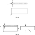
- the invention relates to a composite structure 9 for an acoustic wave device comprising a hetero-structure 5 (illustrated in FIG. figure 1c ).
- the latter includes a useful layer 2 of piezoelectric material, having a first 3 and a second face 4, as illustrated in FIG. It also includes a support substrate 1 having a coefficient of thermal expansion lower than that of the useful layer 2.
- the useful layer 2 is arranged along its first face 3 on the support substrate 1 ( figure 1b ).
- the useful layer 2 of the hetero-structure 5 may be composed of a material chosen from the group: lithium tantalate (LiTaO 3 ), lithium niobate (LiNbO 3 ), aluminum nitride (AlN), zinc oxide (ZnO).
- the support substrate 1 of the hetero-structure 5 may be composed of a material chosen from the group: silicon, III-V semiconductors, silicon carbide, glass, sapphire.
- the assembly of the useful layer 2 on the support substrate 1 is for example carried out by direct bonding by molecular adhesion.
- an additional layer (not shown), for example of silicon oxide, could be deposited on the support substrate 1 and / or on the first face 3 of the useful layer before assembly; this configuration could for example facilitate the bonding between the useful layer 2 and the support substrate 1.
- a hetero-structure 5 comprising a useful layer 2 made of piezoelectric material is of growing interest in the field of acoustic wave devices, in particular used for mobile phone applications and radio-frequency communications.
- the Applicant has noticed that good consolidation of the bonding interface between the useful layer 2 and the support substrate 1 promotes the strength of the hetero-structure 5 during the stages of development of the devices, in particular the treatment stages. thermal.
- the object of the composite structure 9 according to the invention is therefore in particular to allow the reinforcement of the bonding energy of the interface between the useful layer 2 and the support substrate 1 (called the first bonding interface) of the hetero-structure 5, with a view to subsequent stages in the development of devices.
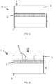
- the composite structure 9 according to the invention thus comprises a functional layer 6, having two faces 7 and 8 ( figure 1b ).
- This layer 6 is assembled on the second face 4 of the useful layer 2, so that the entire surface of one of its faces 7,8 (in this case face 7, on the figure 1c ) or disposed on the second face 4 of the useful layer 2 (at a second bonding interface).
- the functional layer 6 also has a thermal expansion coefficient lower than that of the useful layer 2.
- the functional layer 6 may be composed of a material chosen from the group: silicon, III-V semiconductors, silicon carbide, glass, sapphire.
- the functional layer 6 may be made of the same material as the support substrate 1.
- an intermediate layer (not shown) may be present between the functional layer 6 and the useful layer 2, for example made of silicon oxide, silicon nitride, etc.
- the intermediate layer may have been deposited on the second face 4 of the useful layer 2 and / or on the face 7 of the functional layer 6 before assembly.
- the composite structure 9 according to the invention is compatible with a heat treatment temperature greater than a limit temperature beyond which the hetero-structure 5 degrades or breaks in the absence of the functional layer 6.
- CTE coefficient of thermal expansion
- the hetero-structure 5 will deteriorate (cracking or breakage of the support substrate 1, detachment of the useful layer 2 at its level.
- first face 3, dislocation or deformation of the useful layer 2) if it is subjected to a temperature above a limit temperature; this limit temperature is linked to the difference in CTE between the useful layer 2 and the support substrate 1 and to the respective thicknesses of the useful layer 2 and of the support substrate 1.
- the limit temperature is of the order of 150 ° C.
- the composite structure 9 according to the invention allows the application of a temperature above this limit temperature.
- the addition of a functional layer 6 in Si with a thickness of 200 ⁇ m on the aforementioned example of hetero-structure 5 allows the application of a heat treatment in the range 200-400 ° C.
- a heat treatment in this temperature range is advantageous for the consolidation of the first bonding interface between the useful layer 2 and the support substrate 1 of the hetero-structure 5 and makes it possible to achieve bonding energies higher than one. treatment below 150 ° C.
- a hetero-structure 5 comprising a very thin useful layer 2 made of piezoelectric material can also be of interest in the field of acoustic wave devices, in particular BAW devices.
- One solution for manufacturing such a hetero-structure is to transfer said useful layer 2 by the Smart Cut® process, including the formation of a fragile plane buried in a piezoelectric material donor substrate by introduction of light species. such as hydrogen or helium, the direct bonding of this donor substrate on a support substrate 1 made of silicon, and the detachment at the level of the buried fragile plane so as to transfer a surface layer of piezoelectric material onto Si. that the surface layer after transfer still comprises defects and light species in its thickness, which can in particular degrade its piezoelectric characteristics.
- the suitable temperature range would be chosen between 400 ° and 600 ° C, ie below the temperature of Curie of the material.
- the object of the composite structure 9 according to the invention is also to allow the application of a healing annealing to the useful layer 2 of the hetero-structure 5, in order to restore its piezoelectric characteristics.
- the limit temperature is of the order of 400 ° C.
- the composite structure 9 according to the invention allows the application of a temperature above this limit temperature.
- the addition of a functional layer 6 in Si with a thickness of 50-100 ⁇ m on the aforementioned hetero-structure 5 allows the application of a heat treatment in the range 500-600 ° C.
- the functional layer 6 will have a thickness greater than or equal to 10 ⁇ m.
- the functional layer 6 will even have a thickness greater than or equal to 50 ⁇ m.
- the functional layer 6 is removed after the application, to the composite structure 9, of the heat treatment intended to consolidate the first bonding interface of the hetero-structure 5 and / or to cure all or part of the defects in the useful layer 2.
- the adhesion energy of the second bonding interface between the functional layer 6 and the second face 4 of the useful layer 2 of the hetero-structure 5 will be chosen less than 1000 mJ / m 2 , to allow the disassembly of the functional layer 6.
- the term disassembly is used here to translate the separation between the functional layer 6 and the hetero-structure 5 at the level of the second collage interface.
- the present invention thus makes it possible to obtain a hetero-structure 5 of which the mechanical strength (consolidated bonding interface) and the electrical characteristics (defects of the useful layer totally or partially cured) are compatible with the subsequent development of the devices to acoustic waves on the useful layer 2.
- the adhesion energy between the useful layer 2 and the support substrate 1 of the hetero-structure 5 is greater than or equal to 1500 mJ / m 2 .
- one or more first (s) local opening (s) 10 is (are) arranged in the functional layer 6 of the composite structure 9, allowing access to at least a first part 11 of the second face 4 of the useful layer 2. It is thus possible to produce components on the useful layer 2, at the level of the at least a first part 11.
- the first part 11 of the second face 4 of the useful layer comprises in particular metal elements 12 forming an acoustic wave device, in particular a SAW device ( figure 2b ).
- the metal elements 12 could for example consist of interdigitated electrodes and associated contact pads.
- the composite structure 9 according to this second variant can provide more advantageous mechanical strength than the hetero-structure 5 alone: it can in particular be compatible with higher heat treatments compared to a hetero-structure 9 without a functional layer 6, during manufacture of the acoustic wave device.
- the functional layer 6 comprises metal contacts 13 and / or electronic devices 14 electrically connected to certain metal elements 12 arranged on the useful layer 2.
- the composite structure 9 allows in this mode of implementation. work to deport the contact pads of the SAW devices present on the useful layer 2, on the face 8 of the functional layer 6; this configuration can be advantageous in particular to facilitate vertical interconnections and assembly with a cover 15 (“wafer level packaging”, illustrated on figure 2c ).
- the composite structure 9 also makes it possible to carry out a co-integration of components, some 12 produced on a piezoelectric material (the useful layer 2), others 14 produced on the functional layer 6 (for example a semiconductor layer of the silicon type). .
- the support substrate 1 itself also comprises one (or more) second local opening 16 allowing access to at least a second part 17 of the first face 3 of the useful layer 2.
- the second local opening 16 will be at least partially in vis-à-vis a first local opening 10 made in the functional layer 6; the first local opening 10 allows access to at least a first part 11 of the second face 4 of the useful layer 2.
- the first 11 and second 17 parts respectively of the second 4 and first 3 faces of the useful layer 2 comprise elements metal forming an acoustic wave device, for example a BAW device.
- the functional layer 6 and / or the support substrate 1 comprises (s) metal contacts 13,20 and / or electronic devices 14 electrically connected to certain metal elements 12,18 arranged on the first 11 and second 17 parts of the useful layer 2. As shown in the figure 3 , metal elements 18 arranged on the second part 17 of the useful layer 2 can be connected to contact pads 20 of the functional layer 6 using through conductive vias 19.
- the invention also relates to a method of manufacturing a composite structure 9 for an acoustic wave device.
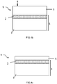
- the method includes a step of providing a hetero-structure 5 comprising a useful layer 2 of piezoelectric material, having a first face 3 and a second face 4 ( figure 4a ).
- the first face 3 is placed on a support substrate 1 having a thermal expansion coefficient lower than that of the useful layer 2.
- the method further comprises a step of assembling the entire surface of a face 7 of a functional layer. 6 ( figure 4a ) on the second face 4 of the useful layer 2 to form the composite structure 9 ( figure 4b ), the functional layer 6 having a thermal expansion coefficient lower than that of the useful layer 2.
- This assembly step may consist of direct bonding by molecular adhesion.
- the surfaces to be assembled respectively of the functional layer 6 and of the useful layer 2 may advantageously undergo a cleaning sequence making it possible to prepare them with a view to direct bonding.
- a chemical cleaning based on ozone then RCA could be applied as well as an O2 or N2 plasma treatment for surface activation.
- an intermediate layer could be deposited on the face 7 of the functional layer 6 and / or on the face 4 of the useful layer 2, for example a layer of silicon oxide or silicon nitride.
- the method according to the invention also comprises a step of heat treatment of the composite structure 9 at a temperature above a limit temperature above which the hetero-structure 5 degrades or breaks in the absence of the functional layer 6.
- CTE coefficient of thermal expansion
- the hetero-structure 5 will degrade (cracking or breakage of the support substrate 1, detachment of the useful layer 2 at its first face 3, dislocation or deformation of the useful layer 2) when a temperature above a limit temperature is applied to it; this limit temperature is linked to the difference in CTE between useful layer 2 and support substrate 1 and to the respective types and thicknesses of useful layer 2 and of support substrate 1.
- the composite structure 9 will thus be compatible with a temperature greater than or equal to 250 ° C, in particular between 250 ° and 600 ° C, depending on the materials and the respective thicknesses of the functional layers 6, useful 2 and of the support substrate 1.
- the method according to the invention comprises a step of making the functional layer 6 thicker ( figure 4c ), prior to the heat treatment step, to achieve a thickness of the functional layer 6 greater than or equal to a threshold thickness.
- this threshold thickness will be chosen to be greater than or equal to 10 ⁇ m.
- the functional layer 6 will even have a thickness greater than or equal to 50 ⁇ m.
- the thicknessing step can consist of mechanical, mechanical-chemical and / or chemical thinning.
- the method according to the invention can comprise a step of removing the functional layer 6 after the heat treatment step, by dismantling at a bonding interface of the composite structure 9. , between the functional layer 6 and the useful layer 2 (called the second bonding interface).
- the assembly step of the method between the functional layer 6 and the useful layer 2 will have been carried out so that the second bonding interface can be subsequently dismantled; in particular, it will have been carried out so that the bonding energy at this interface is less than 1000 mJ / m 2 .
- the assembly step may consist of an oxide / oxide bonding, the face 7 of the functional layer 6 and the face 4 of the useful layer 2 being provided with a layer of silicon oxide.
- the surface roughness of the oxide layers will be chosen in the range of 0.1 to 0.5 nm RMS, so as to obtain a bonding energy of less than 1000 mJ / m 2 , for example of the order of 500 mJ / m 2 .
- the dismantling, after the heat treatment step, could for example be carried out by applying a mechanical stress at the level of the second bonding interface of the composite structure 9, that is to say at the level of the interface. between the functional layer 9 and the useful layer 2.
- the hetero-structure 5 is obtained with a consolidated bonding interface, compatible with the subsequent steps in the manufacture of an acoustic wave device.
- the total removal of the functional layer 6 can be achieved using mechanical, mechanical-chemical or chemical thinning techniques.
- the method according to the invention comprises a step of local removal of the functional layer 6 to allow access to at least a first part 11 of the second face 4 of the useful layer 2.
- This local removal step can consist of wet or dry chemical etching in areas defined for example by photolithography techniques.
- a local shrinkage can be carried out on a plurality of zones allowing access to a percentage (opening rate) of the second face 4 of the useful layer 2; the opening rate may be between a few% and ⁇ 100%, depending on the devices to be developed.
- the method then comprises a step of producing acoustic wave devices comprising metallic elements 12 on the plurality of first parts 11 ( figure 2b ).
- This device production step may in particular include the production of contact pads 13 on the functional layer 6, electrically connected with the acoustic wave devices present on the useful layer 2.
- the method according to the invention may further comprise a step of local removal of the support substrate 1 to allow access to at least a second part 17 of the first face 3 of the useful layer 2.
- This local removal step can consist of wet or dry chemical etching in areas defined for example by photolithography techniques. By way of example, it is possible to carry out a local shrinkage on a plurality of zones with an opening rate of between 1 and 50%.
- the plurality of second parts 17 and the plurality of first parts 11 will be at least partially facing each other, thus making it possible to obtain a local self-contained membrane. useful layer range 2.
- the method then comprises a step of producing acoustic wave devices comprising elements metal 18 on the plurality of second parts 17 of the working layer 2, as illustrated in figure 3 .
- the method may include a step of making components 14 on the functional layer 6 and / or on the support substrate 1, and / or an electrical connection step between metal elements 12, 18 arranged on the useful layer 2 and contacts.
- metal 13, 20 arranged on the functional layer 6 and / or on the support substrate 1.
- a hetero-structure 5 comprising a useful layer 2 in lithium niobate (LiNbO3) with a thickness of 20 ⁇ m and a support substrate 1 in silicon (Si) with a thickness of 625 ⁇ m and 150 mm in diameter has an energy of bonding much lower than 1J / m 2 .
- LiNbO3 lithium niobate
- Si silicon
- the functional layer 6 is a silicon substrate (with a diameter of 150 mm and a thickness of 625 ⁇ m) comprising an intermediate layer of silicon oxide 400 nm thick on its front face 7.
- the silicon oxide layer has a roughness surface area of the order of 0.2 nm RMS.
- the functional layer 6 then undergoes cleaning (typically ozone and RCA), prior to its assembly on the second face 4 of the useful layer 2 of the hetero-structure 5.
- the heat treatment is then applied at 250 ° C for 2 hours at composite structure 9. This one is able to withstand a thermal budget of 250 ° C / 2h, without being damaged and without generating degradation of the hetero-structure 5.
- the hetero-structure 5, alone, would have undergone a degradation (cracking or breakage of the support substrate 1 and / or partial or total detachment of the useful layer 2), if it had been subjected before reinforcement of its bonding interface to this thermal budget, or even to a lower thermal budget of the around 200 ° C.
- the functional layer 6 is removed by inserting a bevel-shaped tool at the level of the bonding interface between the functional layer 6 and the useful layer 2.
- the heterostructure 5 has an interface of reinforced bonding, of the order of 1.5J / m 2, which gives it good mechanical strength during the subsequent stages in the production of acoustic wave devices.
- a hetero-structure 9 is formed from a useful layer 2 of lithium tantalate (LiTaO3) with a thickness of 0.3 ⁇ m and a support substrate 1 of silicon (Si) with a thickness of 625 ⁇ m and 150mm in diameter.
- the useful layer 2 was transferred by the Smart Cut® process and presents, after detachment, defects in its thickness which are prohibitive for the production of acoustic wave devices, because they impact the piezoelectric properties of the useful layer 2. Before the production of the wave devices acoustic on this hetero-structure 5, it is therefore essential to heal all or part of these defects; for this, it is necessary to apply a heat treatment to it at a temperature of 550 ° C, for 2 hours.
- the functional layer 6 is a silicon substrate (with a diameter of 150 mm and a thickness of 625 ⁇ m) comprising an intermediate layer of silicon oxide 400 nm thick on its front face 7; it undergoes a cleaning (typically ozone and RCA) and an O2 plasma treatment, prior to its assembly on the second face 4 of the useful layer 2 of the hetero-structure 5.
- a step of thickening the functional layer 6 is then operated by mechanical thinning (grinding), then by mechanical-chemical polishing, to a final thickness of 200 ⁇ m.
- the composite structure 9 thus formed is capable of withstanding a thermal budget of 550 ° C / 2h, without being damaged and without generating degradation of the hetero-structure 5.
- the hetero-structure 5, alone, would have undergone degradation ( cracking or breakage of the support substrate 1 and / or partial or total detachment of the useful layer 2), if it had been subjected to this thermal budget without the functional layer 6.
- the functional layer 6 is removed by adding a localized stress at the level of the second bonding interface between the functional layer 6 and the useful layer 2.
- the functional layer 6 is removed by a mechanical then chemical thinning sequence.
- the hetero-structure 5 has a reinforced bonding interface, greater than or equal to 1.5J / m 2 due to the thermal budget applied and the useful layer 2 has been cured of the majority of the defects linked to the implantation of species.
- light hydrogen or helium Smart Cut® process
- the level of healing of the defects in the useful layer 2 can be evaluated by making electrical devices and testing their level of performance, making it possible to validate the electrical quality of said useful layer 2.
- a hetero-structure 9 is formed from a useful layer 2 of lithium tantalate (LiTaO3) with a thickness of 0.3 ⁇ m and a support substrate 1 of silicon (Si) with a thickness of 625 ⁇ m and 150mm in diameter.
- the useful layer 2 was transferred by the Smart Cut® process and presents, after detachment, defects in its thickness which are prohibitive for the production of acoustic wave devices, because they impact the piezoelectric properties of the useful layer 2. Before the production of the wave devices acoustic on this hetero-structure 5, it is therefore essential to cure these defects; for this, it is necessary to apply a heat treatment to it at a temperature of 500 ° C, for 2 hours.
- the functional layer 6 is a silicon substrate (with a diameter of 150 mm and a thickness of 625 ⁇ m) comprising a intermediate layer of silicon oxide 400 nm thick on its front face 7; it undergoes a cleaning (typically ozone and RCA) and an O2 plasma treatment, prior to its assembly on the second face 4 of the useful layer 2 of the hetero-structure 9.
- a step of thickening the functional layer 6 is then operated by mechanical thinning (grinding), then by mechanical-chemical polishing, to a final thickness of 10 ⁇ m.
- the composite structure 9 thus formed is capable of withstanding a thermal budget of 500 ° C / 2h, without being damaged and without generating degradation of the hetero-structure 5.
- the hetero-structure 5, alone, would have undergone degradation ( cracking or breakage of the support substrate 1 and / or partial or total detachment of the useful layer 2), if it had been subjected to this thermal budget without the functional layer 6.
- the heterostructure 5 has a reinforced bonding interface, greater than 1.5J / m 2 due to the thermal budget applied and the useful layer 2 has been cured of a most of the defects linked to the implantation of light hydrogen or helium species (Smart Cut® process), becoming compatible with the production of acoustic wave devices.
- a local removal step of the functional layer 6 is then carried out to allow access to at least a first part 11 of the second face 4 of the useful layer 2.
- This local removal step can consist of wet or dry chemical etching. in areas defined by photolithography.
- the local withdrawal can be carried out on a plurality of zones allowing access to a plurality of first parts 11, and representing an opening rate of the order of 50%.
- Acoustic wave devices can then be produced on the plurality of first parts 11 of the useful layer 2. These devices comprise metallic elements 12, typically interdigitated electrodes.
- Contact pads 13 on the functional layer 6 can be electrically connected with the acoustic wave devices present on the useful layer 2.
- Components can also be produced on the functional layer 6.
- the composite structure 9 thus facilitates the co-integration of components produced on piezoelectric material (the useful layer) and on semiconductor material (the functional layer).
- the composite structure according to the invention is of great interest for the manufacture of acoustic wave devices, for example in the field of SAW and BAW filters for radio-frequency applications, but also in the field of piezoelectric sensors. Indeed, the latter allowing the transformation of mechanical movements into an electrical signal, and this with a very high sensitivity, several fields of application open up or are likely to open up in the fields of temperature sensors, energy. (“Energy harvesting”), etc.
Landscapes
- Physics & Mathematics (AREA)
- Acoustics & Sound (AREA)
- Engineering & Computer Science (AREA)
- Manufacturing & Machinery (AREA)
- Chemical & Material Sciences (AREA)
- Ceramic Engineering (AREA)
- Materials Engineering (AREA)
- Surface Acoustic Wave Elements And Circuit Networks Thereof (AREA)
- Piezo-Electric Or Mechanical Vibrators, Or Delay Or Filter Circuits (AREA)
Applications Claiming Priority (2)
| Application Number | Priority Date | Filing Date | Title |
|---|---|---|---|
| FR1559994A FR3042647B1 (fr) | 2015-10-20 | 2015-10-20 | Structure composite et procede de fabrication associe |
| PCT/FR2016/052675 WO2017068270A1 (fr) | 2015-10-20 | 2016-10-17 | Structure composite et procédé de fabrication associé |
Publications (2)
| Publication Number | Publication Date |
|---|---|
| EP3365927A1 EP3365927A1 (fr) | 2018-08-29 |
| EP3365927B1 true EP3365927B1 (fr) | 2021-03-24 |
Family
ID=54708030
Family Applications (1)
| Application Number | Title | Priority Date | Filing Date |
|---|---|---|---|
| EP16798236.2A Active EP3365927B1 (fr) | 2015-10-20 | 2016-10-17 | Structure composite et procédé de fabrication associé |
Country Status (8)
| Country | Link |
|---|---|
| US (1) | US20180316329A1 (enExample) |
| EP (1) | EP3365927B1 (enExample) |
| JP (1) | JP6923518B2 (enExample) |
| KR (1) | KR102671257B1 (enExample) |
| CN (2) | CN108271425A (enExample) |
| FR (1) | FR3042647B1 (enExample) |
| SG (1) | SG11201803341QA (enExample) |
| WO (1) | WO2017068270A1 (enExample) |
Families Citing this family (12)
| Publication number | Priority date | Publication date | Assignee | Title |
|---|---|---|---|---|
| FR3068508B1 (fr) * | 2017-06-30 | 2019-07-26 | Soitec | Procede de transfert d'une couche mince sur un substrat support presentant des coefficients de dilatation thermique differents |
| FR3076126A1 (fr) * | 2017-12-26 | 2019-06-28 | Commissariat A L'energie Atomique Et Aux Energies Alternatives | Procede de realisation d'un resonateur acoustique a ondes de volume a capacite parasite reduite |
| FR3079346B1 (fr) * | 2018-03-26 | 2020-05-29 | Soitec | Procede de fabrication d'un substrat donneur pour le transfert d'une couche piezoelectrique, et procede de transfert d'une telle couche piezoelectrique |
| WO2020198934A1 (en) | 2019-03-29 | 2020-10-08 | Shenzhen Xpectvision Technology Co., Ltd. | Semiconductor x-ray detector |
| US11750172B2 (en) | 2019-08-21 | 2023-09-05 | Skyworks Solutions, Inc. | Multilayer piezoelectric substrate |
| US11722122B2 (en) | 2019-11-22 | 2023-08-08 | Skyworks Solutions, Inc. | Multilayer piezoelectric substrate with high density electrode |
| CN111883644B (zh) * | 2020-07-23 | 2021-04-13 | 中国科学院上海微系统与信息技术研究所 | 一种异质压电薄膜结构及其制备方法 |
| GB2598665B (en) * | 2020-09-04 | 2025-07-23 | Skyworks Solutions Inc | Multi-layer piezoelectric substrate with controllable delta temperature coefficient of frequency |
| EP3989299B1 (en) * | 2020-10-26 | 2025-08-06 | Université de Franche-Comté | Piezoelectric device comprising flexible single crystalline piezoelectric linbo3 and/or litao3 films integrated on flexible substrate and methods for producing the same |
| US12483226B2 (en) | 2021-12-29 | 2025-11-25 | Skyworks Solutions, Inc. | Acoustic wave device with tilted multilayer interdigital transducer electrode |
| US20230223910A1 (en) | 2022-01-13 | 2023-07-13 | Skyworks Solutions, Inc. | Method of making acoustic wave device with vertically mass loaded multi-layer interdigital transducer electrode for transverse mode suppression |
| US12500572B2 (en) | 2022-04-15 | 2025-12-16 | Skyworks Solutions, Inc. | Multiplexer formed on multi-layer piezoelectric substrate and temperature compensated surface acoustic wave device dies |
Family Cites Families (20)
| Publication number | Priority date | Publication date | Assignee | Title |
|---|---|---|---|---|
| TW219354B (en) * | 1993-05-31 | 1994-01-21 | Ind Tech Res Inst | Strengthening of multi-layer ceramic/glass articles |
| JPH10297931A (ja) * | 1997-04-24 | 1998-11-10 | Matsushita Electric Ind Co Ltd | 複合圧電基板の製造方法 |
| TW449937B (en) * | 1999-02-26 | 2001-08-11 | Matsushita Electronics Corp | Semiconductor device and the manufacturing method thereof |
| FR2816445B1 (fr) * | 2000-11-06 | 2003-07-25 | Commissariat Energie Atomique | Procede de fabrication d'une structure empilee comprenant une couche mince adherant a un substrat cible |
| JP3815424B2 (ja) * | 2002-11-08 | 2006-08-30 | 株式会社村田製作所 | 弾性境界波装置 |
| FR2856192B1 (fr) * | 2003-06-11 | 2005-07-29 | Soitec Silicon On Insulator | Procede de realisation de structure heterogene et structure obtenue par un tel procede |
| WO2005069486A1 (ja) * | 2004-01-19 | 2005-07-28 | Murata Manufacturing Co., Ltd. | 弾性境界波装置 |
| WO2007142112A1 (ja) * | 2006-06-02 | 2007-12-13 | Murata Manufacturing Co., Ltd. | 多層セラミック基板およびその製造方法ならびに電子部品 |
| US7608986B2 (en) * | 2006-10-02 | 2009-10-27 | Seiko Epson Corporation | Quartz crystal resonator |
| JP4894861B2 (ja) * | 2006-12-25 | 2012-03-14 | 株式会社村田製作所 | 弾性境界波装置 |
| US7408286B1 (en) * | 2007-01-17 | 2008-08-05 | Rf Micro Devices, Inc. | Piezoelectric substrate for a saw device |
| JP5104761B2 (ja) * | 2007-04-09 | 2012-12-19 | 株式会社村田製作所 | セラミック基板およびその製造方法 |
| JP2009124696A (ja) * | 2007-10-26 | 2009-06-04 | Panasonic Electric Works Co Ltd | 共振装置 |
| CN101874429B (zh) * | 2007-11-30 | 2013-04-03 | 株式会社村田制作所 | 陶瓷复合多层基板及其制造方法以及电子元器件 |
| JP4460612B2 (ja) * | 2008-02-08 | 2010-05-12 | 富士通メディアデバイス株式会社 | 弾性表面波デバイス及びその製造方法 |
| CN104589738A (zh) * | 2008-05-15 | 2015-05-06 | 株式会社村田制作所 | 多层陶瓷基板及其制造方法 |
| FR2942911B1 (fr) * | 2009-03-09 | 2011-05-13 | Soitec Silicon On Insulator | Procede de realisation d'une heterostructure avec adaptation locale de coefficient de dilatation thermique |
| WO2014129432A1 (ja) * | 2013-02-19 | 2014-08-28 | 日本碍子株式会社 | 複合基板、弾性波デバイス及び弾性波デバイスの製法 |
| JP6242597B2 (ja) * | 2013-06-03 | 2017-12-06 | 太陽誘電株式会社 | 弾性波デバイス及びその製造方法 |
| US9646911B2 (en) * | 2014-04-10 | 2017-05-09 | Sensor Electronic Technology, Inc. | Composite substrate |
-
2015
- 2015-10-20 FR FR1559994A patent/FR3042647B1/fr active Active
-
2016
- 2016-10-17 EP EP16798236.2A patent/EP3365927B1/fr active Active
- 2016-10-17 SG SG11201803341QA patent/SG11201803341QA/en unknown
- 2016-10-17 KR KR1020187014265A patent/KR102671257B1/ko active Active
- 2016-10-17 WO PCT/FR2016/052675 patent/WO2017068270A1/fr not_active Ceased
- 2016-10-17 US US15/769,698 patent/US20180316329A1/en active Pending
- 2016-10-17 CN CN201680065643.1A patent/CN108271425A/zh active Pending
- 2016-10-17 JP JP2018520170A patent/JP6923518B2/ja active Active
- 2016-10-17 CN CN202210146142.3A patent/CN114512595A/zh active Pending
Non-Patent Citations (1)
| Title |
|---|
| None * |
Also Published As
| Publication number | Publication date |
|---|---|
| WO2017068270A1 (fr) | 2017-04-27 |
| CN108271425A (zh) | 2018-07-10 |
| JP2018537888A (ja) | 2018-12-20 |
| US20180316329A1 (en) | 2018-11-01 |
| CN114512595A (zh) | 2022-05-17 |
| EP3365927A1 (fr) | 2018-08-29 |
| FR3042647B1 (fr) | 2017-12-01 |
| SG11201803341QA (en) | 2018-05-30 |
| KR102671257B1 (ko) | 2024-06-03 |
| JP6923518B2 (ja) | 2021-08-18 |
| KR20180074732A (ko) | 2018-07-03 |
| FR3042647A1 (fr) | 2017-04-21 |
Similar Documents
| Publication | Publication Date | Title |
|---|---|---|
| EP3365927B1 (fr) | Structure composite et procédé de fabrication associé | |
| EP3859800B1 (fr) | Structure hybride pour dispositif a ondes acoustiques de surface | |
| FR3068508B1 (fr) | Procede de transfert d'une couche mince sur un substrat support presentant des coefficients de dilatation thermique differents | |
| EP2591515B1 (fr) | Procede d'implantation d'un materiau piezoelectrique | |
| FR3042648A1 (fr) | Dispositif a ondes acoustiques de surface et procede de fabrication associe | |
| EP3394908B1 (fr) | Substrat pour un dispositif a ondes acoustiques de surface ou a ondes acoustiques de volume compense en temperature | |
| EP3465784B1 (fr) | Structure hybride pour dispositif a ondes acoustiques de surface | |
| FR3116652A1 (fr) | Procédé de fabrication d’un composant comprenant une couche en matériau monocristallin compatible avec des budgets thermiques élevés | |
| KR102882561B1 (ko) | 복합 기판의 제조 방법 및 복합 기판 | |
| EP3365929B1 (fr) | Procédé de fabrication d'une structure hybride | |
| EP4128380B1 (fr) | Procede de fabrication d'une structure piezoelectrique pour dispositif radiofrequence et servant pour le transfert d'une couche piezoelectrique, et procede de transfert d'une telle couche piezoelectrique | |
| TWI867180B (zh) | 用於製作射頻裝置用壓電結構之方法,該壓電結構可用於壓電層的移轉,以及移轉該壓電層之方法 |
Legal Events
| Date | Code | Title | Description |
|---|---|---|---|
| STAA | Information on the status of an ep patent application or granted ep patent |
Free format text: STATUS: UNKNOWN |
|
| STAA | Information on the status of an ep patent application or granted ep patent |
Free format text: STATUS: THE INTERNATIONAL PUBLICATION HAS BEEN MADE |
|
| PUAI | Public reference made under article 153(3) epc to a published international application that has entered the european phase |
Free format text: ORIGINAL CODE: 0009012 |
|
| STAA | Information on the status of an ep patent application or granted ep patent |
Free format text: STATUS: REQUEST FOR EXAMINATION WAS MADE |
|
| 17P | Request for examination filed |
Effective date: 20180410 |
|
| AK | Designated contracting states |
Kind code of ref document: A1 Designated state(s): AL AT BE BG CH CY CZ DE DK EE ES FI FR GB GR HR HU IE IS IT LI LT LU LV MC MK MT NL NO PL PT RO RS SE SI SK SM TR |
|
| AX | Request for extension of the european patent |
Extension state: BA ME |
|
| DAV | Request for validation of the european patent (deleted) | ||
| DAX | Request for extension of the european patent (deleted) | ||
| GRAP | Despatch of communication of intention to grant a patent |
Free format text: ORIGINAL CODE: EPIDOSNIGR1 |
|
| STAA | Information on the status of an ep patent application or granted ep patent |
Free format text: STATUS: GRANT OF PATENT IS INTENDED |
|
| GRAS | Grant fee paid |
Free format text: ORIGINAL CODE: EPIDOSNIGR3 |
|
| INTG | Intention to grant announced |
Effective date: 20210119 |
|
| GRAA | (expected) grant |
Free format text: ORIGINAL CODE: 0009210 |
|
| STAA | Information on the status of an ep patent application or granted ep patent |
Free format text: STATUS: THE PATENT HAS BEEN GRANTED |
|
| AK | Designated contracting states |
Kind code of ref document: B1 Designated state(s): AL AT BE BG CH CY CZ DE DK EE ES FI FR GB GR HR HU IE IS IT LI LT LU LV MC MK MT NL NO PL PT RO RS SE SI SK SM TR |
|
| REG | Reference to a national code |
Ref country code: GB Ref legal event code: FG4D Free format text: NOT ENGLISH |
|
| REG | Reference to a national code |
Ref country code: CH Ref legal event code: EP |
|
| REG | Reference to a national code |
Ref country code: IE Ref legal event code: FG4D Free format text: LANGUAGE OF EP DOCUMENT: FRENCH |
|
| REG | Reference to a national code |
Ref country code: AT Ref legal event code: REF Ref document number: 1375400 Country of ref document: AT Kind code of ref document: T Effective date: 20210415 Ref country code: DE Ref legal event code: R096 Ref document number: 602016054907 Country of ref document: DE Ref country code: CH Ref legal event code: NV Representative=s name: NOVAGRAAF INTERNATIONAL SA, CH |
|
| REG | Reference to a national code |
Ref country code: FI Ref legal event code: FGE |
|
| REG | Reference to a national code |
Ref country code: LT Ref legal event code: MG9D |
|
| PG25 | Lapsed in a contracting state [announced via postgrant information from national office to epo] |
Ref country code: NO Free format text: LAPSE BECAUSE OF FAILURE TO SUBMIT A TRANSLATION OF THE DESCRIPTION OR TO PAY THE FEE WITHIN THE PRESCRIBED TIME-LIMIT Effective date: 20210624 Ref country code: GR Free format text: LAPSE BECAUSE OF FAILURE TO SUBMIT A TRANSLATION OF THE DESCRIPTION OR TO PAY THE FEE WITHIN THE PRESCRIBED TIME-LIMIT Effective date: 20210625 Ref country code: HR Free format text: LAPSE BECAUSE OF FAILURE TO SUBMIT A TRANSLATION OF THE DESCRIPTION OR TO PAY THE FEE WITHIN THE PRESCRIBED TIME-LIMIT Effective date: 20210324 Ref country code: BG Free format text: LAPSE BECAUSE OF FAILURE TO SUBMIT A TRANSLATION OF THE DESCRIPTION OR TO PAY THE FEE WITHIN THE PRESCRIBED TIME-LIMIT Effective date: 20210624 |
|
| PG25 | Lapsed in a contracting state [announced via postgrant information from national office to epo] |
Ref country code: SE Free format text: LAPSE BECAUSE OF FAILURE TO SUBMIT A TRANSLATION OF THE DESCRIPTION OR TO PAY THE FEE WITHIN THE PRESCRIBED TIME-LIMIT Effective date: 20210324 Ref country code: LV Free format text: LAPSE BECAUSE OF FAILURE TO SUBMIT A TRANSLATION OF THE DESCRIPTION OR TO PAY THE FEE WITHIN THE PRESCRIBED TIME-LIMIT Effective date: 20210324 Ref country code: RS Free format text: LAPSE BECAUSE OF FAILURE TO SUBMIT A TRANSLATION OF THE DESCRIPTION OR TO PAY THE FEE WITHIN THE PRESCRIBED TIME-LIMIT Effective date: 20210324 |
|
| REG | Reference to a national code |
Ref country code: NL Ref legal event code: MP Effective date: 20210324 |
|
| REG | Reference to a national code |
Ref country code: AT Ref legal event code: MK05 Ref document number: 1375400 Country of ref document: AT Kind code of ref document: T Effective date: 20210324 |
|
| PG25 | Lapsed in a contracting state [announced via postgrant information from national office to epo] |
Ref country code: NL Free format text: LAPSE BECAUSE OF FAILURE TO SUBMIT A TRANSLATION OF THE DESCRIPTION OR TO PAY THE FEE WITHIN THE PRESCRIBED TIME-LIMIT Effective date: 20210324 |
|
| PG25 | Lapsed in a contracting state [announced via postgrant information from national office to epo] |
Ref country code: SM Free format text: LAPSE BECAUSE OF FAILURE TO SUBMIT A TRANSLATION OF THE DESCRIPTION OR TO PAY THE FEE WITHIN THE PRESCRIBED TIME-LIMIT Effective date: 20210324 Ref country code: AT Free format text: LAPSE BECAUSE OF FAILURE TO SUBMIT A TRANSLATION OF THE DESCRIPTION OR TO PAY THE FEE WITHIN THE PRESCRIBED TIME-LIMIT Effective date: 20210324 Ref country code: CZ Free format text: LAPSE BECAUSE OF FAILURE TO SUBMIT A TRANSLATION OF THE DESCRIPTION OR TO PAY THE FEE WITHIN THE PRESCRIBED TIME-LIMIT Effective date: 20210324 Ref country code: EE Free format text: LAPSE BECAUSE OF FAILURE TO SUBMIT A TRANSLATION OF THE DESCRIPTION OR TO PAY THE FEE WITHIN THE PRESCRIBED TIME-LIMIT Effective date: 20210324 Ref country code: LT Free format text: LAPSE BECAUSE OF FAILURE TO SUBMIT A TRANSLATION OF THE DESCRIPTION OR TO PAY THE FEE WITHIN THE PRESCRIBED TIME-LIMIT Effective date: 20210324 |
|
| PG25 | Lapsed in a contracting state [announced via postgrant information from national office to epo] |
Ref country code: SK Free format text: LAPSE BECAUSE OF FAILURE TO SUBMIT A TRANSLATION OF THE DESCRIPTION OR TO PAY THE FEE WITHIN THE PRESCRIBED TIME-LIMIT Effective date: 20210324 Ref country code: PT Free format text: LAPSE BECAUSE OF FAILURE TO SUBMIT A TRANSLATION OF THE DESCRIPTION OR TO PAY THE FEE WITHIN THE PRESCRIBED TIME-LIMIT Effective date: 20210726 Ref country code: PL Free format text: LAPSE BECAUSE OF FAILURE TO SUBMIT A TRANSLATION OF THE DESCRIPTION OR TO PAY THE FEE WITHIN THE PRESCRIBED TIME-LIMIT Effective date: 20210324 Ref country code: RO Free format text: LAPSE BECAUSE OF FAILURE TO SUBMIT A TRANSLATION OF THE DESCRIPTION OR TO PAY THE FEE WITHIN THE PRESCRIBED TIME-LIMIT Effective date: 20210324 Ref country code: IS Free format text: LAPSE BECAUSE OF FAILURE TO SUBMIT A TRANSLATION OF THE DESCRIPTION OR TO PAY THE FEE WITHIN THE PRESCRIBED TIME-LIMIT Effective date: 20210724 |
|
| REG | Reference to a national code |
Ref country code: DE Ref legal event code: R097 Ref document number: 602016054907 Country of ref document: DE |
|
| PG25 | Lapsed in a contracting state [announced via postgrant information from national office to epo] |
Ref country code: DK Free format text: LAPSE BECAUSE OF FAILURE TO SUBMIT A TRANSLATION OF THE DESCRIPTION OR TO PAY THE FEE WITHIN THE PRESCRIBED TIME-LIMIT Effective date: 20210324 Ref country code: ES Free format text: LAPSE BECAUSE OF FAILURE TO SUBMIT A TRANSLATION OF THE DESCRIPTION OR TO PAY THE FEE WITHIN THE PRESCRIBED TIME-LIMIT Effective date: 20210324 Ref country code: AL Free format text: LAPSE BECAUSE OF FAILURE TO SUBMIT A TRANSLATION OF THE DESCRIPTION OR TO PAY THE FEE WITHIN THE PRESCRIBED TIME-LIMIT Effective date: 20210324 |
|
| PLBE | No opposition filed within time limit |
Free format text: ORIGINAL CODE: 0009261 |
|
| STAA | Information on the status of an ep patent application or granted ep patent |
Free format text: STATUS: NO OPPOSITION FILED WITHIN TIME LIMIT |
|
| PG25 | Lapsed in a contracting state [announced via postgrant information from national office to epo] |
Ref country code: SI Free format text: LAPSE BECAUSE OF FAILURE TO SUBMIT A TRANSLATION OF THE DESCRIPTION OR TO PAY THE FEE WITHIN THE PRESCRIBED TIME-LIMIT Effective date: 20210324 |
|
| 26N | No opposition filed |
Effective date: 20220104 |
|
| PG25 | Lapsed in a contracting state [announced via postgrant information from national office to epo] |
Ref country code: IS Free format text: LAPSE BECAUSE OF FAILURE TO SUBMIT A TRANSLATION OF THE DESCRIPTION OR TO PAY THE FEE WITHIN THE PRESCRIBED TIME-LIMIT Effective date: 20210724 |
|
| PG25 | Lapsed in a contracting state [announced via postgrant information from national office to epo] |
Ref country code: MC Free format text: LAPSE BECAUSE OF FAILURE TO SUBMIT A TRANSLATION OF THE DESCRIPTION OR TO PAY THE FEE WITHIN THE PRESCRIBED TIME-LIMIT Effective date: 20210324 |
|
| PG25 | Lapsed in a contracting state [announced via postgrant information from national office to epo] |
Ref country code: LU Free format text: LAPSE BECAUSE OF NON-PAYMENT OF DUE FEES Effective date: 20211017 |
|
| PG25 | Lapsed in a contracting state [announced via postgrant information from national office to epo] |
Ref country code: IE Free format text: LAPSE BECAUSE OF NON-PAYMENT OF DUE FEES Effective date: 20211017 |
|
| REG | Reference to a national code |
Ref country code: DE Ref legal event code: R079 Ref document number: 602016054907 Country of ref document: DE Free format text: PREVIOUS MAIN CLASS: H01L0041080000 Ipc: H10N0030000000 |
|
| PG25 | Lapsed in a contracting state [announced via postgrant information from national office to epo] |
Ref country code: HU Free format text: LAPSE BECAUSE OF FAILURE TO SUBMIT A TRANSLATION OF THE DESCRIPTION OR TO PAY THE FEE WITHIN THE PRESCRIBED TIME-LIMIT; INVALID AB INITIO Effective date: 20161017 |
|
| PG25 | Lapsed in a contracting state [announced via postgrant information from national office to epo] |
Ref country code: CY Free format text: LAPSE BECAUSE OF FAILURE TO SUBMIT A TRANSLATION OF THE DESCRIPTION OR TO PAY THE FEE WITHIN THE PRESCRIBED TIME-LIMIT Effective date: 20210324 |
|
| PG25 | Lapsed in a contracting state [announced via postgrant information from national office to epo] |
Ref country code: MK Free format text: LAPSE BECAUSE OF FAILURE TO SUBMIT A TRANSLATION OF THE DESCRIPTION OR TO PAY THE FEE WITHIN THE PRESCRIBED TIME-LIMIT Effective date: 20210324 |
|
| PG25 | Lapsed in a contracting state [announced via postgrant information from national office to epo] |
Ref country code: TR Free format text: LAPSE BECAUSE OF FAILURE TO SUBMIT A TRANSLATION OF THE DESCRIPTION OR TO PAY THE FEE WITHIN THE PRESCRIBED TIME-LIMIT Effective date: 20210324 |
|
| PG25 | Lapsed in a contracting state [announced via postgrant information from national office to epo] |
Ref country code: MT Free format text: LAPSE BECAUSE OF FAILURE TO SUBMIT A TRANSLATION OF THE DESCRIPTION OR TO PAY THE FEE WITHIN THE PRESCRIBED TIME-LIMIT Effective date: 20210324 |
|
| PGFP | Annual fee paid to national office [announced via postgrant information from national office to epo] |
Ref country code: DE Payment date: 20240904 Year of fee payment: 9 |
|
| PGFP | Annual fee paid to national office [announced via postgrant information from national office to epo] |
Ref country code: FI Payment date: 20241015 Year of fee payment: 9 |
|
| PGFP | Annual fee paid to national office [announced via postgrant information from national office to epo] |
Ref country code: CH Payment date: 20241101 Year of fee payment: 9 |
|
| PGFP | Annual fee paid to national office [announced via postgrant information from national office to epo] |
Ref country code: IT Payment date: 20250922 Year of fee payment: 10 |
|
| PGFP | Annual fee paid to national office [announced via postgrant information from national office to epo] |
Ref country code: BE Payment date: 20250917 Year of fee payment: 10 Ref country code: GB Payment date: 20250904 Year of fee payment: 10 |
|
| PGFP | Annual fee paid to national office [announced via postgrant information from national office to epo] |
Ref country code: FR Payment date: 20250922 Year of fee payment: 10 |
|
| REG | Reference to a national code |
Ref country code: CH Ref legal event code: U11 Free format text: ST27 STATUS EVENT CODE: U-0-0-U10-U11 (AS PROVIDED BY THE NATIONAL OFFICE) Effective date: 20251101 |