EP3361495A1 - Matériau hybride en polymère, son procédé de fabrication ainsi que son utilisation et procédé de fractionnement - Google Patents
Matériau hybride en polymère, son procédé de fabrication ainsi que son utilisation et procédé de fractionnement Download PDFInfo
- Publication number
- EP3361495A1 EP3361495A1 EP18163583.0A EP18163583A EP3361495A1 EP 3361495 A1 EP3361495 A1 EP 3361495A1 EP 18163583 A EP18163583 A EP 18163583A EP 3361495 A1 EP3361495 A1 EP 3361495A1
- Authority
- EP
- European Patent Office
- Prior art keywords
- polymer
- fillers
- hybrid material
- solid
- matrix
- Prior art date
- Legal status (The legal status is an assumption and is not a legal conclusion. Google has not performed a legal analysis and makes no representation as to the accuracy of the status listed.)
- Pending
Links
- 239000000463 material Substances 0.000 title claims abstract description 112
- 238000000034 method Methods 0.000 title claims abstract description 73
- 238000004519 manufacturing process Methods 0.000 title claims abstract description 16
- 229920000642 polymer Polymers 0.000 claims abstract description 146
- 239000007787 solid Substances 0.000 claims abstract description 145
- 239000000945 filler Substances 0.000 claims abstract description 85
- 239000011159 matrix material Substances 0.000 claims abstract description 56
- 239000007858 starting material Substances 0.000 claims abstract description 42
- 230000008569 process Effects 0.000 claims abstract description 32
- 229910052751 metal Inorganic materials 0.000 claims abstract description 15
- 239000002184 metal Substances 0.000 claims abstract description 15
- 239000002131 composite material Substances 0.000 claims abstract description 7
- 229920001971 elastomer Polymers 0.000 claims abstract description 7
- 239000000806 elastomer Substances 0.000 claims abstract description 7
- 239000002245 particle Substances 0.000 claims description 25
- VYPSYNLAJGMNEJ-UHFFFAOYSA-N Silicium dioxide Chemical compound O=[Si]=O VYPSYNLAJGMNEJ-UHFFFAOYSA-N 0.000 claims description 13
- XEEYBQQBJWHFJM-UHFFFAOYSA-N Iron Chemical compound [Fe] XEEYBQQBJWHFJM-UHFFFAOYSA-N 0.000 claims description 10
- 238000006243 chemical reaction Methods 0.000 claims description 9
- 239000004205 dimethyl polysiloxane Substances 0.000 claims description 9
- 229920000435 poly(dimethylsiloxane) Polymers 0.000 claims description 9
- 229910052782 aluminium Inorganic materials 0.000 claims description 8
- XAGFODPZIPBFFR-UHFFFAOYSA-N aluminium Chemical compound [Al] XAGFODPZIPBFFR-UHFFFAOYSA-N 0.000 claims description 8
- 239000011258 core-shell material Substances 0.000 claims description 8
- -1 polydimethylsiloxane Polymers 0.000 claims description 8
- 239000000376 reactant Substances 0.000 claims description 8
- 239000011701 zinc Substances 0.000 claims description 8
- HCHKCACWOHOZIP-UHFFFAOYSA-N Zinc Chemical compound [Zn] HCHKCACWOHOZIP-UHFFFAOYSA-N 0.000 claims description 7
- 229910052725 zinc Inorganic materials 0.000 claims description 7
- RYGMFSIKBFXOCR-UHFFFAOYSA-N Copper Chemical compound [Cu] RYGMFSIKBFXOCR-UHFFFAOYSA-N 0.000 claims description 6
- 229910052802 copper Inorganic materials 0.000 claims description 6
- 239000010949 copper Substances 0.000 claims description 6
- 229920002748 Basalt fiber Polymers 0.000 claims description 5
- OKTJSMMVPCPJKN-UHFFFAOYSA-N Carbon Chemical compound [C] OKTJSMMVPCPJKN-UHFFFAOYSA-N 0.000 claims description 5
- 229910052799 carbon Inorganic materials 0.000 claims description 5
- 239000011521 glass Substances 0.000 claims description 5
- 239000012784 inorganic fiber Substances 0.000 claims description 5
- 229910052742 iron Inorganic materials 0.000 claims description 5
- 239000007800 oxidant agent Substances 0.000 claims description 5
- 238000002360 preparation method Methods 0.000 claims description 5
- 239000000377 silicon dioxide Substances 0.000 claims description 5
- 230000006872 improvement Effects 0.000 claims description 4
- 239000003054 catalyst Substances 0.000 claims description 2
- 239000003112 inhibitor Substances 0.000 claims description 2
- 239000003999 initiator Substances 0.000 claims description 2
- YPFNIPKMNMDDDB-UHFFFAOYSA-K 2-[2-[bis(carboxylatomethyl)amino]ethyl-(2-hydroxyethyl)amino]acetate;iron(3+) Chemical compound [Fe+3].OCCN(CC([O-])=O)CCN(CC([O-])=O)CC([O-])=O YPFNIPKMNMDDDB-UHFFFAOYSA-K 0.000 claims 1
- 239000003795 chemical substances by application Substances 0.000 claims 1
- 235000012431 wafers Nutrition 0.000 description 38
- 230000007547 defect Effects 0.000 description 22
- 230000005855 radiation Effects 0.000 description 19
- 239000000919 ceramic Substances 0.000 description 11
- 238000009826 distribution Methods 0.000 description 10
- 239000004065 semiconductor Substances 0.000 description 10
- 229910052594 sapphire Inorganic materials 0.000 description 9
- 239000010980 sapphire Substances 0.000 description 9
- 238000001816 cooling Methods 0.000 description 8
- 238000004062 sedimentation Methods 0.000 description 8
- VEXZGXHMUGYJMC-UHFFFAOYSA-N Hydrochloric acid Chemical compound Cl VEXZGXHMUGYJMC-UHFFFAOYSA-N 0.000 description 7
- XUIMIQQOPSSXEZ-UHFFFAOYSA-N Silicon Chemical compound [Si] XUIMIQQOPSSXEZ-UHFFFAOYSA-N 0.000 description 7
- 238000004132 cross linking Methods 0.000 description 7
- 238000000354 decomposition reaction Methods 0.000 description 7
- 229910052710 silicon Inorganic materials 0.000 description 7
- 239000010703 silicon Substances 0.000 description 7
- JBRZTFJDHDCESZ-UHFFFAOYSA-N AsGa Chemical compound [As]#[Ga] JBRZTFJDHDCESZ-UHFFFAOYSA-N 0.000 description 6
- 229910001218 Gallium arsenide Inorganic materials 0.000 description 6
- HBMJWWWQQXIZIP-UHFFFAOYSA-N silicon carbide Chemical compound [Si+]#[C-] HBMJWWWQQXIZIP-UHFFFAOYSA-N 0.000 description 6
- 229910010271 silicon carbide Inorganic materials 0.000 description 6
- 239000000758 substrate Substances 0.000 description 6
- 230000008901 benefit Effects 0.000 description 5
- 230000006378 damage Effects 0.000 description 5
- 230000000737 periodic effect Effects 0.000 description 5
- 229920006254 polymer film Polymers 0.000 description 5
- 239000002904 solvent Substances 0.000 description 5
- IJGRMHOSHXDMSA-UHFFFAOYSA-N Atomic nitrogen Chemical compound N#N IJGRMHOSHXDMSA-UHFFFAOYSA-N 0.000 description 4
- 229910002601 GaN Inorganic materials 0.000 description 4
- GPXJNWSHGFTCBW-UHFFFAOYSA-N Indium phosphide Chemical compound [In]#P GPXJNWSHGFTCBW-UHFFFAOYSA-N 0.000 description 4
- 241000960387 Torque teno virus Species 0.000 description 4
- XLOMVQKBTHCTTD-UHFFFAOYSA-N Zinc monoxide Chemical compound [Zn]=O XLOMVQKBTHCTTD-UHFFFAOYSA-N 0.000 description 4
- PNEYBMLMFCGWSK-UHFFFAOYSA-N aluminium oxide Inorganic materials [O-2].[O-2].[O-2].[Al+3].[Al+3] PNEYBMLMFCGWSK-UHFFFAOYSA-N 0.000 description 4
- JNDMLEXHDPKVFC-UHFFFAOYSA-N aluminum;oxygen(2-);yttrium(3+) Chemical compound [O-2].[O-2].[O-2].[Al+3].[Y+3] JNDMLEXHDPKVFC-UHFFFAOYSA-N 0.000 description 4
- 229910010293 ceramic material Inorganic materials 0.000 description 4
- 239000007795 chemical reaction product Substances 0.000 description 4
- 230000001419 dependent effect Effects 0.000 description 4
- 238000004090 dissolution Methods 0.000 description 4
- 239000012530 fluid Substances 0.000 description 4
- 230000009477 glass transition Effects 0.000 description 4
- 230000000087 stabilizing effect Effects 0.000 description 4
- 238000010897 surface acoustic wave method Methods 0.000 description 4
- 239000012780 transparent material Substances 0.000 description 4
- 229910019901 yttrium aluminum garnet Inorganic materials 0.000 description 4
- 230000008859 change Effects 0.000 description 3
- KRKNYBCHXYNGOX-UHFFFAOYSA-N citric acid Chemical compound OC(=O)CC(O)(C(O)=O)CC(O)=O KRKNYBCHXYNGOX-UHFFFAOYSA-N 0.000 description 3
- 239000000835 fiber Substances 0.000 description 3
- 229910052732 germanium Inorganic materials 0.000 description 3
- GNPVGFCGXDBREM-UHFFFAOYSA-N germanium atom Chemical compound [Ge] GNPVGFCGXDBREM-UHFFFAOYSA-N 0.000 description 3
- 230000000977 initiatory effect Effects 0.000 description 3
- 230000003993 interaction Effects 0.000 description 3
- 239000000203 mixture Substances 0.000 description 3
- 229910003465 moissanite Inorganic materials 0.000 description 3
- 238000012546 transfer Methods 0.000 description 3
- 229910018072 Al 2 O 3 Inorganic materials 0.000 description 2
- 229910005540 GaP Inorganic materials 0.000 description 2
- 229910000673 Indium arsenide Inorganic materials 0.000 description 2
- WHXSMMKQMYFTQS-UHFFFAOYSA-N Lithium Chemical compound [Li] WHXSMMKQMYFTQS-UHFFFAOYSA-N 0.000 description 2
- 229910000577 Silicon-germanium Inorganic materials 0.000 description 2
- RTAQQCXQSZGOHL-UHFFFAOYSA-N Titanium Chemical compound [Ti] RTAQQCXQSZGOHL-UHFFFAOYSA-N 0.000 description 2
- 230000009471 action Effects 0.000 description 2
- 239000000853 adhesive Substances 0.000 description 2
- 230000001070 adhesive effect Effects 0.000 description 2
- JRPBQTZRNDNNOP-UHFFFAOYSA-N barium titanate Chemical compound [Ba+2].[Ba+2].[O-][Ti]([O-])([O-])[O-] JRPBQTZRNDNNOP-UHFFFAOYSA-N 0.000 description 2
- 229910002113 barium titanate Inorganic materials 0.000 description 2
- 230000015572 biosynthetic process Effects 0.000 description 2
- AOWKSNWVBZGMTJ-UHFFFAOYSA-N calcium titanate Chemical compound [Ca+2].[O-][Ti]([O-])=O AOWKSNWVBZGMTJ-UHFFFAOYSA-N 0.000 description 2
- 239000000470 constituent Substances 0.000 description 2
- 229910052593 corundum Inorganic materials 0.000 description 2
- 239000013078 crystal Substances 0.000 description 2
- 239000010432 diamond Substances 0.000 description 2
- 229910003460 diamond Inorganic materials 0.000 description 2
- 238000009792 diffusion process Methods 0.000 description 2
- 230000000694 effects Effects 0.000 description 2
- 229910000154 gallium phosphate Inorganic materials 0.000 description 2
- QZQVBEXLDFYHSR-UHFFFAOYSA-N gallium(iii) oxide Chemical compound O=[Ga]O[Ga]=O QZQVBEXLDFYHSR-UHFFFAOYSA-N 0.000 description 2
- 239000001257 hydrogen Substances 0.000 description 2
- 229910052739 hydrogen Inorganic materials 0.000 description 2
- RPQDHPTXJYYUPQ-UHFFFAOYSA-N indium arsenide Chemical compound [In]#[As] RPQDHPTXJYYUPQ-UHFFFAOYSA-N 0.000 description 2
- 239000007788 liquid Substances 0.000 description 2
- 229910052744 lithium Inorganic materials 0.000 description 2
- GQYHUHYESMUTHG-UHFFFAOYSA-N lithium niobate Chemical compound [Li+].[O-][Nb](=O)=O GQYHUHYESMUTHG-UHFFFAOYSA-N 0.000 description 2
- 238000011068 loading method Methods 0.000 description 2
- 229910052749 magnesium Inorganic materials 0.000 description 2
- 239000011777 magnesium Substances 0.000 description 2
- 150000002739 metals Chemical class 0.000 description 2
- BDAGIHXWWSANSR-UHFFFAOYSA-N methanoic acid Natural products OC=O BDAGIHXWWSANSR-UHFFFAOYSA-N 0.000 description 2
- 238000004377 microelectronic Methods 0.000 description 2
- 229910052757 nitrogen Inorganic materials 0.000 description 2
- 239000011164 primary particle Substances 0.000 description 2
- 238000012545 processing Methods 0.000 description 2
- 239000000047 product Substances 0.000 description 2
- 239000010453 quartz Substances 0.000 description 2
- 229910052761 rare earth metal Inorganic materials 0.000 description 2
- 150000002910 rare earth metals Chemical class 0.000 description 2
- 238000000926 separation method Methods 0.000 description 2
- 239000011343 solid material Substances 0.000 description 2
- 239000000126 substance Substances 0.000 description 2
- 239000002887 superconductor Substances 0.000 description 2
- 238000012876 topography Methods 0.000 description 2
- 229910001845 yogo sapphire Inorganic materials 0.000 description 2
- 239000011787 zinc oxide Substances 0.000 description 2
- OSWFIVFLDKOXQC-UHFFFAOYSA-N 4-(3-methoxyphenyl)aniline Chemical compound COC1=CC=CC(C=2C=CC(N)=CC=2)=C1 OSWFIVFLDKOXQC-UHFFFAOYSA-N 0.000 description 1
- 229910017083 AlN Inorganic materials 0.000 description 1
- PIGFYZPCRLYGLF-UHFFFAOYSA-N Aluminum nitride Chemical compound [Al]#N PIGFYZPCRLYGLF-UHFFFAOYSA-N 0.000 description 1
- 229910005191 Ga 2 O 3 Inorganic materials 0.000 description 1
- GYHNNYVSQQEPJS-UHFFFAOYSA-N Gallium Chemical compound [Ga] GYHNNYVSQQEPJS-UHFFFAOYSA-N 0.000 description 1
- JMASRVWKEDWRBT-UHFFFAOYSA-N Gallium nitride Chemical compound [Ga]#N JMASRVWKEDWRBT-UHFFFAOYSA-N 0.000 description 1
- UFHFLCQGNIYNRP-UHFFFAOYSA-N Hydrogen Chemical compound [H][H] UFHFLCQGNIYNRP-UHFFFAOYSA-N 0.000 description 1
- FYYHWMGAXLPEAU-UHFFFAOYSA-N Magnesium Chemical compound [Mg] FYYHWMGAXLPEAU-UHFFFAOYSA-N 0.000 description 1
- GRYLNZFGIOXLOG-UHFFFAOYSA-N Nitric acid Chemical compound O[N+]([O-])=O GRYLNZFGIOXLOG-UHFFFAOYSA-N 0.000 description 1
- 229910000831 Steel Inorganic materials 0.000 description 1
- 238000010521 absorption reaction Methods 0.000 description 1
- 230000001133 acceleration Effects 0.000 description 1
- 229910045601 alloy Inorganic materials 0.000 description 1
- 239000000956 alloy Substances 0.000 description 1
- MDPILPRLPQYEEN-UHFFFAOYSA-N aluminium arsenide Chemical compound [As]#[Al] MDPILPRLPQYEEN-UHFFFAOYSA-N 0.000 description 1
- NWAIGJYBQQYSPW-UHFFFAOYSA-N azanylidyneindigane Chemical compound [In]#N NWAIGJYBQQYSPW-UHFFFAOYSA-N 0.000 description 1
- 230000002902 bimodal effect Effects 0.000 description 1
- 229910052729 chemical element Inorganic materials 0.000 description 1
- 238000001311 chemical methods and process Methods 0.000 description 1
- 150000001875 compounds Chemical class 0.000 description 1
- 239000002826 coolant Substances 0.000 description 1
- PMHQVHHXPFUNSP-UHFFFAOYSA-M copper(1+);methylsulfanylmethane;bromide Chemical compound Br[Cu].CSC PMHQVHHXPFUNSP-UHFFFAOYSA-M 0.000 description 1
- 238000005336 cracking Methods 0.000 description 1
- 229920006037 cross link polymer Polymers 0.000 description 1
- 230000007423 decrease Effects 0.000 description 1
- 230000006866 deterioration Effects 0.000 description 1
- 238000001704 evaporation Methods 0.000 description 1
- 230000008020 evaporation Effects 0.000 description 1
- 238000002474 experimental method Methods 0.000 description 1
- 239000011888 foil Substances 0.000 description 1
- 235000019253 formic acid Nutrition 0.000 description 1
- 229910021485 fumed silica Inorganic materials 0.000 description 1
- 229910052733 gallium Inorganic materials 0.000 description 1
- HZXMRANICFIONG-UHFFFAOYSA-N gallium phosphide Chemical compound [Ga]#P HZXMRANICFIONG-UHFFFAOYSA-N 0.000 description 1
- 239000007789 gas Substances 0.000 description 1
- 230000005484 gravity Effects 0.000 description 1
- 238000010438 heat treatment Methods 0.000 description 1
- 150000002431 hydrogen Chemical class 0.000 description 1
- 238000005286 illumination Methods 0.000 description 1
- 230000003116 impacting effect Effects 0.000 description 1
- 239000012535 impurity Substances 0.000 description 1
- 238000010348 incorporation Methods 0.000 description 1
- 239000011256 inorganic filler Substances 0.000 description 1
- 229910003475 inorganic filler Inorganic materials 0.000 description 1
- 229910010272 inorganic material Inorganic materials 0.000 description 1
- 239000011147 inorganic material Substances 0.000 description 1
- 238000011835 investigation Methods 0.000 description 1
- 230000031700 light absorption Effects 0.000 description 1
- 239000007791 liquid phase Substances 0.000 description 1
- 230000007246 mechanism Effects 0.000 description 1
- 229910021645 metal ion Inorganic materials 0.000 description 1
- LNOPIUAQISRISI-UHFFFAOYSA-N n'-hydroxy-2-propan-2-ylsulfonylethanimidamide Chemical compound CC(C)S(=O)(=O)CC(N)=NO LNOPIUAQISRISI-UHFFFAOYSA-N 0.000 description 1
- 239000002105 nanoparticle Substances 0.000 description 1
- 229910017604 nitric acid Inorganic materials 0.000 description 1
- 239000012766 organic filler Substances 0.000 description 1
- 239000011368 organic material Substances 0.000 description 1
- 230000010355 oscillation Effects 0.000 description 1
- TWNQGVIAIRXVLR-UHFFFAOYSA-N oxo(oxoalumanyloxy)alumane Chemical compound O=[Al]O[Al]=O TWNQGVIAIRXVLR-UHFFFAOYSA-N 0.000 description 1
- 238000013082 photovoltaic technology Methods 0.000 description 1
- 238000007517 polishing process Methods 0.000 description 1
- 239000002861 polymer material Substances 0.000 description 1
- 239000002243 precursor Substances 0.000 description 1
- 238000009790 rate-determining step (RDS) Methods 0.000 description 1
- 239000002994 raw material Substances 0.000 description 1
- 230000002787 reinforcement Effects 0.000 description 1
- 230000006641 stabilisation Effects 0.000 description 1
- 238000011105 stabilization Methods 0.000 description 1
- 239000003381 stabilizer Substances 0.000 description 1
- 239000010959 steel Substances 0.000 description 1
- 238000000859 sublimation Methods 0.000 description 1
- 230000008022 sublimation Effects 0.000 description 1
- 238000004381 surface treatment Methods 0.000 description 1
- 238000007669 thermal treatment Methods 0.000 description 1
Images

Classifications
-
- H—ELECTRICITY
- H01—ELECTRIC ELEMENTS
- H01L—SEMICONDUCTOR DEVICES NOT COVERED BY CLASS H10
- H01L21/00—Processes or apparatus adapted for the manufacture or treatment of semiconductor or solid state devices or of parts thereof
- H01L21/02—Manufacture or treatment of semiconductor devices or of parts thereof
- H01L21/04—Manufacture or treatment of semiconductor devices or of parts thereof the devices having potential barriers, e.g. a PN junction, depletion layer or carrier concentration layer
- H01L21/18—Manufacture or treatment of semiconductor devices or of parts thereof the devices having potential barriers, e.g. a PN junction, depletion layer or carrier concentration layer the devices having semiconductor bodies comprising elements of Group IV of the Periodic Table or AIIIBV compounds with or without impurities, e.g. doping materials
- H01L21/30—Treatment of semiconductor bodies using processes or apparatus not provided for in groups H01L21/20 - H01L21/26
- H01L21/302—Treatment of semiconductor bodies using processes or apparatus not provided for in groups H01L21/20 - H01L21/26 to change their surface-physical characteristics or shape, e.g. etching, polishing, cutting
- H01L21/304—Mechanical treatment, e.g. grinding, polishing, cutting
-
- H—ELECTRICITY
- H01—ELECTRIC ELEMENTS
- H01L—SEMICONDUCTOR DEVICES NOT COVERED BY CLASS H10
- H01L21/00—Processes or apparatus adapted for the manufacture or treatment of semiconductor or solid state devices or of parts thereof
- H01L21/70—Manufacture or treatment of devices consisting of a plurality of solid state components formed in or on a common substrate or of parts thereof; Manufacture of integrated circuit devices or of parts thereof
- H01L21/77—Manufacture or treatment of devices consisting of a plurality of solid state components or integrated circuits formed in, or on, a common substrate
- H01L21/78—Manufacture or treatment of devices consisting of a plurality of solid state components or integrated circuits formed in, or on, a common substrate with subsequent division of the substrate into plural individual devices
-
- C—CHEMISTRY; METALLURGY
- C08—ORGANIC MACROMOLECULAR COMPOUNDS; THEIR PREPARATION OR CHEMICAL WORKING-UP; COMPOSITIONS BASED THEREON
- C08K—Use of inorganic or non-macromolecular organic substances as compounding ingredients
- C08K3/00—Use of inorganic substances as compounding ingredients
- C08K3/02—Elements
- C08K3/08—Metals
-
- C—CHEMISTRY; METALLURGY
- C08—ORGANIC MACROMOLECULAR COMPOUNDS; THEIR PREPARATION OR CHEMICAL WORKING-UP; COMPOSITIONS BASED THEREON
- C08K—Use of inorganic or non-macromolecular organic substances as compounding ingredients
- C08K3/00—Use of inorganic substances as compounding ingredients
- C08K3/34—Silicon-containing compounds
- C08K3/36—Silica
-
- H—ELECTRICITY
- H01—ELECTRIC ELEMENTS
- H01L—SEMICONDUCTOR DEVICES NOT COVERED BY CLASS H10
- H01L21/00—Processes or apparatus adapted for the manufacture or treatment of semiconductor or solid state devices or of parts thereof
- H01L21/02—Manufacture or treatment of semiconductor devices or of parts thereof
- H01L21/02002—Preparing wafers
-
- H—ELECTRICITY
- H01—ELECTRIC ELEMENTS
- H01L—SEMICONDUCTOR DEVICES NOT COVERED BY CLASS H10
- H01L21/00—Processes or apparatus adapted for the manufacture or treatment of semiconductor or solid state devices or of parts thereof
- H01L21/02—Manufacture or treatment of semiconductor devices or of parts thereof
- H01L21/02104—Forming layers
- H01L21/02107—Forming insulating materials on a substrate
- H01L21/02109—Forming insulating materials on a substrate characterised by the type of layer, e.g. type of material, porous/non-porous, pre-cursors, mixtures or laminates
- H01L21/02112—Forming insulating materials on a substrate characterised by the type of layer, e.g. type of material, porous/non-porous, pre-cursors, mixtures or laminates characterised by the material of the layer
-
- H—ELECTRICITY
- H01—ELECTRIC ELEMENTS
- H01L—SEMICONDUCTOR DEVICES NOT COVERED BY CLASS H10
- H01L31/00—Semiconductor devices sensitive to infrared radiation, light, electromagnetic radiation of shorter wavelength or corpuscular radiation and specially adapted either for the conversion of the energy of such radiation into electrical energy or for the control of electrical energy by such radiation; Processes or apparatus specially adapted for the manufacture or treatment thereof or of parts thereof; Details thereof
- H01L31/18—Processes or apparatus specially adapted for the manufacture or treatment of these devices or of parts thereof
- H01L31/1892—Processes or apparatus specially adapted for the manufacture or treatment of these devices or of parts thereof methods involving the use of temporary, removable substrates
- H01L31/1896—Processes or apparatus specially adapted for the manufacture or treatment of these devices or of parts thereof methods involving the use of temporary, removable substrates for thin-film semiconductors
-
- Y—GENERAL TAGGING OF NEW TECHNOLOGICAL DEVELOPMENTS; GENERAL TAGGING OF CROSS-SECTIONAL TECHNOLOGIES SPANNING OVER SEVERAL SECTIONS OF THE IPC; TECHNICAL SUBJECTS COVERED BY FORMER USPC CROSS-REFERENCE ART COLLECTIONS [XRACs] AND DIGESTS
- Y02—TECHNOLOGIES OR APPLICATIONS FOR MITIGATION OR ADAPTATION AGAINST CLIMATE CHANGE
- Y02E—REDUCTION OF GREENHOUSE GAS [GHG] EMISSIONS, RELATED TO ENERGY GENERATION, TRANSMISSION OR DISTRIBUTION
- Y02E10/00—Energy generation through renewable energy sources
- Y02E10/50—Photovoltaic [PV] energy
Definitions
- the invention relates to a polymer hybrid material for a splitting process for dividing a solid starting material into at least two solid sections, a method for producing such a polymer hybrid material, the use of the polymer hybrid material in a splitting Method and a splitting method.
- thin discs or plates made of materials such as silicon, germanium or sapphire. These are currently usually obtained from a columnar or block-shaped solid, which is also referred to as ingot.
- cylinder-shaped or disk-shaped sections are produced. These sections may already represent a wafer or the resulting sections are further subdivided until they have the desired thickness of a wafer to be produced.
- Wire or diamond wire saws are usually used in the sawing or tearing process, whereby a part of up to 50% of the original solid in the form of chips is lost as so-called "kerf loss", which is disadvantageous especially with expensive starting materials.
- the sawing process often damages the wafer surface, which must be eliminated by means of additional process steps for surface treatment, such as lapping or polishing process steps.
- a method is known in which for the production of wafers on the solid body, a polymer film is applied by means of adhesive. After curing of the adhesive, the solid is thermally stressed together with the polymer film. Due to different thermal properties of solid and polymer, the solid breaks into two thinner sections. On one side of the two sections now still adheres the polymer film, which must be removed in a subsequent step from the surface.
- splitting method can also be used for splitting a thick wafer into two thin wafers by adhering polymer foils to both opposite sides of the thick wafer and splitting the same into two thin wafers by a corresponding thermal treatment becomes.
- T g glass transition temperature
- a disadvantage of this method is the long period of time, which can last up to several hours, which elapses until complete removal of the polymer layer. This severely restricts industrial use.
- the object of the invention is to provide a way to increase the overall yield, d. H. the efficiency in terms of raw materials used and other resources, such as energy and labor, of a splitting process.
- the time course of the polymer removal should be influenced in a targeted manner by a splitting method.
- the polymer should be quickly, residue-free and without damage to the divided starting material of this separable.
- the polymer should be reusable.
- the process stability should be increased by minimizing the number of process steps.
- a polymer hybrid material is used in a splitting method, in which at least two solid sections are produced from a solid starting material.
- the polymer hybrid material can be used in a splitting method in which a plurality of cylindrical, preferably disk-shaped, solid body sections, in particular wafers, are produced from a cylindrical solid state starting material.
- Under cylinder is to be understood by one of two parallel, flat, congruent surfaces (top and top surface) and a shell or cylindrical surface of limited body, wherein the lateral surface is formed by parallel straight lines.
- the base and top surfaces are circular and lie congruently one above the other, so that a straight circular cylinder results.
- a solid state starting material is understood to mean a monocrystalline, polycrystalline or amorphous material. Preferably, they are suitable because of the highly anisotropic atomic Binding forces Monocrystalline with a strongly anisotropic structure.
- the solid-state starting material preferably comprises a material or a combination of materials from one of the main groups 3, 4, 5 and / or 12 of the Periodic Table of the Elements, in particular a combination of elements of the 3rd, 5th and 12th main group.
- the semiconductor starting material can also be composed, for example, of gallium arsenide GaAs, gallium nitride GaN, silicon carbide SiC, indium phosphide InP, zinc oxide ZnO, aluminum nitride AlN, germanium, gallium (III) oxide Ga 2 O 3 , aluminum oxide Al 2 O 3 (sapphire), Gallium phosphide GaP, indium arsenide InAs, indium nitride InN, aluminum arsenide AlAs or diamond.
- the solid or the workpiece preferably comprises a material or a combination of materials from one of the main groups 3, 4 and 5 of the Periodic Table of the Elements, such as Si, SiC, SiGe, Ge, GaAs, InP, GaN, Al2O3 (sapphire), AlN , Particularly preferably, the solid has a combination of elements occurring in the third and fifth group of the periodic table.
- Conceivable materials or combinations of materials are eg gallium arsenide, silicon, silicon carbide, etc.
- the solid may have a ceramic (eg Al203 - alumina) or consist of a ceramic, preferred ceramics are eg Perovskitkeramiken (such as Pb-, O-, Ti / Zr-containing ceramics) in general and lead magnesium niobates, barium titanate, lithium titanate, yttrium aluminum garnet, in particular yttrium aluminum garnet crystals for solid-state laser applications, surface acoustic wave (SAW) ceramics such as lithium niobate, gallium orthophosphate, Quartz, calcium titanate, etc. in particular.
- the solid body thus preferably has a semiconductor material or a ceramic material or Particularly preferably, the solid body consists of at least one semiconductor material or a ceramic material.
- the solid body has a transparent material or partially made of a transparent material, such as sapphire, or is made. Further materials that may be used here as solid material alone or in combination with another material are, for example, "wide band gap" materials, InAlSb, high-temperature superconductors, in particular rare earth cuprates (eg YBa2Cu307). It is additionally or alternatively conceivable that the solid body is a photomask, wherein as photomask material in the present case, preferably any known to the filing date photomask material and more preferably combinations thereof can be used.
- a polymer hybrid material is to be understood as meaning a material which contains one or more fillers in a polymer matrix. Insofar as in the following of one or the filler is mentioned, should also be included the possibility of multiple fillers.
- the polymer matrix any polymer can be used, with the help of which can generate the necessary voltages for a division of the solid state starting material.
- the polymer matrix may be formed as an elastomer matrix, preferably as a polydiorganosiloxane matrix, particularly preferably as a polydimethylsiloxane matrix.
- Such polymer materials are particularly easy to use as a matrix material in combination with fillers, since the properties can be flexibly adjusted due to the variable degree of crosslinking and adapted to the respective filler and the solid-state starting material to be divided.
- polymer hybrid material also includes that various polymers having one or more same or different fillers are used, which together form the polymer hybrid material.
- the filler may be of organic or inorganic nature and consist of both a chemical element and a chemical compound or a mixture of substances, for example an alloy. It is present in particulate form distributed in the polymer matrix, wherein the particle size is usually in the pm and nm range, based on at least one dimension of the particle. In addition to a spherical shape, the filler particles can also assume other configurations, for example a rod-shaped or disc-shaped form.
- the filler particles can have all particle size distributions, for example monomodal or bimodal, narrow, in particular monodisperse, or broad.
- the filler can be attached to the polymer matrix both physically, e.g. B. by embedding in the polymer network, as well as be chemically attached.
- the concrete filler content in the polymer matrix is highly dependent on the material of the filler and its mode of action. On the one hand, despite its filler, the polymer matrix must be able to do justice to its task of generating stresses. On the other hand, the filler must be high enough to achieve the desired effect on the polymer removal.
- the optimum filler content in each case can be determined by the person skilled in the art within the scope of simple experiments carried out in a concentration-dependent manner.
- the polymer hybrid material is used in a splitting process by first providing the solid state starting material to be separated with an exposed surface. On this surface will be applied the polymer hybrid material, so that a corresponding composite structure results.
- the polymer-hybrid material can also be applied to a plurality of exposed surfaces, in particular to surfaces arranged parallel to one another.
- the polymer-hybrid material is applied to an exposed base and / or top surface.
- a precursor substance of the liquid phase polymer hybrid material can also be applied to the exposed surface of the solid starting material which undergoes a physical and / or chemical process, such as evaporation and / or crosslinking, to form the actual polymer hybrid. Material connects.
- the composite structure is subjected to a voltage field such that the solid state starting material is split along a plane within the solid state starting material into at least two solid sections.
- the stress field can be, for example, by sudden cooling or heating, in particular by sudden cooling by means of liquid nitrogen, wherein the stress field arises due to the different thermal expansion coefficients of the solid state starting material and the polymer hybrid material and the resulting significant change in the modulus of elasticity.
- the polymer-hybrid material for example, by a chemical Reaction, removed a physical detachment process and / or mechanical removal.
- a sacrificial layer may be provided between the solid state starting material and the polymer hybrid material to facilitate removal of the polymer hybrid material after division, for example, by decomposing the sacrificial layer by a suitable chemical reaction.
- the primary function of the filler is to effectuate targeted polymer removal after the solid state starting material has been partitioned.
- the filler may act, for example, as a catalyst, promoter, initiator, but also as an inhibitor.
- the thermal and / or mechanical properties can also be influenced.
- the use of a filler can accelerate polymer removal by improving the delivery and removal of the solvent and solutes or reaction products and products.
- the previously required according to the prior art additional voltages can be reduced to a complete waiver, so that caused damage to the solid sections can be avoided.
- the result is a shorter process time and an improved overall yield.
- the removal of the polymer hybrid material is accelerated in such a way that it is possible to dispense with an additional sacrificial layer. This contributes to a further simplification and thus to an increase in the process stability of the splitting method.
- a filler consists of at least one metal, in particular aluminum, iron, zinc and / or copper.
- Consisting of includes all materials referred to above, that technologically caused impurities or technologically caused admixtures, the z. B. the preparation of the fillers and their distribution or attachment to the polymer matrix are useful, may be included.
- Metallic fillers can with oxidizing agents such as.
- oxidizing agents such as.
- aluminum reacts with concentrated hydrochloric acid to form solvated metal ions and hydrogen according to the following equation: 6HCl + 2Al + 12H 2 O ⁇ 2 [AlCl 3 * 6H 2 O] + 3H 2
- the resulting in the polymer matrix cavities allow faster access of the reactants or solvents to the polymer or sacrificial layer and also cause a faster removal of the educts or dissolved constituents.
- the cavity density can be selectively influenced in the boundary region between the solid body section and the polymer hybrid material or between the sacrificial layer and the polymer hybrid material.
- Another advantage in the case where the filler is metal is the improved thermal conductivity within the polymer hybrid material.
- the voltages generated by the cooling for the division of the solid state starting material are more effective, i. H. faster and with lower consumption of coolant, can be generated. This increases the overall yield of the splitting method.
- a filler may consist of inorganic fibers, such as carbon, glass or basalt fibers.
- Fibers usually have strongly anisotropic properties.
- By a direction-dependent positioning of the filler in the polymer-hybrid material there is the possibility of a targeted influencing necessary for the division of the solid starting material Tensions. This can help increase the overall yield of the splitting process.
- An additional advantage in the case where an organic or inorganic filler is used as a pulp having a highly anisotropic structure, is that it can achieve an improvement in mechanical properties within the polymer hybrid material.
- a filler consists of core-shell particles or silica.
- Core-shell particles are characterized by the fact that a generally spherical core of a material is surrounded by a shell of a second material. The shell can either completely encase the core or be permeable.
- the materials may be both inorganic materials, such as. As metals, or organic materials such.
- As polymers act. For example, two different metals can be combined with each other. But it is also possible to surround a core of a polymer with a shell of a metal or a second polymer.
- Core-shell particles allow the combination of the properties of the first and second materials.
- the size and density of the filler particles can be determined via a low-cost polymer core, while the metallic shell can react as described above. Due to their often monodisperse particle size distribution, the properties of the core-shell particles can also be accurately predicted and adjusted.
- To improve the mechanical properties can also contribute an additional filler to contribute, such as fumed silica in the form of an inorganic network in the polymer.
- an additional filler such as fumed silica in the form of an inorganic network in the polymer.
- less strong interactions can contribute to the improvement through purely hydrodynamic enhancements.
- a targeted increase in viscosity should be mentioned, which enables improved processing in the split behavior and thus can contribute to improved manufacturing tolerances.
- this interaction makes it difficult to reduce the internal degrees of freedom with regard to structural reorientation with increasing reinforcement. This leads to a desired lowering of the glass transition temperature of the polymer used in the polymer hybrid material, which allows the advantage of a lower chip temperature.
- the filler may be distributed in the polymer matrix such that the polymer hybrid material has isotropic or anisotropic properties.
- Anisotropic properties can be achieved, for example, by anisotropic filler properties or by a targeted variation of the filler concentration within the polymer matrix.
- an increase in the filler concentration in the boundary region to the solid state starting material or to the sacrificial layer can increase the number of cavities in a targeted manner and thus accelerate the removal of the polymer.
- An inhomogeneous particle density distribution with a gradient perpendicular to the layer can be helpful for improving the mechanical properties, a homogeneous distribution for improving the thermal properties.
- a variation of the filler concentration can be achieved, for example, by the use of fillers of different types Density can be achieved.
- the mixture of the polymer matrix with the filler takes place before the final crosslinking of the polymer matrix. This opens up the possibility of carrying out the distribution of the filler within the polymer matrix as a function of the viscosity of the polymer matrix which changes as a result of the crosslinking.
- a uniform filler distribution can be achieved.
- a slow cross-linking without effecting results from the action of the gravitational force due to the sedimentation to a filler enrichment in the near-earth region, provided that the filler has a higher density than the polymer matrix. This can be utilized for enrichment of the filler in the boundary region to the solid state starting material or to the sacrificial layer, for example in order to selectively generate cavities there by means of suitable reactions.
- the particle shape In addition to the ratio of the densities of filler and polymer matrix, the particle shape also influences the sedimentation.
- the aspect ratio is preferably understood as the Ratio of length to diameter, length to width or length to thickness.
- the aspect ratio is always greater than or equal to one.
- the aspect ratio of one corresponds to a perfect spherical shape. Deviations from a spherical shape are described with aspect ratios greater than one.
- the primary particles of the materials used according to the invention typically have a very high aspect ratio (strongly anisotropic particle shape).
- the aspect ratio of the primary particles may be greater than 100, often even greater than 1000, but the present invention should not be limited thereto.
- the properties of the polymer hybrid material can be adapted specifically to the particular solid state starting material and the process conditions of the splitting process.
- a filler which primarily serves to create cavities and thus the improved removal of the polymer hybrid material, primarily in the boundary region, while a second filler to improve the heat conduction distributed as evenly as possible in the polymer hybrid material should.
- the object of the invention is also achieved by a polymer-hybrid material and a process for its preparation. Explanations of these solutions and their embodiments are the same as those for corresponding embodiments of the splitting method.
- kerf-free wafering refers to methods that dispense with the conventional sawing and can split off, for example by using temperature-induced voltages directly thin wafers from a thicker workpiece. These include, in particular, methods such as those in PCT / US2008 / 012140 and PCT / EP2009 / 067539 where a polymer layer applied to the workpiece is used to generate these stresses.
- the polymer layer has in the mentioned method a compared to the workpiece by about two orders of magnitude higher thermal expansion coefficient.
- a relatively high modulus of elasticity in the polymer layer can be achieved, so that sufficiently high voltages can be induced in the layer system polymer layer workpiece by cooling in order to enable the removal of wafers from the workpiece.
- solid-state plates or wafers with a uniform thickness are to be produced inexpensively by means of the method for producing solid-state layers described below. In particular, this achieves a TTV of less than 120 microns.
- the release layer or defect layer can be generated in the solid body through which the crack propagates during the crack propagation, which results in the realization of very small TTVs, in particular less than 200 micrometers or 100 micrometers or less than 80 microns or less than 60 microns or less than 40 microns or less than 20 microns or less than 10 microns or less than 5 microns, especially 4, 3, 2, 1 microns.
- the radiation of the wafer thus creates a kind of perforation in the interior of the solid in a first step. along in a second step the Crack propagation takes place or along which the solid state layer is separated from the solid.
- the tensions for detaching the solid state layer can be generated by the solid body by the thermal loading of the receiving layer, in particular a polymer layer.
- the thermal exposure preferably represents a cooling of the receiving layer or polymer layer to or below the ambient temperature and preferably below 10 ° C and more preferably below 0 ° C and more preferably below -10 ° C.
- the cooling of the polymer layer is most preferably such that at least a part of the polymer layer, which preferably consists of PDMS, undergoes a glass transition.
- the cooling may in this case be a cooling to below -100 ° C, e.g. is effected by means of liquid nitrogen.
- This embodiment is advantageous because the polymer layer contracts as a function of the temperature change and / or experiences a gas transfer and transfers the resulting forces to the solid, whereby mechanical stresses can be generated in the solid, which trigger a crack and / or crack propagation lead, wherein the crack propagates first along the first release plane for splitting off the solid layer.
- the solid body can be arranged on a holding layer for holding the solid body, wherein the holding layer is disposed on a first flat surface portion of the solid, wherein the first planar surface portion of the solid from a second planar area portion of the solid is spaced, wherein at the second planar area portion of the polymer layer is arranged and wherein the Ablöseebene compared to the first planar surface portion and / or the second planar surface portion is aligned in parallel or is generated in parallel.
- This embodiment is advantageous since the solid body is arranged at least in sections and preferably completely between the holding layer and the polymer layer, whereby the stresses for crack generation or crack propagation into the solid body can be introduced by means of one of these layers or by means of both layers.
- At least or precisely one radiation source may be configured to provide the radiation to be introduced into the solid such that the rays emitted by it produce the defects at predetermined locations within the solid.
- This embodiment is advantageous because defects in the solid can be generated extremely accurately by means of a radiation source, in particular by means of a laser.
- the radiation source can be adjusted such that the beams emitted by it for generating the release plane to a defined depth. in particular ⁇ 100 pm, penetrate into the solid.
- the Ablöseebene spaced parallel to an outer and preferably flat surface of the solid is formed.
- the release plane is less than 100 microns, and preferably less than 50 microns, and more preferably less than or equal to 20, 10, 5, or 2 microns spaced from the planar surface of the solid within the solid.
- the solid body can be acted upon with a predetermined wavelength and / or power, wherein the predetermined wavelength is preferably adapted to the respective material or substrate.
- This embodiment is advantageous because the defect size can be influenced by the wavelength and / or the power.
- the solid has according to another preferred Embodiment of the present invention silicon and / or gallium or perovskite and the polymer layer and / or the holding layer at least partially and preferably completely or more than 75% of polydimethylsiloxane (PDMS), wherein the holding layer arranged on an at least partially planar surface of a stabilizer is that at least partially consists of at least one metal.
- the stabilizing device is preferably a plate, in particular a plate comprising or consisting of aluminum. This embodiment is advantageous because defined by the stabilizing device and the holding layer of the solid or held wild, whereby the voltages can be generated very accurately in the solid.
- the stresses may be adjustable or producible in the solid body in such a way that the crack initiation and / or the crack propagation is controllable for producing a topography of the surface resulting in the crack plane.
- the stresses are thus preferably in different areas of the solid preferably at least temporarily differently strong generated. This embodiment is advantageous since the topography of the generated or separated solid-state layer can be advantageously influenced by controlling the crack initiation and / or the crack progression.
- the solid preferably comprises a material or a combination of materials from one of the main groups 3, 4 and 5 of the Periodic Table of the Elements, such as Si, SiC, SiGe, Ge, GaAs, InP, GaN, Al 2 O 3 (sapphire), AlN. Particularly preferably, the solid has a combination of elements occurring in the third and fifth group of the periodic table.
- Conceivable materials or Material combinations are eg gallium arsenide, silicon. Silicon carbide, etc.
- the solid body may have a ceramic (eg A1203 - alumina) or consist of a ceramic.
- Preferred ceramics are, for example, perovskite ceramics (such as Pb.sub.0, Ti / Zr-containing ceramics) in general, and lead-magnesium niobates, barium titanate, lithium titanate, yttrium-aluminum garnet, in particular yttrium-aluminum-garnet crystals for solid-state laser applications , SAW ceramics (surface acoustic wave) such as lithium niobate, gallium orthophosphate, quartz, calcium titanate, etc. in particular.
- the solid body thus preferably has a semiconductor material or a ceramic material or particularly preferably the solid body consists of at least one semiconductor material or a ceramic material. It is still conceivable.
- the solid body comprises a transparent material or partially consists of a transparent material, such as sapphire, or is made.
- Further materials that may be used here as solid material alone or in combination with another material are, for example, "wide band gap" materials, InAlSb, high-temperature superconductors, in particular rare earth cuprates (eg YBa2Cu307).
- the invention further relates to a wafer.
- Fig. 1a is shown in the solid state 2 or a substrate which is arranged in the region of a radiation source 18, in particular a laser.
- the solid body 2 preferably has a first planar surface portion 14 and a second planar surface portion 16, wherein the first planar surface portion 14 is preferably aligned substantially or exactly parallel to the second planar surface portion 16.
- the first planar surface portion 14 and the second planar surface portion 16 preferably define the solid 2 in a Y-direction, which is preferably oriented vertically or vertically.
- the flat surface portions 14 and 16 preferably extend in each case in an XZ plane, wherein the XZ plane is preferably aligned horizontally.
- the radiation source 18 emits steel 6 onto the solid 2.
- the beams 6 penetrate deeply into the solid body 2 and produce a defect at the respective position or at a predetermined position.
- Fig. 1b a multilayer arrangement is shown, wherein the solid body 2 includes the Ablöseebene 8 and is provided in the region of the first planar surface portion 14 with a holding layer 12, which in turn is preferably superimposed by a further layer 20, wherein the further layer 20 is preferably a stabilizing device, in particular a metal plate, is.
- a polymer layer 10 is preferably arranged at the second planar surface portion 16 of the solid 2.
- the polymer layer 10 and / or the holding layer 12 preferably consist at least partially and particularly preferably completely of PDMS.
- Fig. 1c Is a state after a crack release and subsequent cracking shown.
- the solid state layer 4 adheres to the polymer layer 10 and is spaced from the remainder of the solid 2.
- FIGS. 2a and 2b are examples of the in Fig. 1a shown generation of a release plane 8 by the introduction of defects in a solid state 2 by means of light rays shown.
- the present invention thus relates to a method for producing solid-state layers.
- the method according to the invention comprises at least the steps of providing a solid body (2) for separating at least one solid layer (4), producing defects by means of at least one radiation source, in particular a laser, in the internal structure of the solid body for predetermining a release plane along which the solid state layer is separated from the solid body, and the thermal impacting of a polymer layer (10) arranged on the solid body (2) for, in particular mechanical, generating stresses in the solid body (2), whereby a crack in the solid body (2 ) propagates along the release plane (8), which separates the solid-state layer (4) from the solid body (2).
- Fig. 2a is thus shown schematically how defects 34 in a solid state 2, in particular for generating a Ablöseebene 8 by means of a radiation source 18, in particular one or more lasers, can be generated.
- the radiation source 18 emits radiation 6 having a first wavelength 30 and a second wavelength 32.
- the wavelengths 30, 32 are matched to one another or the distance between the radiation source 18 and the release plane 8 to be generated is tuned such that the waves 30 , 32 essentially or precisely at the release level 8 in the solid state 2 meet, whereby at the meeting place 34 due to the energies of both waves 30, 32 a defect is generated.
- the defect can be produced by different or combined decomposition mechanisms such as sublimation or chemical reaction, the decomposition z. B., can be initiated thermally and / or photochemically.
- a focused light beam 6 is shown, the focal point of which is preferably in the detachment plane 8. It is conceivable here that the light beam 6 is focused by one or more focusing bodies, in particular lens / s (not shown).
- the solid body 2 is formed in this embodiment, multi-layered and preferably has a partially transparent or transparent substrate layer 3 or material layer, which preferably consists of sapphire or has sapphire.
- the light rays 6 pass through the substrate layer 3 to the release plane 8, which is preferably formed by a sacrificial layer 5, wherein the sacrificial layer 5 is acted upon by the radiation such that thermally and / or photochemically a partial or complete destruction of the sacrificial layer 5 in the focal point or in the region of the focal point is effected. It is also conceivable that the defects for producing the release layer 8 are generated in the region or precisely on an interface between two layers 3. 4.
- the solid state layer 4 is produced on a carrier layer, in particular a substrate layer 3, and by means of one or more sacrificial layers 5 and / or by the production of defects in an interface, in particular between the solid state layer 4 and the carrier layer, a Ablöseebene 8 for detaching or separating the solid state layer 4 can be generated.
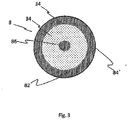
- a detachment level 8 is shown, the areas with different defect concentrations 82, 84, 86 has. It is conceivable that a plurality of regions with different defect concentrations form a release plane 8, wherein it is also conceivable that the defects 34 in the release plane 8 are distributed substantially or exactly uniformly over the surface.
- the different defect concentrations can be of the same size or different in size.
- a first increased defect concentration represents a crack initiation concentration 82, which is preferably generated in the region of the edge or extending to the edge or adjacent to the edge.
- a crack guidance concentration 84 may be formed such that the crack separating the solid-state layer 4 from the solid 2 can be controlled or controlled.
- a center concentration 86 can be generated, which preferably allows a very flat surface in the region of the center of the solid 2.
- the crack guide concentration 84 is partially or completely annular or enclosing and thus preferably encloses sections and more preferably completely the center of the solid 2 and the solid layer 4. It is also conceivable that the crack guidance concentration 84 in a starting from the edge of the solid second and gradually decreases in the direction of the center of the solid 2 or continuously or fluently. Furthermore, it is conceivable. the crack guidance concentration 84 is formed in a ribbon-like and homogeneous or substantially or exactly homogeneous manner.
Landscapes
- Engineering & Computer Science (AREA)
- Microelectronics & Electronic Packaging (AREA)
- Power Engineering (AREA)
- Manufacturing & Machinery (AREA)
- Computer Hardware Design (AREA)
- General Physics & Mathematics (AREA)
- Physics & Mathematics (AREA)
- Condensed Matter Physics & Semiconductors (AREA)
- Chemical & Material Sciences (AREA)
- Electromagnetism (AREA)
- Medicinal Chemistry (AREA)
- Polymers & Plastics (AREA)
- Health & Medical Sciences (AREA)
- Chemical Kinetics & Catalysis (AREA)
- Organic Chemistry (AREA)
- Compositions Of Macromolecular Compounds (AREA)
- Mechanical Treatment Of Semiconductor (AREA)
- Dicing (AREA)
- Processing Of Stones Or Stones Resemblance Materials (AREA)
Applications Claiming Priority (4)
| Application Number | Priority Date | Filing Date | Title |
|---|---|---|---|
| DE102014114456 | 2014-10-06 | ||
| DE102015103118.3A DE102015103118A1 (de) | 2014-10-06 | 2015-03-04 | Splitting-Verfahren und Verwendung eines Materials in einem Splitting-Verfahren |
| EP15781323.9A EP3186824B1 (fr) | 2014-10-06 | 2015-10-06 | Procédé de division et utilisation d'un matériau dans un procédé de division |
| PCT/EP2015/072990 WO2016055443A1 (fr) | 2014-10-06 | 2015-10-06 | Procédé de division et utilisation d'un matériau dans un procédé de division |
Related Parent Applications (2)
| Application Number | Title | Priority Date | Filing Date |
|---|---|---|---|
| EP15781323.9A Division EP3186824B1 (fr) | 2014-10-06 | 2015-10-06 | Procédé de division et utilisation d'un matériau dans un procédé de division |
| EP15781323.9A Division-Into EP3186824B1 (fr) | 2014-10-06 | 2015-10-06 | Procédé de division et utilisation d'un matériau dans un procédé de division |
Publications (1)
| Publication Number | Publication Date |
|---|---|
| EP3361495A1 true EP3361495A1 (fr) | 2018-08-15 |
Family
ID=55531253
Family Applications (2)
| Application Number | Title | Priority Date | Filing Date |
|---|---|---|---|
| EP15781323.9A Active EP3186824B1 (fr) | 2014-10-06 | 2015-10-06 | Procédé de division et utilisation d'un matériau dans un procédé de division |
| EP18163583.0A Pending EP3361495A1 (fr) | 2014-10-06 | 2015-10-06 | Matériau hybride en polymère, son procédé de fabrication ainsi que son utilisation et procédé de fractionnement |
Family Applications Before (1)
| Application Number | Title | Priority Date | Filing Date |
|---|---|---|---|
| EP15781323.9A Active EP3186824B1 (fr) | 2014-10-06 | 2015-10-06 | Procédé de division et utilisation d'un matériau dans un procédé de division |
Country Status (7)
| Country | Link |
|---|---|
| US (1) | US10229835B2 (fr) |
| EP (2) | EP3186824B1 (fr) |
| JP (1) | JP6820853B2 (fr) |
| KR (1) | KR102554020B1 (fr) |
| CN (1) | CN107004569B (fr) |
| DE (1) | DE102015103118A1 (fr) |
| WO (1) | WO2016055443A1 (fr) |
Cited By (1)
| Publication number | Priority date | Publication date | Assignee | Title |
|---|---|---|---|---|
| EP3433876B1 (fr) * | 2016-03-24 | 2023-09-13 | Siltectra GmbH | Un procédé de division |
Families Citing this family (2)
| Publication number | Priority date | Publication date | Assignee | Title |
|---|---|---|---|---|
| DE102016105616A1 (de) * | 2016-03-24 | 2017-09-28 | Siltectra Gmbh | Polymer-Hybrid-Material, dessen Verwendung in einem Splitting-Verfahren und Verfahren zur Herstellung des Polymer-Hybrid-Materials |
| EP3551373A1 (fr) * | 2016-12-12 | 2019-10-16 | Siltectra GmbH | Procédé d'amincissement de couches de solides pourvues de composants |
Citations (6)
| Publication number | Priority date | Publication date | Assignee | Title |
|---|---|---|---|---|
| DE19640594A1 (de) | 1996-10-01 | 1998-04-02 | Siemens Ag | Licht-induzierte Grenzflächenzersetzung zur Strukturierung und Trennung von Halbleitermaterialien |
| US20010038093A1 (en) * | 1999-09-17 | 2001-11-08 | Honeywell International Inc. | Interface materials and methods of production and use thereof |
| US20050222323A1 (en) * | 2002-04-11 | 2005-10-06 | Xiao-Qi Zhou | Thermally conductive coating compositions, methods of production and uses thereof |
| WO2010072675A2 (fr) * | 2008-12-23 | 2010-07-01 | Pfeffer, Christian | Procédé de production de minces couches libres de matériaux semi-conducteurs avec des surfaces structurées |
| DE102012001620A1 (de) | 2012-01-30 | 2013-08-01 | Siltectra Gmbh | Verfahren zur Herstellung von dünnen Platten aus Werkstoffen geringer Duktilität mittels temperaturinduzierter mechanischer Spannung unter Verwendung von vorgefertigten Polymer-Folien |
| US20140038392A1 (en) * | 2012-02-26 | 2014-02-06 | Solexel, Inc. | Systems and methods for laser splitting and device layer transfer |
Family Cites Families (12)
| Publication number | Priority date | Publication date | Assignee | Title |
|---|---|---|---|---|
| US6238596B1 (en) | 1999-03-09 | 2001-05-29 | Johnson Matthey Electronics, Inc. | Compliant and crosslinkable thermal interface materials |
| JP2001044144A (ja) | 1999-08-03 | 2001-02-16 | Tokyo Seimitsu Co Ltd | 半導体チップの製造プロセス |
| JP2006184504A (ja) | 2004-12-27 | 2006-07-13 | Canon Inc | 記録材判別装置および画像形成装置 |
| JP5117692B2 (ja) | 2006-07-14 | 2013-01-16 | ルネサスエレクトロニクス株式会社 | 半導体装置の製造方法 |
| KR101546112B1 (ko) | 2007-11-02 | 2015-08-20 | 프레지던트 앤드 펠로우즈 오브 하바드 칼리지 | 폴리머를 갖는 기판의 열처리에 의한 자립 고체상태 층의 제조 |
| JP5506026B2 (ja) | 2009-07-03 | 2014-05-28 | ユニオンケミカー株式会社 | 感圧転写型粘着テープ |
| WO2011018989A1 (fr) * | 2009-08-11 | 2011-02-17 | 浜松ホトニクス株式会社 | Dispositif dusinage laser et procédé dusinage laser |
| US8748296B2 (en) * | 2011-06-29 | 2014-06-10 | International Business Machines Corporation | Edge-exclusion spalling method for improving substrate reusability |
| JP2014049537A (ja) | 2012-08-30 | 2014-03-17 | Disco Abrasive Syst Ltd | ウェーハの加工方法 |
| JP2014072452A (ja) * | 2012-09-28 | 2014-04-21 | Fujifilm Corp | 半導体装置製造用仮接合層、積層体、及び、半導体装置の製造方法。 |
| JP6188051B2 (ja) * | 2012-12-25 | 2017-08-30 | 国立研究開発法人産業技術総合研究所 | 部品製造方法、接合剥離装置、および複合キャリア |
| DE102014013107A1 (de) | 2013-10-08 | 2015-04-09 | Siltectra Gmbh | Neuartiges Waferherstellungsverfahren |
-
2015
- 2015-03-04 DE DE102015103118.3A patent/DE102015103118A1/de not_active Withdrawn
- 2015-10-06 EP EP15781323.9A patent/EP3186824B1/fr active Active
- 2015-10-06 KR KR1020177012177A patent/KR102554020B1/ko active IP Right Grant
- 2015-10-06 US US15/516,781 patent/US10229835B2/en active Active
- 2015-10-06 EP EP18163583.0A patent/EP3361495A1/fr active Pending
- 2015-10-06 CN CN201580062196.XA patent/CN107004569B/zh active Active
- 2015-10-06 WO PCT/EP2015/072990 patent/WO2016055443A1/fr active Application Filing
- 2015-10-06 JP JP2017537017A patent/JP6820853B2/ja active Active
Patent Citations (6)
| Publication number | Priority date | Publication date | Assignee | Title |
|---|---|---|---|---|
| DE19640594A1 (de) | 1996-10-01 | 1998-04-02 | Siemens Ag | Licht-induzierte Grenzflächenzersetzung zur Strukturierung und Trennung von Halbleitermaterialien |
| US20010038093A1 (en) * | 1999-09-17 | 2001-11-08 | Honeywell International Inc. | Interface materials and methods of production and use thereof |
| US20050222323A1 (en) * | 2002-04-11 | 2005-10-06 | Xiao-Qi Zhou | Thermally conductive coating compositions, methods of production and uses thereof |
| WO2010072675A2 (fr) * | 2008-12-23 | 2010-07-01 | Pfeffer, Christian | Procédé de production de minces couches libres de matériaux semi-conducteurs avec des surfaces structurées |
| DE102012001620A1 (de) | 2012-01-30 | 2013-08-01 | Siltectra Gmbh | Verfahren zur Herstellung von dünnen Platten aus Werkstoffen geringer Duktilität mittels temperaturinduzierter mechanischer Spannung unter Verwendung von vorgefertigten Polymer-Folien |
| US20140038392A1 (en) * | 2012-02-26 | 2014-02-06 | Solexel, Inc. | Systems and methods for laser splitting and device layer transfer |
Cited By (1)
| Publication number | Priority date | Publication date | Assignee | Title |
|---|---|---|---|---|
| EP3433876B1 (fr) * | 2016-03-24 | 2023-09-13 | Siltectra GmbH | Un procédé de division |
Also Published As
| Publication number | Publication date |
|---|---|
| KR20170067819A (ko) | 2017-06-16 |
| WO2016055443A1 (fr) | 2016-04-14 |
| JP6820853B2 (ja) | 2021-01-27 |
| US20180233373A1 (en) | 2018-08-16 |
| EP3186824A1 (fr) | 2017-07-05 |
| CN107004569A (zh) | 2017-08-01 |
| DE102015103118A1 (de) | 2016-04-07 |
| EP3186824B1 (fr) | 2018-05-16 |
| CN107004569B (zh) | 2022-01-18 |
| JP2017531925A (ja) | 2017-10-26 |
| KR102554020B1 (ko) | 2023-07-11 |
| US10229835B2 (en) | 2019-03-12 |
Similar Documents
| Publication | Publication Date | Title |
|---|---|---|
| EP3055098B1 (fr) | Procédé de fabrication de tranches de silicium | |
| EP3280577B1 (fr) | Procédé de fabrication de tranches avec economie de materiaux | |
| EP3055447B1 (fr) | Création d'un point de départ de fissure ou d'un guide de fissuration afin de permettre un meilleur détachement d'une couche de solide à partir d'un solide | |
| EP3055448B1 (fr) | Procédé de production combiné permettant de séparer plusieurs couches de solide minces à partir d'un solide épais | |
| DE102014002600A1 (de) | Kombiniertes Waferherstellungsverfahren mit Laserbehandlung und temperaturinduzierten Spannungen | |
| DE102015004603A1 (de) | Kombiniertes Waferherstellungsverfahren mit Laserbehandlung und temperaturinduzierten Spannungen | |
| EP3186824B1 (fr) | Procédé de division et utilisation d'un matériau dans un procédé de division | |
| EP3147068B1 (fr) | Nouveau procédé de fabrication de tranches | |
| EP3137657B1 (fr) | Procédé combiné de fabrication de corps solides par traitement au laser et tensions thermo-induites pour la production de corps solides tridimensionnels | |
| WO2018108938A1 (fr) | Procédé d'amincissement de couches de solides pourvues de composants | |
| EP3433876B1 (fr) | Un procédé de division | |
| DE102017010284A1 (de) | Verfahren zum Dünnen von mit Bauteilen versehenen Festkörperschichten | |
| EP3201941B1 (fr) | Procédé combiné de fabrication de tranches au moyen d'une couche réceptrice pourvue de trous | |
| DE102016014821A1 (de) | Verfahren zum Dünnen von mit Bauteilen versehenen Festkörperschichten | |
| EP3201944B1 (fr) | Procédé combiné de fabrication de tranches au moyen d'une couche réceptrice à plusieurs constituants | |
| DE102016105616A1 (de) | Polymer-Hybrid-Material, dessen Verwendung in einem Splitting-Verfahren und Verfahren zur Herstellung des Polymer-Hybrid-Materials | |
| EP3608048B1 (fr) | Procédé de fabrication d'éléments de corps solide au moyen du traitement laser et de contraintes induites par la température | |
| WO2018108909A1 (fr) | Procédé d'amélioration de la qualité de surface d'une surface résultant d'une propagation de fissures |
Legal Events
| Date | Code | Title | Description |
|---|---|---|---|
| PUAI | Public reference made under article 153(3) epc to a published international application that has entered the european phase |
Free format text: ORIGINAL CODE: 0009012 |
|
| STAA | Information on the status of an ep patent application or granted ep patent |
Free format text: STATUS: THE APPLICATION HAS BEEN PUBLISHED |
|
| AC | Divisional application: reference to earlier application |
Ref document number: 3186824 Country of ref document: EP Kind code of ref document: P |
|
| AK | Designated contracting states |
Kind code of ref document: A1 Designated state(s): AL AT BE BG CH CY CZ DE DK EE ES FI FR GB GR HR HU IE IS IT LI LT LU LV MC MK MT NL NO PL PT RO RS SE SI SK SM TR |
|
| STAA | Information on the status of an ep patent application or granted ep patent |
Free format text: STATUS: REQUEST FOR EXAMINATION WAS MADE |
|
| 17P | Request for examination filed |
Effective date: 20190214 |
|
| RBV | Designated contracting states (corrected) |
Designated state(s): AL AT BE BG CH CY CZ DE DK EE ES FI FR GB GR HR HU IE IS IT LI LT LU LV MC MK MT NL NO PL PT RO RS SE SI SK SM TR |
|
| STAA | Information on the status of an ep patent application or granted ep patent |
Free format text: STATUS: REQUEST FOR EXAMINATION WAS MADE |
|
| STAA | Information on the status of an ep patent application or granted ep patent |
Free format text: STATUS: EXAMINATION IS IN PROGRESS |
|
| 17Q | First examination report despatched |
Effective date: 20210219 |
|
| STAA | Information on the status of an ep patent application or granted ep patent |
Free format text: STATUS: EXAMINATION IS IN PROGRESS |