EP3055447B1 - Création d'un point de départ de fissure ou d'un guide de fissuration afin de permettre un meilleur détachement d'une couche de solide à partir d'un solide - Google Patents
Création d'un point de départ de fissure ou d'un guide de fissuration afin de permettre un meilleur détachement d'une couche de solide à partir d'un solide Download PDFInfo
- Publication number
- EP3055447B1 EP3055447B1 EP14781229.1A EP14781229A EP3055447B1 EP 3055447 B1 EP3055447 B1 EP 3055447B1 EP 14781229 A EP14781229 A EP 14781229A EP 3055447 B1 EP3055447 B1 EP 3055447B1
- Authority
- EP
- European Patent Office
- Prior art keywords
- solid
- state body
- layer
- defects
- crack
- Prior art date
- Legal status (The legal status is an assumption and is not a legal conclusion. Google has not performed a legal analysis and makes no representation as to the accuracy of the status listed.)
- Active
Links
- 239000007787 solid Substances 0.000 title description 139
- 230000001976 improved effect Effects 0.000 title description 2
- 238000005336 cracking Methods 0.000 title 1
- 230000007547 defect Effects 0.000 claims description 52
- 230000005855 radiation Effects 0.000 claims description 39
- 238000000034 method Methods 0.000 claims description 35
- 229920000642 polymer Polymers 0.000 claims description 30
- 238000000926 separation method Methods 0.000 claims description 21
- 230000008569 process Effects 0.000 claims description 19
- 229910052710 silicon Inorganic materials 0.000 claims description 16
- 239000010703 silicon Substances 0.000 claims description 16
- 238000007669 thermal treatment Methods 0.000 claims description 10
- 239000002826 coolant Substances 0.000 claims description 9
- 238000001816 cooling Methods 0.000 claims description 8
- 230000006641 stabilisation Effects 0.000 claims description 6
- 238000011105 stabilization Methods 0.000 claims description 6
- 239000004205 dimethyl polysiloxane Substances 0.000 claims description 5
- 230000009477 glass transition Effects 0.000 claims description 5
- 229920000435 poly(dimethylsiloxane) Polymers 0.000 claims description 5
- 229910010293 ceramic material Inorganic materials 0.000 claims description 3
- 229910052751 metal Inorganic materials 0.000 claims description 3
- 239000002184 metal Substances 0.000 claims description 3
- GYHNNYVSQQEPJS-UHFFFAOYSA-N Gallium Chemical compound [Ga] GYHNNYVSQQEPJS-UHFFFAOYSA-N 0.000 claims description 2
- 229910052733 gallium Inorganic materials 0.000 claims description 2
- 235000013870 dimethyl polysiloxane Nutrition 0.000 claims 1
- CXQXSVUQTKDNFP-UHFFFAOYSA-N octamethyltrisiloxane Chemical compound C[Si](C)(C)O[Si](C)(C)O[Si](C)(C)C CXQXSVUQTKDNFP-UHFFFAOYSA-N 0.000 claims 1
- 238000004987 plasma desorption mass spectroscopy Methods 0.000 claims 1
- 230000035882 stress Effects 0.000 description 40
- 239000000463 material Substances 0.000 description 38
- 235000012431 wafers Nutrition 0.000 description 32
- 230000000977 initiatory effect Effects 0.000 description 23
- 239000000758 substrate Substances 0.000 description 22
- 150000002500 ions Chemical class 0.000 description 21
- XUIMIQQOPSSXEZ-UHFFFAOYSA-N Silicon Chemical compound [Si] XUIMIQQOPSSXEZ-UHFFFAOYSA-N 0.000 description 15
- 238000004519 manufacturing process Methods 0.000 description 15
- 238000010438 heat treatment Methods 0.000 description 8
- 239000000919 ceramic Substances 0.000 description 7
- 230000001939 inductive effect Effects 0.000 description 6
- 229910052594 sapphire Inorganic materials 0.000 description 6
- 239000010980 sapphire Substances 0.000 description 6
- 230000003313 weakening effect Effects 0.000 description 6
- IJGRMHOSHXDMSA-UHFFFAOYSA-N Atomic nitrogen Chemical compound N#N IJGRMHOSHXDMSA-UHFFFAOYSA-N 0.000 description 4
- 230000006378 damage Effects 0.000 description 4
- 230000000694 effects Effects 0.000 description 4
- 230000008901 benefit Effects 0.000 description 3
- 238000003776 cleavage reaction Methods 0.000 description 3
- 238000004581 coalescence Methods 0.000 description 3
- 238000005520 cutting process Methods 0.000 description 3
- 230000032798 delamination Effects 0.000 description 3
- 238000009826 distribution Methods 0.000 description 3
- 238000002844 melting Methods 0.000 description 3
- 230000008018 melting Effects 0.000 description 3
- 230000007017 scission Effects 0.000 description 3
- 239000000126 substance Substances 0.000 description 3
- JBRZTFJDHDCESZ-UHFFFAOYSA-N AsGa Chemical compound [As]#[Ga] JBRZTFJDHDCESZ-UHFFFAOYSA-N 0.000 description 2
- 229910001218 Gallium arsenide Inorganic materials 0.000 description 2
- 229910052782 aluminium Inorganic materials 0.000 description 2
- XAGFODPZIPBFFR-UHFFFAOYSA-N aluminium Chemical compound [Al] XAGFODPZIPBFFR-UHFFFAOYSA-N 0.000 description 2
- PNEYBMLMFCGWSK-UHFFFAOYSA-N aluminium oxide Inorganic materials [O-2].[O-2].[O-2].[Al+3].[Al+3] PNEYBMLMFCGWSK-UHFFFAOYSA-N 0.000 description 2
- JNDMLEXHDPKVFC-UHFFFAOYSA-N aluminum;oxygen(2-);yttrium(3+) Chemical compound [O-2].[O-2].[O-2].[Al+3].[Y+3] JNDMLEXHDPKVFC-UHFFFAOYSA-N 0.000 description 2
- 230000008859 change Effects 0.000 description 2
- 229910052593 corundum Inorganic materials 0.000 description 2
- 239000013078 crystal Substances 0.000 description 2
- 229910021419 crystalline silicon Inorganic materials 0.000 description 2
- 238000000354 decomposition reaction Methods 0.000 description 2
- 238000002513 implantation Methods 0.000 description 2
- 230000001965 increasing effect Effects 0.000 description 2
- 238000005468 ion implantation Methods 0.000 description 2
- 239000007788 liquid Substances 0.000 description 2
- 238000011068 loading method Methods 0.000 description 2
- 229910052757 nitrogen Inorganic materials 0.000 description 2
- 229910052756 noble gas Inorganic materials 0.000 description 2
- 239000002245 particle Substances 0.000 description 2
- 230000000737 periodic effect Effects 0.000 description 2
- 230000009467 reduction Effects 0.000 description 2
- 239000004065 semiconductor Substances 0.000 description 2
- HBMJWWWQQXIZIP-UHFFFAOYSA-N silicon carbide Chemical compound [Si+]#[C-] HBMJWWWQQXIZIP-UHFFFAOYSA-N 0.000 description 2
- 229910010271 silicon carbide Inorganic materials 0.000 description 2
- 239000002210 silicon-based material Substances 0.000 description 2
- 230000008646 thermal stress Effects 0.000 description 2
- 238000012876 topography Methods 0.000 description 2
- 239000012780 transparent material Substances 0.000 description 2
- 229910001845 yogo sapphire Inorganic materials 0.000 description 2
- 229910019901 yttrium aluminum garnet Inorganic materials 0.000 description 2
- WHXSMMKQMYFTQS-UHFFFAOYSA-N Lithium Chemical compound [Li] WHXSMMKQMYFTQS-UHFFFAOYSA-N 0.000 description 1
- 229910000577 Silicon-germanium Inorganic materials 0.000 description 1
- 229910000831 Steel Inorganic materials 0.000 description 1
- RTAQQCXQSZGOHL-UHFFFAOYSA-N Titanium Chemical compound [Ti] RTAQQCXQSZGOHL-UHFFFAOYSA-N 0.000 description 1
- 239000000443 aerosol Substances 0.000 description 1
- 229910002113 barium titanate Inorganic materials 0.000 description 1
- JRPBQTZRNDNNOP-UHFFFAOYSA-N barium titanate Chemical compound [Ba+2].[Ba+2].[O-][Ti]([O-])([O-])[O-] JRPBQTZRNDNNOP-UHFFFAOYSA-N 0.000 description 1
- 230000004888 barrier function Effects 0.000 description 1
- AOWKSNWVBZGMTJ-UHFFFAOYSA-N calcium titanate Chemical compound [Ca+2].[O-][Ti]([O-])=O AOWKSNWVBZGMTJ-UHFFFAOYSA-N 0.000 description 1
- 238000006243 chemical reaction Methods 0.000 description 1
- 239000000084 colloidal system Substances 0.000 description 1
- 238000010276 construction Methods 0.000 description 1
- 230000007423 decrease Effects 0.000 description 1
- 239000002612 dispersion medium Substances 0.000 description 1
- 238000005516 engineering process Methods 0.000 description 1
- 238000005530 etching Methods 0.000 description 1
- 229910000154 gallium phosphate Inorganic materials 0.000 description 1
- 239000007789 gas Substances 0.000 description 1
- 229910052732 germanium Inorganic materials 0.000 description 1
- GNPVGFCGXDBREM-UHFFFAOYSA-N germanium atom Chemical compound [Ge] GNPVGFCGXDBREM-UHFFFAOYSA-N 0.000 description 1
- 239000011521 glass Substances 0.000 description 1
- 229910052743 krypton Inorganic materials 0.000 description 1
- DNNSSWSSYDEUBZ-UHFFFAOYSA-N krypton atom Chemical compound [Kr] DNNSSWSSYDEUBZ-UHFFFAOYSA-N 0.000 description 1
- 229910052745 lead Inorganic materials 0.000 description 1
- 229910052744 lithium Inorganic materials 0.000 description 1
- GQYHUHYESMUTHG-UHFFFAOYSA-N lithium niobate Chemical compound [Li+].[O-][Nb](=O)=O GQYHUHYESMUTHG-UHFFFAOYSA-N 0.000 description 1
- 229910052749 magnesium Inorganic materials 0.000 description 1
- 239000011777 magnesium Substances 0.000 description 1
- 230000007246 mechanism Effects 0.000 description 1
- 239000000155 melt Substances 0.000 description 1
- 238000004377 microelectronic Methods 0.000 description 1
- 239000000203 mixture Substances 0.000 description 1
- 230000004048 modification Effects 0.000 description 1
- 238000012986 modification Methods 0.000 description 1
- 229910003465 moissanite Inorganic materials 0.000 description 1
- 229910021421 monocrystalline silicon Inorganic materials 0.000 description 1
- 229910052754 neon Inorganic materials 0.000 description 1
- GKAOGPIIYCISHV-UHFFFAOYSA-N neon atom Chemical compound [Ne] GKAOGPIIYCISHV-UHFFFAOYSA-N 0.000 description 1
- 150000002835 noble gases Chemical class 0.000 description 1
- 230000010355 oscillation Effects 0.000 description 1
- 238000013082 photovoltaic technology Methods 0.000 description 1
- 229910021420 polycrystalline silicon Inorganic materials 0.000 description 1
- -1 polydimethylsiloxane Polymers 0.000 description 1
- 229920005591 polysilicon Polymers 0.000 description 1
- 230000008092 positive effect Effects 0.000 description 1
- 239000010453 quartz Substances 0.000 description 1
- 229910052761 rare earth metal Inorganic materials 0.000 description 1
- 150000002910 rare earth metals Chemical class 0.000 description 1
- 230000000717 retained effect Effects 0.000 description 1
- VYPSYNLAJGMNEJ-UHFFFAOYSA-N silicon dioxide Inorganic materials O=[Si]=O VYPSYNLAJGMNEJ-UHFFFAOYSA-N 0.000 description 1
- 229910052709 silver Inorganic materials 0.000 description 1
- 239000004332 silver Substances 0.000 description 1
- 239000007858 starting material Substances 0.000 description 1
- 239000010959 steel Substances 0.000 description 1
- 238000000859 sublimation Methods 0.000 description 1
- 230000008022 sublimation Effects 0.000 description 1
- 239000002887 superconductor Substances 0.000 description 1
- 238000010897 surface acoustic wave method Methods 0.000 description 1
- 230000000930 thermomechanical effect Effects 0.000 description 1
- 229910052724 xenon Inorganic materials 0.000 description 1
- FHNFHKCVQCLJFQ-UHFFFAOYSA-N xenon atom Chemical compound [Xe] FHNFHKCVQCLJFQ-UHFFFAOYSA-N 0.000 description 1
- 229910021521 yttrium barium copper oxide Inorganic materials 0.000 description 1
Images

Classifications
-
- C—CHEMISTRY; METALLURGY
- C30—CRYSTAL GROWTH
- C30B—SINGLE-CRYSTAL GROWTH; UNIDIRECTIONAL SOLIDIFICATION OF EUTECTIC MATERIAL OR UNIDIRECTIONAL DEMIXING OF EUTECTOID MATERIAL; REFINING BY ZONE-MELTING OF MATERIAL; PRODUCTION OF A HOMOGENEOUS POLYCRYSTALLINE MATERIAL WITH DEFINED STRUCTURE; SINGLE CRYSTALS OR HOMOGENEOUS POLYCRYSTALLINE MATERIAL WITH DEFINED STRUCTURE; AFTER-TREATMENT OF SINGLE CRYSTALS OR A HOMOGENEOUS POLYCRYSTALLINE MATERIAL WITH DEFINED STRUCTURE; APPARATUS THEREFOR
- C30B33/00—After-treatment of single crystals or homogeneous polycrystalline material with defined structure
- C30B33/06—Joining of crystals
-
- B—PERFORMING OPERATIONS; TRANSPORTING
- B23—MACHINE TOOLS; METAL-WORKING NOT OTHERWISE PROVIDED FOR
- B23K—SOLDERING OR UNSOLDERING; WELDING; CLADDING OR PLATING BY SOLDERING OR WELDING; CUTTING BY APPLYING HEAT LOCALLY, e.g. FLAME CUTTING; WORKING BY LASER BEAM
- B23K26/00—Working by laser beam, e.g. welding, cutting or boring
- B23K26/36—Removing material
- B23K26/40—Removing material taking account of the properties of the material involved
-
- B—PERFORMING OPERATIONS; TRANSPORTING
- B23—MACHINE TOOLS; METAL-WORKING NOT OTHERWISE PROVIDED FOR
- B23K—SOLDERING OR UNSOLDERING; WELDING; CLADDING OR PLATING BY SOLDERING OR WELDING; CUTTING BY APPLYING HEAT LOCALLY, e.g. FLAME CUTTING; WORKING BY LASER BEAM
- B23K26/00—Working by laser beam, e.g. welding, cutting or boring
- B23K26/50—Working by transmitting the laser beam through or within the workpiece
- B23K26/53—Working by transmitting the laser beam through or within the workpiece for modifying or reforming the material inside the workpiece, e.g. for producing break initiation cracks
-
- B—PERFORMING OPERATIONS; TRANSPORTING
- B28—WORKING CEMENT, CLAY, OR STONE
- B28D—WORKING STONE OR STONE-LIKE MATERIALS
- B28D1/00—Working stone or stone-like materials, e.g. brick, concrete or glass, not provided for elsewhere; Machines, devices, tools therefor
- B28D1/005—Cutting sheet laminae in planes between faces
-
- B—PERFORMING OPERATIONS; TRANSPORTING
- B28—WORKING CEMENT, CLAY, OR STONE
- B28D—WORKING STONE OR STONE-LIKE MATERIALS
- B28D1/00—Working stone or stone-like materials, e.g. brick, concrete or glass, not provided for elsewhere; Machines, devices, tools therefor
- B28D1/22—Working stone or stone-like materials, e.g. brick, concrete or glass, not provided for elsewhere; Machines, devices, tools therefor by cutting, e.g. incising
- B28D1/221—Working stone or stone-like materials, e.g. brick, concrete or glass, not provided for elsewhere; Machines, devices, tools therefor by cutting, e.g. incising by thermic methods
-
- B—PERFORMING OPERATIONS; TRANSPORTING
- B28—WORKING CEMENT, CLAY, OR STONE
- B28D—WORKING STONE OR STONE-LIKE MATERIALS
- B28D5/00—Fine working of gems, jewels, crystals, e.g. of semiconductor material; apparatus or devices therefor
-
- H—ELECTRICITY
- H01—ELECTRIC ELEMENTS
- H01L—SEMICONDUCTOR DEVICES NOT COVERED BY CLASS H10
- H01L21/00—Processes or apparatus adapted for the manufacture or treatment of semiconductor or solid state devices or of parts thereof
- H01L21/70—Manufacture or treatment of devices consisting of a plurality of solid state components formed in or on a common substrate or of parts thereof; Manufacture of integrated circuit devices or of parts thereof
- H01L21/71—Manufacture of specific parts of devices defined in group H01L21/70
- H01L21/76—Making of isolation regions between components
- H01L21/762—Dielectric regions, e.g. EPIC dielectric isolation, LOCOS; Trench refilling techniques, SOI technology, use of channel stoppers
- H01L21/7624—Dielectric regions, e.g. EPIC dielectric isolation, LOCOS; Trench refilling techniques, SOI technology, use of channel stoppers using semiconductor on insulator [SOI] technology
- H01L21/76251—Dielectric regions, e.g. EPIC dielectric isolation, LOCOS; Trench refilling techniques, SOI technology, use of channel stoppers using semiconductor on insulator [SOI] technology using bonding techniques
- H01L21/76254—Dielectric regions, e.g. EPIC dielectric isolation, LOCOS; Trench refilling techniques, SOI technology, use of channel stoppers using semiconductor on insulator [SOI] technology using bonding techniques with separation/delamination along an ion implanted layer, e.g. Smart-cut, Unibond
-
- B—PERFORMING OPERATIONS; TRANSPORTING
- B23—MACHINE TOOLS; METAL-WORKING NOT OTHERWISE PROVIDED FOR
- B23K—SOLDERING OR UNSOLDERING; WELDING; CLADDING OR PLATING BY SOLDERING OR WELDING; CUTTING BY APPLYING HEAT LOCALLY, e.g. FLAME CUTTING; WORKING BY LASER BEAM
- B23K2103/00—Materials to be soldered, welded or cut
- B23K2103/50—Inorganic material, e.g. metals, not provided for in B23K2103/02 – B23K2103/26
Definitions
- the present invention relates to a method for producing solid layers according to the subject matter of claim 1.
- wafers In many technical areas (e.g. microelectronics or photovoltaic technology), materials such as silicon, germanium or sapphire are often used in the form of thin disks and plates (so-called wafers). As a standard, such wafers are currently produced from an ingot by sawing, which results in relatively large material losses (“kerf loss”). Since the starting material used is often very expensive, there are strong efforts to produce such wafers using less material and therefore more efficiently and cost-effectively.
- kerf loss material losses
- kerf-free wafering processes that do without conventional sawing and can, for example, split thin wafers directly from a thicker workpiece by using temperature-induced stresses. This includes, in particular, procedures such as those in PCT/US2008/012140 ( WO 2009/061 353 A2 ) and PCT/EP2009/067539 are described, where a polymer layer applied to the workpiece is used to generate these stresses.
- the polymer layer has a coefficient of thermal expansion that is approximately two orders of magnitude higher than that of the workpiece.
- a relatively high modulus of elasticity can be achieved of the polymer layer can be achieved, so that sufficiently large tensions can be induced in the polymer layer-workpiece layer system by cooling to enable the wafer to be separated from the workpiece.
- the wafers produced usually have larger fluctuations in thickness, with the spatial thickness distribution often showing a pattern with four-fold symmetry.
- TTV total thickness variation
- H + ions at 150 keV are introduced into a monocrystalline silicon plate by means of ion implantation.
- the H + ions are introduced into the silicon plate in such a controlled manner that they essentially come to rest on a defined plane within the plate.
- the dose of the implanted H + ions is greater than 10 16 cm -2 , which causes coalescence of the introduced ions as a result of heating the silicon plate to a temperature of greater than 500 ° C, which leads to a separation of the plane of the introduced Ions adjacent parts of the silicon plate leads.
- This process is very cost-intensive and complex because an extremely complex and expensive ion gun with appropriate control devices must be provided. Furthermore, the implantation of the ions takes a long time due to the high dose. Furthermore, heating the silicon plate requires a large amount of energy and prevents electrical components that are damaged at such high temperatures from being placed on the silicon plate before heating.
- the WO 2013 / 126 927 A2 describes the delamination (splitting) of a component layer from a donor substrate.
- a laser step forms cavities in a horizontal first zone of the donor substrate and polysilicon zones in a second horizontal zone of the donor substrate. In the first zone, the donor substrate is under tensile stress. In the adjacent second zone, the donor substrate is under compressive stress.
- a delamination process separates the device layer from the donor substrate along a laser cleavage surface that extends between the first zone and the second zone.
- the delamination process includes a thermal treatment that induces mechanical stress in the donor substrate, wherein during the thermal treatment the donor substrate is fixed by a substrate holder and/or a wafer handler.
- the thermal treatment may include heating and/or cooling of the donor substrate, for example by directing a jet of liquid nitrogen onto the surface of the donor substrate.
- the thermal treatment increases the intrinsic mechanical stress in the donor substrate and thus supports crack propagation along the laser gap surface.
- the thermal treatment increases the mechanical stress between the parts of the donor substrate modified by the previous laser irradiation and the unmodified parts of the donor substrate, thereby exploiting an intrinsic CTE mismatch between the zone with polycrystalline material and the zone with voids.
- the publication WO 2007/087 354 A2 describes the horizontal splitting of a silicon ingot starting from a notch on the edge of the ingot.
- a laser beam is focused at a distance from the planar surface of the ingot, initially near the tip of the notch and later at increasing horizontal distances from the notch.
- the laser beam locally heats the silicon crystal.
- the thermomechanical stresses induced thereby ensure that the crack spreads horizontally into the interior of the ingot until a disk is finally detached from the silicon ingot.
- the crystalline structure of the silicon is retained.
- the publication US 2007 / 0 249 140 A1 refers to the production of solar cells from crystalline silicon material.
- a stress-inducing material is applied to the surface of a mother substrate.
- a lower sub-layer of the stress-inducing material contains, for example, silver and an upper sub-layer aluminum. When heated, the stress-inducing layer peels off a thin partial layer of the mother substrate.
- the publication WO 2008/082 723 A2 also refers to the manufacture of solar cells from crystalline silicon material. Using a laser, thermal energy is introduced along a cleavage plane of an initial substrate. The temperature gradient between highly heated silicon and less heated silicon induces mechanical stress (fracture stress), which is carried along the cleavage plane.
- the present invention relates to a method for producing solid-state layers according to claim 1.
- the method according to the invention for producing solid-state layers comprises at least the steps: providing a solid for separating at least one solid-state layer, generating defects by means of at least one radiation source, in particular a laser, in the internal structure of the solid to specify a crack initiation point, starting from which the solid layer is separated from the solid and/or generating defects by means of at least the radiation source, in particular a laser, in the internal structure of the solid to specify a crack path along which the solid layer is separated from the solid, arranging a receiving layer for holding the solid layer on the solid, thermally applying heat to the receiving layer to generate, in particular mechanically, stresses in the solid, the stresses causing a crack starting from the crack initiation point and/or along the crack guide spreads over the solid body, which separates the solid layer from the solid body.
- This solution is advantageous because the crack path can be specified in a significantly improved manner, which means that significantly evener solid layers or solid layers with a significantly
- a laser radiation directed onto the wafer surface for example a UV laser, is applied locally relative to the wafer to produce the crack initiation point and/or guided in the circumferential direction of the solid to produce the crack guidance.
- the resulting notches preferably have a width of 2-5 ⁇ m and a depth of preferably 3-10 ⁇ m.
- the cutting speed is preferably in the range from 50 to 70 mm/s.
- the depth of the notches can be, for example, less than 1/10 or less than 1/100 or less than 1/1000 of the material thickness or the diameter of the solid or the width of the solid. Compared to mechanical scoring, the process speed is significantly higher.
- thermally induced stress differences are generated in the area of the defects or the notch, which cause one or more separation cracks that cut through the flat material starting from the tips of the notch.
- the thermal stress difference is induced by, for example, guiding a second laser radiation, for example a CO2 laser, over the notch or the area of the defects (thermal compressive stress), which is followed by a coolant jet (thermal tensile stress).
- the second laser radiation heats the material in the notch or the material in the area of the defects to just below the melting temperature and is quenched by the following coolant jet consisting of a water-air mixture (aerosol) or a cooled gas. This process preferably happens at a speed of 300 to 400 mm/s.
- the selection of the lasers for the first and second laser radiation as well as their process parameters depends on the material. While the laser for the first laser radiation and the process parameters acting here (in particular laser power, pulse regime and the speed of the relative movement) is preferably selected so that the material in the affected area melts and is expelled, the laser for the second laser radiation and the ones acting here Process parameters are preferably selected so that the material is only heated to approximately the melting temperature.
- Different lasers as well as the same laser can be used.
- the different heating can be achieved by using lasers with different wavelengths that are absorbed to different extents by the material.
- the beam geometry of the radiation spot of the laser radiation striking the surface or radiation density distribution in the radiation spot can be changed to generate the two laser radiations with different effects. Varying the laser power or the pulse regime can also achieve the desired effect.
- the invention is not tied to the notch being produced using a laser.
- creating the notch using a laser is an advantage in order to carry out the cutting using just one technology.
- the positive effects of the invention are essentially brought about by the fact that in a method according to the invention, instead of a necessary initial crack on each starting edge, which is carried out by scoring, there is a notch or a weakening of the material caused by defects in the area of the desired crack initiation point or along the entire desired Parting line or crack propagation line is generated.
- the notch could also be created mechanically or by etching.
- the type of production of the notch is not crucial, but rather the fact that such a notch or material weakening or strength weakening is introduced or created in the area of the crack initiation point or along a crack guide in order to either start from the tips of the notch, to cause a crack in the solid or to create a defined location or area through the weakening of the material or reduction in strength, which is torn or in which a crack in the solid begins and / or spreads in a defined manner. It is therefore conceivable that the defects are not created to create a notch, but rather to cause a local weakening of the material.
- the material structure can be changed through energy input or the material can be doped locally in a targeted manner by ion implantation in order to change the material properties in such a way that the critical fracture stress in the crack initiation point and/or along the crack path is reduced.
- the areas of the solid in which the defects were generated are subjected to thermal stress in such a way that local compressive stresses arise, with further thermal exposure taking place after the production of the compressive stresses to generate local tensile stresses, whereby the different thermal impacts on the solids enter the area of the defects.
- This embodiment is advantageous because a partial crack in the solid has already been caused, the accuracy or flatness of which is extremely high.
- the defects are preferably introduced partially and preferably completely in the circumferential direction of the solid. It is conceivable that defects are generated in the solid body in the circumferential direction of the separation plane on more, exactly or less than 10, 20, 30, 40, 50, 60, 70, 80 or 90 percent of the circumference.
- the solid is heated by means of a laser to generate the compressive stresses in the area of the defects and is cooled by means of a coolant jet to generate the tensile stresses.
- a laser to generate the compressive stresses in the area of the defects
- a coolant jet to generate the tensile stresses.
- the stresses for detaching the solid layer are generated by the thermal impact on the receiving layer, i.e. a polymer layer.
- the thermal exposure represents a cooling of the recording layer or polymer layer to or below 10 ° C and particularly preferably below 0 ° C and more preferably below -10 ° C.
- the cooling of the polymer layer is most preferably carried out in such a way that at least part of the polymer layer, which preferably consists of PDMS, undergoes a glass transition.
- the cooling can be a cooling to below -100 ° C, which can be achieved, for example, using liquid nitrogen.
- the polymer layer contracts depending on the temperature change and/or undergoes a glass transition and transfers the resulting forces to the solid, whereby mechanical stresses can be generated in the solid, which lead to the initiation of a crack and/or to the propagation of cracks Crack initially spreads along the first separation plane to split off the solid layer.
- the solid is arranged on a holding layer for holding the solid, wherein the holding layer is arranged on a first flat surface portion of the solid, wherein the first flat surface portion of the solid is spaced from a second flat surface portion of the solid, wherein the polymer layer is arranged on the second flat surface portion and wherein the release plane is aligned parallel to the first flat surface portion and/or the second flat surface portion or is generated parallel.
- This embodiment is advantageous because the solid is arranged at least in sections and preferably completely between the holding layer and the polymer layer, whereby the stresses for crack generation or crack propagation can be introduced into the solid by means of one of these layers or by means of both layers.
- At least or exactly one radiation source is configured to provide the radiation to be introduced into the solid in such a way that the rays emitted by it produce the defects at predetermined locations within the solid.
- This embodiment is advantageous because defects in the solid can be produced extremely precisely by means of a radiation source, in particular by means of a laser.
- the solid has silicon and/or gallium or perovskite and the polymer layer and/or the holding layer consist at least partially and preferably completely or more than 75% of polydimethylsiloxane (PDMS), with the holding layer on one at least partially flat surface of a stabilization device is arranged, which at least partially consists of at least one metal.
- the stabilization device is preferably a plate, in particular a plate that has or consists of aluminum. This embodiment is advantageous because the solid body is defined or held firmly by the stabilization device and the holding layer, whereby the stresses can be generated very precisely in the solid body.
- the stresses in the solid body can be adjusted or generated in such a way that the initiation of cracks and/or the propagation of cracks can be controlled to produce a topography of the surface resulting in the plane of the crack.
- the stresses are therefore preferably different in different areas of the solid body, preferably at least at times highly producible.
- This embodiment is advantageous because the topography of the solid layer produced or separated can be advantageously influenced by controlling the initiation of the crack and/or the course of the crack.
- the solid preferably has a material or a combination of materials from one of the main groups 3, 4 and 5 of the periodic table of elements, such as Si, SiC, SiGe, Ge, GaAs, InP, GaN, Al2O3 (sapphire), AIN.
- the solid particularly preferably has a combination of elements occurring in the third and fifth groups of the periodic table.
- Conceivable materials or material combinations are, for example, gallium arsenide, silicon, silicon carbide, etc.
- the solid can have a ceramic (e.g.
- Al2O3 - aluminum oxide or consist of a ceramic; preferred ceramics are, for example, perovskite ceramics (such as Pb, O, Ti /Zr-containing ceramics) in general and lead-magnesium niobates, barium titanate, lithium titanate, yttrium aluminum garnet, in particular yttrium aluminum garnet crystals for solid-state laser applications, SAW ceramics (surface acoustic wave), such as lithium niobate, gallium orthophosphate, Quartz, calcium titanate, etc. in particular.
- the solid body therefore preferably has a semiconductor material or a ceramic material or particularly preferably the solid body consists of at least one semiconductor material or a ceramic material.
- the solid body has a transparent material or partially consists or is made of a transparent material, such as sapphire.
- a transparent material such as sapphire.
- Other materials that can be used as solid-state materials alone or in combination with another material include, for example, "wide band gap" materials, InAISb, high-temperature superconductors, in particular rare earth cuprates (e.g. YBa2Cu3O7).
- the defects for generating the crack initiation point and/or for generating the crack guidance and/or for defining or establishing a separation plane are caused by the introduction of ions into the solid, the ions being provided by means of the radiation source .
- At least or exactly one radiation source is provided for providing the ions to be introduced into the solid, the radiation source being aligned in such a way that the ions emitted by it penetrate into the solid.
- the radiation source preferably serves to provide H + ions or noble gas ions, such as the substances neon, krypton and xenon, with the ions of the remaining noble gases not mentioned also can be used.
- the ions of the aforementioned substances and/or other substances are used separately or in combination.
- the radiation source is adjusted such that the ions emitted by it penetrate into the solid body to a defined depth, in particular ⁇ 100 ⁇ m, to create the separation plane.
- the separation plane is preferably formed parallel to an outer and preferably flat surface of the solid.
- the release plane is formed within the solid body at a distance of less than 100 micrometers and preferably less than 50 micrometers and particularly preferably less than or equal to 20, 10, 5 or 2 micrometers from the flat surface of the solid body.
- the solid is exposed to a predetermined dose of ions, the predetermined dose being less than 5+10 15 cm -2 or less than 10 15 cm -2 or less than 10 14 cm -2 or less than 10 13 cm -2 .
- the predetermined dose being less than 5+10 15 cm -2 or less than 10 15 cm -2 or less than 10 14 cm -2 or less than 10 13 cm -2 .
- the solid body is tempered in such a way that coalescence of the ions introduced into the solid body is prevented.
- Coalescence generally refers to the merging of colloidal particles.
- Colloids are particles or ions that are finely distributed in the dispersion medium (solid body).
- This embodiment is advantageous because not only temperature-stable solids, but also temperature-critical solids or solids with temperature-critical components, such as electronic components, which operate at temperatures of greater than 50 ° C or greater than 100 ° C or greater than 200 ° C or greater than 300 ° C or greater than 400°C or greater than 500°C can be processed.
- a defined starting point and/or a defined crack guide at a desired height are created laterally on the edge of the wafer.
- the process can be combined in any way with the other two processes, which cause surface damage to the layer.
- the advantage of the process is that there is not only damage to the material, but also a real crack seed, which then serves as the starting point for the crack when mechanical stress is generated by the cooling of a layer attached to the solid body. This lowers the energy barrier dramatic for the start of the crack, enables a defined crack start at a definable height (e.g. exactly at the height of the damage layer introduced) or when applied to a cold sample it could be used as a crack initialization as part of the splitting device.
- the invention further relates to a wafer which is produced by a method according to one of the claims.
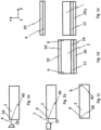
- a solid body 2 is shown, into which defects 34 are introduced by means of a radiation source 18, which is preferably a laser or an ion gun, or in which defects 34 are generated.
- the rays 6 from the radiation source 18 preferably strike the solid body 2 from the side and penetrate into it.
- a voltage inducing device 19 for generating voltages in the solid body 2 in order to cause a crack in the solid body 2 in the area of the defects 34 generated.
- the voltage inducing device 19 preferably consists of a heating device, in particular a laser, in particular a CO2 laser, and a coolant device, in particular for providing a coolant jet.
- the heating device in particular the laser
- the area in which defects were previously created is heated so that compressive stresses arise in this area.
- the initially heated area is preferably cooled again, whereby tensile stresses are generated in the area.
- the so thermally induced Stresses cause the solid body 2 to break into the area of the defects, which creates a crack 9.
- the reference number 40 indicates, on the one hand, that the crack 9 represents a crack initiation point. Furthermore, the reference number 42 indicates that the outline 9 can additionally or alternatively also represent a crack guide. It is therefore conceivable that only one crack guide 42 or only one crack initiation point 40 is generated, with both preferably being generated at the same time or with a time delay.
- the crack initiation point 40 extends in the circumferential direction of the solid body 2 significantly less than the crack guide 42, significantly less can be understood, for example, as exact, less or more than 1/10, 1/100, 1/1000 of the extent of the crack guide, whereby also any fractions in between are conceivable.
- Fig. 1d are on the solid body 2 analogous to the statements regarding.
- Fig. 2b different layers 10, 12, 20 arranged. Individual or all of the layers 10, 12, 20 are then exposed to thermal loading, through which stresses are introduced into the solid body 2. Due to the generated cracks 9, ie the crack initiation point 40 and/or the crack guide 42, the crack is introduced into a separation plane in a defined manner, whereby the solid layer 4 is separated from the solid 2 (cf. Fig. 1e ).
- the present invention therefore relates to a method for producing solid layers and preferably comprises the steps: Providing a solid body 2 for separating at least one solid body layer 4, generating defects by means of at least one radiation source 18, in particular a laser, in the internal structure of the solid body to specify a crack initiation point from which the solid body layer 4 is separated from the solid body 2 and/or generating of defects by means of at least the radiation source 18, in particular a laser, in the internal structure of the solid body 2 to specify a crack path along which the solid body layer 4 is separated from the solid body 2, arranging a recording layer 10 for holding the solid body layer 4 to the solid body 2, thermal Acting on the receiving layer 10 to generate, in particular mechanically, stresses in the solid body 2, the stresses causing a crack to propagate starting from the crack initiation point and/or along the crack guide in the solid body 2, which separates the solid body layer 4 from the solid body 2.
- a solid body 2 or a substrate is shown, which is arranged in the area of a radiation source 18, in particular a laser or an ion gun.
- the solid body 2 preferably has a first flat surface portion 14 and a second flat surface portion 16, wherein the first flat surface portion 14 is preferably aligned essentially or exactly parallel to the second flat surface portion 16.
- the first flat surface portion 14 and the second flat surface portion 16 preferably delimit the solid body 2 in a Y direction, which is preferably oriented vertically or perpendicularly.
- the flat surface portions 14 and 16 preferably each extend in an XZ plane, the XZ plane preferably being oriented horizontally. Furthermore, it can be seen from this illustration that the radiation source 18 radiates steel 6 onto the solid body 2.
- the beams 6 penetrate a defined depth into the solid body 2 and create a defect at the respective position or at a predetermined position.
- the defects cause a weakening or modification of the solid structure, in particular a reduction in the breaking strength, which occurs on a level or essentially or exactly on a level that is referred to as the detachment level 8.
- the separation plane 8 can be generated before or after the creation of the crack initiation point 40 or the crack path 42.
- the defects that are introduced to create the crack initiation point 40 and/or the crack guide 42 are created before, during or after the creation or introduction of the defects to create the detachment plane 8.
- the defects for producing the crack initiation point 40 and/or the crack guide 42 are preferably generated on or in the separation plane 8.
- Fig. 2b a multi-layer arrangement is shown, wherein the solid body 2 contains the detachment plane 8 and is provided in the area of the first flat surface portion 14 with a holding layer 12, which in turn is preferably overlaid by a further layer 20, the further layer 20 preferably having a stabilization device, in particular a metal plate.
- a polymer layer 10 is preferably arranged on the second flat surface portion 16 of the solid body 2.
- the polymer layer 10 and/or the holding layer 12 preferably consist at least partially and particularly preferably completely of PDMS.
- Fig. 2c A state is shown after a crack has been initiated and subsequently cracked.
- the solid layer 4 adheres to the polymer layer 10 and is spaced or can be spaced apart from the remaining rest of the solid 2.
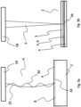
- FIG. 3a and 3b are examples of the in Fig. 2a shown generation of a detachment plane 8 by introducing defects into a solid 2 using light rays.
- a method for producing solid-state layers 4 includes at least the steps of providing a solid-state body 2 for separating at least one solid-state layer 4, of producing defects by means of at least one radiation source, in particular a laser, in the internal structure of the solid-state body to specify a Detachment plane, along which the solid layer is separated from the solid, and the thermal loading of a polymer layer 10 arranged on the solid 2 to generate, in particular mechanically, stresses in the solid 2, the stresses causing a crack in the solid 2 along the detachment plane 8 spreads, which separates the solid layer 4 from the solid 2, includes.
- Fig. 3a is shown schematically how defects 34 can be generated in a solid body 2, in particular for generating a separation plane 8, by means of a radiation source 18, in particular one or more lasers.
- the radiation source 18 emits radiation 6 with a first wavelength 30 and a second wavelength 32.
- the wavelengths 30, 32 are coordinated with one another or the distance between the radiation source 18 and the separation plane 8 to be generated is coordinated in such a way that the waves 30 , 32 meet essentially or exactly at the separation plane 8 in the solid body 2, whereby a defect is generated at the point of meeting 34 as a result of the energies of both waves 30, 32.
- the generation of defects can occur through different or combined decomposition mechanisms, such as sublimation or chemical reaction, whereby the decomposition can be initiated, for example, thermally and/or photochemically.
- a focused light beam 6 is shown, the focal point of which preferably lies in the separation plane 8. It is conceivable here that the light beam 6 is focused by one or more focusing bodies, in particular lenses (not shown).
- the solid body 2 is designed in multiple layers and preferably has a partially transparent or transparent substrate layer 3 or material layer, which preferably consists of sapphire or has sapphire.
- the light rays 6 pass through the substrate layer 3 onto the release plane 8, which is preferably formed by a sacrificial layer 5, the sacrificial layer 5 being acted upon by the radiation in such a way that thermally and/or a partial or complete destruction of the sacrificial layer 5 in the focal point or in the area of the focal point is effected photochemically. It is also conceivable that the defects for producing the release layer 8 are created in the area or exactly on an interface between two layers 3, 4.
- the solid-state layer 4 is produced on a carrier layer, in particular a substrate layer 3, and by means of one or more sacrificial layers 5 and/or by means of the generation of defects in an interface, in particular between the solid-state layer 4 and the carrier layer, a release plane 8 can be produced for detaching or separating the solid layer 4.
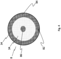
- a detachment plane 8 is shown, which has areas with different defect concentrations 82, 84, 86. It is conceivable here that a large number of areas with different defect concentrations form a detachment plane 8, it being also conceivable that the defects 34 in the detachment plane 8 are distributed essentially or exactly evenly over the surface.
- the different defect concentrations can have the same area or different sizes.
- a first increased defect concentration represents a crack initiation concentration 82, which is preferably generated in the area of the edge or extending towards the edge or adjacent to the edge.
- a crack guidance concentration 84 can be formed such that the crack separating the solid layer 4 from the solid 2 can be controlled or controlled.
- a center concentration 86 can additionally or alternatively be generated, which preferably enables a very flat surface in the area of the center of the solid 2.
- the crack guidance concentration 84 is partially or completely annular or enclosing and thus preferably partially and particularly preferably completely encloses the center of the solid 2 or the solid layer 4. It is also conceivable that the crack guidance concentration 84 is in one starting from the edge of the solid 2 and decreases gradually or steadily or smoothly towards the center of the solid body 2. Furthermore, it is conceivable that the crack guidance concentration 84 is band-like and homogeneous or essentially or exactly homogeneous.
Claims (7)
- Procédé de production de couches de corps solide comprenant au moins les stades :on se procure un corps (2) solide pour la séparation d'au moins une couche (4) de corps solide, dans lequel le corps (2) a une première partie (14) de surface plane et une deuxième partie (16) de surface plane,on produit des défauts (34), au moyen du rayonnement laser d'au moins un laser, dans la structure intérieure du corps (2) solide pour la prescription d'un guide de fissuration, le long duquel on sépare la couche (4) de corps solide du corps (2) solide et dans lequel, au moyen du au moins un laser ou d'une autre source de rayonnement, on produit, dans la structure intérieure du corps (2) solide, d'autres défauts (34) pour la prescription d'un plan (8) de détachement, le long duquel on sépare la couche (4) de corps solide du corps (2) solide,on met une couche (10) de polymère pour maintenir la couche (4) de corps solide sur le corps (2) solide, dans lequel on met la couche (10) de polymère sur la deuxième partie (16) de surface plane,on soumet à un traitement thermique la couche (10) de polymère, le traitement thermique représentant un refroidissement de la couche (10) de polymère à une température en-dessous de 10°C, dans lequel la couche (10) de polymère se contracte et/ou subit une transition à l'état vitreux et transmet les forces, qui se créent ainsi, au corps (2) solide, grâce à quoi on produit, dans le corps (2) solide des contraintes mécaniques et dans lequel, par les contraintes, se propagent, dans le corps (2) solide, le long du guide de fissuration, une fissure, qui sépare la couche (4) de corps solide du corps (2) solide.
- Procédé suivant la revendication 1, caractérisé
en ce que l'on traite thermiquement les parties du corps (2) solide, dans lesquelles les défauts (34) ont été produits pour prescrire un guide de fissuration, de manière à donner des contraintes de pression locales, dans lequel, après la production des contraintes de pression, on effectue un autre traitement thermique de production de contraintes de traction locales, dans lequel, par les traitements thermiques différents, le corps (2) solide se fend dans la partie des défauts (34) . - Procédé suivant la revendication 2, caractérisé
en ce que l'on chauffe le corps (2) solide pour la production des contraintes de pression dans la partie des défauts (34) au moyen d'un ou d'un autre laser et en ce que l'on refroidit le corps (2) solide pour la production des contraintes de traction au moyen d'un jet de fluide de refroidissement. - Procédé suivant l'une des revendications précédentes,
caractérisé
en ce que le au moins un laser est configuré de manière à ce que les rayons (6), par lui émis, produisent les défauts (34) en des emplacements déterminés à l'avance au sein du corps (2) solide. - Procédé suivant l'une des revendications précédentes,
caractérisé
en ce que l'on met le corps (2) solide sur une couche (12) de maintien pour le maintien du corps (2) solide, dans lequel on met la couche (12) de maintien sur la première partie (14) de surface plane du corps (2) solide, dans lequel la première partie (14) de surface plane du corps (2) solide est à distance de la deuxième partie (16) de surface plane du corps (2) solide, dans lequel on met, sur la deuxième partie (16) de surface plane, la couche (10) de polymère et dans lequel on oriente le plan (8) de détachement parallèlement à la première partie (14) de surface plane et/ou à la deuxième partie (16) de surface plane. - Procédé suivant l'une des revendications précédentes,
caractérisé
en ce que le corps (2) solide comporte du silicium et/ou du gallium et/ou un matériau céramique et la couche de polymère et/ou la couche (12) de maintien est constituée au moins en partie de PDMS, dans lequel la couche (12) de maintien est mise sur une surface plane au moins par endroits d'un dispositif (20) de stabilisation, qui est constitué au moins en partie d'au moins un métal. - Procédé suivant l'une des revendications précédentes,
caractérisé
en ce que l'on refroidit la couche (10) de polymère, jusqu'à ce qu'au moins une partie de la couche (10) de polymère passe à l'état vitreux.
Applications Claiming Priority (2)
| Application Number | Priority Date | Filing Date | Title |
|---|---|---|---|
| DE201310016682 DE102013016682A1 (de) | 2013-10-08 | 2013-10-08 | Erzeugung einer Rissauslösestelle oder einer Rissführung zum verbesserten Abspalten einer Festkörperschicht von einem Festkörper |
| PCT/EP2014/071509 WO2015052218A1 (fr) | 2013-10-08 | 2014-10-08 | Création d'un point de départ de fissure ou d'un guide de fissuration afin de permettre un meilleur détachement d'une couche de solide à partir d'un solide |
Publications (2)
| Publication Number | Publication Date |
|---|---|
| EP3055447A1 EP3055447A1 (fr) | 2016-08-17 |
| EP3055447B1 true EP3055447B1 (fr) | 2024-03-13 |
Family
ID=51662128
Family Applications (1)
| Application Number | Title | Priority Date | Filing Date |
|---|---|---|---|
| EP14781229.1A Active EP3055447B1 (fr) | 2013-10-08 | 2014-10-08 | Création d'un point de départ de fissure ou d'un guide de fissuration afin de permettre un meilleur détachement d'une couche de solide à partir d'un solide |
Country Status (4)
| Country | Link |
|---|---|
| EP (1) | EP3055447B1 (fr) |
| DE (1) | DE102013016682A1 (fr) |
| TW (1) | TW201523696A (fr) |
| WO (1) | WO2015052218A1 (fr) |
Families Citing this family (10)
| Publication number | Priority date | Publication date | Assignee | Title |
|---|---|---|---|---|
| CN107206544A (zh) | 2015-01-28 | 2017-09-26 | 西尔特克特拉有限责任公司 | 透明的并且高度稳定的显示屏保护件 |
| DE102015003369A1 (de) | 2015-03-16 | 2016-09-22 | Siltectra Gmbh | Transparenter und hochstabiler Displayschutz |
| DE102015006971A1 (de) | 2015-04-09 | 2016-10-13 | Siltectra Gmbh | Verfahren zum verlustarmen Herstellen von Mehrkomponentenwafern |
| US11130200B2 (en) * | 2016-03-22 | 2021-09-28 | Siltectra Gmbh | Combined laser treatment of a solid body to be split |
| DE102017010284A1 (de) * | 2017-11-07 | 2019-05-09 | Siltectra Gmbh | Verfahren zum Dünnen von mit Bauteilen versehenen Festkörperschichten |
| DE102017007585A1 (de) * | 2017-08-11 | 2019-02-14 | Siltectra Gmbh | Vorrichtung und Verfahren zum Beaufschlagen von Spannungserzeugungsschichten mit Druck zum verbesserten Führen eines Abtrennrisses |
| CN110769967A (zh) | 2017-04-20 | 2020-02-07 | 西尔特克特拉有限责任公司 | 用于打薄设有部件的固体层的方法 |
| JP7285067B2 (ja) | 2018-10-30 | 2023-06-01 | 浜松ホトニクス株式会社 | レーザ加工装置及びレーザ加工方法 |
| US11897056B2 (en) * | 2018-10-30 | 2024-02-13 | Hamamatsu Photonics K.K. | Laser processing device and laser processing method |
| WO2020090929A1 (fr) * | 2018-10-30 | 2020-05-07 | 浜松ホトニクス株式会社 | Appareil de traitement laser et procédé de traitement laser |
Citations (1)
| Publication number | Priority date | Publication date | Assignee | Title |
|---|---|---|---|---|
| WO2007087354A2 (fr) * | 2006-01-24 | 2007-08-02 | Baer Stephen C | Clivage de tranches à partir de cristaux de silicium |
Family Cites Families (9)
| Publication number | Priority date | Publication date | Assignee | Title |
|---|---|---|---|---|
| FR2681472B1 (fr) | 1991-09-18 | 1993-10-29 | Commissariat Energie Atomique | Procede de fabrication de films minces de materiau semiconducteur. |
| DE102005038027A1 (de) | 2005-08-06 | 2007-02-08 | Jenoptik Automatisierungstechnik Gmbh | Verfahren zum Durchtrennen von spröden Flachmaterialien |
| EP1863100A1 (fr) * | 2006-05-30 | 2007-12-05 | INTERUNIVERSITAIR MICROELEKTRONICA CENTRUM vzw (IMEC) | Méthode de production de substrats fin |
| JP5117692B2 (ja) | 2006-07-14 | 2013-01-16 | ルネサスエレクトロニクス株式会社 | 半導体装置の製造方法 |
| US7811900B2 (en) * | 2006-09-08 | 2010-10-12 | Silicon Genesis Corporation | Method and structure for fabricating solar cells using a thick layer transfer process |
| AU2008325223A1 (en) * | 2007-11-02 | 2009-05-14 | President And Fellows Of Harvard College | Production of free-standing solid state layers by thermal processing of substrates with a polymer |
| ES2418142T3 (es) | 2008-12-23 | 2013-08-12 | Siltectra Gmbh | Procedimiento para producir capas independientes delgadas de materiales en estado sólido con superficies estructuradas |
| AU2013222069A1 (en) * | 2012-02-26 | 2014-10-16 | Solexel, Inc. | Systems and methods for laser splitting and device layer transfer |
| DE102013007672A1 (de) * | 2013-05-03 | 2014-11-06 | Siltectra Gmbh | Verfahren und Vorrichtung zur Waferherstellung mit vordefinierter Bruchauslösestelle |
-
2013
- 2013-10-08 DE DE201310016682 patent/DE102013016682A1/de not_active Withdrawn
-
2014
- 2014-10-08 WO PCT/EP2014/071509 patent/WO2015052218A1/fr active Application Filing
- 2014-10-08 EP EP14781229.1A patent/EP3055447B1/fr active Active
- 2014-10-08 TW TW103135026A patent/TW201523696A/zh unknown
Patent Citations (1)
| Publication number | Priority date | Publication date | Assignee | Title |
|---|---|---|---|---|
| WO2007087354A2 (fr) * | 2006-01-24 | 2007-08-02 | Baer Stephen C | Clivage de tranches à partir de cristaux de silicium |
Also Published As
| Publication number | Publication date |
|---|---|
| WO2015052218A1 (fr) | 2015-04-16 |
| DE102013016682A1 (de) | 2015-04-09 |
| EP3055447A1 (fr) | 2016-08-17 |
| TW201523696A (zh) | 2015-06-16 |
Similar Documents
| Publication | Publication Date | Title |
|---|---|---|
| EP3055447B1 (fr) | Création d'un point de départ de fissure ou d'un guide de fissuration afin de permettre un meilleur détachement d'une couche de solide à partir d'un solide | |
| EP3055098B1 (fr) | Procédé de fabrication de tranches de silicium | |
| EP3055448B1 (fr) | Procédé de production combiné permettant de séparer plusieurs couches de solide minces à partir d'un solide épais | |
| EP3280577B1 (fr) | Procédé de fabrication de tranches avec economie de materiaux | |
| EP1924392B1 (fr) | Procede de separation de materiaux plats cassants a l'aide du laser le long d'une trace prealablement produite | |
| EP3313603B1 (fr) | Procédé pour guider le cheminement d'une fissure dans la zone marginale d'un substrat donneur | |
| EP3313604B1 (fr) | Procédé pour guider le cheminement d'une fissure dans la zone marginale d'un substrat donneur au moyen d'un faisceau laser incliné | |
| DE102014002600A1 (de) | Kombiniertes Waferherstellungsverfahren mit Laserbehandlung und temperaturinduzierten Spannungen | |
| EP3245665B1 (fr) | Procédé pour fabriquer une tranche irrégulière | |
| DE102015004603A1 (de) | Kombiniertes Waferherstellungsverfahren mit Laserbehandlung und temperaturinduzierten Spannungen | |
| EP3137657B1 (fr) | Procédé combiné de fabrication de corps solides par traitement au laser et tensions thermo-induites pour la production de corps solides tridimensionnels | |
| EP3147068B1 (fr) | Nouveau procédé de fabrication de tranches | |
| EP3186824B1 (fr) | Procédé de division et utilisation d'un matériau dans un procédé de division | |
| EP3201944B1 (fr) | Procédé combiné de fabrication de tranches au moyen d'une couche réceptrice à plusieurs constituants | |
| EP3201941B1 (fr) | Procédé combiné de fabrication de tranches au moyen d'une couche réceptrice pourvue de trous | |
| EP3608048B1 (fr) | Procédé de fabrication d'éléments de corps solide au moyen du traitement laser et de contraintes induites par la température | |
| DE102013016665A1 (de) | Kombiniertes Waferherstellungsverfahren mit lonenimplantation und temperaturinduzierten Spannungen | |
| WO2022096064A1 (fr) | Procédé et système de fabrication d'un substrat | |
| DE102016105616A1 (de) | Polymer-Hybrid-Material, dessen Verwendung in einem Splitting-Verfahren und Verfahren zur Herstellung des Polymer-Hybrid-Materials | |
| DE102014004574A1 (de) | Verfahren zur Herstellung von Festkörperschichten mittels lokaler Modifikation von Leit-Stütz-Struktur-Eigenschaften einer mehrschichtigen Anordnung |
Legal Events
| Date | Code | Title | Description |
|---|---|---|---|
| PUAI | Public reference made under article 153(3) epc to a published international application that has entered the european phase |
Free format text: ORIGINAL CODE: 0009012 |
|
| 17P | Request for examination filed |
Effective date: 20160506 |
|
| AK | Designated contracting states |
Kind code of ref document: A1 Designated state(s): AL AT BE BG CH CY CZ DE DK EE ES FI FR GB GR HR HU IE IS IT LI LT LU LV MC MK MT NL NO PL PT RO RS SE SI SK SM TR |
|
| AX | Request for extension of the european patent |
Extension state: BA ME |
|
| DAX | Request for extension of the european patent (deleted) | ||
| RAP1 | Party data changed (applicant data changed or rights of an application transferred) |
Owner name: SILTECTRA GMBH |
|
| RAP1 | Party data changed (applicant data changed or rights of an application transferred) |
Owner name: SILTECTRA GMBH |
|
| RAP1 | Party data changed (applicant data changed or rights of an application transferred) |
Owner name: SILTECTRA GMBH |
|
| STAA | Information on the status of an ep patent application or granted ep patent |
Free format text: STATUS: EXAMINATION IS IN PROGRESS |
|
| 17Q | First examination report despatched |
Effective date: 20190212 |
|
| STAA | Information on the status of an ep patent application or granted ep patent |
Free format text: STATUS: EXAMINATION IS IN PROGRESS |
|
| STAA | Information on the status of an ep patent application or granted ep patent |
Free format text: STATUS: EXAMINATION IS IN PROGRESS |
|
| GRAP | Despatch of communication of intention to grant a patent |
Free format text: ORIGINAL CODE: EPIDOSNIGR1 |
|
| STAA | Information on the status of an ep patent application or granted ep patent |
Free format text: STATUS: GRANT OF PATENT IS INTENDED |
|
| RIC1 | Information provided on ipc code assigned before grant |
Ipc: B23K 103/00 20060101ALN20231113BHEP Ipc: B23K 26/53 20140101ALI20231113BHEP Ipc: B28D 5/00 20060101ALI20231113BHEP Ipc: B28D 1/00 20060101ALI20231113BHEP Ipc: H01L 21/762 20060101ALI20231113BHEP Ipc: B28D 1/22 20060101ALI20231113BHEP Ipc: B23K 26/40 20140101ALI20231113BHEP Ipc: C30B 33/06 20060101AFI20231113BHEP |
|
| INTG | Intention to grant announced |
Effective date: 20231211 |
|
| GRAS | Grant fee paid |
Free format text: ORIGINAL CODE: EPIDOSNIGR3 |
|
| GRAA | (expected) grant |
Free format text: ORIGINAL CODE: 0009210 |
|
| STAA | Information on the status of an ep patent application or granted ep patent |
Free format text: STATUS: THE PATENT HAS BEEN GRANTED |
|
| P01 | Opt-out of the competence of the unified patent court (upc) registered |
Effective date: 20240116 |
|
| AK | Designated contracting states |
Kind code of ref document: B1 Designated state(s): AL AT BE BG CH CY CZ DE DK EE ES FI FR GB GR HR HU IE IS IT LI LT LU LV MC MK MT NL NO PL PT RO RS SE SI SK SM TR |
|
| REG | Reference to a national code |
Ref country code: GB Ref legal event code: FG4D Free format text: NOT ENGLISH |
|
| REG | Reference to a national code |
Ref country code: CH Ref legal event code: EP |
|
| REG | Reference to a national code |
Ref country code: DE Ref legal event code: R096 Ref document number: 502014016783 Country of ref document: DE |