EP3357150B1 - Bi-directional current sensing circuit - Google Patents
Bi-directional current sensing circuit Download PDFInfo
- Publication number
- EP3357150B1 EP3357150B1 EP16788279.4A EP16788279A EP3357150B1 EP 3357150 B1 EP3357150 B1 EP 3357150B1 EP 16788279 A EP16788279 A EP 16788279A EP 3357150 B1 EP3357150 B1 EP 3357150B1
- Authority
- EP
- European Patent Office
- Prior art keywords
- current
- circuit
- transistor
- current sensing
- terminal
- Prior art date
- Legal status (The legal status is an assumption and is not a legal conclusion. Google has not performed a legal analysis and makes no representation as to the accuracy of the status listed.)
- Active
Links
Images


Classifications
-
- G—PHYSICS
- G01—MEASURING; TESTING
- G01R—MEASURING ELECTRIC VARIABLES; MEASURING MAGNETIC VARIABLES
- G01R19/00—Arrangements for measuring currents or voltages or for indicating presence or sign thereof
- G01R19/0092—Measuring current only
-
- G—PHYSICS
- G05—CONTROLLING; REGULATING
- G05F—SYSTEMS FOR REGULATING ELECTRIC OR MAGNETIC VARIABLES
- G05F1/00—Automatic systems in which deviations of an electric quantity from one or more predetermined values are detected at the output of the system and fed back to a device within the system to restore the detected quantity to its predetermined value or values, i.e. retroactive systems
- G05F1/10—Regulating voltage or current
-
- H—ELECTRICITY
- H02—GENERATION; CONVERSION OR DISTRIBUTION OF ELECTRIC POWER
- H02M—APPARATUS FOR CONVERSION BETWEEN AC AND AC, BETWEEN AC AND DC, OR BETWEEN DC AND DC, AND FOR USE WITH MAINS OR SIMILAR POWER SUPPLY SYSTEMS; CONVERSION OF DC OR AC INPUT POWER INTO SURGE OUTPUT POWER; CONTROL OR REGULATION THEREOF
- H02M1/00—Details of apparatus for conversion
- H02M1/0003—Details of control, feedback or regulation circuits
- H02M1/0009—Devices or circuits for detecting current in a converter
-
- H—ELECTRICITY
- H02—GENERATION; CONVERSION OR DISTRIBUTION OF ELECTRIC POWER
- H02M—APPARATUS FOR CONVERSION BETWEEN AC AND AC, BETWEEN AC AND DC, OR BETWEEN DC AND DC, AND FOR USE WITH MAINS OR SIMILAR POWER SUPPLY SYSTEMS; CONVERSION OF DC OR AC INPUT POWER INTO SURGE OUTPUT POWER; CONTROL OR REGULATION THEREOF
- H02M3/00—Conversion of DC power input into DC power output
- H02M3/02—Conversion of DC power input into DC power output without intermediate conversion into AC
- H02M3/04—Conversion of DC power input into DC power output without intermediate conversion into AC by static converters
- H02M3/10—Conversion of DC power input into DC power output without intermediate conversion into AC by static converters using discharge tubes with control electrode or semiconductor devices with control electrode
- H02M3/145—Conversion of DC power input into DC power output without intermediate conversion into AC by static converters using discharge tubes with control electrode or semiconductor devices with control electrode using devices of a triode or transistor type requiring continuous application of a control signal
- H02M3/155—Conversion of DC power input into DC power output without intermediate conversion into AC by static converters using discharge tubes with control electrode or semiconductor devices with control electrode using devices of a triode or transistor type requiring continuous application of a control signal using semiconductor devices only
- H02M3/156—Conversion of DC power input into DC power output without intermediate conversion into AC by static converters using discharge tubes with control electrode or semiconductor devices with control electrode using devices of a triode or transistor type requiring continuous application of a control signal using semiconductor devices only with automatic control of output voltage or current, e.g. switching regulators
Definitions
- At least certain embodiments disclosed herein relate generally to electronic circuits, and more particularly to an improved bi-directional current sensing circuit and method.
- Power conversion circuitry is employed in many applications, such as in portable devices, which utilize an external power source to operate the device and/or to charge internal batteries of the device.
- the current drawn from a source may need to be limited according to specifications published for devices drawing power from the connection.
- USB universal serial bus
- portable devices may be limited to drawing at most 500 mA from a USB 2.0 connection.
- USB 3.0 connections are typically limited to drawing 900 mA of current.
- Power conversion circuitry provides power conversion with current limiting using current sensing.
- Current sensing circuitry may be important in various power conversion devices such as battery chargers, switched-mode chargers, power converters, voltage regulators, etc. Bi-directional current sensing is needed to monitor the current in such devices during forward current mode and reverse current mode. The sensed current information may then be used for regulating the forward or reverse currents in the device, and also for fuel gauging to compute charge transfer in and out of the battery.
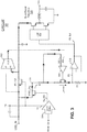
- FIG. 1 depicts an example of a conventional current sensing circuit utilized in a switched-mode charger according to the prior art.
- current sensing circuit 10 includes a USB_IN input power source configured to supply current to a buck/boost power regulator 120. More details can be found in document US2005151543 . Furthermore, a buck converter with an auxiliary current path and a current sensing path using MOSFETs is described in document US2014049238 .
- Circuit 10 includes two independent current sensing loops 102 and 104 for sensing current flow in both the forward and reverse directions respectively.
- current sensing circuit 10 includes a first independent loop 102 comprising a forward current sensing transistor SFET_Chg and a first operational amplifier 106, and a second independent loop 104 comprising a reverse current sensing transistor SFET_RB and a second operational amplifier 108.
- forward current flows into the device from the USB_IN input through a front porch FET transistor FP_FET and into the power regulator 120.
- the feedback loop 102 comprising the forward current sensing transistor SFET_Chg and operational amplifier 106 senses this current and is configured to equalize the drain-to-source voltage Vds of the power transistor FP_FET and the forward current sensing transistor SFET_Chg such that a sensed current "I1" will be a replica of the forward current.
- the feedback loop 104 comprising the reverse current sensing transistor SFET_RB and the operational amplifier 108 senses this reverse current and is configured to equalize the drain-to-source voltage Vds of the front porch transistor FP_FET and the reverse current sensing transistor SFET_RB such that a sensed current "12" will be a replica of the reverse current.
- Such circuits however occupy a significant amount of integrated die area, requiring two independent current sensing operational amplifiers 106 and 108, thereby increasing cost and design complexity.
- the invention is defined by the features of device claim 1 and corresponding method claim 10.
- the dependent claims recite advantageous embodiments of the invention.
- the circuit includes an area efficient bi-directional current sensing circuit using current sensing transistor gate control.
- the circuit includes a first current sensing transistor coupled between a current sensing circuit node and a first terminal of the power transistor.
- the first current sensing transistor can be configured to sense current conducting in the power transistor during a forward current mode of the circuit.
- the circuit further includes a second current sensing transistor coupled between the current sensing circuit node and a second terminal of the power transistor.
- the second current sensing transistor can be configured to sense current conducting in the power transistor during a reverse current mode of the circuit.
- the first and second current sensing transistors form a series connection in parallel with the power transistor.
- the circuit also includes a level shifter configured to provide complementary outputs depending on the mode of the circuit.
- the level shifter includes a first output coupled with the gate terminal of the first current sensing transistor to activate or deactivate the first current sensing transistor, and a second output coupled with the gate terminal of the second current sensing transistor to activate or deactivate the second current sensing transistor.
- the complementary outputs of the level shifter are configured to either turn on the first current sensing transistor and turn off the second current sensing transistor when the circuit is in forward current mode, or turn off the first current sensing transistor and turn on the second current sensing transistor when the circuit is in reverse current mode.
- the circuit comprises two current sensing loops including a first current sensing loop and a second current sensing loop. Only one of the current sensing loops is active at any one time based on the complementary outputs of the level shifter.
- the first current sensing loop comprises the first current sensing transistor coupled with an operational amplifier and the second current sensing loop comprises the second current sensing transistor coupled with the operational amplifier.
- the operational amplifier is configured to equalize voltage of the first terminal of the power transistor with a voltage of a corresponding terminal of the first current sensing transistor, or to equalize voltage of the second terminal of the power transistor with a voltage of a corresponding terminal of the second current sensing transistor.
- the circuit further comprises selection logic configured for selecting between sensing forward and reverse currents in the power transistor based on the mode of the circuit.
- the output of the selection logic will either be a signal mirroring the voltage at the first terminal of the power transistor during forward current mode, or a signal mirroring the voltage at the second terminal of the power transistor during reverse current mode.
- a method for sensing current conducting in a power transistor coupled between an input power supply and a power regulator comprises sensing current conducting in the power transistor during a forward current mode of the circuit at a first current sensing transistor coupled between a current sensing node of the circuit and a first terminal of the power transistor, and sensing current conducting in the power transistor during a reverse current mode of the circuit at a second current sensing transistor coupled between the current sensing node of the circuit and a second terminal of the power transistor.
- the first and second current sensing transistors form a series connection in parallel with the power transistor.
- the method further comprises providing complementary outputs from a level shifter depending on the mode of the circuit.
- the level shifter includes a first output coupled with the gate terminal of the first current sensing transistor to activate or deactivate the first current sensing transistor, and a second output coupled with the gate terminal of the second current sensing transistor to activate or deactivate the second current sensing transistor.
- the method activates only one of a first current sensing loop comprising the first current sensing transistor or a second current sensing loop comprising the second current sensing transistor at a time based on the complementary outputs of the level shifter by either turning on the first current sensing transistor and turning off the second current sensing transistor when the circuit is in forward current mode, or turning off the first current sensing transistor and turning on the second current sensing transistor when the circuit is in reverse current mode.
- the method further comprises selecting between sensing the forward current or the reverse current in the power transistor based on the mode of the circuit.
- the output of the selection logic will either be a signal mirroring the voltage of the first terminal of the power transistor during forward current mode, or a signal mirroring the voltage of the second terminal of the power transistor during reverse current mode.
- a circuit means for sensing current conducting in a power transistor coupled between an input power supply and a power regulator includes a means for sensing current conducting in the power transistor during a forward current mode of the circuit at a first current sensing transistor coupled between a current sensing circuit node and a first terminal of the power transistor, means for sensing current conducting in the power transistor during a reverse current mode of the circuit at a second current sensing transistor coupled between the current sensing circuit node and a second terminal of the power transistor, means for providing complementary outputs from a level shifter depending on the mode of the circuit, where the level shifter includes a first output coupled with the gate terminal of the first current sensing transistor to activate or deactivate the first current sensing transistor, and a second output coupled with the gate terminal of the second current sensing transistor to activate or deactivate the second current sensing transistor, and a means for activating only one of a first current sensing loop comprising the first current sensing transistor and a second current sensing loop comprising the second
- hardwired circuitry may be used independently or in combination with firmware or software instructions to implement the techniques described herein.
- the described functionality may be performed by custom hardware components containing hardwired logic for performing operations, or by any combination of hardware, firmware, and programmed computer components.
- the techniques described herein are not limited to any specific combination of hardware circuitry.
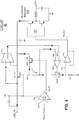
- FIG. 2 depicts an example circuit diagram of an embodiment of an area efficient bi-directional current sensing circuit using current sensing transistor gate control.
- Bi-directional current sensing circuit 20 includes a USB_IN power input configured for forward current and/or reverse current in a buck/boost regulator 220.
- the configuration of circuit 20 combines two uni-directional current sensing feedback loops into a single bi-directional current sensing circuit configured such that only one feedback loop is activated at any one time, and thus only one operational amplifier is required for current sensing in both the forward and reverse current directions.
- Circuit 20 is configured for sensing current in the forward and reverse current directions respectively.
- circuit 20 includes a front porch power transistor FP_FET, a forward current sensing transistor SFET_Chg, and a reverse current sensing transistor SFET_RB.
- Circuit 20 further comprises a multiplexer ("MUX") 202 for selecting between sensing the forward or reverse current based on the selected mode (mode_sel signal), a level shifter circuit 230 configured to turn on/off the forward and reverse current sensing transistors SFET_Chg and SFET_RB, respectively, and an operational amplifier 204 configured for sensing either the forward or reverse current and for equalizing the drain-to-source voltage Vds of the power transistor FP_FET with either the forward current sensing transistor SFET_Chg during forward current mode or the reverse boost current sensing transistor SFET_RB during reverse current mode.
- MUX multiplexer
- Circuit 20 also includes an operational amplifier 210 for buffering the feedback signal "FB" via resistor R1 to generate a buffered feedback voltage FB_Buf, which is supplied to the buck/boost regulator 220 via an input logic block 212.
- the buck/boost regulator 220 includes an inductor and a capacitor coupled with two input transistors.
- the buck/boost regulator 220 can be a voltage step down circuit adapted to step down the input power voltage supplied by USB_IN to a lower voltage "Vsys" for use by internal components of the system, such as a processor, microcontroller, etc.
- circuit techniques described herein are not limited to any particular semiconductor technology. It will be appreciated by persons of skill in the art that other types of transistors or equivalent devices may be used to implement the embodiments described herein. For example, embodiments may be implemented in transistor technologies including MOSFET, JFET, BJT, IGBT, GaAs, etc.
- transistor technologies including MOSFET, JFET, BJT, IGBT, GaAs, etc.
- the techniques described herein are based on an NFET transistor configuration, persons of skill in the art will appreciate that these techniques can also be based on a PFET transistor configuration as such is a simple design choice for a circuit designer.
- embodiments described herein include receiving power via a USB input, the embodiments are not so limited.
- the techniques described herein can be configured to receive input power from any type of power source, of which a USB input is only one example.
- the level shifter circuit 230 only activates one of the feedback loops at any given time interval depending on the mode_sel signal at the input.
- the gates of the current sensing transistors SFET_Chg and SFET_RB are driven by complementary output signals from the level shifter 230.
- the level shifter circuit 230 is configured to either turn on the forward current sensing transistor SFET_Chg and turn off the reverse boost current sensing transistor SFET_RB, or turn off the forward current sensing transistor SFET_Chg and turn on the reverse boost current sensing transistor SFET_RB.
- the level shifter 230 On its complementary outputs, the level shifter 230 provides an output voltage that swings between Vg (input voltage of circuit 20) and USB_IN - ⁇ V (USB_IN minus ⁇ V) depending on the state of the mode sel input signal. During forward current mode the state of the mode_sel signal can be set to 0, and during reverse current mode the state of the mode_sel signal can be set to 1.
- the level shifter 230 can be designed such that the output voltage Vg is high enough to turn on the current sensing transistors SFET_Chg or SFET_RB, and such that the output voltage USB_IN - ⁇ V is low enough to turn off the current sensing transistors SFET_Chg or SFET_RB.
- the level shifter 230 is described in more detail in FIG. 5 discussed below.
- the level shifter 230 outputs the gate voltage Vg to the input gate voltage Vg_Chg of the forward current sensing transistor SFET_Chg, and the level shifter 230 outputs USB_IN - ⁇ V to the input gate voltage Vg RB of the reverse boost current sensing transistor SFET_RB. This has the effect of turning on the current sensing transistor SFET_Chg and turning off the reverse boost current sensing transistor SFET_RB. Thus only SFET_Chg will be active and mirroring the forward current in forward current mode.
- the level shifter 230 outputs the gate voltage Vg to the input gate voltage Vg_RB of the reverse boost current sensing transistor SFET_RB and the level shifter 230 outputs USB_IN - ⁇ V to the input gate voltage Vg Chg of the forward current sensing transistor SFET_Chg.
- This has the effect of turning off the current sensing transistor SFET_Chg and turning on the reverse boost current sensing transistor SFET_RB.
- SFET_RB will be active and mirroring the reverse current in reverse boost mode.
- the circuit 20 is either sensing the forward current in forward current mode or sensing the reverse current in reverse boost mode.
- MUX 202 is configured to select between the drain and source terminals of the power transistor FP_FET in forward and reverse boost modes, respectively, depending on the state of the mode_sel signal. When the state of the mode_sel signal is set equal to 0, forward current mode is selected and the input s0 of MUX 202 will be active while input s1 is inactive. The s0 input of the MUX 202 will receive the signal from the drain terminal of the power transistor FP_FET.
- the state of the mode_sel signal is set equal to 1
- reverse current mode is selected and the s1 input of the MUX 202 will be active while the input s0 is inactive.
- the s1 input of the MUX 202 will receive the signal from the source terminal of the power transistor FP_FET.
- the output of MUX 202 will therefore either be a signal mirroring the voltage taken at the drain terminal of the power transistor FP_FET when forward current mode is selected, or a signal mirroring the voltage taken at the source terminal of FP_FET when the reverse boost mode is selected.
- the voltage signal at the output of the MUX 202 is provided to the negative (-) input 208 of the operational amplifier 204.
- the positive (+) input 206 of the operational amplifier is supplied with either the voltage signal taken at the current sensing node 203 via the forward current sensing transistor SFET_Chg during forward current mode, or the voltage signal taken at the current sensing node 203 via the reverse boost current sensing transistor SFET_RB during reverse current mode.
- the feedback loop comprising the forward current sensing transistor SFET_Chg and the operational amplifier 204 is configured to sense the forward current and to equalize the drain-to-source voltages Vds of FP_FET and SFET_Chg such that the sensed current I_sense mirrors the forward current.
- the feedback loop comprising the reverse current sensing transistor SFET_RB and the operational amplifier 204 is configured to sense the reverse current and to equalize the drain-to-source voltage Vds of FP_FET and SFET_RB such that the sensed current I_sense mirrors the reverse boost current.
- the sensed current I_sense is then provided as a feedback signal FB via resistor R1, and is buffered in operational amplifier 210 to produce a buffered feedback voltage FB_Buf.
- the buffered feedback FB_Buf can then be supplied to the input logic block 212 of the buck/boost regulator 220.
- the buck/boost regulator 220 can be configured to receive this feedback current and use it for regulating the forward and reverse currents in the device, and also for fuel gauging to compute charge transfer in and out of the device as discussed above.
- FIG. 3 depicts an equivalent circuit for the example circuit diagram embodiment of FIG. 2 during forward current mode.
- power flows in from USB_IN through the front porch power transistor FP_FET and into the buck/boost regulator 320.
- the mode_sel signal is set equal to 0 and therefore the output of the level shifter 330 supplies voltage signal Vg to the gate terminal of SFET_Chg to turn it on and supplies USB_IN - ⁇ V to the gate terminal of SFET_RB to turn it off.
- Forward current therefore flows through SFET_Chg and into the circuit as shown.
- the s0 input of MUX 302 is selected and the voltage signal Vd at the drain terminal of FP_FET is provided at the output of the MUX 302 and is supplied to the negative (-) input terminal 308 of the operational amplifier 304.
- the positive (+) input terminal 306 of the operational amplifier 304 is supplied with the voltage signal at the current sensing node 303 via transistor SFET_Chg.
- the feedback loop comprising the forward current sensing transistor SFET_Chg and the operational amplifier 304 is configured to sense the forward current and to equalize the drain-to-source voltages Vds of FP_FET and SFET_Chg such that the sensed current I_sense mirrors the forward current.
- Isense is then provided as a feedback voltage FB via resistor R1, and is buffered in operational amplifier 310 to produce a buffered feedback voltage FB_Buf.
- the buffered feedback FB_Buf can then be supplied to the input logic block 312 of the buck/boost regulator 320.
- FIG. 4 depicts an equivalent circuit for the example circuit diagram embodiment of FIG. 2 during reverse current.
- USB_IN in reverse current mode USB_IN is no longer supplying power to the circuit. Instead, the power accumulated in the buck/boost regulator 420 flows back from the buck/boost regulator 420 through the front porch power transistor FP_FET in the opposite direction.
- the mode sel signal is set equal to 1 and therefore the output of the level shifter 430 supplies voltage signal Vg to the gate terminal of SFET_RB to turn it on and supplies USB_IN - ⁇ V to the gate terminal of SFET_Chg to turn it off.
- Reverse boost current therefore flows through SFET_RB and into the circuit as shown.
- the s1 input of MUX 402 is selected and the voltage signal Vs at the source terminal of FP_FET is provided at the output of the MUX 402 and is supplied to the negative (-) input terminal 408 of the operational amplifier 404.
- the positive (+) input 406 of the operational amplifier 404 is supplied with the voltage signal at the current sensing node 403 via transistor SFET_RB.
- the feedback loop comprising the reverse boost current sensing transistor SFET_RB and the operational amplifier 404 is configured to sense the reverse current and to equalize the drain-to-source voltages Vds of FP_FET and SFET_RB such that the sensed current I_sense mirrors the reverse current.
- Isense is then provided as a feedback signal "FB" via resistor R1, and is buffered in operational amplifier 410 to produce a buffered feedback voltage FB_Buf.
- the buffered feedback voltage FBBuf can then be supplied to the input logic block 412 of the buck/boost regulator 420.
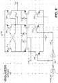
- FIG. 5 depicts an example circuit diagram of a level shifter circuit configuration.
- level shifter circuit 50 is configured to receive at its input (1) the mode_sel signal, (2) the USB_IN power signal, and (3) the input voltage signal Vg.
- the level shifter circuit is configured to supply complementary output voltages at outputs Out and Out_b.
- level shifter circuits are well known and the embodiments described herein are not limited to any particular circuit configuration so long as it provides complementary outputs where output Out is equal to Vg and output Out b is equal to USB_IN - ⁇ V, or output Out is equal to USB_IN - ⁇ V and output Out_b is equal to Vg.
- USB_IN - ⁇ V can be selected such that it is low enough to turn off the current sensing transistors SFET_Chg and SFET_RB of FIGs. 2-4 .
- mode sel input signal is inverted at inverting node 502 via a first inverter 540 and inverted again at (non-inverting) node 504 via a second inverter 541.
- the inverted mode_sel signal at the inverting node 502 is supplied to activate transistors 506 and 510 and the non-inverted mode_sel signal at the non-inverting node 504 is supplied to activate transistor 508.
- the state of the mode sel signal is set equal to 1. This in turn will set the state of inverting node 502 equal to 0 via inverter 540 and the noninverting node 504 equal to 1 via inverter 541. In this configuration, inverting node 502 will deactivate transistors 506 and 510 and noninverting node 504 will activate transistor 508.
- the output voltage at output Out_b will therefore be the input voltage Vg conducting down through transistors 518 and 520 and the output voltage at the output Out will be the voltage USB_IN minus the voltage ⁇ V of the conducting diode D3.
- the level shifter circuit 50 in this configuration is adapted to supply complementary voltages Vg and USB_IN at the outputs Out and Outb respectively during forward or reverse current mode.
- Other equivalent circuit configurations are possible.
- processes described below are exemplary in nature and are provided for illustrative purposes and not intended to limit the scope of the embodiments described herein to any particular example embodiment. For instance, processes in accordance with some embodiments may include or omit some or all of the operations described below, or may include steps in a different order than described herein. The particular processes described are not intended to be limited to any particular set of operations exclusive of all other potentially intermediate operations.
- the operations may be embodied in computer-executable code, which causes a general-purpose or special-purpose computer to perform certain functional operations. In other in stances, these operations may be performed by specific hardware components or hardwired circuitry, or by any combination of programmed computer components and custom hardware circuitry.
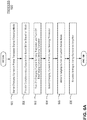
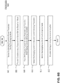
- FIG. 6A depicts an example flow chart of an embodiment of a process for sensing a forward current in a bi-directional current sensing circuit designed according to the techniques described herein with reference to FIG. 2 above.
- process 600 begins at operation 601 where the current conducting in the power transistor during forward current mode is sensed at a first current sensing transistor coupled between a current sensing node of the circuit and a first terminal of the power transistor.
- the first terminal of the power transistor is the source terminal.
- Process 600 continues at operation 602 by providing complementary outputs from a level shifter 230 depending on the selected mode of the circuit.
- the level shifter 230 includes a first output coupled with the gate terminal of the first current sensing transistor SFET_Chg to activate or deactivate the first current sensing transistor and a second output coupled with the gate terminal of a second current sensing transistor SFET_RB to activate or deactivate the second current sensing transistor.
- the circuit 20 comprises two current sensing loops but only one of the current sensing loops may be active at any one time based on the complementary outputs of the level shifter.
- Process 600 continues at operation 603 by turning on the first current sensing transistor SFET_Chg and turning off the second current sensing transistor SFET_RB via the complementary outputs of the level shifter 230 since the circuit is in forward current mode.
- the forward current conducting in the power transistor FP_FET sensed in the first current sensing transistor SFET_Chg is then selected (operation 604), and the forward current is mirrored in the current sensing node 203 of the circuit (operation 605).
- the voltage of the first terminal of the power transistor FP_FET can then be equalized with the voltage of the corresponding terminal of the first current sensing transistor SFET_Chg using an operational amplifier 204 (operation 606).
- Process 600 continues at FIG. 6B , which depicts an example flow chart of an embodiment of a process for sensing a reverse current in a bi-directional current sensing circuit designed according to the techniques described herein with reference to FIG. 2 above.
- process 600 continues at operation 607 where the current conducting in the power transistor FP_FET during reverse current mode is sensed at a second current sensing transistor SFET_RB coupled between the current sensing node 203 of the circuit and a second terminal of the power transistor.
- the second terminal of the power transistor FP_FET is the drain terminal.
- Process 600 continues at operation 608 by providing complementary outputs from a level shifter 230 depending on the mode of the circuit.
- the level shifter 230 includes a first output coupled with the gate terminal of the first current sensing transistor SFET_Chg to activate or deactivate the first current sensing transistor and a second output coupled with the gate terminal of a second current sensing transistor SFET_RB to activate or deactivate the second current sensing transistor.
- Process 600 continues at operation 609 by turning on the second current sensing transistor SFET_RB and turning off the first current sensing transistor SFET_Chg via the complementary outputs of the level shifter 230 since the circuit is in reverse current mode.
- the reverse current of the power transistor FP_FET sensed in the second current sensing transistor SFET_RB is then selected (operation 610) and the sensed current is mirrored in the current sensing node 203 of the circuit (operation 611).
- the voltage of the second terminal of the power transistor can then be equalized with the voltage of the corresponding terminal of the second current sensing transistor using the operational amplifier 204 (operation 612). This completes process 600 according to one example embodiment.
- the proposed solution is therefore capable of current sensing in applications with bi-directional power flow.
- the proposed solution provides an area-efficient bi-directional current sensing solution where current sensing is required in both the forward and reverse current directions.
- the embodiments described herein are adapted to combine two unidirectional current sensing feedback loops into a single bi-directional current sensing circuit.
- the circuit is configured to mirror the current flowing in the power transistor directly in a single mirroring stage in such a manner that multiple stages of indirect current mirroring and matching is not required.
- the current flowing in the forward or reverse current directions can be directly mirrored in either the forward current sensing transistor or the reverse current sensing transistor, respectively.
- the embodiments described herein can also reduce testing time during design parameter trimming. Since some design parameters vary with processing variations and may mismatch from chip to chip, chip-level measurements are required to trim them back to a desired value.
- the sense ratio can vary with mismatch and layout parasitics, for example. This can be corrected by trimming the resistor R1 such that the overall sense gain is corrected to the desired value for each individual chip during testing. Since the trimming is done on each chip, it adds to the cost and test time. But the bi-directional current sensing technique described herein only requires trimming in one direction, which improves accuracy and reduces testing time during manufacturing.
- DSP Digital Signal Processor
- ASIC Application Specific Integrated Circuit
- FPGA Field Programmable Gate Array
- a general purpose processor may be a microprocessor, but in the alternative, the processor may be any conventional processor, controller, microcontroller, or state machine, etc.
- a processor may also be implemented as a combination of computing devices, e.g., a combination of a DSP and a microprocessor, a plurality of microprocessors, one or more microprocessors in conjunction with a DSP core, or any other such configuration.
- a software module may reside in Random Access Memory (RAM), flash memory, Read Only Memory (ROM), Electrically Programmable ROM (EPROM), Electrically Erasable Programmable ROM (EEPROM), registers, hard disk, a removable disk, a CD-ROM, or any other form of storage medium known in the art.
- RAM Random Access Memory
- ROM Read Only Memory
- EPROM Electrically Programmable ROM
- EEPROM Electrically Erasable Programmable ROM
- registers hard disk, a removable disk, a CD-ROM, or any other form of storage medium known in the art.
- An exemplary storage medium is coupled with the processor such that the processor can read information from, and write information to, the storage medium. In the alternative, the storage medium may be integrated into the processor.
- Computer-readable media includes both computer storage media and communication media including any medium that facilitates transfer of a computer program from one place to another.
- a storage media may be any available media that can be accessed by a computer.
- such computer-readable media can comprise RAM, ROM, EEPROM, CD-ROM or other optical disk storage, magnetic disk storage or other magnetic storage devices, or any other medium that can be used to carry or store desired program code in the form of instructions or data structures and that can be accessed by a computer.
Landscapes
- Engineering & Computer Science (AREA)
- Physics & Mathematics (AREA)
- General Physics & Mathematics (AREA)
- Power Engineering (AREA)
- Electromagnetism (AREA)
- Radar, Positioning & Navigation (AREA)
- Automation & Control Theory (AREA)
- Dc-Dc Converters (AREA)
- Semiconductor Integrated Circuits (AREA)
- Amplifiers (AREA)
- Power Conversion In General (AREA)
- Measurement Of Current Or Voltage (AREA)
Applications Claiming Priority (2)
| Application Number | Priority Date | Filing Date | Title |
|---|---|---|---|
| US14/871,636 US9863982B2 (en) | 2015-09-30 | 2015-09-30 | Bi-directional current sensing circuit |
| PCT/US2016/055037 WO2017059378A1 (en) | 2015-09-30 | 2016-09-30 | Bi-directional current sensing circuit |
Publications (2)
| Publication Number | Publication Date |
|---|---|
| EP3357150A1 EP3357150A1 (en) | 2018-08-08 |
| EP3357150B1 true EP3357150B1 (en) | 2019-11-20 |
Family
ID=57209845
Family Applications (1)
| Application Number | Title | Priority Date | Filing Date |
|---|---|---|---|
| EP16788279.4A Active EP3357150B1 (en) | 2015-09-30 | 2016-09-30 | Bi-directional current sensing circuit |
Country Status (7)
| Country | Link |
|---|---|
| US (1) | US9863982B2 (enExample) |
| EP (1) | EP3357150B1 (enExample) |
| JP (1) | JP2018530298A (enExample) |
| KR (1) | KR20180063215A (enExample) |
| CN (1) | CN108141133A (enExample) |
| BR (1) | BR112018006418A2 (enExample) |
| WO (1) | WO2017059378A1 (enExample) |
Cited By (1)
| Publication number | Priority date | Publication date | Assignee | Title |
|---|---|---|---|---|
| TWI736190B (zh) * | 2020-03-23 | 2021-08-11 | 瑞昱半導體股份有限公司 | 具有倒灌電流防止機制的通用序列匯流排訊號輸出電路及其操作方法 |
Families Citing this family (13)
| Publication number | Priority date | Publication date | Assignee | Title |
|---|---|---|---|---|
| US10041982B2 (en) * | 2012-08-15 | 2018-08-07 | Texas Instruments Incorporated | Switch mode power converter current sensing apparatus and method |
| US11133663B2 (en) * | 2017-12-20 | 2021-09-28 | Apple Inc. | Reverse current protection circuit |
| JP6805192B2 (ja) * | 2018-02-06 | 2020-12-23 | 株式会社東芝 | 電流検出回路 |
| US10804691B2 (en) * | 2018-03-06 | 2020-10-13 | Texas Instruments Incorporated | Circuit providing reverse current protection for high-side driver |
| JP7118531B2 (ja) * | 2018-04-26 | 2022-08-16 | 矢崎総業株式会社 | 電源装置 |
| KR102545301B1 (ko) | 2018-09-10 | 2023-06-16 | 삼성전자주식회사 | 반도체 회로 |
| US10936032B2 (en) * | 2018-12-11 | 2021-03-02 | Dell Products L.P. | Information handling system dual charger power balancing and fast role swapping |
| JP6935437B2 (ja) * | 2019-01-23 | 2021-09-15 | 矢崎総業株式会社 | 電源装置 |
| JP7257712B2 (ja) * | 2019-11-01 | 2023-04-14 | 国立研究開発法人科学技術振興機構 | 電流センサおよび電力変換回路 |
| CN113125830B (zh) * | 2019-12-30 | 2023-06-09 | 圣邦微电子(北京)股份有限公司 | 一种双向电流检测电路和电源系统 |
| KR102753643B1 (ko) * | 2020-08-26 | 2025-01-14 | 한국전력공사 | 방향성 감지 전력 계량 장치 및 방법 |
| EP4297256A1 (en) * | 2022-06-20 | 2023-12-27 | Nexperia B.V. | Current sensing system and dc-dc converter comprising the same |
| CN118191391B (zh) * | 2022-12-14 | 2026-02-27 | 上海韦尔半导体股份有限公司 | 输出检测电路 |
Citations (1)
| Publication number | Priority date | Publication date | Assignee | Title |
|---|---|---|---|---|
| EP2515126A1 (en) * | 2011-04-19 | 2012-10-24 | Dialog Semiconductor GmbH | Bidirectional current sense |
Family Cites Families (13)
| Publication number | Priority date | Publication date | Assignee | Title |
|---|---|---|---|---|
| US5751140A (en) * | 1997-03-25 | 1998-05-12 | Space Systems/Loreal, Inc. | Voltage converter with battery discharge protection |
| US6137280A (en) * | 1999-01-22 | 2000-10-24 | Science Applications International Corporation | Universal power manager with variable buck/boost converter |
| US6617838B1 (en) | 2001-09-11 | 2003-09-09 | Analog Devices, Inc. | Current measurement circuit |
| US6982559B2 (en) | 2004-01-14 | 2006-01-03 | Kyocera Wireless Corp. | Accurate and efficient sensing circuit and method for bi-directional signals |
| JP2006158067A (ja) | 2004-11-29 | 2006-06-15 | Renesas Technology Corp | 電源ドライバ回路 |
| EP2173031B1 (en) | 2008-10-01 | 2012-06-06 | Austriamicrosystems AG | Amplifier arrangement, measurement arrangement and signal processing method |
| JP5272692B2 (ja) * | 2008-12-08 | 2013-08-28 | 富士通セミコンダクター株式会社 | 半導体集積回路および電源装置 |
| JP4894865B2 (ja) * | 2009-02-12 | 2012-03-14 | 富士電機株式会社 | 双方向スイッチの電流検出回路 |
| US10041982B2 (en) * | 2012-08-15 | 2018-08-07 | Texas Instruments Incorporated | Switch mode power converter current sensing apparatus and method |
| US9673704B2 (en) * | 2012-10-15 | 2017-06-06 | Nxp Usa, Inc. | Inductive load control circuit, a braking system for a vehicle and a method of measuring current in an inductive load control circuit |
| US9219372B2 (en) | 2013-01-22 | 2015-12-22 | Qualcomm Incorporated | Buck boost charging for batteries |
| US9046905B2 (en) * | 2013-03-08 | 2015-06-02 | Analog Devices Global | Apparatus and methods for bidirectional current sensing in a switching regulator |
| US9276430B2 (en) | 2013-05-24 | 2016-03-01 | Qualcomm, Incorporated | Master-slave multi-phase charging |
-
2015
- 2015-09-30 US US14/871,636 patent/US9863982B2/en active Active
-
2016
- 2016-09-30 JP JP2018516137A patent/JP2018530298A/ja active Pending
- 2016-09-30 WO PCT/US2016/055037 patent/WO2017059378A1/en not_active Ceased
- 2016-09-30 KR KR1020187012234A patent/KR20180063215A/ko not_active Withdrawn
- 2016-09-30 EP EP16788279.4A patent/EP3357150B1/en active Active
- 2016-09-30 CN CN201680057174.9A patent/CN108141133A/zh active Pending
- 2016-09-30 BR BR112018006418A patent/BR112018006418A2/pt not_active Application Discontinuation
Patent Citations (1)
| Publication number | Priority date | Publication date | Assignee | Title |
|---|---|---|---|---|
| EP2515126A1 (en) * | 2011-04-19 | 2012-10-24 | Dialog Semiconductor GmbH | Bidirectional current sense |
Cited By (1)
| Publication number | Priority date | Publication date | Assignee | Title |
|---|---|---|---|---|
| TWI736190B (zh) * | 2020-03-23 | 2021-08-11 | 瑞昱半導體股份有限公司 | 具有倒灌電流防止機制的通用序列匯流排訊號輸出電路及其操作方法 |
Also Published As
| Publication number | Publication date |
|---|---|
| US9863982B2 (en) | 2018-01-09 |
| WO2017059378A1 (en) | 2017-04-06 |
| BR112018006418A2 (pt) | 2018-10-09 |
| JP2018530298A (ja) | 2018-10-11 |
| EP3357150A1 (en) | 2018-08-08 |
| CN108141133A (zh) | 2018-06-08 |
| US20170089958A1 (en) | 2017-03-30 |
| KR20180063215A (ko) | 2018-06-11 |
Similar Documents
| Publication | Publication Date | Title |
|---|---|---|
| EP3357150B1 (en) | Bi-directional current sensing circuit | |
| JP7675085B2 (ja) | マルチモードdc-dc電力変換器 | |
| US20140203780A1 (en) | System and method for active charge and discharge current balancing in multiple parallel-connected battery packs | |
| US9836071B2 (en) | Apparatus for multiple-input power architecture for electronic circuitry and associated methods | |
| US8866341B2 (en) | Voltage regulator | |
| US9964986B2 (en) | Apparatus for power regulator with multiple inputs and associated methods | |
| US8917062B2 (en) | Charging control circuit | |
| US10680504B2 (en) | Bandgap reference circuit and DCDC converter having the same | |
| US20190222047A1 (en) | Fast charging circuit | |
| CN108351659B (zh) | 多输入调节器电路 | |
| CN103199593B (zh) | 一种充电管理电路和系统 | |
| US9142974B2 (en) | Configurable power supply system | |
| CN104467063B (zh) | 电池监视装置以及电池监视系统 | |
| US9007035B2 (en) | Charge control circuit | |
| TWI537568B (zh) | 電流偵測電路與電源積體電路 | |
| CN203444383U (zh) | 电路 | |
| US11515786B2 (en) | Techniques for current sensing for single-inductor multiple-output (SIMO) regulators | |
| JP5060940B2 (ja) | 電源装置 | |
| US12567804B2 (en) | Switching scheme for operating a three-level buck converter in a two-level buck converter mode | |
| US9153977B2 (en) | Bi-directional switching regulator and control circuit thereof | |
| US20220123378A1 (en) | Linear charger with high rdson transistor and associated charge method | |
| CN108205371B (zh) | 电源芯片、电源及电能提供方法 | |
| US11050244B2 (en) | Transient voltage detection technique | |
| US10164527B2 (en) | Closed-loop boost drivers with responsive switching control | |
| US20160218527A1 (en) | Mobile device and method of managing charging current |
Legal Events
| Date | Code | Title | Description |
|---|---|---|---|
| STAA | Information on the status of an ep patent application or granted ep patent |
Free format text: STATUS: UNKNOWN |
|
| STAA | Information on the status of an ep patent application or granted ep patent |
Free format text: STATUS: THE INTERNATIONAL PUBLICATION HAS BEEN MADE |
|
| PUAI | Public reference made under article 153(3) epc to a published international application that has entered the european phase |
Free format text: ORIGINAL CODE: 0009012 |
|
| STAA | Information on the status of an ep patent application or granted ep patent |
Free format text: STATUS: REQUEST FOR EXAMINATION WAS MADE |
|
| 17P | Request for examination filed |
Effective date: 20180405 |
|
| AK | Designated contracting states |
Kind code of ref document: A1 Designated state(s): AL AT BE BG CH CY CZ DE DK EE ES FI FR GB GR HR HU IE IS IT LI LT LU LV MC MK MT NL NO PL PT RO RS SE SI SK SM TR |
|
| AX | Request for extension of the european patent |
Extension state: BA ME |
|
| DAV | Request for validation of the european patent (deleted) | ||
| DAX | Request for extension of the european patent (deleted) | ||
| GRAP | Despatch of communication of intention to grant a patent |
Free format text: ORIGINAL CODE: EPIDOSNIGR1 |
|
| STAA | Information on the status of an ep patent application or granted ep patent |
Free format text: STATUS: GRANT OF PATENT IS INTENDED |
|
| RIC1 | Information provided on ipc code assigned before grant |
Ipc: H02M 1/00 20060101AFI20190115BHEP Ipc: G01R 19/00 20060101ALI20190115BHEP Ipc: H02M 3/156 20060101ALI20190115BHEP Ipc: G05F 1/10 20060101ALI20190115BHEP |
|
| INTG | Intention to grant announced |
Effective date: 20190211 |
|
| GRAS | Grant fee paid |
Free format text: ORIGINAL CODE: EPIDOSNIGR3 |
|
| GRAJ | Information related to disapproval of communication of intention to grant by the applicant or resumption of examination proceedings by the epo deleted |
Free format text: ORIGINAL CODE: EPIDOSDIGR1 |
|
| GRAL | Information related to payment of fee for publishing/printing deleted |
Free format text: ORIGINAL CODE: EPIDOSDIGR3 |
|
| STAA | Information on the status of an ep patent application or granted ep patent |
Free format text: STATUS: REQUEST FOR EXAMINATION WAS MADE |
|
| GRAP | Despatch of communication of intention to grant a patent |
Free format text: ORIGINAL CODE: EPIDOSNIGR1 |
|
| STAA | Information on the status of an ep patent application or granted ep patent |
Free format text: STATUS: GRANT OF PATENT IS INTENDED |
|
| INTC | Intention to grant announced (deleted) | ||
| INTG | Intention to grant announced |
Effective date: 20190710 |
|
| GRAA | (expected) grant |
Free format text: ORIGINAL CODE: 0009210 |
|
| STAA | Information on the status of an ep patent application or granted ep patent |
Free format text: STATUS: THE PATENT HAS BEEN GRANTED |
|
| AK | Designated contracting states |
Kind code of ref document: B1 Designated state(s): AL AT BE BG CH CY CZ DE DK EE ES FI FR GB GR HR HU IE IS IT LI LT LU LV MC MK MT NL NO PL PT RO RS SE SI SK SM TR |
|
| REG | Reference to a national code |
Ref country code: GB Ref legal event code: FG4D |
|
| REG | Reference to a national code |
Ref country code: CH Ref legal event code: EP |
|
| REG | Reference to a national code |
Ref country code: IE Ref legal event code: FG4D |
|
| REG | Reference to a national code |
Ref country code: DE Ref legal event code: R096 Ref document number: 602016024776 Country of ref document: DE |
|
| REG | Reference to a national code |
Ref country code: AT Ref legal event code: REF Ref document number: 1205319 Country of ref document: AT Kind code of ref document: T Effective date: 20191215 |
|
| REG | Reference to a national code |
Ref country code: NL Ref legal event code: MP Effective date: 20191120 |
|
| REG | Reference to a national code |
Ref country code: LT Ref legal event code: MG4D |
|
| PG25 | Lapsed in a contracting state [announced via postgrant information from national office to epo] |
Ref country code: NL Free format text: LAPSE BECAUSE OF FAILURE TO SUBMIT A TRANSLATION OF THE DESCRIPTION OR TO PAY THE FEE WITHIN THE PRESCRIBED TIME-LIMIT Effective date: 20191120 Ref country code: SE Free format text: LAPSE BECAUSE OF FAILURE TO SUBMIT A TRANSLATION OF THE DESCRIPTION OR TO PAY THE FEE WITHIN THE PRESCRIBED TIME-LIMIT Effective date: 20191120 Ref country code: LV Free format text: LAPSE BECAUSE OF FAILURE TO SUBMIT A TRANSLATION OF THE DESCRIPTION OR TO PAY THE FEE WITHIN THE PRESCRIBED TIME-LIMIT Effective date: 20191120 Ref country code: BG Free format text: LAPSE BECAUSE OF FAILURE TO SUBMIT A TRANSLATION OF THE DESCRIPTION OR TO PAY THE FEE WITHIN THE PRESCRIBED TIME-LIMIT Effective date: 20200220 Ref country code: FI Free format text: LAPSE BECAUSE OF FAILURE TO SUBMIT A TRANSLATION OF THE DESCRIPTION OR TO PAY THE FEE WITHIN THE PRESCRIBED TIME-LIMIT Effective date: 20191120 Ref country code: LT Free format text: LAPSE BECAUSE OF FAILURE TO SUBMIT A TRANSLATION OF THE DESCRIPTION OR TO PAY THE FEE WITHIN THE PRESCRIBED TIME-LIMIT Effective date: 20191120 Ref country code: GR Free format text: LAPSE BECAUSE OF FAILURE TO SUBMIT A TRANSLATION OF THE DESCRIPTION OR TO PAY THE FEE WITHIN THE PRESCRIBED TIME-LIMIT Effective date: 20200221 Ref country code: NO Free format text: LAPSE BECAUSE OF FAILURE TO SUBMIT A TRANSLATION OF THE DESCRIPTION OR TO PAY THE FEE WITHIN THE PRESCRIBED TIME-LIMIT Effective date: 20200220 |
|
| PG25 | Lapsed in a contracting state [announced via postgrant information from national office to epo] |
Ref country code: RS Free format text: LAPSE BECAUSE OF FAILURE TO SUBMIT A TRANSLATION OF THE DESCRIPTION OR TO PAY THE FEE WITHIN THE PRESCRIBED TIME-LIMIT Effective date: 20191120 Ref country code: IS Free format text: LAPSE BECAUSE OF FAILURE TO SUBMIT A TRANSLATION OF THE DESCRIPTION OR TO PAY THE FEE WITHIN THE PRESCRIBED TIME-LIMIT Effective date: 20200320 Ref country code: HR Free format text: LAPSE BECAUSE OF FAILURE TO SUBMIT A TRANSLATION OF THE DESCRIPTION OR TO PAY THE FEE WITHIN THE PRESCRIBED TIME-LIMIT Effective date: 20191120 |
|
| PG25 | Lapsed in a contracting state [announced via postgrant information from national office to epo] |
Ref country code: AL Free format text: LAPSE BECAUSE OF FAILURE TO SUBMIT A TRANSLATION OF THE DESCRIPTION OR TO PAY THE FEE WITHIN THE PRESCRIBED TIME-LIMIT Effective date: 20191120 |
|
| PG25 | Lapsed in a contracting state [announced via postgrant information from national office to epo] |
Ref country code: RO Free format text: LAPSE BECAUSE OF FAILURE TO SUBMIT A TRANSLATION OF THE DESCRIPTION OR TO PAY THE FEE WITHIN THE PRESCRIBED TIME-LIMIT Effective date: 20191120 Ref country code: ES Free format text: LAPSE BECAUSE OF FAILURE TO SUBMIT A TRANSLATION OF THE DESCRIPTION OR TO PAY THE FEE WITHIN THE PRESCRIBED TIME-LIMIT Effective date: 20191120 Ref country code: CZ Free format text: LAPSE BECAUSE OF FAILURE TO SUBMIT A TRANSLATION OF THE DESCRIPTION OR TO PAY THE FEE WITHIN THE PRESCRIBED TIME-LIMIT Effective date: 20191120 Ref country code: DK Free format text: LAPSE BECAUSE OF FAILURE TO SUBMIT A TRANSLATION OF THE DESCRIPTION OR TO PAY THE FEE WITHIN THE PRESCRIBED TIME-LIMIT Effective date: 20191120 Ref country code: EE Free format text: LAPSE BECAUSE OF FAILURE TO SUBMIT A TRANSLATION OF THE DESCRIPTION OR TO PAY THE FEE WITHIN THE PRESCRIBED TIME-LIMIT Effective date: 20191120 Ref country code: PT Free format text: LAPSE BECAUSE OF FAILURE TO SUBMIT A TRANSLATION OF THE DESCRIPTION OR TO PAY THE FEE WITHIN THE PRESCRIBED TIME-LIMIT Effective date: 20200412 |
|
| REG | Reference to a national code |
Ref country code: AT Ref legal event code: MK05 Ref document number: 1205319 Country of ref document: AT Kind code of ref document: T Effective date: 20191120 |
|
| REG | Reference to a national code |
Ref country code: DE Ref legal event code: R097 Ref document number: 602016024776 Country of ref document: DE |
|
| PG25 | Lapsed in a contracting state [announced via postgrant information from national office to epo] |
Ref country code: SK Free format text: LAPSE BECAUSE OF FAILURE TO SUBMIT A TRANSLATION OF THE DESCRIPTION OR TO PAY THE FEE WITHIN THE PRESCRIBED TIME-LIMIT Effective date: 20191120 Ref country code: SM Free format text: LAPSE BECAUSE OF FAILURE TO SUBMIT A TRANSLATION OF THE DESCRIPTION OR TO PAY THE FEE WITHIN THE PRESCRIBED TIME-LIMIT Effective date: 20191120 |
|
| PLBE | No opposition filed within time limit |
Free format text: ORIGINAL CODE: 0009261 |
|
| STAA | Information on the status of an ep patent application or granted ep patent |
Free format text: STATUS: NO OPPOSITION FILED WITHIN TIME LIMIT |
|
| 26N | No opposition filed |
Effective date: 20200821 |
|
| PG25 | Lapsed in a contracting state [announced via postgrant information from national office to epo] |
Ref country code: SI Free format text: LAPSE BECAUSE OF FAILURE TO SUBMIT A TRANSLATION OF THE DESCRIPTION OR TO PAY THE FEE WITHIN THE PRESCRIBED TIME-LIMIT Effective date: 20191120 Ref country code: AT Free format text: LAPSE BECAUSE OF FAILURE TO SUBMIT A TRANSLATION OF THE DESCRIPTION OR TO PAY THE FEE WITHIN THE PRESCRIBED TIME-LIMIT Effective date: 20191120 Ref country code: PL Free format text: LAPSE BECAUSE OF FAILURE TO SUBMIT A TRANSLATION OF THE DESCRIPTION OR TO PAY THE FEE WITHIN THE PRESCRIBED TIME-LIMIT Effective date: 20191120 |
|
| PG25 | Lapsed in a contracting state [announced via postgrant information from national office to epo] |
Ref country code: IT Free format text: LAPSE BECAUSE OF FAILURE TO SUBMIT A TRANSLATION OF THE DESCRIPTION OR TO PAY THE FEE WITHIN THE PRESCRIBED TIME-LIMIT Effective date: 20191120 |
|
| REG | Reference to a national code |
Ref country code: CH Ref legal event code: PL |
|
| REG | Reference to a national code |
Ref country code: BE Ref legal event code: MM Effective date: 20200930 |
|
| PG25 | Lapsed in a contracting state [announced via postgrant information from national office to epo] |
Ref country code: LU Free format text: LAPSE BECAUSE OF NON-PAYMENT OF DUE FEES Effective date: 20200930 |
|
| PG25 | Lapsed in a contracting state [announced via postgrant information from national office to epo] |
Ref country code: LI Free format text: LAPSE BECAUSE OF NON-PAYMENT OF DUE FEES Effective date: 20200930 Ref country code: IE Free format text: LAPSE BECAUSE OF NON-PAYMENT OF DUE FEES Effective date: 20200930 Ref country code: CH Free format text: LAPSE BECAUSE OF NON-PAYMENT OF DUE FEES Effective date: 20200930 Ref country code: BE Free format text: LAPSE BECAUSE OF NON-PAYMENT OF DUE FEES Effective date: 20200930 |
|
| PG25 | Lapsed in a contracting state [announced via postgrant information from national office to epo] |
Ref country code: TR Free format text: LAPSE BECAUSE OF FAILURE TO SUBMIT A TRANSLATION OF THE DESCRIPTION OR TO PAY THE FEE WITHIN THE PRESCRIBED TIME-LIMIT Effective date: 20191120 Ref country code: MT Free format text: LAPSE BECAUSE OF FAILURE TO SUBMIT A TRANSLATION OF THE DESCRIPTION OR TO PAY THE FEE WITHIN THE PRESCRIBED TIME-LIMIT Effective date: 20191120 Ref country code: CY Free format text: LAPSE BECAUSE OF FAILURE TO SUBMIT A TRANSLATION OF THE DESCRIPTION OR TO PAY THE FEE WITHIN THE PRESCRIBED TIME-LIMIT Effective date: 20191120 |
|
| PG25 | Lapsed in a contracting state [announced via postgrant information from national office to epo] |
Ref country code: MK Free format text: LAPSE BECAUSE OF FAILURE TO SUBMIT A TRANSLATION OF THE DESCRIPTION OR TO PAY THE FEE WITHIN THE PRESCRIBED TIME-LIMIT Effective date: 20191120 Ref country code: MC Free format text: LAPSE BECAUSE OF FAILURE TO SUBMIT A TRANSLATION OF THE DESCRIPTION OR TO PAY THE FEE WITHIN THE PRESCRIBED TIME-LIMIT Effective date: 20191120 |
|
| PGFP | Annual fee paid to national office [announced via postgrant information from national office to epo] |
Ref country code: DE Payment date: 20250808 Year of fee payment: 10 |
|
| PGFP | Annual fee paid to national office [announced via postgrant information from national office to epo] |
Ref country code: GB Payment date: 20250814 Year of fee payment: 10 |
|
| PGFP | Annual fee paid to national office [announced via postgrant information from national office to epo] |
Ref country code: FR Payment date: 20250808 Year of fee payment: 10 |