EP3357065B1 - Refresh timer synchronization between memory controller and memory - Google Patents
Refresh timer synchronization between memory controller and memory Download PDFInfo
- Publication number
- EP3357065B1 EP3357065B1 EP16759956.2A EP16759956A EP3357065B1 EP 3357065 B1 EP3357065 B1 EP 3357065B1 EP 16759956 A EP16759956 A EP 16759956A EP 3357065 B1 EP3357065 B1 EP 3357065B1
- Authority
- EP
- European Patent Office
- Prior art keywords
- refresh
- dram
- self
- memory controller
- memory
- Prior art date
- Legal status (The legal status is an assumption and is not a legal conclusion. Google has not performed a legal analysis and makes no representation as to the accuracy of the status listed.)
- Active
Links
Images


Classifications
-
- G—PHYSICS
- G11—INFORMATION STORAGE
- G11C—STATIC STORES
- G11C11/00—Digital stores characterised by the use of particular electric or magnetic storage elements; Storage elements therefor
- G11C11/21—Digital stores characterised by the use of particular electric or magnetic storage elements; Storage elements therefor using electric elements
- G11C11/34—Digital stores characterised by the use of particular electric or magnetic storage elements; Storage elements therefor using electric elements using semiconductor devices
- G11C11/40—Digital stores characterised by the use of particular electric or magnetic storage elements; Storage elements therefor using electric elements using semiconductor devices using transistors
- G11C11/401—Digital stores characterised by the use of particular electric or magnetic storage elements; Storage elements therefor using electric elements using semiconductor devices using transistors forming cells needing refreshing or charge regeneration, i.e. dynamic cells
- G11C11/406—Management or control of the refreshing or charge-regeneration cycles
- G11C11/40615—Internal triggering or timing of refresh, e.g. hidden refresh, self refresh, pseudo-SRAMs
-
- G—PHYSICS
- G06—COMPUTING OR CALCULATING; COUNTING
- G06F—ELECTRIC DIGITAL DATA PROCESSING
- G06F13/00—Interconnection of, or transfer of information or other signals between, memories, input/output devices or central processing units
- G06F13/14—Handling requests for interconnection or transfer
- G06F13/16—Handling requests for interconnection or transfer for access to memory bus
- G06F13/1605—Handling requests for interconnection or transfer for access to memory bus based on arbitration
- G06F13/161—Handling requests for interconnection or transfer for access to memory bus based on arbitration with latency improvement
- G06F13/1636—Handling requests for interconnection or transfer for access to memory bus based on arbitration with latency improvement using refresh
-
- G—PHYSICS
- G11—INFORMATION STORAGE
- G11C—STATIC STORES
- G11C11/00—Digital stores characterised by the use of particular electric or magnetic storage elements; Storage elements therefor
- G11C11/21—Digital stores characterised by the use of particular electric or magnetic storage elements; Storage elements therefor using electric elements
- G11C11/34—Digital stores characterised by the use of particular electric or magnetic storage elements; Storage elements therefor using electric elements using semiconductor devices
- G11C11/40—Digital stores characterised by the use of particular electric or magnetic storage elements; Storage elements therefor using electric elements using semiconductor devices using transistors
- G11C11/401—Digital stores characterised by the use of particular electric or magnetic storage elements; Storage elements therefor using electric elements using semiconductor devices using transistors forming cells needing refreshing or charge regeneration, i.e. dynamic cells
- G11C11/406—Management or control of the refreshing or charge-regeneration cycles
- G11C11/40611—External triggering or timing of internal or partially internal refresh operations, e.g. auto-refresh or CAS-before-RAS triggered refresh
-
- G—PHYSICS
- G11—INFORMATION STORAGE
- G11C—STATIC STORES
- G11C11/00—Digital stores characterised by the use of particular electric or magnetic storage elements; Storage elements therefor
- G11C11/21—Digital stores characterised by the use of particular electric or magnetic storage elements; Storage elements therefor using electric elements
- G11C11/34—Digital stores characterised by the use of particular electric or magnetic storage elements; Storage elements therefor using electric elements using semiconductor devices
- G11C11/40—Digital stores characterised by the use of particular electric or magnetic storage elements; Storage elements therefor using electric elements using semiconductor devices using transistors
- G11C11/401—Digital stores characterised by the use of particular electric or magnetic storage elements; Storage elements therefor using electric elements using semiconductor devices using transistors forming cells needing refreshing or charge regeneration, i.e. dynamic cells
- G11C11/406—Management or control of the refreshing or charge-regeneration cycles
- G11C11/40626—Temperature related aspects of refresh operations
-
- G—PHYSICS
- G11—INFORMATION STORAGE
- G11C—STATIC STORES
- G11C11/00—Digital stores characterised by the use of particular electric or magnetic storage elements; Storage elements therefor
- G11C11/21—Digital stores characterised by the use of particular electric or magnetic storage elements; Storage elements therefor using electric elements
- G11C11/34—Digital stores characterised by the use of particular electric or magnetic storage elements; Storage elements therefor using electric elements using semiconductor devices
- G11C11/40—Digital stores characterised by the use of particular electric or magnetic storage elements; Storage elements therefor using electric elements using semiconductor devices using transistors
- G11C11/401—Digital stores characterised by the use of particular electric or magnetic storage elements; Storage elements therefor using electric elements using semiconductor devices using transistors forming cells needing refreshing or charge regeneration, i.e. dynamic cells
- G11C11/4063—Auxiliary circuits, e.g. for addressing, decoding, driving, writing, sensing or timing
- G11C11/407—Auxiliary circuits, e.g. for addressing, decoding, driving, writing, sensing or timing for memory cells of the field-effect type
- G11C11/4076—Timing circuits
-
- G—PHYSICS
- G11—INFORMATION STORAGE
- G11C—STATIC STORES
- G11C11/00—Digital stores characterised by the use of particular electric or magnetic storage elements; Storage elements therefor
- G11C11/21—Digital stores characterised by the use of particular electric or magnetic storage elements; Storage elements therefor using electric elements
- G11C11/34—Digital stores characterised by the use of particular electric or magnetic storage elements; Storage elements therefor using electric elements using semiconductor devices
- G11C11/40—Digital stores characterised by the use of particular electric or magnetic storage elements; Storage elements therefor using electric elements using semiconductor devices using transistors
- G11C11/401—Digital stores characterised by the use of particular electric or magnetic storage elements; Storage elements therefor using electric elements using semiconductor devices using transistors forming cells needing refreshing or charge regeneration, i.e. dynamic cells
- G11C11/4063—Auxiliary circuits, e.g. for addressing, decoding, driving, writing, sensing or timing
- G11C11/407—Auxiliary circuits, e.g. for addressing, decoding, driving, writing, sensing or timing for memory cells of the field-effect type
- G11C11/408—Address circuits
- G11C11/4087—Address decoders, e.g. bit - or word line decoders; Multiple line decoders
-
- G—PHYSICS
- G11—INFORMATION STORAGE
- G11C—STATIC STORES
- G11C2211/00—Indexing scheme relating to digital stores characterized by the use of particular electric or magnetic storage elements; Storage elements therefor
- G11C2211/401—Indexing scheme relating to cells needing refreshing or charge regeneration, i.e. dynamic cells
- G11C2211/406—Refreshing of dynamic cells
- G11C2211/4067—Refresh in standby or low power modes
Definitions
- This application relates to memories, and more particularly to a refresh timer synchronization between a memory controller and a corresponding memory.
- Dynamic random access memory is relatively inexpensive because each memory cell requires just an access transistor and a capacitor.
- static random access memory SRAM
- DRAM static random access memory
- SRAM static random access memory
- DRAM is therefore the memory of choice for bulk storage in many electronic devices such as smartphones.
- DRAM is considerably less expensive, the relatively small capacitor used for each memory cell leaks charge over time such that it is necessary to refresh its contents periodically. In a refresh cycle for a DRAM, the contents of a memory cell are read out so that the memory cell's capacitor may be recharged appropriately. It is critical for a DRAM to refresh regularly according to its refresh schedule or it may lose its memory contents.
- the enforcement of refresh operations according to the required refresh interval may be performed by a memory controller, which acts as the interface between a host processor and the corresponding DRAM.
- the memory controller is typically contained in a separate integrated circuit that is associated with the memory slots that accept the DRAM integrated circuits. Such a standalone memory controller may remain powered during normal operation independently of the host processor.
- SoC system-on-a-chip
- Reducing power consumption by an SoC is a major goal in smartphone design as consumers do not want to constantly recharge their devices. It is thus conventional for a mobile device SoC to implement a sleep mode in which the memory controller is powered down either completely or partially.
- the refresh scheduling for a DRAM in mobile and related devices is thus controlled by the memory controller during an active mode of operation and by the DRAM itself during an idle or sleep mode of operation.
- the memory-controller-managed refresh scheduling may be denoted as a "refresh mode” of operation whereas the DRAM-controlled refresh scheduling may be denoted as a "self-refresh mode" of operation.
- the DRAM does not keep track of the refresh schedule timing since that is being managed by the memory controller.
- the DRAM Upon resumption of the self-refresh mode of operation, the DRAM thus triggers a refresh operation.
- the memory controller may have just triggered a refresh operation prior to the handoff to the self-refresh mode of operation such that the automatic triggering of a refresh operation by the DRAM upon the transition to the self-refresh mode was unnecessary.
- the memory controller triggers a refresh operation at the resumption of a refresh mode of operation and termination of a self-refresh mode.
- the automatic triggering of a refresh operation by the memory controller upon the transition to the refresh mode may also be unnecessary. These unnecessary refresh cycles needlessly consume power. In addition, they increase memory latency since the DRAM is unavailable for read and write access until a refresh cycle is completed. This problem of increased latency and power consumption is aggravated in modern SoCs, which are engineered to enter sleep mode more frequently to minimize power consumption
- United States Patent Application Publication No. US 2005/265103 relates to a method and system for providing seamless self-refresh for directed bank refresh in volatile memories.
- a memory controller is provided that is configured to inform its corresponding DRAM of when a most-recent- memory-controller-triggered refresh cycle was triggered by the memory controller prior to entering a sleep mode of operation. Given this information, the DRAM may then schedule a self-refresh cycle accordingly while the memory controller is in the sleep mode of operation. The DRAM is thus prevented from triggering a self-refresh cycle until a refresh interval has expired from the triggering of the most-recent-memory-controller-triggered refresh cycle.
- the DRAM is configured to inform the memory controller of when a most-recent self-refresh cycle was triggered by the DRAM upon the transition of the memory controller from the sleep mode of operation to an active mode of operation.
- the memory controller may then schedule a subsequent memory-controller-triggered refresh cycle during the active mode of operation accordingly.
- the memory controller is thus prevented from triggering a refresh cycle until the expiration of the self-refresh interval from the triggering of the most-recent self-refresh cycle.
- the memory controller may also provide the DRAM with information regarding a temperature of the DRAM. The DRAM may then reduce the remaining portion of the refresh cycle as transmitted from the memory controller to the DRAM responsive to the temperature measurement.
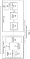
- MC 100 includes a traffic idle timer 110 that times an idle period from when the last access (read or write operation) was performed on DRAM 105. Should the idle period not exceed an idle threshold, MC 100 continues to operate in a refresh mode of operation in which MC 100 controls the scheduling of refresh cycles in DRAM 105. To do so, MC 100 includes a refresh timer 115 that times a delay from the last memory-controller-triggered refresh cycle for DRAM 105.
- refresh timer 115 asserts a refresh command (cmd) 120 to a command scheduler 125.
- command scheduler 125 commands a command decoder 130 in DRAM 105 to trigger a refresh circuit 135 to perform a refresh cycle.
- refresh timer 115 periodically triggers a refresh cycle in DRAM 105 at a rate determined by the refresh interval during the refresh mode of operation.
- traffic idle timer 110 may assert a self-refresh command (cmd) 150 to command scheduler 125.
- command scheduler 125 commands command decoder 130 to command DRAM 105 to enter the self-refresh mode of operation.
- traffic idle timer 110 asserts self-refresh command 150, it also triggers refresh timer 115 to write to a mode register 140 in DRAM 105 so as to inform DRAM 105 of when the last memory-controller-triggered refresh cycle occurred. This communication may be performed by refresh timer 115 writing into mode register 140 the time expired since the last (most-recent) memory-controller-triggered refresh cycle or the time remaining in the current refresh interval.
- refresh timer 115 may digitize the remaining portion (if any) of the current refresh interval since the most-recent-memory-controller-triggered refresh cycle. For example, refresh timer 115 may use a three-bit digitization such that it may estimate in increments of 1/8 the remaining portion of the current refresh interval. Alternatively, refresh timer 115 may use a four-bit digitization (increments of 1/16) or lower or higher orders of digitization. The following discussion will assume without loss of generality that refresh timer 115 writes a digitized remaining portion of the current refresh interval into mode register 140 as this requires relatively few bits and is thus bandwidth efficient.
- DRAM 105 may then enter the self-refresh mode of operation by loading the digitized estimated remaining portion of the current refresh interval from mode register 140 into a self-refresh timer 145. For example, if refresh timer 115 had indicated that there was 1/8 th remaining of the current refresh interval, self-refresh timer 145 may then count down to just 1/8 th of the refresh interval before triggering the initial DRAM-triggered self-refresh cycle in DRAM refresh circuit 135. After triggering this initial self-refresh cycle, self-refresh timer 145 would then count down from the full refresh interval for the triggering of subsequent self-refresh cycles. DRAM 105 would then manage its self-refresh cycles until SoC memory controller 100 resumes normal operation and exits the sleep mode.
- the refresh timer 115 may also inform DRAM 105 of the current temperature multiplier for the refresh interval.
- the leakage from the capacitors in the DRAM memory cells increases with temperature. Therefore it may be advantageous to decrease the refresh interval with increasing temperature, whether in a memory controller-triggered refresh cycle or in a self-refresh cycle controlled by the DRAM.
- this decrease in the refresh interval may also be digitized using a certain number of bits and represented by a digitized temperature multiplier. For example, suppose that the temperature multiplier is digitized into a 3-bit number. At room temperature the digitized temperature multiplier may equal one in that no reduction in the refresh interval is indicated. As the temperature increases, the digitized temperature multiplier may progressively decrease from one.
- Refresh timer 115 may thus also write the digitized temperature multiplier into mode register 140 or another register (not illustrated) in DRAM 105 analogous to the write by memory controller 100 of the remaining portion of the refresh cycle to mode register 140.
- self-refresh timer 145 may write a digitized remaining portion (if any) of the current refresh interval into mode register 140 (or another suitable register) as shown in Figure 2 .
- Refresh timer 115 may then read the contents of mode register 140 so that it counts down from the remaining portion of the refresh interval for the initial refresh cycle upon transition into the refresh mode. After refresh timer 115 triggers the initial refresh cycle according to whatever portion remains as notified through the read from mode register 140, refresh timer 115 would then count down using the entire refresh interval for any subsequent memory-controller-triggered refresh cycles until another transition to the self-refresh mode of operation.
- self-refresh timer 145 may also write a current digitized temperature multiplier into mode register 140 or another analogous register. Refresh timer 115 would then use this multiplier in conjunction with the remaining refresh interval portion from mode register 140. For example, suppose that mode register 140 indicates that the last DRAM-triggered refresh cycle took place 1 ⁇ 2 of the refresh interval ago. If DRAM 105 indicates that the temperature multiplier is 1 ⁇ 2 due to an elevated DRAM temperature, refresh timer 115 would then count down not from 1 ⁇ 2 of the default (room temperature) refresh interval but from 1 ⁇ 4 of the default refresh interval due to the reduction from the elevated temperature.
- Figure 3A is a flowchart for a refresh-mode to a self-refresh mode of operation such as discussed with regard to Figure 1 .
- the method includes an act 300 of transitioning a memory controller from an active mode of operation to a sleep mode of operation while the memory controller still has a portion remaining in a current refresh cycle for a DRAM.
- the transition of memory controller 100 of Figure 2 from the active mode to a sleep mode of operation is an example of act 300.
- the method further includes an act 305 of, from the memory controller, communicating the portion remaining in the current refresh cycle to the DRAM prior to the transition into the sleep mode of operation.
- the writing into mode register 140 by refresh timer 115 identifying the portion remaining of the current refresh cycle is an example of act 305.
- the method includes an act 310 of triggering a self-refresh cycle in the DRAM responsive to a countdown in the DRAM of the portion remaining in the current refresh cycle.
- the countdown in self-refresh timer 145 and subsequent triggering of a self-refresh cycle by refresh circuit 135 is an example of act 310.
- Figure 3B is a flowchart showing a method for entering a self-refresh mode of operation from a refresh mode of operation.
- the method includes an act 315 transitioning a memory controller from a sleep mode of operation to an active mode of operation.
- the transition of memory controller 100 in Figure 2 from the sleep mode of operation to the active mode of operation is an example of act 315.
- the method also includes an act 320 of receiving at the memory controller an indication from a dynamic random access memory (DRAM) of a remaining portion of a self-refresh interval since a most-recent DRAM-triggered self-refresh of the DRAM.
- DRAM dynamic random access memory
- the reading of mode register 140 by refresh timer 115 is an example of act 320.
- the method includes an act 325 of, in the memory controller, counting down the remaining portion of the self-refresh interval.
- the counting down of the remaining portion by refresh timer 115 of the self-refresh interval as retrieved from mode register 140 is an example of act 325.
- the method includes an act 330 of, from the memory controller, triggering a refresh cycle in the DRAM responsive to the counting down of the remaining portion of the self-refresh interval.
- the triggering by command scheduler 125 of a refresh cycle in DRAM 105 is an example of act 330.
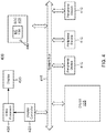
- the memory controller 100 may be incorporated within a system-on-a-chip (SoC) 405 within a device 400 as shown in Figure 4 .
- Device 400 may comprise a cellular phone, smart phone, personal digital assistant, tablet computer, laptop computer, digital camera, handheld gaming device, or other suitable device.
- Memory controller 100 within SoC 405 communicates with DRAM 105 over a system bus 415.
- SoC also communicates with peripheral devices 410 such as sensors over system bus 415.
- a display controller 425 also couples to system bus 415. In turn display controller 425 couples to a video processor 430 that drives a display 435.
- SoC 405 may also include a temperature sensor 440 in or near the DRAM 105 to monitor the temperature of DRAM 105.
- the steps of a method or algorithm described in connection with the disclosure may be embodied directly in hardware, in a software module executed by a processor, or in a combination of the two. If implemented in software, the functions may be stored on one or more instructions or code on a computer-readable medium.
- An exemplary computer-readable medium is coupled to the processor such that the processor can read information from, and write information to, the computer-readable medium. In the alternative, the computer-readable medium may be integral to the processor.
Landscapes
- Engineering & Computer Science (AREA)
- Microelectronics & Electronic Packaging (AREA)
- Computer Hardware Design (AREA)
- Theoretical Computer Science (AREA)
- Physics & Mathematics (AREA)
- General Engineering & Computer Science (AREA)
- General Physics & Mathematics (AREA)
- Dram (AREA)
Applications Claiming Priority (3)
| Application Number | Priority Date | Filing Date | Title |
|---|---|---|---|
| US201562236008P | 2015-10-01 | 2015-10-01 | |
| US15/246,371 US9875785B2 (en) | 2015-10-01 | 2016-08-24 | Refresh timer synchronization between memory controller and memory |
| PCT/US2016/048771 WO2017058417A1 (en) | 2015-10-01 | 2016-08-25 | Refresh timer synchronization between memory controller and memory |
Publications (2)
| Publication Number | Publication Date |
|---|---|
| EP3357065A1 EP3357065A1 (en) | 2018-08-08 |
| EP3357065B1 true EP3357065B1 (en) | 2019-06-26 |
Family
ID=56852438
Family Applications (1)
| Application Number | Title | Priority Date | Filing Date |
|---|---|---|---|
| EP16759956.2A Active EP3357065B1 (en) | 2015-10-01 | 2016-08-25 | Refresh timer synchronization between memory controller and memory |
Country Status (7)
Families Citing this family (11)
| Publication number | Priority date | Publication date | Assignee | Title |
|---|---|---|---|---|
| US20180061484A1 (en) * | 2016-08-29 | 2018-03-01 | Apple Inc. | Systems and Methods for Memory Refresh Timing |
| US20190074051A1 (en) * | 2017-09-07 | 2019-03-07 | Mediatek Inc. | Memory system and refresh control method thereof |
| US10552087B2 (en) | 2018-06-04 | 2020-02-04 | Micron Technology, Inc. | Methods for performing multiple memory operations in response to a single command and memory devices and systems employing the same |
| KR102578002B1 (ko) * | 2018-07-03 | 2023-09-14 | 에스케이하이닉스 주식회사 | 메모리 시스템 및 이의 동작 방법 |
| US10685722B1 (en) * | 2019-01-24 | 2020-06-16 | Western Digital Technologies, Inc. | Method and system for improving performance of a storage device using asynchronous independent plane read functionality |
| US11250902B2 (en) * | 2019-09-26 | 2022-02-15 | Intel Corporation | Method and apparatus to reduce power consumption for refresh of memory devices on a memory module |
| KR102839272B1 (ko) * | 2020-07-02 | 2025-07-29 | 에스케이하이닉스 주식회사 | 저장 장치 및 그 동작 방법 |
| KR102786984B1 (ko) | 2020-09-03 | 2025-03-27 | 삼성전자주식회사 | 메모리 장치, 그것을 포함하는 메모리 시스템, 그것을 제어하는 제어기 및 그것의 동작 방법 |
| KR20220091162A (ko) | 2020-12-23 | 2022-06-30 | 삼성전자주식회사 | 온도에 대한 리프레쉬 레이트 승수와 상관없는 메모리 장치의 리프레쉬 방법 |
| TWI740773B (zh) * | 2021-01-27 | 2021-09-21 | 華邦電子股份有限公司 | 半導體記憶裝置 |
| US12142312B2 (en) * | 2022-09-13 | 2024-11-12 | Nanya Technology Corporation | Memory control circuit and refresh method for dynamic random access memory array |
Family Cites Families (30)
| Publication number | Priority date | Publication date | Assignee | Title |
|---|---|---|---|---|
| JPH07182857A (ja) * | 1993-12-24 | 1995-07-21 | Toshiba Corp | マイコンシステム |
| JPH09213071A (ja) * | 1996-02-02 | 1997-08-15 | Hitachi Ltd | 半導体記憶装置 |
| US5808952A (en) * | 1996-10-28 | 1998-09-15 | Silicon Magic Corporation | Adaptive auto refresh |
| US6212599B1 (en) * | 1997-11-26 | 2001-04-03 | Intel Corporation | Method and apparatus for a memory control system including a secondary controller for DRAM refresh during sleep mode |
| US6118719A (en) * | 1998-05-20 | 2000-09-12 | International Business Machines Corporation | Self-initiated self-refresh mode for memory modules |
| CN1184644C (zh) * | 2001-03-16 | 2005-01-12 | 矽统科技股份有限公司 | 存储器刷新系统 |
| US6693837B2 (en) * | 2002-04-23 | 2004-02-17 | Micron Technology, Inc. | System and method for quick self-refresh exit with transitional refresh |
| JP4246971B2 (ja) * | 2002-07-15 | 2009-04-02 | 富士通マイクロエレクトロニクス株式会社 | 半導体メモリ |
| KR100529033B1 (ko) * | 2003-05-23 | 2005-11-17 | 주식회사 하이닉스반도체 | 동기식 반도체 메모리 소자 |
| US7236416B2 (en) * | 2004-05-21 | 2007-06-26 | Qualcomm Incorporated | Method and system for controlling refresh in volatile memories |
| US7088633B2 (en) | 2004-05-27 | 2006-08-08 | Qualcomm Incorporated | Method and system for providing seamless self-refresh for directed bank refresh in volatile memories |
| US7206244B2 (en) * | 2004-12-01 | 2007-04-17 | Freescale Semiconductor, Inc. | Temperature based DRAM refresh |
| KR100655076B1 (ko) * | 2005-01-20 | 2006-12-08 | 삼성전자주식회사 | 반도체 메모리 장치의 내부 온도 데이터 출력 방법 및그에 따른 내부 온도 데이터 출력회로 |
| US9384818B2 (en) | 2005-04-21 | 2016-07-05 | Violin Memory | Memory power management |
| JP4516483B2 (ja) * | 2005-06-07 | 2010-08-04 | 富士通セミコンダクター株式会社 | 半導体記憶装置及び情報処理システム |
| US7313047B2 (en) * | 2006-02-23 | 2007-12-25 | Hynix Semiconductor Inc. | Dynamic semiconductor memory with improved refresh mechanism |
| CN101000798B (zh) * | 2007-01-12 | 2010-05-19 | 威盛电子股份有限公司 | 存储器刷新方法及存储器刷新系统 |
| US8392650B2 (en) * | 2010-04-01 | 2013-03-05 | Intel Corporation | Fast exit from self-refresh state of a memory device |
| US9292426B2 (en) * | 2010-09-24 | 2016-03-22 | Intel Corporation | Fast exit from DRAM self-refresh |
| US9053812B2 (en) * | 2010-09-24 | 2015-06-09 | Intel Corporation | Fast exit from DRAM self-refresh |
| US10157657B2 (en) * | 2012-08-28 | 2018-12-18 | Rambus Inc. | Selective refresh with software components |
| KR20140076735A (ko) * | 2012-12-13 | 2014-06-23 | 삼성전자주식회사 | 휘발성 메모리 장치 및 메모리 시스템 |
| US9704557B2 (en) * | 2013-09-25 | 2017-07-11 | Qualcomm Incorporated | Method and apparatus for storing retention time profile information based on retention time and temperature |
| US9001608B1 (en) * | 2013-12-06 | 2015-04-07 | Intel Corporation | Coordinating power mode switching and refresh operations in a memory device |
| KR20160122586A (ko) * | 2015-04-14 | 2016-10-24 | 에스케이하이닉스 주식회사 | 반도체장치 및 이를 포함하는 반도체시스템 |
| KR102326018B1 (ko) * | 2015-08-24 | 2021-11-12 | 삼성전자주식회사 | 메모리 시스템 |
| KR102354987B1 (ko) * | 2015-10-22 | 2022-01-24 | 삼성전자주식회사 | 온도에 따라 셀프 리프레쉬 사이클을 제어하는 리프레쉬 방법 |
| KR102393426B1 (ko) * | 2015-11-10 | 2022-05-04 | 에스케이하이닉스 주식회사 | 반도체장치 |
| US9721640B2 (en) * | 2015-12-09 | 2017-08-01 | Intel Corporation | Performance of additional refresh operations during self-refresh mode |
| KR102419535B1 (ko) * | 2016-03-18 | 2022-07-13 | 에스케이하이닉스 주식회사 | 메모리 장치 |
-
2016
- 2016-08-24 US US15/246,371 patent/US9875785B2/en active Active
- 2016-08-25 WO PCT/US2016/048771 patent/WO2017058417A1/en active Application Filing
- 2016-08-25 JP JP2018516132A patent/JP2018530098A/ja active Pending
- 2016-08-25 KR KR1020187012415A patent/KR102593418B1/ko active Active
- 2016-08-25 CN CN201680058030.5A patent/CN108140406B/zh active Active
- 2016-08-25 EP EP16759956.2A patent/EP3357065B1/en active Active
- 2016-08-25 BR BR112018006477-7A patent/BR112018006477B1/pt active IP Right Grant
Non-Patent Citations (1)
| Title |
|---|
| None * |
Also Published As
| Publication number | Publication date |
|---|---|
| US9875785B2 (en) | 2018-01-23 |
| BR112018006477A2 (pt) | 2018-10-09 |
| WO2017058417A1 (en) | 2017-04-06 |
| JP2018530098A (ja) | 2018-10-11 |
| BR112018006477B1 (pt) | 2023-03-14 |
| CN108140406B (zh) | 2022-03-22 |
| CN108140406A (zh) | 2018-06-08 |
| KR102593418B1 (ko) | 2023-10-23 |
| EP3357065A1 (en) | 2018-08-08 |
| KR20180063230A (ko) | 2018-06-11 |
| US20170098470A1 (en) | 2017-04-06 |
Similar Documents
| Publication | Publication Date | Title |
|---|---|---|
| EP3357065B1 (en) | Refresh timer synchronization between memory controller and memory | |
| US9001608B1 (en) | Coordinating power mode switching and refresh operations in a memory device | |
| JP4922306B2 (ja) | C0時のセルフリフレッシュメカニズム | |
| US20130166932A1 (en) | Systems and methods of exiting hibernation in response to a triggering event | |
| US9104413B2 (en) | System and method for dynamic memory power management | |
| US10331195B2 (en) | Power and performance aware memory-controller voting mechanism | |
| CN109151961B (zh) | 一种移动终端的运行方法、终端及计算机可读存储介质 | |
| US20130232364A1 (en) | Hardware Automatic Performance State Transitions in System on Processor Sleep and Wake Events | |
| US10175995B1 (en) | Device hibernation control | |
| US10268486B1 (en) | Expedited resume process from hibernation | |
| US8190788B2 (en) | Shifting volatile memories to self-refresh mode | |
| EP3172635B1 (en) | Ultra low power architecture to support always on path to memory | |
| US10976800B2 (en) | Electronic device capable of reducing power consumption and method for reducing power consumption of electronic device | |
| TW201510999A (zh) | 用於動態隨機存取記憶體之智慧型更新的方法與系統 | |
| US10705590B2 (en) | Power-conserving cache memory usage | |
| CN105474182B (zh) | 在电子设备处于低功率模式的同时支持周期性写操作的存储设备 | |
| US20160320826A1 (en) | Methods and apparatuses for memory power reduction | |
| US10235309B1 (en) | Combined control for multi-die flash | |
| US10203749B2 (en) | Method and apparatus for saving power, including at least two power saving modes | |
| JP6054203B2 (ja) | 情報処理装置、デバイス制御方法及びプログラム | |
| US20150162069A1 (en) | Information processing terminal and power control method | |
| JPH046940A (ja) | ファクシミリ装置 |
Legal Events
| Date | Code | Title | Description |
|---|---|---|---|
| STAA | Information on the status of an ep patent application or granted ep patent |
Free format text: STATUS: THE INTERNATIONAL PUBLICATION HAS BEEN MADE |
|
| PUAI | Public reference made under article 153(3) epc to a published international application that has entered the european phase |
Free format text: ORIGINAL CODE: 0009012 |
|
| STAA | Information on the status of an ep patent application or granted ep patent |
Free format text: STATUS: REQUEST FOR EXAMINATION WAS MADE |
|
| 17P | Request for examination filed |
Effective date: 20180322 |
|
| AK | Designated contracting states |
Kind code of ref document: A1 Designated state(s): AL AT BE BG CH CY CZ DE DK EE ES FI FR GB GR HR HU IE IS IT LI LT LU LV MC MK MT NL NO PL PT RO RS SE SI SK SM TR |
|
| AX | Request for extension of the european patent |
Extension state: BA ME |
|
| DAV | Request for validation of the european patent (deleted) | ||
| DAX | Request for extension of the european patent (deleted) | ||
| GRAP | Despatch of communication of intention to grant a patent |
Free format text: ORIGINAL CODE: EPIDOSNIGR1 |
|
| STAA | Information on the status of an ep patent application or granted ep patent |
Free format text: STATUS: GRANT OF PATENT IS INTENDED |
|
| INTG | Intention to grant announced |
Effective date: 20190205 |
|
| GRAS | Grant fee paid |
Free format text: ORIGINAL CODE: EPIDOSNIGR3 |
|
| GRAA | (expected) grant |
Free format text: ORIGINAL CODE: 0009210 |
|
| STAA | Information on the status of an ep patent application or granted ep patent |
Free format text: STATUS: THE PATENT HAS BEEN GRANTED |
|
| AK | Designated contracting states |
Kind code of ref document: B1 Designated state(s): AL AT BE BG CH CY CZ DE DK EE ES FI FR GB GR HR HU IE IS IT LI LT LU LV MC MK MT NL NO PL PT RO RS SE SI SK SM TR |
|
| REG | Reference to a national code |
Ref country code: GB Ref legal event code: FG4D |
|
| REG | Reference to a national code |
Ref country code: CH Ref legal event code: EP |
|
| REG | Reference to a national code |
Ref country code: AT Ref legal event code: REF Ref document number: 1149243 Country of ref document: AT Kind code of ref document: T Effective date: 20190715 |
|
| REG | Reference to a national code |
Ref country code: IE Ref legal event code: FG4D |
|
| REG | Reference to a national code |
Ref country code: DE Ref legal event code: R096 Ref document number: 602016016006 Country of ref document: DE |
|
| REG | Reference to a national code |
Ref country code: NL Ref legal event code: MP Effective date: 20190626 |
|
| PG25 | Lapsed in a contracting state [announced via postgrant information from national office to epo] |
Ref country code: SE Free format text: LAPSE BECAUSE OF FAILURE TO SUBMIT A TRANSLATION OF THE DESCRIPTION OR TO PAY THE FEE WITHIN THE PRESCRIBED TIME-LIMIT Effective date: 20190626 Ref country code: HR Free format text: LAPSE BECAUSE OF FAILURE TO SUBMIT A TRANSLATION OF THE DESCRIPTION OR TO PAY THE FEE WITHIN THE PRESCRIBED TIME-LIMIT Effective date: 20190626 Ref country code: NO Free format text: LAPSE BECAUSE OF FAILURE TO SUBMIT A TRANSLATION OF THE DESCRIPTION OR TO PAY THE FEE WITHIN THE PRESCRIBED TIME-LIMIT Effective date: 20190926 Ref country code: AL Free format text: LAPSE BECAUSE OF FAILURE TO SUBMIT A TRANSLATION OF THE DESCRIPTION OR TO PAY THE FEE WITHIN THE PRESCRIBED TIME-LIMIT Effective date: 20190626 Ref country code: FI Free format text: LAPSE BECAUSE OF FAILURE TO SUBMIT A TRANSLATION OF THE DESCRIPTION OR TO PAY THE FEE WITHIN THE PRESCRIBED TIME-LIMIT Effective date: 20190626 Ref country code: LT Free format text: LAPSE BECAUSE OF FAILURE TO SUBMIT A TRANSLATION OF THE DESCRIPTION OR TO PAY THE FEE WITHIN THE PRESCRIBED TIME-LIMIT Effective date: 20190626 |
|
| REG | Reference to a national code |
Ref country code: LT Ref legal event code: MG4D |
|
| PG25 | Lapsed in a contracting state [announced via postgrant information from national office to epo] |
Ref country code: GR Free format text: LAPSE BECAUSE OF FAILURE TO SUBMIT A TRANSLATION OF THE DESCRIPTION OR TO PAY THE FEE WITHIN THE PRESCRIBED TIME-LIMIT Effective date: 20190927 Ref country code: BG Free format text: LAPSE BECAUSE OF FAILURE TO SUBMIT A TRANSLATION OF THE DESCRIPTION OR TO PAY THE FEE WITHIN THE PRESCRIBED TIME-LIMIT Effective date: 20190926 Ref country code: RS Free format text: LAPSE BECAUSE OF FAILURE TO SUBMIT A TRANSLATION OF THE DESCRIPTION OR TO PAY THE FEE WITHIN THE PRESCRIBED TIME-LIMIT Effective date: 20190626 Ref country code: LV Free format text: LAPSE BECAUSE OF FAILURE TO SUBMIT A TRANSLATION OF THE DESCRIPTION OR TO PAY THE FEE WITHIN THE PRESCRIBED TIME-LIMIT Effective date: 20190626 |
|
| REG | Reference to a national code |
Ref country code: AT Ref legal event code: MK05 Ref document number: 1149243 Country of ref document: AT Kind code of ref document: T Effective date: 20190626 |
|
| PG25 | Lapsed in a contracting state [announced via postgrant information from national office to epo] |
Ref country code: NL Free format text: LAPSE BECAUSE OF FAILURE TO SUBMIT A TRANSLATION OF THE DESCRIPTION OR TO PAY THE FEE WITHIN THE PRESCRIBED TIME-LIMIT Effective date: 20190626 Ref country code: EE Free format text: LAPSE BECAUSE OF FAILURE TO SUBMIT A TRANSLATION OF THE DESCRIPTION OR TO PAY THE FEE WITHIN THE PRESCRIBED TIME-LIMIT Effective date: 20190626 Ref country code: AT Free format text: LAPSE BECAUSE OF FAILURE TO SUBMIT A TRANSLATION OF THE DESCRIPTION OR TO PAY THE FEE WITHIN THE PRESCRIBED TIME-LIMIT Effective date: 20190626 Ref country code: RO Free format text: LAPSE BECAUSE OF FAILURE TO SUBMIT A TRANSLATION OF THE DESCRIPTION OR TO PAY THE FEE WITHIN THE PRESCRIBED TIME-LIMIT Effective date: 20190626 Ref country code: CZ Free format text: LAPSE BECAUSE OF FAILURE TO SUBMIT A TRANSLATION OF THE DESCRIPTION OR TO PAY THE FEE WITHIN THE PRESCRIBED TIME-LIMIT Effective date: 20190626 Ref country code: SK Free format text: LAPSE BECAUSE OF FAILURE TO SUBMIT A TRANSLATION OF THE DESCRIPTION OR TO PAY THE FEE WITHIN THE PRESCRIBED TIME-LIMIT Effective date: 20190626 Ref country code: PT Free format text: LAPSE BECAUSE OF FAILURE TO SUBMIT A TRANSLATION OF THE DESCRIPTION OR TO PAY THE FEE WITHIN THE PRESCRIBED TIME-LIMIT Effective date: 20191028 |
|
| PG25 | Lapsed in a contracting state [announced via postgrant information from national office to epo] |
Ref country code: IS Free format text: LAPSE BECAUSE OF FAILURE TO SUBMIT A TRANSLATION OF THE DESCRIPTION OR TO PAY THE FEE WITHIN THE PRESCRIBED TIME-LIMIT Effective date: 20191026 Ref country code: SM Free format text: LAPSE BECAUSE OF FAILURE TO SUBMIT A TRANSLATION OF THE DESCRIPTION OR TO PAY THE FEE WITHIN THE PRESCRIBED TIME-LIMIT Effective date: 20190626 Ref country code: IT Free format text: LAPSE BECAUSE OF FAILURE TO SUBMIT A TRANSLATION OF THE DESCRIPTION OR TO PAY THE FEE WITHIN THE PRESCRIBED TIME-LIMIT Effective date: 20190626 Ref country code: ES Free format text: LAPSE BECAUSE OF FAILURE TO SUBMIT A TRANSLATION OF THE DESCRIPTION OR TO PAY THE FEE WITHIN THE PRESCRIBED TIME-LIMIT Effective date: 20190626 |
|
| PG25 | Lapsed in a contracting state [announced via postgrant information from national office to epo] |
Ref country code: TR Free format text: LAPSE BECAUSE OF FAILURE TO SUBMIT A TRANSLATION OF THE DESCRIPTION OR TO PAY THE FEE WITHIN THE PRESCRIBED TIME-LIMIT Effective date: 20190626 |
|
| PG25 | Lapsed in a contracting state [announced via postgrant information from national office to epo] |
Ref country code: DK Free format text: LAPSE BECAUSE OF FAILURE TO SUBMIT A TRANSLATION OF THE DESCRIPTION OR TO PAY THE FEE WITHIN THE PRESCRIBED TIME-LIMIT Effective date: 20190626 Ref country code: PL Free format text: LAPSE BECAUSE OF FAILURE TO SUBMIT A TRANSLATION OF THE DESCRIPTION OR TO PAY THE FEE WITHIN THE PRESCRIBED TIME-LIMIT Effective date: 20190626 |
|
| PG25 | Lapsed in a contracting state [announced via postgrant information from national office to epo] |
Ref country code: IS Free format text: LAPSE BECAUSE OF FAILURE TO SUBMIT A TRANSLATION OF THE DESCRIPTION OR TO PAY THE FEE WITHIN THE PRESCRIBED TIME-LIMIT Effective date: 20200224 Ref country code: LU Free format text: LAPSE BECAUSE OF NON-PAYMENT OF DUE FEES Effective date: 20190825 Ref country code: LI Free format text: LAPSE BECAUSE OF NON-PAYMENT OF DUE FEES Effective date: 20190831 Ref country code: CH Free format text: LAPSE BECAUSE OF NON-PAYMENT OF DUE FEES Effective date: 20190831 Ref country code: MC Free format text: LAPSE BECAUSE OF FAILURE TO SUBMIT A TRANSLATION OF THE DESCRIPTION OR TO PAY THE FEE WITHIN THE PRESCRIBED TIME-LIMIT Effective date: 20190626 |
|
| REG | Reference to a national code |
Ref country code: BE Ref legal event code: MM Effective date: 20190831 |
|
| REG | Reference to a national code |
Ref country code: DE Ref legal event code: R097 Ref document number: 602016016006 Country of ref document: DE |
|
| PLBE | No opposition filed within time limit |
Free format text: ORIGINAL CODE: 0009261 |
|
| STAA | Information on the status of an ep patent application or granted ep patent |
Free format text: STATUS: NO OPPOSITION FILED WITHIN TIME LIMIT |
|
| PG2D | Information on lapse in contracting state deleted |
Ref country code: IS |
|
| PG25 | Lapsed in a contracting state [announced via postgrant information from national office to epo] |
Ref country code: IE Free format text: LAPSE BECAUSE OF NON-PAYMENT OF DUE FEES Effective date: 20190825 |
|
| 26N | No opposition filed |
Effective date: 20200603 |
|
| PG25 | Lapsed in a contracting state [announced via postgrant information from national office to epo] |
Ref country code: BE Free format text: LAPSE BECAUSE OF NON-PAYMENT OF DUE FEES Effective date: 20190831 Ref country code: SI Free format text: LAPSE BECAUSE OF FAILURE TO SUBMIT A TRANSLATION OF THE DESCRIPTION OR TO PAY THE FEE WITHIN THE PRESCRIBED TIME-LIMIT Effective date: 20190626 |
|
| PG25 | Lapsed in a contracting state [announced via postgrant information from national office to epo] |
Ref country code: CY Free format text: LAPSE BECAUSE OF FAILURE TO SUBMIT A TRANSLATION OF THE DESCRIPTION OR TO PAY THE FEE WITHIN THE PRESCRIBED TIME-LIMIT Effective date: 20190626 |
|
| PG25 | Lapsed in a contracting state [announced via postgrant information from national office to epo] |
Ref country code: MT Free format text: LAPSE BECAUSE OF FAILURE TO SUBMIT A TRANSLATION OF THE DESCRIPTION OR TO PAY THE FEE WITHIN THE PRESCRIBED TIME-LIMIT Effective date: 20190626 Ref country code: HU Free format text: LAPSE BECAUSE OF FAILURE TO SUBMIT A TRANSLATION OF THE DESCRIPTION OR TO PAY THE FEE WITHIN THE PRESCRIBED TIME-LIMIT; INVALID AB INITIO Effective date: 20160825 |
|
| PG25 | Lapsed in a contracting state [announced via postgrant information from national office to epo] |
Ref country code: MK Free format text: LAPSE BECAUSE OF FAILURE TO SUBMIT A TRANSLATION OF THE DESCRIPTION OR TO PAY THE FEE WITHIN THE PRESCRIBED TIME-LIMIT Effective date: 20190626 |
|
| PGFP | Annual fee paid to national office [announced via postgrant information from national office to epo] |
Ref country code: DE Payment date: 20240709 Year of fee payment: 9 |
|
| PGFP | Annual fee paid to national office [announced via postgrant information from national office to epo] |
Ref country code: GB Payment date: 20240711 Year of fee payment: 9 |
|
| PGFP | Annual fee paid to national office [announced via postgrant information from national office to epo] |
Ref country code: FR Payment date: 20240710 Year of fee payment: 9 |