EP3355295A1 - Unité de goa, circuit de pilotage de grille et dispositif d'affichage - Google Patents
Unité de goa, circuit de pilotage de grille et dispositif d'affichage Download PDFInfo
- Publication number
- EP3355295A1 EP3355295A1 EP16822364.2A EP16822364A EP3355295A1 EP 3355295 A1 EP3355295 A1 EP 3355295A1 EP 16822364 A EP16822364 A EP 16822364A EP 3355295 A1 EP3355295 A1 EP 3355295A1
- Authority
- EP
- European Patent Office
- Prior art keywords
- circuit
- transistor
- sub
- goa unit
- low
- Prior art date
- Legal status (The legal status is an assumption and is not a legal conclusion. Google has not performed a legal analysis and makes no representation as to the accuracy of the status listed.)
- Withdrawn
Links
Images


Classifications
-
- G—PHYSICS
- G09—EDUCATION; CRYPTOGRAPHY; DISPLAY; ADVERTISING; SEALS
- G09G—ARRANGEMENTS OR CIRCUITS FOR CONTROL OF INDICATING DEVICES USING STATIC MEANS TO PRESENT VARIABLE INFORMATION
- G09G3/00—Control arrangements or circuits, of interest only in connection with visual indicators other than cathode-ray tubes
- G09G3/20—Control arrangements or circuits, of interest only in connection with visual indicators other than cathode-ray tubes for presentation of an assembly of a number of characters, e.g. a page, by composing the assembly by combination of individual elements arranged in a matrix no fixed position being assigned to or needed to be assigned to the individual characters or partial characters
- G09G3/2092—Details of a display terminals using a flat panel, the details relating to the control arrangement of the display terminal and to the interfaces thereto
-
- G—PHYSICS
- G09—EDUCATION; CRYPTOGRAPHY; DISPLAY; ADVERTISING; SEALS
- G09G—ARRANGEMENTS OR CIRCUITS FOR CONTROL OF INDICATING DEVICES USING STATIC MEANS TO PRESENT VARIABLE INFORMATION
- G09G3/00—Control arrangements or circuits, of interest only in connection with visual indicators other than cathode-ray tubes
- G09G3/20—Control arrangements or circuits, of interest only in connection with visual indicators other than cathode-ray tubes for presentation of an assembly of a number of characters, e.g. a page, by composing the assembly by combination of individual elements arranged in a matrix no fixed position being assigned to or needed to be assigned to the individual characters or partial characters
-
- G—PHYSICS
- G11—INFORMATION STORAGE
- G11C—STATIC STORES
- G11C19/00—Digital stores in which the information is moved stepwise, e.g. shift registers
- G11C19/18—Digital stores in which the information is moved stepwise, e.g. shift registers using capacitors as main elements of the stages
- G11C19/182—Digital stores in which the information is moved stepwise, e.g. shift registers using capacitors as main elements of the stages in combination with semiconductor elements, e.g. bipolar transistors, diodes
- G11C19/184—Digital stores in which the information is moved stepwise, e.g. shift registers using capacitors as main elements of the stages in combination with semiconductor elements, e.g. bipolar transistors, diodes with field-effect transistors, e.g. MOS-FET
-
- G—PHYSICS
- G09—EDUCATION; CRYPTOGRAPHY; DISPLAY; ADVERTISING; SEALS
- G09G—ARRANGEMENTS OR CIRCUITS FOR CONTROL OF INDICATING DEVICES USING STATIC MEANS TO PRESENT VARIABLE INFORMATION
- G09G2300/00—Aspects of the constitution of display devices
- G09G2300/08—Active matrix structure, i.e. with use of active elements, inclusive of non-linear two terminal elements, in the pixels together with light emitting or modulating elements
- G09G2300/0809—Several active elements per pixel in active matrix panels
- G09G2300/0819—Several active elements per pixel in active matrix panels used for counteracting undesired variations, e.g. feedback or autozeroing
-
- G—PHYSICS
- G09—EDUCATION; CRYPTOGRAPHY; DISPLAY; ADVERTISING; SEALS
- G09G—ARRANGEMENTS OR CIRCUITS FOR CONTROL OF INDICATING DEVICES USING STATIC MEANS TO PRESENT VARIABLE INFORMATION
- G09G2310/00—Command of the display device
- G09G2310/02—Addressing, scanning or driving the display screen or processing steps related thereto
- G09G2310/0264—Details of driving circuits
- G09G2310/0267—Details of drivers for scan electrodes, other than drivers for liquid crystal, plasma or OLED displays
-
- G—PHYSICS
- G09—EDUCATION; CRYPTOGRAPHY; DISPLAY; ADVERTISING; SEALS
- G09G—ARRANGEMENTS OR CIRCUITS FOR CONTROL OF INDICATING DEVICES USING STATIC MEANS TO PRESENT VARIABLE INFORMATION
- G09G2310/00—Command of the display device
- G09G2310/02—Addressing, scanning or driving the display screen or processing steps related thereto
- G09G2310/0264—Details of driving circuits
- G09G2310/0286—Details of a shift registers arranged for use in a driving circuit
-
- G—PHYSICS
- G09—EDUCATION; CRYPTOGRAPHY; DISPLAY; ADVERTISING; SEALS
- G09G—ARRANGEMENTS OR CIRCUITS FOR CONTROL OF INDICATING DEVICES USING STATIC MEANS TO PRESENT VARIABLE INFORMATION
- G09G2310/00—Command of the display device
- G09G2310/08—Details of timing specific for flat panels, other than clock recovery
-
- G—PHYSICS
- G09—EDUCATION; CRYPTOGRAPHY; DISPLAY; ADVERTISING; SEALS
- G09G—ARRANGEMENTS OR CIRCUITS FOR CONTROL OF INDICATING DEVICES USING STATIC MEANS TO PRESENT VARIABLE INFORMATION
- G09G2320/00—Control of display operating conditions
- G09G2320/02—Improving the quality of display appearance
- G09G2320/0209—Crosstalk reduction, i.e. to reduce direct or indirect influences of signals directed to a certain pixel of the displayed image on other pixels of said image, inclusive of influences affecting pixels in different frames or fields or sub-images which constitute a same image, e.g. left and right images of a stereoscopic display
-
- G—PHYSICS
- G09—EDUCATION; CRYPTOGRAPHY; DISPLAY; ADVERTISING; SEALS
- G09G—ARRANGEMENTS OR CIRCUITS FOR CONTROL OF INDICATING DEVICES USING STATIC MEANS TO PRESENT VARIABLE INFORMATION
- G09G2330/00—Aspects of power supply; Aspects of display protection and defect management
- G09G2330/02—Details of power systems and of start or stop of display operation
Definitions
- the present disclosure relates to the field of display technology, in particular to a gate on array (GOA) unit, a gate driver circuit and a display device.
- GOA gate on array
- a gate driver circuit provides on signals, so that a plurality of rows of pixels can be sequentially and progressively switched on, and hence display can be achieved.
- the gate driver circuit includes multi-stage shift registers, and each shift register corresponds to one row of pixels. Before switching on a row of pixels, a shift register corresponding to the row of pixels generates a driving signal, which is hence inputted into a gate line connected with the row of pixels, thereby driving the row of pixels to be switched on.
- GOA Gate Driver circuit
- each GOA unit outputs an off signal after driving one row of pixels corresponding to the GOA unit to be switched on and is in a flooding state.
- the GOA unit in the flooding state can be easily and incorrectly switched on by a signal which is coupled in, causing one row of pixels that correspond to the GOA unit to be charged and switched on.
- incorrect images can be displayed, that is, an "abnormal image" phenomenon can be caused.
- Embodiments of the present disclosure provide a GOA unit, a gate driver circuit and a display device in order to solve at least the above technical problems in existing technologies, which can avoid the incorrect switching-on of one row of pixels corresponding to the GOA unit, so that the row of pixels cannot be charged and display incorrect images, and hence the "abnormal image" phenomenon can be overcome.
- Embodiments of the present disclosure provide a gate on array (GOA) unit, comprising: a driver circuit configured to output a first clock signal from an output end of the GOA unit; and a pull-down circuit connected with the driver circuit, the pull-down circuit also connected with at least one low-voltage end that provides a low-voltage signal, the pull-down circuit configured to input the low-voltage signal into a control end of the driver circuit to drive the driver circuit to be in an off state when the GOA unit outputs an off signal.
- GOA gate on array
- the pull-down circuit includes a first sub-circuit, a second sub-circuit and a third sub-circuit.
- a first end of the first sub-circuit is connected with the control end of the driver circuit; a second end of the first sub-circuit is connected with the at least one low-voltage end; a third end of the first sub-circuit is connected with the second sub-circuit and the third sub-circuit.
- a first end of the second sub-circuit is connected with a signal input end; a second end of the second sub-circuit is connected with a second clock signal; a third end of the second sub-circuit is connected with the third end of the first sub-circuit.
- a first end of the third sub-circuit is connected with the at least one low-voltage end; a second end of the third sub-circuit is connected with the control end of the driver circuit; and a third end of the third sub-circuit is connected with the third end of the first sub-circuit.
- the pull-down circuit further includes a fourth sub-circuit.
- a first end of the fourth sub-circuit is connected with the output end of the GOA unit; a second end of the fourth sub-circuit is connected with the at least one low-voltage end; and a third end of the fourth sub-circuit is connected with the third end of the second sub-circuit and the third end of the third sub-circuit.
- the second sub-circuit includes a first transistor and a second transistor.
- a control electrode of the first transistor is the second end of the second sub-circuit and connected with the second clock signal;
- a source electrode of the first transistor is the first end of the second sub-circuit and connected with the signal input end;
- a drain electrode of the first transistor is connected with a control electrode and a source electrode of the second transistor.
- a drain electrode of the second transistor is the third end of the second sub-circuit and connected with the third end of the first sub-circuit.
- a high voltage signal or the second clock signal is inputted from the signal input end.
- the third sub-circuit includes a third transistor.
- a control electrode of the third transistor is the second end of the third sub-circuit and connected with the control end of the driver circuit; a source electrode of the third transistor is the first end of the third sub-circuit and connected with the at least one low-voltage end; and a drain electrode of the third transistor is the third end of the third sub-circuit and connected with the third end of the first sub-circuit.
- the first sub-circuit includes a fourth transistor.
- a control electrode of the fourth transistor is the third end of the first sub-circuit and connected with the second sub-circuit and the third sub-circuit;
- a source electrode of the fourth transistor is the second end of the first sub-circuit and connected with the at least one low-voltage end;
- a drain electrode of the fourth transistor is the first end of the first sub-circuit and connected with the control end of the driver circuit.
- the fourth sub-circuit includes a fifth transistor.
- a control electrode of the fifth transistor is the third end of the fourth sub-circuit and connected with the third end of the second sub-circuit and the third end of the third sub-circuit;
- a source electrode of the fifth transistor is the second end of the fourth sub-circuit and connected with the at least one low-voltage end;
- a drain electrode of the fifth transistor is the first end of the fourth sub-circuit and connected with the output end of the GOA unit.
- the first sub-circuit includes a fourth transistor; the second sub-circuit includes a first transistor and a second transistor; the third sub-circuit includes a third transistor.
- a control electrode of the first transistor is connected with the second clock signal; a source electrode of the first transistor is connected with the signal input end; a drain electrode of the first transistor is connected with a control electrode and a source electrode of the second transistor.
- a drain electrode of the second transistor is connected with a control electrode of the fourth transistor.
- a control electrode of the third transistor is connected with the control end of the driver circuit; a source electrode of the third transistor is connected with the at least one low-voltage end; a drain electrode of the third transistor is connected with a control electrode of the fourth transistor.
- a source electrode of the fourth transistor is connected with the at least one low-voltage end; a drain electrode of the fourth transistor is connected with the control end of the driver circuit.
- a high voltage signal or the second clock signal is inputted from the signal input end.
- a low-voltage end connected with the source electrode of the third transistor and a low-voltage end connected with the source electrode of the fourth transistor are a same voltage end.
- the pull-down circuit further includes a fourth sub-circuit; the fourth sub-circuit includes a fifth transistor.
- a control electrode of the fifth transistor is connected with the control electrode of the fourth transistor; a source electrode of the fifth transistor is connected with the at least one low-voltage end; and a drain electrode of the fifth transistor is connected with the output end of the GOA unit.
- a low-voltage end connected with the source electrode of the third transistor, a low-voltage end connected with the source electrode of the fourth transistor, and a low-voltage end connected with the source electrode of the fifth transistor are a same voltage end.
- the GOA unit further includes a pull-up circuit.
- An output end of the pull-up circuit is connected with the driver circuit so as to input a pull-up signal into the driver circuit; and the pull-up signal is configured to drive the driver circuit to be switched on.
- the driver circuit includes a driving transistor.
- a control electrode of the driving transistor is the control end of the driver circuit and connected with the output end of the pull-up circuit; a source electrode of the driving transistor is connected with the first clock signal; and a drain electrode of the driving transistor is connected with the output end of the GOA unit.
- the GOA unit further includes a reset circuit.
- the reset circuit is connected with the driver circuit and configured to input the low-voltage signal into the control end of the driver circuit and the output end of the GOA unit; and the low-voltage signal is configured to drive the driver circuit to be switched off and pull down a signal outputted by the GOA unit.
- the pull-up circuit includes a sixth transistor and a first capacitor.
- a control electrode and a source electrode of the sixth transistor are connected with the pull-up signal; a drain electrode of the sixth transistor is connected with the control electrode of the driving transistor.
- a first end of the first capacitor is connected between the drain electrode of the sixth transistor and the control electrode of the driving transistor; and a second end of the first capacitor is connected with the output end of the GOA unit.
- the reset circuit includes an eighth transistor and a ninth transistor.
- a control electrode of the eighth transistor is connected with a signal reset end; a source electrode of the eighth transistor is connected with the at least one low-voltage end; a drain electrode of the eighth transistor is connected with the control end of the driver circuit.
- a control electrode of the ninth transistor is connected with the signal reset end; a source electrode of the ninth transistor is connected with the at least one low-voltage end; and a drain electrode of the ninth transistor is connected with the output end of the GOA unit.
- the high voltage signal inputted from the signal input end is equal to a turn-on voltage of a gate driver circuit.
- Embodiments of the present disclose provides a gate driver circuit, comprising the above-described GOA unit.
- Embodiments of the present disclosure further provide a display device, comprising the above-described gate driver circuit.
- a control end of a driver circuit when the GOA unit outputs an off signal, a control end of a driver circuit is connected with at least one low-voltage end through a pull-down circuit. A low-voltage signal is inputted into the control end of the driver circuit from the at least one low-voltage end, so that the driver circuit can keep the off state when the GOA unit outputs the off signal. Hence, a scenario that the driver circuit is switched on by a signal which is coupled in due to signal crosstalk can be avoided.
- the GOA unit When the signal is coupled in, the GOA unit will maintain the state of outputting the off signal and will not incorrectly output a driving signal as in the existing technologies, so that the incorrect switching-on of one row of pixels corresponding to the GOA unit can be avoided, and hence the row of pixels cannot be charged and display incorrect images, that is, the "abnormal image” phenomenon can be overcome.
- the gate driver circuit provided by the embodiments of the present disclosure adopts the GOA unit and can avoid the incorrect switching-on of various rows of pixels corresponding to various stages of GOA units respectively, so that various rows of pixels cannot be charged and display incorrect images, and hence the "abnormal image" phenomenon can be overcome.
- the display device provided by the embodiments of the present disclosure adopts the gate driver circuit and can avoid the incorrect switching-on of various rows of pixels corresponding to various stages of GOA units respectively, so that various rows of pixels cannot be charged and display incorrect images, and hence the "abnormal image” phenomenon can be overcome.
- FIG. 1 is a schematic diagram of a GOA unit provided by an embodiment of the present disclosure.
- the GOA unit comprises a driver circuit 1 and a pull-down circuit 2.
- the driver circuit 1 is configured to output a first clock signal CLK from an output end OUTPUT of the GOA unit.
- the pull-down circuit 2 is connected with the driver circuit 1 and connected with a low-voltage end VSS.
- the pull-down circuit 2 is configured to input a low-voltage signal provided by the low-voltage end VSS into a control end of the driver circuit 1 when the GOA unit outputs an off signal, so that the driver circuit 1 can be in an off state under the control of the low-voltage signal.
- the pull-down circuit 2 inputs the low-voltage signal provided by the low-voltage end VSS into the control end of the driver circuit 1, so that the driver circuit 1 can maintain the off state when the GOA unit outputs the off signal, and hence the driver circuit 1 cannot be switched on by any signal which is coupled in due to signal crosstalk.
- the GOA unit will maintain the state of outputting the off signal and will not incorrectly output a driving signal as in the existing technologies, and hence can avoid the incorrect switching-on of one row of pixels corresponding to the GOA unit.
- the row of pixels cannot be charged and display incorrect images, and hence the "abnormal image" phenomenon can be overcome.
- the GOA unit further comprises a pull-up circuit 3.
- An output end of the pull-up circuit 3 is connected with the driver circuit 1 and configured to input a pull-up signal into the driver circuit 1.
- the pull-up signal pulls up an electric potential of a pull-up node PU (namely a node between the pull-up circuit 3 and the driver circuit 1), so that the driver circuit 1 can be switched on.
- the pull-up signal is an STV signal, namely a start signal for display. If the GOA unit is disposed on the second row or any subsequent row of the gate driver circuit, the pull-up signal is a signal outputted by an output end OUTPUT of a GOA unit in a previous row.
- the GOA unit further comprises a reset circuit 4.
- the reset circuit 4 is connected with the driver circuit 1 and configured to input the low-voltage signal into the control end of the driver circuit 1 and the output end OUTPUT of the GOA unit, so that the driver circuit 1 can be switched off and the signal outputted by the GOA unit can be pulled down.
- FIG. 2 is a circuit diagram of a GOA unit provided by an embodiment of the present disclosure
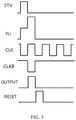
- FIG. 3 is a timing sequence diagram of signals in the circuit diagram as shown in FIG. 2 .
- TFTs thin-film transistors
- the TFTs may also be P-type transistors.
- the pull-down circuit 2 may include a first sub-circuit 21, a second sub-circuit 22 and a third sub-circuit 23.
- a first end of the first sub-circuit 21 is connected with a control end of the driver circuit 1; a second end of the first sub-circuit 21 is connected with a low-voltage end VSS; and a third end of the first sub-circuit 21 is connected with the second sub-circuit 22 and the third sub-circuit 23.
- a first end of the second sub-circuit 22 is connected with a signal input end; a second end of the second sub-circuit 22 is connected with a second clock signal CLKB; and a third end of the second sub-circuit 22 is connected with the third end of the first sub-circuit 21.
- a first end of the third sub-circuit 23 is connected with the low-voltage end VSS; a second end of the third sub-circuit 23 is connected with the control end of the driver circuit 1; and a third end of the third sub-circuit 23 is connected with the third end of the first sub-circuit 21.
- the signal input end may be a high-voltage end VGH, or the second clock signal CLKB may be inputted from the signal input end.
- the first sub-circuit 21 may include a fourth transistor M4.
- a control electrode of the fourth transistor M4 is the third end of the first sub-circuit 21 and connected with the second sub-circuit 22 and the third sub-circuit 23;
- a source electrode of the fourth transistor M4 is the second end of the first sub-circuit 21 and connected with the low-voltage end VSS;
- a drain electrode of the fourth transistor M4 is the first end of the first sub-circuit 21 and connected with the control end of the driver circuit 1.
- the second sub-circuit 22 may include a first transistor M1 and a second transistor M2.
- a control electrode of the first transistor M1 is the second end of the second sub-circuit 22 and connected with the second clock signal CLKB;
- a source electrode of the first transistor M1 is the first end of the second sub-circuit 22 and connected with the signal input end (namely the high-voltage end VGH); and
- a drain electrode of the first transistor M1 is connected with a control electrode and a source electrode of the second transistor M2.
- a drain electrode of the second transistor M2 is the third end of the second sub-circuit 22 and connected with the third end of the first sub-circuit 21.
- the third sub-circuit 23 may include a third transistor M3.
- a control electrode of the third transistor M3 is the second end of the third sub-circuit 23 and connected with the control end of the driver circuit 1;
- a source electrode of the third transistor M3 is the first end of the third sub-circuit 23 and connected with the low-voltage end VSS; and
- a drain electrode of the third transistor M3 is the third end of the third sub-circuit 23 and connected with the third end of the first sub-circuit 21.
- the driver circuit 1 may include a driving transistor M7.
- a control electrode of the driving transistor M7 is the control end of the driver circuit 1 and connected with an output end of the pull-up circuit 3; a source electrode of the driving transistor M7 is connected with the first clock signal CLK; and a drain electrode of the driving transistor M7 is connected with the output end OUTPUT of the GOA unit.
- the pull-up circuit 3 may include a sixth transistor M6 and a first capacitor C1.
- a control electrode and a source electrode of the sixth transistor M6 are connected with a pull-up signal, and a drain electrode of the sixth transistor M6 is connected with the control electrode of the driving transistor M7.
- a first end of the first capacitor C1 is connected between the drain electrode of the sixth transistor M6 and the control electrode of the driving transistor M7, and a second end of the first capacitor C1 is connected with the output end OUTPUT of the GOA unit.
- the reset circuit 4 may include an eighth transistor M8 and a ninth transistor M9.
- a control electrode of the eighth transistor M8 is connected with a signal reset end Reset; a source electrode of the eighth transistor M8 is connected with the low-voltage end VSS; and a drain electrode of the eighth transistor M8 is connected with the control electrode of the driving transistor M7.
- a control electrode of the ninth transistor M9 is connected with the signal reset end Reset; a source electrode of the ninth transistor M9 is connected with the low-voltage end VSS; and a drain electrode of the ninth transistor M9 is connected with the output end OUTPUT of the GOA unit.
- An operating process of elements in the GOA unit provided by the embodiments of the present disclosure may include a first period, a second period, a third period and a fourth period.
- the second clock signal CLKB is in a high level, so that the first transistor M1 and the second transistor M2 can be switched on.
- the reset signal Reset is in a low level, so that the eighth transistor M8 and the ninth transistor M9 can be switched off.
- the pull-up signal (which is an STV signal here and indicates that the GOA unit is disposed on the first row of the gate driver circuit) is in a high level and configured to pull up the electric potential of the pull-up node PU.
- the first end of the first capacitor C1 is charged, so that the driving transistor M7 is switched on, and hence the first clock signal CLK is outputted from the output end OUTPUT through the driving transistor M7 and inputted into the second end of the first capacitor.
- the third transistor M3 is switched on, so that the control electrode of the fourth transistor M4 is connected with the low-voltage end VSS, and hence the fourth transistor M4 is switched off in the first period.
- the STV signal is changed to a low level, so that the sixth transistor M6 is switched off, and hence the pull-up node PU maintains a high level and is in the flooding state, the first clock signal CLK is changed from the low level to the high level, so that the output end OUTPUT of the GOA unit outputs a high level signal.
- the second end of the first capacitor C1 is charged so that the first capacitor C1 is subjected to bootstrapping, and hence the electric potential of the pull-up node PU can be further increased.
- the reset signal Reset is changed to from a low level to a high level, so that the eighth transistor M8 and the ninth transistor M9 can be switched on, and hence the pull-up node PU is connected with the low-voltage end VSS and the output end OUTPUT of the GOA unit is also connected with the low-voltage end VSS.
- the driving transistor M7 is switched off and the GOA unit outputs the off signal.
- the second clock signal CLKB is in high level, so that the first transistor M1 and the second transistor M2 can be switched on, and hence the electric potential of the control electrode of the fourth transistor M4 is in high level and the fourth transistor M4 is switched on.
- the low-voltage end VSS is connected with the control electrode of the driving transistor M7 through the fourth transistor M4, so that the driving transistor M7 can keep the off state in this period and cannot be incorrectly switched on by a signal which is coupled into the GOA unit.
- the GOA does not output incorrect driving signals.
- one row of pixels corresponding to the GOA unit cannot be incorrectly switched on and display incorrect images.
- the circuit structure of the GOA unit is not limited to the structure as shown in FIG. 2 .
- FIG. 4 is a circuit diagram of the GOA unit provided by an embodiment of the present disclosure.
- the pull-down unit 2 further includes a fourth sub-circuit 24.
- a first end of the fourth sub-circuit 24 is connected with the output end OUTPUT of the GOA unit; a second end of the fourth sub-circuit 24 is connected with the low-voltage end VSS; and a third end of the fourth sub-circuit 24 is connected with the third end of the second sub-circuit 22 and the third end of the third sub-circuit 23.
- the fourth sub-circuit 24 may include a fifth transistor M5.
- a control electrode of the fifth transistor M5 is the third end of the fourth sub-circuit 24 and connected with the drain electrode of the second transistor M2 in the second sub-circuit 22 and the drain electrode of the third transistor M3 in the third sub-circuit 23; a source electrode of the fifth transistor M5 is the second end of the fourth sub-circuit 24 and connected with the low-voltage end VSS; and a drain electrode of the fifth transistor M5 is the first end of the fourth sub-circuit 24 and connected with the output end OUTPUT of the GOA unit.
- both the second end of the first capacitor C1 and the output end OUTPUT are connected with the low-voltage end VSS, so that the signal outputted from the output end OUTPUT of the GOA unit is further guaranteed to be an off signal, and hence the adverse effect of the signal which is coupled into the GOA unit can be maximally reduced on the GOA unit.
- the low-voltage ends connected with the third transistor M3, the fourth transistor M4 and the fifth transistor M5 are the same low-voltage end so as to reduce the number of power ports needed to be arranged.
- the low-voltage end connected with the pull-down circuit 2 and the low-voltage end connected with the reset circuit 4 have the same voltage so as to reduce the number of the power ports needed to be arranged.
- the pull-down circuit 2 may also be connected with a plurality of low-voltage ends.
- the source electrode of the third transistor M3 is connected with a first low-voltage end VSS1
- the source electrode of the fourth transistor M4 is connected with a second low-voltage end VSS2.
- the source electrode of the third transistor M3 is connected with the first low-voltage end VSS1
- both the source electrode of the fourth transistor M4 and the source electrode of the fifth transistor M5 are connected with the second low-voltage end VSS2.
- the low-voltage end connected with the source electrode of the fourth transistor M4 and the low-voltage end connected with the source electrode of the fifth transistor M5 may also be different low-voltage ends.
- a low-voltage signal is inputted into the control electrode of the driving transistor M7 from the low-voltage end connected with the source electrode of the fourth transistor M4.
- the low-voltage end connected with the pull-down circuit 2 and the low-voltage end connected with the reset circuit 4 may be different low-voltage ends, as long as the low-voltage signals outputted by the low-voltage ends that are connected with the pull-down circuit 2 or the reset circuit 4 can drive the driving transistor M7 to be switched off.
- a voltage inputted from the signal input end may be equal to a turn-on voltage of the gate driver circuit.
- a voltage outputted from the high-voltage end VGH may be equal to the turn-on voltage of the gate driver circuit.
- a signal waveform of the second clock signal CLKB is not limited to the waveform as shown in FIG. 3 , as long as the voltage of the control electrode of the fourth transistor M4 is in low level when the pull-up node PU is in high level (as for an embodiment in which the pull-down circuit 2 includes the fifth transistor M5, the voltage of the control electrode of the fifth transistor M5 may also need to be pulled down to low level).
- the pull-down circuit 2 allows the control end of the driver circuit 1 to be connected with the low-voltage end VSS, and the low-voltage signal is inputted into the control end of the driver circuit 1 from the low-voltage end VSS.
- the driver circuit 1 can keep the off state when the GOA unit outputs the off signal, and hence a scenario that the driver circuit 1 is switched on by a signal which is coupled into the GOA unit due to signal crosstalk can be avoided.
- the GOA unit may also maintain the state of outputting the off signal and may not incorrectly output the driving signal as in the existing technologies, so that the incorrect switching-on of one row of pixels corresponding to the GOA unit can be avoided.
- the row of pixels cannot be charged and display incorrect images, and hence the "abnormal image" phenomenon can be overcome.
- the embodiments of the present disclosure further provide a gate driver circuit, which comprises the GOA unit provided by the above-described embodiments.
- the gate driver circuit provided by the embodiments adopt the GOA unit provided by the above-described embodiments and can avoid the incorrect switching-on of various rows of pixels corresponding to various stages of GOA units respectively, so that various rows of pixels cannot be charged and display incorrect images, and hence the "abnormal image" phenomenon can be overcome.
- the embodiments of the present disclosure further provide a display device, which comprises the gate driver circuit provided by the above-described embodiments.
- the display device provided by the embodiments adopts the gate driver circuit in the above embodiments and can avoid the incorrect switching-on of various rows of pixels corresponding to various stages of GOA units respectively, so that various rows of pixels cannot be charged and display incorrect images, and hence the "abnormal image” phenomenon can be overcome.
Applications Claiming Priority (2)
| Application Number | Priority Date | Filing Date | Title |
|---|---|---|---|
| CN201510614177.5A CN105096811B (zh) | 2015-09-23 | 2015-09-23 | Goa单元、栅极驱动电路及显示装置 |
| PCT/CN2016/073981 WO2017049853A1 (fr) | 2015-09-23 | 2016-02-18 | Unité de goa, circuit de pilotage de grille et dispositif d'affichage |
Publications (2)
| Publication Number | Publication Date |
|---|---|
| EP3355295A1 true EP3355295A1 (fr) | 2018-08-01 |
| EP3355295A4 EP3355295A4 (fr) | 2019-03-20 |
Family
ID=54577107
Family Applications (1)
| Application Number | Title | Priority Date | Filing Date |
|---|---|---|---|
| EP16822364.2A Withdrawn EP3355295A4 (fr) | 2015-09-23 | 2016-02-18 | Unité de goa, circuit de pilotage de grille et dispositif d'affichage |
Country Status (4)
| Country | Link |
|---|---|
| US (1) | US20170301277A1 (fr) |
| EP (1) | EP3355295A4 (fr) |
| CN (1) | CN105096811B (fr) |
| WO (1) | WO2017049853A1 (fr) |
Families Citing this family (7)
| Publication number | Priority date | Publication date | Assignee | Title |
|---|---|---|---|---|
| CN105096811B (zh) * | 2015-09-23 | 2017-12-08 | 京东方科技集团股份有限公司 | Goa单元、栅极驱动电路及显示装置 |
| US11127336B2 (en) | 2015-09-23 | 2021-09-21 | Boe Technology Group Co., Ltd. | Gate on array (GOA) unit, gate driver circuit and display device |
| CN107016972B (zh) * | 2017-04-25 | 2019-08-02 | 深圳市华星光电技术有限公司 | Goa驱动电路和液晶显示面板 |
| US10460671B2 (en) * | 2017-07-04 | 2019-10-29 | Shenzhen China Star Optoelectronics Semiconductor Display Technology Co., Lltd | Scanning driving circuit and display apparatus |
| CN108735176B (zh) * | 2018-06-06 | 2020-01-03 | 京东方科技集团股份有限公司 | 栅极驱动单元及其驱动方法、栅极驱动电路和显示装置 |
| CN108648715B (zh) * | 2018-07-17 | 2020-02-04 | 惠科股份有限公司 | 移位暂存器、显示面板、以及移位暂存器的驱动方法 |
| CN113808533B (zh) * | 2021-09-15 | 2023-06-02 | 深圳市华星光电半导体显示技术有限公司 | 显示面板及显示终端 |
Family Cites Families (34)
| Publication number | Priority date | Publication date | Assignee | Title |
|---|---|---|---|---|
| JP5079350B2 (ja) * | 2006-04-25 | 2012-11-21 | 三菱電機株式会社 | シフトレジスタ回路 |
| JP2007317288A (ja) * | 2006-05-25 | 2007-12-06 | Mitsubishi Electric Corp | シフトレジスタ回路およびそれを備える画像表示装置 |
| JP4912186B2 (ja) * | 2007-03-05 | 2012-04-11 | 三菱電機株式会社 | シフトレジスタ回路およびそれを備える画像表示装置 |
| TWI407443B (zh) * | 2009-03-05 | 2013-09-01 | Au Optronics Corp | 移位暫存器 |
| CN102012591B (zh) * | 2009-09-04 | 2012-05-30 | 北京京东方光电科技有限公司 | 移位寄存器单元及液晶显示器栅极驱动装置 |
| CN102237029B (zh) * | 2010-04-23 | 2013-05-29 | 北京京东方光电科技有限公司 | 移位寄存器、液晶显示器栅极驱动装置和数据线驱动装置 |
| CN102651186B (zh) * | 2011-04-07 | 2015-04-01 | 北京京东方光电科技有限公司 | 移位寄存器及栅线驱动装置 |
| KR101768485B1 (ko) * | 2011-04-21 | 2017-08-31 | 엘지디스플레이 주식회사 | 쉬프트 레지스터 |
| CN102682689B (zh) * | 2012-04-13 | 2014-11-26 | 京东方科技集团股份有限公司 | 一种移位寄存器、栅极驱动电路及显示装置 |
| CN102930812B (zh) * | 2012-10-09 | 2015-08-19 | 北京京东方光电科技有限公司 | 移位寄存器、栅线集成驱动电路、阵列基板及显示器 |
| KR102066083B1 (ko) * | 2013-01-31 | 2020-01-15 | 엘지디스플레이 주식회사 | 쉬프트 레지스터 |
| CN103258495B (zh) * | 2013-05-07 | 2015-08-05 | 京东方科技集团股份有限公司 | 移位寄存单元、移位寄存器和显示装置 |
| CN103345941B (zh) * | 2013-07-03 | 2016-12-28 | 京东方科技集团股份有限公司 | 移位寄存器单元及驱动方法、移位寄存器电路及显示装置 |
| CN103413531B (zh) * | 2013-07-22 | 2015-12-09 | 北京京东方光电科技有限公司 | 一种移位寄存器单元、栅极驱动电路及显示器件 |
| CN103440839B (zh) * | 2013-08-09 | 2016-03-23 | 京东方科技集团股份有限公司 | 移位寄存单元、移位寄存器和显示装置 |
| US9437324B2 (en) * | 2013-08-09 | 2016-09-06 | Boe Technology Group Co., Ltd. | Shift register unit, driving method thereof, shift register and display device |
| CN103680453B (zh) * | 2013-12-20 | 2015-09-16 | 深圳市华星光电技术有限公司 | 阵列基板行驱动电路 |
| CN103700356A (zh) * | 2013-12-27 | 2014-04-02 | 合肥京东方光电科技有限公司 | 移位寄存器单元及其驱动方法、移位寄存器、显示装置 |
| TW201535975A (zh) * | 2014-03-10 | 2015-09-16 | Chunghwa Picture Tubes Ltd | 閘極驅動電路 |
| CN104091574B (zh) * | 2014-06-25 | 2016-03-02 | 京东方科技集团股份有限公司 | 移位寄存器、阵列基板、显示装置及其驱动方法 |
| KR102175403B1 (ko) * | 2014-07-21 | 2020-11-06 | 한국전자통신연구원 | 디지털 연산 회로의 기능 복구 장치 및 방법 |
| CN104361869A (zh) * | 2014-10-31 | 2015-02-18 | 京东方科技集团股份有限公司 | 移位寄存器单元电路、移位寄存器、驱动方法及显示装置 |
| CN104318886B (zh) * | 2014-10-31 | 2017-04-05 | 京东方科技集团股份有限公司 | 一种goa单元及驱动方法,goa电路和显示装置 |
| CN104505049B (zh) * | 2014-12-31 | 2017-04-19 | 深圳市华星光电技术有限公司 | 一种栅极驱动电路 |
| CN104732939A (zh) * | 2015-03-27 | 2015-06-24 | 京东方科技集团股份有限公司 | 移位寄存器、栅极驱动电路、显示装置及栅极驱动方法 |
| CN104766580B (zh) * | 2015-04-23 | 2017-08-01 | 合肥京东方光电科技有限公司 | 移位寄存器单元及驱动方法、栅极驱动电路和显示装置 |
| CN104835476B (zh) * | 2015-06-08 | 2017-09-15 | 京东方科技集团股份有限公司 | 移位寄存器单元、栅极驱动电路及其驱动方法、阵列基板 |
| CN104867472B (zh) * | 2015-06-15 | 2017-10-17 | 合肥京东方光电科技有限公司 | 一种移位寄存器单元、栅极驱动电路和显示装置 |
| CN104952409B (zh) * | 2015-07-07 | 2018-12-28 | 京东方科技集团股份有限公司 | 栅极驱动单元及其驱动方法、栅极驱动电路和显示装置 |
| USPP28833P3 (en) * | 2015-09-11 | 2018-01-02 | Sunview Vineyards Of California, Inc. | Grapevine named ‘SV22-104e-84’ |
| CN105096811B (zh) * | 2015-09-23 | 2017-12-08 | 京东方科技集团股份有限公司 | Goa单元、栅极驱动电路及显示装置 |
| CN204966012U (zh) * | 2015-09-23 | 2016-01-13 | 京东方科技集团股份有限公司 | Goa单元、栅极驱动电路及显示装置 |
| CN105139822B (zh) * | 2015-09-30 | 2017-11-10 | 上海中航光电子有限公司 | 移位寄存器及其驱动方法,栅极驱动电路 |
| CN105185320B (zh) * | 2015-10-23 | 2017-12-08 | 京东方科技集团股份有限公司 | 一种goa单元、goa电路、显示驱动电路和显示装置 |
-
2015
- 2015-09-23 CN CN201510614177.5A patent/CN105096811B/zh active Active
-
2016
- 2016-02-18 US US15/324,881 patent/US20170301277A1/en not_active Abandoned
- 2016-02-18 WO PCT/CN2016/073981 patent/WO2017049853A1/fr active Application Filing
- 2016-02-18 EP EP16822364.2A patent/EP3355295A4/fr not_active Withdrawn
Also Published As
| Publication number | Publication date |
|---|---|
| WO2017049853A1 (fr) | 2017-03-30 |
| CN105096811A (zh) | 2015-11-25 |
| US20170301277A1 (en) | 2017-10-19 |
| EP3355295A4 (fr) | 2019-03-20 |
| CN105096811B (zh) | 2017-12-08 |
Similar Documents
| Publication | Publication Date | Title |
|---|---|---|
| US10803823B2 (en) | Shift register unit, gate driving circuit, and driving method | |
| US10269282B2 (en) | Shift register, gate driving circuit, display panel and driving method | |
| US9791968B2 (en) | Shift register, its driving method, gate driver circuit and display device | |
| EP3355295A1 (fr) | Unité de goa, circuit de pilotage de grille et dispositif d'affichage | |
| US9177666B2 (en) | Shift register unit and driving method thereof, shift register and display apparatus | |
| US11688326B2 (en) | Shift register, gate driving circuit, display apparatus and driving method | |
| US10593279B2 (en) | Display device, gate driving circuit and gate driving unit | |
| US9881688B2 (en) | Shift register | |
| US20180122289A1 (en) | Shift register, driving method, gate driving circuit and display device | |
| US20140064438A1 (en) | Shift Register, Gate Driving Circuit And Display | |
| CN114677965A (zh) | 移位寄存器单元、栅极驱动电路及显示装置 | |
| US11456045B2 (en) | Shift register, driving method thereof, gate driving circuit, and display apparatus | |
| US10043585B2 (en) | Shift register unit, gate drive device, display device, and control method | |
| EP3712880B1 (fr) | Circuit d'attaque de grille, dispositif d'affichage et procédé d'attaque associé | |
| EP3041000A1 (fr) | Unité de registre à décalage, registre à décalage et dispositif d'affichage | |
| CN107123391B (zh) | 栅极驱动单元及其驱动方法、栅极驱动电路和显示装置 | |
| US10825371B2 (en) | Shift register, gate driving circuit, display panel and driving method | |
| US11094389B2 (en) | Shift register unit and driving method, gate driving circuit, and display device | |
| US11450252B2 (en) | Shift register, gate driving circuit, display apparatus and driving method | |
| US20200302845A1 (en) | Shift register unit, driving method thereof, gate driver on array and display apparatus | |
| CN111210789B (zh) | 移位寄存器及驱动方法、栅极驱动电路、显示面板 | |
| US10971102B2 (en) | Shift register unit and driving method, gate driving circuit, and display device | |
| US11127336B2 (en) | Gate on array (GOA) unit, gate driver circuit and display device | |
| CN116343666A (zh) | 显示面板及其驱动方法、显示装置 |
Legal Events
| Date | Code | Title | Description |
|---|---|---|---|
| STAA | Information on the status of an ep patent application or granted ep patent |
Free format text: STATUS: UNKNOWN |
|
| STAA | Information on the status of an ep patent application or granted ep patent |
Free format text: STATUS: THE INTERNATIONAL PUBLICATION HAS BEEN MADE |
|
| PUAI | Public reference made under article 153(3) epc to a published international application that has entered the european phase |
Free format text: ORIGINAL CODE: 0009012 |
|
| STAA | Information on the status of an ep patent application or granted ep patent |
Free format text: STATUS: REQUEST FOR EXAMINATION WAS MADE |
|
| 17P | Request for examination filed |
Effective date: 20170116 |
|
| AK | Designated contracting states |
Kind code of ref document: A1 Designated state(s): AL AT BE BG CH CY CZ DE DK EE ES FI FR GB GR HR HU IE IS IT LI LT LU LV MC MK MT NL NO PL PT RO RS SE SI SK SM TR |
|
| AX | Request for extension of the european patent |
Extension state: BA ME |
|
| DAV | Request for validation of the european patent (deleted) | ||
| DAX | Request for extension of the european patent (deleted) | ||
| A4 | Supplementary search report drawn up and despatched |
Effective date: 20190218 |
|
| RIC1 | Information provided on ipc code assigned before grant |
Ipc: G11C 19/18 20060101ALI20190212BHEP Ipc: G09G 3/20 20060101AFI20190212BHEP |
|
| STAA | Information on the status of an ep patent application or granted ep patent |
Free format text: STATUS: EXAMINATION IS IN PROGRESS |
|
| 17Q | First examination report despatched |
Effective date: 20191127 |
|
| STAA | Information on the status of an ep patent application or granted ep patent |
Free format text: STATUS: EXAMINATION IS IN PROGRESS |
|
| STAA | Information on the status of an ep patent application or granted ep patent |
Free format text: STATUS: EXAMINATION IS IN PROGRESS |
|
| STAA | Information on the status of an ep patent application or granted ep patent |
Free format text: STATUS: THE APPLICATION IS DEEMED TO BE WITHDRAWN |
|
| 18D | Application deemed to be withdrawn |
Effective date: 20220301 |