EP3351068B1 - Mediendichtes steuergerät für ein kraftfahrzeug und verfahren zur herstellung des steuergerätes - Google Patents
Mediendichtes steuergerät für ein kraftfahrzeug und verfahren zur herstellung des steuergerätes Download PDFInfo
- Publication number
- EP3351068B1 EP3351068B1 EP16758106.5A EP16758106A EP3351068B1 EP 3351068 B1 EP3351068 B1 EP 3351068B1 EP 16758106 A EP16758106 A EP 16758106A EP 3351068 B1 EP3351068 B1 EP 3351068B1
- Authority
- EP
- European Patent Office
- Prior art keywords
- housing cover
- control device
- circuit board
- printed circuit
- cavity
- Prior art date
- Legal status (The legal status is an assumption and is not a legal conclusion. Google has not performed a legal analysis and makes no representation as to the accuracy of the status listed.)
- Active
Links
- 238000004519 manufacturing process Methods 0.000 title claims description 6
- 229920000642 polymer Polymers 0.000 claims description 26
- 230000001681 protective effect Effects 0.000 claims description 19
- 239000004020 conductor Substances 0.000 claims description 13
- 238000000034 method Methods 0.000 claims description 11
- 239000000853 adhesive Substances 0.000 claims description 7
- 230000001070 adhesive effect Effects 0.000 claims description 7
- 229910052751 metal Inorganic materials 0.000 claims description 7
- 239000002184 metal Substances 0.000 claims description 7
- 238000005538 encapsulation Methods 0.000 claims description 5
- 239000004033 plastic Substances 0.000 claims description 5
- 229920003023 plastic Polymers 0.000 claims description 5
- 239000002861 polymer material Substances 0.000 claims description 5
- 239000012778 molding material Substances 0.000 claims description 4
- 238000004026 adhesive bonding Methods 0.000 claims description 3
- 229910052782 aluminium Inorganic materials 0.000 claims description 3
- XAGFODPZIPBFFR-UHFFFAOYSA-N aluminium Chemical compound [Al] XAGFODPZIPBFFR-UHFFFAOYSA-N 0.000 claims description 3
- 239000011347 resin Substances 0.000 claims description 3
- 229920005989 resin Polymers 0.000 claims description 3
- 238000005476 soldering Methods 0.000 claims description 3
- 230000002093 peripheral effect Effects 0.000 claims 10
- 238000001746 injection moulding Methods 0.000 claims 4
- 238000003855 Adhesive Lamination Methods 0.000 claims 1
- 239000007789 gas Substances 0.000 description 11
- 230000005540 biological transmission Effects 0.000 description 7
- PCHJSUWPFVWCPO-UHFFFAOYSA-N gold Chemical compound [Au] PCHJSUWPFVWCPO-UHFFFAOYSA-N 0.000 description 6
- 239000000463 material Substances 0.000 description 6
- 239000010931 gold Substances 0.000 description 5
- 229910052737 gold Inorganic materials 0.000 description 5
- 239000003921 oil Substances 0.000 description 5
- 229920002430 Fibre-reinforced plastic Polymers 0.000 description 4
- 238000013461 design Methods 0.000 description 4
- 239000011151 fibre-reinforced plastic Substances 0.000 description 4
- 230000008569 process Effects 0.000 description 4
- 239000000126 substance Substances 0.000 description 4
- 239000003990 capacitor Substances 0.000 description 3
- 238000000465 moulding Methods 0.000 description 3
- 238000007789 sealing Methods 0.000 description 3
- 150000003568 thioethers Chemical class 0.000 description 3
- 230000015572 biosynthetic process Effects 0.000 description 2
- 239000000919 ceramic Substances 0.000 description 2
- 150000001875 compounds Chemical class 0.000 description 2
- 230000017525 heat dissipation Effects 0.000 description 2
- 238000003475 lamination Methods 0.000 description 2
- 239000011226 reinforced ceramic Substances 0.000 description 2
- 150000003839 salts Chemical class 0.000 description 2
- 229910001220 stainless steel Inorganic materials 0.000 description 2
- 239000010935 stainless steel Substances 0.000 description 2
- 150000003464 sulfur compounds Chemical class 0.000 description 2
- 239000004642 Polyimide Substances 0.000 description 1
- BQCADISMDOOEFD-UHFFFAOYSA-N Silver Chemical compound [Ag] BQCADISMDOOEFD-UHFFFAOYSA-N 0.000 description 1
- 239000000969 carrier Substances 0.000 description 1
- 230000008859 change Effects 0.000 description 1
- 238000006243 chemical reaction Methods 0.000 description 1
- 238000010276 construction Methods 0.000 description 1
- 238000005260 corrosion Methods 0.000 description 1
- 230000007797 corrosion Effects 0.000 description 1
- 238000011161 development Methods 0.000 description 1
- 238000009792 diffusion process Methods 0.000 description 1
- 230000007613 environmental effect Effects 0.000 description 1
- 238000011156 evaluation Methods 0.000 description 1
- 238000007765 extrusion coating Methods 0.000 description 1
- 239000012530 fluid Substances 0.000 description 1
- 239000012208 gear oil Substances 0.000 description 1
- 239000011521 glass Substances 0.000 description 1
- 230000010354 integration Effects 0.000 description 1
- 229920001721 polyimide Polymers 0.000 description 1
- 238000012545 processing Methods 0.000 description 1
- 230000009467 reduction Effects 0.000 description 1
- 229910052709 silver Inorganic materials 0.000 description 1
- 239000004332 silver Substances 0.000 description 1
- 239000000758 substrate Substances 0.000 description 1
- 238000003466 welding Methods 0.000 description 1
Images


Classifications
-
- H—ELECTRICITY
- H05—ELECTRIC TECHNIQUES NOT OTHERWISE PROVIDED FOR
- H05K—PRINTED CIRCUITS; CASINGS OR CONSTRUCTIONAL DETAILS OF ELECTRIC APPARATUS; MANUFACTURE OF ASSEMBLAGES OF ELECTRICAL COMPONENTS
- H05K5/00—Casings, cabinets or drawers for electric apparatus
- H05K5/06—Hermetically-sealed casings
- H05K5/065—Hermetically-sealed casings sealed by encapsulation, e.g. waterproof resin forming an integral casing, injection moulding
-
- H—ELECTRICITY
- H05—ELECTRIC TECHNIQUES NOT OTHERWISE PROVIDED FOR
- H05K—PRINTED CIRCUITS; CASINGS OR CONSTRUCTIONAL DETAILS OF ELECTRIC APPARATUS; MANUFACTURE OF ASSEMBLAGES OF ELECTRICAL COMPONENTS
- H05K5/00—Casings, cabinets or drawers for electric apparatus
- H05K5/0026—Casings, cabinets or drawers for electric apparatus provided with connectors and printed circuit boards [PCB], e.g. automotive electronic control units
- H05K5/0082—Casings, cabinets or drawers for electric apparatus provided with connectors and printed circuit boards [PCB], e.g. automotive electronic control units specially adapted for transmission control units, e.g. gearbox controllers
-
- H—ELECTRICITY
- H05—ELECTRIC TECHNIQUES NOT OTHERWISE PROVIDED FOR
- H05K—PRINTED CIRCUITS; CASINGS OR CONSTRUCTIONAL DETAILS OF ELECTRIC APPARATUS; MANUFACTURE OF ASSEMBLAGES OF ELECTRICAL COMPONENTS
- H05K1/00—Printed circuits
- H05K1/02—Details
- H05K1/14—Structural association of two or more printed circuits
- H05K1/142—Arrangements of planar printed circuit boards in the same plane, e.g. auxiliary printed circuit insert mounted in a main printed circuit
-
- H—ELECTRICITY
- H05—ELECTRIC TECHNIQUES NOT OTHERWISE PROVIDED FOR
- H05K—PRINTED CIRCUITS; CASINGS OR CONSTRUCTIONAL DETAILS OF ELECTRIC APPARATUS; MANUFACTURE OF ASSEMBLAGES OF ELECTRICAL COMPONENTS
- H05K1/00—Printed circuits
- H05K1/18—Printed circuits structurally associated with non-printed electric components
- H05K1/181—Printed circuits structurally associated with non-printed electric components associated with surface mounted components
-
- H—ELECTRICITY
- H05—ELECTRIC TECHNIQUES NOT OTHERWISE PROVIDED FOR
- H05K—PRINTED CIRCUITS; CASINGS OR CONSTRUCTIONAL DETAILS OF ELECTRIC APPARATUS; MANUFACTURE OF ASSEMBLAGES OF ELECTRICAL COMPONENTS
- H05K1/00—Printed circuits
- H05K1/18—Printed circuits structurally associated with non-printed electric components
- H05K1/189—Printed circuits structurally associated with non-printed electric components characterised by the use of a flexible or folded printed circuit
-
- H—ELECTRICITY
- H05—ELECTRIC TECHNIQUES NOT OTHERWISE PROVIDED FOR
- H05K—PRINTED CIRCUITS; CASINGS OR CONSTRUCTIONAL DETAILS OF ELECTRIC APPARATUS; MANUFACTURE OF ASSEMBLAGES OF ELECTRICAL COMPONENTS
- H05K3/00—Apparatus or processes for manufacturing printed circuits
- H05K3/22—Secondary treatment of printed circuits
- H05K3/28—Applying non-metallic protective coatings
- H05K3/284—Applying non-metallic protective coatings for encapsulating mounted components
-
- H—ELECTRICITY
- H05—ELECTRIC TECHNIQUES NOT OTHERWISE PROVIDED FOR
- H05K—PRINTED CIRCUITS; CASINGS OR CONSTRUCTIONAL DETAILS OF ELECTRIC APPARATUS; MANUFACTURE OF ASSEMBLAGES OF ELECTRICAL COMPONENTS
- H05K5/00—Casings, cabinets or drawers for electric apparatus
- H05K5/0017—Casings, cabinets or drawers for electric apparatus with operator interface units
-
- H—ELECTRICITY
- H05—ELECTRIC TECHNIQUES NOT OTHERWISE PROVIDED FOR
- H05K—PRINTED CIRCUITS; CASINGS OR CONSTRUCTIONAL DETAILS OF ELECTRIC APPARATUS; MANUFACTURE OF ASSEMBLAGES OF ELECTRICAL COMPONENTS
- H05K5/00—Casings, cabinets or drawers for electric apparatus
- H05K5/02—Details
- H05K5/0247—Electrical details of casings, e.g. terminals, passages for cables or wiring
-
- H—ELECTRICITY
- H05—ELECTRIC TECHNIQUES NOT OTHERWISE PROVIDED FOR
- H05K—PRINTED CIRCUITS; CASINGS OR CONSTRUCTIONAL DETAILS OF ELECTRIC APPARATUS; MANUFACTURE OF ASSEMBLAGES OF ELECTRICAL COMPONENTS
- H05K5/00—Casings, cabinets or drawers for electric apparatus
- H05K5/02—Details
- H05K5/03—Covers
-
- H—ELECTRICITY
- H01—ELECTRIC ELEMENTS
- H01L—SEMICONDUCTOR DEVICES NOT COVERED BY CLASS H10
- H01L21/00—Processes or apparatus adapted for the manufacture or treatment of semiconductor or solid state devices or of parts thereof
- H01L21/02—Manufacture or treatment of semiconductor devices or of parts thereof
- H01L21/04—Manufacture or treatment of semiconductor devices or of parts thereof the devices having potential barriers, e.g. a PN junction, depletion layer or carrier concentration layer
- H01L21/50—Assembly of semiconductor devices using processes or apparatus not provided for in a single one of the subgroups H01L21/06 - H01L21/326, e.g. sealing of a cap to a base of a container
- H01L21/56—Encapsulations, e.g. encapsulation layers, coatings
-
- H—ELECTRICITY
- H01—ELECTRIC ELEMENTS
- H01L—SEMICONDUCTOR DEVICES NOT COVERED BY CLASS H10
- H01L2224/00—Indexing scheme for arrangements for connecting or disconnecting semiconductor or solid-state bodies and methods related thereto as covered by H01L24/00
- H01L2224/01—Means for bonding being attached to, or being formed on, the surface to be connected, e.g. chip-to-package, die-attach, "first-level" interconnects; Manufacturing methods related thereto
- H01L2224/42—Wire connectors; Manufacturing methods related thereto
- H01L2224/47—Structure, shape, material or disposition of the wire connectors after the connecting process
- H01L2224/48—Structure, shape, material or disposition of the wire connectors after the connecting process of an individual wire connector
- H01L2224/4805—Shape
- H01L2224/4809—Loop shape
- H01L2224/48091—Arched
-
- H—ELECTRICITY
- H01—ELECTRIC ELEMENTS
- H01L—SEMICONDUCTOR DEVICES NOT COVERED BY CLASS H10
- H01L23/00—Details of semiconductor or other solid state devices
- H01L23/28—Encapsulations, e.g. encapsulating layers, coatings, e.g. for protection
-
- H—ELECTRICITY
- H01—ELECTRIC ELEMENTS
- H01L—SEMICONDUCTOR DEVICES NOT COVERED BY CLASS H10
- H01L2924/00—Indexing scheme for arrangements or methods for connecting or disconnecting semiconductor or solid-state bodies as covered by H01L24/00
- H01L2924/15—Details of package parts other than the semiconductor or other solid state devices to be connected
- H01L2924/181—Encapsulation
-
- H—ELECTRICITY
- H01—ELECTRIC ELEMENTS
- H01L—SEMICONDUCTOR DEVICES NOT COVERED BY CLASS H10
- H01L2924/00—Indexing scheme for arrangements or methods for connecting or disconnecting semiconductor or solid-state bodies as covered by H01L24/00
- H01L2924/19—Details of hybrid assemblies other than the semiconductor or other solid state devices to be connected
- H01L2924/191—Disposition
- H01L2924/19101—Disposition of discrete passive components
- H01L2924/19107—Disposition of discrete passive components off-chip wires
-
- H—ELECTRICITY
- H05—ELECTRIC TECHNIQUES NOT OTHERWISE PROVIDED FOR
- H05K—PRINTED CIRCUITS; CASINGS OR CONSTRUCTIONAL DETAILS OF ELECTRIC APPARATUS; MANUFACTURE OF ASSEMBLAGES OF ELECTRICAL COMPONENTS
- H05K2201/00—Indexing scheme relating to printed circuits covered by H05K1/00
- H05K2201/07—Electric details
- H05K2201/0707—Shielding
-
- H—ELECTRICITY
- H05—ELECTRIC TECHNIQUES NOT OTHERWISE PROVIDED FOR
- H05K—PRINTED CIRCUITS; CASINGS OR CONSTRUCTIONAL DETAILS OF ELECTRIC APPARATUS; MANUFACTURE OF ASSEMBLAGES OF ELECTRICAL COMPONENTS
- H05K2201/00—Indexing scheme relating to printed circuits covered by H05K1/00
- H05K2201/09—Shape and layout
- H05K2201/09818—Shape or layout details not covered by a single group of H05K2201/09009 - H05K2201/09809
- H05K2201/0999—Circuit printed on or in housing, e.g. housing as PCB; Circuit printed on the case of a component; PCB affixed to housing
-
- H—ELECTRICITY
- H05—ELECTRIC TECHNIQUES NOT OTHERWISE PROVIDED FOR
- H05K—PRINTED CIRCUITS; CASINGS OR CONSTRUCTIONAL DETAILS OF ELECTRIC APPARATUS; MANUFACTURE OF ASSEMBLAGES OF ELECTRICAL COMPONENTS
- H05K2201/00—Indexing scheme relating to printed circuits covered by H05K1/00
- H05K2201/10—Details of components or other objects attached to or integrated in a printed circuit board
- H05K2201/10007—Types of components
- H05K2201/10015—Non-printed capacitor
-
- H—ELECTRICITY
- H05—ELECTRIC TECHNIQUES NOT OTHERWISE PROVIDED FOR
- H05K—PRINTED CIRCUITS; CASINGS OR CONSTRUCTIONAL DETAILS OF ELECTRIC APPARATUS; MANUFACTURE OF ASSEMBLAGES OF ELECTRICAL COMPONENTS
- H05K2201/00—Indexing scheme relating to printed circuits covered by H05K1/00
- H05K2201/10—Details of components or other objects attached to or integrated in a printed circuit board
- H05K2201/10007—Types of components
- H05K2201/1003—Non-printed inductor
-
- H—ELECTRICITY
- H05—ELECTRIC TECHNIQUES NOT OTHERWISE PROVIDED FOR
- H05K—PRINTED CIRCUITS; CASINGS OR CONSTRUCTIONAL DETAILS OF ELECTRIC APPARATUS; MANUFACTURE OF ASSEMBLAGES OF ELECTRICAL COMPONENTS
- H05K2201/00—Indexing scheme relating to printed circuits covered by H05K1/00
- H05K2201/10—Details of components or other objects attached to or integrated in a printed circuit board
- H05K2201/10227—Other objects, e.g. metallic pieces
- H05K2201/10287—Metal wires as connectors or conductors
-
- H—ELECTRICITY
- H05—ELECTRIC TECHNIQUES NOT OTHERWISE PROVIDED FOR
- H05K—PRINTED CIRCUITS; CASINGS OR CONSTRUCTIONAL DETAILS OF ELECTRIC APPARATUS; MANUFACTURE OF ASSEMBLAGES OF ELECTRICAL COMPONENTS
- H05K2201/00—Indexing scheme relating to printed circuits covered by H05K1/00
- H05K2201/10—Details of components or other objects attached to or integrated in a printed circuit board
- H05K2201/10227—Other objects, e.g. metallic pieces
- H05K2201/10371—Shields or metal cases
-
- H—ELECTRICITY
- H05—ELECTRIC TECHNIQUES NOT OTHERWISE PROVIDED FOR
- H05K—PRINTED CIRCUITS; CASINGS OR CONSTRUCTIONAL DETAILS OF ELECTRIC APPARATUS; MANUFACTURE OF ASSEMBLAGES OF ELECTRICAL COMPONENTS
- H05K2201/00—Indexing scheme relating to printed circuits covered by H05K1/00
- H05K2201/10—Details of components or other objects attached to or integrated in a printed circuit board
- H05K2201/10431—Details of mounted components
- H05K2201/10507—Involving several components
- H05K2201/10522—Adjacent components
-
- H—ELECTRICITY
- H05—ELECTRIC TECHNIQUES NOT OTHERWISE PROVIDED FOR
- H05K—PRINTED CIRCUITS; CASINGS OR CONSTRUCTIONAL DETAILS OF ELECTRIC APPARATUS; MANUFACTURE OF ASSEMBLAGES OF ELECTRICAL COMPONENTS
- H05K2203/00—Indexing scheme relating to apparatus or processes for manufacturing printed circuits covered by H05K3/00
- H05K2203/13—Moulding and encapsulation; Deposition techniques; Protective layers
- H05K2203/1305—Moulding and encapsulation
- H05K2203/1316—Moulded encapsulation of mounted components
-
- H—ELECTRICITY
- H05—ELECTRIC TECHNIQUES NOT OTHERWISE PROVIDED FOR
- H05K—PRINTED CIRCUITS; CASINGS OR CONSTRUCTIONAL DETAILS OF ELECTRIC APPARATUS; MANUFACTURE OF ASSEMBLAGES OF ELECTRICAL COMPONENTS
- H05K2203/00—Indexing scheme relating to apparatus or processes for manufacturing printed circuits covered by H05K3/00
- H05K2203/13—Moulding and encapsulation; Deposition techniques; Protective layers
- H05K2203/1305—Moulding and encapsulation
- H05K2203/1327—Moulding over PCB locally or completely
-
- H—ELECTRICITY
- H05—ELECTRIC TECHNIQUES NOT OTHERWISE PROVIDED FOR
- H05K—PRINTED CIRCUITS; CASINGS OR CONSTRUCTIONAL DETAILS OF ELECTRIC APPARATUS; MANUFACTURE OF ASSEMBLAGES OF ELECTRICAL COMPONENTS
- H05K9/00—Screening of apparatus or components against electric or magnetic fields
- H05K9/0007—Casings
- H05K9/002—Casings with localised screening
- H05K9/0022—Casings with localised screening of components mounted on printed circuit boards [PCB]
- H05K9/0024—Shield cases mounted on a PCB, e.g. cans or caps or conformal shields
-
- H—ELECTRICITY
- H05—ELECTRIC TECHNIQUES NOT OTHERWISE PROVIDED FOR
- H05K—PRINTED CIRCUITS; CASINGS OR CONSTRUCTIONAL DETAILS OF ELECTRIC APPARATUS; MANUFACTURE OF ASSEMBLAGES OF ELECTRICAL COMPONENTS
- H05K9/00—Screening of apparatus or components against electric or magnetic fields
- H05K9/0007—Casings
- H05K9/0052—Shielding other than Faraday cages
-
- H—ELECTRICITY
- H05—ELECTRIC TECHNIQUES NOT OTHERWISE PROVIDED FOR
- H05K—PRINTED CIRCUITS; CASINGS OR CONSTRUCTIONAL DETAILS OF ELECTRIC APPARATUS; MANUFACTURE OF ASSEMBLAGES OF ELECTRICAL COMPONENTS
- H05K9/00—Screening of apparatus or components against electric or magnetic fields
- H05K9/0071—Active shielding
-
- H—ELECTRICITY
- H05—ELECTRIC TECHNIQUES NOT OTHERWISE PROVIDED FOR
- H05K—PRINTED CIRCUITS; CASINGS OR CONSTRUCTIONAL DETAILS OF ELECTRIC APPARATUS; MANUFACTURE OF ASSEMBLAGES OF ELECTRICAL COMPONENTS
- H05K9/00—Screening of apparatus or components against electric or magnetic fields
- H05K9/0073—Shielding materials
- H05K9/0081—Electromagnetic shielding materials, e.g. EMI, RFI shielding
Definitions
- the invention relates to a control device for a motor vehicle and a method for its production according to the preamble of the independent claims.
- control devices In automotive engineering, components such as transmission, engine or brake systems are increasingly controlled electronically. There is a development towards integrated mechatronic controls, i.e. for the integration of control electronics and the associated electronic components such as sensors or valves in the transmission, the motor or the brake system. Control devices generally have a large number of electronic components that are connected to other components outside the control device. With such "on-site electronics", these controls are no longer housed in a separate, protected electronics room and must therefore withstand the corresponding environmental influences and mechanical, thermal and chemical stresses. For this purpose, they are usually placed in special housings.
- circuit carriers for such controls are usually built up, placed in a housing, and this housing is then closed.
- An example of this is given in the DE 10 2007 038 331 A1 described.
- This housing structure guarantees however, there is no absolute impermeability to diffusion or permeation. In the course of time, harmful gases can reach the circuit board and lead to metal corrosion.
- the entire circuit structure is completely encapsulated with molding compound to protect the circuit carrier.
- molding compound to protect the circuit carrier.
- An example of this is given in the DE 10 2011 082 537 A1 described.
- the process management of the molding process must be strictly adhered to. Otherwise, when using unhoused electronic components, so-called bare dies, which are electrically connected to the circuit carrier by means of gold-wire connections, so-called bond wire drifts can occur.
- the coefficient of thermal expansion of the molding material must be precisely matched to that of the overall structure, consisting of the carrier substrate, components, etc. Otherwise, when exposed to high temperatures, gaps can form between the molding compound and the structure.
- Another way of sealing the circuit space is to weld the housing to a stainless steel cover.
- This method is comparatively cost-intensive and the electrical connections must be led to the outside from the circuit carrier through the stainless steel housing, in particular via glass feedthroughs. Errors in the process can easily occur here. Furthermore, gases that are generated inside the housing by the welding process can only be removed with difficulty.
- the DE102012215230A1 describes an electronic module with a cover and a plastic sealing device that can be molded on, in particular for a motor vehicle control device, a positive connection between the cover and a circuit board element being provided via the plastic sealing ring.
- the DE102012213917A1 relates to a component sheathing for an electronic component, a positive connection being provided between the sheathing element and the printed circuit board.
- the invention is based on the object of creating a control device for a motor vehicle that offers complete protection of the circuit and circuit carrier against harmful gases and against aggressive media such as gear oil and at the same time leads to a reduction in manufacturing costs compared to previously known control devices.
- a control device which comprises a housing cover with a circumferential, in particular planar, edge area and a flat, electrical connection device with integrated conductor tracks, the housing cover being at least partially materially connected in the edge area with the connection device forming a connection seam and with the connection device Includes cavity.
- the material connection between the housing cover and the connecting device is produced in particular by means of gluing, lamination or soldering.
- At least one electronic component is arranged on the connecting device inside the cavity and the connecting device electrically connects this electronic component to electronic components outside the cavity.
- the housing cover is overmolded with a polymer in a media-tight manner on its entire surface and beyond the circumferential edge area, the housing cover preferably being made of plastic or metal and the polymer being designed primarily as a molding material, as an adhesive or as a resin.
- the electronic components include, for example, capacitors, coils or a microprocessor. As a rule, the electronic components are electrically connected to one another via conductor tracks of the connection device and / or by means of bonded gold wires.
- the housing cover protects the electronic components inside the control unit housing from oils, especially aggressive oils, as well as harmful gases and chemicals. Furthermore, the electronic components are protected from salts or processing residues protected. The oils, gases, salts and / or residues are present, for example, in a transmission on which or within which the control unit is arranged. The corresponding conductor tracks are also protected by the housing cover.
- the cover is materially connected to the connecting device in the edge area in such a way that a closed cavity is formed around the electronic components with the connecting device.
- the housing cover is overmoulded completely with a polymer in a media-tight manner beyond the circumferential edge area.
- a housing cover made of non-media-tight material which is therefore usually also more cost-effective, can thereby also be used.
- the control unit structure is thus hermetically sealed from the environment.
- the chemicals or gases include sulfur compounds, which can produce sulfides.
- Sulphides are at least partially conductive and would be deposited on unprotected electronic components, the conductor tracks of the connection device and / or the gold wires. This can lead to chemical reactions with the sulphides.
- the conductor tracks of the connection device in particular silver conductor tracks, oxidize with the sulfur compounds.
- Line resistances and / or functions of the electronic components can change and, for example, have a negative impact on the shifting behavior of a transmission.
- such gases can cause signal changes, so that, for example, incorrect evaluations by the control device device occur.
- control device described can be implemented as a prefabricated module for an application on site, for example in the transmission or as an add-on control device.
- the connecting device is designed as a printed circuit board with at least one layer.
- the circuit board is, for example, a fiber-reinforced plastic or ceramic circuit board.
- a so-called HDI circuit board High Density Interconnect
- the continuous printed circuit board protrudes over the entire circumferential edge area of the housing cover and at the same time forms the bottom of the housing. As a result, a flat design of the control device is achieved in particular.
- the side of the circuit board facing away from the housing cover can be additionally sprayed with polymer in the area corresponding to the connection seam.
- the circumferential edge area of the housing cover runs advantageously in a corresponding circumferential groove in the circuit board. This reduces the risk of a gap forming in the encapsulation in the area of the connection point.
- the connecting device is partly arranged as a separate circuit carrier in the interior of the cavity, the at least one electronic component such as capacitor, coil or microprocessor being arranged on the separate circuit carrier.
- the electronic components are electrically connected to one another in particular via conductor tracks of the circuit carrier and / or by means of bonded gold wires.
- the separate circuit carrier is, for example, a fiber-reinforced plastic or ceramic circuit board, each with one or more layers.
- a so-called HDI circuit board High Density Interconnect
- the at least one electronic component on the separate circuit carrier is preferably electrically connected to electronic components outside the cavity by means of a separate printed circuit board.
- a separate circuit board a flexible circuit board is used in particular, which is designed over the entire surface, with a recess for receiving the separate circuit carrier, or in the form of a strip.
- the separate circuit carrier and the separate printed circuit board are arranged on a common carrier plate protruding over the entire circumferential edge region of the housing cover.
- the cavity in the control unit is essentially enclosed by the housing cover and the carrier plate.
- the carrier plate is made of metal, in particular aluminum, because of its requirements with regard to rigidity and heat dissipation capacity.
- a flexible film used on a separate printed circuit board, this is preferably laminated onto the carrier plate. If the entire surface of the flexible printed circuit board is designed with a recess for receiving the circuit carrier, this is essentially completely covered all around by the edge region of the housing cover. If the flexible printed circuit board is designed in the form of a strip, it is naturally only covered in sections by the circumferential edge area of the housing cover, usually transversely to the conductor tracks.
- the circumferential edge region of the housing cover advantageously runs in a corresponding circumferential groove in the carrier plate.
- an opening is arranged in the housing cover through which a protective gel can be introduced into the cavity before the encapsulation, which protective gel covers at least the electronic components on the connecting device. It would also be conceivable to encapsulate the entire cavity with the protective gel. After the protective gel has been introduced, the opening of the housing cover is tightly closed by means of an adhesive, a spherical closure device or a polymer material.
- the protective gel means additional protection for the electronics in the control unit.
- Another object of the invention is to create a method for producing the control device according to the invention. According to the invention, this object is achieved by a method having the features of claim 15.
- a protective gel is introduced into the cavity through an opening in the housing cover, said protective gel covering at least the electronic components on the connecting device. It would also be possible to encapsulate the entire cavity with the protective gel. After the protective gel has been introduced, the opening of the housing cover is tightly closed by means of an adhesive, a spherical closure device or a polymer material.
- FIGS. 1 and 2 , and 3 to 5 show schematic sectional views of a control device according to two different execution principles, wherein FIGS. 1 and 2 the first and Figures 3 to 5 reflect the second principle of execution. First, the common features of the two execution principles are described before the differences are discussed.
- the exemplary embodiments are a control unit of an automatic transmission of a motor vehicle.
- the control device can, for example, evaluate measured values from sensors such as Hall sensors and control a shift in the automatic transmission as a function of the measured values.
- the control device can also be provided for other purposes, such as, for example, in an engine of a motor vehicle.
- Each control device has a connecting device 2, 3.
- a plurality of electronic components 7 are arranged on the connecting device 2, 3. These include, for example, capacitors, coils, at least one microprocessor and / or other components.
- the electronic components 7 are electrically connected to one another, in particular via bonded gold wires and / or conductor tracks of the connecting device 2, 3.
- a housing cover 4 is materially connected in its circumferential edge region 8 to the connecting device 2, 3 with the formation of a circumferential connecting seam 6.
- the material connection between the housing cover 4 and the connecting device 2, 3 is produced by means of gluing. However, this connection can also be implemented, for example, by lamination or soldering.
- the housing cover 4 is optionally made of metal or plastic.
- the housing cover 4, with the connection device 2, 3, encloses a closed cavity 9.
- the material connection seam 6 is thus formed cohesively between the housing cover 4 and the connection device 2, 3 around the electronic components 7.
- the connecting device 2, 3 electrically connects the electronic components 7 inside the control device with electronic components (not shown here) outside the cavity 9 or control device.
- the housing cover 4 is completely encapsulated with a polymer 5 in a media-tight manner beyond its circumferential edge area 8.
- a housing cover 4 made of non-media-tight material which is therefore usually also less expensive, can be used.
- the circumferential edge area 8 of the housing cover 4 is in this case, at least in the area of the connecting seam 6 between the housing cover 4 and the connecting device 2, 3, encapsulated with a polymer 5, in particular in such a way that the polymer 5 extends beyond the edge area 8 in the direction facing away from the housing cover 4 Via the connecting device 2, 3, for example, at least the width of the edge region 8 extends.
- the width of the overmold depends, among other things, on the type of polymer 5 used and on the surface properties of the overmolded surfaces.
- the edge area 8 and the connecting device 2, 3 can each be designed to be planar.
- the edge region 8 and the connecting device 2, 3 each have a corresponding structure which, in the assembled state, can produce improved strength and tightness of the connection, especially over the service life.
- the polymer 5 is designed as a molding material, alternatively as an adhesive or as a resin.
- the connecting device is designed as a printed circuit board 2 with at least one layer.
- the circuit board 2 is, for example, a fiber-reinforced plastic, a ceramic circuit board or an HDI circuit board.
- the continuous printed circuit board 2 protrudes here over the entire circumferential edge area 8 of the housing cover 4 and at the same time forms the bottom of the control unit housing. As a result, a flat design of the control device is achieved in particular.
- polymer 5 can also be sprayed on.
- connection device 2, 3 comprises a separate circuit carrier 2 on which all electronic components 7 are arranged, and a separate circuit board 3 by means of which the electronic components 7 inside the control device are electrically connected to electronic components (not shown) outside the control device.
- the separate circuit carrier 2 and the separate circuit board 3 are connected here by means of bonding wires.
- the separate circuit carrier 2 and the separate printed circuit board 3 are arranged on a common carrier plate 1 protruding over the entire circumferential edge region 8 of the housing cover 4.
- the cavity 9 is essentially enclosed by the housing cover 4 and the carrier plate 1.
- the separate circuit carrier 2 is designed as a fiber-reinforced plastic circuit board or, alternatively, as a ceramic circuit board or HDI circuit board, each with one or more layers. However, other configurations of a circuit carrier can also be used.
- the electronic components 7 are electrically connected to one another, in particular via bonded gold wires and / or conductor tracks of the separate circuit carrier 2.
- a flexible circuit board made of polyimide is preferably used as the separate circuit board 3.
- This flexible printed circuit board 3 is designed either as a closed surface, with a recess for receiving the circuit carrier 2, or in the form of a strip.
- the carrier plate is made of metal because of its requirements in terms of rigidity and heat dissipation capacity, in particular made of aluminum.
- the separate circuit carrier 2 and the separate circuit board 3 are usually glued or laminated to the carrier plate 1. If the flexible printed circuit board 3 is designed over the entire surface, it is essentially completely covered all around by the edge region 8 of the housing cover 4.
- the flexible printed circuit board 3 is designed in the form of a strip, it is only covered in sections by the circumferential edge area 8 of the housing cover 4 due to the design, usually transversely to the conductor tracks of the printed circuit board 3.
- the connecting seam 6 thus extends on one side over the circumferential edge area 8 and on the other side over the strips of the printed circuit board 3 or the carrier plate 1.
- Fig. 4 shows a control unit as in Fig. 3 , however, the circumferential edge area 8 of the housing cover 4 runs in a corresponding circumferential groove 11 in the carrier plate 1.
- the difference in level between the edge area 8 and the carrier plate 1 in the area of the encapsulation 5 is reduced or equalized and thus the risk of a gap forming in the polymer 5 reduced in the area of the connecting seam 6.
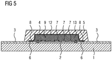
- Fig. 5 shows a control unit as in Fig. 3
- an opening 12 is arranged in the housing cover 4, through which a protective gel 13 has been introduced into the cavity 9 before the polymer 5 is encapsulated, which usually covers at least the electronic components 7 on the connecting device 2.
- the entire cavity 9 is encapsulated with the protective gel 13.
- the opening 12 of the housing cover 4 is secured by means of an adhesive, a spherical one Closure device or a polymer material has been tightly closed.
- the protective gel 13 means additional protection for the electronics in the control unit.
Landscapes
- Engineering & Computer Science (AREA)
- Microelectronics & Electronic Packaging (AREA)
- Manufacturing & Machinery (AREA)
- Casings For Electric Apparatus (AREA)
- Connection Or Junction Boxes (AREA)
Description
- Die Erfindung betrifft ein Steuergerät für ein Kraftfahrzeug und ein Verfahren zu dessen Herstellung nach dem Oberbegriff der unabhängigen Ansprüche.
- In der Kraftfahrzeugtechnik werden Komponenten wie Getriebe-, Motoren- oder Bremssysteme zunehmend vornehmlich elektronisch gesteuert. Hierbei gibt es eine Entwicklung hin zu integrierten mechatronischen Steuerungen, also zur Integration von Steuerelektronik und den zugehörigen elektronischen Komponenten wie Sensoren oder Ventile in das Getriebe, den Motor oder das Bremssystem. Steuergeräte weisen also im Allgemeinen eine Vielzahl an elektronischen Komponenten auf, welche in Verbindung mit anderen Komponenten außerhalb des Steuergerätes stehen. Bei solchen "Vorort-Elektroniken" sind diese Steuerungen nicht mehr in einem separaten geschützten Elektronikraum untergebracht und müssen daher entsprechenden Umwelteinflüssen und mechanischen, thermischen sowie chemischen Beanspruchungen standhalten. Sie werden zu diesem Zweck normalerweise in spezielle Gehäuse eingesetzt.
- Um eine verlässliche Verbindung zu außerhalb des Gehäuses liegenden Komponenten zu ermöglichen, ist eine elektrische Verbindung von der Gehäuseinnenseite zur Gehäuseaußenseite notwendig.
- Die Schaltungsträger für derartige Steuerungen werden in der Regel aufgebaut, in ein Gehäuse eingebracht und anschließend wird dieses Gehäuse verschlossen. Ein Beispiel hierfür wird in der
DE 10 2007 038 331 A1 beschrieben. Dieser Gehäuseaufbau garantiert jedoch keine absolute Dichtheit gegen Diffusion bzw. Permeation. Schadgase können im Laufe der Zeit zu dem Schaltungsträger gelangen und zu Metallkorrosion führen. - Bei einem alternativen Konzept wird der komplette Schaltungsaufbau zum Schutz des Schaltungsträgers vollständig mit Moldmasse umgossen. Ein Beispiel hierfür wird in der
DE 10 2011 082 537 A1 beschrieben. Die Prozessführung des Moldprozesses muss dabei genau eingehalten werden. Ansonsten kann es bei der Verwendung von ungehäusten elektronischen Bauteilen, sogenannten Bare Dies, die mittels Gold-Draht-Verbindungen mit dem Schaltungsträger elektrisch verbunden sind, zu sogenannten Bonddrahtverwehungen kommen. Ferner muss der thermische Ausdehnungskoeffizient des Moldmaterials genau an den des Gesamtaufbaus, bestehend aus Trägersubstrat, Bauteile usw. angepasst sein. Ansonsten kann es bei Temperaturbelastungen zu Spaltbildung zwischen Moldmasse und Aufbau kommen. - Eine weitere Möglichkeit des Abdichtens des Schaltungsraumes ist das Verschweißen des Gehäuses mit einem Edelstahldeckel. Dieses Verfahren ist vergleichsweise kostenintensiv und die elektrischen Anschlüsse müssen insbesondere über Glasdurchführungen vom Schaltungsträger durch das Edelstahlgehäuse nach außen geführt werden. Hier kann es leicht zu Fehlern im Prozess kommen. Des Weiteren können Gase, die durch den Schweißprozess im Gehäuseinneren entstehen, nur schwer wieder abgeführt werden.
- Die
DE102012215230A1 beschreibt ein Elektronikmodul mit Deckel und anspritzbarem Kunststoff-Dichtricht, insbesondere für ein Kfz-Steuergerät, wobei über den Kunststoff-Dichtring eine formschlüssige Verbindung zwischen dem Deckel und einem Leiterplattenelement bereitgestellt wird. - Aus der
DE102010062653A1 ist Steuermodul und ein Verfahren zu dessen Herstellung bekannt. DieDE102012213917A1 bezieht sich auf eine Bauelementummantelung für ein Elektronikbauteil, wobei ein formschlüssige Verbindung zwischen dem Mantelelement und der Leiterplatte bereitgestellt wird. - Der Erfindung liegt die Aufgabe zu Grunde, ein Steuergerät für ein Kraftfahrzeug zu schaffen, das einen vollständigen Schutz von Schaltung und Schaltungsträger gegen Schadgase und gegen aggressive Medien wie Getriebeöl bietet und gleichzeitig im Vergleich zu bisher bekannten Steuergeräten zu einer Reduzierung der Herstellungskosten führt.
- Diese Aufgabe wird erfindungsgemäß gelöst durch ein Steuergerät mit den Merkmalen des Anspruchs 1.
- Erfindungsgemäß wird ein Steuergerät beschrieben, das einen Gehäusedeckel mit einem umlaufenden, insbesondere planen, Randbereich und eine flächige, elektrische Verbindungsvorrichtung mit integrierten Leiterbahnen umfasst, wobei der Gehäusedeckel im Randbereich mit der Verbindungsvorrichtung unter Bildung einer Verbindungsnaht zumindest abschnittsweise stoffschlüssig verbunden ist und mit der Verbindungsvorrichtung einen Hohlraum einschließt. Die stoffschlüssige Verbindung zwischen dem Gehäusedeckel und der Verbindungsvorrichtung ist insbesondere mittels Kleben, Laminieren oder Löten hergestellt.
- Auf der Verbindungsvorrichtung ist mindestens ein elektronisches Bauteil innerhalb des Hohlraums angeordnet und die Verbindungsvorrichtung verbindet dieses elektronische Bauteil mit elektronischen Bauteilen außerhalb des Hohlraums elektrisch. Der Gehäusedeckel ist dabei auf seiner gesamten Oberfläche und über den umlaufenden Randbereich hinaus mit einem Polymer mediendicht umspritzt, wobei der Gehäusedeckel bevorzugt aus Kunststoff oder aus Metall ist und das Polymer vorwiegend als Moldmaterial, als Kleber oder als Harz ausgeführt ist.
- Die elektronischen Bauteile umfassen beispielsweise Kondensatoren, Spulen oder einen Mikroprozessor. In der Regel sind die elektronischen Bauteile über Leiterbahnen der Verbindungsvorrichtung und/oder mittels gebondeter Golddrähte miteinander elektrisch verbunden.
- Der Gehäusedeckel schützt die elektronischen Bauteile im Inneren des Steuergerätgehäuses vor Ölen, insbesondere aggressiven Ölen, sowie schädlichen Gasen und Chemikalien. Weiterhin sind die elektronischen Bauteile vor Salzen oder Verarbeitungsrückständen geschützt. Die Öle, Gase, Salze und/oder Rückstände liegen beispielsweise in einem Getriebe vor, an welchem oder innerhalb welchem das Steuergerät angeordnet ist. Auch die entsprechenden Leiterbahnen werden von dem Gehäusedeckel geschützt. Hierzu ist der Deckel, wie bereits erwähnt, im Randbereich stoffschlüssig mit der Verbindungsvorrichtung so verbunden, dass mit der Verbindungsvorrichtung ein abgeschlossener Hohlraum um die elektronischen Bauteile gebildet wird. Zusätzlich ist der Gehäusedeckel dabei über den umlaufenden Randbereich hinaus insbesondere komplett mit einem Polymer mediendicht umspritzt. Vorteilhafterweise kann dadurch auch ein Gehäusedeckel aus nicht mediendichtem Material, der damit in der Regel auch kostengünstiger ist, verwendet werden. Somit ist der Steuergerätaufbau gegen die Umgebung hermetisch abgedichtet.
- Im Gegensatz zu formschlüssig verbundenen Deckeln können insbesondere im Bereich der Verbindungsnaht keine Fluide und/oder Gase in den Hohlraum eintreten. Somit sind die elektronischen Komponenten versiegelt und gegen die Umwelt abgedichtet. Zusätzlich kann auf gummiartige Dichtungen verzichtet werden, welche insbesondere bei formschlüssig angebundenen Deckeln verwendet werden. Diese Dichtungen würden keine vollständige Gasdichtigkeit garantieren, da die Gase im Laufe der Zeit durch derartige Dichtungen in erheblichem Maße diffundieren können.
- Insbesondere umfassen die Chemikalien beziehungsweise Gase Schwefelverbindungen, wodurch Sulfide entstehen können. Sulfide sind zumindest teilweise stromleitend und würden sich an ungeschützten elektronischen Komponenten, den Leiterbahnen der Verbindungsvorrichtung und/oder den Golddrähten ablagern. Dabei kann es zu chemischen Reaktionen mit den Sulfiden kommen. Beispielsweise oxidieren die Leiterbahnen der Verbindungsvorrichtung, insbesondere Silberleiterbahnen, mit den Schwefelverbindungen. Dabei können sich Leitungswider-stände und/oder Funktionen der elektronischen Komponenten verändern und beispielsweise das Schaltverhalten eines Getriebes negativ beeinflussen. Weiterhin können derartige Gase Signalveränderungen bewirken, sodass es beispielsweise zu fehlerhaften Auswertungen durch die Steuergerätevorrichtung kommt.
- Insgesamt werden somit mittels des beschriebenen Aufbaus die Lebensdauer und die Genauigkeit des Steuergeräts verbessert. Weiter ist das beschriebene Steuergerät als vorgefertigtes Modul für eine Anwendung vorort wie beispielsweise im Getriebe oder als Anbausteuergerät realisierbar.
- Gemäß einer weiteren Ausgestaltung ist die Verbindungsvorrichtung als Leiterplatte mit mindestens einer Lage ausgeführt. Die Leiterplatte ist beispielsweise eine faserverstärkte Kunststoff- oder eine Keramikleiterplatte. Es könnte aber auch eine sogenannte HDI-Leiterplatte (High-Density-Interconnect) verwendet werden, welche sehr kompakt ausgestaltet ist. Die durchgehende Leiterplatte ragt hier über den gesamten umlaufenden Randbereich des Gehäusedeckels hinaus und bildet gleichzeitig den Boden des Gehäuses. Dadurch wird insbesondere ein flacher Aufbau des Steuergerätes erreicht.
- Um eine zusätzliche Versteifung dieses Aufbaus zu erreichen bzw. eine unter Umständen auftretende Verwölbung des Aufbaus im Bereich der Leiterplatte auszugleichen, kann der auf der dem Gehäusedeckel abgewandten Seite der Leiterplatte in dem der Verbindungsnaht entsprechenden Bereich zusätzlich Polymer aufgespritzt sein.
- Um den Niveauunterschied zwischen dem Randbereich des Deckels und der Leiterplatte im Bereich der Umspritzung zu vermindern bzw. zu egalisieren, verläuft der umlaufende Randbereich des Gehäusedeckels vorteilhafter Weise in einer entsprechenden umlaufenden Nut in der Leiterplatte. Dadurch wird das Risiko einer Spaltbildung in der Umspritzung im Bereich der Verbindungsstelle reduziert.
- Gemäß einer weiteren Ausgestaltung ist die Verbindungsvorrichtung zum Teil als separater Schaltungsträger im Inneren des Hohlraums angeordnet, wobei auf dem separaten Schaltungsträger das mindestens eine elektronische Bauteil wie Kondensator, Spule oder Mikroprozessor angeordnet ist. Die elektronischen Bauteile sind insbesondere über Leiterbahnen des Schaltungsträgers und/oder mittels gebondeter Golddrähte miteinander elektrisch verbunden. Der separate Schaltungsträger ist beispielsweise eine faserverstärkte Kunststoff- oder eine Keramikleiterplatte mit je einer oder mehreren Lagen. Alternativ könnte aber auch eine sogenannte HDI-Leiterplatte (High-Density-Interconnect) verwendet werden, welche konstruktionsbedingt sehr kompakt ausgestaltet ist.
- Das mindestens eine elektronische Bauteil auf dem separaten Schaltungsträger ist bevorzugt mittels einer separaten Leiterplatte mit elektronischen Bauteilen außerhalb des Hohlraums elektrisch verbunden. Als separate Leiterplatte wird insbesondere eine flexible Leiterplatte, die ganzflächig, mit einer Aussparung zur Aufnahme des separaten Schaltungsträgers, oder streifenförmig ausgeführt ist, verwendet. Bei diesem Ausführungsbeispiel sind der separate Schaltungsträger und die separate Leiterplatte auf einer gemeinsamen, über den gesamten umlaufenden Randbereich des Gehäusedeckels hinaus ragenden Trägerplatte angeordnet. Hier wird der Hohlraum im Steuergerät im Wesentlichen durch den Gehäusedeckel und die Trägerplatte umschlossen. In der Regel ist die Trägerplatte wegen ihrer Anforderungen in Bezug auf Steifigkeit und Wärmeableitvermögen aus Metall, insbesondere aus Aluminium gefertigt. Wird als separate Leiterplatte eine Flexfolie verwendet, so ist diese bevorzugt auf die Trägerplatte auflaminiert. Wenn die flexible Leiterplatte vollflächig mit einer Aussparung zur Aufnahme des Schaltungsträgers ausgeführt ist, wird diese im Wesentlichen vom Randbereich des Gehäusedeckels vollständig umlaufend überdeckt. Wenn die flexible Leiterplatte streifenförmig ausgeführt ist, wird diese vom umlaufenden Randbereich des Gehäusedeckels naturgemäß nur abschnittsweise, in der Regel quer zu den Leiterbahnen überdeckt.
- In einer weiteren Ausgestaltung verläuft der umlaufende Randbereich des Gehäusedeckels vorteilhafter Weise in einer entsprechenden umlaufenden Nut in der Trägerplatte. Dadurch wird der Niveauunterschied zwischen dem Randbereich des Deckels und Trägerplatte im Bereich der Umspritzung verkleinert oder gar egalisiert und somit das Risiko einer Spaltbildung im Polymer im Bereich der Verbindungsnaht reduziert.
- Gemäß einer weiteren Ausgestaltung ist im Gehäusedeckel eine Öffnung angeordnet, durch die vor der Umspritzung ein Schutzgel in den Hohlraum eingebracht werden kann, das zumindest die elektronischen Bauelemente auf der Verbindungsvorrichtung bedeckt. Es wäre auch denkbar, den gesamten Hohlraum mit dem Schutzgel zu vergießen. Nach dem Einbringen des Schutzgels wird die Öffnung des Gehäusedeckels mittels eines Klebers, einer kugelartigen Verschlussvorrichtung oder eines Polymermaterials dicht verschlossen. Das Schutzgel bedeutet einen zusätzlichen Schutz der Elektronik in dem Steuergerät.
- Eine weitere Aufgabe der Erfindung ist es, ein Verfahren zum Herstellen des erfindungsgemäßen Steuergerätes zu schaffen. Diese Aufgabe wird erfindungsgemäß gelöst durch ein Verfahren mit den Merkmalen des Anspruchs 15.
- Das Verfahren umfasst die Schritte:
- Bereitstellen der Verbindungsvorrichtung, auf welcher die elektronischen Bauteile angeordnet sind,
- Bereitstellen des Gehäusedeckels,
- stoffschlüssiges Verbinden des Gehäusedeckels mit der Verbindungsvorrichtung derart, dass dieser mit der Verbindungsvorrichtung einen abgeschlossenen Hohlraum bildet, in welchem sich die elektronischen Bauteile befinden,
- Umspritzen des Gehäusedeckels mit einem Polymer derart, dass das umspritzte Polymer über den umlaufenden Randbereich des Gehäusedeckels hinausreicht.
- In einer weiteren Ausgestaltung des Verfahrens wird vor dem Umspritzen des Gehäusedeckels mit einem Polymer durch eine Öffnung im Gehäusedeckel insbesondere ein Schutzgel in den Hohlraum eingebracht, das mindestens die elektronischen Bauelemente auf der Verbindungsvorrichtung bedeckt. Es wäre auch möglich, den gesamten Hohlraum mit dem Schutzgel zu vergießen. Nach dem Einbringen des Schutzgels wird die Öffnung des Gehäusedeckels mittels eines Klebers, einer kugelartigen Verschlussvorrichtung oder eines Polymermaterials dicht verschlossen.
- Weitere Merkmale, Vorteile und Einzelheiten sind der nachfolgenden Beschreibung entnehmbar, in der bevorzugte Ausführungsbeispiele näher erläutert werden. Es zeigen:
- Fig. 1
- einen Schnitt durch ein Steuergerät mit einer durchgehenden Leiterplatte als Verbindungsvorrichtung,
- Fig. 2
- ein Steuergerät wie in der
Figur 1 , mit beidseitig aufgebrachtem Polymer, - Fig. 3
- einen Schnitt durch ein Steuergerät mit einem separaten Schaltungsträger und einer separaten Leiterplatte,
- Fig. 4
- ein Steuergerät wie in der
Figur 3 , jedoch mit einer Nut in der Trägerplatte, und - Fig. 5
- ein Steuergerät wie in der
Figur 3 , jedoch mit Schutzgel im Hohlraum. -
Figuren 1 und 2 , bzw. 3 bis 5 zeigen schematische Schnittansichten eines Steuergerätes gemäß zweier unterschiedlicher Ausführungsprinzipien, wobeiFig. 1 und Fig. 2 das erste undFig. 3 bis 5 das zweite Ausführungsprinzip wiedergeben. Zunächst werden Gemeinsamkeiten der zwei Ausführungsprinzipien beschrieben, ehe auf die Unterschiede eingegangen wird. - Bei den Ausführungsbeispielen handelt es sich um ein Steuergerät eines Automatikgetriebes eines Kraftfahrzeuges. Das Steuergerät vermag beispielsweise Messwerte von Sensoren wie Hall-Sensoren auszuwerten und eine Schaltung des Automatikgetriebes in Abhängigkeit der Messwerte zu steuern. Alternativ kann das Steuergerät auch für andere Einsatzzwecke wie zum Beispiel in einem Motor eines Kraftfahrzeuges vorgesehen sein.
- Jedes Steuergerät weist eine Verbindungsvorrichtung 2, 3 auf. Auf der Verbindungsvorrichtung 2, 3 ist eine Mehrzahl von elektronischen Bauteilen 7 angeordnet. Diese umfassen beispielsweise Kondensatoren, Spulen, wenigstens einen Mikroprozessor und/oder andere Komponenten. Die elektronischen Bauteile 7 sind miteinander elektrisch verbunden, insbesondere über gebondete Golddrähte und/oder Leiterbahnen der Verbindungsvorrichtung 2, 3.
- Zum Schutz der elektronischen Bauteile 7 und der entsprechenden Leiterbahnen ist ein Gehäusedeckel 4 in seinem umlaufenden Randbereich 8 mit der Verbindungsvorrichtung 2, 3 unter Ausbildung einer umlaufenden Verbindungsnaht 6 stoffschlüssig verbunden. Die stoffschlüssige Verbindung zwischen dem Gehäusedeckel 4 und der Verbindungsvorrichtung 2, 3 ist mittels Kleben hergestellt. Diese Verbindung kann aber auch zum Beispiel durch Laminieren oder Löten realisiert sein. Der Gehäusedeckel 4 ist wahlweise aus Metall oder Kunststoff gefertigt.
- Der Gehäusedeckel 4 umschließt mit der Verbindungsvorrichtung 2, 3 einen abgeschlossenen Hohlraum 9. Somit ist die stoffschlüssige Verbindungsnaht 6 zusammenhängend zwischen dem Gehäusedeckel 4 und der Verbindungsvorrichtung 2, 3 um die elektronischen Bauteile 7 ausgebildet.
- Die Verbindungsvorrichtung 2, 3 verbindet die elektronischen Bauteile 7 im Inneren des Steuergeräts mit hier nicht gezeigten elektronischen Bauteilen außerhalb des Hohlraums 9 bzw. Steuergeräts elektrisch.
- Der Gehäusedeckel 4 ist komplett und über seinen umlaufenden Randbereich 8 hinaus mit einem Polymer 5 mediendicht umspritzt. Dadurch kann auch ein Gehäusedeckel 4 aus nicht mediendichtem Material, der damit in der Regel auch kostengünstiger ist, verwendet werden.
- Der umlaufende Randbereich 8 des Gehäusedeckels 4 ist dabei mindestens im Bereich der Verbindungsnaht 6 zwischen dem Gehäusedeckel 4 und der Verbindungsvorrichtung 2, 3 mit einem Polymer 5 insbesondere derart umspritzt, dass sich das Polymer 5 in der vom Gehäusedeckel 4 abgewandten Richtung über den Randbereich 8 hinaus über die Verbindungsvorrichtung 2, 3 beispielsweise zumindest der Breite des Randbereichs 8 nach erstreckt. Die Breite der Umspritzung hängt unter anderem von der Art des verwendeten Polymers 5 und von der Oberflächenbeschaffenheit der umspritzten Flächen ab. Zum Beispiel können der Randbereich 8 und die Verbindungsvorrichtung 2,3 jeweils plan ausgeführt sein. Alternativ können der Randbereich 8 und die Verbindungsvorrichtung 2,3 je eine entsprechende Struktur aufweisen, die im zusammengefügten Zustand zu einer verbesserten Festigkeit und Dichtheit der Verbindung, vor allem über die Lebensdauer, erzeugen kann. Dadurch ist sichergestellt, dass der Bereich der Verbindungsnaht 6 zwischen dem Gehäusedeckel 4 und der Verbindungsvorrichtung 2, 3 ausreichend mit Polymermaterial 5 bedeckt ist, und somit der Steuergerätaufbau insbesondere in diesem Bereich gegen die Umgebung, beispielweise Öle, insbesondere aggressive Öle, sowie schädliche Gase und Chemikalien hermetisch abgedichtet ist. Das Polymer 5 ist als Moldmaterial, alternativ dazu als Kleber oder als Harz ausgeführt.
- Im Folgenden werden die Unterschiede der zwei Ausführungsprinzipien gemäß den
Figuren 1 bis 5 erläutert. - Im Ausführungsbeispiel gemäß
Figur 1 ist die Verbindungsvorrichtung als Leiterplatte 2 mit mindestens einer Lage ausgeführt. Die Leiterplatte 2 ist beispielsweise eine faserverstärkte Kunststoff-, eine Keramikleiterplatte oder eine HDI-Leiterplatte. Die durchgehende Leiterplatte 2 ragt hier über den gesamten umlaufenden Randbereich 8 des Gehäusedeckels 4 hinaus und bildet gleichzeitig den Boden des Steuergerätgehäuses. Dadurch wird insbesondere ein flacher Aufbau des Steuergerätes erreicht. - Um eine zusätzliche Versteifung des Steuergeräteaufbaus zu erreichen bzw. um eine unter Umständen auftretende Verwölbung des Aufbaus im Bereich der Leiterplatte 2 auszugleichen, kann, wie in
Fig. 2 gezeigt, auf der dem Gehäusedeckel 4 abgewandten Seite der Leiterplatte 2 in dem der Verbindungsnaht 6 entsprechenden Bereich 10 zusätzlich Polymer 5 aufgespritzt sein. - Im Ausführungsbeispiel gemäß
Figur 3 umfasst die Verbindungsvorrichtung 2, 3 einen separaten Schaltungsträger 2, auf dem alle elektronischen Bauteile 7 angeordnet sind, und eine separate Leiterplatte 3 mittels der die elektronischen Bauteile 7 im Inneren des Steuergerätes mit nicht gezeigten elektronischen Bauteilen außerhalb des Steuergerätes elektrisch verbunden sind. Der separate Schaltungsträger 2 und die separate Leiterplatte 3 sind hier mittels Bonddrähten verbunden. Der separate Schaltungsträger 2 und die separate Leiterplatte 3 sind auf einer gemeinsamen, über den gesamten umlaufenden Randbereich 8 des Gehäusedeckels 4 hinaus ragenden Trägerplatte 1 angeordnet. Hier wird der Hohlraum 9 im Wesentlichen durch den Gehäusedeckel 4 und die Trägerplatte 1 umschlossen. - Der separate Schaltungsträger 2 ist als eine faserverstärkte Kunststoffleiterplatte oder alternativ als eine Keramikleiterplatte oder HDI-Leiterplatte mit jeweils einer oder mehreren Lagen ausgeführt. Es können jedoch auch andere Ausgestaltungsformen eines Schaltungsträgers Verwendung finden. Die elektronischen Bauteile 7 sind miteinander elektrisch verbunden, insbesondere über gebondete Golddrähte und/oder Leiterbahnen des separaten Schaltungsträgers 2.
- Als separate Leiterplatte 3 wird bevorzugt eine flexible Leiterplatte aus Polyimid verwendet. Diese flexible Leiterplatte 3 ist entweder als geschlossenen Fläche, mit einer Aussparung zur Aufnahme des Schaltungsträgers 2, oder streifenförmig ausgeführt.
- Üblicherweise ist die Trägerplatte wegen ihrer Anforderungen in Bezug auf Steifigkeit und Wärmeableitvermögen aus Metall, insbesondere aus Aluminium gefertigt. Der separate Schaltungsträger 2 und die separate Leiterplatte 3 sind auf die Trägerplatte 1 üblicherweise geklebt oder laminiert. Wenn die flexible Leiterplatte 3 ganzflächig ausgeführt ist, wird diese im Wesentlichen vom Randbereich 8 des Gehäusedeckels 4 vollständig umlaufend überdeckt.
- Falls die flexible Leiterplatte 3 streifenförmig ausgeführt ist, wird diese vom umlaufenden Randbereich 8 des Gehäusedeckels 4 konstruktionsbedingt nur abschnittsweise, in der Regel quer zu den Leiterbahnen der Leiterplatte 3 überdeckt. Die Verbindungsnaht 6 erstreckt sich somit auf der einen Seite über den umlaufenden Randbereich 8 und auf der anderen Seite über die Streifen der Leiterplatte 3 bzw. die Trägerplatte 1.
-
Fig. 4 zeigt ein Steuergerät wie inFig. 3 , jedoch verläuft der umlaufende Randbereich 8 des Gehäusedeckels 4 in einer entsprechenden umlaufenden Nut 11 in der Trägerplatte 1. Dadurch wird der Niveauunterschied zwischen dem Randbereich 8 und der Trägerplatte 1 im Bereich der Umspritzung 5 verkleinert bzw. egalisiert und somit das Risiko einer Spaltbildung im Polymer 5 im Bereich der Verbindungsnaht 6 reduziert. - Eine derartige Nut wäre auch im ersten Ausführungsprinzip gemäß den
Figuren 1 und 2 entsprechend in der Leiterplatte 2 denkbar. -
Fig. 5 zeigt ein Steuergerät wie inFig. 3 , jedoch ist im Gehäusedeckel 4 eine Öffnung 12 angeordnet, durch die vor der Umspritzung mit Polymer 5 ein Schutzgel 13 in den Hohlraum 9 eingebracht worden ist, das in der Regel zumindest die elektronischen Bauelemente 7 auf der Verbindungsvorrichtung 2 bedeckt. Hier ist der gesamte Hohlraum 9 mit dem Schutzgel 13 vergossen. Nach dem Einbringen des Schutzgels 13 ist die Öffnung 12 des Gehäusedeckels 4 mittels eines Klebers, einer kugelartigen Verschlussvorrichtung oder eines Polymermaterials dicht verschlossen worden. Das Schutzgel 13 bedeutet einen zusätzlichen Schutz der Elektronik in dem Steuergerät. - Ein derartiges Einbringen eines Schutzgels 13 wäre auch im ersten Ausführungsprinzip gemäß den
Figuren 1 und 2 denkbar. -
- 1
- Trägerplatte
- 2
- Verbindungsvorrichtung, separater Schaltungsträger
- 3
- Verbindungsvorrichtung, separate Leiterplatte
- 4
- Gehäusedeckel
- 5
- Polymer
- 6
- Verbindungsnaht
- 7
- Bauteil
- 8
- umlaufenden Randbereich des Gehäusedeckels 4
- 9
- Hohlraum
- 10
- Bereich
- 11
- Nut
- 12
- Öffnung im Gehäusedeckel 4
- 13
- Schutzgel
Claims (16)
- Steuergerät in einem Kraftfahrzeug, umfassenda) einen Gehäusedeckel (4) mit einem umlaufenden Randbereich (8) ,b) eine flächige, elektrische Verbindungsvorrichtung (2, 3) mit integrierten Leiterbahnen, wobei der Gehäusedeckel (4) im Randbereich (8) zumindest mit der Verbindungsvorrichtung (2, 3) unter Ausbildung einer Verbindungsnaht (6) stoffschlüssig verbunden ist und mit der Verbindungsvorrichtung (2, 3) einen Hohlraum (9) bildet,c) mindestens ein elektronisches Bauteil (7) innerhalb des Hohlraums (9), wobei die Verbindungsvorrichtung (2, 3) das mindestens eine elektronische Bauteil (7) mit elektronischen Bauteilen außerhalb des Hohlraums (9) elektrisch verbindet,wobei
der Gehäusedeckel (4) über den umlaufenden Randbereich (8) hinaus mit einem Polymer (5) mediendicht umspritzt ist. - Steuergerät nach Anspruch 1, dadurch gekennzeichnet, dass die Verbindungsvorrichtung (2) als Leiterplatte mit mindestens einer Lage ausgeführt ist, wobei die Leiterplatte (2) über den gesamten umlaufenden Randbereich (8) des Gehäusedeckels (4) hinausragt.
- Steuergerät nach Anspruch 2, dadurch gekennzeichnet, dass auf der dem Gehäusedeckel (4) abgewandten Seite der Leiterplatte (2) in dem der Verbindungsnaht (6) entsprechenden Bereich (10) zusätzlich Polymer (5) aufgespritzt ist.
- Steuergerät nach Anspruch 2 oder 3, dadurch gekennzeichnet, dass der umlaufende Randbereich (8) des Gehäusedeckels (4) in einer umlaufenden Nut (11) in der Leiterplatte (2) verläuft.
- Steuergerät nach Anspruch 1, dadurch gekennzeichnet, dass die Verbindungsvorrichtung (2, 3) als separater Schaltungsträger (2) im Inneren des Hohlraums (9) ausgeführt ist, wobei auf dem separaten Schaltungsträger (2) das mindestens eine elektronische Bauteil (7) angeordnet ist, welches mittels einer separaten Leiterplatte (3) mit elektronischen Bauteilen außerhalb des Hohlraums (9) elektrisch verbunden ist, und wobei der separate Schaltungsträger (2) und die separate Leiterplatte (3) auf einer gemeinsamen, über den gesamten umlaufenden Randbereich (8) des Gehäusedeckels (4) hinausragenden Trägerplatte (1) angeordnet sind.
- Steuergerät nach Anspruch 5, dadurch gekennzeichnet, dass die separate Leiterplatte (3) als flexible Leiterplatte ausgeführt ist
- Steuergerät nach Anspruch 5 oder 6, dadurch gekennzeichnet, dass die separate Leiterplatte (3) zumindest abschnittsweise von dem umlaufenden Randbereich (8) überdeckt ist.
- Steuergerät nach einem der Ansprüche 5 bis 7, dadurch gekennzeichnet, dass die Trägerplatte (1) aus Metall, zum Beispiel Aluminium ist.
- Steuergerät nach einem der Ansprüche 5 bis 8, dadurch gekennzeichnet, dass der umlaufende Randbereich (8) des Gehäusedeckels (4) in einer umlaufenden Nut (11) in der Trägerplatte (1) verläuft.
- Steuergerät nach einem der vorhergehenden Ansprüche, dadurch gekennzeichnet, dass das Polymer als Moldmaterial, als Kleber oder als Harz ausgeführt ist.
- Steuergerät nach einem der vorhergehenden Ansprüche, dadurch gekennzeichnet, dass der Gehäusedeckel (4) aus Kunststoff oder aus Metall ist.
- Steuergerät nach einem der vorhergehenden Ansprüche, dadurch gekennzeichnet, dass die stoffschlüssige Verbindung zwischen Gehäusedeckel (4) und der Verbindungsvorrichtung (2, 3) mittels Kleben, Laminieren oder Löten hergestellt ist.
- Steuergerät nach einem der vorhergehenden Ansprüche, dadurch gekennzeichnet, dass im Gehäusedeckel (4) eine Öffnung (12) angeordnet ist, durch die ein Schutzgel (13) in den Hohlraum (9) eingebracht ist, das zumindest die elektronischen Bauelemente (7) auf der Verbindungsvorrichtung (2, 3) bedeckt.
- Steuergerät nach Anspruch 13, dadurch gekennzeichnet, dass die Öffnung (12) mittels eines Klebers, einer kugelartigen Verschlussvorrichtung oder Polymermaterial (5) verschlossen ist.
- Verfahren zum Herstellen einer Steuergerätevorrichtung nach einem der Ansprüche 1 bis 14, umfassend die Schritte- Bereitstellen der Verbindungsvorrichtung (2, 3), auf welcher die elektronischen Bauteile (7) angeordnet sind,- Bereitstellen des Gehäusedeckels (4);- stoffschlüssiges Verbinden des Gehäusedeckels (4) mit der Verbindungsvorrichtung (2, 3) derart, dass dieser mit der Verbindungsvorrichtung (2, 3) einen abgeschlossenen Hohlraum (5) bildet, in welchem sich die elektronischen Bauteile (7) befinden,- Umspritzen des Gehäusedeckels (4) mit einem Polymer derart, dass das umspritzte Polymer über den umlaufenden Randbereich (8) des Gehäusedeckels (4) hinaus reicht.
- Verfahren nach Anspruch 15, wobei vor dem Umspritzen des Gehäusedeckels (4) durch eine Öffnung (12) im Gehäusedeckel (4) ein Schutzgel (13) in den Hohlraum (9) eingebracht wird, das mindestens die elektronischen Bauelemente (7) auf der Verbindungsvorrichtung (2, 3) bedeckt, und wobei anschließend die Öffnung (12) dicht verschlossen wird.
Applications Claiming Priority (2)
| Application Number | Priority Date | Filing Date | Title |
|---|---|---|---|
| DE102015217576.6A DE102015217576B4 (de) | 2015-09-15 | 2015-09-15 | Mediendichtes Steuergerät für ein Kraftfahrzeug und Verfahren zur Herstellung des Steuergerätes |
| PCT/EP2016/069397 WO2017045854A1 (de) | 2015-09-15 | 2016-08-16 | Mediendichtes steuergerät für ein kraftfahrzeug und verfahren zur herstellung des steuergerätes |
Publications (2)
| Publication Number | Publication Date |
|---|---|
| EP3351068A1 EP3351068A1 (de) | 2018-07-25 |
| EP3351068B1 true EP3351068B1 (de) | 2021-10-13 |
Family
ID=56851549
Family Applications (1)
| Application Number | Title | Priority Date | Filing Date |
|---|---|---|---|
| EP16758106.5A Active EP3351068B1 (de) | 2015-09-15 | 2016-08-16 | Mediendichtes steuergerät für ein kraftfahrzeug und verfahren zur herstellung des steuergerätes |
Country Status (6)
| Country | Link |
|---|---|
| US (1) | US10506732B2 (de) |
| EP (1) | EP3351068B1 (de) |
| JP (1) | JP6611920B2 (de) |
| CN (1) | CN108029208B (de) |
| DE (1) | DE102015217576B4 (de) |
| WO (1) | WO2017045854A1 (de) |
Families Citing this family (9)
| Publication number | Priority date | Publication date | Assignee | Title |
|---|---|---|---|---|
| DE102015217572B3 (de) | 2015-09-15 | 2017-03-16 | Conti Temic Microelectronic Gmbh | Mediendichtes Steuergerät für ein Kraftfahrzeug |
| DE102016224352B4 (de) | 2016-12-07 | 2024-01-25 | Vitesco Technologies Germany Gmbh | Gehäuse zur Aufnahme von elektronischen Komponenten |
| DE102018215711A1 (de) * | 2018-09-14 | 2020-03-19 | Robert Bosch Gmbh | Steuergeräteeinheit und Verfahren zum Herstellen einer Steuergeräteeinheit |
| CN110213952A (zh) * | 2019-05-28 | 2019-09-06 | 青岛歌尔微电子研究院有限公司 | 一种电磁屏蔽结构及其制造方法及电子设备 |
| US11935799B2 (en) * | 2019-06-25 | 2024-03-19 | Intel Corporation | Integrated circuit package lids with polymer features |
| DE102019215659B4 (de) * | 2019-10-11 | 2021-08-12 | Continental Automotive Gmbh | Schaltungsbaugruppe |
| US10893604B1 (en) | 2020-03-03 | 2021-01-12 | Goodrich Corporation | Potted printed circuit board module and methods thereof |
| DE102020122428A1 (de) | 2020-08-27 | 2022-03-03 | Bayerische Motoren Werke Aktiengesellschaft | Metall-Kunststoff-Hybridgehäuse sowie Verfahren zur Herstellung eines Metall-Kunststoff-Hybridgehäuses |
| DE102021202853B4 (de) | 2021-03-24 | 2022-10-06 | Vitesco Technologies Germany Gmbh | Elektronische Baugruppe mit verbessertem Sicherungskonzept |
Family Cites Families (16)
| Publication number | Priority date | Publication date | Assignee | Title |
|---|---|---|---|---|
| JPS52117396A (en) | 1976-03-29 | 1977-10-01 | Kuraray Co Ltd | Preparation of polyesters with improved whiteness |
| JPS5441953U (de) * | 1977-08-31 | 1979-03-20 | ||
| JPS6017301B2 (ja) | 1977-09-09 | 1985-05-02 | 鐘淵化学工業株式会社 | 強化ポリ塩化ビニル系樹脂成形材料 |
| JP2907914B2 (ja) * | 1989-01-16 | 1999-06-21 | シーメンス、アクチエンゲゼルシヤフト | 電気又は電子デバイス又はモジユールの封止方法とパツケージ |
| US7109410B2 (en) * | 2003-04-15 | 2006-09-19 | Wavezero, Inc. | EMI shielding for electronic component packaging |
| DE10355282A1 (de) * | 2003-11-18 | 2005-06-16 | E.G.O. Elektro-Gerätebau GmbH | Verfahren zur Herstellung einer Übertemperatursicherung und Übertemperatursicherung |
| WO2005069462A1 (ja) * | 2004-01-13 | 2005-07-28 | Taisei Plas Co., Ltd. | ジャンクション用電装品とその製造方法 |
| DE102006050351A1 (de) * | 2006-10-25 | 2008-05-08 | Siemens Ag | Gehäuse für ein elektronisches Steuergerät |
| DE102007038331B4 (de) | 2007-08-14 | 2022-02-24 | Vitesco Technologies GmbH | Elektronisches Bauteil und Verfahren zur Herstellung eines elektronischen Bauteils |
| DE102009002519A1 (de) * | 2009-04-21 | 2010-10-28 | Robert Bosch Gmbh | Gekapselte Schaltungsvorrichtung für Substrate mit Absorptionsschicht sowie Verfahren zu Herstellung derselben |
| DE102010062653A1 (de) * | 2010-12-08 | 2012-06-14 | Robert Bosch Gmbh | Steuermodul und Verfahren zu seiner Herstellung |
| DE102011082537A1 (de) | 2011-09-12 | 2013-03-14 | Robert Bosch Gmbh | Leiterplatte und elektrische Bauteile zum Einsatz in aggressiver Umgebung und Verfahren zur Herstellung einer solchen Leiterplatte |
| DE102012213917A1 (de) * | 2012-08-06 | 2014-02-20 | Robert Bosch Gmbh | Bauelemente-Ummantelung für ein Elektronikmodul |
| DE102012108147A1 (de) * | 2012-09-03 | 2014-03-27 | Sick Ag | Sensoranordnung |
| DE102013215230A1 (de) * | 2013-08-02 | 2015-02-05 | Robert Bosch Gmbh | Elektronikmodul mit Deckel und anspritzbarem Kunststoff-Dichtring, insbesondere für ein Kfz-Getriebesteuergerät, und Verfahren zum Fertigen desselben |
| DE102015217572B3 (de) | 2015-09-15 | 2017-03-16 | Conti Temic Microelectronic Gmbh | Mediendichtes Steuergerät für ein Kraftfahrzeug |
-
2015
- 2015-09-15 DE DE102015217576.6A patent/DE102015217576B4/de not_active Expired - Fee Related
-
2016
- 2016-08-16 WO PCT/EP2016/069397 patent/WO2017045854A1/de active Application Filing
- 2016-08-16 CN CN201680050585.5A patent/CN108029208B/zh active Active
- 2016-08-16 JP JP2018513450A patent/JP6611920B2/ja active Active
- 2016-08-16 EP EP16758106.5A patent/EP3351068B1/de active Active
-
2018
- 2018-03-14 US US15/921,383 patent/US10506732B2/en active Active
Also Published As
| Publication number | Publication date |
|---|---|
| US10506732B2 (en) | 2019-12-10 |
| EP3351068A1 (de) | 2018-07-25 |
| CN108029208B (zh) | 2020-10-30 |
| US20180206355A1 (en) | 2018-07-19 |
| JP6611920B2 (ja) | 2019-11-27 |
| JP2018530295A (ja) | 2018-10-11 |
| DE102015217576A1 (de) | 2017-03-16 |
| DE102015217576B4 (de) | 2017-03-30 |
| CN108029208A (zh) | 2018-05-11 |
| WO2017045854A1 (de) | 2017-03-23 |
Similar Documents
| Publication | Publication Date | Title |
|---|---|---|
| EP3351068B1 (de) | Mediendichtes steuergerät für ein kraftfahrzeug und verfahren zur herstellung des steuergerätes | |
| EP3351067B1 (de) | Mediendichtes steuergerät für ein kraftfahrzeug | |
| EP2796016B1 (de) | Getriebesteuermodul | |
| EP3257339B1 (de) | Mechatronische komponente und verfahren zu deren herstellung | |
| EP3189716B1 (de) | Steuergerätevorrichtung für ein kraftfahrzeug sowie verfahren zum herstellen einer solchen | |
| EP2055154A1 (de) | Standardisiertes elektronikgehäuse mit modularen kontaktpartnern | |
| DE102013215227A1 (de) | Verkapseltes Elektronikmodul mit Flexfolienanbindung, insbesondere für ein Kfz-Getriebesteuermodul | |
| EP2055155B1 (de) | Steuergerät für ein kraftfahrzeug | |
| WO2008049724A1 (de) | Gehäuse für ein elektronisches steuergerät | |
| WO2011160897A1 (de) | Eingekapseltes steuerungsmodul für ein kraftfahrzeug | |
| EP1858312A2 (de) | Elektronische Baueinheit | |
| EP2033269B1 (de) | Elektronikgehäuse mit standardinterface | |
| WO2016177629A1 (de) | Elektronische komponente und verfahren zu deren herstellung | |
| DE102013215365A1 (de) | Elektrische Getriebesteuervorrichtung und Herstellungsverfahren | |
| EP3942259B1 (de) | Winkelerfassungseinrichtung | |
| DE102015224270B3 (de) | Elektronische Komponente und Verfahren zu deren Herstellung | |
| DE102015221161A1 (de) | Kontaktierungsanordnung, insbesondere für ein Getriebesteuermodul | |
| DE102015219011A1 (de) | Sensoranordnung für ein Getriebesteuergerät | |
| DE102017209058B4 (de) | Elektronische Schaltungsbaugruppe | |
| DE102016215072B4 (de) | Leiterplatte und Schaltungsbaugruppe mit einer Leiterplatte | |
| DE102019203827A1 (de) | Winkelerfassungseinrichtung | |
| WO2022223243A1 (de) | Verfahren zum verkapseln einer elektronischen baugruppe | |
| WO2008055751A2 (de) | Elektronikgehäuse mit neuer flexibler leiterplattentechnologie | |
| WO2017207141A1 (de) | Elektronikmodul für ein getriebesteuergerät mit auf fr4-leiterplattenfolie verklebtem deckel | |
| DE102016215407A1 (de) | Verfahren zur Herstellung einer elektronischen Schaltungsbaugruppe und elektronische Schaltungsbaugruppe |
Legal Events
| Date | Code | Title | Description |
|---|---|---|---|
| STAA | Information on the status of an ep patent application or granted ep patent |
Free format text: STATUS: THE INTERNATIONAL PUBLICATION HAS BEEN MADE |
|
| PUAI | Public reference made under article 153(3) epc to a published international application that has entered the european phase |
Free format text: ORIGINAL CODE: 0009012 |
|
| STAA | Information on the status of an ep patent application or granted ep patent |
Free format text: STATUS: REQUEST FOR EXAMINATION WAS MADE |
|
| 17P | Request for examination filed |
Effective date: 20180416 |
|
| AK | Designated contracting states |
Kind code of ref document: A1 Designated state(s): AL AT BE BG CH CY CZ DE DK EE ES FI FR GB GR HR HU IE IS IT LI LT LU LV MC MK MT NL NO PL PT RO RS SE SI SK SM TR |
|
| AX | Request for extension of the european patent |
Extension state: BA ME |
|
| RIN1 | Information on inventor provided before grant (corrected) |
Inventor name: WITTMANN, FRIEDER Inventor name: SCHUCH, BERNHARD Inventor name: BEART, KARIN Inventor name: BOCK, JOHANNES Inventor name: SCHMIDT, THOMAS |
|
| DAV | Request for validation of the european patent (deleted) | ||
| DAX | Request for extension of the european patent (deleted) | ||
| RAP1 | Party data changed (applicant data changed or rights of an application transferred) |
Owner name: VITESCO TECHNOLOGIES GERMANY GMBH |
|
| GRAP | Despatch of communication of intention to grant a patent |
Free format text: ORIGINAL CODE: EPIDOSNIGR1 |
|
| STAA | Information on the status of an ep patent application or granted ep patent |
Free format text: STATUS: GRANT OF PATENT IS INTENDED |
|
| INTG | Intention to grant announced |
Effective date: 20210511 |
|
| RIN1 | Information on inventor provided before grant (corrected) |
Inventor name: WITTMANN, FRIEDER Inventor name: BEART, KARIN Inventor name: BOCK, JOHANNES Inventor name: SCHMIDT, THOMAS Inventor name: SCHUCH, BERNHARD |
|
| GRAS | Grant fee paid |
Free format text: ORIGINAL CODE: EPIDOSNIGR3 |
|
| GRAA | (expected) grant |
Free format text: ORIGINAL CODE: 0009210 |
|
| STAA | Information on the status of an ep patent application or granted ep patent |
Free format text: STATUS: THE PATENT HAS BEEN GRANTED |
|
| AK | Designated contracting states |
Kind code of ref document: B1 Designated state(s): AL AT BE BG CH CY CZ DE DK EE ES FI FR GB GR HR HU IE IS IT LI LT LU LV MC MK MT NL NO PL PT RO RS SE SI SK SM TR |
|
| REG | Reference to a national code |
Ref country code: GB Ref legal event code: FG4D Free format text: NOT ENGLISH |
|
| REG | Reference to a national code |
Ref country code: CH Ref legal event code: EP |
|
| REG | Reference to a national code |
Ref country code: DE Ref legal event code: R081 Ref document number: 502016013997 Country of ref document: DE Owner name: VITESCO TECHNOLOGIES GERMANY GMBH, DE Free format text: FORMER OWNER: VITESCO TECHNOLOGIES GERMANY GMBH, 30165 HANNOVER, DE |
|
| REG | Reference to a national code |
Ref country code: DE Ref legal event code: R096 Ref document number: 502016013997 Country of ref document: DE |
|
| REG | Reference to a national code |
Ref country code: IE Ref legal event code: FG4D Free format text: LANGUAGE OF EP DOCUMENT: GERMAN |
|
| REG | Reference to a national code |
Ref country code: AT Ref legal event code: REF Ref document number: 1439131 Country of ref document: AT Kind code of ref document: T Effective date: 20211115 |
|
| RAP4 | Party data changed (patent owner data changed or rights of a patent transferred) |
Owner name: VITESCO TECHNOLOGIES GERMANY GMBH |
|
| REG | Reference to a national code |
Ref country code: LT Ref legal event code: MG9D |
|
| REG | Reference to a national code |
Ref country code: NL Ref legal event code: MP Effective date: 20211013 |
|
| PG25 | Lapsed in a contracting state [announced via postgrant information from national office to epo] |
Ref country code: RS Free format text: LAPSE BECAUSE OF FAILURE TO SUBMIT A TRANSLATION OF THE DESCRIPTION OR TO PAY THE FEE WITHIN THE PRESCRIBED TIME-LIMIT Effective date: 20211013 Ref country code: LT Free format text: LAPSE BECAUSE OF FAILURE TO SUBMIT A TRANSLATION OF THE DESCRIPTION OR TO PAY THE FEE WITHIN THE PRESCRIBED TIME-LIMIT Effective date: 20211013 Ref country code: FI Free format text: LAPSE BECAUSE OF FAILURE TO SUBMIT A TRANSLATION OF THE DESCRIPTION OR TO PAY THE FEE WITHIN THE PRESCRIBED TIME-LIMIT Effective date: 20211013 Ref country code: BG Free format text: LAPSE BECAUSE OF FAILURE TO SUBMIT A TRANSLATION OF THE DESCRIPTION OR TO PAY THE FEE WITHIN THE PRESCRIBED TIME-LIMIT Effective date: 20220113 |
|
| PG25 | Lapsed in a contracting state [announced via postgrant information from national office to epo] |
Ref country code: IS Free format text: LAPSE BECAUSE OF FAILURE TO SUBMIT A TRANSLATION OF THE DESCRIPTION OR TO PAY THE FEE WITHIN THE PRESCRIBED TIME-LIMIT Effective date: 20220213 Ref country code: SE Free format text: LAPSE BECAUSE OF FAILURE TO SUBMIT A TRANSLATION OF THE DESCRIPTION OR TO PAY THE FEE WITHIN THE PRESCRIBED TIME-LIMIT Effective date: 20211013 Ref country code: PT Free format text: LAPSE BECAUSE OF FAILURE TO SUBMIT A TRANSLATION OF THE DESCRIPTION OR TO PAY THE FEE WITHIN THE PRESCRIBED TIME-LIMIT Effective date: 20220214 Ref country code: PL Free format text: LAPSE BECAUSE OF FAILURE TO SUBMIT A TRANSLATION OF THE DESCRIPTION OR TO PAY THE FEE WITHIN THE PRESCRIBED TIME-LIMIT Effective date: 20211013 Ref country code: NO Free format text: LAPSE BECAUSE OF FAILURE TO SUBMIT A TRANSLATION OF THE DESCRIPTION OR TO PAY THE FEE WITHIN THE PRESCRIBED TIME-LIMIT Effective date: 20220113 Ref country code: NL Free format text: LAPSE BECAUSE OF FAILURE TO SUBMIT A TRANSLATION OF THE DESCRIPTION OR TO PAY THE FEE WITHIN THE PRESCRIBED TIME-LIMIT Effective date: 20211013 Ref country code: LV Free format text: LAPSE BECAUSE OF FAILURE TO SUBMIT A TRANSLATION OF THE DESCRIPTION OR TO PAY THE FEE WITHIN THE PRESCRIBED TIME-LIMIT Effective date: 20211013 Ref country code: HR Free format text: LAPSE BECAUSE OF FAILURE TO SUBMIT A TRANSLATION OF THE DESCRIPTION OR TO PAY THE FEE WITHIN THE PRESCRIBED TIME-LIMIT Effective date: 20211013 Ref country code: GR Free format text: LAPSE BECAUSE OF FAILURE TO SUBMIT A TRANSLATION OF THE DESCRIPTION OR TO PAY THE FEE WITHIN THE PRESCRIBED TIME-LIMIT Effective date: 20220114 Ref country code: ES Free format text: LAPSE BECAUSE OF FAILURE TO SUBMIT A TRANSLATION OF THE DESCRIPTION OR TO PAY THE FEE WITHIN THE PRESCRIBED TIME-LIMIT Effective date: 20211013 |
|
| REG | Reference to a national code |
Ref country code: DE Ref legal event code: R097 Ref document number: 502016013997 Country of ref document: DE |
|
| PG25 | Lapsed in a contracting state [announced via postgrant information from national office to epo] |
Ref country code: SM Free format text: LAPSE BECAUSE OF FAILURE TO SUBMIT A TRANSLATION OF THE DESCRIPTION OR TO PAY THE FEE WITHIN THE PRESCRIBED TIME-LIMIT Effective date: 20211013 Ref country code: SK Free format text: LAPSE BECAUSE OF FAILURE TO SUBMIT A TRANSLATION OF THE DESCRIPTION OR TO PAY THE FEE WITHIN THE PRESCRIBED TIME-LIMIT Effective date: 20211013 Ref country code: RO Free format text: LAPSE BECAUSE OF FAILURE TO SUBMIT A TRANSLATION OF THE DESCRIPTION OR TO PAY THE FEE WITHIN THE PRESCRIBED TIME-LIMIT Effective date: 20211013 Ref country code: EE Free format text: LAPSE BECAUSE OF FAILURE TO SUBMIT A TRANSLATION OF THE DESCRIPTION OR TO PAY THE FEE WITHIN THE PRESCRIBED TIME-LIMIT Effective date: 20211013 Ref country code: DK Free format text: LAPSE BECAUSE OF FAILURE TO SUBMIT A TRANSLATION OF THE DESCRIPTION OR TO PAY THE FEE WITHIN THE PRESCRIBED TIME-LIMIT Effective date: 20211013 Ref country code: CZ Free format text: LAPSE BECAUSE OF FAILURE TO SUBMIT A TRANSLATION OF THE DESCRIPTION OR TO PAY THE FEE WITHIN THE PRESCRIBED TIME-LIMIT Effective date: 20211013 |
|
| PLBE | No opposition filed within time limit |
Free format text: ORIGINAL CODE: 0009261 |
|
| STAA | Information on the status of an ep patent application or granted ep patent |
Free format text: STATUS: NO OPPOSITION FILED WITHIN TIME LIMIT |
|
| 26N | No opposition filed |
Effective date: 20220714 |
|
| PG25 | Lapsed in a contracting state [announced via postgrant information from national office to epo] |
Ref country code: AL Free format text: LAPSE BECAUSE OF FAILURE TO SUBMIT A TRANSLATION OF THE DESCRIPTION OR TO PAY THE FEE WITHIN THE PRESCRIBED TIME-LIMIT Effective date: 20211013 |
|
| PG25 | Lapsed in a contracting state [announced via postgrant information from national office to epo] |
Ref country code: SI Free format text: LAPSE BECAUSE OF FAILURE TO SUBMIT A TRANSLATION OF THE DESCRIPTION OR TO PAY THE FEE WITHIN THE PRESCRIBED TIME-LIMIT Effective date: 20211013 |
|
| PG25 | Lapsed in a contracting state [announced via postgrant information from national office to epo] |
Ref country code: MC Free format text: LAPSE BECAUSE OF FAILURE TO SUBMIT A TRANSLATION OF THE DESCRIPTION OR TO PAY THE FEE WITHIN THE PRESCRIBED TIME-LIMIT Effective date: 20211013 |
|
| REG | Reference to a national code |
Ref country code: CH Ref legal event code: PL |
|
| GBPC | Gb: european patent ceased through non-payment of renewal fee |
Effective date: 20220816 |
|
| PG25 | Lapsed in a contracting state [announced via postgrant information from national office to epo] |
Ref country code: LU Free format text: LAPSE BECAUSE OF NON-PAYMENT OF DUE FEES Effective date: 20220816 Ref country code: LI Free format text: LAPSE BECAUSE OF NON-PAYMENT OF DUE FEES Effective date: 20220831 Ref country code: CH Free format text: LAPSE BECAUSE OF NON-PAYMENT OF DUE FEES Effective date: 20220831 |
|
| REG | Reference to a national code |
Ref country code: BE Ref legal event code: MM Effective date: 20220831 |
|
| PG25 | Lapsed in a contracting state [announced via postgrant information from national office to epo] |
Ref country code: IT Free format text: LAPSE BECAUSE OF FAILURE TO SUBMIT A TRANSLATION OF THE DESCRIPTION OR TO PAY THE FEE WITHIN THE PRESCRIBED TIME-LIMIT Effective date: 20211013 |
|
| P01 | Opt-out of the competence of the unified patent court (upc) registered |
Effective date: 20230530 |
|
| PG25 | Lapsed in a contracting state [announced via postgrant information from national office to epo] |
Ref country code: IE Free format text: LAPSE BECAUSE OF NON-PAYMENT OF DUE FEES Effective date: 20220816 Ref country code: FR Free format text: LAPSE BECAUSE OF NON-PAYMENT OF DUE FEES Effective date: 20220831 |
|
| PG25 | Lapsed in a contracting state [announced via postgrant information from national office to epo] |
Ref country code: BE Free format text: LAPSE BECAUSE OF NON-PAYMENT OF DUE FEES Effective date: 20220831 |
|
| REG | Reference to a national code |
Ref country code: AT Ref legal event code: MM01 Ref document number: 1439131 Country of ref document: AT Kind code of ref document: T Effective date: 20220816 |
|
| PG25 | Lapsed in a contracting state [announced via postgrant information from national office to epo] |
Ref country code: GB Free format text: LAPSE BECAUSE OF NON-PAYMENT OF DUE FEES Effective date: 20220816 Ref country code: AT Free format text: LAPSE BECAUSE OF NON-PAYMENT OF DUE FEES Effective date: 20220816 |
|
| PGFP | Annual fee paid to national office [announced via postgrant information from national office to epo] |
Ref country code: DE Payment date: 20230831 Year of fee payment: 8 |
|
| PG25 | Lapsed in a contracting state [announced via postgrant information from national office to epo] |
Ref country code: HU Free format text: LAPSE BECAUSE OF FAILURE TO SUBMIT A TRANSLATION OF THE DESCRIPTION OR TO PAY THE FEE WITHIN THE PRESCRIBED TIME-LIMIT; INVALID AB INITIO Effective date: 20160816 |
|
| PG25 | Lapsed in a contracting state [announced via postgrant information from national office to epo] |
Ref country code: CY Free format text: LAPSE BECAUSE OF FAILURE TO SUBMIT A TRANSLATION OF THE DESCRIPTION OR TO PAY THE FEE WITHIN THE PRESCRIBED TIME-LIMIT Effective date: 20211013 |
|
| PG25 | Lapsed in a contracting state [announced via postgrant information from national office to epo] |
Ref country code: MK Free format text: LAPSE BECAUSE OF FAILURE TO SUBMIT A TRANSLATION OF THE DESCRIPTION OR TO PAY THE FEE WITHIN THE PRESCRIBED TIME-LIMIT Effective date: 20211013 |
|
| PG25 | Lapsed in a contracting state [announced via postgrant information from national office to epo] |
Ref country code: TR Free format text: LAPSE BECAUSE OF FAILURE TO SUBMIT A TRANSLATION OF THE DESCRIPTION OR TO PAY THE FEE WITHIN THE PRESCRIBED TIME-LIMIT Effective date: 20211013 |