EP3349249A2 - Parallelplattenwellenleiter für stromkreise - Google Patents
Parallelplattenwellenleiter für stromkreise Download PDFInfo
- Publication number
- EP3349249A2 EP3349249A2 EP17206878.5A EP17206878A EP3349249A2 EP 3349249 A2 EP3349249 A2 EP 3349249A2 EP 17206878 A EP17206878 A EP 17206878A EP 3349249 A2 EP3349249 A2 EP 3349249A2
- Authority
- EP
- European Patent Office
- Prior art keywords
- metal layer
- group
- strip
- substrate
- attached
- Prior art date
- Legal status (The legal status is an assumption and is not a legal conclusion. Google has not performed a legal analysis and makes no representation as to the accuracy of the status listed.)
- Granted
Links
Images







Classifications
-
- H—ELECTRICITY
- H10—SEMICONDUCTOR DEVICES; ELECTRIC SOLID-STATE DEVICES NOT OTHERWISE PROVIDED FOR
- H10W—GENERIC PACKAGES, INTERCONNECTIONS, CONNECTORS OR OTHER CONSTRUCTIONAL DETAILS OF DEVICES COVERED BY CLASS H10
- H10W20/00—Interconnections in chips, wafers or substrates
- H10W20/01—Manufacture or treatment
- H10W20/031—Manufacture or treatment of conductive parts of the interconnections
-
- H—ELECTRICITY
- H10—SEMICONDUCTOR DEVICES; ELECTRIC SOLID-STATE DEVICES NOT OTHERWISE PROVIDED FOR
- H10W—GENERIC PACKAGES, INTERCONNECTIONS, CONNECTORS OR OTHER CONSTRUCTIONAL DETAILS OF DEVICES COVERED BY CLASS H10
- H10W20/00—Interconnections in chips, wafers or substrates
- H10W20/01—Manufacture or treatment
- H10W20/031—Manufacture or treatment of conductive parts of the interconnections
- H10W20/056—Manufacture or treatment of conductive parts of the interconnections by filling conductive material into holes, grooves or trenches
-
- H—ELECTRICITY
- H10—SEMICONDUCTOR DEVICES; ELECTRIC SOLID-STATE DEVICES NOT OTHERWISE PROVIDED FOR
- H10W—GENERIC PACKAGES, INTERCONNECTIONS, CONNECTORS OR OTHER CONSTRUCTIONAL DETAILS OF DEVICES COVERED BY CLASS H10
- H10W40/00—Arrangements for thermal protection or thermal control
- H10W40/20—Arrangements for cooling
- H10W40/22—Arrangements for cooling characterised by their shape, e.g. having conical or cylindrical projections
-
- H—ELECTRICITY
- H10—SEMICONDUCTOR DEVICES; ELECTRIC SOLID-STATE DEVICES NOT OTHERWISE PROVIDED FOR
- H10W—GENERIC PACKAGES, INTERCONNECTIONS, CONNECTORS OR OTHER CONSTRUCTIONAL DETAILS OF DEVICES COVERED BY CLASS H10
- H10W44/00—Electrical arrangements for controlling or matching impedance
- H10W44/20—Electrical arrangements for controlling or matching impedance at high-frequency [HF] or radio frequency [RF]
-
- H—ELECTRICITY
- H10—SEMICONDUCTOR DEVICES; ELECTRIC SOLID-STATE DEVICES NOT OTHERWISE PROVIDED FOR
- H10W—GENERIC PACKAGES, INTERCONNECTIONS, CONNECTORS OR OTHER CONSTRUCTIONAL DETAILS OF DEVICES COVERED BY CLASS H10
- H10W44/00—Electrical arrangements for controlling or matching impedance
- H10W44/501—Inductive arrangements
-
- H—ELECTRICITY
- H10—SEMICONDUCTOR DEVICES; ELECTRIC SOLID-STATE DEVICES NOT OTHERWISE PROVIDED FOR
- H10W—GENERIC PACKAGES, INTERCONNECTIONS, CONNECTORS OR OTHER CONSTRUCTIONAL DETAILS OF DEVICES COVERED BY CLASS H10
- H10W70/00—Package substrates; Interposers; Redistribution layers [RDL]
- H10W70/60—Insulating or insulated package substrates; Interposers; Redistribution layers
- H10W70/611—Insulating or insulated package substrates; Interposers; Redistribution layers for connecting multiple chips together
-
- H—ELECTRICITY
- H10—SEMICONDUCTOR DEVICES; ELECTRIC SOLID-STATE DEVICES NOT OTHERWISE PROVIDED FOR
- H10W—GENERIC PACKAGES, INTERCONNECTIONS, CONNECTORS OR OTHER CONSTRUCTIONAL DETAILS OF DEVICES COVERED BY CLASS H10
- H10W70/00—Package substrates; Interposers; Redistribution layers [RDL]
- H10W70/60—Insulating or insulated package substrates; Interposers; Redistribution layers
- H10W70/62—Insulating or insulated package substrates; Interposers; Redistribution layers characterised by their interconnections
- H10W70/65—Shapes or dispositions of interconnections
-
- H—ELECTRICITY
- H10—SEMICONDUCTOR DEVICES; ELECTRIC SOLID-STATE DEVICES NOT OTHERWISE PROVIDED FOR
- H10W—GENERIC PACKAGES, INTERCONNECTIONS, CONNECTORS OR OTHER CONSTRUCTIONAL DETAILS OF DEVICES COVERED BY CLASS H10
- H10W72/00—Interconnections or connectors in packages
- H10W72/50—Bond wires
-
- H—ELECTRICITY
- H10—SEMICONDUCTOR DEVICES; ELECTRIC SOLID-STATE DEVICES NOT OTHERWISE PROVIDED FOR
- H10W—GENERIC PACKAGES, INTERCONNECTIONS, CONNECTORS OR OTHER CONSTRUCTIONAL DETAILS OF DEVICES COVERED BY CLASS H10
- H10W90/00—Package configurations
-
- H—ELECTRICITY
- H02—GENERATION; CONVERSION OR DISTRIBUTION OF ELECTRIC POWER
- H02M—APPARATUS FOR CONVERSION BETWEEN AC AND AC, BETWEEN AC AND DC, OR BETWEEN DC AND DC, AND FOR USE WITH MAINS OR SIMILAR POWER SUPPLY SYSTEMS; CONVERSION OF DC OR AC INPUT POWER INTO SURGE OUTPUT POWER; CONTROL OR REGULATION THEREOF
- H02M7/00—Conversion of AC power input into DC power output; Conversion of DC power input into AC power output
- H02M7/003—Constructional details, e.g. physical layout, assembly, wiring or busbar connections
-
- H—ELECTRICITY
- H05—ELECTRIC TECHNIQUES NOT OTHERWISE PROVIDED FOR
- H05K—PRINTED CIRCUITS; CASINGS OR CONSTRUCTIONAL DETAILS OF ELECTRIC APPARATUS; MANUFACTURE OF ASSEMBLAGES OF ELECTRICAL COMPONENTS
- H05K2201/00—Indexing scheme relating to printed circuits covered by H05K1/00
- H05K2201/10—Details of components or other objects attached to or integrated in a printed circuit board
- H05K2201/10007—Types of components
- H05K2201/10166—Transistor
-
- H—ELECTRICITY
- H05—ELECTRIC TECHNIQUES NOT OTHERWISE PROVIDED FOR
- H05K—PRINTED CIRCUITS; CASINGS OR CONSTRUCTIONAL DETAILS OF ELECTRIC APPARATUS; MANUFACTURE OF ASSEMBLAGES OF ELECTRICAL COMPONENTS
- H05K3/00—Apparatus or processes for manufacturing printed circuits
- H05K3/46—Manufacturing multilayer circuits
- H05K3/4602—Manufacturing multilayer circuits characterized by a special circuit board as base or central core whereon additional circuit layers are built or additional circuit boards are laminated
- H05K3/4608—Manufacturing multilayer circuits characterized by a special circuit board as base or central core whereon additional circuit layers are built or additional circuit boards are laminated comprising an electrically conductive base or core
-
- H—ELECTRICITY
- H05—ELECTRIC TECHNIQUES NOT OTHERWISE PROVIDED FOR
- H05K—PRINTED CIRCUITS; CASINGS OR CONSTRUCTIONAL DETAILS OF ELECTRIC APPARATUS; MANUFACTURE OF ASSEMBLAGES OF ELECTRICAL COMPONENTS
- H05K3/00—Apparatus or processes for manufacturing printed circuits
- H05K3/46—Manufacturing multilayer circuits
- H05K3/4611—Manufacturing multilayer circuits by laminating two or more circuit boards
- H05K3/4614—Manufacturing multilayer circuits by laminating two or more circuit boards the electrical connections between the circuit boards being made during lamination
- H05K3/4617—Manufacturing multilayer circuits by laminating two or more circuit boards the electrical connections between the circuit boards being made during lamination characterized by laminating only or mainly similar single-sided circuit boards
-
- H—ELECTRICITY
- H10—SEMICONDUCTOR DEVICES; ELECTRIC SOLID-STATE DEVICES NOT OTHERWISE PROVIDED FOR
- H10W—GENERIC PACKAGES, INTERCONNECTIONS, CONNECTORS OR OTHER CONSTRUCTIONAL DETAILS OF DEVICES COVERED BY CLASS H10
- H10W44/00—Electrical arrangements for controlling or matching impedance
- H10W44/20—Electrical arrangements for controlling or matching impedance at high-frequency [HF] or radio frequency [RF]
- H10W44/203—Electrical connections
- H10W44/216—Waveguides, e.g. strip lines
-
- H—ELECTRICITY
- H10—SEMICONDUCTOR DEVICES; ELECTRIC SOLID-STATE DEVICES NOT OTHERWISE PROVIDED FOR
- H10W—GENERIC PACKAGES, INTERCONNECTIONS, CONNECTORS OR OTHER CONSTRUCTIONAL DETAILS OF DEVICES COVERED BY CLASS H10
- H10W72/00—Interconnections or connectors in packages
- H10W72/851—Dispositions of multiple connectors or interconnections
- H10W72/874—On different surfaces
-
- H—ELECTRICITY
- H10—SEMICONDUCTOR DEVICES; ELECTRIC SOLID-STATE DEVICES NOT OTHERWISE PROVIDED FOR
- H10W—GENERIC PACKAGES, INTERCONNECTIONS, CONNECTORS OR OTHER CONSTRUCTIONAL DETAILS OF DEVICES COVERED BY CLASS H10
- H10W72/00—Interconnections or connectors in packages
- H10W72/851—Dispositions of multiple connectors or interconnections
- H10W72/874—On different surfaces
- H10W72/877—Bump connectors and die-attach connectors
-
- H—ELECTRICITY
- H10—SEMICONDUCTOR DEVICES; ELECTRIC SOLID-STATE DEVICES NOT OTHERWISE PROVIDED FOR
- H10W—GENERIC PACKAGES, INTERCONNECTIONS, CONNECTORS OR OTHER CONSTRUCTIONAL DETAILS OF DEVICES COVERED BY CLASS H10
- H10W72/00—Interconnections or connectors in packages
- H10W72/90—Bond pads, in general
- H10W72/951—Materials of bond pads
-
- H—ELECTRICITY
- H10—SEMICONDUCTOR DEVICES; ELECTRIC SOLID-STATE DEVICES NOT OTHERWISE PROVIDED FOR
- H10W—GENERIC PACKAGES, INTERCONNECTIONS, CONNECTORS OR OTHER CONSTRUCTIONAL DETAILS OF DEVICES COVERED BY CLASS H10
- H10W90/00—Package configurations
- H10W90/701—Package configurations characterised by the relative positions of pads or connectors relative to package parts
- H10W90/721—Package configurations characterised by the relative positions of pads or connectors relative to package parts of bump connectors
- H10W90/724—Package configurations characterised by the relative positions of pads or connectors relative to package parts of bump connectors between a chip and a stacked insulating package substrate, interposer or RDL
-
- H—ELECTRICITY
- H10—SEMICONDUCTOR DEVICES; ELECTRIC SOLID-STATE DEVICES NOT OTHERWISE PROVIDED FOR
- H10W—GENERIC PACKAGES, INTERCONNECTIONS, CONNECTORS OR OTHER CONSTRUCTIONAL DETAILS OF DEVICES COVERED BY CLASS H10
- H10W90/00—Package configurations
- H10W90/701—Package configurations characterised by the relative positions of pads or connectors relative to package parts
- H10W90/731—Package configurations characterised by the relative positions of pads or connectors relative to package parts of die-attach connectors
- H10W90/736—Package configurations characterised by the relative positions of pads or connectors relative to package parts of die-attach connectors between a chip and a stacked lead frame, conducting package substrate or heat sink
-
- H—ELECTRICITY
- H10—SEMICONDUCTOR DEVICES; ELECTRIC SOLID-STATE DEVICES NOT OTHERWISE PROVIDED FOR
- H10W—GENERIC PACKAGES, INTERCONNECTIONS, CONNECTORS OR OTHER CONSTRUCTIONAL DETAILS OF DEVICES COVERED BY CLASS H10
- H10W90/00—Package configurations
- H10W90/701—Package configurations characterised by the relative positions of pads or connectors relative to package parts
- H10W90/751—Package configurations characterised by the relative positions of pads or connectors relative to package parts of bond wires
- H10W90/754—Package configurations characterised by the relative positions of pads or connectors relative to package parts of bond wires between a chip and a stacked insulating package substrate, interposer or RDL
-
- H—ELECTRICITY
- H10—SEMICONDUCTOR DEVICES; ELECTRIC SOLID-STATE DEVICES NOT OTHERWISE PROVIDED FOR
- H10W—GENERIC PACKAGES, INTERCONNECTIONS, CONNECTORS OR OTHER CONSTRUCTIONAL DETAILS OF DEVICES COVERED BY CLASS H10
- H10W90/00—Package configurations
- H10W90/701—Package configurations characterised by the relative positions of pads or connectors relative to package parts
- H10W90/751—Package configurations characterised by the relative positions of pads or connectors relative to package parts of bond wires
- H10W90/759—Package configurations characterised by the relative positions of pads or connectors relative to package parts of bond wires between a chip and a laterally-adjacent discrete passive device
Definitions
- the present application relates to power circuits, in particular power circuits with low parasitic inductance.
- Power semiconductor packages include power semiconductor dies such as power transistor and/or power diode dies attached to a substrate such as a printed circuit board (PCB), laminate or ceramic substrate having a patterned metallized surface.
- the parasitic inductance in the commutation circuits of a power semiconductor package ideally should be extremely low to allow fast switching of the power semiconductors. There is a need for such power semiconductor package designs with very low parasitic inductance in the commutation circuits.
- the power semiconductor package comprises a substrate, groups of semiconductor dies and DC terminals.
- the substrate comprises a lowermost metal layer, an uppermost metal layer, a first intermediary metal layer separated from the lowermost metal layer by a first insulating layer, and a second intermediary metal layer above and separated from the first intermediary metal layer by a second insulating layer and below and separated from the uppermost metal layer by a third insulating layer, the uppermost metal layer being patterned into a plurality of strips which extend in parallel over a width of the substrate.
- a first group of semiconductor dies is attached to a first one of the strips of the uppermost metal layer and evenly distributed over the width of the first strip.
- a second group of semiconductor dies is attached to a second one of the strips of the uppermost metal layer and evenly distributed over the width of the second strip.
- a third group of semiconductor dies is attached to a third one of the strips of the uppermost metal layer and evenly distributed over the width of the third strip.
- a fourth group of semiconductor dies is attached to a fourth one of the strips of the uppermost metal layer and evenly distributed over the width of the fourth strip.
- a first DC terminal is attached to a fifth one of the strips of the uppermost metal layer and evenly distributed over the width of the fifth strip.
- a second DC terminal is attached to a sixth one of the strips of the uppermost metal layer and evenly distributed over the width of the sixth strip.
- the first group of semiconductor dies is electrically connected in series to the second group of semiconductor dies.
- the third group of semiconductor dies is electrically connected in series to the fourth group of semiconductor dies.
- the first DC terminal is electrically connected to the first intermediary metal layer through a plurality of conductive vias that extend through the third and the second insulating layers and insulated from the second intermediary metal layer.
- the second DC terminal is electrically connected to the second intermediary metal layer through a plurality of conductive vias that extend through the third insulating layer.
- the substrate comprises a lowermost metal layer, an uppermost metal layer, and at least a first insulating layer separating the lowermost metal layer from the uppermost metal layer, the uppermost metal layer being patterned into a plurality of strips which extend in parallel over a width of the substrate.
- a first group of semiconductor dies is attached to a first one of the strips of the uppermost metal layer and evenly distributed over the width of the first strip, each semiconductor die in the first group having an insulated or isolated face attached to the first strip.
- a second group of semiconductor dies is attached to the first strip of the uppermost metal layer and evenly distributed over the width of the first strip, each semiconductor die in the second group having an insulated or isolated face attached to the first strip.
- a first DC terminal is attached to the first strip of the uppermost metal layer and evenly distributed over the width of the first strip.
- a second DC terminal is attached to a second one of the strips of the uppermost metal layer and evenly distributed over the width of the second strip.
- the first group of semiconductor dies is electrically connected in series to the second group of semiconductor dies.
- the substrate comprises a lowermost metal layer, an uppermost metal layer, at least a first insulating layer separating the lowermost metal layer from the uppermost metal layer, and an intermediary metal layer insulated from the uppermost and the lowermost metal layers.
- a first group of semiconductor dies is attached to a first side of the intermediary metal layer and evenly distributed over a width of the intermediary metal layer, each semiconductor die in the first group having an insulated or isolated face attached to the first side of the intermediary metal layer.
- a second group of semiconductor dies is attached to a second side of the intermediary metal layer opposite the first side and evenly distributed over the width of the intermediary metal layer, each semiconductor die in the second group having an insulated or isolated face attached to the second side of the intermediary metal layer.
- the lowermost metal layer of the substrate forms a first DC terminal of the power semiconductor package
- the uppermost metal layer of the substrate forms a second DC terminal of the power semiconductor package
- the intermediary metal layer of the substrate forms an AC terminal of the power semiconductor package.
- the first group of semiconductor dies is electrically connected in series to the second group of semiconductor dies.
- the substrate comprises a plurality of metal layers separated from one another by an insulating layer.
- a first group of semiconductor dies is attached to a first side of the substrate and evenly distributed over a width of the substrate, each semiconductor die in the first group having all terminals at one side which is attached to the first side of the substrate and an insulated or isolated face at a side opposite the side with the terminals.
- a second group of semiconductor dies is attached to a second side of the substrate opposite the first side and evenly distributed over the width of the substrate, each semiconductor die in the second group having all terminals at one side which is attached to the second side of the substrate and an insulated or isolated face at a side opposite the side with the terminals.
- An uppermost one of the metal layers at the first side of the substrate is patterned to form a first DC terminal of the power semiconductor package, and a lowermost one of the metal layers at the second side of the substrate is patterned to form a second DC terminal of the power semiconductor package.
- the first group of semiconductor dies is electrically connected in series to the second group of semiconductor dies.
- the substrate comprises a lowermost metal layer, an uppermost metal layer, and an intermediary metal layer separated from the lowermost metal layer by a first insulating layer and separated from the uppermost metal layer by a second insulating layer, the uppermost metal layer being patterned into a plurality of strips which extend in parallel over a width of the substrate.
- a first group of semiconductor dies is attached to a first one of the strips of the uppermost metal layer and evenly distributed over the width of the first strip, each semiconductor die in the first group having an insulated or isolated face attached to the first strip.
- a second group of semiconductor dies is attached to the first strip of the uppermost metal layer and evenly distributed over the width of the first strip, each semiconductor die in the second group having an insulated or isolated face attached to the first strip.
- a third group of semiconductor dies is attached to a second one of the strips of the uppermost metal layer and evenly distributed over the width of the second strip, each semiconductor die in the third group having an insulated or isolated face attached to the second strip.
- a fourth group of semiconductor dies is attached to the second strip of the uppermost metal layer and evenly distributed over the width of the second strip, each semiconductor die in the fourth group having an insulated or isolated face attached to the second strip.
- the first group of semiconductor dies is electrically connected in series to the second group of semiconductor dies
- the third group of semiconductor dies is electrically connected in series to the fourth group of semiconductor dies.
- the substrate comprises a plurality of metal layers separated from one another by an insulating layer.
- a first group of semiconductor dies is attached to a first side of the substrate and evenly distributed over a width of the substrate, each semiconductor die in the first group having all terminals at one side which is attached to the first side of the substrate and an insulated or isolated face at a side opposite the side with the terminals.
- a second group of semiconductor dies is attached to the first side of the substrate and evenly distributed over the width of the substrate, each semiconductor die in the second group having all terminals at one side which is attached to the first side of the substrate and an insulated or isolated face at a side opposite the side with the terminals.
- a first intermediary one of the metal layers of the substrate forms a first DC terminal of the power semiconductor package and a second intermediary one of the metal layers of the substrate forms a second DC terminal of the power semiconductor package.
- the first and the second intermediary metal layers of the substrate are insulated from one another and form a parallel plate waveguide.
- Embodiments described herein integrate a parallel plate waveguide structure or an approximated parallel plate waveguide structure into the design of a power semiconductor package, e.g. for full integration of a 3-phase inverter or a 3-level circuit.
- the parallel plate / approximated parallel plate structures described herein are waveguides in that electric (E) and magnetic (B) fields enclosed by the plates are perpendicular to one another and shielded by the plates (skin effect). Current enters through one plate and exits through the other plate or approximated plate. While there may be some disturbance e.g. due to connections to DC- and/or DC+ terminals, the E and B fields still alternate over the length of the parallel plate / approximated parallel plate structures.
- the top (uppermost) plate which may include more than one layer of the substrate, approximates a planar plate design and is formed by bond wire connections to the top metal layer of the substrate and to the power semiconductor dies, and the power semiconductor dies themselves.
- both plates are formed by metal layers of the substrate.
- individual isolation layers or barrier layers can be provided at the bottom side (collector/drain/semiconductor substrate or cathode/anode) of the power semiconductor dies to yield a lateral structure with back side isolation, simplifying the design of the parallel plate / approximated parallel plate structure. Both the parallel plate waveguide structure and the approximated parallel plate waveguide structure significantly reduce the parasitic inductance in the commutation circuits of the power semiconductor package, allowing for faster switching of the power semiconductor dies included in the package.
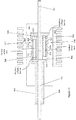
- Figure 1A illustrates a sectional view of a first embodiment of a power semiconductor package.
- the power semiconductor package comprises a substrate 100.
- Figure 1B illustrates a top down plan view of the substrate 100.
- the substrate 100 includes a lowermost metal layer 102, an uppermost metal layer 104, a lower intermediary metal layer 106 and an upper intermediary metal layer 108 above the lower intermediary metal layer 106.
- the lower intermediary metal layer 106 is separated from the lowermost metal layer 102 by a first insulating layer 110.
- the upper intermediary metal layer 108 is separated from the lower intermediary metal layer 106 by a second insulating layer 112, and separated from the uppermost metal layer 104 by a third insulating layer 114.
- the uppermost metal layer 104 is patterned into a plurality of strips 104a-104j which extend in parallel over a width (W) of the substrate 100.
- the power semiconductor package further comprises a first group 116 of semiconductor dies, a second group 118 of semiconductor dies, a third group 120 of semiconductor dies, a fourth group 122 of semiconductor dies, a fifth group 124 of semiconductor dies, and a sixth group 126 of semiconductor dies.
- the first group 116 of semiconductor dies is electrically connected in series to the second group 118 of semiconductor dies to form a first half bridge
- the third group 120 of semiconductor dies is electrically connected in series to the fourth group 122 of semiconductor dies to form a second half bridge
- the fifth group 124 of semiconductor dies is electrically connected in series to the sixth group 126 of semiconductor dies to form a third half bridge to yield a 3-phase inverter.
- FIG. 1A A generic circuit schematic of an exemplary 3-phase inverter is shown in Figure 1A , where device Q1 generically represents the first group 116 of semiconductor dies, device Q2 generically represents the second group 118 of semiconductor dies, etc.
- Each device Q1, Q2, ..., Q6 shown in the circuit schematic is implemented by a plurality of semiconductor dies attached in a row to one strip of the uppermost metal layer 104 of the substrate 100.
- the semiconductor dies can include power MOSFETs (metal-oxide-semiconductor field effect transistors), IGBTs (insulated gate bipolar transistors, SiC or III-V power semiconductor transistors such as GaN transistors, etc.
- the transistor devices can be lateral or vertical devices.
- each group of semiconductor dies is attached to one strip of the uppermost metal layer 104 and evenly distributed over the width of that strip.
- the semiconductor dies in each group are placed side-by-side in a single row and the rows of dies are attached to parallel ones of the metal strips.
- the direction of each row of dies is oriented perpendicular to the current flowing within the parallel plates of the waveguide structure.
- the parallel plate waveguide structure comprises the upper and lower intermediary metal layers 106, 108 of the substrate 100.
- the DC- terminal is electrically connected to the lower intermediary metal layer 106 of the substrate 100 through a plurality of conductive vias 128 that extend through the third and second insulating layers 114, 112.
- the conductive vias 128 are insulated from the upper intermediary metal layer 108.
- the DC+ terminal is electrically connected to the upper intermediary metal layer 108 of the substrate 100 through a plurality of conductive vias 130 that extend through the third insulating layer 114.
- First additional conductive vias 132 extend through the substrate 100 to connect the source (emitter) terminals of the low-side power semiconductor dies represented by devices Q2, Q4 and Q6 in the schematic illustration to the DC- reference plane formed by the lower intermediary metal layer 106.
- Second additional conductive vias 134 extend through the substrate 100 to connect the drain (collector) terminals of the high-side power semiconductor dies represented by devices Q1, Q3 and Q5 in the schematic illustration to the DC+ reference plane formed by the upper intermediary metal layer 108.
- the conductive vias are illustrated as dashed circles in Figure 1B since they are covered by the strips of the uppermost metal layer 104 in this view.
- the position of the intermediary metal layers 106, 108 of the substrate 100 electrically connected to the DC+ and DC- terminals can be switched as would the corresponding conductive vias, to yield an alternative design with the same parallel plate waveguide features. Unbundling the DC power terminals and the layers within the substrate 100 in the way illustrated in Figures 1A and 1B yields a more robust parallel waveguide design with fewer disturbances e.g. due to connections to DC- and DC+ terminals.
- a first AC terminal AC1 is attached to the same strip 104b of the uppermost metal layer 104 as the second group 118 of semiconductor dies and evenly distributed over the width of that strip 104b.
- the source (emitter) of each semiconductor die included in the first group 116 of semiconductor dies is electrically connected to the metal strip 104b to which the first AC terminal AC1 is attached to form the first phase of the 3-phase inverter.
- a second AC terminal AC2 is attached to the same strip 104d of the uppermost metal layer 104 as the fourth group 122 of semiconductor dies and evenly distributed over the width of that strip 104d.
- the source (emitter) of each semiconductor die included in the third group 120 of semiconductor dies is electrically connected to the metal strip 104d to which the second AC terminal AC2 is attached to form the second phase of the 3-phase inverter.
- a third AC terminal AC3 is attached to the same strip 104f of the uppermost metal layer 104 as the sixth group 126 of semiconductor dies and evenly distributed over the width of that strip 104f.
- the source (emitter) of each semiconductor die included in the fifth group 124 of semiconductor dies is electrically connected to the metal strip 104f to which the third AC terminal AC3 is attached to form the third phase of the 3-phase inverter.
- Each DC and AC terminal can be implemented as a separate busbar or as a plurality of pins attached in a row and distributed evenly over the width of the corresponding metal strip of the uppermost metal layer 104.
- the drain (collector) connections of the semiconductor dies are through the bottom side of the respective dies to the corresponding metal strip of the uppermost metal layer 104.
- the gate connections are not shown for ease of illustration.
- a DC-link capacitor (Clink) of the 3-phase inverter can also be integrated into the package design as shown in Figures 1A and 1B .
- the DC link capacitor is implemented as a plurality of capacitor dies coupled in parallel between the DC+ and DC- planes.
- the capacitors are attached to and connect two strips 108a, 108b of the upper intermediary metal layer 108 of the substrate 102. These two strips 108a, 108b of the second intermediary metal layer 108 extend in parallel over a width of the second intermediary metal layer 108.
- the capacitors are evenly distributed over the width of the second intermediary metal layer 108 of the substrate 100 to even current distribution.
- the substrate 100 to which the semiconductor dies of the 3-phase inverter are attached can be any standard substrate having a plurality of metal layers separated by insulating layers.
- the substrate can be a laminate, a ceramic-based substrate such as a DCB (direct copper bonded) substrate, AMB (active metal brazed) substrate, or DAB (direct aluminum bonded) substrate with metallized surfaces, a printed circuit board (PCB), a substrate produced by a chip embedding technology such as eWLB (embedded wafer level ball grid array), etc.
- the semiconductor package embodiment illustrated in Figures 1A and 1B utilizes semiconductor dies having an active backside i.e. vertical devices in which current flows between the front side facing away from the substrate 100 to the backside attached to the substrate 100.
- the semiconductor package embodiments described next utilize semiconductor dies having an insulated or isolated backside, simplifying the design of the parallel plate waveguide.
- Various die configurations are contemplated which have an insulated/isolated backside.
- Figures 2-9 illustrate various exemplary semiconductor die configurations in which the die backside is insulated or isolated from the uppermost metal layer of the package substrate.
- Figure 2 shows a vertical power transistor die such as a power MOSFET or IGBT in which current flows vertically through the active area 200 of the die between the source/emitter (S/E) and the drain/collector (D/C) of the die.
- the amount of current flow is controlled by the voltage applied to the gate terminal (Gate) which is disposed at the front side of the die.
- the source/emitter terminal also is disposed at the front side.
- the drain/collector terminal is disposed at the backside of the active area.
- An insulator 202 such as a dielectric or molding compound covering the bottom side of the drain/collector terminal or a pn junction ensures proper electrical isolation between the drain/collector terminal of the die and the uppermost metal layer of the package substrate.
- the drain/collector terminal is brought up to the front side of the die so that all electrical connections are made at this side of the die.
- a termination / passivation layer 203 is provided at the front side of the die to ensure proper isolation of the die
- Figure 3 shows a lateral power transistor die such as a GaN HEMT (high electron mobility transistor) in which current flows laterally through the active area 204 of the die between the source/emitter and drain/collector of the device. All terminals of the lateral die are formed at the front side of the die i.e. the side of the die facing away from the package substrate.
- An insulator 206 such as a dielectric or molding compound covering the bottom side of the die active area or a pn junction ensures proper electrical isolation between the die and the uppermost metal layer of the package substrate.
- a termination / passivation layer 207 is provided at the front side of the die to ensure proper isolation of the die terminals.
- Figure 4 shows a vertical power diode die in which current flows vertically through the active area 208 of the die between the (top) anode terminal and the (bottom) cathode terminal of the diode.
- an insulator 210 such as a dielectric or molding compound covering the bottom side of the cathode terminal or a pn junction ensures proper electrical isolation between the cathode terminal of the die and the uppermost metal layer of the package substrate.
- the cathode terminal is brought up to the front side of the die so that all electrical connections are made at this side of the die.
- a termination / passivation layer 211 is provided at the front side of the die to ensure proper isolation of the die terminals.
- Figure 5 shows a vertical power diode die similar to the one shown in Figure 4 , however, the position of the anode and cathode terminals are switched so that the cathode terminal is at the front side of the die and the anode terminal is at the backside.
- An insulator 210 such as a dielectric or molding compound covering the bottom side of the anode terminal or a pn junction ensures proper electrical isolation between the anode terminal of the die and the uppermost metal layer of the package substrate.
- the anode terminal is brought up to the front side of the die so that all electrical connections are made at this side of the die.
- Figure 6 shows a vertical transistor die similar to the one shown in Figure 2 , however, the drain/collector terminal is not brought up to the front side of the die. Instead, the drain/collector terminal is contacted at the side of the die and remains isolated from the underlying package substrate by the insulator / pn junction structure 202 formed on the backside of the die.
- Figure 7 shows a vertical diode die similar to the one shown in Figure 4 , however, the cathode terminal is not brought up to the front side of the die. Instead, the cathode terminal is contacted at the side of the die and remains isolated from the underlying package substrate by the insulator / pn junction structure 210 formed on the backside of the die.
- Figure 8 shows a vertical transistor die similar to the one shown in Figure 2 , however, the drain/collector terminal is brought up to the front side of the die along at least two sides of the vertical active area.
- Figure 9 shows a vertical diode die similar to the one shown in Figure 4 , however, the cathode terminal is brought up to the front side of the die along at least two sides of the vertical active area.
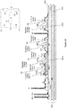
- Figure 10 illustrates a sectional view of another embodiment of a power semiconductor package.
- the power semiconductor package comprises a substrate 300 and two groups 302, 304 of power semiconductor dies each having a backside attached to the substrate 300, the backside of each die being insulated or isolated from the substrate 300 e.g. as previously described herein with respect to Figures 2-9 .
- the substrate 300 includes a lowermost metal layer 306, an uppermost metal layer 308, and at least a first insulating layer 310 separating the lowermost metal layer 306 from the uppermost metal layer 308.
- the uppermost metal layer 308 is patterned into a plurality of strips 308a, 308b which extend in parallel over a width of the substrate 300.
- a first group 302 of the semiconductor dies is attached to a first one of the strips 308a of the uppermost metal layer 308 and evenly distributed over the width of the first strip 308a.
- a second group 304 of the semiconductor dies is attached to the same strip 308a of the uppermost metal layer 308 as the first group 302 of dies, and is evenly distributed over the width of the strip 308a.
- Each semiconductor die in the first and second groups 302, 304 has an insulated or isolated face attached to the first strip 308a e.g. as previously described herein with respect to Figures 2-9 .
- the first group 302 of semiconductor dies is electrically connected in series to the second group 304 of semiconductor dies to form a half bridge circuit.
- FIG. 10 A generic circuit schematic of an exemplary half bridge inverter is shown in Figure 10 , where device Q1 generically represents the first group 302 of semiconductor dies and device Q2 generically represents the second group 304 of semiconductor dies.
- Each device Q1, Q2 shown in the circuit schematic is implemented by a plurality of semiconductor dies attached in a row to one strip 308a of the uppermost metal layer 308 of the substrate 300.
- the semiconductor dies can include power MOSFETs (metal-oxide-semiconductor field effect transistors), IGBTs (insulated gate bipolar transistors, III-V power semiconductor transistors such as GaN transistors, etc.
- the transistor devices can be lateral or vertical devices.
- One or more additional series-connected (half bridge) groups of semiconductor dies can be attached to further strips (not shown) of the uppermost metal layer 308 of the substrate 300 to form a multi-phase inverter e.g. as schematically illustrated in Figures 1A and 1B .
- the circuit can be a multi-level inverter as described later herein.
- a DC+ terminal is attached to the same strip 308a of the uppermost metal layer 308 as the semiconductor dies in the first and second groups 302, 304 and evenly distributed over the width of the metal strip 308a.
- a DC- terminal is attached to a different strip 308b of the uppermost metal layer 308 than the DC+ terminal and evenly distributed over the width of that metal strip 308b. Evenly distributing the semiconductor dies and the DC terminals across the width of the substrate 300 ensures a relatively even spread of current flowing through the parallel plate waveguide structure.
- the bottom plate of the waveguide structure is formed by the uppermost metal layer 308 of the substrate 300.
- the top plate of the waveguide approximates a planar plate design and is formed by bond wire connections 312 to the top metal layer 308 of the substrate 300 and to the power semiconductor dies in the first and second groups 302, 304, and the power semiconductor dies themselves.
- Current enters the uppermost metal layer 308 of the substrate 300 via the DC+ terminal of the package which is attached to the same strip 308b of the uppermost metal layer 308 as the in the first and second groups 302, 304 of semiconductor dies. Current exits through the approximated upper plate via the DC- terminal.
- conductive via connections to intermediary metal layers of the substrate 300 are not needed due to the use of semiconductor dies having an insulated or isolated backside, thus simplifying the substrate design and reducing the number of disturbances in the lower plate of the waveguide structure.
- the drain (collector) terminal of the semiconductor dies in the first group 302 are electrically connected to the same strip 308b of the uppermost metal layer 308 as the DC+ terminal, through a plurality of corresponding bond wire connections 312.
- the source (emitter) terminal of the semiconductor dies in the first group 302 are electrically connected to an additional metal strip 314 separated from the uppermost metal layer 308 of the substrate 300 by an insulating layer 316, through a plurality of corresponding bond wire connections 312.
- the drain (collector) terminal of the semiconductor dies in the second group 304 are electrically connected to the additional metal strip 314 insulated from the uppermost metal layer 308 of the substrate 300, through corresponding bond wire connections 312.
- the source (emitter) terminal of the semiconductor dies in the second group 304 are electrically connected to the same strip 308b of the uppermost metal layer 308 as the DC- terminal, through corresponding bond wire connections 312.
- the AC terminal of the power semiconductor package is attached to the additional metal strip 314 insulated from the uppermost metal layer 308 of the substrate 300.
- Figures 11 through 14 illustrate additional embodiments of power semiconductor packages having a parallel plate waveguide structure and with a pluggable or press-fit type interface.
- Figure 11 illustrates an embodiment of a power semiconductor package that comprises a substrate having a lowermost metal layer 400, an uppermost metal layer 402 and an intermediary metal layer 404 insulated from the uppermost and lowermost metal layers 400, 402 by respective insulating layers 406, 408.
- a first group 410 of semiconductor dies is attached to the bottom side of the intermediary metal layer 404 and evenly distributed over a width of the intermediary metal layer 404.
- Each semiconductor die in the first group 410 has an insulated or isolated face attached to the bottom side of the intermediary metal layer 404 e.g. as previously described herein with respect to Figures 2-9 .
- a second group 412 of semiconductor dies is attached to the top side of the intermediary metal layer 404 and evenly distributed over the width of the intermediary metal layer 404.
- Each semiconductor die in the second group 412 has an insulated or isolated face attached to the second side of the intermediary metal layer 404 e.g. as previously described herein with respect to Figures 2-9 .
- the first group 410 of semiconductor dies is electrically connected in series to the second group 412 of semiconductor dies to form a half bridge circuit.
- a generic circuit schematic of an exemplary half bridge circuit is shown in Figure 11 , where device Q1 generically represents the first group 410 of semiconductor dies and device Q2 generically represents the second group 412 of semiconductor dies.
- Each device Q1, Q2 shown in the circuit schematic is implemented by a plurality of semiconductor dies attached in a row to the intermediary metal layer 404 of the substrate.
- the semiconductor dies can include power MOSFETs (metal-oxide-semiconductor field effect transistors), IGBTs (insulated gate bipolar transistors, III-V power semiconductor transistors such as GaN transistors, etc.
- the transistor devices can be lateral or vertical devices.
- One or more additional series-connected (half bridge) groups of semiconductor dies can be attached to further strips (not shown) of the intermediary metal layer 404 of the substrate to form a multi-phase inverter.
- the circuit can be a multi-level inverter as described later herein.
- the lowermost metal layer 400 of the substrate forms the DC+ terminal of the power semiconductor package and the uppermost metal layer 402 of the substrate forms the DC- terminal of the power semiconductor package.
- the position of the DC+ and DC- terminals can be reversed, to yield an alternative design with the same parallel plate waveguide features.
- the intermediary metal layer 404 of the substrate forms the AC terminal of the power semiconductor package.
- the AC and DC terminals are each evenly distributed over the width of the substrate, to ensure a relatively even spread of current flowing through the parallel plate waveguide structure.
- the intermediary metal layer 404 of the substrate which forms the AC terminal of the half bridge circuit, is partly shielded by the DC+ and DC- terminals and forms part of a 3-layer parallel plate design according to this embodiment.
- the middle plate of the waveguide is formed by the intermediary metal layer 404 of the substrate, the lower plate of the waveguide is formed by the lowermost metal layer 400 of the substrate and the upper plate of the waveguide is formed by the uppermost metal layer 402 of the substrate. If the metal layers 400, 402, 404 of the substrate are spaced close enough and the insulating layers 406, 408 of the substrate are not too thick, low parasitic inductance is realized between the metal layers 400, 402, 404.
- An insulating material 414 such as a plastic molding compound can encapsulate the first and second groups 410, 412 of semiconductor dies, part of the uppermost metal layer 402, part of the lowermost metal layer 400, and part of the intermediary metal layer 404 so that the uppermost metal layer 402, the lowermost metal layer 400 and the intermediary metal layer 404 protrude from the insulating material 414.
- the end of the substrate that protrudes from the insulating material 414 can form a pluggable or press-fit type interface with a correspondingly-shaped connector 416 having metal layers 418 separated by insulating layers 420.
- Cooling can be provided through the intermediary (AC) metal layer 404 of the substrate by integrated channels for liquid or attached heat sinks.
- the intermediary metal layer 404 of the substrate protrudes from opposing sides of the insulating material 414.
- a first heatsink 422 can be attached to the top side of the intermediary metal layer 404 and a second heatsink 424 can be attached to the bottom side of the intermediary metal layer 404.
- Figure 12 illustrates another embodiment of a power semiconductor package having a parallel plate waveguide formed by three metal layers 400, 402, 404 of a substrate.
- the embodiment shown in Figure 12 is similar to the embodiment shown in Figure 11 .
- cooling is provided through the insulating material 414 that encapsulates the semiconductor dies and part of the substrate.
- a first heatsink 500 can be attached to a first (bottom) side of the insulating material 414 covering the first group 410 of semiconductor dies.
- a second heatsink 502 can be attached to a second (top) side of the insulating material 414 covering the second group 412 of semiconductor dies.
- metallization 504 is formed on the insulated/isolated semiconductor dies to provide electrical connections to the DC+, DC- and AC terminals realized by the metal layers 400, 402, 404 of the substrate.
- the metallization 504 can be deposited e.g. by sputtering, electroplating (galvanic deposition), etc.
- a chip embedding technology such as eWLB (embedded wafer level ball grid array) can be used to form the metal and insulating layers 404-408 of the substrate and the metallization 504 that provides electrical connections to the DC+, DC- and AC terminals realized by the metal layers 400, 402, 404 of the substrate.
- Figure 13 illustrates yet another embodiment of a power semiconductor package having a parallel plate waveguide formed by three metal layers 400, 402, 404 of a substrate.
- the embodiment shown in Figure 13 is similar to the embodiment shown in Figure 11 .
- the end of the intermediary metal layer 404 closest to the pluggable / press-fit type interface is covered by an insulating material 506 and therefore not exposed. Electrical contact to the intermediary metal layer 404 of the substrate is made at the opposite end.
- Figure 14 illustrates still another embodiment of a power semiconductor package having a parallel plate waveguide formed by three metal layers 400, 402, 404 of a substrate.
- the embodiment shown in Figure 14 is similar to the embodiment shown in Figure 13 .
- the intermediary metal layer 404 terminates at the end closest to the pluggable / press-fit type interface prior to extending between the uppermost and lowermost metal layers 400, 402 of the substrate. This way, the uppermost and lowermost metal layers 400, 402 are separated from one another by only a single insulating layer 406.
- Figure 15 illustrates an embodiment of a power semiconductor package that comprises a substrate 600 such as a PCB, laminate or substrate formed by a chip embedding technology such as eWLB.
- the substrate 600 has a plurality of metal layers 602, 604, 606, 608 separated from one another by respective insulating layers 610, 612, 614.
- the parallel plate waveguide is formed by the metal layers 602, 604, 606, 608 of the substrate 600.
- Conductive vias 616 within the substrate interconnect the parallel plates.
- a first group 618 of semiconductor dies is attached to a first side of the substrate 600 and evenly distributed over a width of the substrate 600. Each semiconductor die in the first group 618 has all terminals at one side which is attached to the first side of the substrate 600 and an insulated or isolated face at the opposite side e.g. as previously described herein with respect to Figures 2-9 .
- a second group 620 of semiconductor dies is attached to a second side of the substrate 600 opposite the first side and evenly distributed over the width of the substrate 600. Each semiconductor die in the second group 620 has all terminals at one side which is attached to the second side of the substrate 600 and an insulated or isolated face at the opposite side e.g. as previously described herein with respect to Figures 2-9 .
- the first group 618 of semiconductor dies is electrically connected in series to the second group 620 of semiconductor dies to form a half bridge circuit.
- a generic circuit schematic of an exemplary half bridge circuit is shown in Figure 15 , where device Q1 generically represents the first group 618 of semiconductor dies and device Q2 generically represents the second group 620 of semiconductor dies.
- Each device Q1, Q2 shown in the circuit schematic is implemented by a plurality of semiconductor dies attached in a row to one strip of either the uppermost or lowermost metal layer 602/604 of the substrate 600.
- the semiconductor dies can include power MOSFETs (metal-oxide-semiconductor field effect transistors), IGBTs (insulated gate bipolar transistors, III-V power semiconductor transistors such as GaN transistors, etc.
- the transistor devices can be lateral or vertical devices.
- One or more additional series-connected (half bridge) groups of semiconductor dies can be attached to further strips (not shown) of the uppermost and lowermost metal layers 602, 604 of the substrate 604 to form a multi-phase inverter.
- the circuit can be a multi-level inverter as described later herein.
- the lowermost metal layer 602 of the substrate 600 is patterned to form both the DC+ plane of the power semiconductor package and a pathway for carrying gate signals to the semiconductor dies in the first group 618 of dies.
- the uppermost metal layer 604 of the substrate 600 is patterned to form both the DC- plane of the power semiconductor package and a pathway for carrying gate signals to the semiconductor dies in the second group 620 of dies.
- the position of the DC+ and DC- planes within the substrate 600 can be reversed, to yield an alternative design with the same parallel plate waveguide features.
- the AC and DC planes are each evenly distributed over the width of the substrate 600 to ensure a relatively even spread of current flowing through the parallel plate waveguide structure.
- a first heatsink 622 can be attached to the insulated or isolated face of each semiconductor die included in the first group 618 of dies.
- a second heatsink 624 can be attached to the insulated or isolated face of each semiconductor die included in the second group 620 of dies.
- Figure 16 illustrates an embodiment of a power semiconductor package that comprises a substrate 700 having a lowermost metal layer 702, an uppermost metal layer 704, and an intermediary metal layer 706 separated from the lowermost metal layer 702 by a first insulating layer 708 and separated from the uppermost metal layer 704 by a second insulating layer 710.
- the uppermost metal layer 704 is patterned into a plurality of strips 704a-704g which extend in parallel over the width of the substrate 700.
- a first group 712 of semiconductor dies is attached to a first one of the strips 704a of the uppermost metal layer 704 and evenly distributed over the width of the first strip 704a.
- Each semiconductor die in the first group 712 has an insulated or isolated face attached to the first strip 704a e.g. as previously described herein with respect to Figures 2-9 .
- a second group 714 of semiconductor dies is attached to the same first metal strip 704a as the first group 712 of dies and also evenly distributed over the width of the first strip 704a.
- Each semiconductor die in the second group 714 has an insulated or isolated face attached to the first strip 704a e.g. as previously described herein with respect to Figures 2-9 .
- a third group 716 of semiconductor dies is attached to a second one of the strips 704b of the uppermost metal layer 704 and evenly distributed over the width of the second strip 704b.
- Each semiconductor die in the third group 716 has an insulated or isolated face attached to the second strip 704b e.g. as previously described herein with respect to Figures 2-9 .
- a fourth group 718 of semiconductor dies is attached to the same second metal strip 704b as the third group 716 of dies and also evenly distributed over the width of the second strip 704b.
- Each semiconductor die in the fourth group 718 has an insulated or isolated face attached to the second strip 704b e.g. as previously described herein with respect to Figures 2-9 .
- a fifth group 720 of semiconductor dies is attached to a third one of the strips 704c of the uppermost metal layer 704 and evenly distributed over the width of the third strip 704c.
- Each semiconductor die in the fifth group 720 has an insulated or isolated face attached to the third strip 704c e.g. as previously described herein with respect to Figures 2-9 .
- a sixth group 722 of semiconductor dies is attached to the same third metal strip 704c as the fifth group 720 of dies and also evenly distributed over the width of the third strip 704c.
- Each semiconductor die in the sixth group 722 has an insulated or isolated face attached to the third strip 704c e.g. as previously described herein with respect to Figures 2-9 .
- the first group 712 of semiconductor dies is electrically connected in series to the second group 714 of semiconductor dies
- the third group 716 of semiconductor dies is electrically connected in series to the fourth group 718 of semiconductor dies
- the fifth group 720 of semiconductor dies is electrically connected in series to the sixth group 722 of semiconductor dies to form a 3-phase inverter.
- a generic circuit schematic of an exemplary 3-phase inverter is shown in Figure 16 , where device Q1 generically represents the first group 712 of semiconductor dies, device Q2 generically represents the second group 714 of semiconductor dies, etc.
- Each device Q1, Q2, ..., Q6 shown in the circuit schematic is implemented by a plurality of semiconductor dies attached in a row to one strip of the uppermost metal layer 704 of the substrate 700.
- the semiconductor dies can include power MOSFETs (metal-oxide-semiconductor field effect transistors), IGBTs (insulated gate bipolar transistors, III-V power semiconductor transistors such as GaN transistors, etc.
- the transistor devices can be lateral or vertical devices.
- each group of semiconductor dies is evenly distributed in a row over the width of the metal strip to which those dies are attached.
- the direction of each row of dies is oriented perpendicular to the current flowing within the parallel plates of the waveguide structure.
- the parallel plate waveguide structure comprises the uppermost metal layer 704 and the intermediary metal layer 706 of the substrate 700. Current enters the intermediary metal layer 706 via the DC+ terminal of the package which is attached to one of the strips 704g of the uppermost metal layer 704, and current exits through the uppermost metal layer 704 via the DC- terminal.
- the DC+ and DC- terminals are evenly distributed over the width of the corresponding metal strips 704c, 704g to ensure the current is spread relatively evenly across the width of the substrate 700.
- Electrical connections from the drains of the high side transistors represented by devices Q1, Q3 and Q5 in the circuit schematic to the intermediary metal layer 706 of the substrate 700 which forms the DC+ plane are provided by conductive vias 724 which extend through and are insulated from the uppermost metal layer 704 of the substrate 700 and through the upper insulating layer 710 of the substrate 700.
- the position of the DC+ and DC- planes within the substrate 700 can be reversed, to yield an alternative design with the same parallel plate waveguide features. In either case, the DC terminals are each evenly distributed over the width of the substrate 700 to ensure a relatively even spread of current flowing through the parallel plate waveguide structure.
- the AC terminals of the 3-phase inverter are provided above the substrate 700. More particularly, a first AC terminal AC1 is attached to a first additional metal strip 726 disposed over the first strip 704a of the uppermost metal layer 704 of the substrate.
- the first additional metal strip 726 is disposed between the first and second groups 712, 714 of semiconductor dies, extends over the width of the first strip 704a, and is separated from the uppermost metal layer 704 by an insulating layer 728.
- the first AC terminal AC1 is evenly distributed over the width of the first additional metal strip 726.
- a second AC terminal AC2 is attached to a second additional metal strip 730 disposed over the second strip 704b of the uppermost metal layer 704 of the substrate 700.
- the second additional metal strip is disposed between the third and fourth groups 716, 718 of semiconductor dies, extends over the width of the second strip 704b, and is separated from the uppermost metal layer 704 by an insulating layer 732.
- the second AC terminal AC2 is evenly distributed over the width of the second additional metal strip 730.
- a third AC terminal AC3 is attached to a third additional metal strip 734 disposed over the third strip 704c of the uppermost metal layer 704 of the substrate 700.
- the third additional metal strip 734 is disposed between the fifth and sixth groups 720, 722 of semiconductor dies, extends over the width of the third strip 704c, and is separated from the uppermost metal layer 704 by an insulating layer 736.
- the third AC terminal AC3 is evenly distributed over the width of the third additional metal strip 734.
- Each AC terminal can be implemented as a separate busbar or as a plurality of pins attached in a row and distributed evenly over the width of the corresponding additional metal strip disposed above the substrate 700.
- the embodiment illustrated in Figure 16 expands the parallel plate waveguide design illustrated in Figure 10 (half bridge inverter) to accommodate a 3-level topology. Compared to the embodiment illustrated in Figures 1A and 1B , the embodiment illustrated in 16 requires one less insulation layer in the substrate 700 to realize the parallel plate waveguide. The additional insulation layer is omitted due to the use of semiconductor dies having an insulated or isolated face attached to the uppermost metal layer 704 of the substrate 700.
- FIG 17 illustrates an embodiment of a power semiconductor package which is similar to the embodiment shown in Figure 15 .
- the circuit is expanded from a single half bridge inverter to a 3-phase inverter as indicated by the equivalent circuit schematic shown in Figure 17 .
- Each pair of series-connected groups of semiconductor dies is represented by one leg Q1/Q2, Q3/Q4, Q5/Q6 of the 3-phase circuit schematic in Figure 17 .
- Each device Q1, Q2, etc. is implemented by a plurality of semiconductor dies attached in a row to a corresponding strip of the lowermost metal layer 802 of the substrate 800, as previously described herein in connection with Figure 15 .
- all of the semiconductor dies are attached at their respective insulated / isolated side to the same side of the substrate 800.
- the design of the substrate 800 is altered to bring all electrical connections out at the opposite side of the substrate 800 i.e. the side opposite the dies.
- a first intermediary metal layer 804 of the substrate 804 forms the DC+ plane of the power semiconductor package and a second intermediary metal layer 806 of the substrate 800 forms the DC- plane of the power semiconductor package.
- the intermediary metal layers 804, 806 of the substrate 800 are insulated from one another and form the parallel plate waveguide.
- the same heatsink 808 can be attached to the insulated or isolated face of each semiconductor die, which faces away from the substrate 800 in this embodiment.
- FIG 18 illustrates an embodiment of a power semiconductor package which is similar to the embodiments shown in Figures 10 and 16 . Different, however, is the circuit implemented. Instead of a single half bridge or 3-phase inverter, the package implements the 3-level converter schematically illustrated in Figure 18 .
- the 3-level converter has three input and output paths, depending on the controllable commutation paths implemented between the switches and diodes. This way, the AC terminal can be coupled to DC+, DC- or a midpoint level 'N'.
- the midpoint level 'N' is realized between two capacitors C1, C2 connected in series between the DC+ and DC- terminals.
- a first pair of series-connected devices Q1/Q2 provides a controllable path between midpoint level 'N' and the AC terminal.
- a second pair of series-connected devices Q3/Q4 provides a controllable path between either DC+ or DC- and the AC terminal.
- Each device Q1, Q2, Q3, Q4 shown in the circuit schematic is implemented by a plurality of semiconductor dies attached in a row to one strip 902a/902b of the uppermost metal layer 902 of the substrate 900.
- the semiconductor dies can include power MOSFETs (metal-oxide-semiconductor field effect transistors), IGBTs (insulated gate bipolar transistors, III-V power semiconductor transistors such as GaN transistors, etc.
- the transistor devices can be lateral or vertical devices.
- the semiconductor dies that form device Q1 are attached to a first strip 902a of the uppermost metal layer 902 of the substrate 900 and evenly distributed over the width of the first strip 902a.
- the semiconductor dies that form device Q2 are attached to the same first metal strip 902a as the semiconductor dies that form device Q1, and are evenly distributed over the width of the first strip 902a.
- Each semiconductor die that forms device Q1 and each semiconductor die that forms device Q2 has an insulated or isolated face attached to the first metal strip 902a e.g. as previously described herein with respect to Figures 2-9 .
- the semiconductor dies that form device Q1 are electrically connected in series to the semiconductor dies that form device Q2, as illustrated in the corresponding circuit schematic.
- the semiconductor dies that form device Q3 are attached to a second strip 902b of the uppermost metal layer 902 of the substrate 900 and evenly distributed over the width of the second strip 902b.
- the semiconductor dies that form device Q4 are attached to the same second metal strip 902b as the semiconductor dies that form device Q3, and are evenly distributed over the width of the second strip 902b.
- Each semiconductor die that forms device Q1 and each semiconductor die that forms device Q2 has an insulated or isolated face attached to the second metal strip 902b e.g. as previously described herein with respect to Figures 2-9 .
- the semiconductor dies that form device Q1 are electrically connected in series to the semiconductor dies that form device Q2, as illustrated in the corresponding circuit schematic.
- the terminal for the midpoint level 'N' of the 3-level converter circuit is provided above the substrate 900 according to the embodiment illustrated in Figure 18 . More particularly, the terminal for the midpoint level 'N' is attached to an additional metal strip 906 disposed over and insulated from the first strip 902a of the uppermost metal layer 902 of the substrate 900.
- the additional metal strip 906 is disposed between capacitor C2 and the semiconductor dies that form device Q1, extends over the width of the first strip 902a, and is separated from the substrate 900 by an insulating layer 908.
- the parallel plate waveguide is formed by the uppermost metal layer 902 and intermediary metal layer 910 of the substrate 900 according to this embodiment.
- Figure 19 illustrates an embodiment of a power semiconductor package which is similar to the embodiment shown in Figure 18 . Different, however, the terminal for the midpoint level 'N' of the 3-level converter circuit is attached to the top terminal of capacitor C1.
Landscapes
- Semiconductor Integrated Circuits (AREA)
- Physics & Mathematics (AREA)
- Geometry (AREA)
- Engineering & Computer Science (AREA)
- Manufacturing & Machinery (AREA)
- Power Conversion In General (AREA)
Applications Claiming Priority (1)
| Application Number | Priority Date | Filing Date | Title |
|---|---|---|---|
| US15/380,722 US10008411B2 (en) | 2016-12-15 | 2016-12-15 | Parallel plate waveguide for power circuits |
Publications (3)
| Publication Number | Publication Date |
|---|---|
| EP3349249A2 true EP3349249A2 (de) | 2018-07-18 |
| EP3349249A3 EP3349249A3 (de) | 2018-09-26 |
| EP3349249B1 EP3349249B1 (de) | 2021-09-22 |
Family
ID=59235826
Family Applications (1)
| Application Number | Title | Priority Date | Filing Date |
|---|---|---|---|
| EP17206878.5A Active EP3349249B1 (de) | 2016-12-15 | 2017-12-13 | Leistungshalbleitergehäuse mit niedriger parasitärer induktivität |
Country Status (3)
| Country | Link |
|---|---|
| US (3) | US10008411B2 (de) |
| EP (1) | EP3349249B1 (de) |
| CN (1) | CN108231751B (de) |
Cited By (3)
| Publication number | Priority date | Publication date | Assignee | Title |
|---|---|---|---|---|
| EP4080565A1 (de) * | 2021-04-20 | 2022-10-26 | Kabushiki Kaisha Toshiba | Halbleiterbauelement |
| DE102021214906A1 (de) | 2021-10-14 | 2023-04-20 | Vitesco Technologies Germany Gmbh | Elektronische Baugruppe |
| EP4651635A1 (de) * | 2024-05-14 | 2025-11-19 | Rimac Technology LLC | Pcb-schichtstapel und bodenplanung |
Families Citing this family (7)
| Publication number | Priority date | Publication date | Assignee | Title |
|---|---|---|---|---|
| DE102016106359A1 (de) * | 2016-04-07 | 2017-10-12 | Dr. Ing. H.C. F. Porsche Aktiengesellschaft | Modul für einen Multilevelkonverter |
| JP6754387B2 (ja) * | 2018-03-15 | 2020-09-09 | 本田技研工業株式会社 | 電力変換装置 |
| US11350519B2 (en) | 2020-01-22 | 2022-05-31 | Delta Electronics (Shanghai) Co., Ltd. | Power module |
| US11342257B2 (en) | 2020-01-22 | 2022-05-24 | Delta Electronics (Shanghai) Co., Ltd. | Carrier board and power module using same |
| US11967899B2 (en) | 2020-05-22 | 2024-04-23 | Marel Power Solutions | Fluid cooled inverter |
| DE102021203851A1 (de) * | 2021-04-19 | 2022-10-20 | Zf Friedrichshafen Ag | Inverteraufbau eines Elektronikmoduls für einen Elektroantrieb eines Fahrzeugs |
| CN116190360B (zh) * | 2021-11-26 | 2024-09-10 | 比亚迪股份有限公司 | 功率模块和电器设备 |
Citations (1)
| Publication number | Priority date | Publication date | Assignee | Title |
|---|---|---|---|---|
| JP2001223449A (ja) * | 2000-02-09 | 2001-08-17 | Toshiba Corp | 多層プリント基板 |
Family Cites Families (56)
| Publication number | Priority date | Publication date | Assignee | Title |
|---|---|---|---|---|
| FR2483146A1 (fr) | 1980-05-23 | 1981-11-27 | Thomson Csf | Operateur logique rapide, a grande entrance, a fonction logique complexe, utilisant au moins un transistor a effet de champ a faible tension de seuil |
| US4490626A (en) | 1982-07-29 | 1984-12-25 | Irvine Sensors Corporation | Multiplexer circuitry for high density analog signals |
| DE3538933A1 (de) | 1985-11-02 | 1987-05-14 | Bbc Brown Boveri & Cie | Leistungshalbleitermodul |
| DE3937045A1 (de) | 1989-11-07 | 1991-05-08 | Abb Ixys Semiconductor Gmbh | Leistungshalbleitermodul |
| US5038267A (en) | 1990-05-03 | 1991-08-06 | General Electric Company | Soft-switching power converter for operation in discrete pulse modulation and pulse width modulation modes |
| EP0469172B1 (de) | 1990-08-02 | 1995-01-25 | Asea Brown Boveri Ag | Viertelbrückenschaltung für grosse Ströme |
| US5261747A (en) | 1992-06-22 | 1993-11-16 | Trustees Of Dartmouth College | Switchable thermoelectric element and array |
| JPH06275677A (ja) | 1993-03-23 | 1994-09-30 | Shinko Electric Ind Co Ltd | 半導体装置用パッケージおよび半導体装置 |
| DE4421319A1 (de) | 1994-06-17 | 1995-12-21 | Abb Management Ag | Niederinduktives Leistungshalbleitermodul |
| US6794836B2 (en) | 2001-02-06 | 2004-09-21 | Invacare Corporation | Electric motor drive controller with voltage control circuit operative in different modes |
| KR101137576B1 (ko) | 2002-07-31 | 2012-04-19 | 에스엠씨 일렉트리칼 프로덕츠, 인크 | 중간 내지 고 전압의 3레벨 이상의 ac 구동 인버터 브리지를 구동하는 저 전압 2레벨 6펄스 인덕션 모터 제어기 |
| JP4479990B2 (ja) * | 2003-10-10 | 2010-06-09 | 学校法人慶應義塾 | 電力変換器及び電力変換器を用いたシステム |
| US7561446B1 (en) | 2005-09-15 | 2009-07-14 | Vlt, Inc. | Double-clamped ZVS buck-boost power converter |
| DE102005007373B4 (de) | 2005-02-17 | 2013-05-29 | Infineon Technologies Ag | Leistungshalbleiterbaugruppe |
| DE102005036116B4 (de) | 2005-08-01 | 2012-03-22 | Infineon Technologies Ag | Leistungshalbleitermodul |
| CA2533000C (en) | 2005-12-08 | 2011-07-05 | Alwin Manufacturing Co., Inc | Method and apparatus for controlling a dispenser and detecting a user |
| DE102006001874B4 (de) | 2006-01-13 | 2012-05-24 | Infineon Technologies Ag | Verfahren und Vorrichtung zur Strom- und Temperaturmessung in einer leistungselektronischen Schaltung |
| US8680666B2 (en) | 2006-05-24 | 2014-03-25 | International Rectifier Corporation | Bond wireless power module with double-sided single device cooling and immersion bath cooling |
| DE102006038479B4 (de) | 2006-08-17 | 2011-01-27 | Infineon Technologies Ag | Leistungshalbleitermodul mit zwei Mehrfach-Leistungshalbleiterbauelementen |
| US7466185B2 (en) | 2006-10-23 | 2008-12-16 | Infineon Technologies Ag | IGBT-Driver circuit for desaturated turn-off with high desaturation level |
| US8026572B2 (en) | 2006-12-06 | 2011-09-27 | Denso Corporation | Semiconductor device and method for manufacturing same |
| JP4436843B2 (ja) | 2007-02-07 | 2010-03-24 | 株式会社日立製作所 | 電力変換装置 |
| US8154114B2 (en) | 2007-08-06 | 2012-04-10 | Infineon Technologies Ag | Power semiconductor module |
| US8018047B2 (en) | 2007-08-06 | 2011-09-13 | Infineon Technologies Ag | Power semiconductor module including a multilayer substrate |
| US7791208B2 (en) | 2007-09-27 | 2010-09-07 | Infineon Technologies Ag | Power semiconductor arrangement |
| WO2009068698A1 (es) | 2007-11-30 | 2009-06-04 | Ingeteam Energy, S.A. | Circuito electrico para convertir energia electrica continua en energia electrica alterna |
| CN101889385B (zh) | 2007-12-07 | 2013-05-29 | 奥斯兰姆有限公司 | 具有倍流整流器的谐振功率转换器及相关方法 |
| JP5444619B2 (ja) * | 2008-02-07 | 2014-03-19 | 株式会社ジェイテクト | 多層回路基板およびモータ駆動回路基板 |
| US7808100B2 (en) | 2008-04-21 | 2010-10-05 | Infineon Technologies Ag | Power semiconductor module with pressure element and method for fabricating a power semiconductor module with a pressure element |
| US7766337B2 (en) | 2008-08-19 | 2010-08-03 | Soarex, Inc. | Game apparatus |
| ES2334628B1 (es) | 2008-09-11 | 2011-01-07 | Ingeteam Technology, S.A | Dispositivo y procedimiento de control para recuperacion de energia cinetica en sistemas ferroviarios. |
| DE102008047028B4 (de) | 2008-09-13 | 2011-06-09 | Infineon Technologies Ag | Schaltungsanordnung zur Ansteuerung eines Leistungshalbleiterschalters und Halbleitermodul |
| DE102008049677B4 (de) | 2008-09-30 | 2014-09-18 | Infineon Technologies Ag | Spannungsversorgung in einer Schaltungsanordnung mit einem Halbleiterschaltelement |
| DE102008055157A1 (de) | 2008-12-23 | 2010-06-24 | Infineon Technologies Ag | Ansteuerschaltung für eine Leistungshalbleiteranordnung und Leistungshalbleiteranordnung |
| IT1393717B1 (it) | 2009-03-31 | 2012-05-08 | Meta System Spa | Dispositivo e metodo per la conversione di corrente continua in corrente alternata |
| JP4977165B2 (ja) * | 2009-04-01 | 2012-07-18 | トヨタ自動車株式会社 | 3相ブラシレスモータのノイズ低減構造 |
| ATE528856T1 (de) * | 2009-06-19 | 2011-10-15 | Vincotech Holdings S A R L | Leistungsmodul mit zusätzlichem transientem strompfad und leistungsmodulsystem |
| JP5461899B2 (ja) | 2009-06-26 | 2014-04-02 | 株式会社東芝 | 電力変換装置 |
| DE102009045181B4 (de) | 2009-09-30 | 2020-07-09 | Infineon Technologies Ag | Leistungshalbleitermodul |
| IT1396963B1 (it) | 2009-10-20 | 2012-12-20 | Meta System Spa | Sistema e metodo per la compensazione dello sbilanciamento delle tensioni in ingresso in inverter multilivello o simili |
| DE102009046258B3 (de) | 2009-10-30 | 2011-07-07 | Infineon Technologies AG, 85579 | Leistungshalbleitermodul und Verfahren zum Betrieb eines Leistungshalbleitermoduls |
| DE102010002627B4 (de) | 2010-03-05 | 2023-10-05 | Infineon Technologies Ag | Niederinduktive Leistungshalbleiterbaugruppen |
| US8581343B1 (en) * | 2010-07-06 | 2013-11-12 | International Rectifier Corporation | Electrical connectivity for circuit applications |
| US8779730B2 (en) | 2010-07-30 | 2014-07-15 | Abb Technology Ag | Capacitor discharge in a cell based voltage source converter |
| US8729914B2 (en) | 2010-11-10 | 2014-05-20 | Infineon Technologies Ag | Detection of the conduction state of an RC-IGBT |
| US8441128B2 (en) | 2011-08-16 | 2013-05-14 | Infineon Technologies Ag | Semiconductor arrangement |
| US8963321B2 (en) | 2011-09-12 | 2015-02-24 | Infineon Technologies Ag | Semiconductor device including cladded base plate |
| US8519532B2 (en) | 2011-09-12 | 2013-08-27 | Infineon Technologies Ag | Semiconductor device including cladded base plate |
| US8487407B2 (en) | 2011-10-13 | 2013-07-16 | Infineon Technologies Ag | Low impedance gate control method and apparatus |
| JP6155282B2 (ja) * | 2012-12-13 | 2017-06-28 | 株式会社日立製作所 | パワー半導体モジュール及びこれを用いた電力変換装置 |
| US9324642B2 (en) * | 2013-11-12 | 2016-04-26 | Infineon Technologies Ag | Method of electrically isolating shared leads of a lead frame strip |
| US9401682B2 (en) * | 2014-04-17 | 2016-07-26 | Freescale Semiconductor, Inc. | Structure for a radio frequency power amplifier module within a radio frequency power amplifier package |
| DE102014110617B4 (de) * | 2014-07-28 | 2023-05-04 | Infineon Technologies Ag | Leistungshalbleitermodulsystem mit hoher Isolationsfestigkeit und Verfahren zur Herstellung einer Leistungshalbleitermodulanordnung mit einer hohen Isolationsfestigkeit |
| WO2016103324A1 (ja) | 2014-12-22 | 2016-06-30 | 三菱電機株式会社 | 電力変換装置および電力用半導体モジュール |
| DE102015101086B4 (de) | 2015-01-26 | 2018-04-12 | Infineon Technologies Ag | Leistungshalbleitermodulanordnung |
| DE102015115271B4 (de) | 2015-09-10 | 2021-07-15 | Infineon Technologies Ag | Elektronikbaugruppe mit entstörkondensatoren und verfahren zum betrieb der elektronikbaugruppe |
-
2016
- 2016-12-15 US US15/380,722 patent/US10008411B2/en active Active
-
2017
- 2017-12-13 EP EP17206878.5A patent/EP3349249B1/de active Active
- 2017-12-15 CN CN201711350774.7A patent/CN108231751B/zh active Active
-
2018
- 2018-05-30 US US15/993,029 patent/US10453742B2/en active Active
- 2018-05-30 US US15/993,173 patent/US10319631B2/en active Active
Patent Citations (1)
| Publication number | Priority date | Publication date | Assignee | Title |
|---|---|---|---|---|
| JP2001223449A (ja) * | 2000-02-09 | 2001-08-17 | Toshiba Corp | 多層プリント基板 |
Cited By (4)
| Publication number | Priority date | Publication date | Assignee | Title |
|---|---|---|---|---|
| EP4080565A1 (de) * | 2021-04-20 | 2022-10-26 | Kabushiki Kaisha Toshiba | Halbleiterbauelement |
| US11764141B2 (en) | 2021-04-20 | 2023-09-19 | Kabushiki Kaisha Toshiba | Semiconductor device |
| DE102021214906A1 (de) | 2021-10-14 | 2023-04-20 | Vitesco Technologies Germany Gmbh | Elektronische Baugruppe |
| EP4651635A1 (de) * | 2024-05-14 | 2025-11-19 | Rimac Technology LLC | Pcb-schichtstapel und bodenplanung |
Also Published As
| Publication number | Publication date |
|---|---|
| US10453742B2 (en) | 2019-10-22 |
| US10319631B2 (en) | 2019-06-11 |
| CN108231751A (zh) | 2018-06-29 |
| CN108231751B (zh) | 2021-06-22 |
| US20170194200A1 (en) | 2017-07-06 |
| US20180277425A1 (en) | 2018-09-27 |
| US10008411B2 (en) | 2018-06-26 |
| US20180286745A1 (en) | 2018-10-04 |
| EP3349249A3 (de) | 2018-09-26 |
| EP3349249B1 (de) | 2021-09-22 |
Similar Documents
| Publication | Publication Date | Title |
|---|---|---|
| EP3349249B1 (de) | Leistungshalbleitergehäuse mit niedriger parasitärer induktivität | |
| US10410952B2 (en) | Power semiconductor packages having a substrate with two or more metal layers and one or more polymer-based insulating layers for separating the metal layers | |
| US10070528B2 (en) | Semiconductor device wiring pattern and connections | |
| US10483216B2 (en) | Power module and fabrication method for the same | |
| US8742490B2 (en) | Vertical power transistor die packages and associated methods of manufacturing | |
| US9972569B2 (en) | Robust low inductance power module package | |
| EP3355351B1 (de) | Interdigit-vorrichtung auf leiterrahmen für gleichmässig verteilten stromfluss | |
| US9196510B2 (en) | Semiconductor package comprising two semiconductor modules and laterally extending connectors | |
| EP3005417A1 (de) | Integration von leistungswandlern mit mehreren ausgängen und vertikal gestapelten halbleiterchips | |
| US20070229143A1 (en) | Power Module | |
| US20240322697A1 (en) | Power semiconductor module and power electronics device | |
| KR20220044502A (ko) | 반도체 장치 | |
| US11973065B2 (en) | Semiconductor arrangements | |
| US20170213806A1 (en) | Semiconductor device | |
| KR101754923B1 (ko) | 고 전자이동도 트랜지스터 기반 전력 모듈 | |
| US12557671B2 (en) | Power semiconductor module and method of producing a power semiconductor module | |
| EP4369394A1 (de) | Leistungshalbleitergehäuse und verfahren zu seiner herstellung | |
| US20250167100A1 (en) | Packaged electronic device having high thermal dissipation comprising a plurality of power transistors and manufacturing process therof | |
| EP4639625A1 (de) | Leistungshalbleitermodul | |
| CN119054072A (zh) | 用于微电子器件的夹层封装件 |
Legal Events
| Date | Code | Title | Description |
|---|---|---|---|
| PUAI | Public reference made under article 153(3) epc to a published international application that has entered the european phase |
Free format text: ORIGINAL CODE: 0009012 |
|
| STAA | Information on the status of an ep patent application or granted ep patent |
Free format text: STATUS: THE APPLICATION HAS BEEN PUBLISHED |
|
| AK | Designated contracting states |
Kind code of ref document: A2 Designated state(s): AL AT BE BG CH CY CZ DE DK EE ES FI FR GB GR HR HU IE IS IT LI LT LU LV MC MK MT NL NO PL PT RO RS SE SI SK SM TR |
|
| AX | Request for extension of the european patent |
Extension state: BA ME |
|
| PUAL | Search report despatched |
Free format text: ORIGINAL CODE: 0009013 |
|
| AK | Designated contracting states |
Kind code of ref document: A3 Designated state(s): AL AT BE BG CH CY CZ DE DK EE ES FI FR GB GR HR HU IE IS IT LI LT LU LV MC MK MT NL NO PL PT RO RS SE SI SK SM TR |
|
| AX | Request for extension of the european patent |
Extension state: BA ME |
|
| RIC1 | Information provided on ipc code assigned before grant |
Ipc: H02M 7/00 20060101ALI20180820BHEP Ipc: H05K 1/02 20060101ALI20180820BHEP Ipc: H01L 23/367 20060101ALI20180820BHEP Ipc: H01L 23/538 20060101ALI20180820BHEP Ipc: H01L 25/07 20060101AFI20180820BHEP Ipc: H01L 23/64 20060101ALI20180820BHEP |
|
| STAA | Information on the status of an ep patent application or granted ep patent |
Free format text: STATUS: REQUEST FOR EXAMINATION WAS MADE |
|
| 17P | Request for examination filed |
Effective date: 20190322 |
|
| RBV | Designated contracting states (corrected) |
Designated state(s): AL AT BE BG CH CY CZ DE DK EE ES FI FR GB GR HR HU IE IS IT LI LT LU LV MC MK MT NL NO PL PT RO RS SE SI SK SM TR |
|
| STAA | Information on the status of an ep patent application or granted ep patent |
Free format text: STATUS: EXAMINATION IS IN PROGRESS |
|
| 17Q | First examination report despatched |
Effective date: 20200903 |
|
| GRAP | Despatch of communication of intention to grant a patent |
Free format text: ORIGINAL CODE: EPIDOSNIGR1 |
|
| STAA | Information on the status of an ep patent application or granted ep patent |
Free format text: STATUS: GRANT OF PATENT IS INTENDED |
|
| RIC1 | Information provided on ipc code assigned before grant |
Ipc: H02M 7/00 20060101ALN20210519BHEP Ipc: H05K 3/46 20060101ALN20210519BHEP Ipc: H01L 23/367 20060101ALI20210519BHEP Ipc: H01L 23/538 20060101ALI20210519BHEP Ipc: H01L 23/64 20060101ALI20210519BHEP Ipc: H05K 1/02 20060101ALI20210519BHEP Ipc: H01L 25/07 20060101AFI20210519BHEP |
|
| RIC1 | Information provided on ipc code assigned before grant |
Ipc: H02M 7/00 20060101ALN20210525BHEP Ipc: H05K 3/46 20060101ALN20210525BHEP Ipc: H01L 23/367 20060101ALI20210525BHEP Ipc: H01L 23/538 20060101ALI20210525BHEP Ipc: H01L 23/64 20060101ALI20210525BHEP Ipc: H05K 1/02 20060101ALI20210525BHEP Ipc: H01L 25/07 20060101AFI20210525BHEP |
|
| INTG | Intention to grant announced |
Effective date: 20210608 |
|
| GRAS | Grant fee paid |
Free format text: ORIGINAL CODE: EPIDOSNIGR3 |
|
| GRAA | (expected) grant |
Free format text: ORIGINAL CODE: 0009210 |
|
| STAA | Information on the status of an ep patent application or granted ep patent |
Free format text: STATUS: THE PATENT HAS BEEN GRANTED |
|
| AK | Designated contracting states |
Kind code of ref document: B1 Designated state(s): AL AT BE BG CH CY CZ DE DK EE ES FI FR GB GR HR HU IE IS IT LI LT LU LV MC MK MT NL NO PL PT RO RS SE SI SK SM TR |
|
| REG | Reference to a national code |
Ref country code: GB Ref legal event code: FG4D |
|
| REG | Reference to a national code |
Ref country code: IE Ref legal event code: FG4D |
|
| REG | Reference to a national code |
Ref country code: DE Ref legal event code: R096 Ref document number: 602017046313 Country of ref document: DE |
|
| REG | Reference to a national code |
Ref country code: CH Ref legal event code: EP Ref country code: AT Ref legal event code: REF Ref document number: 1432975 Country of ref document: AT Kind code of ref document: T Effective date: 20211015 |
|
| REG | Reference to a national code |
Ref country code: LT Ref legal event code: MG9D |
|
| REG | Reference to a national code |
Ref country code: NL Ref legal event code: MP Effective date: 20210922 |
|
| PG25 | Lapsed in a contracting state [announced via postgrant information from national office to epo] |
Ref country code: SE Free format text: LAPSE BECAUSE OF FAILURE TO SUBMIT A TRANSLATION OF THE DESCRIPTION OR TO PAY THE FEE WITHIN THE PRESCRIBED TIME-LIMIT Effective date: 20210922 Ref country code: RS Free format text: LAPSE BECAUSE OF FAILURE TO SUBMIT A TRANSLATION OF THE DESCRIPTION OR TO PAY THE FEE WITHIN THE PRESCRIBED TIME-LIMIT Effective date: 20210922 Ref country code: HR Free format text: LAPSE BECAUSE OF FAILURE TO SUBMIT A TRANSLATION OF THE DESCRIPTION OR TO PAY THE FEE WITHIN THE PRESCRIBED TIME-LIMIT Effective date: 20210922 Ref country code: LT Free format text: LAPSE BECAUSE OF FAILURE TO SUBMIT A TRANSLATION OF THE DESCRIPTION OR TO PAY THE FEE WITHIN THE PRESCRIBED TIME-LIMIT Effective date: 20210922 Ref country code: BG Free format text: LAPSE BECAUSE OF FAILURE TO SUBMIT A TRANSLATION OF THE DESCRIPTION OR TO PAY THE FEE WITHIN THE PRESCRIBED TIME-LIMIT Effective date: 20211222 Ref country code: NO Free format text: LAPSE BECAUSE OF FAILURE TO SUBMIT A TRANSLATION OF THE DESCRIPTION OR TO PAY THE FEE WITHIN THE PRESCRIBED TIME-LIMIT Effective date: 20211222 Ref country code: FI Free format text: LAPSE BECAUSE OF FAILURE TO SUBMIT A TRANSLATION OF THE DESCRIPTION OR TO PAY THE FEE WITHIN THE PRESCRIBED TIME-LIMIT Effective date: 20210922 |
|
| REG | Reference to a national code |
Ref country code: AT Ref legal event code: MK05 Ref document number: 1432975 Country of ref document: AT Kind code of ref document: T Effective date: 20210922 |
|
| PG25 | Lapsed in a contracting state [announced via postgrant information from national office to epo] |
Ref country code: LV Free format text: LAPSE BECAUSE OF FAILURE TO SUBMIT A TRANSLATION OF THE DESCRIPTION OR TO PAY THE FEE WITHIN THE PRESCRIBED TIME-LIMIT Effective date: 20210922 Ref country code: GR Free format text: LAPSE BECAUSE OF FAILURE TO SUBMIT A TRANSLATION OF THE DESCRIPTION OR TO PAY THE FEE WITHIN THE PRESCRIBED TIME-LIMIT Effective date: 20211223 |
|
| PG25 | Lapsed in a contracting state [announced via postgrant information from national office to epo] |
Ref country code: AT Free format text: LAPSE BECAUSE OF FAILURE TO SUBMIT A TRANSLATION OF THE DESCRIPTION OR TO PAY THE FEE WITHIN THE PRESCRIBED TIME-LIMIT Effective date: 20210922 |
|
| PG25 | Lapsed in a contracting state [announced via postgrant information from national office to epo] |
Ref country code: IS Free format text: LAPSE BECAUSE OF FAILURE TO SUBMIT A TRANSLATION OF THE DESCRIPTION OR TO PAY THE FEE WITHIN THE PRESCRIBED TIME-LIMIT Effective date: 20220122 Ref country code: SK Free format text: LAPSE BECAUSE OF FAILURE TO SUBMIT A TRANSLATION OF THE DESCRIPTION OR TO PAY THE FEE WITHIN THE PRESCRIBED TIME-LIMIT Effective date: 20210922 Ref country code: RO Free format text: LAPSE BECAUSE OF FAILURE TO SUBMIT A TRANSLATION OF THE DESCRIPTION OR TO PAY THE FEE WITHIN THE PRESCRIBED TIME-LIMIT Effective date: 20210922 Ref country code: PT Free format text: LAPSE BECAUSE OF FAILURE TO SUBMIT A TRANSLATION OF THE DESCRIPTION OR TO PAY THE FEE WITHIN THE PRESCRIBED TIME-LIMIT Effective date: 20220124 Ref country code: PL Free format text: LAPSE BECAUSE OF FAILURE TO SUBMIT A TRANSLATION OF THE DESCRIPTION OR TO PAY THE FEE WITHIN THE PRESCRIBED TIME-LIMIT Effective date: 20210922 Ref country code: NL Free format text: LAPSE BECAUSE OF FAILURE TO SUBMIT A TRANSLATION OF THE DESCRIPTION OR TO PAY THE FEE WITHIN THE PRESCRIBED TIME-LIMIT Effective date: 20210922 Ref country code: ES Free format text: LAPSE BECAUSE OF FAILURE TO SUBMIT A TRANSLATION OF THE DESCRIPTION OR TO PAY THE FEE WITHIN THE PRESCRIBED TIME-LIMIT Effective date: 20210922 Ref country code: EE Free format text: LAPSE BECAUSE OF FAILURE TO SUBMIT A TRANSLATION OF THE DESCRIPTION OR TO PAY THE FEE WITHIN THE PRESCRIBED TIME-LIMIT Effective date: 20210922 Ref country code: CZ Free format text: LAPSE BECAUSE OF FAILURE TO SUBMIT A TRANSLATION OF THE DESCRIPTION OR TO PAY THE FEE WITHIN THE PRESCRIBED TIME-LIMIT Effective date: 20210922 Ref country code: AL Free format text: LAPSE BECAUSE OF FAILURE TO SUBMIT A TRANSLATION OF THE DESCRIPTION OR TO PAY THE FEE WITHIN THE PRESCRIBED TIME-LIMIT Effective date: 20210922 |
|
| REG | Reference to a national code |
Ref country code: DE Ref legal event code: R097 Ref document number: 602017046313 Country of ref document: DE |
|
| PG25 | Lapsed in a contracting state [announced via postgrant information from national office to epo] |
Ref country code: MC Free format text: LAPSE BECAUSE OF FAILURE TO SUBMIT A TRANSLATION OF THE DESCRIPTION OR TO PAY THE FEE WITHIN THE PRESCRIBED TIME-LIMIT Effective date: 20210922 Ref country code: DK Free format text: LAPSE BECAUSE OF FAILURE TO SUBMIT A TRANSLATION OF THE DESCRIPTION OR TO PAY THE FEE WITHIN THE PRESCRIBED TIME-LIMIT Effective date: 20210922 |
|
| PLBE | No opposition filed within time limit |
Free format text: ORIGINAL CODE: 0009261 |
|
| REG | Reference to a national code |
Ref country code: CH Ref legal event code: PL |
|
| STAA | Information on the status of an ep patent application or granted ep patent |
Free format text: STATUS: NO OPPOSITION FILED WITHIN TIME LIMIT |
|
| GBPC | Gb: european patent ceased through non-payment of renewal fee |
Effective date: 20211222 |
|
| 26N | No opposition filed |
Effective date: 20220623 |
|
| REG | Reference to a national code |
Ref country code: BE Ref legal event code: MM Effective date: 20211231 |
|
| PG25 | Lapsed in a contracting state [announced via postgrant information from national office to epo] |
Ref country code: LU Free format text: LAPSE BECAUSE OF NON-PAYMENT OF DUE FEES Effective date: 20211213 Ref country code: IE Free format text: LAPSE BECAUSE OF NON-PAYMENT OF DUE FEES Effective date: 20211213 Ref country code: GB Free format text: LAPSE BECAUSE OF NON-PAYMENT OF DUE FEES Effective date: 20211222 |
|
| PG25 | Lapsed in a contracting state [announced via postgrant information from national office to epo] |
Ref country code: SI Free format text: LAPSE BECAUSE OF FAILURE TO SUBMIT A TRANSLATION OF THE DESCRIPTION OR TO PAY THE FEE WITHIN THE PRESCRIBED TIME-LIMIT Effective date: 20210922 Ref country code: FR Free format text: LAPSE BECAUSE OF NON-PAYMENT OF DUE FEES Effective date: 20211231 Ref country code: BE Free format text: LAPSE BECAUSE OF NON-PAYMENT OF DUE FEES Effective date: 20211231 |
|
| PG25 | Lapsed in a contracting state [announced via postgrant information from national office to epo] |
Ref country code: LI Free format text: LAPSE BECAUSE OF NON-PAYMENT OF DUE FEES Effective date: 20211231 Ref country code: CH Free format text: LAPSE BECAUSE OF NON-PAYMENT OF DUE FEES Effective date: 20211231 |
|
| PG25 | Lapsed in a contracting state [announced via postgrant information from national office to epo] |
Ref country code: IT Free format text: LAPSE BECAUSE OF FAILURE TO SUBMIT A TRANSLATION OF THE DESCRIPTION OR TO PAY THE FEE WITHIN THE PRESCRIBED TIME-LIMIT Effective date: 20210922 |
|
| PG25 | Lapsed in a contracting state [announced via postgrant information from national office to epo] |
Ref country code: HU Free format text: LAPSE BECAUSE OF FAILURE TO SUBMIT A TRANSLATION OF THE DESCRIPTION OR TO PAY THE FEE WITHIN THE PRESCRIBED TIME-LIMIT; INVALID AB INITIO Effective date: 20171213 |
|
| PG25 | Lapsed in a contracting state [announced via postgrant information from national office to epo] |
Ref country code: CY Free format text: LAPSE BECAUSE OF FAILURE TO SUBMIT A TRANSLATION OF THE DESCRIPTION OR TO PAY THE FEE WITHIN THE PRESCRIBED TIME-LIMIT Effective date: 20210922 |
|
| P01 | Opt-out of the competence of the unified patent court (upc) registered |
Effective date: 20230528 |
|
| PG25 | Lapsed in a contracting state [announced via postgrant information from national office to epo] |
Ref country code: SM Free format text: LAPSE BECAUSE OF FAILURE TO SUBMIT A TRANSLATION OF THE DESCRIPTION OR TO PAY THE FEE WITHIN THE PRESCRIBED TIME-LIMIT Effective date: 20210922 |
|
| PG25 | Lapsed in a contracting state [announced via postgrant information from national office to epo] |
Ref country code: MK Free format text: LAPSE BECAUSE OF FAILURE TO SUBMIT A TRANSLATION OF THE DESCRIPTION OR TO PAY THE FEE WITHIN THE PRESCRIBED TIME-LIMIT Effective date: 20210922 |
|
| PG25 | Lapsed in a contracting state [announced via postgrant information from national office to epo] |
Ref country code: TR Free format text: LAPSE BECAUSE OF FAILURE TO SUBMIT A TRANSLATION OF THE DESCRIPTION OR TO PAY THE FEE WITHIN THE PRESCRIBED TIME-LIMIT Effective date: 20210922 |
|
| PG25 | Lapsed in a contracting state [announced via postgrant information from national office to epo] |
Ref country code: MT Free format text: LAPSE BECAUSE OF FAILURE TO SUBMIT A TRANSLATION OF THE DESCRIPTION OR TO PAY THE FEE WITHIN THE PRESCRIBED TIME-LIMIT Effective date: 20210922 |
|
| REG | Reference to a national code |
Ref country code: DE Ref legal event code: R079 Ref document number: 602017046313 Country of ref document: DE Free format text: PREVIOUS MAIN CLASS: H01L0025070000 Ipc: H10D0080200000 |
|
| PGFP | Annual fee paid to national office [announced via postgrant information from national office to epo] |
Ref country code: DE Payment date: 20260224 Year of fee payment: 9 |