EP3343545B1 - Anzeigetafel mit gate-treiber und verfahren zur steuerung eines gate-treibers - Google Patents
Anzeigetafel mit gate-treiber und verfahren zur steuerung eines gate-treibers Download PDFInfo
- Publication number
- EP3343545B1 EP3343545B1 EP17182793.4A EP17182793A EP3343545B1 EP 3343545 B1 EP3343545 B1 EP 3343545B1 EP 17182793 A EP17182793 A EP 17182793A EP 3343545 B1 EP3343545 B1 EP 3343545B1
- Authority
- EP
- European Patent Office
- Prior art keywords
- area
- clock signal
- stages
- pixels
- stage
- Prior art date
- Legal status (The legal status is an assumption and is not a legal conclusion. Google has not performed a legal analysis and makes no representation as to the accuracy of the status listed.)
- Active
Links
Images





Classifications
-
- G—PHYSICS
- G09—EDUCATION; CRYPTOGRAPHY; DISPLAY; ADVERTISING; SEALS
- G09G—ARRANGEMENTS OR CIRCUITS FOR CONTROL OF INDICATING DEVICES USING STATIC MEANS TO PRESENT VARIABLE INFORMATION
- G09G3/00—Control arrangements or circuits, of interest only in connection with visual indicators other than cathode-ray tubes
- G09G3/20—Control arrangements or circuits, of interest only in connection with visual indicators other than cathode-ray tubes for presentation of an assembly of a number of characters, e.g. a page, by composing the assembly by combination of individual elements arranged in a matrix no fixed position being assigned to or needed to be assigned to the individual characters or partial characters
- G09G3/22—Control arrangements or circuits, of interest only in connection with visual indicators other than cathode-ray tubes for presentation of an assembly of a number of characters, e.g. a page, by composing the assembly by combination of individual elements arranged in a matrix no fixed position being assigned to or needed to be assigned to the individual characters or partial characters using controlled light sources
- G09G3/30—Control arrangements or circuits, of interest only in connection with visual indicators other than cathode-ray tubes for presentation of an assembly of a number of characters, e.g. a page, by composing the assembly by combination of individual elements arranged in a matrix no fixed position being assigned to or needed to be assigned to the individual characters or partial characters using controlled light sources using electroluminescent panels
- G09G3/32—Control arrangements or circuits, of interest only in connection with visual indicators other than cathode-ray tubes for presentation of an assembly of a number of characters, e.g. a page, by composing the assembly by combination of individual elements arranged in a matrix no fixed position being assigned to or needed to be assigned to the individual characters or partial characters using controlled light sources using electroluminescent panels semiconductive, e.g. using light-emitting diodes [LED]
- G09G3/3208—Control arrangements or circuits, of interest only in connection with visual indicators other than cathode-ray tubes for presentation of an assembly of a number of characters, e.g. a page, by composing the assembly by combination of individual elements arranged in a matrix no fixed position being assigned to or needed to be assigned to the individual characters or partial characters using controlled light sources using electroluminescent panels semiconductive, e.g. using light-emitting diodes [LED] organic, e.g. using organic light-emitting diodes [OLED]
- G09G3/3266—Details of drivers for scan electrodes
-
- G—PHYSICS
- G06—COMPUTING OR CALCULATING; COUNTING
- G06F—ELECTRIC DIGITAL DATA PROCESSING
- G06F3/00—Input arrangements for transferring data to be processed into a form capable of being handled by the computer; Output arrangements for transferring data from processing unit to output unit, e.g. interface arrangements
- G06F3/14—Digital output to display device ; Cooperation and interconnection of the display device with other functional units
- G06F3/147—Digital output to display device ; Cooperation and interconnection of the display device with other functional units using display panels
-
- G—PHYSICS
- G09—EDUCATION; CRYPTOGRAPHY; DISPLAY; ADVERTISING; SEALS
- G09G—ARRANGEMENTS OR CIRCUITS FOR CONTROL OF INDICATING DEVICES USING STATIC MEANS TO PRESENT VARIABLE INFORMATION
- G09G3/00—Control arrangements or circuits, of interest only in connection with visual indicators other than cathode-ray tubes
- G09G3/001—Control arrangements or circuits, of interest only in connection with visual indicators other than cathode-ray tubes using specific devices not provided for in groups G09G3/02 - G09G3/36, e.g. using an intermediate record carrier such as a film slide; Projection systems; Display of non-alphanumerical information, solely or in combination with alphanumerical information, e.g. digital display on projected diapositive as background
- G09G3/002—Control arrangements or circuits, of interest only in connection with visual indicators other than cathode-ray tubes using specific devices not provided for in groups G09G3/02 - G09G3/36, e.g. using an intermediate record carrier such as a film slide; Projection systems; Display of non-alphanumerical information, solely or in combination with alphanumerical information, e.g. digital display on projected diapositive as background to project the image of a two-dimensional display, such as an array of light emitting or modulating elements or a CRT
-
- G—PHYSICS
- G09—EDUCATION; CRYPTOGRAPHY; DISPLAY; ADVERTISING; SEALS
- G09G—ARRANGEMENTS OR CIRCUITS FOR CONTROL OF INDICATING DEVICES USING STATIC MEANS TO PRESENT VARIABLE INFORMATION
- G09G3/00—Control arrangements or circuits, of interest only in connection with visual indicators other than cathode-ray tubes
- G09G3/20—Control arrangements or circuits, of interest only in connection with visual indicators other than cathode-ray tubes for presentation of an assembly of a number of characters, e.g. a page, by composing the assembly by combination of individual elements arranged in a matrix no fixed position being assigned to or needed to be assigned to the individual characters or partial characters
-
- G—PHYSICS
- G09—EDUCATION; CRYPTOGRAPHY; DISPLAY; ADVERTISING; SEALS
- G09G—ARRANGEMENTS OR CIRCUITS FOR CONTROL OF INDICATING DEVICES USING STATIC MEANS TO PRESENT VARIABLE INFORMATION
- G09G3/00—Control arrangements or circuits, of interest only in connection with visual indicators other than cathode-ray tubes
- G09G3/20—Control arrangements or circuits, of interest only in connection with visual indicators other than cathode-ray tubes for presentation of an assembly of a number of characters, e.g. a page, by composing the assembly by combination of individual elements arranged in a matrix no fixed position being assigned to or needed to be assigned to the individual characters or partial characters
- G09G3/2092—Details of a display terminals using a flat panel, the details relating to the control arrangement of the display terminal and to the interfaces thereto
- G09G3/2096—Details of the interface to the display terminal specific for a flat panel
-
- G—PHYSICS
- G09—EDUCATION; CRYPTOGRAPHY; DISPLAY; ADVERTISING; SEALS
- G09G—ARRANGEMENTS OR CIRCUITS FOR CONTROL OF INDICATING DEVICES USING STATIC MEANS TO PRESENT VARIABLE INFORMATION
- G09G3/00—Control arrangements or circuits, of interest only in connection with visual indicators other than cathode-ray tubes
- G09G3/20—Control arrangements or circuits, of interest only in connection with visual indicators other than cathode-ray tubes for presentation of an assembly of a number of characters, e.g. a page, by composing the assembly by combination of individual elements arranged in a matrix no fixed position being assigned to or needed to be assigned to the individual characters or partial characters
- G09G3/22—Control arrangements or circuits, of interest only in connection with visual indicators other than cathode-ray tubes for presentation of an assembly of a number of characters, e.g. a page, by composing the assembly by combination of individual elements arranged in a matrix no fixed position being assigned to or needed to be assigned to the individual characters or partial characters using controlled light sources
- G09G3/30—Control arrangements or circuits, of interest only in connection with visual indicators other than cathode-ray tubes for presentation of an assembly of a number of characters, e.g. a page, by composing the assembly by combination of individual elements arranged in a matrix no fixed position being assigned to or needed to be assigned to the individual characters or partial characters using controlled light sources using electroluminescent panels
- G09G3/32—Control arrangements or circuits, of interest only in connection with visual indicators other than cathode-ray tubes for presentation of an assembly of a number of characters, e.g. a page, by composing the assembly by combination of individual elements arranged in a matrix no fixed position being assigned to or needed to be assigned to the individual characters or partial characters using controlled light sources using electroluminescent panels semiconductive, e.g. using light-emitting diodes [LED]
- G09G3/3208—Control arrangements or circuits, of interest only in connection with visual indicators other than cathode-ray tubes for presentation of an assembly of a number of characters, e.g. a page, by composing the assembly by combination of individual elements arranged in a matrix no fixed position being assigned to or needed to be assigned to the individual characters or partial characters using controlled light sources using electroluminescent panels semiconductive, e.g. using light-emitting diodes [LED] organic, e.g. using organic light-emitting diodes [OLED]
- G09G3/3225—Control arrangements or circuits, of interest only in connection with visual indicators other than cathode-ray tubes for presentation of an assembly of a number of characters, e.g. a page, by composing the assembly by combination of individual elements arranged in a matrix no fixed position being assigned to or needed to be assigned to the individual characters or partial characters using controlled light sources using electroluminescent panels semiconductive, e.g. using light-emitting diodes [LED] organic, e.g. using organic light-emitting diodes [OLED] using an active matrix
-
- G—PHYSICS
- G09—EDUCATION; CRYPTOGRAPHY; DISPLAY; ADVERTISING; SEALS
- G09G—ARRANGEMENTS OR CIRCUITS FOR CONTROL OF INDICATING DEVICES USING STATIC MEANS TO PRESENT VARIABLE INFORMATION
- G09G3/00—Control arrangements or circuits, of interest only in connection with visual indicators other than cathode-ray tubes
- G09G3/20—Control arrangements or circuits, of interest only in connection with visual indicators other than cathode-ray tubes for presentation of an assembly of a number of characters, e.g. a page, by composing the assembly by combination of individual elements arranged in a matrix no fixed position being assigned to or needed to be assigned to the individual characters or partial characters
- G09G3/22—Control arrangements or circuits, of interest only in connection with visual indicators other than cathode-ray tubes for presentation of an assembly of a number of characters, e.g. a page, by composing the assembly by combination of individual elements arranged in a matrix no fixed position being assigned to or needed to be assigned to the individual characters or partial characters using controlled light sources
- G09G3/30—Control arrangements or circuits, of interest only in connection with visual indicators other than cathode-ray tubes for presentation of an assembly of a number of characters, e.g. a page, by composing the assembly by combination of individual elements arranged in a matrix no fixed position being assigned to or needed to be assigned to the individual characters or partial characters using controlled light sources using electroluminescent panels
- G09G3/32—Control arrangements or circuits, of interest only in connection with visual indicators other than cathode-ray tubes for presentation of an assembly of a number of characters, e.g. a page, by composing the assembly by combination of individual elements arranged in a matrix no fixed position being assigned to or needed to be assigned to the individual characters or partial characters using controlled light sources using electroluminescent panels semiconductive, e.g. using light-emitting diodes [LED]
- G09G3/3208—Control arrangements or circuits, of interest only in connection with visual indicators other than cathode-ray tubes for presentation of an assembly of a number of characters, e.g. a page, by composing the assembly by combination of individual elements arranged in a matrix no fixed position being assigned to or needed to be assigned to the individual characters or partial characters using controlled light sources using electroluminescent panels semiconductive, e.g. using light-emitting diodes [LED] organic, e.g. using organic light-emitting diodes [OLED]
- G09G3/3275—Details of drivers for data electrodes
-
- G—PHYSICS
- G09—EDUCATION; CRYPTOGRAPHY; DISPLAY; ADVERTISING; SEALS
- G09G—ARRANGEMENTS OR CIRCUITS FOR CONTROL OF INDICATING DEVICES USING STATIC MEANS TO PRESENT VARIABLE INFORMATION
- G09G3/00—Control arrangements or circuits, of interest only in connection with visual indicators other than cathode-ray tubes
- G09G3/20—Control arrangements or circuits, of interest only in connection with visual indicators other than cathode-ray tubes for presentation of an assembly of a number of characters, e.g. a page, by composing the assembly by combination of individual elements arranged in a matrix no fixed position being assigned to or needed to be assigned to the individual characters or partial characters
- G09G3/34—Control arrangements or circuits, of interest only in connection with visual indicators other than cathode-ray tubes for presentation of an assembly of a number of characters, e.g. a page, by composing the assembly by combination of individual elements arranged in a matrix no fixed position being assigned to or needed to be assigned to the individual characters or partial characters by control of light from an independent source
- G09G3/36—Control arrangements or circuits, of interest only in connection with visual indicators other than cathode-ray tubes for presentation of an assembly of a number of characters, e.g. a page, by composing the assembly by combination of individual elements arranged in a matrix no fixed position being assigned to or needed to be assigned to the individual characters or partial characters by control of light from an independent source using liquid crystals
- G09G3/3611—Control of matrices with row and column drivers
- G09G3/3622—Control of matrices with row and column drivers using a passive matrix
- G09G3/3644—Control of matrices with row and column drivers using a passive matrix with the matrix divided into sections
-
- G—PHYSICS
- G09—EDUCATION; CRYPTOGRAPHY; DISPLAY; ADVERTISING; SEALS
- G09G—ARRANGEMENTS OR CIRCUITS FOR CONTROL OF INDICATING DEVICES USING STATIC MEANS TO PRESENT VARIABLE INFORMATION
- G09G3/00—Control arrangements or circuits, of interest only in connection with visual indicators other than cathode-ray tubes
- G09G3/20—Control arrangements or circuits, of interest only in connection with visual indicators other than cathode-ray tubes for presentation of an assembly of a number of characters, e.g. a page, by composing the assembly by combination of individual elements arranged in a matrix no fixed position being assigned to or needed to be assigned to the individual characters or partial characters
- G09G3/34—Control arrangements or circuits, of interest only in connection with visual indicators other than cathode-ray tubes for presentation of an assembly of a number of characters, e.g. a page, by composing the assembly by combination of individual elements arranged in a matrix no fixed position being assigned to or needed to be assigned to the individual characters or partial characters by control of light from an independent source
- G09G3/36—Control arrangements or circuits, of interest only in connection with visual indicators other than cathode-ray tubes for presentation of an assembly of a number of characters, e.g. a page, by composing the assembly by combination of individual elements arranged in a matrix no fixed position being assigned to or needed to be assigned to the individual characters or partial characters by control of light from an independent source using liquid crystals
- G09G3/3611—Control of matrices with row and column drivers
- G09G3/3674—Details of drivers for scan electrodes
- G09G3/3677—Details of drivers for scan electrodes suitable for active matrices only
-
- G—PHYSICS
- G09—EDUCATION; CRYPTOGRAPHY; DISPLAY; ADVERTISING; SEALS
- G09G—ARRANGEMENTS OR CIRCUITS FOR CONTROL OF INDICATING DEVICES USING STATIC MEANS TO PRESENT VARIABLE INFORMATION
- G09G3/00—Control arrangements or circuits, of interest only in connection with visual indicators other than cathode-ray tubes
- G09G3/20—Control arrangements or circuits, of interest only in connection with visual indicators other than cathode-ray tubes for presentation of an assembly of a number of characters, e.g. a page, by composing the assembly by combination of individual elements arranged in a matrix no fixed position being assigned to or needed to be assigned to the individual characters or partial characters
- G09G3/34—Control arrangements or circuits, of interest only in connection with visual indicators other than cathode-ray tubes for presentation of an assembly of a number of characters, e.g. a page, by composing the assembly by combination of individual elements arranged in a matrix no fixed position being assigned to or needed to be assigned to the individual characters or partial characters by control of light from an independent source
- G09G3/36—Control arrangements or circuits, of interest only in connection with visual indicators other than cathode-ray tubes for presentation of an assembly of a number of characters, e.g. a page, by composing the assembly by combination of individual elements arranged in a matrix no fixed position being assigned to or needed to be assigned to the individual characters or partial characters by control of light from an independent source using liquid crystals
- G09G3/3611—Control of matrices with row and column drivers
- G09G3/3685—Details of drivers for data electrodes
- G09G3/3688—Details of drivers for data electrodes suitable for active matrices only
-
- G—PHYSICS
- G09—EDUCATION; CRYPTOGRAPHY; DISPLAY; ADVERTISING; SEALS
- G09G—ARRANGEMENTS OR CIRCUITS FOR CONTROL OF INDICATING DEVICES USING STATIC MEANS TO PRESENT VARIABLE INFORMATION
- G09G2230/00—Details of flat display driving waveforms
-
- G—PHYSICS
- G09—EDUCATION; CRYPTOGRAPHY; DISPLAY; ADVERTISING; SEALS
- G09G—ARRANGEMENTS OR CIRCUITS FOR CONTROL OF INDICATING DEVICES USING STATIC MEANS TO PRESENT VARIABLE INFORMATION
- G09G2300/00—Aspects of the constitution of display devices
- G09G2300/04—Structural and physical details of display devices
- G09G2300/0404—Matrix technologies
- G09G2300/0413—Details of dummy pixels or dummy lines in flat panels
-
- G—PHYSICS
- G09—EDUCATION; CRYPTOGRAPHY; DISPLAY; ADVERTISING; SEALS
- G09G—ARRANGEMENTS OR CIRCUITS FOR CONTROL OF INDICATING DEVICES USING STATIC MEANS TO PRESENT VARIABLE INFORMATION
- G09G2300/00—Aspects of the constitution of display devices
- G09G2300/08—Active matrix structure, i.e. with use of active elements, inclusive of non-linear two terminal elements, in the pixels together with light emitting or modulating elements
- G09G2300/0809—Several active elements per pixel in active matrix panels
- G09G2300/0819—Several active elements per pixel in active matrix panels used for counteracting undesired variations, e.g. feedback or autozeroing
-
- G—PHYSICS
- G09—EDUCATION; CRYPTOGRAPHY; DISPLAY; ADVERTISING; SEALS
- G09G—ARRANGEMENTS OR CIRCUITS FOR CONTROL OF INDICATING DEVICES USING STATIC MEANS TO PRESENT VARIABLE INFORMATION
- G09G2310/00—Command of the display device
- G09G2310/02—Addressing, scanning or driving the display screen or processing steps related thereto
- G09G2310/0202—Addressing of scan or signal lines
- G09G2310/0213—Addressing of scan or signal lines controlling the sequence of the scanning lines with respect to the patterns to be displayed, e.g. to save power
-
- G—PHYSICS
- G09—EDUCATION; CRYPTOGRAPHY; DISPLAY; ADVERTISING; SEALS
- G09G—ARRANGEMENTS OR CIRCUITS FOR CONTROL OF INDICATING DEVICES USING STATIC MEANS TO PRESENT VARIABLE INFORMATION
- G09G2310/00—Command of the display device
- G09G2310/02—Addressing, scanning or driving the display screen or processing steps related thereto
- G09G2310/0202—Addressing of scan or signal lines
- G09G2310/0221—Addressing of scan or signal lines with use of split matrices
-
- G—PHYSICS
- G09—EDUCATION; CRYPTOGRAPHY; DISPLAY; ADVERTISING; SEALS
- G09G—ARRANGEMENTS OR CIRCUITS FOR CONTROL OF INDICATING DEVICES USING STATIC MEANS TO PRESENT VARIABLE INFORMATION
- G09G2310/00—Command of the display device
- G09G2310/02—Addressing, scanning or driving the display screen or processing steps related thereto
- G09G2310/0232—Special driving of display border areas
-
- G—PHYSICS
- G09—EDUCATION; CRYPTOGRAPHY; DISPLAY; ADVERTISING; SEALS
- G09G—ARRANGEMENTS OR CIRCUITS FOR CONTROL OF INDICATING DEVICES USING STATIC MEANS TO PRESENT VARIABLE INFORMATION
- G09G2310/00—Command of the display device
- G09G2310/04—Partial updating of the display screen
-
- G—PHYSICS
- G09—EDUCATION; CRYPTOGRAPHY; DISPLAY; ADVERTISING; SEALS
- G09G—ARRANGEMENTS OR CIRCUITS FOR CONTROL OF INDICATING DEVICES USING STATIC MEANS TO PRESENT VARIABLE INFORMATION
- G09G2310/00—Command of the display device
- G09G2310/06—Details of flat display driving waveforms
- G09G2310/061—Details of flat display driving waveforms for resetting or blanking
- G09G2310/062—Waveforms for resetting a plurality of scan lines at a time
-
- G—PHYSICS
- G09—EDUCATION; CRYPTOGRAPHY; DISPLAY; ADVERTISING; SEALS
- G09G—ARRANGEMENTS OR CIRCUITS FOR CONTROL OF INDICATING DEVICES USING STATIC MEANS TO PRESENT VARIABLE INFORMATION
- G09G2310/00—Command of the display device
- G09G2310/06—Details of flat display driving waveforms
- G09G2310/061—Details of flat display driving waveforms for resetting or blanking
- G09G2310/063—Waveforms for resetting the whole screen at once
-
- G—PHYSICS
- G09—EDUCATION; CRYPTOGRAPHY; DISPLAY; ADVERTISING; SEALS
- G09G—ARRANGEMENTS OR CIRCUITS FOR CONTROL OF INDICATING DEVICES USING STATIC MEANS TO PRESENT VARIABLE INFORMATION
- G09G2310/00—Command of the display device
- G09G2310/06—Details of flat display driving waveforms
- G09G2310/067—Special waveforms for scanning, where no circuit details of the gate driver are given
-
- G—PHYSICS
- G09—EDUCATION; CRYPTOGRAPHY; DISPLAY; ADVERTISING; SEALS
- G09G—ARRANGEMENTS OR CIRCUITS FOR CONTROL OF INDICATING DEVICES USING STATIC MEANS TO PRESENT VARIABLE INFORMATION
- G09G2310/00—Command of the display device
- G09G2310/08—Details of timing specific for flat panels, other than clock recovery
-
- G—PHYSICS
- G09—EDUCATION; CRYPTOGRAPHY; DISPLAY; ADVERTISING; SEALS
- G09G—ARRANGEMENTS OR CIRCUITS FOR CONTROL OF INDICATING DEVICES USING STATIC MEANS TO PRESENT VARIABLE INFORMATION
- G09G2320/00—Control of display operating conditions
- G09G2320/02—Improving the quality of display appearance
- G09G2320/0233—Improving the luminance or brightness uniformity across the screen
-
- G—PHYSICS
- G09—EDUCATION; CRYPTOGRAPHY; DISPLAY; ADVERTISING; SEALS
- G09G—ARRANGEMENTS OR CIRCUITS FOR CONTROL OF INDICATING DEVICES USING STATIC MEANS TO PRESENT VARIABLE INFORMATION
- G09G2320/00—Control of display operating conditions
- G09G2320/02—Improving the quality of display appearance
- G09G2320/0252—Improving the response speed
-
- G—PHYSICS
- G09—EDUCATION; CRYPTOGRAPHY; DISPLAY; ADVERTISING; SEALS
- G09G—ARRANGEMENTS OR CIRCUITS FOR CONTROL OF INDICATING DEVICES USING STATIC MEANS TO PRESENT VARIABLE INFORMATION
- G09G2320/00—Control of display operating conditions
- G09G2320/04—Maintaining the quality of display appearance
- G09G2320/043—Preventing or counteracting the effects of ageing
-
- G—PHYSICS
- G09—EDUCATION; CRYPTOGRAPHY; DISPLAY; ADVERTISING; SEALS
- G09G—ARRANGEMENTS OR CIRCUITS FOR CONTROL OF INDICATING DEVICES USING STATIC MEANS TO PRESENT VARIABLE INFORMATION
- G09G2320/00—Control of display operating conditions
- G09G2320/04—Maintaining the quality of display appearance
- G09G2320/043—Preventing or counteracting the effects of ageing
- G09G2320/045—Compensation of drifts in the characteristics of light emitting or modulating elements
-
- G—PHYSICS
- G09—EDUCATION; CRYPTOGRAPHY; DISPLAY; ADVERTISING; SEALS
- G09G—ARRANGEMENTS OR CIRCUITS FOR CONTROL OF INDICATING DEVICES USING STATIC MEANS TO PRESENT VARIABLE INFORMATION
- G09G2330/00—Aspects of power supply; Aspects of display protection and defect management
- G09G2330/02—Details of power systems and of start or stop of display operation
- G09G2330/021—Power management, e.g. power saving
- G09G2330/022—Power management, e.g. power saving in absence of operation, e.g. no data being entered during a predetermined time
-
- G—PHYSICS
- G09—EDUCATION; CRYPTOGRAPHY; DISPLAY; ADVERTISING; SEALS
- G09G—ARRANGEMENTS OR CIRCUITS FOR CONTROL OF INDICATING DEVICES USING STATIC MEANS TO PRESENT VARIABLE INFORMATION
- G09G2330/00—Aspects of power supply; Aspects of display protection and defect management
- G09G2330/02—Details of power systems and of start or stop of display operation
- G09G2330/021—Power management, e.g. power saving
- G09G2330/023—Power management, e.g. power saving using energy recovery or conservation
-
- G—PHYSICS
- G09—EDUCATION; CRYPTOGRAPHY; DISPLAY; ADVERTISING; SEALS
- G09G—ARRANGEMENTS OR CIRCUITS FOR CONTROL OF INDICATING DEVICES USING STATIC MEANS TO PRESENT VARIABLE INFORMATION
- G09G2354/00—Aspects of interface with display user
-
- G—PHYSICS
- G11—INFORMATION STORAGE
- G11C—STATIC STORES
- G11C19/00—Digital stores in which the information is moved stepwise, e.g. shift registers
- G11C19/28—Digital stores in which the information is moved stepwise, e.g. shift registers using semiconductor elements
Definitions
- the present disclosure relates to a display panel having a gate driver and to a method for driving the display panel and more particularly, to a display panel having a gate driver and to a method for driving the display panel wherein a difference in stress applied to a gate driver connected to pixels which have been turned off for high-speed driving and a gate driver connected to pixels which have been turned on for a long time can be minimized.
- VR virtual reality
- AR Augmented reality
- various display devices such as a liquid crystal display (LCD) device, a plasma display panel (PDP) device, a field emission display (FED) device, an electro phoretic display (EPD) device, an electro-wetting display (EWD) device, and an organic light emitting display (OLED) device can be used to implement the VR or AR.
- LCD liquid crystal display
- PDP plasma display panel
- FED field emission display
- EPD electro phoretic display
- EWD electro-wetting display
- OLED organic light emitting display
- Various display panels include a pixel array that displays an image, a data driver that supplies a data signal to data lines connected to the pixel array, and a gate driver that sequentially supplies a gate signal to gate lines of the pixel array in synchronization with the gate signal.
- Each pixel may include a thin film transistor (TR) that supplies a data line voltage to a pixel electrode in response to the gate signal supplied through the gate lines.
- the gate signal swings between a gate high voltage (VGH) and a gate low voltage (VGL).
- VGH gate high voltage
- VGL gate low voltage
- a P-type TFT is turned on in response to the VGL
- an N-type TFT is turned on in response to the VGH.
- the gate driver may be mounted in the display panel together with the pixel array.
- the gate driver mounted in the display panel is known as a GIP (Gate In Panel) circuit.
- the GIP circuit includes a shift register, and stages constituting the shift register may generate an output in response to a start pulse and shift the output according to a clock signal.
- the stages of the shift register include a Q node that charges a gate electrode, a QB (Q Bar) node that discharges the gate electrode, and a switch circuit connected to the Q node and the QB node.
- the switch circuit may increase a voltage of the gate electrode by charging the Q node in response to a start pulse or an output of a previous stage and discharging the QB node in response to an output of a subsequent stage or a reset pulse.
- the switch circuit may include a P-type or N-type TFT.
- US 2013/0009938 A1 discloses a display device which includes a first gate driver that applies a gate-on voltage to gate lines of a first gate line group in each period of n first scan periods for a first frame, n being a natural number.
- a second gate driver applies a gate-on voltage to gate lines of a second gate line group in each period of n second scan periods for a first frame.
- a data driver applies a data voltage to a plurality of data lines.
- a signal controller transmits a control signal to the first and second gate drivers and the data driver, wherein an interval between start points of the n first scan periods is gradually decreased according to time, and an interval between start points of the n second scan periods is gradually increased according to time.
- EP 2186097 A1 describes a shift register having a plurality of stages which are activated in sequence.
- a driver has an all-on function and a partial mode of operation. In the partial mode of operation, a limited number of rows is refreshed.
- GB 2452278 A describes a scan pulse shift register for an active matrix LCD display, in which stages of the scan pulse shift register are activated in sequence during normal operation to output a high level via transistor on one stage output GL in turn.
- the GL outputs are isolated from the logic of the succeeding and preceding stages when an all-on signal, ALLON, is active.
- KR 2016 0083791 A describes a gate drive circuit of a display device in which touch sensors are accommodated in a display panel.
- the gate drive circuit of the display device comprises a shift register.
- the shift register comprises a dummy stage.
- a Q node of a subsequent stage is charged during a touch sensing period by using the dummy stage.
- a display panel for implementing VR that needs to drive a screen at a higher driving speed than a normal driving speed of 60 Hz.
- a driving speed of 75 Hz or more is beneficial for high-speed driving.
- a process of compensating for characteristics of a driving TFT for accurately applying a driving current depending on the grayscale of a pixel or compensating a pixel for minimizing deterioration of an organic light emitting diode is performed. Before pixels emit light, a compensating process is performed in real time during a sampling period. Thus, as the high-speed driving is performed, the sampling period is reduced.
- a state where the display panel is driven for normal use may be referred to a normal driving mode, and a state where the display panel is driven for implementing VR may be referred to as a partial driving mode.
- a state where the display panel is driven for implementing VR may be referred to as a partial driving mode.
- line mura is generated at a boundary between a pixel area which has been turned on and a pixel area which is turned to on from off.
- the line mura is generated due to a difference in stress between a gate driver connected to pixels which have been turned on and applying a gate signal to the pixels which have been turned on and a gate driver connected to pixels which are turned to on from off and applying a gate signal to the pixels which are turned to on from off.
- the gate driver connected to the pixels which have been turned on is further deteriorated than the gate driver connected to the pixels which are turned to on from off.
- the gate driver connected to the pixels which have been turned on outputs a relatively delayed waveform when generating an output waveform.
- the delayed waveform means that a rise time and a fall time of the output waveform are increased.
- one embodiment is a display panel having a gate driver to suppress the generation of line mura which may occur at the time of switch from the partial driving mode to the normal driving mode.
- an object to be achieved by an embodiment of the present disclosure is to provide a display panel having a gate driver and a method for controlling the display panel.
- stages of the gate driver connected to pixels turned off in a partial driving mode and stages of the gate driver connected to pixels remaining in an on state become similar in the performance.
- Another object to be achieved by an embodiment the present disclosure is to provide a display panel having a gate driver and a method for controlling the display panel wherein the generation of mura caused by a change in load applied to a clock signal line can be suppressed.
- a display panel comprising a substrate including a first area and a second area, a gate driver configured to supply a gate signal to pixels disposed on the substrate, the gate driver having a plurality of stages, and a first clock signal line and a second clock signal line to be respectively applied with a first clock signal and a second clock signal having a same phase.
- the plurality of stages are connected to the first area and the second area and driven at the same time.
- the first clock signal line and the second clock signal line are connected to each of the plurality of stages connected to the first area and the second area.
- the stages connected to the first area and the second area become similar in the degree of deterioration. And, it is possible to suppress the generation of line mura at a boundary between the first area and the second area at the time of switch from a partial driving mode to a normal driving mode.
- a display panel comprising a substrate including a first area and a second area, a gate driver configured to supply a gate signal to pixels disposed on the substrate, the gate driver comprising a plurality of stages, and a first clock signal line configured to apply a first clock signal and a second clock signal line configured to apply a second clock signal to the gate driver.
- the first clock signal line is connected to one or more stages of the plurality of stages, the one or more stages connected to the pixels in the first area.
- said one or more stages can be driven.
- the stages connected to the first area and the second area become similar in the degree of deterioration. And, it is possible to suppress the generation of line mura at a boundary between the first area and the second area at the time of switch from a partial driving mode to a normal driving mode.
- a display panel comprises a plurality of first pixel rows, a plurality of second pixel rows, a first clock signal line to carry a first clock signal, a second clock signal line to carry a second clock signal that is in phase with the first clock signal.
- a gate driver includes a plurality of first gate driver stages connected to the plurality of first pixel rows, and a plurality of second gate driver stages connected to the plurality of second pixel rows.
- a first gate driver stage of the plurality of first gate driver stages is driven at a same time as a second gate driver stage of the plurality of second gate driver stages.
- the first gate driver stage is connected to the first clock signal line and the second gate driver stage is connected to the second clock signal line.
- One of the pixels in the first area and the pixels in the second area may be in an off state and the other one of the pixels in the first area and the pixels in the second area may be in an on state.
- the gate driver includes an emission driver and a scan driver.
- the plurality of stages may constitute the scan driver.
- the plurality of stages connected to the pixels in the first area may be connected to the first clock signal line.
- the plurality of stages connected to the pixels in the second area may be connected to the second clock signal line.
- the first clock signal line and the second clock signal line respectively connected to the plurality of stages connected to the pixels in the first area and the plurality of stages connected to the pixels in the second area may be alternately connected to every m (m ⁇ (j + n - k), j ⁇ k ⁇ n, j, k, m and n are natural numbers) number of rows.
- the display panel may include n (n is natural number) number of rows.
- the first area may include j (j is natural number) number of rows.
- the substrate may further include a third area, wherein the pixels in the first area and the third area may be in an off state and pixels in the second area may be in an on state.
- the plurality of stages connected to the pixels in the first area and the third area may be connected to the first clock signal line.
- the plurality of stages connected to the pixels in the second area may be connected to the second clock signal line.
- a line may be connected in order for an output signal of a stage connected to pixels in a last row of the first area to be input to a stage connected to pixels in a first row of the third area.
- the second area may further include a plurality of stages connected to the first clock signal line.
- the first clock signal line and the second clock signal line respectively connected to a plurality of stages connected to the pixels in the first area and the third area and the plurality of stages connected to the pixels in the second area may be alternately connected to every m (m ⁇ (j + n - k), j ⁇ k ⁇ n, j, k, m and n are natural numbers) number of rows.
- the second area may include k-j (k is natural number) number of rows, i.e. the second area may include the (j+1)th row to the kth row.
- the third area may include n-k number of rows, i.e. the third area may include the (k+1)th row to the nth row.
- the gate driver may further include a dummy stage, wherein the dummy stage may be connected to a stage connected to an area of a smaller number of rows among the first area and the second area.
- a load applied to the first clock signal line and load applied to the second clock signal line may be identical to each other.
- the pixels in the second area may be in an on state.
- the first clock signal and the second clock signal may be respectively generated by different amplifiers and may have a same phase.
- the first area may include j (j is natural number) number of rows and the second area may include more than j number of rows.
- the plurality of stages connected to pixels in a first row to a jth row in the second area may be connected to the second clock signal line.
- the first clock signal and the second clock signal may be simultaneously input to each of the plurality of stages connected to the pixels in the first area and the plurality of stages connected to pixels in the second area.
- a line may be connected in order for an output signal of a stage connected to pixels in a last row of the second area to be input to a stage connected to pixels in a first row of the first area.
- a first clock signal line to be applied with a first clock signal and a second clock signal line to be applied with a second clock signal having the same phase as the first clock signal but generated by an amplifier different from an amplifier that generates the first clock signal are disposed in a gate driver.
- a gate driver it is possible to reduce load applied to the first clock signal line and the second clock signal line.
- the stages connected to the first area and the stages connected to the second area become similar in the degree of deterioration.
- a first clock signal line and a second clock signal line respectively connected to a plurality of stages connected to pixels disposed in a first area of a display panel and a plurality of stages connected to pixels disposed in a second area of the display panel are alternately connected to every m number of rows.
- a dummy stage is additionally disposed in a gate driver.
- the dummy stage is operated after stages connected to the area including a smaller number of rows are completely operated. Therefore, two stages respectively connected to two lines within a frame are operated at the same time. Thus, it is possible to match the stages connected to the first area and the second area in delay of an output signal.
- a clock signal is applied to a plurality of stages connected to pixels in an off state. Therefore, while a plurality of stages connected to pixels in an on state are driven, there is no other stage being driven, and, thus, there is no effect on the stages connected to the pixels in an on state. Therefore, it is possible to suppress a delay of an output signal from a gate driver.
- first, second, and the like are used for describing various components, these components are not confined by these terms. These terms are merely used for distinguishing one component from the other components. Therefore, a first component to be mentioned below may be a second component in a technical concept of the present disclosure.
- FIG. 1 is a diagram illustrating a user wearing a display device in which virtual reality is implemented.
- Various display devices 100 described above can be used as virtual reality (VR) devices.
- VR virtual reality
- the display device 100 In order to use the display device 100 for viewing documents or videos as a VR device, the display device 100 needs to be fixed in front of the user's eyes. Therefore, a structure 200 for fixing the display device 100 is needed.
- the structure can be manufactured into various shapes using various materials, and can adjust a distance between the display device 100 and the user's eyes to properly implement VR.
- the user can use the display device 100 that the user is already using. Therefore, the user can easily enjoy VR contents without incurring additional costs for buying a VR device.
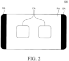
- FIG. 2 is a diagram illustrating a display device 100 according to an embodiment of the present disclosure.
- the display device 100 has central areas CA where the user's eyes are actually located when the display device 100 is fixed in front of the user's eyes and dark areas DA which cannot be recognized by the user who may see only a part of a peripheral area PA on both sides thereof. Further, a distance between the display device 100 and the user's eyes is decreased as compared with a case of using the display device 100 for normal use. Therefore, the user can more easily recognize the resolution of the display device 100.
- pixels in the central areas CA should not have a dark spot or a bright spot and pixels in the peripheral area PA should have an image quality equivalent to or similar to an image displayed when the display device 100 is used for normal use.
- a display area of the display device 100 needs to be managed or controlled separately.
- a black screen can be implemented by turning off pixels in the dark areas DA in order for the dark areas DA not to be displayed on a screen. Since a partial area of the display device 100 is actually not driven, power consumption can be reduced and the screen can be driven at a higher speed.
- the display device 100 needs a driving speed of about 60 Hz for normal use and a driving speed of about 75 Hz or more for implementing VR. As a driving speed is increased, moving images are overlapped due to an image sticking effect and blurring of the moving images is worsened. Therefore, by reducing a persistence time of the images on the screen, it is possible to minimize the overlaps of the images and make the user recognize as if a response speed is high.
- the display device 100 has a persistence time of 16 ms at the time of driving at 60 Hz but has a short persistence time of 2 ms at the time of driving at 75 Hz or more, so that it is possible to suppress motion blur. This may be referred to as "Low Persistency (LP)". In the following, a method using this will be referred to as an LP mode, a VR mode, or a partial driving mode.
- LP Low Persistency
- an organic light emitting panel is used in the display device 100 for implementing the partial driving mode.
- a driving speed is increased, a display time of a frame on a screen is decreased and a driving time of each pixel is also decreased. Therefore, a pixel compensation time may not be sufficient. Accordingly, a necessary part of the screen may be driven and an unnecessary part may not be driven, so that a pixel compensation time can be secured.
- a pixel compensation time substantially equivalent to that for implementing a normal driving speed of 60 Hz can be maintained.
- the display device 100 may be operated in a normal driving mode.
- the display device 100 may be operated in the partial driving mode. In order to increase a driving speed and reduce a persistence time in the partial driving mode, the pixels in the dark areas DA are turned off, so that the screen can be readily driven at a high speed.
- the display device for implementing VR has been described in the embodiments of the present disclosure, they can also be applied to a display device for implementing augmented reality (AR) or mixed reality (MR).
- AR augmented reality
- MR mixed reality
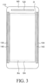
- FIG. 3 is a diagram illustrating a display panel according to an embodiment of the present disclosure.
- the display panel illustrated in FIG. 3 may be used.
- the display panel includes a substrate 110 divided into a display area D where a plurality of pixels are disposed to display an image and a non-display area ND where an image is not displayed.
- a non-display area ND surrounding the display area D, dummy pixels which do not emit lights may be disposed.
- the plurality of pixels disposed in the display area D operate upon receipt of a data signal and a gate signal through a data line and a gate line, respectively.
- the data line may be applied with a signal as being connected to a data driver 120 disposed at an upper portion of the substrate 110.
- the data driver 120 may be manufactured in the form of a driver-ic and then attached on the substrate 110. However, a position or shape of the data driver 120 is not limited thereto.
- the gate lines may include an emission line that controls a gate electrode of a transistor configured to control emission of pixels.
- the emission line may be applied with an emission signal as being connected to an emission driver 140.
- the gate lines may include a scan line that controls a gate electrode of a switching transistor configured to switch a signal unlike the transistor configured to control emission of pixels.
- the scan line may be applied with a scan signal as being connected to a scan driver 130.
- the scan driver 130 and the emission driver 140 are commonly referred to as a gate driver.
- the gate driver may be a GIP circuit directly formed on the substrate 110.
- the gate driver may be symmetrically designed on both sides, but is not limited thereto. Further, the gate driver may refer to the scan driver 130.
- the display panel In the partial driving mode for implementing VR, the display panel needs to turn off pixels disposed in a partial area of the display area D.
- the user stares at the display panel illustrated in FIG. 3 in a state of being rotated 90 degrees clockwise or counterclockwise. Therefore, the user cannot recognize some areas of a left side and a right side of the display panel. That is, in the state as illustrated in FIG. 3 , pixels disposed in partial areas of an upper portion and a lower portion of the display panel need to be able to be turned off. Therefore, the dark areas DA may be above and below the peripheral area PA including the central areas CA.
- the dark area DA disposed on an upper portion of the display panel includes some part of the display area D and may be referred to as a first area.
- the dark area DA disposed on a lower portion of the display panel includes some part of the display area D and may be referred to as a third area.
- the peripheral area PA including the central areas CA may be referred to as a second area.
- a gate driver connected to the pixels in the first area and the third area may be controlled not to generate an output signal.
- a gate start pulse voltage (GVST) and a clock signal to be input to the gate driver connected to the first area and the third area may be blocked.
- line mura may be generated at a boundary between the first area and the second area and a boundary between the second area and the third area. While the gate driver connected to the first area and the third area is not driven, a gate driver connected to the second area is driven. Thus, a stress applied to the gate driver connected to the second area is higher than a stress applied to the gate driver connected to the first area and the third area. Therefore, the gate driver connected to the second area deteriorates more than the gate driver connected to the first area and the third area and a delay of an output signal generated from the gate driver connected to the second area is occurred. Accordingly, line mura may be generated at the boundary between the first area and the second area and the boundary between the second area and the third area.
- a method of making the gate driver connected to the peripheral area PA and the gate driver connected to the dark areas DA similar or almost identical in the degree of deterioration may be applied. That is, in the partial driving mode, driving of the gate driver connected to the dark areas DA is not stopped, and while the gate driver connected to the peripheral area PA is driven, the gate driver connected to the dark areas DA is also driven.
- the gate driver includes the scan driver 130 and the emission driver 140.
- a delay of an output signal output from the gate driver is more affected by the degree of deterioration of the scan driver 130 than by the degree of deterioration of the emission driver 140. This is because a turn-on time of a transistor of the scan driver 130 is longer than a turn-on time of a transistor of the emission driver 140 and a difference in voltage applied to the transistor of the scan driver 130 between drain-source, gate-source, or gate-drain is greater than a difference in voltage applied to the transistor of the emission driver 140. Therefore, by blocking the gate start pulse voltage (GVST) and the clock signal in the partial driving mode, the emission driver 140 is controlled not to be driven and the scan driver 130 is controlled to be driven. In this case, since the emission driver 140 is not driven, the pixels in the dark areas DA do not emit light.
- GVST gate start pulse voltage
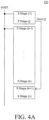
- FIG. 4A is a block diagram illustrating the scan driver 130 according to an embodiment of the present disclosure. There may be various methods of operating the scan driver 130 connected to the dark areas DA while the partial driving mode is executed. FIG. 4A illustrates an embodiment thereof.
- the gate driver includes n number of gate driver stages for sequentially transferring a signal to each pixel row is present.
- the gate driver includes the scan driver 130 and the emission driver 140.
- the scan driver 130 and the emission driver 140 include n number of scan stages S Stages and n number of emission stages, respectively. That is, pixels in each pixel row operate upon receipt of an output signal generated from a gate driver stage connected to each pixel row via a corresponding gate line.
- the scan driver 130 that highly affects a delay of an output signal output from the gate driver as described above will be described.
- a stage is a component included in a driver, and, thus, the concepts of stage and the driver may be interchanged with each other.
- a signal required to operate the scan driver 130 may include a gate clock signal, gate start pulse voltage (GVST), a gate high voltage (VGH), and a gate low voltage (VGL).
- GVST gate start pulse voltage
- VGH gate high voltage
- VGL gate low voltage
- each stage generates an output signal to control driving of pixels disposed in each row.
- a connection relationship between the gate clock signal and the scan stage S Stage will be described later.
- a connection relationship between an input of a signal required to operate the scan stages S Stages connected to the dark areas DA and the scan stages S Stages will be described.
- the scan stages operate in a cascade manner in which each scan stage operates upon receipt of an output signal generated from its previous scan stage. Therefore, pixels disposed after some rows can be turned on by controlling or adjusting a signal to be input to a stage in a row to be turned on first.
- the dark areas DA include the first area where pixels in first to jth (j ⁇ n) pixel rows are disposed and the third area where pixels in (k+1)th to nth pixel rows are disposed.
- the peripheral area PA is the second area where pixels in (j+1)th to kth pixel rows are disposed.
- the pixel rows in the peripheral area PA are between the pixel rows in one dark area DA and the pixel rows in the other dark area DA.
- the total number of the pixel rows in the first area and the third area is smaller than the number of the pixel rows in the second area. That is, (j+n-k) is smaller than (k-j).
- the pixels disposed in the second area are in an on state
- the pixels disposed in the first area and the third area are in an off state.
- Each scan stage is connected to a pixel row through a corresponding scan line.
- a scan line is an example of a gate line.
- Scan stages (1) to (j) are connected to pixel rows (1) to (j) via scan lines (1) to (j).
- Scan stages (j+1) to (k) are connected to pixel rows (j+1) to (k) through scan lines (j+1) to (k).
- Scan stages (k+1) to (n) are connected to pixel rows (k+1) to (n) through scan lines (k+1) to (n).
- GVST gate start pulse voltage
- a (k+1)th scan stage S Stage (k+1) connected to the third area may be driven.
- a signal line may be connected in order for an output signal Gout (j) of the last jth scan stage S Stage (j) connected to the first area to be input to the initial (k+1)th scan stage S Stage (k+1) connected to the third area.
- the scan stages S Stages connected to the first area and the third area can be driven at the same time when the scan stages S Stages connected to the second area are driven.
- FIG. 4B is a graph illustrating a driving sequence of the scan stage S Stage illustrated in FIG. 4A .
- the horizontal axis represents a frame and the vertical axis represents a sequence of scan stages disposed in columns (Column of scan stage). That is, the top in the vertical axis represents the first scan stage S Stage (1) and the bottom in the vertical axis represents an nth scan stage S Stage (n).
- the frame refers to a period in which a gate signal is sequentially applied to all of rows including an area to be displayed on a screen.
- a blank period is present between frames.
- the blank period refers to a period included when any display device is not driven.
- the blank period is present to adjust compatibility between an analog broadcasting signal and a digital display device.
- the blank period may be referred to as a preparatory period for preparing a subsequent frame.
- a signal is simultaneously input to the scan stages connected to the first row and to the scan stages connected to the (j+1)th row and the scan stages are driven.
- a signal is sequentially input to scan stages connected to 1st to jth rows (and so a pulse is sequentially driven to scan lines 1 to j).
- a signal is sequentially input to scan stages connected to (j+1)th to (2j+1)th rows.
- the signal is simultaneously input to a scan stage connected to pixels disposed in a (k+1)th row and also input to a scan stage connected to pixels disposed in a (2j+2)th row.
- a signal is sequentially input to scan stages connected to k+1 to nth rows (and so a pulse is sequentially driven to scan lines k+1 to n). Also during the second period, a signal is sequentially input to scan stages connected to (2j+2)th to (2j+1+n-k)th rows.
- a signal is sequentially input to scan stages connected to (2j+2+n-k) th to kth rows.
- the first period, the second period, and the third period are collectively referred to as a first frame. After finishing the first frame, a blank period is present and then, a second frame is started.
- the first period and the second period refer to periods in which a signal is simultaneously input to two scan stages connected to two rows and then the two scan stages are simultaneously driven.
- the third period refers to a period in which only one scan stage is driven. For example, if a scan stage is driven using one clock signal, the clock signal needs to be input to two scan stages in the first and second periods and input to only one scan stage in the third period. That is, load applied to a clock signal line in the first and second periods is two times higher than load applied to a clock signal line in the third period.
- the delay of the output signal generated from a scan stage occurs between the second period and the third period, and mura may be generated between the second period and the third period.
- two clock signals having the same phase and generated by different amplifiers may be used. A method thereof will be described in detail with reference to FIG. 7 and FIG. 8 .
- FIG. 5A is a block diagram illustrating the scan driver 130 according to another embodiment of the present disclosure.
- FIG. 5A is a modification example of the embodiment illustrated in FIG. 4A . Therefore, a description of the components illustrated in FIG. 4A will be omitted or briefly provided.
- the scan driver 130 illustrated in FIG. 5A further includes a dummy stage in addition to the scan stages illustrated in FIG. 4A .
- the scan driver 130 may include a plurality of dummy stages.
- the dark areas DA of the display panel include the first area where pixels in first to jth (j ⁇ n) rows are disposed and the third area where pixels in (k+1)th to nth rows are disposed.
- the peripheral area PA is the second area where pixels in (j+1)th to kth rows are disposed.
- the total number of the rows in the first area and the third area is smaller than the number of the rows in the second area. That is, (j+n-k) is smaller than (k-j).
- the pixels disposed in the second area are in an on state
- the pixels disposed in the first area and the third area are in an off state.
- Scan stages S Stages connected to the first area and the third area need to be driven while scan stages connected to the second area are driven. That is, a (j+1)th scan stage S Stage (j+1) connected to a (j+1)th row which is a first row in the second area and a first scan stage S Stage (1) connected to a first row in the first area may be driven at the same time.
- the first scan stage S Stage (1) and the (j+1)th scan stage S Stage (j+1) may be connected to the gate start pulse voltage line GVST line to be applied with the gate start pulse voltage (GVST).
- a (k+1)th scan stage S Stage (k+1) connected to the third area may be driven.
- a signal line may be connected in order for an output signal Gout (j) of the jth scan stage S Stage (j) to be input to the (k+1)th scan stage S Stage (k+1).
- the dummy stage when the total number of rows in the first area and third area is different than a number of rows in the second area, the dummy stage is connected to stages for the area having a smaller number of rows (e.g. to the third area in FIG. 5A ). Since the number of the rows included in the first area and the third area is smaller than the number of the rows included in the second area, a third period occurs in which only the scan stages connected to the second area are driven. Thus, a delay of an output signal onto the scan lines may be caused by stresses applied to the scan stages connected to the second area that are driven in the third period. Therefore, scan stages connected to two rows need to be driven in the third period in the same manner as first and second periods in order to adjust a delay time of an output signal. To this end, the dummy stage may be further disposed.
- the dummy stage may be connected to a line in order for an output signal Gout (n) of the last nth scan stage S Stage (n) to be input to a first dummy stage. Also, if there are (a) number of dummy stages, a line 508 may be connected in order for an output signal of an ath dummy stage to be input to a first dummy stage. Thus, the dummy stages may be driven until all of the scan stages connected to the second area are driven.
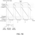
- FIG. 5B is a graph illustrating a driving sequence of the scan stage S Stage illustrated in FIG. 5A and is a modified example of the graph illustrated in FIG. 4B . Therefore, a description of the same components will be omitted or briefly provided.
- the first and a second periods of FIG. 5B are driven in the same manner as the first and second periods of FIG. 4B .
- the dummy stage is repeatedly driven in the third period unlike the third period of FIG. 4B . That is, in all of the first period, the second period, and the third period of FIG. 5B , two scan stages connected to two rows are driven.
- a signal is simultaneously input to the scan stages connected to the first row and the (j+1)th row and the scan stages are driven.
- a signal is sequentially input to scan stages connected to 1st to jth rows.
- a signal is sequentially input to scan stages connected to (j+1)th to (2j+1)th rows.
- a signal is simultaneously input to a scan stage connected to pixels disposed in a (k+1)th row and also input to a scan stage connected to pixels disposed in a (2j+2)th row.
- a signal is sequentially input to scan stages connected to k+1 to nth rows.
- a signal is sequentially input to scan stages connected to (2j+2)th to (2j+1+n-k)th rows.
- the dummy stage is repeatedly driven while the signal is sequentially input to scan stages connected to (2j+2+n-k) th to kth rows
- FIG. 6A is a block diagram illustrating the scan driver 130 according to another embodiment of the present disclosure.
- the scan driver 130 illustrated in FIG. 6A is similar to the scan driver 130 illustrated in FIG. 4A in configuration except a connection relationship between scan stages.
- the dark areas DA of the display panel include the first area where pixels in first to jth (j ⁇ n) rows are disposed and the third area where pixels in (k+1)th to nth rows are disposed.
- the peripheral area PA is the second area where pixels in (j+1)th to kth rows are disposed.
- the total number of the rows in the first area and the third area is smaller than the number of the rows in the second area. That is, (j+n-k) is smaller than (k-j).
- the pixels disposed in the second area are in an on state
- the pixels disposed in the first area and the third area are in an off state.
- Scan stages S Stages connected to the first area and the third area may be driven after scan stages in the second area are driven. That is, a line may be connected in order for an output signal Gout (k) of a kth scan stage S Stage (k) connected to a kth row which is a last row in the second area to be input to all of the scan stages S Stage (1) to S Stage(j) and S Stage (k+1) to S Stage (n) connected to the first area and the third area.
- a first scan stage S Stage (j+1) connected to the second area and all of the scan stages connected to the first area and the third area may be driven.
- the first scan stage S Stage (j+1) in the second area, a first scan stage S Stage (1) to a jth scan stage S Stage (j) in the first area, and a (k+1)th scan stage S Stage (k+1) to an nth scan stage S Stage (n) in the third area may be connected to a gate start pulse voltage line (GVST line) to be applied with the gate start pulse voltage (GVST).
- GVST line gate start pulse voltage line
- scan stages connected to all of the rows in the first area and the third area may be driven at the same time.
- FIG. 6B is a graph illustrating a driving sequence of the scan stage S Stage illustrated in FIG. 6A .
- the scan stages connected to the first area and the third area may be driven in a blank period, which is a preparatory period for preparing a subsequent frame, between each frames.
- a signal is input to the scan stage connected to pixels disposed in the (j+1)th row of the second area and then, the (j+1)th scan stage to the kth scan stage connected to pixels disposed in the kth row are sequentially driven. And, all of the scan stages S Stage (1) to S Stage (j) and S Stage (k+1) to S Stage (n) connected to the first area and the third area may be driven at the same time.
- the scan stages connected to the first area and the third area are not driven while the scan stages connected to the second area, where pixels actually emit light in the partial driving mode, are driven. Instead, the scan stages connected to the first area and third area are driven in the blank period. Thus, the scan stages connected to the first area and the third area do not affect driving of the scan stages connected to the second area. Therefore, it is possible to suppress a delay of an output waveform of a scan stage.
- FIG. 7 is a block diagram illustrating a connection structure of clock signal lines of the scan driver 130 according to an embodiment of the present disclosure.
- the scan driver 130 includes n numbers of scan stages.
- the first area may be connected to j number of scan stages
- the second area may be connected to (k-j) number of scan stages
- the third area may be connected to (n-k) number of scan stages.
- pixels disposed in the second area are in an on state
- pixels disposed in the first area and the third area are in an off state.
- a clock signal to be input to the scan stages includes a clock signal a (Cka) and a clock signal b (Ckb).
- the clock signal a (Cka) and the clock signal b (Ckb) have the same phase and are respectively generated by different amplifiers mounted in an integrated chip (IC) that generates a clock signal.
- each of the clock signal a (Cka) and the clock signal b (Ckb) may be a 2-phase signal.
- the clock signal a (Cka) includes a clock signal a_1 (Cka_1) and a clock signal a_2 (Cka_2).
- the clock signal b (Ckb) includes a clock signal b_1 (Ckb_1) and a clock signal b_2 (Ckb_2).
- the phase of the clock signal is not limited to the 2-phase.
- the scan driver 130 includes a clock signal a line (Cka line) and a clock signal b line (Ckb line) to which the clock signal a (Cka) and the clock signal b (Ckb) may be applied.
- two scan stages connected to two rows are driven in the first period and the second period. That is, while the scan stages connected to the second area are sequentially driven, the scan stages connected to the first area and the third area are sequentially driven.
- the clock signal lines may be connected to the scan stages as shown in FIG. 7 .
- the clock signal line connections prevent clock signals generated by the same amplifier from being applied, in the first period and the second period, to two scan stages that are driven at the same time.
- a clock signal a (Cka_1, Cka_2) line may be connected to each of the j number of scan stages and the (n-k) number of scan stages connected to the first area and the third area.
- a clock signal b (Ckb_1, Ckb_2) line may be connected to the first subset 702 of (j+n-k) number of scan stages in the second area which are driven at the same time as the scan stages connected to the first area and the third area.
- (j+n-k) X a (a is a natural number) equals (k-j).
- the clock signal a (Cka_1, Cka_2) line and the clock signal b (Ckb_1, Ckb_2) line may be alternately connected to subsets 702-708 of scan stages driven in the third period.
- the clock signal a (Cka_1, Cka_2) line and the clock signal b (Ckb_1, Ckb_2) line are alternately connected to subsets 702-708 of scan stages, where each subset of scan stages includes(j+n-k) number of scan stages, but the present disclosure is not limited thereto.
- the clock signal a and the clock signal b may be referred to as a first clock signal and a second clock signal, respectively.
- the clock signal a line and the clock signal b line may be referred to as a first clock signal line and a second clock signal line, respectively.
- a first clock signal is applied to the first clock signal line and a second clock signal is applied to the second clock signal line.
- the second clock signal has the same phase as the first clock signal but is generated by an amplifier different from an amplifier that generates the first clock signal.
- the first clock signal and the second clock signal may be input to respective scan stages that are driven at the same time, so that it is possible to reduce load applied to the first clock signal line and the second clock signal line.
- the scan stages connected to the first area and the third area, and the scan stages connected to the second area may become similar or almost identical in their degree of deterioration.
- FIG. 8 is a block diagram illustrating a connection structure of clock signal lines of the scan driver 130 according to another embodiment of the present disclosure.
- the scan driver 130 includes n numbers of scan stages.
- the first area may be connected to j number of scan stages
- the second area may be connected to (k-j) number of scan stages
- the third area may be connected to (n-k) number of scan stages.
- pixels disposed in the second area are in an on state
- pixels disposed in the first area and the third area are in an off state.
- a clock signal to be input to the scan stages includes a clock signal a (Cka) and a clock signal b (Ckb).
- the clock signal a (Cka) and the clock signal b (Ckb) have the same phase and are respectively generated by different amplifiers mounted in an integrated chip (IC) that generates a clock signal.
- each of the clock signal a (Cka) and the clock signal b (Ckb) may be a 2-phase signal.
- the clock signal a (Cka) includes a clock signal a_1 (Cka_1) and a clock signal a_2 (Cka_2).
- the clock signal b (Ckb) includes a clock signal b_1 (Ckb_1) and a clock signal b_2 (Ckb_2).
- the clock signal may have more than and fewer than two phases.
- the scan driver 130 includes a clock signal a line (Cka line) and a clock signal b line (Ckb line) to which the clock signal a (Cka) and the clock signal b (Ckb) may be applied.
- the clock signal lines may be connected to the scan stages so that the same clock signal is not applied, in the first and second periods, to two scan stages that are driven at the same time. That is, two scan stages to be driven at the same time are not connected to the same clock signal line, so that load is not increased. Thus, an output signal may not be delayed.
- clock signal lines are closely distributed in each scan stage as compared with the embodiment in FIG. 7 .
- load applied to the clock signal lines can be precisely divided or distributed.
- the clock signal a (Cka_1, Cka_2) line and the clock signal b (Ckb_1, Ckb_2) line may be alternately connected in sequence to subsets of two scan stages of the j number of scan stages connected to the first area, and alternately connected to subsets of (n-k) number of scan stages connected to the third area.
- the clock signal b (Ckb_1, Ckb_2) line and the clock signal a (Cka_1, Cka_2) line may be alternately connected in sequence to subsets of two scan stages of the (k-j) number of scan stages connected to the second area.
- the connections between the scan stages and the clock signal a line and the clock signal b line may alternate with each individual scan stage. More generically, the clock signal a line and the clock signal b line may be alternately connected to subsets of scan stages that have fewer than than (j+n-k) scan stages per subset, wherein j+n-k is the total number of the rows included in the first area and the third area.
- different clock signal lines i.e., the clock signal a line and the clock signal b line
- the clock signal a and the clock signal b may be referred to as a first clock signal and a second clock signal, respectively.
- the clock signal a line and the clock signal b line may be referred to as a first clock signal line and a second clock signal line, respectively.
- the first clock signal line and the second clock signal line which are connected to the scan stages connected to the pixels disposed in the first and third areas and the scan stages connected to the pixels disposed in the second area, are alternately connected to m (m is a natural number) number of rows.
- m is a natural number
- by adjusting load it is possible to suppress a delay of an output waveform of a scan stage caused by a difference in load. Therefore, it is possible to suppress the generation of line mura at the boundary between the first area and the second area and the boundary between the second area and the third area at the time of switch from the partial driving mode to the normal driving mode.
- a display panel comprising a substrate including a first area and a second area, a gate driver configured to supply a gate signal to pixels disposed on the substrate, the gate driver having a a plurality of stages, and a first clock signal line and a second clock signal line to be respectively applied with a first clock signal and a second clock signal having a same phase.
- the plurality of stages are connected to the first area and the second area and driven at the same time.
- the first clock signal line and the second clock signal line are connected to each of the plurality of stages connected to the first area and the second area.
- the stages connected to the first area and the second area become similar or almost identical in the degree of deterioration. And, it is possible to suppress the generation of line mura at a boundary between the first area and the second area at the time of switch from a partial driving mode to a normal driving mode.
- the pixels in the first area of the display panel may be in an off state and the pixels in the second area may be in an on state.
- the gate driver may include an emission driver and a scan driver.
- the plurality of stages may constitute the scan driver.
- the plurality of stages connected to the pixels in the first area may be connected to the first clock signal line and the plurality of stages connected to the pixels in the second area may be connected to the second clock signal line.
- the second area of the display panel may further include a plurality of stages connected to the first clock signal line.
- the gate driver may include an emission driver and a scan driver.
- the plurality of stages may constitute the scan driver.
- the first clock signal line and the second clock signal line respectively connected to the plurality of stages connected to the pixels in the first area and a plurality of stages connected to the pixels in the second area may be alternately connected to every m (m ⁇ (j + n - k), j ⁇ k ⁇ n, where j, k, m and n are natural numbers) number of rows.
- the substrate may further include a third area.
- the pixels in the first area and the third area may be in an off state and pixels in the second area may be in an on state.
- the gate driver may include an emission driver and a scan driver.
- the plurality of stages may constitute the scan driver.
- the plurality of stages connected to the pixels in the first area and the third area may be connected to the first clock signal line and the plurality of stages connected to the pixels in the second area may be connected to the second clock signal line.
- a line may be connected to provide an output signal of a stage connected to pixels in a last row of the first area of the display panel to be input to a stage connected to pixels in a first row of the third area.
- the second area of the display panel may further include a plurality of stages connected to the first clock signal line.
- the gate driver may include an emission driver and a scan driver.
- the plurality of stages may constitute the scan driver.
- the first clock signal line and the second clock signal line respectively connected to a plurality of stages connected to the pixels in the first area and the third area and the plurality of stages connected to the pixels in the second area may be alternately connected to every m (m ⁇ (j + n - k), j ⁇ k ⁇ n, where j, k, m and n are natural numbers) number of rows.
- the gate driver may further include a dummy stage.
- a dummy stage may be connected to a stage connected to an area of a smaller number of rows among the first area and the second area.
- a load applied to the first clock signal line and a load applied to the second clock signal line may be identical to each other.
- a display panel comprising a substrate including a first area and a second area, a gate driver configured to supply a gate signal to pixels disposed on the substrate, the gate driver comprising a plurality of stages, and a first clock signal line configured to apply a first clock signal and a second clock signal line configured to apply a second clock signal to the gate driver. While pixels in the first area are in an off state, the first clock signal line is connected to one or more stages of the plurality of stages connected to the pixels, the one or more stages connected to the pixels in the first area.
- the gate drivers connected to the first area and the second area become similar or almost identical in the degree of deterioration. Also, it is possible to suppress the generation of line mura at a boundary between the first area and the second area at the time of switch from a partial driving mode to a normal driving mode.
- the pixels in the second area of the display panel may be in an on state.
- the first clock signal and the second clock signal may be respectively generated by different amplifiers and may have a same phase.
- the first area of the display panel may include j (j is natural number) number of rows and the second area may include more than j number of rows.
- the plurality of stages connected to pixels in a first row to a jth row in the second area may be connected to the second clock signal line.
- the first clock signal and the second clock signal may be simultaneously input to each of the plurality of stages connected to the pixels in the first area and the plurality of stages connected to pixels in the second area.
- the gate driver may further include a dummy stage.
- the dummy stage may be connected to a stage connected to an area of a smaller number of rows among the first area and the second area.
- a line may be connected to provide an output signal of a stage connected to pixels in a last row of the second area of the display panel to be input to a stage connected to pixels in a first row of the first area.
- a load applied to the first clock signal line and a load applied to the second clock signal line may be identical to each other.
- a display panel comprises a plurality of first pixel rows, a plurality of second pixel rows, a first clock signal line to carry a first clock signal, and a second clock signal line to carry a second clock signal that is in phase with the first clock signal.
- a gate driver includes a plurality of first gate driver stages connected to the plurality of first pixel rows, and a plurality of second gate driver stages connected to the plurality of second pixel rows.
- a first gate driver stage of the plurality of first gate driver stages is driven at a same time as a second gate driver stage of the plurality of second gate driver stages.
- the first gate driver stage is connected to the first clock signal line and the second gate driver stage is connected to the second clock signal line.
- a display panel may further comprise a plurality of third pixel rows.
- the gate driver may comprise a plurality of third gate driver stages connected to the plurality of third pixel rows.
- a third gate driver stage of the plurality of third gate driver stages may be driven at a same time as an additional second gate driver stage of the plurality of second gate driver stages.
- the third gate driver stage may be connected to the first clock signal line.
- the second pixel rows may be between the first pixel rows and the third pixel rows.
- the display panel may further include a signal line to provide an output signal of a last gate driver stage of the plurality of first gate driver stages to an input of an initial gate driver stage of the plurality of third gate driver stages.
- the gate driver may further include a dummy driver stage and a signal line to provide an output signal of a last gate driver stage of the plurality of third gate driver stages to an input of the dummy driver stage.
- the plurality of first gate driver stages may be driven sequentially.
- the plurality of second gate driver stages may be driven sequentially at a same time as the plurality of first gate driver stages.
- the plurality of first gate driver stages may be connected to the first clock signal line and the plurality of second gate driver stages are connected to the second clock signal line.
- the plurality of first gate driver stages may include 1 st to jth gate driver stages.
- the plurality of second gate driver stages may include at least a j+1th gate driver stage.
- the plurality of first gate driver stages may be driven sequentially.
- the plurality of second gate driver stages may be driven sequentially at a same time as the plurality of first gate driver stages being driven sequentially.
- Subsets of the plurality of first gate driver stages may be connected in alternating manner to the first clock signal line and the second clock signal line.
- Subsets of the plurality of second gate driver stages may be connected in alternating manner to the second clock signal line and the first clock signal line.
- a load applied to the first clock signal line and a load applied to the second clock signal line may be identical to each other.
- the gate driver may be a scan driver.
- pixels in the first pixel rows may be in an off state and pixels in the second pixels rows are in an on state.
- a display panel comprises a plurality of first pixel rows corresponding to a plurality of first gate lines.
- a plurality of second pixel rows correspond to a plurality of second gate lines.
- a gate driver has a plurality of first gate driver stages connected to the plurality of first gate lines and a plurality of second gate driver stages connected to the plurality of second gate lines. The plurality of second gate driver stages are driven sequentially, and all first gate driver stages of the plurality of first gate driver stages are driven at the same time.
- the display panel may comprise a plurality of third pixel rows corresponding to a plurality of third gate lines.
- the gate driver may comprise a plurality of third gate driver stages connected to the plurality of third pixel rows via the plurality of third gate lines. All first gate driver stages of the plurality of first gate driver stages and all third gate driver stages of the plurality of third gate driver stages may be driven at a same time.
- the plurality of first gate driver stages may be driven in a blank period.
- a signal line may provide an output signal of a last gate driver stage of the plurality of second gate driver stages to inputs of each first gate driver stage of the plurality of first gate driver stages.
- a display panel comprises a substrate including a first area and a second area, a gate driver configured to supply a gate signal to pixels disposed on the substrate, the gate driver having a plurality of stages, and a first clock signal line and a second clock signal line to be respectively applied with a first clock signal and a second clock signal having a same phase, wherein the plurality of stages are connected to the first area and the second area and driven at the same time, and the first clock signal line and the second clock signal line are connected to each of the plurality of stages connected to the first area and the second area.
- the pixels in the first area may be in an off state and/or the pixels in the second area may be in an on state.
- the gate driver may include an emission driver and a scan driver.
- the plurality of stages may constitute the scan driver.
- the plurality of stages connected to the pixels in the first area may be connected to the first clock signal line.
- the plurality of stages connected to the pixels in the second area may be connected to the second clock signal line.
- the second area may further include a plurality of stages connected to the first clock signal line.
- the gate driver may include an emission driver and a scan driver.
- the plurality of stages may constitute the scan driver.
- the first clock signal line and the second clock signal line respectively connected to the plurality of stages connected to the pixels in the first area and the plurality of stages connected to the pixels in the second area may be alternately connected to every m (m ⁇ (j + n - k), j ⁇ k ⁇ n, where j, k, m and n are natural numbers) number of rows.
- the substrate may further include a third area, and the pixels in the first area and the third area are in an off state and pixels in the second area are in an on state.
- the gate driver may include an emission driver and a scan driver.
- the plurality of stages may constitute the scan driver.
- the plurality of stages connected to the pixels in the first area and the third area may be connected to the first clock signal line.
- the plurality of stages connected to the pixels in the second area may be connected to the second clock signal line.
- a line may be connected to provide an output signal of a stage connected to pixels in a last row of the first area to be input to a stage connected to pixels in a first row of the third area.
- the second area may further include a plurality of stages connected to the first clock signal line.
- the gate driver may include an emission driver and a scan driver.
- the plurality of stages may constitute the scan driver.
- the first clock signal line and the second clock signal line respectively connected to a plurality of stages connected to the pixels in the first area and the third area and the plurality of stages connected to the pixels in the second area may be alternately connected to every m (m ⁇ (j + n - k), j ⁇ k ⁇ n, where j, k, m and n are natural numbers) number of rows.
- the gate driver may further include a dummy stage connected to a stage connected to an area of a smaller number of rows among the first area and the second area.
- a load applied to the first clock signal line and a load applied to the second clock signal line may be identical to each other.
- a display panel comprises a substrate including a first area and a second area, a gate driver configured to supply a gate signal to pixels disposed on the substrate, the gate driver comprising a plurality of stages, and a first clock signal line configured to apply a first clock signal to the gate driver and a second clock signal line configured to apply a second clock signal to the gate driver, wherein while pixels in the first area are in an off state, the first clock signal line is connected to one or more stages of the plurality of stages, the one or more stages connected to the pixels in the first area.
- the pixels in the second area may be in an on state.
- the first clock signal and the second clock signal may be respectively generated by different amplifiers and have a same phase.
- the first area may include j (j is natural number) number of rows and the second area may include more than j number of rows.
- the plurality of stages connected to pixels in a first row to a jth row in the second area may be connected to the second clock signal line.
- the first clock signal and the second clock signal may be simultaneously input to each of the plurality of stages connected to the pixels in the first area and the plurality of stages connected to pixels in the second area.
- the gate driver may further include a dummy stage.
- the dummy stage may be connected to a stage connected to an area of a smaller number of rows among the first area and the second area.
- a load applied to the first clock signal line and a load applied to the second clock signal line may be identical to each other.
- a display panel comprises a plurality of first pixel rows; a plurality of second pixel rows, a first clock signal line to carry a first clock signal, a second clock signal line to carry a second clock signal that is in phase with the first clock signal, and a gate driver having a plurality of first gate driver stages connected to the plurality of first pixel rows and a plurality of second gate driver stages connected to the plurality of second pixel rows, wherein a first gate driver stage of the first gate driver stages is driven at a same time as a second gate driver stage of the plurality of gate driver stages, wherein the first gate driver stage is connected to the first clock signal line and wherein the second gate driver stage is connected to the second clock signal line.
- the display panel may further comprise a plurality of third pixel rows; wherein the gate driver comprises a plurality of third gate driver stages connected to the plurality of third pixel rows, wherein a third gate driver stage of the third gate driver stages is driven at a same time as an additional second gate driver stage of the plurality of second gate driver stages, and wherein the third gate driver stage is connected to the first clock signal line.
- the second pixel rows may be between the first pixel rows and the third pixel rows.
- the display panel may further comprise a signal line to provide an output signal of a last gate driver stage of the first gate driver stages to an input of an initial gate driver stage of the third gate driver stages.
- the gate driver may further include a dummy driver stage; and a signal line to provide an output signal of a last gate driver stage of the third gate driver stages to an input of the dummy driver stage.
- the plurality of first gate driver stages may be driven sequentially.
- the plurality of second gate driver stages may be driven sequentially at a same time as the first gate driver stages.
- the first gate driver stages may be connected to the first clock signal line and the second gate driver stages may be connected to the second clock signal line.
- the plurality of first gate driver stages may include 1 st to jth gate driver stages.
- the plurality of second gate driver stages may include at least a j+1th gate driver stage.
- the plurality of first gate driver stages may be driven sequentially.
- the plurality of second gate driver stages may be driven sequentially, the first gate driver stages being driven sequentially at a same time as the second gate driver stages being driven sequentially.
- Subsets of the first gate driver stages may be connected in alternating manner to the first clock signal line and the second clock signal line.
- Subsets of the second gate driver stages may be connected in alterating manner to the second clock signal line and the first clock signal line.
- a load applied to the first clock signal line and a load applied to the second clock signal line may be identical to each other.
- the gate driver may be a scan driver.
- pixels in the first pixel rows may be in an off state and pixels in the second pixels rows may be in an on state.
- a display panel comprises a substrate including a plurality of pixels arranged in a first area and in a second area, a gate driver configured to supply a gate signal to the pixels, the gate driver including at least one first stage connected to the pixels in the first area and at least one second stage connected to the pixels in the second area, a first clock signal line connected to the first stage for providing a first clock signal, and a second clock signal line connected to the second stage for providing a second clock signal.
- the second clock signal may have the same phase as the first clock signal.
- the first stage connected to pixels in the first area and the second stage connected to pixels in the second area may be configured to be driven at the same time.
- the gate driver may include an emission driver and a scan driver, the scan driver comprising the plurality of first and second stages.
- the first clock signal line and the second clock signal line may be alternately connected to m number of rows, with m ⁇ j, j ⁇ n, j, m and n are natural numbers, j is the number of stages in the first area and n is the total number of stages.
- the substrate may further include a third area, and the pixels in the first area and the third area may be in an off state and pixels in the second area are in an on state.
- the gate driver may include a plurality of third stages connected to the pixels in the third area, the third stages being connected to the first clock signal line.
- An output of a stage connected to pixels in a last row of the first area may be connected to an input of a stage connected to pixels in a first row of the third area.
- the first clock signal line and the second clock signal line may be alternately connected to m number of rows, with m ⁇ (j + n - k), j ⁇ k ⁇ n, j, k, m and n are natural numbers, j is the number of stages in the first area, k is the number of stages in the second area and n is the total number of stages.
- the gate driver may further include a dummy stage, and the dummy stage may be connected to a stage connected to an area having a smaller number of rows among the first area and the second area.
- a load applied to the first clock signal line and a load applied to the second clock signal line may be identical to each other.
- the first clock signal and the second clock signal may be respectively generated by different amplifiers and may have a same phase.
- the first area may include j rows, with j being a natural number
- the second area may include (k-j) rows, with k being a natural number and larger than j
- the plurality of stages connected to pixels in a (j+1)th row to a (2j+1)th row in the second area may be connected to the second clock signal line.
- An output of a stage connected to pixels in a last row of the second area may be connected to an input of a stage connected to pixels in a first row of the first area.
- a method for driving a display panel having a substrate including a plurality of pixels arranged in a first area and in a second area, a gate driver including at least one first stage connected to the pixels in the first area and at least one second stage connected to the pixels in the second area, a first clock signal line connected to the first stage for providing a first clock signal, and a second clock signal line connected to the second stage for providing a second clock signal, the method comprising: supplying a gate signal to the pixels, and supplying a first clock signal to the first stage and a second clock signal to the second stage, wherein the second clock signal has the same phase as the first clock signal and wherein the first stage connected to pixels in the first area and the second stage connected to pixels in the second area are driven at the same time.
- the first clock signal and the second clock signal may be simultaneously input to the plurality of stages connected to the pixels in the first area and the plurality of stages connected to pixels in the second area.
Landscapes
- Engineering & Computer Science (AREA)
- Theoretical Computer Science (AREA)
- Physics & Mathematics (AREA)
- General Physics & Mathematics (AREA)
- Computer Hardware Design (AREA)
- Chemical & Material Sciences (AREA)
- Crystallography & Structural Chemistry (AREA)
- Human Computer Interaction (AREA)
- General Engineering & Computer Science (AREA)
- Control Of Indicators Other Than Cathode Ray Tubes (AREA)
Claims (10)
- Anzeigetafel (100), die umfasst:ein Substrat (110), das mehrere Pixel enthält, die in einem ersten Bereich (DA) und in einem zweiten Bereich (CA, PA) angeordnet sind;eine Gate-Ansteuerung (130, 140), die konfiguriert ist, ein Gate-Signal an die Pixel zu liefern, wobei die Gate-Ansteuerung (130, 140) mindestens eine erste Stufe, die mit den Pixeln in dem ersten Bereich verbunden ist, und mindestens eine zweite Stufe, die mit den Pixeln in dem zweiten Bereich verbunden ist, enthält;mindestens einen Verstärker, der konfiguriert ist, ein erstes Taktsignal (Cka) und ein zweites Taktsignal (Ckb) zu erzeugen, wobei das zweite Taktsignal (Ckb) dieselbe Phase wie das erste Taktsignal (Cka) besitzt,eine erste Taktsignalleitung, die mit der ersten Stufe verbunden ist, um das erste Taktsignal (Cka) zu liefern; undeine zweite Taktsignalleitung, die mit der zweiten Stufe verbunden ist, um das zweite Taktsignal (Ckb) zu liefern,wobei die Gate-Ansteuerung (130, 140) eine Emissionsansteuerung (140) und eine Abtastansteuerung (130) enthält, wobei die Abtastansteuerung (130) die erste und die zweite Stufe umfasst, wobei die Emissionsansteuerung (140) Emissionsstufen umfasst, die mit den Pixeln in dem ersten und dem zweiten Bereich verbunden sind,wobei die Anzeigetafel (100) konfiguriert ist, entweder in einer normalen Ansteuerungsbetriebsart oder in einer Teilansteuerungsbetriebsart angesteuert zu werden, wobei in der Teilansteuerungsbetriebsart die Pixel in dem ersten Bereich (DA) durch die Emissionsstufen der Emissionsansteuerung (140), die mit den Pixeln in dem ersten Bereich (DA) verbunden ist, so gesteuert werden, dass sie in einem Aus-Zustand sind, und wobei die Pixel in dem zweiten Bereich (CA, PA) durch die Emissionsstufen der Emissionsansteuerung (140), die mit den Pixeln in dem zweiten Bereich (CA, PA) verbunden ist, so gesteuert werden, dass sie in einem Ein-Zustand sind,wobei die erste Stufe der Abtastansteuerung, die mit Pixeln in dem ersten Bereich (DA) verbunden ist, und die zweite Stufe der Abtastansteuerung, die mit den Pixeln in dem zweiten Bereich (CA, PA) verbunden ist, konfiguriert sind, in der Teilansteuerungsbetriebsart zur selben Zeit angesteuert zu werden.
- Anzeigetafel (100) nach Anspruch 1, wobei die erste Taktsignalleitung und die zweite Taktsignalleitung abwechselnd mit einer Anzahl von m Reihen verbunden sind, wobei m ≤ j, j < n, j, m und n natürliche Zahlen sind, j die Anzahl von Stufen in dem ersten Bereich ist und n die Gesamtanzahl von Stufen ist.
- Anzeigetafel (100) nach einem der vorhergehenden Ansprüche, wobei das Substrat (110) ferner einen dritten Bereich (DA) enthält und in der Teilansteuerungsbetriebsart die Pixel in dem ersten Bereich (DA) und dem dritten Bereich (DA) durch die Emissionsstufen der Emissionsansteuerung (140), die mit den Pixeln in dem ersten Bereich (DA) und dem dritten Bereich (DA) verbunden ist, so gesteuert werden, dass sie in einem Aus-Zustand sind, und die Pixel in dem zweiten Bereich (CA, PA) durch die Emissionsstufen der Emissionsansteuerung (140), die mit den Pixeln in dem zweiten Bereich (CA, PA) verbunden ist, so gesteuert werden, dass sie in einem Ein-Zustand sind.
- Anzeigetafel (100) nach Anspruch 3, wobei die Gate-Ansteuerung (130, 140) mehrere dritte Stufen enthält, die mit den Pixeln in dem dritten Bereich (DA) verbunden sind, wobei die dritten Stufen mit der ersten Taktsignalleitung verbunden sind.
- Anzeigetafel (100) nach einem der Ansprüche 3 oder 4, wobei eine Ausgabe einer Stufe, die mit Pixeln in einer letzten Reihe des ersten Bereichs (DA) verbunden ist, mit einem Eingang einer Stufe, die mit Pixeln in einer ersten Reihe des dritten Bereichs (DA) verbunden ist, verbunden ist.
- Anzeigetafel (100) nach Anspruch 1, wobei die erste Taktsignalleitung und die zweite Taktsignalleitung abwechselnd mit einer Anzahl von m Reihen verbunden sind, wobei m ≤ (j + n - k), j < k < n, j, k, m und n natürliche Zahlen sind, j die Anzahl von Stufen in dem ersten Bereich ist, k die Anzahl von Stufen in dem zweiten Bereich (CA, PA) ist und n die Gesamtanzahl von Stufen ist.
- Anzeigetafel (100) nach einem der vorhergehenden Ansprüche, die ferner Verstärker umfasst, um das erste Taktsignal (Cka) und das zweite Taktsignal (Ckb) zu erzeugen, wobei das erste Taktsignal (Cka) und das zweite Taktsignal (Ckb) jeweils durch verschiedene Verstärker erzeugt werden.
- Anzeigetafel (100) nach einem der vorhergehenden Ansprüche, wobei der erste Bereich (DA) j Reihen enthält, wobei j eine natürliche Zahl ist, und der zweite Bereich (CA, PA) (k - j) Reihen enthält, wobei k eine natürliche Zahl und größer als j ist, und die mehreren Stufen, die mit Pixeln in einer (j + 1)-ten Reihe bis zu einer (2j + 1)-ten Reihe in dem zweiten Bereich (CA, PA) verbunden sind, mit der zweiten Taktsignalleitung verbunden sind.
- Anzeigetafel (100) nach einem der vorhergehenden Ansprüche, wobei ein Ausgang einer Stufe, die mit Pixeln in einer letzten Reihe des zweiten Bereichs (CA, PA) verbunden ist, mit einem Eingang einer Stufe, die mit Pixeln in einer ersten Reihe des ersten Bereichs (DA) verbunden ist, verbunden ist.
- Verfahren zur Ansteuerung einer Anzeigetafel (100) nach einem der vorhergehenden Ansprüche, das Folgendes umfasst:Liefern eines Gate-Signals an die Pixel undLiefern eines ersten Taktsignals (Cka) an die erste Stufe der Gate-Ansteuerung und eines zweiten Taktsignals (Ckb) an die zweite Stufe der Gate-Ansteuerung,wobei das zweite Taktsignal (Ckb) dieselbe Phase wie das erste Taktsignal (Cka) besitzt und wobei die erste Stufe der Abtastansteuerung, die mit Pixeln in dem ersten Bereich (DA) verbunden ist, und die zweite Stufe der Abtastansteuerung, die mit Pixeln in dem zweiten Bereich (CA, PA) verbunden ist, zur selben Zeit in einer Teilansteuerungsbetriebsart angesteuert werden, in der die Pixel in dem ersten Bereich (DA) durch die Emissionsstufen der Emissionsansteuerung (140), die mit den Pixeln in dem ersten Bereich (DA) verbunden ist, so gesteuert werden, dass sie in einem Aus-Zustand sind, und die Pixel in dem zweiten Bereich (CA, PA) durch die Emissionsstufen der Emissionsansteuerung (140), die mit den Pixeln in dem zweiten Bereich (CA, PA) verbunden ist, so gesteuert werden, dass sie in einem Ein-Zustand sind.
Applications Claiming Priority (1)
| Application Number | Priority Date | Filing Date | Title |
|---|---|---|---|
| KR1020160182506A KR102924769B1 (ko) | 2016-12-29 | 2016-12-29 | 게이트 구동회로를 포함하는 표시패널 |
Publications (2)
| Publication Number | Publication Date |
|---|---|
| EP3343545A1 EP3343545A1 (de) | 2018-07-04 |
| EP3343545B1 true EP3343545B1 (de) | 2023-05-03 |
Family
ID=59387981
Family Applications (1)
| Application Number | Title | Priority Date | Filing Date |
|---|---|---|---|
| EP17182793.4A Active EP3343545B1 (de) | 2016-12-29 | 2017-07-24 | Anzeigetafel mit gate-treiber und verfahren zur steuerung eines gate-treibers |
Country Status (4)
| Country | Link |
|---|---|
| US (1) | US10424252B2 (de) |
| EP (1) | EP3343545B1 (de) |
| KR (1) | KR102924769B1 (de) |
| CN (1) | CN108257559B (de) |
Families Citing this family (19)
| Publication number | Priority date | Publication date | Assignee | Title |
|---|---|---|---|---|
| KR102709910B1 (ko) | 2016-12-07 | 2024-09-27 | 삼성디스플레이 주식회사 | 표시장치 및 그의 구동방법 |
| KR102740962B1 (ko) | 2017-01-10 | 2024-12-12 | 삼성디스플레이 주식회사 | 표시 장치 및 그의 구동 방법 |
| KR102736801B1 (ko) * | 2017-01-10 | 2024-12-04 | 삼성디스플레이 주식회사 | 표시 장치 및 그의 구동 방법 |
| US10796642B2 (en) * | 2017-01-11 | 2020-10-06 | Samsung Display Co., Ltd. | Display device |
| CN108461067B (zh) * | 2017-02-20 | 2020-09-01 | 元太科技工业股份有限公司 | 电子纸显示器以及电子纸显示面板的驱动方法 |
| JP6872795B2 (ja) * | 2017-10-05 | 2021-05-19 | 株式会社Joled | 表示装置 |
| KR102458254B1 (ko) * | 2018-04-17 | 2022-10-26 | 삼성디스플레이 주식회사 | 표시 장치 |
| CN109064976A (zh) * | 2018-11-01 | 2018-12-21 | 京东方科技集团股份有限公司 | 显示面板的驱动方法、驱动电路及显示装置 |
| KR102748386B1 (ko) * | 2019-04-18 | 2025-01-02 | 삼성디스플레이 주식회사 | 화소 구동 장치 및 이를 포함하는 표시 장치 |
| CN112017570B (zh) | 2019-05-31 | 2022-08-19 | 京东方科技集团股份有限公司 | 栅极驱动电路、显示装置及显示控制方法 |
| KR102752455B1 (ko) * | 2019-09-09 | 2025-01-09 | 삼성디스플레이 주식회사 | 스캔 신호 구동부와 그를 포함한 표시 장치 |
| CN111488859B (zh) * | 2020-05-06 | 2023-06-06 | 武汉华星光电技术有限公司 | 指纹识别驱动电路 |
| US11657756B2 (en) | 2020-10-23 | 2023-05-23 | Chengdu Boe Optoelectronics Technology Co., Ltd. | Display panel and display apparatus |
| CN116490914A (zh) * | 2020-10-30 | 2023-07-25 | 株式会社半导体能源研究所 | 半导体装置、显示装置以及电子设备 |
| KR102772565B1 (ko) * | 2020-11-03 | 2025-02-25 | 엘지디스플레이 주식회사 | 표시패널과 이를 이용한 표시장치 |
| CN112885299B (zh) * | 2021-01-22 | 2022-06-24 | 合肥京东方卓印科技有限公司 | 显示亮度补偿方法、补偿电路、显示装置 |
| US12550551B2 (en) * | 2021-12-29 | 2026-02-10 | Chengdu Boe Optoelectronics Technology Co., Ltd. | Display panel and display device |
| CN114927095A (zh) * | 2022-05-25 | 2022-08-19 | 武汉天马微电子有限公司 | 像素电路及其驱动方法、显示面板 |
| CN115985264A (zh) * | 2023-01-09 | 2023-04-18 | 合肥京东方显示技术有限公司 | 一种显示面板及显示装置 |
Citations (3)
| Publication number | Priority date | Publication date | Assignee | Title |
|---|---|---|---|---|
| GB2452278A (en) * | 2007-08-30 | 2009-03-04 | Sharp Kk | A scan pulse shift register for an active matrix LCD display |
| EP2186097A1 (de) * | 2007-08-30 | 2010-05-19 | Sharp Kabushiki Kaisha | Schieberegister, anzeigetreiber und display |
| KR20160083791A (ko) * | 2014-12-30 | 2016-07-12 | 엘지디스플레이 주식회사 | 터치 센서들을 가지는 표시장치와 그 게이트 구동 회로 |
Family Cites Families (9)
| Publication number | Priority date | Publication date | Assignee | Title |
|---|---|---|---|---|
| TW200600916A (en) * | 2004-05-27 | 2006-01-01 | Alps Electric Co Ltd | Color liquid crystal display device |
| KR101871188B1 (ko) * | 2011-02-17 | 2018-06-28 | 삼성디스플레이 주식회사 | 유기전계발광 표시장치 및 그의 구동방법 |
| WO2012156942A1 (en) * | 2011-05-17 | 2012-11-22 | Ignis Innovation Inc. | Systems and methods for display systems with dynamic power control |
| US9606607B2 (en) * | 2011-05-17 | 2017-03-28 | Ignis Innovation Inc. | Systems and methods for display systems with dynamic power control |
| KR101850990B1 (ko) * | 2011-07-06 | 2018-04-23 | 삼성디스플레이 주식회사 | 표시 장치 및 그 구동 방법 |
| US9646559B2 (en) * | 2012-08-10 | 2017-05-09 | Lg Display Co., Ltd. | Liquid crystal display device |
| KR102139693B1 (ko) * | 2013-11-18 | 2020-07-31 | 삼성디스플레이 주식회사 | 휘도 제어 방법, 휘도 제어 유닛 및 이를 구비하는 유기 발광 표시 장치 |
| CN103943084A (zh) * | 2014-04-01 | 2014-07-23 | 京东方科技集团股份有限公司 | 一种显示面板、显示面板驱动方法及3d显示设备 |
| KR102586792B1 (ko) * | 2016-08-23 | 2023-10-12 | 삼성디스플레이 주식회사 | 표시장치 및 그의 구동방법 |
-
2016
- 2016-12-29 KR KR1020160182506A patent/KR102924769B1/ko active Active
-
2017
- 2017-06-02 CN CN201710407745.3A patent/CN108257559B/zh active Active
- 2017-06-08 US US15/618,030 patent/US10424252B2/en active Active
- 2017-07-24 EP EP17182793.4A patent/EP3343545B1/de active Active
Patent Citations (3)
| Publication number | Priority date | Publication date | Assignee | Title |
|---|---|---|---|---|
| GB2452278A (en) * | 2007-08-30 | 2009-03-04 | Sharp Kk | A scan pulse shift register for an active matrix LCD display |
| EP2186097A1 (de) * | 2007-08-30 | 2010-05-19 | Sharp Kabushiki Kaisha | Schieberegister, anzeigetreiber und display |
| KR20160083791A (ko) * | 2014-12-30 | 2016-07-12 | 엘지디스플레이 주식회사 | 터치 센서들을 가지는 표시장치와 그 게이트 구동 회로 |
Also Published As
| Publication number | Publication date |
|---|---|
| CN108257559A (zh) | 2018-07-06 |
| US20180190202A1 (en) | 2018-07-05 |
| CN108257559B (zh) | 2021-03-30 |
| US10424252B2 (en) | 2019-09-24 |
| KR102924769B1 (ko) | 2026-02-06 |
| EP3343545A1 (de) | 2018-07-04 |
| KR20180077804A (ko) | 2018-07-09 |
Similar Documents
| Publication | Publication Date | Title |
|---|---|---|
| EP3343545B1 (de) | Anzeigetafel mit gate-treiber und verfahren zur steuerung eines gate-treibers | |
| US9251755B2 (en) | Gate driver and liquid crystal display including the same | |
| US10281719B2 (en) | Virtual reality display device and method of driving the same | |
| KR102734508B1 (ko) | 게이트 구동회로 및 이를 이용한 표시패널 | |
| KR101473843B1 (ko) | 액정표시장치 | |
| US11756465B2 (en) | Gate driving circuit and display device including the gate driving circuit | |
| KR20190003334A (ko) | 표시장치와 그 게이트 구동 회로 | |
| US9953575B2 (en) | Liquid crystal display device and method of driving the same | |
| KR20140042983A (ko) | 액정표시장치 | |
| KR102102257B1 (ko) | 표시 장치 및 그 구동 방법 | |
| US20110273434A1 (en) | Scan driving apparatus and driving method for the same | |
| US8686936B2 (en) | Liquid crystal display apparatus and method of driving the same | |
| JP2006309226A (ja) | 表示パネルとこれを具備した表示装置、及びその駆動方法 | |
| KR20160092607A (ko) | 쉬프트 레지스터 및 이를 이용한 액정표시장치 | |
| KR102571353B1 (ko) | 표시장치 및 이의 구동방법 | |
| KR101989931B1 (ko) | 액정표시장치 | |
| KR20080002570A (ko) | 액정 표시장치의 구동장치와 그의 구동방법 | |
| US8982027B2 (en) | LCD drive circuit and driving method for scanning at least two adjacent scan lines simultaneously | |
| KR20160042352A (ko) | 액정표시장치 | |
| KR101872481B1 (ko) | 액정표시장치 및 그 구동방법 | |
| US10777144B2 (en) | Method of operating display panel and display apparatus performing the same | |
| KR101157962B1 (ko) | 액정 표시장치의 구동장치 및 구동방법 | |
| US20170069269A1 (en) | Display apparatus and method of driving the same | |
| KR20130046911A (ko) | 액정표시장치 | |
| JP2014142510A (ja) | 表示装置 |
Legal Events
| Date | Code | Title | Description |
|---|---|---|---|
| PUAI | Public reference made under article 153(3) epc to a published international application that has entered the european phase |
Free format text: ORIGINAL CODE: 0009012 |
|
| STAA | Information on the status of an ep patent application or granted ep patent |
Free format text: STATUS: REQUEST FOR EXAMINATION WAS MADE |
|
| 17P | Request for examination filed |
Effective date: 20170724 |
|
| AK | Designated contracting states |
Kind code of ref document: A1 Designated state(s): AL AT BE BG CH CY CZ DE DK EE ES FI FR GB GR HR HU IE IS IT LI LT LU LV MC MK MT NL NO PL PT RO RS SE SI SK SM TR |
|
| AX | Request for extension of the european patent |
Extension state: BA ME |
|
| RBV | Designated contracting states (corrected) |
Designated state(s): AL AT BE BG CH CY CZ DE DK EE ES FI FR GB GR HR HU IE IS IT LI LT LU LV MC MK MT NL NO PL PT RO RS SE SI SK SM TR |
|
| STAA | Information on the status of an ep patent application or granted ep patent |
Free format text: STATUS: EXAMINATION IS IN PROGRESS |
|
| 17Q | First examination report despatched |
Effective date: 20190604 |
|
| GRAP | Despatch of communication of intention to grant a patent |
Free format text: ORIGINAL CODE: EPIDOSNIGR1 |
|
| STAA | Information on the status of an ep patent application or granted ep patent |
Free format text: STATUS: GRANT OF PATENT IS INTENDED |
|
| INTG | Intention to grant announced |
Effective date: 20221214 |
|
| GRAS | Grant fee paid |
Free format text: ORIGINAL CODE: EPIDOSNIGR3 |
|
| GRAA | (expected) grant |
Free format text: ORIGINAL CODE: 0009210 |
|
| STAA | Information on the status of an ep patent application or granted ep patent |
Free format text: STATUS: THE PATENT HAS BEEN GRANTED |
|
| AK | Designated contracting states |
Kind code of ref document: B1 Designated state(s): AL AT BE BG CH CY CZ DE DK EE ES FI FR GB GR HR HU IE IS IT LI LT LU LV MC MK MT NL NO PL PT RO RS SE SI SK SM TR |
|
| REG | Reference to a national code |
Ref country code: GB Ref legal event code: FG4D |
|
| REG | Reference to a national code |
Ref country code: DE Ref legal event code: R096 Ref document number: 602017068241 Country of ref document: DE |
|
| REG | Reference to a national code |
Ref country code: AT Ref legal event code: REF Ref document number: 1565337 Country of ref document: AT Kind code of ref document: T Effective date: 20230515 Ref country code: CH Ref legal event code: EP |
|
| REG | Reference to a national code |
Ref country code: IE Ref legal event code: FG4D |
|
| REG | Reference to a national code |
Ref country code: LT Ref legal event code: MG9D |
|
| REG | Reference to a national code |
Ref country code: NL Ref legal event code: MP Effective date: 20230503 |
|
| REG | Reference to a national code |
Ref country code: AT Ref legal event code: MK05 Ref document number: 1565337 Country of ref document: AT Kind code of ref document: T Effective date: 20230503 |
|
| PG25 | Lapsed in a contracting state [announced via postgrant information from national office to epo] |
Ref country code: SE Free format text: LAPSE BECAUSE OF FAILURE TO SUBMIT A TRANSLATION OF THE DESCRIPTION OR TO PAY THE FEE WITHIN THE PRESCRIBED TIME-LIMIT Effective date: 20230503 Ref country code: PT Free format text: LAPSE BECAUSE OF FAILURE TO SUBMIT A TRANSLATION OF THE DESCRIPTION OR TO PAY THE FEE WITHIN THE PRESCRIBED TIME-LIMIT Effective date: 20230904 Ref country code: NO Free format text: LAPSE BECAUSE OF FAILURE TO SUBMIT A TRANSLATION OF THE DESCRIPTION OR TO PAY THE FEE WITHIN THE PRESCRIBED TIME-LIMIT Effective date: 20230803 Ref country code: NL Free format text: LAPSE BECAUSE OF FAILURE TO SUBMIT A TRANSLATION OF THE DESCRIPTION OR TO PAY THE FEE WITHIN THE PRESCRIBED TIME-LIMIT Effective date: 20230503 Ref country code: ES Free format text: LAPSE BECAUSE OF FAILURE TO SUBMIT A TRANSLATION OF THE DESCRIPTION OR TO PAY THE FEE WITHIN THE PRESCRIBED TIME-LIMIT Effective date: 20230503 Ref country code: AT Free format text: LAPSE BECAUSE OF FAILURE TO SUBMIT A TRANSLATION OF THE DESCRIPTION OR TO PAY THE FEE WITHIN THE PRESCRIBED TIME-LIMIT Effective date: 20230503 |
|
| PG25 | Lapsed in a contracting state [announced via postgrant information from national office to epo] |
Ref country code: RS Free format text: LAPSE BECAUSE OF FAILURE TO SUBMIT A TRANSLATION OF THE DESCRIPTION OR TO PAY THE FEE WITHIN THE PRESCRIBED TIME-LIMIT Effective date: 20230503 Ref country code: PL Free format text: LAPSE BECAUSE OF FAILURE TO SUBMIT A TRANSLATION OF THE DESCRIPTION OR TO PAY THE FEE WITHIN THE PRESCRIBED TIME-LIMIT Effective date: 20230503 Ref country code: LV Free format text: LAPSE BECAUSE OF FAILURE TO SUBMIT A TRANSLATION OF THE DESCRIPTION OR TO PAY THE FEE WITHIN THE PRESCRIBED TIME-LIMIT Effective date: 20230503 Ref country code: LT Free format text: LAPSE BECAUSE OF FAILURE TO SUBMIT A TRANSLATION OF THE DESCRIPTION OR TO PAY THE FEE WITHIN THE PRESCRIBED TIME-LIMIT Effective date: 20230503 Ref country code: IS Free format text: LAPSE BECAUSE OF FAILURE TO SUBMIT A TRANSLATION OF THE DESCRIPTION OR TO PAY THE FEE WITHIN THE PRESCRIBED TIME-LIMIT Effective date: 20230903 Ref country code: HR Free format text: LAPSE BECAUSE OF FAILURE TO SUBMIT A TRANSLATION OF THE DESCRIPTION OR TO PAY THE FEE WITHIN THE PRESCRIBED TIME-LIMIT Effective date: 20230503 Ref country code: GR Free format text: LAPSE BECAUSE OF FAILURE TO SUBMIT A TRANSLATION OF THE DESCRIPTION OR TO PAY THE FEE WITHIN THE PRESCRIBED TIME-LIMIT Effective date: 20230804 |
|
| PG25 | Lapsed in a contracting state [announced via postgrant information from national office to epo] |
Ref country code: FI Free format text: LAPSE BECAUSE OF FAILURE TO SUBMIT A TRANSLATION OF THE DESCRIPTION OR TO PAY THE FEE WITHIN THE PRESCRIBED TIME-LIMIT Effective date: 20230503 |
|
| PG25 | Lapsed in a contracting state [announced via postgrant information from national office to epo] |
Ref country code: SK Free format text: LAPSE BECAUSE OF FAILURE TO SUBMIT A TRANSLATION OF THE DESCRIPTION OR TO PAY THE FEE WITHIN THE PRESCRIBED TIME-LIMIT Effective date: 20230503 |
|
| PG25 | Lapsed in a contracting state [announced via postgrant information from national office to epo] |
Ref country code: SM Free format text: LAPSE BECAUSE OF FAILURE TO SUBMIT A TRANSLATION OF THE DESCRIPTION OR TO PAY THE FEE WITHIN THE PRESCRIBED TIME-LIMIT Effective date: 20230503 Ref country code: SK Free format text: LAPSE BECAUSE OF FAILURE TO SUBMIT A TRANSLATION OF THE DESCRIPTION OR TO PAY THE FEE WITHIN THE PRESCRIBED TIME-LIMIT Effective date: 20230503 Ref country code: RO Free format text: LAPSE BECAUSE OF FAILURE TO SUBMIT A TRANSLATION OF THE DESCRIPTION OR TO PAY THE FEE WITHIN THE PRESCRIBED TIME-LIMIT Effective date: 20230503 Ref country code: EE Free format text: LAPSE BECAUSE OF FAILURE TO SUBMIT A TRANSLATION OF THE DESCRIPTION OR TO PAY THE FEE WITHIN THE PRESCRIBED TIME-LIMIT Effective date: 20230503 Ref country code: DK Free format text: LAPSE BECAUSE OF FAILURE TO SUBMIT A TRANSLATION OF THE DESCRIPTION OR TO PAY THE FEE WITHIN THE PRESCRIBED TIME-LIMIT Effective date: 20230503 Ref country code: CZ Free format text: LAPSE BECAUSE OF FAILURE TO SUBMIT A TRANSLATION OF THE DESCRIPTION OR TO PAY THE FEE WITHIN THE PRESCRIBED TIME-LIMIT Effective date: 20230503 |
|
| REG | Reference to a national code |
Ref country code: DE Ref legal event code: R097 Ref document number: 602017068241 Country of ref document: DE |
|
| PG25 | Lapsed in a contracting state [announced via postgrant information from national office to epo] |
Ref country code: MC Free format text: LAPSE BECAUSE OF FAILURE TO SUBMIT A TRANSLATION OF THE DESCRIPTION OR TO PAY THE FEE WITHIN THE PRESCRIBED TIME-LIMIT Effective date: 20230503 |
|
| PG25 | Lapsed in a contracting state [announced via postgrant information from national office to epo] |
Ref country code: MC Free format text: LAPSE BECAUSE OF FAILURE TO SUBMIT A TRANSLATION OF THE DESCRIPTION OR TO PAY THE FEE WITHIN THE PRESCRIBED TIME-LIMIT Effective date: 20230503 |
|
| REG | Reference to a national code |
Ref country code: CH Ref legal event code: PL |
|
| PLBE | No opposition filed within time limit |
Free format text: ORIGINAL CODE: 0009261 |
|
| STAA | Information on the status of an ep patent application or granted ep patent |
Free format text: STATUS: NO OPPOSITION FILED WITHIN TIME LIMIT |
|
| REG | Reference to a national code |
Ref country code: BE Ref legal event code: MM Effective date: 20230731 |
|
| PG25 | Lapsed in a contracting state [announced via postgrant information from national office to epo] |
Ref country code: LU Free format text: LAPSE BECAUSE OF NON-PAYMENT OF DUE FEES Effective date: 20230724 |
|
| PG25 | Lapsed in a contracting state [announced via postgrant information from national office to epo] |
Ref country code: LU Free format text: LAPSE BECAUSE OF NON-PAYMENT OF DUE FEES Effective date: 20230724 |
|
| 26N | No opposition filed |
Effective date: 20240206 |
|
| REG | Reference to a national code |
Ref country code: IE Ref legal event code: MM4A |
|
| PG25 | Lapsed in a contracting state [announced via postgrant information from national office to epo] |
Ref country code: CH Free format text: LAPSE BECAUSE OF NON-PAYMENT OF DUE FEES Effective date: 20230731 |
|
| PG25 | Lapsed in a contracting state [announced via postgrant information from national office to epo] |
Ref country code: SI Free format text: LAPSE BECAUSE OF FAILURE TO SUBMIT A TRANSLATION OF THE DESCRIPTION OR TO PAY THE FEE WITHIN THE PRESCRIBED TIME-LIMIT Effective date: 20230503 |
|
| PG25 | Lapsed in a contracting state [announced via postgrant information from national office to epo] |
Ref country code: SI Free format text: LAPSE BECAUSE OF FAILURE TO SUBMIT A TRANSLATION OF THE DESCRIPTION OR TO PAY THE FEE WITHIN THE PRESCRIBED TIME-LIMIT Effective date: 20230503 Ref country code: IT Free format text: LAPSE BECAUSE OF FAILURE TO SUBMIT A TRANSLATION OF THE DESCRIPTION OR TO PAY THE FEE WITHIN THE PRESCRIBED TIME-LIMIT Effective date: 20230503 Ref country code: BE Free format text: LAPSE BECAUSE OF NON-PAYMENT OF DUE FEES Effective date: 20230731 |
|
| PG25 | Lapsed in a contracting state [announced via postgrant information from national office to epo] |
Ref country code: IE Free format text: LAPSE BECAUSE OF NON-PAYMENT OF DUE FEES Effective date: 20230724 |
|
| PG25 | Lapsed in a contracting state [announced via postgrant information from national office to epo] |
Ref country code: IE Free format text: LAPSE BECAUSE OF NON-PAYMENT OF DUE FEES Effective date: 20230724 |
|
| PG25 | Lapsed in a contracting state [announced via postgrant information from national office to epo] |
Ref country code: BG Free format text: LAPSE BECAUSE OF FAILURE TO SUBMIT A TRANSLATION OF THE DESCRIPTION OR TO PAY THE FEE WITHIN THE PRESCRIBED TIME-LIMIT Effective date: 20230503 |
|
| PG25 | Lapsed in a contracting state [announced via postgrant information from national office to epo] |
Ref country code: BG Free format text: LAPSE BECAUSE OF FAILURE TO SUBMIT A TRANSLATION OF THE DESCRIPTION OR TO PAY THE FEE WITHIN THE PRESCRIBED TIME-LIMIT Effective date: 20230503 |
|
| PGFP | Annual fee paid to national office [announced via postgrant information from national office to epo] |
Ref country code: GB Payment date: 20250520 Year of fee payment: 9 |
|
| PGFP | Annual fee paid to national office [announced via postgrant information from national office to epo] |
Ref country code: FR Payment date: 20250521 Year of fee payment: 9 |
|
| PG25 | Lapsed in a contracting state [announced via postgrant information from national office to epo] |
Ref country code: CY Free format text: LAPSE BECAUSE OF FAILURE TO SUBMIT A TRANSLATION OF THE DESCRIPTION OR TO PAY THE FEE WITHIN THE PRESCRIBED TIME-LIMIT; INVALID AB INITIO Effective date: 20170724 |
|
| PG25 | Lapsed in a contracting state [announced via postgrant information from national office to epo] |
Ref country code: HU Free format text: LAPSE BECAUSE OF FAILURE TO SUBMIT A TRANSLATION OF THE DESCRIPTION OR TO PAY THE FEE WITHIN THE PRESCRIBED TIME-LIMIT; INVALID AB INITIO Effective date: 20170724 |
|
| PGFP | Annual fee paid to national office [announced via postgrant information from national office to epo] |
Ref country code: DE Payment date: 20250520 Year of fee payment: 9 |
|
| PG25 | Lapsed in a contracting state [announced via postgrant information from national office to epo] |
Ref country code: TR Free format text: LAPSE BECAUSE OF FAILURE TO SUBMIT A TRANSLATION OF THE DESCRIPTION OR TO PAY THE FEE WITHIN THE PRESCRIBED TIME-LIMIT Effective date: 20230503 |