EP3342027B1 - Authentication to enable/disable guided surface wave receive equipment - Google Patents
Authentication to enable/disable guided surface wave receive equipment Download PDFInfo
- Publication number
- EP3342027B1 EP3342027B1 EP16760606.0A EP16760606A EP3342027B1 EP 3342027 B1 EP3342027 B1 EP 3342027B1 EP 16760606 A EP16760606 A EP 16760606A EP 3342027 B1 EP3342027 B1 EP 3342027B1
- Authority
- EP
- European Patent Office
- Prior art keywords
- guided surface
- surface wave
- charge terminal
- key code
- coil
- Prior art date
- Legal status (The legal status is an assumption and is not a legal conclusion. Google has not performed a legal analysis and makes no representation as to the accuracy of the status listed.)
- Not-in-force
Links
Images








Classifications
-
- H—ELECTRICITY
- H02—GENERATION; CONVERSION OR DISTRIBUTION OF ELECTRIC POWER
- H02J—ELECTRIC POWER NETWORKS; CIRCUIT ARRANGEMENTS OR SYSTEMS FOR SUPPLYING OR DISTRIBUTING ELECTRIC POWER; SYSTEMS FOR STORING ELECTRIC ENERGY
- H02J50/00—Circuit arrangements or systems for wireless supply or distribution of electric power
- H02J50/80—Circuit arrangements or systems for wireless supply or distribution of electric power involving the exchange of data, concerning supply or distribution of electric power, between transmitting devices and receiving devices
-
- H—ELECTRICITY
- H02—GENERATION; CONVERSION OR DISTRIBUTION OF ELECTRIC POWER
- H02J—ELECTRIC POWER NETWORKS; CIRCUIT ARRANGEMENTS OR SYSTEMS FOR SUPPLYING OR DISTRIBUTING ELECTRIC POWER; SYSTEMS FOR STORING ELECTRIC ENERGY
- H02J7/00—Circuit arrangements for charging or discharging batteries or for supplying loads from batteries
- H02J7/40—Circuit arrangements for charging or discharging batteries or for supplying loads from batteries characterised by the exchange of charge or discharge related data
- H02J7/47—Arrangements for checking compatibility or authentication between one component, e.g. a battery or a battery charger, and another component, e.g. a power source
Definitions
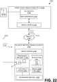
- an exemplary apparatus comprises a network interface adapted to receive a valid key code and a guided surface wave receive structure configured to obtain electrical energy from a guided surface wave traveling along a terrestrial medium, in which the guided surface wave is embedded with a user key code.
- the apparatus further comprises processing circuitry adapted to validate the user key code against the valid key code and an electrical load coupled to the guided surface wave receive structure, wherein the processing circuitry is adapted to disable delivery of the electrical energy from the guided surface wave to the electrical load responsive to the user key code being invalidated.
- the electrical is experienced as a load at an excitation source coupled to a guided surface waveguide probe generating the guided surface wave.
- another exemplary apparatus comprises a guided surface waveguide probe configured to launch a guided surface wave over a lossy conducting medium and modulation circuitry configured to embed a valid key code within the guided surface wave.
- Such an apparatus further comprises a controller device further configured to transmit a user key code in an out-of-band communication channel to guided surface wave receive equipment that is configured to receive the guided surface wave, wherein a positive comparison of the user key code against the valid key code indicates an authorization to deliver electrical energy obtained from the guided surface wave to an electrical load.
- an exemplary method comprises obtaining, via processing circuitry coupled to guided surface wave receive structure, a user key code; receiving electrical energy in a form of a guided surface wave using the guided surface wave receive structure, wherein the electrical energy is embedded with a valid key code; processing, via the processing circuitry, the guided surface wave to obtain the user key code; validating, via the processing circuitry, the user key code to compare against the valid key code, wherein the processing circuitry is adapted to disable delivery of the electrical energy from the guided surface wave to an electrical load responsive to the user key code being invalidated; and supplying the electrical energy to an electrical load coupled to the guided surface wave receive structure responsive to a validated user key code.
- a radiated electromagnetic field comprises electromagnetic energy that is emitted from a source structure in the form of waves that are not bound to a waveguide.
- a radiated electromagnetic field is generally a field that leaves an electric structure such as an antenna and propagates through the atmosphere or other medium and is not bound to any waveguide structure. Once radiated electromagnetic waves leave an electric structure such as an antenna, they continue to propagate in the medium of propagation (such as air) independent of their source until they dissipate regardless of whether the source continues to operate. Once electromagnetic waves are radiated, they are not recoverable unless intercepted, and, if not intercepted, the energy inherent in the radiated electromagnetic waves is lost forever.
- Radio structures such as antennas are designed to radiate electromagnetic fields by maximizing the ratio of the radiation resistance to the structure loss resistance. Radiated energy spreads out in space and is lost regardless of whether a receiver is present. The energy density of the radiated fields is a function of distance due to geometric spreading. Accordingly, the term "radiate" in all its forms as used herein refers to this form of electromagnetic propagation.
- a guided electromagnetic field is a propagating electromagnetic wave whose energy is concentrated within or near boundaries between media having different electromagnetic properties.
- a guided electromagnetic field is one that is bound to a waveguide and may be characterized as being conveyed by the current flowing in the waveguide. If there is no load to receive and/or dissipate the energy conveyed in a guided electromagnetic wave, then no energy is lost except for that dissipated in the conductivity of the guiding medium. Stated another way, if there is no load for a guided electromagnetic wave, then no energy is consumed.
- a generator or other source generating a guided electromagnetic field does not deliver real power unless a resistive load is present. To this end, such a generator or other source essentially runs idle until a load is presented.
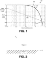
- FIG. 1 shown is a graph 100 of field strength in decibels (dB) above an arbitrary reference in volts per meter as a function of distance in kilometers on a log-dB plot to further illustrate the distinction between radiated and guided electromagnetic fields.
- the graph 100 of FIG. 1 depicts a guided field strength curve 103 that shows the field strength of a guided electromagnetic field as a function of distance.
- This guided field strength curve 103 is essentially the same as a transmission line mode.
- the graph 100 of FIG. 1 depicts a radiated field strength curve 106 that shows the field strength of a radiated electromagnetic field as a function of distance.
- the radiated field strength curve 106 falls off geometrically (1/ d , where d is distance), which is depicted as a straight line on the log-log scale.
- the guided field strength curve 103 has a characteristic exponential decay of e ⁇ ⁇ d / d and exhibits a distinctive knee 109 on the log-log scale.
- the guided field strength curve 103 and the radiated field strength curve 106 intersect at point 112, which occurs at a crossing distance. At distances less than the crossing distance at intersection point 112, the field strength of a guided electromagnetic field is significantly greater at most locations than the field strength of a radiated electromagnetic field.
- the guided and radiated field strength curves 103 and 106 further illustrate the fundamental propagation difference between guided and radiated electromagnetic fields.
- Milligan T., Modern Antenna Design, McGraw-Hill, 1st Edition, 1985, pp.8-9 .
- the wave equation is a differential operator whose eigenfunctions possess a continuous spectrum of eigenvalues on the complex wave-number plane.
- This transverse electro-magnetic (TEM) field is called the radiation field, and those propagating fields are called "Hertzian waves.”
- TEM transverse electro-magnetic
- the wave equation plus boundary conditions mathematically lead to a spectral representation of wave-numbers composed of a continuous spectrum plus a sum of discrete spectra.
- Sommerfeld, A. "Uber die Ausbreitung der Wellen in der Drahtlosen Telegraphie," Annalen der Physik, Vol. 28, 1909, pp. 665-736 .
- ground wave and "surface wave” identify two distinctly different physical propagation phenomena.
- a surface wave arises analytically from a distinct pole yielding a discrete component in the plane wave spectrum. See, e.g., " The Excitation of Plane Surface Waves” by Cullen, A.L., (Proceedings of the IEE (British), Vol. 101, Part IV, August 1954, pp. 225-235 ).
- a surface wave is considered to be a guided surface wave.
- the surface wave in the Zenneck-Sommerfeld guided wave sense
- no t the same as the ground wave (in the Weyl-Norton-FCC sense) that is now so familiar from radio broadcasting.
- the continuous part of the wave-number eigenvalue spectrum produces the radiation field
- the discrete spectra, and corresponding residue sum arising from the poles enclosed by the contour of integration result in non-TEM traveling surface waves that are exponentially damped in the direction transverse to the propagation.
- Such surface waves are guided transmission line modes.
- Friedman, B. Principles and Techniques of Applied Mathematics, Wiley, 1956, pp. pp. 214, 283-286, 290, 298-300 .
- antennas In free space, antennas excite the continuum eigenvalues of the wave equation, which is a radiation field, where the outwardly propagating RF energy with E z and H ⁇ in-phase is lost forever.
- waveguide probes excite discrete eigenvalues, which results in transmission line propagation. See Collin, R. E., Field Theory of Guided Waves, McGraw-Hill, 1960, pp. 453, 474-477 . While such theoretical analyses have held out the hypothetical possibility of launching open surface guided waves over planar or spherical surfaces of lossy, homogeneous media, for more than a century no known structures in the engineering arts have existed for accomplishing this with any practical efficiency.
- various guided surface waveguide probes are described that are configured to excite electric fields that couple into a guided surface waveguide mode along the surface of a lossy conducting medium.
- Such guided electromagnetic fields are substantially mode-matched in magnitude and phase to a guided surface wave mode on the surface of the lossy conducting medium.
- Such a guided surface wave mode can also be termed a Zenneck waveguide mode.
- the resultant fields excited by the guided surface waveguide probes described herein are substantially mode-matched to a guided surface waveguide mode on the surface of the lossy conducting medium, a guided electromagnetic field in the form of a guided surface wave is launched along the surface of the lossy conducting medium.
- the lossy conducting medium comprises a terrestrial medium such as the Earth.
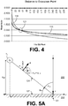
- FIG. 2 shown is a propagation interface that provides for an examination of the boundary value solutions to Maxwell's equations derived in 1907 by Jonathan Zenneck as set forth in his paper Zenneck, J., "On the Propagation of Plane Electromagnetic Waves Along a Flat Conducting Surface and their Relation to Wireless Telegraphy," Annalen der Physik, Serial 4, Vol. 23, September 20, 1907, pp. 846-866 .
- FIG. 2 depicts cylindrical coordinates for radially propagating waves along the interface between a lossy conducting medium specified as Region 1 and an insulator specified as Region 2.
- Region 1 can comprise, for example, any lossy conducting medium.
- such a lossy conducting medium can comprise a terrestrial medium such as the Earth or other medium.
- Region 2 is a second medium that shares a boundary interface with Region 1 and has different constitutive parameters relative to Region 1.
- Region 2 can comprise, for example, any insulator such as the atmosphere or other medium.
- the reflection coefficient for such a boundary interface goes to zero only for incidence at a complex Brewster angle. See Stratton, J.A., Electromagnetic Theory, McGraw-Hill, 1941, p. 516 .
- the present disclosure sets forth various guided surface waveguide probes that generate electromagnetic fields that are substantially mode-matched to a guided surface waveguide mode on the surface of the lossy conducting medium comprising Region 1.
- such electromagnetic fields substantially synthesize a wave front incident at a complex Brewster angle of the lossy conducting medium that can result in zero reflection.
- z is the vertical coordinate normal to the surface of Region 1 and ⁇ is the radial coordinate
- H n 2 ⁇ j ⁇ is a complex argument Hankel function of the second kind and order n
- u 1 is the propagation constant in the positive vertical ( z ) direction in Region 1
- u 2 is the propagation constant in the vertical ( z ) direction in Region 2
- ⁇ 1 is the conductivity of Region 1
- ⁇ is equal to 2 ⁇ f, where f is a frequency of excitation
- ⁇ o is the permittivity of free space
- ⁇ 1 is the permittivity of Region 1
- A is a source constant imposed by the source
- ⁇ is a surface wave radial propagation constant.
- x ⁇ 1 ⁇ o
- ⁇ r comprises the relative permittivity of Region 1
- ⁇ 1 is the conductivity of Region 1
- ⁇ o is the permittivity of free space
- ⁇ o comprises the permeability of free space.
- Equations (1)-(3) can be considered to be a cylindrically-symmetric, radially-propagating waveguide mode. See Barlow, H. M., and Brown, J., Radio Surface Waves, Oxford University Press, 1962, pp. 10-12, 29-33 .
- the present disclosure details structures that excite this "open boundary" waveguide mode.
- a guided surface waveguide probe is provided with a charge terminal of appropriate size that is fed with voltage and/or current and is positioned relative to the boundary interface between Region 2 and Region 1. This may be better understood with reference to FIG.
- FIG 3 which shows an example of a guided surface waveguide probe 200a that includes a charge terminal T 1 elevated above a lossy conducting medium 203 (e.g., the Earth) along a vertical axis z that is normal to a plane presented by the lossy conducting medium 203.
- the lossy conducting medium 203 makes up Region 1
- a second medium 206 makes up Region 2 and shares a boundary interface with the lossy conducting medium 203.
- the lossy conducting medium 203 can comprise a terrestrial medium such as the planet Earth.
- a terrestrial medium comprises all structures or formations included thereon whether natural or man-made.
- such a terrestrial medium can comprise natural elements such as rock, soil, sand, fresh water, sea water, trees, vegetation, and all other natural elements that make up our planet.
- such a terrestrial medium can comprise man-made elements such as concrete, asphalt, building materials, and other man-made materials.
- the lossy conducting medium 203 can comprise some medium other than the Earth, whether naturally occurring or man-made.
- the lossy conducting medium 203 can comprise other media such as man-made surfaces and structures such as automobiles, aircraft, man-made materials (such as plywood, plastic sheeting, or other materials) or other media.
- the second medium 206 can comprise the atmosphere above the ground.
- the atmosphere can be termed an "atmospheric medium” that comprises air and other elements that make up the atmosphere of the Earth.
- the second medium 206 can comprise other media relative to the lossy conducting medium 203.
- the guided surface waveguide probe 200a includes a feed network 209 that couples an excitation source 212 to the charge terminal T 1 via, e.g., a vertical feed line conductor.
- a charge Q 1 is imposed on the charge terminal T 1 to synthesize an electric field based upon the voltage applied to terminal T 1 at any given instant.
- ⁇ i the angle of incidence
- E the electric field
- Equations (1)-(6) and (17) have the nature of a transmission line mode bound to a lossy interface, not radiation fields that are associated with groundwave propagation. See Barlow, H. M. and Brown, J., Radio Surface Waves, Oxford University Press, 1962, pp. 1-5 .
- Equations (1)-(6) and (17) a review of the nature of the Hankel functions used in Equations (1)-(6) and (17) is provided for these solutions of the wave equation.
- H n 2 k ⁇ ⁇ is an outgoing wave can be recognized from its large argument asymptotic behavior that is obtained directly from the series definitions of J n (x) and N n (x).
- H n 2 x ⁇ x ⁇ ⁇ 2 ⁇ j ⁇ x j n e ⁇ jx 2 ⁇ x j n e ⁇ j x ⁇ ⁇ 4 , which, when multiplied by e j ⁇ t , is an outward propagating cylindrical wave of the form e j ( ⁇ t-k ⁇ ) with a 1 / ⁇ spatial variation.
- the Hankel function of first order and the second kind behaves as H 1 2 x ⁇ x ⁇ 0 2 ⁇ j ⁇ x . Note that these asymptotic expressions are complex quantities.
- Equations (20b) and (21) differ in phase by j , which corresponds to an extra phase advance or "phase boost" of 45° or, equivalently, ⁇ /8.
- the "far out” representation predominates over the "close-in” representation of the Hankel function.
- the distance to the Hankel crossover point (or Hankel crossover distance) can be found by equating Equations (20b) and (21) for -jyp, and solving for R x .
- x ⁇ / ⁇ 0
- the far-out and close-in Hankel function asymptotes are frequency dependent, with the Hankel crossover point moving out as the frequency is lowered.
- the Hankel function asymptotes may also vary as the conductivity ( ⁇ ) of the lossy conducting medium changes. For example, the conductivity of the soil can vary with changes in weather conditions.
- the height H 1 of the elevated charge terminal T 1 in FIG. 3 affects the amount of free charge on the charge terminal T 1 .
- the charge terminal T 1 is near the ground plane of Region 1, most of the charge Q 1 on the terminal is "bound."
- the bound charge is lessened until the charge terminal T 1 reaches a height at which substantially all of the isolated charge is free.
- the advantage of an increased capacitive elevation for the charge terminal T 1 is that the charge on the elevated charge terminal T 1 is further removed from the ground plane, resulting in an increased amount of free charge q free to couple energy into the guided surface waveguide mode. As the charge terminal T 1 is moved away from the ground plane, the charge distribution becomes more uniformly distributed about the surface of the terminal. The amount of free charge is related to the self-capacitance of the charge terminal T 1 .
- the capacitance of a spherical terminal can be expressed as a function of physical height above the ground plane.
- an increase in the terminal height h reduces the capacitance C of the charge terminal.
- the charge distribution is approximately uniform about the spherical terminal, which can improve the coupling into the guided surface waveguide mode.
- the charge terminal T 1 can include any shape such as a sphere, a disk, a cylinder, a cone, a torus, a hood, one or more rings, or any other randomized shape or combination of shapes.
- An equivalent spherical diameter can be determined and used for positioning of the charge terminal T 1 .
- the charge terminal T 1 can be positioned at a physical height that is at least four times the spherical diameter (or equivalent spherical diameter) of the charge terminal T 1 to reduce the bounded charge effects.
- FIG. 5A shown is a ray optics interpretation of the electric field produced by the elevated charge Q 1 on charge terminal T 1 of FIG. 3 .
- minimizing the reflection of the incident electric field can improve and/or maximize the energy coupled into the guided surface waveguide mode of the lossy conducting medium 203.
- the ray optic interpretation shows the incident field polarized parallel to the plane of incidence having an angle of incidence of ⁇ i , which is measured with respect to the surface normal ( ⁇ ).
- This complex angle of incidence ( ⁇ i,B ) is referred to as the Brewster angle.
- Equation (22) it can be seen that the same complex Brewster angle ( ⁇ i,B ) relationship is present in both Equations (22) and (26).
- the electric field vector E can be depicted as an incoming non-uniform plane wave, polarized parallel to the plane of incidence.
- E ⁇ ⁇ i E ⁇ ⁇ ⁇ + E z z ⁇ .
- E ⁇ ⁇ z E ⁇ z cos ⁇ i
- the wave tilt angle ( ⁇ ) is equal to the angle between the normal of the wave-front at the boundary interface with Region 1 and the tangent to the boundary interface. This may be easier to see in FIG. 5B , which illustrates equi-phase surfaces of an electromagnetic wave and their normals for a radial cylindrical guided surface wave.
- the concept of an electrical effective height can provide further insight into synthesizing an electric field with a complex angle of incidence with a guided surface waveguide probe 200.
- the integration of the distributed current I ( z ) of the structure is performed over the physical height of the structure ( h p ), and normalized to the ground current ( I 0 ) flowing upward through the base (or input) of the structure.
- I C is the current that is distributed along the vertical structure of the guided surface waveguide probe 200a.
- the phase delay is measured relative to the ground (stake) current I 0 .
- ray optics are used to illustrate the complex angle trigonometry of the incident electric field ( E ) having a complex Brewster angle of incidence ( ⁇ i,B ) at the Hankel crossover distance ( R x ) 121.
- a right triangle is depicted having an adjacent side of length R x along the lossy conducting medium surface and a complex Brewster angle ⁇ i,B measured between a ray 124 extending between the Hankel crossover point 121 at R x and the center of the charge terminal T 1 , and the lossy conducting medium surface 127 between the Hankel crossover point 121 and the charge terminal T 1 .
- the charge terminal T 1 positioned at physical height h p and excited with a charge having the appropriate phase delay ⁇ , the resulting electric field is incident with the lossy conducting medium boundary interface at the Hankel crossover distance R x , and at the Brewster angle. Under these conditions, the guided surface waveguide mode can be excited without reflection or substantially negligible reflection.
- FIG. 6 graphically illustrates the effect of decreasing the physical height of the charge terminal T 1 on the distance where the electric field is incident at the Brewster angle.
- the point where the electric field intersects with the lossy conducting medium (e.g., the Earth) at the Brewster angle moves closer to the charge terminal position.
- Equation (39) indicates, the height H 1 ( FIG.
- the height of the charge terminal T 1 should be at or higher than the physical height ( h p ) in order to excite the far-out component of the Hankel function.
- the height should be at least four times the spherical diameter (or equivalent spherical diameter) of the charge terminal T 1 as mentioned above.
- a guided surface waveguide probe 200 can be configured to establish an electric field having a wave tilt that corresponds to a wave illuminating the surface of the lossy conducting medium 203 at a complex Brewster angle, thereby exciting radial surface currents by substantially mode-matching to a guided surface wave mode at (or beyond) the Hankel crossover point 121 at R x .
- FIG. 7 shown is a graphical representation of an example of a guided surface waveguide probe 200b that includes a charge terminal T 1 .
- An AC source 212 acts as the excitation source for the charge terminal T 1 , which is coupled to the guided surface waveguide probe 200b through a feed network 209 ( FIG. 3 ) comprising a coil 215 such as, e.g., a helical coil.
- the AC source 212 can be inductively coupled to the coil 215 through a primary coil.
- an impedance matching network may be included to improve and/or maximize coupling of the AC source 212 to the coil 215.
- the guided surface waveguide probe 200b can include the upper charge terminal T 1 (e.g., a sphere at height h p ) that is positioned along a vertical axis z that is substantially normal to the plane presented by the lossy conducting medium 203.
- a second medium 206 is located above the lossy conducting medium 203.
- the charge terminal T 1 has a self-capacitance C T .
- charge Q 1 is imposed on the terminal T 1 depending on the voltage applied to the terminal T 1 at any given instant.
- the coil 215 is coupled to a ground stake 218 at a first end and to the charge terminal T 1 via a vertical feed line conductor 221.
- the coil connection to the charge terminal T 1 can be adjusted using a tap 224 of the coil 215 as shown in FIG. 7 .
- the coil 215 can be energized at an operating frequency by the AC source 212 through a tap 227 at a lower portion of the coil 215.
- the AC source 212 can be inductively coupled to the coil 215 through a primary coil.
- the construction and adjustment of the guided surface waveguide probe 200 is based upon various operating conditions, such as the transmission frequency, conditions of the lossy conducting medium (e.g., soil conductivity ⁇ and relative permittivity ⁇ r ), and size of the charge terminal T 1 .
- the conductivity ⁇ and relative permittivity ⁇ r can be determined through test measurements of the lossy conducting medium 203.
- the wave tilt at the Hankel crossover distance (W Rx ) can also be found using Equation (40).
- the Hankel crossover distance can also be found by equating the magnitudes of Equations (20b) and (21) for -jyp, and solving for R x as illustrated by FIG. 4 .
- the complex effective height ( h eff ) includes a magnitude that is associated with the physical height ( h p ) of the charge terminal T 1 and a phase delay ( ⁇ ) that is to be associated with the angle ( ⁇ ) of the wave tilt at the Hankel crossover distance ( R x ).
- the feed network 209 ( FIG. 3 ) and/or the vertical feed line connecting the feed network to the charge terminal T 1 can be adjusted to match the phase ( ⁇ ) of the charge Q 1 on the charge terminal T 1 to the angle ( ⁇ ) of the wave tilt ( W ).
- the size of the charge terminal T 1 can be chosen to provide a sufficiently large surface for the charge Q 1 imposed on the terminals. In general, it is desirable to make the charge terminal T 1 as large as practical. The size of the charge terminal T 1 should be large enough to avoid ionization of the surrounding air, which can result in electrical discharge or sparking around the charge terminal.
- phase delay ⁇ c of a helically-wound coil can be determined from Maxwell's equations as has been discussed by Corum, K.L. and J.F. Corum, "RF Coils, Helical Resonators and Voltage Magnification by Coherent Spatial Modes," Microwave Review, Vol. 7, No. 2, September 2001, pp. 36-45 ., which is incorporated herein by reference in its entirety.
- H the axial length of the solenoidal helix
- D the coil diameter
- N the number of turns of the coil
- ⁇ 0 the free-space wavelength
- the principle is the same if the helix is wound spirally or is short and fat, but V f and ⁇ c are easier to obtain by experimental measurement.
- the spatial phase delay ⁇ y of the structure can be determined using the traveling wave phase delay of the vertical feed line conductor 221 ( FIG. 7 ).
- the velocity factor is a constant with V w ⁇ 0.94, or in a range from about 0.93 to about 0.98.
- Z w 138 log 1.123 V w ⁇ 0 2 ⁇ ⁇ a . Equation (51) implies that Z w for a single-wire feeder varies with frequency. The phase delay can be determined based upon the capacitance and characteristic impedance.
- the electric field produced by the charge oscillating Q 1 on the charge terminal T 1 is coupled into a guided surface waveguide mode traveling along the surface of a lossy conducting medium 203. For example, if the Brewster angle ( ⁇ i , B ), the phase delay ( ⁇ y ) associated with the vertical feed line conductor 221 ( FIG. 7 ), and the configuration of the coil 215 ( FIG.
- the position of the tap 224 may be adjusted to maximize coupling the traveling surface waves into the guided surface waveguide mode. Excess coil length beyond the position of the tap 224 can be removed to reduce the capacitive effects.
- the vertical wire height and/or the geometrical parameters of the helical coil may also be varied.
- the coupling to the guided surface waveguide mode on the surface of the lossy conducting medium 203 can be improved and/or optimized by tuning the guided surface waveguide probe 200 for standing wave resonance with respect to a complex image plane associated with the charge Q 1 on the charge terminal T 1 .
- the performance of the guided surface waveguide probe 200 can be adjusted for increased and/or maximum voltage (and thus charge Q 1 ) on the charge terminal T 1 .
- the effect of the lossy conducting medium 203 in Region 1 can be examined using image theory analysis.
- an elevated charge Q 1 placed over a perfectly conducting plane attracts the free charge on the perfectly conducting plane, which then "piles up” in the region under the elevated charge Q 1 .
- the resulting distribution of "bound” electricity on the perfectly conducting plane is similar to a bell-shaped curve.
- the boundary value problem solution that describes the fields in the region above the perfectly conducting plane may be obtained using the classical notion of image charges, where the field from the elevated charge is superimposed with the field from a corresponding "image" charge below the perfectly conducting plane.
- This analysis may also be used with respect to a lossy conducting medium 203 by assuming the presence of an effective image charge Q 1 ' beneath the guided surface waveguide probe 200.
- the effective image charge Q 1 ' coincides with the charge Q 1 on the charge terminal T 1 about a conducting image ground plane 130, as illustrated in FIG. 3 .
- the image charge Q 1 ' is not merely located at some real depth and 180° out of phase with the primary source charge Q 1 on the charge terminal T 1 , as they would be in the case of a perfect conductor. Rather, the lossy conducting medium 203 (e.g., a terrestrial medium) presents a phase shifted image.
- the image charge Q 1 ' is at a complex depth below the surface (or physical boundary) of the lossy conducting medium 203.
- complex image depth reference is made to Wait, J. R., "Complex Image Theory-Revisited,” IEEE Antennas and Propagation Magazine, Vol. 33, No. 4, August 1991, pp. 27-29 .
- the complex spacing of the image charge implies that the external field will experience extra phase shifts not encountered when the interface is either a dielectric or a perfect conductor.
- the lossy conducting medium 203 is a finitely conducting Earth 133 with a physical boundary 136.
- the finitely conducting Earth 133 may be replaced by a perfectly conducting image ground plane 139 as shown in FIG.8B , which is located at a complex depth z 1 below the physical boundary 136.
- This equivalent representation exhibits the same impedance when looking down into the interface at the physical boundary 136.
- the equivalent representation of FIG. 8B can be modeled as an equivalent transmission line, as shown in FIG. 8C .
- the depth z 1 can be determined by equating the TEM wave impedance looking down at the Earth to an image ground plane impedance z in seen looking into the transmission line of FIG. 8C .
- the guided surface waveguide probe 200b of FIG. 7 can be modeled as an equivalent single-wire transmission line image plane model that can be based upon the perfectly conducting image ground plane 139 of FIG. 8B .
- FIG. 9A shows an example of the equivalent single-wire transmission line image plane model
- FIG. 9B illustrates an example of the equivalent classic transmission line model, including the shorted transmission line of FIG. 8C .
- Z w is the characteristic impedance of the elevated vertical feed line conductor 221 in ohms
- Z c is the characteristic impedance of the coil 215 in ohms
- Z o is the characteristic impedance of free space.
- Z L 1 j ⁇ C T
- C T is the self-capacitance of the charge terminal T 1
- the impedance seen "looking up” into the vertical feed line conductor 221 FIG.
- Z base Z c Z 2 + Z c tanh j ⁇ p H
- Z c + Z 2 tanh j ⁇ p H Z c Z 2 + Z c tanh j ⁇ c Z c + Z 2 tanh j ⁇ c .
- the impedance at the physical boundary 136 "looking up" into the guided surface waveguide probe 200 is the conjugate of the impedance at the physical boundary 136 "looking down" into the lossy conducting medium 203.
- the equivalent image plane models of FIGS. 9A and 9B can be tuned to resonance with respect to the image ground plane 139.
- the impedance of the equivalent complex image plane model is purely resistive, which maintains a superposed standing wave on the probe structure that maximizes the voltage and elevated charge on terminal T 1 , and by equations (1)-(3) and (16) maximizes the propagating surface wave.
- the guided surface wave excited by the guided surface waveguide probe 200 is an outward propagating traveling wave .
- the source distribution along the feed network 209 between the charge terminal T 1 and the ground stake 218 of the guided surface waveguide probe 200 ( FIGS. 3 and 7 ) is actually composed of a superposition of a traveling wave plus a standing wave on the structure.
- the phase delay of the traveling wave moving through the feed network 209 is matched to the angle of the wave tilt associated with the lossy conducting medium 203. This mode-matching allows the traveling wave to be launched along the lossy conducting medium 203.
- the load impedance Z L of the charge terminal T 1 is adjusted to bring the probe structure into standing wave resonance with respect to the image ground plane (130 of FIG. 3 or 139 of FIG. 8 ), which is at a complex depth of - d/2. In that case, the impedance seen from the image ground plane has zero reactance and the charge on the charge terminal T 1 is maximized.
- two relatively short transmission line sections of widely differing characteristic impedance may be used to provide a very large phase shift.
- a probe structure composed of two sections of transmission line, one of low impedance and one of high impedance, together totaling a physical length of, say, 0.05 ⁇ , may be fabricated to provide a phase shift of 90° which is equivalent to a 0.25 ⁇ resonance. This is due to the large jump in characteristic impedances.
- a physically short probe structure can be electrically longer than the two physical lengths combined. This is illustrated in FIGS. 9A and 9B , where the discontinuities in the impedance ratios provide large jumps in phase. The impedance discontinuity provides a substantial phase shift where the sections are joined together.
- FIG. 10 shown is a flow chart 150 illustrating an example of adjusting a guided surface waveguide probe 200 ( FIGS. 3 and 7 ) to substantially mode-match to a guided surface waveguide mode on the surface of the lossy conducting medium, which launches a guided surface traveling wave along the surface of a lossy conducting medium 203 ( FIG. 3 ).
- the charge terminal T 1 of the guided surface waveguide probe 200 is positioned at a defined height above a lossy conducting medium 203.
- the Hankel crossover distance can also be found by equating the magnitudes of Equations (20b) and (21) for -jyp, and solving for R x as illustrated by FIG. 4 .
- the complex index of refraction (n) can be determined using Equation (41), and the complex Brewster angle ( ⁇ i,B ) can then be determined from Equation (42).
- the physical height ( h p ) of the charge terminal T 1 can then be determined from Equation (44).
- the charge terminal T 1 should be at or higher than the physical height ( h p ) in order to excite the far-out component of the Hankel function. This height relationship is initially considered when launching surface waves.
- the height should be at least four times the spherical diameter (or equivalent spherical diameter) of the charge terminal T 1 .
- the electrical phase delay ⁇ of the elevated charge Q 1 on the charge terminal T 1 is matched to the complex wave tilt angle ⁇ .
- the phase delay ( ⁇ c ) of the helical coil and/or the phase delay ( ⁇ y ) of the vertical feed line conductor can be adjusted to make ⁇ equal to the angle ( ⁇ ) of the wave tilt ( W ).
- the electrical phase ⁇ can then be matched to the angle of the wave tilt. This angular (or phase) relationship is next considered when launching surface waves.
- ⁇ ⁇
- an electric field can be established at or beyond the Hankel crossover distance ( R x ) with a complex Brewster angle at the boundary interface to excite the surface waveguide mode and launch a traveling wave along the lossy conducting medium 203.
- the load impedance of the charge terminal T 1 is tuned to resonate the equivalent image plane model of the guided surface waveguide probe 200.
- the depth (d/2) of the conducting image ground plane 139 of FIG. 9A and 9B (or 130 of FIG. 3 ) can be determined using Equations (52), (53) and (54) and the values of the lossy conducting medium 203 (e.g., the Earth), which can be measured.
- the impedance ( Z in ) as seen "looking down" into the lossy conducting medium 203 can then be determined using Equation (65). This resonance relationship can be considered to maximize the launched surface waves.
- the velocity factor, phase delay, and impedance of the coil 215 and vertical feed line conductor 221 can be determined using Equations (45) through (51).
- the self-capacitance ( C T ) of the charge terminal T 1 can be determined using, e.g., Equation (24).
- the propagation factor ( ⁇ p ) of the coil 215 can be determined using Equation (35) and the propagation phase constant ( ⁇ w ) for the vertical feed line conductor 221 can be determined using Equation (49).
- the impedance ( Z base ) of the guided surface waveguide probe 200 as seen "looking up” into the coil 215 can be determined using Equations (62), (63) and (64).
- the impedance at the physical boundary 136 "looking up" into the guided surface waveguide probe 200 is the conjugate of the impedance at the physical boundary 136 "looking down" into the lossy conducting medium 203.
- An iterative approach may be taken to tune the load impedance Z L for resonance of the equivalent image plane model with respect to the conducting image ground plane 139 (or 130). In this way, the coupling of the electric field to a guided surface waveguide mode along the surface of the lossy conducting medium 203 (e.g., Earth) can be improved and/or maximized.
- the lossy conducting medium 203 e.g., Earth
- ⁇ will equal ⁇ to match the guided surface waveguide mode.
- FIG. 11 shows a plot of both over a range of frequencies. As both ⁇ and ⁇ are frequency dependent, it can be seen that their respective curves cross over each other at approximately 1.85 MHz.
- the load impedance ( Z L ) of the charge terminal T 1 can be adjusted for standing wave resonance of the equivalent image plane model of the guided surface wave probe 200.
- the coupling into the guided surface waveguide mode may be maximized.
- This can be accomplished by adjusting the capacitance of the charge terminal T 1 without changing the traveling wave phase delays of the coil and vertical feed line conductor.
- the guided field strength curve 103 of the guided electromagnetic field has a characteristic exponential decay of e ⁇ ⁇ d / d and exhibits a distinctive knee 109 on the log-log scale.
- the surface waveguide may be considered to be "mode-matched".
- the charge terminal T 1 is of sufficient height H 1 of FIG. 3 ( h ⁇ R x tan ⁇ i,B ) so that electromagnetic waves incident onto the lossy conducting medium 203 at the complex Brewster angle do so out at a distance ( ⁇ R x ) where the 1 / r term is predominant.
- Receive circuits can be utilized with one or more guided surface waveguide probes to facilitate wireless transmission and/or power delivery systems.
- operation of a guided surface waveguide probe 200 may be controlled to adjust for variations in operational conditions associated with the guided surface waveguide probe 200.
- an adaptive probe control system 230 can be used to control the feed network 209 and/or the charge terminal T 1 to control the operation of the guided surface waveguide probe 200.
- Operational conditions can include, but are not limited to, variations in the characteristics of the lossy conducting medium 203 (e.g. , conductivity ⁇ and relative permittivity ⁇ r ), variations in field strength and/or variations in loading of the guided surface waveguide probe 200.
- e j ⁇ ) can be affected by changes in soil conductivity and permittivity resulting from, e.g., weather conditions.
- Equipment such as, e.g., conductivity measurement probes, permittivity sensors, ground parameter meters, field meters, current monitors and/or load receivers can be used to monitor for changes in the operational conditions and provide information about current operational conditions to the adaptive probe control system 230.
- the probe control system 230 can then make one or more adjustments to the guided surface waveguide probe 200 to maintain specified operational conditions for the guided surface waveguide probe 200. For instance, as the moisture and temperature vary, the conductivity of the soil will also vary.
- Conductivity measurement probes and/or permittivity sensors may be located at multiple locations around the guided surface waveguide probe 200. Generally, it would be desirable to monitor the conductivity and/or permittivity at or about the Hankel crossover distance R x for the operational frequency.
- Conductivity measurement probes and/or permittivity sensors may be located at multiple locations ( e.g., in each quadrant) around the guided surface waveguide probe 200.
- the conductivity measurement probes and/or permittivity sensors can be configured to evaluate the conductivity and/or permittivity on a periodic basis and communicate the information to the probe control system 230.
- the information may be communicated to the probe control system 230 through a network such as, but not limited to, a LAN, WLAN, cellular network, or other appropriate wired or wireless communication network.
- the probe control system 230 may evaluate the variation in the index of refraction ( n ), the complex Brewster angle ( ⁇ i , B ), and/or the wave tilt (
- the probe control system 230 can adjust the self-capacitance of the charge terminal T 1 and/or the phase delay ( ⁇ y , ⁇ c ) applied to the charge terminal T 1 to maintain the electrical launching efficiency of the guided surface wave at or near its maximum.
- the self-capacitance of the charge terminal T 1 can be varied by changing the size of the terminal.
- the charge distribution can also be improved by increasing the size of the charge terminal T 1 , which can reduce the chance of an electrical discharge from the charge terminal T 1 .
- the charge terminal T 1 can include a variable inductance that can be adjusted to change the load impedance Z L .
- the phase applied to the charge terminal T 1 can be adjusted by varying the tap position on the coil 215 ( FIG. 7 ), and/or by including a plurality of predefined taps along the coil 215 and switching between the different predefined tap locations to maximize the launching efficiency.
- Field or field strength (FS) meters may also be distributed about the guided surface waveguide probe 200 to measure field strength of fields associated with the guided surface wave.
- the field or FS meters can be configured to detect the field strength and/or changes in the field strength (e.g., electric field strength) and communicate that information to the probe control system 230.
- the information may be communicated to the probe control system 230 through a network such as, but not limited to, a LAN, WLAN, cellular network, or other appropriate communication network.
- the guided surface waveguide probe 200 may be adjusted to maintain specified field strength(s) at the FS meter locations to ensure appropriate power transmission to the receivers and the loads they supply.
- the guided surface waveguide probe 200 can be adjusted to ensure the wave tilt corresponds to the complex Brewster angle. This can be accomplished by adjusting a tap position on the coil 215 ( FIG. 7 ) to change the phase delay supplied to the charge terminal T 1 .
- the voltage level supplied to the charge terminal T 1 can also be increased or decreased to adjust the electric field strength. This may be accomplished by adjusting the output voltage of the excitation source 212 or by adjusting or reconfiguring the feed network 209. For instance, the position of the tap 227 ( FIG.
- the AC source 212 can be adjusted to increase the voltage seen by the charge terminal T 1 . Maintaining field strength levels within predefined ranges can improve coupling by the receivers, reduce ground current losses, and avoid interference with transmissions from other guided surface waveguide probes 200.
- the probe control system 230 can be implemented with hardware, firmware, software executed by hardware, or a combination thereof.
- the probe control system 230 can include processing circuitry including a processor and a memory, both of which can be coupled to a local interface such as, for example, a data bus with an accompanying control/address bus as can be appreciated by those with ordinary skill in the art.
- a probe control application may be executed by the processor to adjust the operation of the guided surface waveguide probe 200 based upon monitored conditions.
- the probe control system 230 can also include one or more network interfaces for communicating with the various monitoring devices. Communications can be through a network such as, but not limited to, a LAN, WLAN, cellular network, or other appropriate communication network.
- the probe control system 230 may comprise, for example, a computer system such as a server, desktop computer, laptop, or other system with like capability.
- the complex angle trigonometry is shown for the ray optic interpretation of the incident electric field ( E ) of the charge terminal T 1 with a complex Brewster angle ( ⁇ i,B ) at the Hankel crossover distance ( R x ).
- the Brewster angle is complex and specified by equation (38).
- the geometric parameters are related by the electrical effective height ( h eff ) of the charge terminal T 1 by equation (39).
- the angle of the desired guided surface wave tilt at the Hankel crossover distance (W Rx ) is equal to the phase ( ⁇ ) of the complex effective height ( h eff ) .
- Equation (39) means that the physical height of the guided surface waveguide probe 200 can be relatively small. While this will excite the guided surface waveguide mode, this can result in an unduly large bound charge with little free charge.
- the charge terminal T 1 can be raised to an appropriate elevation to increase the amount of free charge. As one example rule of thumb, the charge terminal T 1 can be positioned at an elevation of about 4-5 times (or more) the effective diameter of the charge terminal T 1 .
- FIG. 6 illustrates the effect of raising the charge terminal T 1 above the physical height ( h p ) shown in FIG. 5A . The increased elevation causes the distance at which the wave tilt is incident with the lossy conductive medium to move beyond the Hankel crossover point 121 ( FIG. 5A ).
- a lower compensation terminal T 2 can be used to adjust the total effective height ( h TE ) of the charge terminal T 1 such that the wave tilt at the Hankel crossover distance is at the Brewster angle.
- a guided surface waveguide probe 200c that includes an elevated charge terminal T 1 and a lower compensation terminal T 2 that are arranged along a vertical axis z that is normal to a plane presented by the lossy conducting medium 203.
- the charge terminal T 1 is placed directly above the compensation terminal T 2 although it is possible that some other arrangement of two or more charge and/or compensation terminals T N can be used.
- the guided surface waveguide probe 200c is disposed above a lossy conducting medium 203 according to an embodiment of the present disclosure.
- the lossy conducting medium 203 makes up Region 1 with a second medium 206 that makes up Region 2 sharing a boundary interface with the lossy conducting medium 203.
- the guided surface waveguide probe 200c includes a feed network 209 that couples an excitation source 212 to the charge terminal T 1 and the compensation terminal T 2 .
- charges Q 1 and Q 2 can be imposed on the respective charge and compensation terminals T 1 and T 2 , depending on the voltages applied to terminals T 1 and T 2 at any given instant.
- I 1 is the conduction current feeding the charge Q 1 on the charge terminal T 1 via the terminal lead
- I 2 is the conduction current feeding the charge Q 2 on the compensation terminal T 2 via the terminal lead.
- the charge terminal T 1 is positioned over the lossy conducting medium 203 at a physical height H 1
- the compensation terminal T 2 is positioned directly below T 1 along the vertical axis z at a physical height H 2 , where H 2 is less than H 1 .
- the charge terminal T 1 has an isolated (or self) capacitance C 1
- the compensation terminal T 2 has an isolated (or self) capacitance C 2 .
- a mutual capacitance C M can also exist between the terminals T 1 and T 2 depending on the distance therebetween.
- charges Q 1 and Q 2 are imposed on the charge terminal T 1 and the compensation terminal T 2 , respectively, depending on the voltages applied to the charge terminal T 1 and the compensation terminal T 2 at any given instant.
- FIG. 13 shown is a ray optics interpretation of the effects produced by the elevated charge Q 1 on charge terminal T 1 and compensation terminal T 2 of FIG. 12 .
- the compensation terminal T 2 can be used to adjust h TE by compensating for the increased height.
- the effect of the compensation terminal T 2 is to reduce the electrical effective height of the guided surface waveguide probe (or effectively raise the lossy medium interface) such that the wave tilt at the Hankel crossover distance is at the Brewster angle as illustrated by line 166.
- the lower effective height can be used to adjust the total effective height (h TE ) to equal the complex effective height ( h eff ) of FIG. 5A .
- Equations (85) or (86) can be used to determine the physical height of the lower disk of the compensation terminal T 2 and the phase angles to feed the terminals in order to obtain the desired wave tilt at the Hankel crossover distance.
- the total effective height ( h TE ) is the superposition of the complex effective height ( h UE ) of the upper charge terminal T 1 and the complex effective height ( h LE ) of the lower compensation terminal T 2 as expressed in Equation (86).
- the h TE can be adjusted to make the wave tilt of the incident ray match the complex Brewster angle at the Hankel crossover point 121. This can be accomplished by adjusting h p , ⁇ U , and/or h d .
- FIG. 14 shown is a graphical representation of an example of a guided surface waveguide probe 200d including an upper charge terminal T 1 (e.g., a sphere at height h T ) and a lower compensation terminal T 2 ( e.g., a disk at height h d ) that are positioned along a vertical axis z that is substantially normal to the plane presented by the lossy conducting medium 203.
- charges Q 1 and Q 2 are imposed on the charge and compensation terminals T 1 and T 2 , respectively, depending on the voltages applied to the terminals T 1 and T 2 at any given instant.
- An AC source 212 acts as the excitation source for the charge terminal T 1 , which is coupled to the guided surface waveguide probe 200d through a feed network 209 comprising a coil 215 such as, e.g., a helical coil.
- the AC source 212 can be connected across a lower portion of the coil 215 through a tap 227, as shown in FIG. 14 , or can be inductively coupled to the coil 215 by way of a primary coil.
- the coil 215 can be coupled to a ground stake 218 at a first end and the charge terminal T 1 at a second end. In some implementations, the connection to the charge terminal T 1 can be adjusted using a tap 224 at the second end of the coil 215.
- the compensation terminal T 2 is positioned above and substantially parallel with the lossy conducting medium 203 (e.g., the ground or Earth), and energized through a tap 233 coupled to the coil 215.
- An ammeter 236 located between the coil 215 and ground stake 218 can be used to provide an indication of the magnitude of the current flow ( I 0 ) at the base of the guided surface waveguide probe.
- a current clamp may be used around the conductor coupled to the ground stake 218 to obtain an indication of the magnitude of the current flow ( I 0 ).
- the coil 215 is coupled to a ground stake 218 at a first end and the charge terminal T 1 at a second end via a vertical feed line conductor 221.
- the connection to the charge terminal T 1 can be adjusted using a tap 224 at the second end of the coil 215 as shown in FIG. 14 .
- the coil 215 can be energized at an operating frequency by the AC source 212 through a tap 227 at a lower portion of the coil 215.
- the AC source 212 can be inductively coupled to the coil 215 through a primary coil.
- the compensation terminal T 2 is energized through a tap 233 coupled to the coil 215.
- An ammeter 236 located between the coil 215 and ground stake 218 can be used to provide an indication of the magnitude of the current flow at the base of the guided surface waveguide probe 200d.
- a current clamp may be used around the conductor coupled to the ground stake 218 to obtain an indication of the magnitude of the current flow.
- the compensation terminal T 2 is positioned above and substantially parallel with the lossy conducting medium 203 ( e.g., the ground).
- connection to the charge terminal T 1 located on the coil 215 above the connection point of tap 233 for the compensation terminal T 2 allows an increased voltage (and thus a higher charge Q 1 ) to be applied to the upper charge terminal T 1 .
- the connection points for the charge terminal T 1 and the compensation terminal T 2 can be reversed. It is possible to adjust the total effective height (h TE ) of the guided surface waveguide probe 200d to excite an electric field having a guided surface wave tilt at the Hankel crossover distance R x .
- the Hankel crossover distance can also be found by equating the magnitudes of equations (20b) and (21) for -jyp, and solving for R x as illustrated by FIG. 4 .
- a spherical diameter (or the effective spherical diameter) can be determined.
- the terminal configuration may be modeled as a spherical capacitance having an effective spherical diameter.
- the size of the charge terminal T 1 can be chosen to provide a sufficiently large surface for the charge Q 1 imposed on the terminals. In general, it is desirable to make the charge terminal T 1 as large as practical. The size of the charge terminal T 1 should be large enough to avoid ionization of the surrounding air, which can result in electrical discharge or sparking around the charge terminal.
- the desired elevation to provide free charge on the charge terminal T 1 for launching a guided surface wave should be at least 4-5 times the effective spherical diameter above the lossy conductive medium ( e.g., the Earth).
- the compensation terminal T 2 can be used to adjust the total effective height (h TE ) of the guided surface waveguide probe 200d to excite an electric field having a guided surface wave tilt at R x .
- the coil phase ⁇ U can be determined from Re ⁇ U ⁇ , as graphically illustrated in plot 175.
- FIG. 15B shows a schematic diagram of the general electrical hookup of FIG. 14 in which V 1 is the voltage applied to the lower portion of the coil 215 from the AC source 212 through tap 227, V 2 is the voltage at tap 224 that is supplied to the upper charge terminal T 1 , and V 3 is the voltage applied to the lower compensation terminal T 2 through tap 233.
- the resistances R p and R d represent the ground return resistances of the charge terminal T 1 and compensation terminal T 2 , respectively.
- the charge and compensation terminals T 1 and T 2 may be configured as spheres, cylinders, toroids, rings, hoods, or any other combination of capacitive structures.
- the size of the charge and compensation terminals T 1 and T 2 can be chosen to provide a sufficiently large surface for the charges Q 1 and Q 2 imposed on the terminals. In general, it is desirable to make the charge terminal T 1 as large as practical.
- the size of the charge terminal T 1 should be large enough to avoid ionization of the surrounding air, which can result in electrical discharge or sparking around the charge terminal.
- the self-capacitance C p and C d of the charge and compensation terminals T 1 and T 2 respectively, can be determined using, for example, equation (24).
- a resonant circuit is formed by at least a portion of the inductance of the coil 215, the self-capacitance C d of the compensation terminal T 2 , and the ground return resistance R d associated with the compensation terminal T 2 .
- the parallel resonance can be established by adjusting the voltage V 3 applied to the compensation terminal T 2 ( e.g., by adjusting a tap 233 position on the coil 215) or by adjusting the height and/or size of the compensation terminal T 2 to adjust C d .
- the position of the coil tap 233 can be adjusted for parallel resonance, which will result in the ground current through the ground stake 218 and through the ammeter 236 reaching a maximum point.
- the position of the tap 227 for the AC source 212 can be adjusted to the 50 ⁇ point on the coil 215.
- Voltage V 2 from the coil 215 can be applied to the charge terminal T 1 , and the position of tap 224 can be adjusted such that the phase ( ⁇ ) of the total effective height ( h TE ) approximately equals the angle of the guided surface wave tilt ( W Rx ) at the Hankel crossover distance ( R x ).
- the position of the coil tap 224 can be adjusted until this operating point is reached, which results in the ground current through the ammeter 236 increasing to a maximum.
- the resultant fields excited by the guided surface waveguide probe 200d are substantially mode-matched to a guided surface waveguide mode on the surface of the lossy conducting medium 203, resulting in the launching of a guided surface wave along the surface of the lossy conducting medium 203. This can be verified by measuring field strength along a radial extending from the guided surface waveguide probe 200.
- Resonance of the circuit including the compensation terminal T 2 may change with the attachment of the charge terminal T 1 and/or with adjustment of the voltage applied to the charge terminal T 1 through tap 224. While adjusting the compensation terminal circuit for resonance aids the subsequent adjustment of the charge terminal connection, it is not necessary to establish the guided surface wave tilt ( W Rx ) at the Hankel crossover distance ( R x ).
- the system may be further adjusted to improve coupling by iteratively adjusting the position of the tap 227 for the AC source 212 to be at the 50 ⁇ point on the coil 215 and adjusting the position of tap 233 to maximize the ground current through the ammeter 236. Resonance of the circuit including the compensation terminal T 2 may drift as the positions of taps 227 and 233 are adjusted, or when other components are attached to the coil 215.
- the voltage V 2 from the coil 215 can be applied to the charge terminal T 1 , and the position of tap 233 can be adjusted such that the phase ( ⁇ ) of the total effective height ( h TE ) approximately equals the angle ( ⁇ ) of the guided surface wave tilt at R x .
- the position of the coil tap 224 can be adjusted until the operating point is reached, resulting in the ground current through the ammeter 236 substantially reaching a maximum.
- the resultant fields are substantially mode-matched to a guided surface waveguide mode on the surface of the lossy conducting medium 203, and a guided surface wave is launched along the surface of the lossy conducting medium 203. This can be verified by measuring field strength along a radial extending from the guided surface waveguide probe 200.
- the system may be further adjusted to improve coupling by iteratively adjusting the position of the tap 227 for the AC source 212 to be at the 50 ⁇ point on the coil 215 and adjusting the position of tap 224 and/or 233 to maximize the ground current through the ammeter 236.
- operation of a guided surface waveguide probe 200 may be controlled to adjust for variations in operational conditions associated with the guided surface waveguide probe 200.
- a probe control system 230 can be used to control the feed network 209 and/or positioning of the charge terminal T 1 and/or compensation terminal T 2 to control the operation of the guided surface waveguide probe 200.
- Operational conditions can include, but are not limited to, variations in the characteristics of the lossy conducting medium 203 (e.g., conductivity ⁇ and relative permittivity ⁇ r ), variations in field strength and/or variations in loading of the guided surface waveguide probe 200.
- Equations (41) - (44) the index of refraction ( n ), the complex Brewster angle ( ⁇ i,B and ⁇ i,B ), the wave tilt (
- e j ⁇ ) and the complex effective height ( h eff h p e j ⁇ ) can be affected by changes in soil conductivity and permittivity resulting from, e.g., weather conditions.
- Equipment such as, e.g., conductivity measurement probes, permittivity sensors, ground parameter meters, field meters, current monitors and/or load receivers can be used to monitor for changes in the operational conditions and provide information about current operational conditions to the probe control system 230.
- the probe control system 230 can then make one or more adjustments to the guided surface waveguide probe 200 to maintain specified operational conditions for the guided surface waveguide probe 200. For instance, as the moisture and temperature vary, the conductivity of the soil will also vary.
- Conductivity measurement probes and/or permittivity sensors may be located at multiple locations around the guided surface waveguide probe 200. Generally, it would be desirable to monitor the conductivity and/or permittivity at or about the Hankel crossover distance R x for the operational frequency.
- Conductivity measurement probes and/or permittivity sensors may be located at multiple locations ( e.g., in each quadrant) around the guided surface waveguide probe 200.
- a guided surface waveguide probe 200e that includes a charge terminal T 1 and a charge terminal T 2 that are arranged along a vertical axis z.
- the guided surface waveguide probe 200e is disposed above a lossy conducting medium 203, which makes up Region 1.
- a second medium 206 shares a boundary interface with the lossy conducting medium 203 and makes up Region 2.
- the charge terminals T 1 and T 2 are positioned over the lossy conducting medium 203.
- the charge terminal T 1 is positioned at height H 1
- the charge terminal T 2 is positioned directly below T 1 along the vertical axis z at height H 2 , where H 2 is less than H 1 .
- the guided surface waveguide probe 200e includes a feed network 209 that couples an excitation source 212 to the charge terminals T 1 and T 2 .
- the charge terminals T 1 and/or T 2 include a conductive mass that can hold an electrical charge, which may be sized to hold as much charge as practically possible.
- the charge terminal T 1 has a self-capacitance C 1
- the charge terminal T 2 has a self-capacitance C 2 , which can be determined using, for example, equation (24).
- a mutual capacitance C M is created between the charge terminals T 1 and T 2 .
- the charge terminals T 1 and T 2 need not be identical, but each can have a separate size and shape, and can include different conducting materials.
- the field strength of a guided surface wave launched by a guided surface waveguide probe 200e is directly proportional to the quantity of charge on the terminal T 1 .
- the guided surface waveguide probe 200e When properly adjusted to operate at a predefined operating frequency, the guided surface waveguide probe 200e generates a guided surface wave along the surface of the lossy conducting medium 203.
- the excitation source 212 can generate electrical energy at the predefined frequency that is applied to the guided surface waveguide probe 200e to excite the structure.
- the electromagnetic fields generated by the guided surface waveguide probe 200e are substantially mode-matched with the lossy conducting medium 203, the electromagnetic fields substantially synthesize a wave front incident at a complex Brewster angle that results in little or no reflection.
- the surface waveguide probe 200e does not produce a radiated wave, but launches a guided surface traveling wave along the surface of a lossy conducting medium 203.
- the energy from the excitation source 212 can be transmitted as Zenneck surface currents to one or more receivers that are located within an effective transmission range of the guided surface waveguide probe 200e.
- J ⁇ ⁇ ⁇ J 1 I 1 + I 2 2 ⁇ ⁇ + E ⁇ QS Q 1 + E ⁇ QS Q 2 z ⁇
- J ⁇ ⁇ ⁇ J 2 j ⁇ Q 1 4 ⁇ 2 ⁇ ⁇ ⁇ ⁇ e ⁇ ⁇ + j ⁇ ⁇ ⁇ .
- I 1 is the conduction current feeding the charge Q 1 on the first charge terminal T 1
- I 2 is the conduction current feeding the charge Q 2 on the second charge terminal T 2
- J 1 J 1 set forth above given by E ⁇ Q 1 / Z ⁇ , which follows from the Leontovich boundary condition and is the radial current contribution in the lossy conducting medium 203 pumped by the quasi-static field of the elevated oscillating charge on the first charge terminal Q 1 .
- the asymptotes representing the radial current close-in and far-out as set forth by equations (90) and (91) are complex quantities.
- a physical surface current J ( ⁇ ) is synthesized to match as close as possible the current asymptotes in magnitude and phase. That is to say close-in,
- the phase of J ( ⁇ ) should transition from the phase of J 1 close-in to the phase of J 2 far-out.
- far-out should differ from the phase of the surface current
- an iterative approach may be used. Specifically, analysis may be performed of a given excitation and configuration of a guided surface waveguide probe 200e taking into account the feed currents to the terminals T 1 and T 2 , the charges on the charge terminals T 1 and T 2 , and their images in the lossy conducting medium 203 in order to determine the radial surface current density generated. This process may be performed iteratively until an optimal configuration and excitation for a given guided surface waveguide probe 200e is determined based on desired parameters. To aid in determining whether a given guided surface waveguide probe 200e is operating at an optimal level, a guided field strength curve 103 ( FIG.
- a guided field strength curve 103 can provide a benchmark for operation such that measured field strengths can be compared with the magnitudes indicated by the guided field strength curve 103 to determine if optimal transmission has been achieved.
- various parameters associated with the guided surface waveguide probe 200e may be adjusted.
- One parameter that may be varied to adjust the guided surface waveguide probe 200e is the height of one or both of the charge terminals T 1 and/or T 2 relative to the surface of the lossy conducting medium 203.
- the distance or spacing between the charge terminals T 1 and T 2 may also be adjusted. In doing so, one may minimize or otherwise alter the mutual capacitance C M or any bound capacitances between the charge terminals T 1 and T 2 and the lossy conducting medium 203 as can be appreciated.
- the size of the respective charge terminals T 1 and/or T 2 can also be adjusted. By changing the size of the charge terminals T 1 and/or T 2 , one will alter the respective self-capacitances C 1 and/or C 2 , and the mutual capacitance C M as can be appreciated.
- the feed network 209 associated with the guided surface waveguide probe 200e is another parameter that can be adjusted. This may be accomplished by adjusting the size of the inductive and/or capacitive reactances that make up the feed network 209. For example, where such inductive reactances comprise coils, the number of turns on such coils may be adjusted. Ultimately, the adjustments to the feed network 209 can be made to alter the electrical length of the feed network 209, thereby affecting the voltage magnitudes and phases on the charge terminals T 1 and T 2 .
- operation of the guided surface waveguide probe 200e may be controlled to adjust for variations in operational conditions associated with the guided surface waveguide probe 200.
- a probe control system 230 shown in FIG. 12 can be used to control the feed network 209 and/or positioning and/or size of the charge terminals T 1 and/or T 2 to control the operation of the guided surface waveguide probe 200e.
- Operational conditions can include, but are not limited to, variations in the characteristics of the lossy conducting medium 203 (e.g., conductivity ⁇ and relative permittivity ⁇ r ), variations in field strength and/or variations in loading of the guided surface waveguide probe 200e.
- the guided surface waveguide probe 200f includes the charge terminals T 1 and T 2 that are positioned along a vertical axis z that is substantially normal to the plane presented by the lossy conducting medium 203 (e.g., the Earth).
- the second medium 206 is above the lossy conducting medium 203.
- the charge terminal T 1 has a self-capacitance C 1
- the charge terminal T 2 has a self-capacitance C 2 .
- charges Q 1 and Q 2 are imposed on the charge terminals T 1 and T 2 , respectively, depending on the voltages applied to the charge terminals T 1 and T 2 at any given instant.
- a mutual capacitance C M may exist between the charge terminals T 1 and T 2 depending on the distance there between.
- bound capacitances may exist between the respective charge terminals T 1 and T 2 and the lossy conducting medium 203 depending on the heights of the respective charge terminals T 1 and T 2 with respect to the lossy conducting medium 203.
- the guided surface waveguide probe 200f includes a feed network 209 that comprises an inductive impedance comprising a coil L 1a having a pair of leads that are coupled to respective ones of the charge terminals T 1 and T 2 .
- the coil L 1a is specified to have an electrical length that is one-half (1 ⁇ 2) of the wavelength at the operating frequency of the guided surface waveguide probe 200f.
- the electrical length of the coil L 1a is specified as approximately one-half (1/2) the wavelength at the operating frequency, it is understood that the coil L 1a may be specified with an electrical length at other values. According to one embodiment, the fact that the coil L 1a has an electrical length of approximately one-half the wavelength at the operating frequency provides for an advantage in that a maximum voltage differential is created on the charge terminals T 1 and T 2 . Nonetheless, the length or diameter of the coil L 1a may be increased or decreased when adjusting the guided surface waveguide probe 200f to obtain optimal excitation of a guided surface wave mode. Adjustment of the coil length may be provided by taps located at one or both ends of the coil. In other embodiments, it may be the case that the inductive impedance is specified to have an electrical length that is significantly less than or greater than 1 ⁇ 2 the wavelength at the operating frequency of the guided surface waveguide probe 200f.
- the excitation source 212 can be coupled to the feed network 209 by way of magnetic coupling. Specifically, the excitation source 212 is coupled to a coil L P that is inductively coupled to the coil L 1a . This may be done by link coupling, a tapped coil, a variable reactance, or other coupling approach as can be appreciated. To this end, the coil L P acts as a primary, and the coil L 1a acts as a secondary as can be appreciated.
- the heights of the respective charge terminals T 1 and T 2 may be altered with respect to the lossy conducting medium 203 and with respect to each other.
- the sizes of the charge terminals T 1 and T 2 may be altered.
- the size of the coil L 1a may be altered by adding or eliminating turns or by changing some other dimension of the coil L 1a .
- the coil L 1a can also include one or more taps for adjusting the electrical length as shown in FIG. 17 . The position of a tap connected to either charge terminal T 1 or T 2 can also be adjusted.
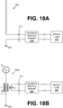
- FIGS. 18A, 18B , 18C and 19 shown are examples of generalized receive circuits for using the surface-guided waves in wireless power delivery systems.
- FIGS. 18A and 18B-18C include a linear probe 303 and a tuned resonator 306, respectively.
- FIG. 19 is a magnetic coil 309 according to various embodiments of the present disclosure.
- each one of the linear probe 303, the tuned resonator 306, and the magnetic coil 309 may be employed to receive power transmitted in the form of a guided surface wave on the surface of a lossy conducting medium 203 according to various embodiments.
- the lossy conducting medium 203 comprises a terrestrial medium (or Earth).
- the open-circuit terminal voltage at the output terminals 312 of the linear probe 303 depends upon the effective height of the linear probe 303.
- An electrical load 315 is coupled to the output terminals 312 through an impedance matching network 318.
- the electrical load 315 should be substantially impedance matched to the linear probe 303 as will be described below.
- a ground current excited coil 306a possessing a phase shift equal to the wave tilt of the guided surface wave includes a charge terminal T R that is elevated (or suspended) above the lossy conducting medium 203.
- the charge terminal T R has a self-capacitance C R .
- the bound capacitance should preferably be minimized as much as is practicable, although this may not be entirely necessary in every instance.
- the tuned resonator 306a also includes a receiver network comprising a coil L R having a phase shift ⁇ .
- One end of the coil L R is coupled to the charge terminal T R
- the other end of the coil L R is coupled to the lossy conducting medium 203.
- the receiver network can include a vertical supply line conductor that couples the coil L R to the charge terminal T R .
- the coil L R (which may also be referred to as tuned resonator L R -C R ) comprises a series-adjusted resonator as the charge terminal C R and the coil L R are situated in series.
- the phase delay of the coil L R can be adjusted by changing the size and/or height of the charge terminal T R , and/or adjusting the size of the coil L R so that the phase ⁇ of the structure is made substantially equal to the angle of the wave tilt ⁇ .
- the phase delay of the vertical supply line can also be adjusted by, e.g., changing length of the conductor.
- the reactance presented by the self-capacitance C R is calculated as 1/ j ⁇ C R .
- the total capacitance of the structure 306a may also include capacitance between the charge terminal T R and the lossy conducting medium 203, where the total capacitance of the structure 306a may be calculated from both the self-capacitance C R and any bound capacitance as can be appreciated.
- the charge terminal T R may be raised to a height so as to substantially reduce or eliminate any bound capacitance. The existence of a bound capacitance may be determined from capacitance measurements between the charge terminal T R and the lossy conducting medium 203 as previously discussed.
- the inductive reactance presented by a discrete-element coil L R may be calculated as j ⁇ L, where L is the lumped-element inductance of the coil L R . If the coil L R is a distributed element, its equivalent terminal-point inductive reactance may be determined by conventional approaches.
- To tune the structure 306a one would make adjustments so that the phase delay is equal to the wave tilt for the purpose of mode-matching to the surface waveguide at the frequency of operation. Under this condition, the receiving structure may be considered to be "mode-matched" with the surface waveguide.
- a transformer link around the structure and/or an impedance matching network 324 may be inserted between the probe and the electrical load 327 in order to couple power to the load. Inserting the impedance matching network 324 between the probe terminals 321 and the electrical load 327 can effect a conjugate-match condition for maximum power transfer to the electrical load 327.
- an electrical load 327 may be coupled to the structure 306a by way of magnetic coupling, capacitive coupling, or conductive (direct tap) coupling.
- the elements of the coupling network may be lumped components or distributed elements as can be appreciated.
- magnetic coupling is employed where a coil L S is positioned as a secondary relative to the coil L R that acts as a transformer primary.
- the coil L S may be link-coupled to the coil L R by geometrically winding it around the same core structure and adjusting the coupled magnetic flux as can be appreciated.
- the receiving structure 306a comprises a series-tuned resonator, a parallel-tuned resonator or even a distributed-element resonator of the appropriate phase delay may also be used.
- a receiving structure immersed in an electromagnetic field may couple energy from the field
- polarization-matched structures work best by maximizing the coupling, and conventional rules for probe-coupling to waveguide modes should be observed.
- a TE 20 (transverse electric mode) waveguide probe may be optimal for extracting energy from a conventional waveguide excited in the TE 20 mode.
- a mode-matched and phase-matched receiving structure can be optimized for coupling power from a surface-guided wave.
- the guided surface wave excited by a guided surface waveguide probe 200 on the surface of the lossy conducting medium 203 can be considered a waveguide mode of an open waveguide. Excluding waveguide losses, the source energy can be completely recovered.
- Useful receiving structures may be E-field coupled, H-field coupled, or surface-current excited.
- the receiving structure can be adjusted to increase or maximize coupling with the guided surface wave based upon the local characteristics of the lossy conducting medium 203 in the vicinity of the receiving structure.
- a receiving structure comprising the tuned resonator 306a of FIG. 18B , including a coil L R and a vertical supply line connected between the coil L R and a charge terminal T R .
- the charge terminal T R positioned at a defined height above the lossy conducting medium 203, the total phase shift ⁇ of the coil L R and vertical supply line can be matched with the angle ( ⁇ ) of the wave tilt at the location of the tuned resonator 306a.
- the wave tilt angle ( ⁇ ) can be determined from Equation (97).
- One or both of the phase delays ( ⁇ c + ⁇ y ) can be adjusted to match the phase shift ⁇ to the angle ( ⁇ ) of the wave tilt. For example, a tap position may be adjusted on the coil L R of FIG.
- the vertical supply line conductor can also be connected to the coil L R via a tap, whose position on the coil may be adjusted to match the total phase shift to the angle of the wave tilt.
- Z R 1 j ⁇ C R
- C R is the self-capacitance of the charge terminal T R
- the impedance seen "looking up" into the vertical supply line conductor of the tuned resonator 306a is given by:
- the coupling into the guided surface waveguide mode may be maximized.
- the tuned resonator 306b does not include a charge terminal T R at the top of the receiving structure.
- the tuned resonator 306b does not include a vertical supply line coupled between the coil L R and the charge terminal T R .
- the total phase shift ( ⁇ ) of the tuned resonator 306b includes only the phase delay ( ⁇ c ) through the coil L R .
- FIG. 18D shown is a flow chart 180 illustrating an example of adjusting a receiving structure to substantially mode-match to a guided surface waveguide mode on the surface of the lossy conducting medium 203.
- the receiving structure includes a charge terminal T R (e.g., of the tuned resonator 306a of FIG. 18B )
- the charge terminal T R is positioned at a defined height above a lossy conducting medium 203 at 184.
- the physical height ( h p ) of the charge terminal T R may be below that of the effective height.
- the physical height may be selected to reduce or minimize the bound charge on the charge terminal T R (e.g., four times the spherical diameter of the charge terminal). If the receiving structure does not include a charge terminal T R (e.g., of the tuned resonator 306b of FIG. 18C ), then the flow proceeds to 187.
- the electrical phase delay ⁇ of the receiving structure is matched to the complex wave tilt angle ⁇ defined by the local characteristics of the lossy conducting medium 203.
- the phase delay ( ⁇ c ) of the helical coil and/or the phase delay ( ⁇ y ) of the vertical supply line can be adjusted to make ⁇ equal to the angle ( ⁇ ) of the wave tilt ( W ).
- the angle ( ⁇ ) of the wave tilt can be determined from Equation (86).
- the electrical phase ⁇ can then be matched to the angle of the wave tilt.
- the load impedance of the charge terminal T R can be tuned to resonate the equivalent image plane model of the tuned resonator 306a.
- the depth (d/2) of the conducting image ground plane 139 ( FIG. 9A ) below the receiving structure can be determined using Equation (100) and the values of the lossy conducting medium 203 (e.g., the Earth) at the receiving structure, which can be locally measured.
- the impedance ( Z in ) as seen "looking down" into the lossy conducting medium 203 can then be determined using Equation (99). This resonance relationship can be considered to maximize coupling with the guided surface waves.
- the velocity factor, phase delay, and impedance of the coil L R and vertical supply line can be determined.
- the self-capacitance ( C R ) of the charge terminal T R can be determined using, e.g., Equation (24).
- the propagation factor ( ⁇ p ) of the coil L R can be determined using Equation (98), and the propagation phase constant ( ⁇ w ) for the vertical supply line can be determined using Equation (49).
- the impedance ( Z base ) of the tuned resonator 306a as seen "looking up” into the coil L R can be determined using Equations (101), (102), and (103).
- the equivalent image plane model of FIG. 9A also applies to the tuned resonator 306a of FIG. 18B .
- the impedance at the physical boundary 136 ( FIG. 9A ) "looking up" into the coil of the tuned resonator 306a is the conjugate of the impedance at the physical boundary 136 "looking down" into the lossy conducting medium 203.
- An iterative approach may be taken to tune the load impedance Z R for resonance of the equivalent image plane model with respect to the conducting image ground plane 139. In this way, the coupling of the electric field to a guided surface waveguide mode along the surface of the lossy conducting medium 203 (e.g., Earth) can be improved and/or maximized.
- the magnetic coil 309 comprises a receive circuit that is coupled through an impedance matching network 333 to an electrical load 336.
- the magnetic coil 309 may be positioned so that the magnetic flux of the guided surface wave, H ⁇ , passes through the magnetic coil 309, thereby inducing a current in the magnetic coil 309 and producing a terminal point voltage at its output terminals 330.
- ⁇ r is the effective relative permeability of the core of the magnetic coil 309
- ⁇ o is the permeability of free space
- H ⁇ is the incident magnetic field strength vector
- n ⁇ is a unit vector normal to the cross-sectional area of the turns
- a CS is the area enclosed by each loop.
- the magnetic coil 309 may be tuned to the guided surface wave frequency either as a distributed resonator or with an external capacitor across its output terminals 330, as the case may be, and then impedance-matched to an external electrical load 336 through a conjugate impedance matching network 333.
- the current induced in the magnetic coil 309 may be employed to optimally power the electrical load 336.
- the receive circuit presented by the magnetic coil 309 provides an advantage in that it does not have to be physically connected to the ground.
- the receive circuits presented by the linear probe 303, the mode-matched structure 306, and the magnetic coil 309 each facilitate receiving electrical power transmitted from any one of the embodiments of guided surface waveguide probes 200 described above.
- the energy received may be used to supply power to an electrical load 315/327/336 via a conjugate matching network as can be appreciated.
- the receive circuits presented by the linear probe 303, the mode-matched structure 306, and the magnetic coil 309 will load the excitation source 212 (e.g., FIGS. 3 , 12 and 16 ) that is applied to the guided surface waveguide probe 200, thereby generating the guided surface wave to which such receive circuits are subjected.
- the excitation source 212 e.g., FIGS. 3 , 12 and 16
- the guided surface wave generated by a given guided surface waveguide probe 200 described above comprises a transmission line mode.
- a power source that drives a radiating antenna that generates a radiated electromagnetic wave is not loaded by the receivers, regardless of the number of receivers employed.
- one or more guided surface waveguide probes 200 and one or more receive circuits in the form of the linear probe 303, the tuned mode-matched structure 306, and/or the magnetic coil 309 can make up a wireless distribution system.
- the distance of transmission of a guided surface wave using a guided surface waveguide probe 200 as set forth above depends upon the frequency, it is possible that wireless power distribution can be achieved across wide areas and even globally.
- the conventional wireless-power transmission/distribution systems extensively investigated today include "energy harvesting" from radiation fields and also sensor coupling to inductive or reactive near-fields.
- the present wireless-power system does not waste power in the form of radiation which, if not intercepted, is lost forever.
- the presently disclosed wireless-power system limited to extremely short ranges as with conventional mutual-reactance coupled near-field systems.
- the wireless-power system disclosed herein probe-couples to the novel surface-guided transmission line mode, which is equivalent to delivering power to a load by a wave-guide or a load directly wired to the distant power generator.
- FIGS. 20A-E shown are examples of various schematic symbols that are used with reference to the discussion that follows.
- a depiction of this symbol will be referred to as a guided surface waveguide probe P.
- any reference to the guided surface waveguide probe P is a reference to any one of the guided surface waveguide probes 200a, 200b, 200c, 200e, 200d, or 200f; or variations thereof.
- a symbol that represents a guided surface wave receive structure that may comprise any one of the linear probe 303 ( FIG. 18A ), the tuned resonator 306 ( FIGS. 18B-18C ), or the magnetic coil 309 ( FIG. 19 ).
- a depiction of this symbol will be referred to as a guided surface wave receive structure R.
- any reference to the guided surface wave receive structure R is a reference to any one of the linear probe 303, the tuned resonator 306, or the magnetic coil 309; or variations thereof.
- FIG. 20C shown is a symbol that specifically represents the linear probe 303 ( FIG. 18A ).
- a depiction of this symbol will be referred to as a guided surface wave receive structure R P .
- any reference to the guided surface wave receive structure R P is a reference to the linear probe 303 or variations thereof.
- FIG. 20D shown is a symbol that specifically represents the tuned resonator 306 ( FIGS. 18B-18C ).
- a depiction of this symbol will be referred to as a guided surface wave receive structure R R .
- any reference to the guided surface wave receive structure R R is a reference to the tuned resonator 306 or variations thereof.
- FIG. 20E shown is a symbol that specifically represents the magnetic coil 309 ( FIG. 19 ).
- a depiction of this symbol will be referred to as a guided surface wave receive structure R M .
- any reference to the guided surface wave receive structure R M is a reference to the magnetic coil 309 or variations thereof.
- a power service provider may sell or lease guided surface wave receive equipment to a subscriber of a guided surface wave service.
- Such guided surface wave receive equipment such as an auxiliary computing device for use in processing a guided surface wave and providing auxiliary services (e.g., authentication services), may be configured to operate with guided surface waveguide probes P, as previously discussed.
- auxiliary services e.g., authentication services
- an unauthorized sale of guided surface wave receive equipment or theft of guided surface wave receive equipment may be attempted by persons who intend to benefit from consumption of power without reimbursement to the power service provider.
- embodiments of the present disclosure can limit functioning of guided surface wave receive equipment to unauthorized users.
- FIG. 21 shown is a graphical representation of an example of a guided surface waveguide probe 2100, as represented in FIG. 14 , including modulation circuitry or application module 2110 coupled to an excitation source 212. It is understood that the guided surface waveguide probe 2100 is shown as an example to illustrate the various embodiments of the present disclosure and that other embodiments of guided surface waveguide probes described herein may be employed.
- encrypted or unencrypted valid key code data 2130 may be supplied by a guided surface wave controller device 2120 coupled to the probe 2100 and embedded with a guided surface wave using the modulation circuitry/module 2110.
- a portion of the signal V 1 applied to the coil 215 may vary in frequency, phase, and/or amplitude to convey a data signal conveying the key code data 2130.
- valid key code data 2130 may be supplied to a guided surface wave receive structure R of the subscriber of a power service as embedded data within the guided surface wave as a form of in-band communication.
- the controller device 2120 for the power service may send a user key code data 2140 to the guided surface wave receive structure R of a subscriber or authorized user in a separate out-of-band communication channel, such as a cellular transmission, Internet communication, encrypted network channel or tunnel, etc. over a network 2150.
- a separate out-of-band communication channel such as a cellular transmission, Internet communication, encrypted network channel or tunnel, etc.
- the guided surface wave receive equipment 2160 may store the received user key code 2140 in a memory area, such as, but not limited to, a reserved and protected memory area.
- a memory area such as, but not limited to, a reserved and protected memory area.
- the reserved memory area 2167 ( FIG. 22 ) is not readable by an external system or application outside of an authentication application 2163 of the guided surface wave receive equipment 2160.
- a processor 2503 ( FIG. 26 ) of the guided surface wave receive equipment 2160 only accepts read or write commands initiated by the authentication application 2163 for the reserved memory area 2167.
- the user key code 2140 may be periodically or routinely updated to new values that will be checked against the valid key code 2130 obtained from a received guided surface wave. Accordingly, in various embodiments, a subscriber or authorized user of the power service is provided updates to the user key code 2140. Therefore, a guided surface wave receive structure R of a current subscriber will have the most recently updated user key code 2140 in its reserved memory area 2167 which should be validated against the valid key code 2130 obtained from or received with the received guided surface wave, in one embodiment.
- the stored user key code 2140 is successfully validated against the valid key code 2130, functionality of the guided surface wave receive equipment 2160 is enabled and the guided surface wave receive equipment 2160 can operate to process the electrical energy provided by the guided surface wave and deliver the energy to an applied electrical load 315/527/336. Otherwise, if the stored user key code 2140 is not validated against the valid key code 2130, then functionality of the guided surface wave receive equipment 2160 is disabled to prevent the guided surface wave receive equipment 2160 from delivering electrical energy from the guided surface wave to an applied load 315/527/336. In one embodiment, a stored user key code expires after a designated period of time. Therefore, after its expiration, the stored user key code 2140 is no longer valid for use in authorization of guided surface wave receive equipment 2160.
- the respective key codes 2130, 2140 may be compared to determine if they match in one embodiment.
- a hash function h(x) may be used in some embodiments as a point of comparison to determine compatibility of key codes.
- a hash function of the valid key code 2130 may be computed and compared against the stored user key code 2140 in one embodiment of the receive equipment 2160. Accordingly, if the hash function value corresponds to the stored user key code 2140, then the user key code 2140 may be considered to be valid.
- Other authentication techniques may also be employed in various embodiments, as is known to one of ordinary skill in the art.
- the authentication control environment 2200 includes a guided surface wave controller device 2120, guided surface wave receive equipment 2160, and potentially other devices, which are in data communication with each other via a network 2150 and guided surface wave communication 2210.
- the network 2150 includes, for example, the Internet, intranets, extranets, wide area networks (WANs), local area networks (LANs), wired networks, wireless networks, or other suitable networks, etc., or any combination of two or more such networks for out-of-band signaling.
- Such networks may comprise satellite networks, cable networks, Ethernet networks, and other types of networks.
- In-band communications 2210 may also be performed between a surface waveguide probe P and a guided surface wave receive structure R using a guided surface wave. Accordingly, in-band communications 2210 may include digitally encoded data transmitted via guided surface waves between one or more guided surface wave waveguide probes P and one or more guided surface wave waveguide receive structures R.
- various network protocols such as various versions of various layer 1 and/or layer 2 protocols specified by the Open Systems Interconnection (OSI) model
- OSI Open Systems Interconnection
- Ethernet protocol or similar protocols may be adopted to facilitate transmission of digitally encoded data between guided surface wave waveguide probes P and guided surface wave waveguide receive structures R.
- Various networking techniques may also be used to manage the bandwidth provided by network 2150. For example, time-division multiplexing techniques, frequency-division multiplexing techniques, and/or other similar approaches or techniques may be used.
- the guided surface wave controller device 2120 may utilize a network interface 2124 (e.g., a network interface communication module) to send and receive messages over the network 2150.
- a network interface 2124 e.g., a network interface communication module
- the guided surface wave controller device 2120 may comprise, for example, a server computer or any other system providing computing capability.
- the controller device 2120 may employ a plurality of computing devices that may be arranged, for example, in one or more server banks or computer banks or other arrangements. Such computing devices may be located in a single installation or may be distributed among many different geographical locations.
- the controller device 2120 may include a plurality of computing devices that together may comprise a hosted computing resource, a grid computing resource and/or any other distributed computing arrangement.
- the controller device may correspond to an elastic computing resource where the allotted capacity of processing, network, storage, or other computing-related resources may vary over time.
- Various applications and/or other functionality may be executed in the guided surface wave controller device 2120 according to various embodiments, such as key generator functionality, module, or application 2126 and user authentication functionality/module/application 2128.
- the key generator 2126 is configured to create key codes to be used as either a valid key code 2140 and/or user key code 2130.
- various data may be stored in a data store 2408 ( FIG. 25 ) that is accessible to the controller device 2120.
- the data stored may include, for example, a user profile and a media access control (MAC) address of the network interface 2164 of the guided surface wave receive equipment 2160 (e.g., network interface communication module) assigned to the user, and/or other unique identifiers.
- MAC media access control
- the guided surface wave receive equipment 2160 may include, for example, any device, system, or apparatus that includes a guided surface wave receive structure R. Further, the guided surface wave receive equipment 2160 may include computing capabilities, such as a processor, a memory, and other circuitry as described herein, necessary to process authentication verification services and and/or take some action based at least in part on detection of unauthorized use of the guided surface wave receive equipment 2160.
- the guided surface wave receive structure R and computing circuitry may be integrated into the guided surface wave receive equipment 2160 or may be affixed or attached to the guided surface wave receive equipment 2160.
- the guided surface wave receive equipment 2160 may be embodied in the form of a desktop computer, a laptop computer, a set-top box, or other devices with like capability.
- the guided surface wave receive equipment 2160 may be configured to execute various applications, such as demodulation/decryption application(s) 2166, authentication application(s) 2163, and/or other applications or functionalities related to the delivery of power embodied in guided surface waves.
- the various applications may be executed by a processor 2503 ( FIG. 26 ) of the guided surface wave receive equipment 2160, for example, to perform one or more actions.
- a valid key code 2130 may be obtained from an out-of-band communication 2210 (via network interface 2163 and demodulation/decryption application or module 2166) and processed to determine if a stored user key code 2140 in reserved memory area 2167 is validated by verifying the user key code 2140 against the valid key code 2130 (e.g., determining compatibility, etc .).
- a certain amount of non-volatile memory is reserved for internal use by the authentication application 2163; and a second portion of memory 2168 is available for data storage and retrieval by the guided surface wave receive equipment 2160.
- the reserved portion 2167 of non-volatile memory comprises a user key storage area that is adapted to store a user key code 2140 therein.
- the user key code 2140 and/or valid key code 2130 may comprise a number of bytes of information, and may contain from about 8 to about 16 bytes, in one embodiment.
- the authentication application 2163 of guided surface wave receive equipment 2160 may cause functionality of the guided surface wave receive equipment 2160 related to delivery of power from a received guided surface wave to be enabled (or to be allowed to continue operation), in various embodiments. However, for an unsuccessful validation (i.e., invalidation), the authentication application 2163 may cause functionality of the guided surface wave receive equipment 2160 related to delivery of power from a received guided surface wave to be disabled.
- the guided surface wave receive structure R of the guided surface wave receive equipment 2160 receives a guided surface wave, which, in some instances, may also operate to charge or otherwise power the guided surface wave receive equipment 2160 or portions thereof. If the guided surface wave receive structure R receives the guided surface wave and detects user key code data 2140 embedded in the guided surface wave, the authentication application 2163 may then request for the user key code 2140 to be retrieved from the reserved memory area 2167 in order to determine what action, if any, should be performed in response. The authentication application 2163 may then cause certain receive functionality/circuitry 2161 to be disabled or enabled as a result of a comparison of the stored user key code 2140 with the valid key code 2130 embedded in the guided surface wave.
- a valid key code 2130 that accompanies a power signal can be used to validate a user key code 2140 obtained separately in a communication channel of the guided surface wave receive equipment 2160 in order to verify or authenticate a current user or an intended operation of the guided surface wave receive equipment 2160.
- the valid key code may be provided out-of-band concurrent with transmission of the guided surface wave (e.g., via a cellular transmission, Internet communication, encrypted network channel or tunnel, etc. over a network 2150).
- some of the data may be stored in memory 2168 or other form of data storage for the guided surface wave receive equipment 2160.
- Some examples of actions include powering off the guided surface wave receive equipment 2160, disabling certain features, functionality, or subcomponents 2161 of the guided surface wave receive equipment to avoid unauthorized use, enabling a sleep mode for certain features for a set period, etc. Accordingly, in some instances, an action may specify that a function or capability of the guided surface wave receive equipment 2160 be disabled. Further, if the pair of key codes are incompatible, access to the reserved memory area 2167 may be restricted. In some embodiments, the reserved memory area 2167 may be destroyed using various techniques including incendiary devices or other devices.
- the network interface 2164 may be configured to connect to one or more computer networks, such as the network 2150.
- the network interface 2164 may correspond to a wired or a wireless interface.
- the network interface 2164 may correspond to a Bluetooth® interface, an IEEE 802.11 wireless network (Wi-Fi®) interface, a cellular radio transmitter and receiver, or similar network interface.
- Wi-Fi® IEEE 802.11 wireless network
- the guided surface wave receive equipment 2160 may then continue to monitor for a new or updated user key code 2140 within an out-of-band communication.
- the authentication application 2163 may cause the processor 2503 ( FIG. 26 ) of the guided surface wave receive equipment 2160 to resume disabled features if an updated user key code 2140 is received and is validated against a valid key code 2130 obtained from a guided surface wave.
- the authentication application 2163 may be configured to check for an updated user key code 2140 at start-up of the guided surface wave receive equipment 2160 or at periodic intervals.
- the authentication application 2163 may be requested by corresponding user authentication application 2128 at the guided surface wave controller device 2120 for a user-ID and/or password associated with the guided surface wave receive equipment 2160. Therefore, if the user-ID and/or password information that is provided is validated by the user authentication application 2128, then an updated user key 2140 can be provided and stored in the reserved memory area 2167 in the guided surface wave receive equipment 2160.
- all or portions of the guided surface wave receive equipment 2160 may be enclosed in an external case that protects the various components of the guided surface wave receive structure R.
- the guided surface wave receive equipment 2160 may be a portable or handheld unit, with the guided surface wave receive structure R enclosed within a single shell.
- the guided surface wave receive structure R may correspond to one or more structures capable of receiving a guided surface wave.
- the guided surface wave receive structure R may include, for example, a linear probe, a tuned resonator, a magnetic coil, and/or similar structures for receiving a guided surface wave, as previously described above.
- the guided surface wave receive structure R may represent a plurality of guided surface wave receive structures R, each of which is tuned to receive a guided surface wave on a different frequency from the other guided surface wave receive structures R.
- the guided surface wave receive structure R may be configured to be tuned to receive multiple guided surface waves on different frequencies simultaneously.
- the guided surface wave receive structure R may be configured to alternate frequencies in order to detect, receive, and/or measure a guided surface wave on a first frequency and then switch to a second frequency to detect a second guided surface wave on a second frequency.
- a network interface 2124 at a guided surface wave controller device 2120 associated with a guided surface waveguide probe can transmit a user key code 2140 to guided surface wave receive equipment 2160 associated with the user (e.g., a current subscriber to a guided surface wave service).
- the user key code 2140 can be transmitted (2310) over a network 2150 to a network interface 2164 of the guided surface wave receive equipment 2160 associated with the user.
- the user key code 2140 may be stored (2320) in a reserved and protected area of memory 2167 for the guided surface wave receive equipment 2160 for subsequent retrieval and processing.
- modulation circuitry or application module 2110 coupled to the guided surface waveguide probe P can embed a valid key code with a guided surface wave that is launched or transmitted (2330) across a lossy medium, such as a terrestrial medium, to the guided surface wave receive equipment 2160.
- the valid key code 2130 may also be provided to a known or authorized guided surface wave receive equipment 2160.
- the valid key 2160 may be transmitted in an out-of-band communication to the guided surface wave receive equipment 2160 whose associated user account is in good status and not transmitted to a guided surface wave receive equipment 2160 that is deficient in paying for past services (e.g., its user account is in a bad status).
- a demodulator component or circuitry 2166 at the guided surface wave receive equipment 2160 can process the power signal to determine the valid key code 2130.
- the valid key code 2130 may then be stored (2340) in memory 2168 or cache to await further processing by an authentication application 2163 of the guided surface wave receive equipment 2160.
- the authentication application 2163 is adapted to retrieve the user key code 2140 stored in reserved memory 2167 with the valid key code 2130 to determine (2350) if the respective key codes are compatible (e.g., correspond to the same value or function). If the respective key codes are compatible, then functionality 2161 of the guided surface wave receive equipment 2160 is enabled (2170) or maintained to allow for delivery of electrical energy obtained from the guided surface wave to an electrical load 315/527/336 coupled to the guided surface wave receive structure R. For example, certain equipment components or features may be activated.
- functionality 2161 of the guided surface wave receive equipment 2160 is disabled (2180) or deactivated to prohibit/restrict delivery of electrical energy obtained from the guided surface wave to the electrical load 315/527/336 coupled to the guided surface wave receive structure R.
- a reserved memory area 2167 may maintain a unique identification number for the guided surface wave receive equipment 2160 and/or user, such as a serial number S/N, a device identification number, a user account number, a secret identification number, etc. Accordingly, as part of an authentication process, the guided surface wave receive equipment 2160 may transmit such a serial number S/N to the guided surface wave controller device 2120 associated with a guided surface waveguide probe (from the network interface 2164 of the receive equipment 2160 to the network interface 2124 of the controller device 2120 over a network 2150).
- the transmission may be made as part of a secure network tunnel communication or other type of secured communication, in one embodiment.
- a user authentication application 2128 at the guided surface wave controller device 2120 can perform an authentication validation process to determine if the serial number S/N received from the guided surface wave receive equipment 2160 is validated or authorized to received guided surface wave transmissions. Accordingly, at 2380, if the guided surface wave receive equipment 2160 is validated, then the user authentication application 2128 can send an enable command (over network 2150 to network interface 2124 of a controller device 2120) to the receive equipment 2160 (such as functionality circuit 2160 and/or processor 2503 ( FIG. 26 )) to enable operation of the guided surface wave receive equipment 2160.
- an enable command over network 2150 to network interface 2124 of a controller device 2120
- the user authentication application 2128 can send (over network 2150 to network interface 2124 of a controller device 2120) a disable command to the receive equipment 2160 (such as functionality circuit 2160 and/or processor 2503 ( FIG. 26 )) to disable operation of the guided surface wave receive equipment 2160.
- a disable command to the receive equipment 2160 (such as functionality circuit 2160 and/or processor 2503 ( FIG. 26 )) to disable operation of the guided surface wave receive equipment 2160.
- functionality 2161 of the guided surface wave receive equipment 2160 Upon receipt of an enable command, functionality 2161 of the guided surface wave receive equipment 2160 is enabled or maintained to allow for delivery of electrical energy obtained from the guided surface wave to an electrical load 315/527/336 coupled to the guided surface wave receive structure R. For example, certain equipment components or features may be activated. On the other hand, upon receipt of a disable command, functionality 2161 of the guided surface wave receive equipment 2160 is disabled or deactivated to prohibit/restrict delivery of electrical energy obtained from the guided surface wave to the electrical load 315/527/336 coupled to the guided surface wave receive structure R.
- FIG. 24 shown is a flowchart that provides one example of the operation of a portion of the guided surface wave receive equipment 2160 according to various embodiments. It is understood that the flowchart of FIG. 24 provides merely an example of the many different types of functional arrangements that may be employed to implement the operation of the portion of the guided surface wave receive equipment 2160 (e.g., authentication application 2163) as described herein. As an alternative, the flowchart of FIG. 24 may be viewed as depicting an example of elements of a method implemented in the guided surface wave receive equipment 2160 ( FIG. 22 ) according to various embodiments.
- the guided surface wave receive equipment 2160 determines whether a guided surface wave receive structure R has received a guided surface wave. If guided surface wave receive equipment 2160 determines that the guided surface wave receive structure R is not currently receiving a guided surface wave or has not received the guided surface wave, then execution of the process skips to box 2313. However, if the guided surface wave receive structure R has received the guided surface wave, then execution of the process proceeds to box 2306.
- the guided surface wave receive equipment 2160 causes a processor 2503 ( FIG. 26 ) of the guided surface wave receive equipment 2160 to decode or demodulate a valid key code 2130 embedded or otherwise encoded in the guided surface wave, if present.
- the valid key code 2130 may be sent in an out-of-band communication to the guided surface wave receive equipment 2160.
- the valid key code 2130 may be used by authentication application 2163 to validate a user key code 2140 stored in reserved memory 2167 of the guided surface wave receive equipment 2160.
- the user authentication application 2163 causes the processor 2503 ( FIG. 26 ) of the guided surface wave receive equipment 2160 to retrieve the user key from the reserved memory area 2167. The authentication application 2163 then determines what action, if any, should be performed in response to comparing the valid key code 2130 with the user key code 2140. Execution proceeds to box 2311.
- the guided surface wave receive equipment 2160 may be configured to poll or pull the user authentication application 2128 at the guided surface wave controller device 2120 at a scheduled time/interval for an updated user key code 2140.
- the user authentication application 2128 at the guided surface wave controller device 2120 may push an updated user key code 2140 to the guided surface wave receive equipment 2160 at a registered MAC address for the guided surface wave receive equipment 2160.
- a stored user key code 2140 at the guided surface wave receive equipment 2160 may be considered to be expired by the guided surface wave receive equipment 2160, and the guided surface wave receive equipment 2160 may be configured to request a new updated user key code 2140 from the controller device 2120.
- the controller device 2120 may provide an updated key code 2140 upon verification that the guided surface wave receive equipment 2160 is associated with a valid user-ID and/or password.
- the guided surface wave receive equipment 2160 may request a new updated user key code 2140 from the guided surface wave controller device 2120 upon notification from the authorization application 2163 that a stored user key code is incompatible with a valid key code 2130.
- the authentication application 2163 causes the processor 2503 ( FIG. 26 ) of guided surface wave receive equipment 2160 to perform the action specified by the authentication application 2163.
- the authentication application 2163 may cause the processor 2503 ( FIG. 26 ) to disable functionality 2161 (e.g., disable one or more components) of the guided surface wave receive equipment 2160 if the user key code 2140 is incompatible or correspond to the valid key code 2130. Otherwise, the authentication application 2163 may cause the processor 2503 ( FIG.
- functionality 2161 e.g., one or more components
- the authentication application 2163 may also, in some embodiments, cause dedicated action circuitry to perform such actions instead of the processor 2503 ( FIG. 26 ). Although use of the processor 2503 ( FIG. 26 ) to perform one or more of these actions with software may simplify the manufacture of the guided surface wave receive equipment 2160, the use of dedicate hardware, to perform actions may be more secure. After the appropriate action is performed, execution of the process ends (at block 2313).
- the controller device 2120 may include at least one processor circuit, for example, having a processor 2402 and a memory 2404, both of which are coupled to a local interface 2406.
- the local interface 2406 may comprise, for example, a data bus with an accompanying address/control bus or other bus structure as can be appreciated.
- Stored in the memory 2404 are both data and several components that are executable by the processor 2402.
- stored in the memory 2404 and executable by the processor 2402 are the user authentication application 2128, and potentially other applications.
- Also stored in the memory 2404 may be a data store 2408 and other data.
- an operating system may be stored in the memory 2404 and executable by the processor 2402.
- any one of a number of programming languages may be employed such as, for example, C, C++, C#, Objective C, Java®, JavaScript®, Perl, PHP, Visual Basic®, Python®, Ruby, Flash®, or other programming languages.
- executable means a program file that is in a form that can ultimately be run by the processor 2402.
- Examples of executable programs may be, for example, a compiled program that can be translated into machine code in a format that can be loaded into a random access portion of the memory 2404 and run by the processor 2402, source code that may be expressed in proper format such as object code that is capable of being loaded into a random access portion of the memory 2404 and executed by the processor 2402, or source code that may be interpreted by another executable program to generate instructions in a random access portion of the memory 2404 to be executed by the processor 2402, etc.
- An executable program may be stored in any portion or component of the memory 2404 including, for example, random access memory (RAM), read-only memory (ROM), hard drive, solid-state drive, USB flash drive, memory card, optical disc such as compact disc (CD) or digital versatile disc (DVD), floppy disk, magnetic tape, a Flash or Programmable Read Only Memory chip, or other memory components.
- RAM random access memory
- ROM read-only memory
- hard drive solid-state drive
- USB flash drive memory card
- optical disc such as compact disc (CD) or digital versatile disc (DVD)
- floppy disk magnetic tape
- Flash or Programmable Read Only Memory chip or other memory components.
- the guided surface wave receive equipment 2160 may include at least one processor circuit, for example, having a processor 2503 and a memory 2168, both of which are coupled to a local interface 2509.
- the local interface 2509 may comprise, for example, a data bus with an accompanying address/control bus or other bus structure as can be appreciated.
- Stored in the memory 2168 are both data and several components that are executable by the processor 2503.
- stored in the memory 2168 and executable by the processor 2503 are the authentication application 2163, and potentially other applications.
- Also stored in the memory 2168 may be a data store 2167 (e.g., reserved memory area) and other data or data storage areas, such as a cache.
- an operating system may be stored in the memory 2168 and executable by the processor 2503.
- any one of a number of programming languages may be employed such as, for example, C, C++, C#, Objective C, Java®, JavaScript®, Perl, PHP, Visual Basic®, Python®, Ruby, Flash®, or other programming languages.
- executable means a program file that is in a form that can ultimately be run by the processor 2503.
- executable programs may be, for example, a compiled program that can be translated into machine code in a format that can be loaded into a random access portion of the memory 2168 and run by the processor 2503, source code that may be expressed in proper format such as object code that is capable of being loaded into a random access portion of the memory 2168 and executed by the processor 2503, or source code that may be interpreted by another executable program to generate instructions in a random access portion of the memory 2168 to be executed by the processor 2503, etc.
- An executable program may be stored in any portion or component of the memory 2168 including, for example, random access memory (RAM), read-only memory (ROM), hard drive, solid-state drive, USB flash drive, memory card, optical disc such as compact disc (CD) or digital versatile disc (DVD), floppy disk, magnetic tape, or other memory components, including protected and reserved memory areas.
- RAM random access memory
- ROM read-only memory
- hard drive solid-state drive
- USB flash drive Universal Serial Bus flash drive
- memory card such as compact disc (CD) or digital versatile disc (DVD), floppy disk, magnetic tape, or other memory components, including protected and reserved memory areas.
- CD compact disc
- DVD digital versatile disc
- memory 2168 and memory 2404 are defined herein as including both volatile and nonvolatile memory and data storage components. Volatile components are those that do not retain data values upon loss of power. Nonvolatile components are those that retain data upon a loss of power.
- memory 2168 and memory 2404 may comprise, for example, random access memory (RAM), read-only memory (ROM), hard disk drives, solid-state drives, USB flash drives, memory cards accessed via a memory card reader, floppy disks accessed via an associated floppy disk drive, optical discs accessed via an optical disc drive, magnetic tapes accessed via an appropriate tape drive, and/or other memory components, or a combination of any two or more of these memory components.
- the RAM may comprise, for example, static random access memory (SRAM), dynamic random access memory (DRAM), or magnetic random access memory (MRAM) and other such devices.
- the ROM may comprise, for example, a programmable read-only memory (PROM), an erasable programmable read-only memory (EPROM), an electrically erasable programmable read-only memory (EEPROM), or other like memory device.
- processor 2503 and processor 2402 may represent multiple processors and/or multiple processor cores and the memory 2168, 2404 may represent multiple memories that operate in parallel processing circuits, respectively.
- the local interface 2509, 2609 may be an appropriate network that facilitates communication between any two of the multiple processors 2503, 2402, between any processor 2503, 2402 and any of the memories 2168, 2404, or between any two of the memories 2168, 2404, etc.
- the local interface 2509, 2609 may comprise additional systems designed to coordinate this communication, including, for example, performing load balancing.
- the processor 2503, 2402 may be of electrical or of some other available construction.
- user authentication application 2128 may be embodied in software or code executed by general purpose hardware as discussed above, as an alternative the same may also be embodied in dedicated hardware or a combination of software/general purpose hardware and dedicated hardware. If embodied in dedicated hardware, each can be implemented as a circuit or state machine that employs any one of or a combination of a number of technologies. These technologies may include, but are not limited to, discrete logic circuits having logic gates for implementing various logic functions upon an application of one or more data signals, application specific integrated circuits (ASICs) having appropriate logic gates, field-programmable gate arrays (FPGAs), or other components, etc. Such technologies are generally well known by those skilled in the art and, consequently, are not described in detail herein.
- FIGS. 23 and 24 show a specific order of execution, it is understood that the order of execution may differ from that which is depicted. For example, the order of execution of two or more blocks may be scrambled relative to the order shown. Also, two or more blocks shown in succession in FIGS. 23 and 24 may be executed concurrently or with partial concurrence. Further, in some embodiments, one or more of the blocks shown in FIGS. 23 and 24 may be skipped or omitted. In addition, any number of counters, state variables, warning semaphores, or messages might be added to the logical flow described herein, for purposes of enhanced utility, accounting, performance measurement, or providing troubleshooting aids, etc. It is understood that all such variations are within the scope of the present disclosure.
- any logic or application described herein, including the user authentication application 2128 and the authentication application 2163, that comprises software or code can be embodied in any non-transitory computer-readable medium for use by or in connection with an instruction execution system such as, for example, a processor in a computer system or other system.
- the logic may comprise, for example, statements including instructions and declarations that can be fetched from the computer-readable medium and executed by the instruction execution system.
- a "computer-readable medium" can be any medium that can contain, store, or maintain the logic or application described herein for use by or in connection with the instruction execution system.
- the computer-readable medium can comprise any one of many physical media such as, for example, magnetic, optical, or semiconductor media. More specific examples of a suitable computer-readable medium would include, but are not limited to, magnetic tapes, magnetic floppy diskettes, magnetic hard drives, memory cards, solid-state drives, USB flash drives, or optical discs. Also, the computer-readable medium may be a random access memory (RAM) including, for example, static random access memory (SRAM) and dynamic random access memory (DRAM), or magnetic random access memory (MRAM).
- RAM random access memory
- SRAM static random access memory
- DRAM dynamic random access memory
- MRAM magnetic random access memory
- the computer-readable medium may be a read-only memory (ROM), a programmable read-only memory (PROM), an erasable programmable read-only memory (EPROM), an electrically erasable programmable read-only memory (EEPROM), or other type of memory device.
- ROM read-only memory
- PROM programmable read-only memory
- EPROM erasable programmable read-only memory
- EEPROM electrically erasable programmable read-only memory
- any logic or application described herein including the user authentication application 2128 and the authentication application 2163, may be implemented and structured in a variety of ways.
- one or more applications described may be implemented as modules or components of a single application.
- one or more applications described herein may be executed in shared or separate computing devices or a combination thereof.
- a plurality of the applications described herein may execute in the same computing device, in multiple computing devices in the same computing environment, or in the same user device.
- terms such as “application,” “service,” “system,” “engine,” “module,” and so on may be interchangeable and are not intended to be limiting.
Landscapes
- Engineering & Computer Science (AREA)
- Computer Networks & Wireless Communication (AREA)
- Power Engineering (AREA)
- Aerials With Secondary Devices (AREA)
- Variable-Direction Aerials And Aerial Arrays (AREA)
- Waveguides (AREA)
- Waveguide Aerials (AREA)
- Lock And Its Accessories (AREA)
- Charge And Discharge Circuits For Batteries Or The Like (AREA)
Applications Claiming Priority (2)
| Application Number | Priority Date | Filing Date | Title |
|---|---|---|---|
| US14/849,944 US10312747B2 (en) | 2015-09-10 | 2015-09-10 | Authentication to enable/disable guided surface wave receive equipment |
| PCT/US2016/047673 WO2017044285A1 (en) | 2015-09-10 | 2016-08-19 | Authentication to enable/disable guided surface wave receive equipment |
Publications (2)
| Publication Number | Publication Date |
|---|---|
| EP3342027A1 EP3342027A1 (en) | 2018-07-04 |
| EP3342027B1 true EP3342027B1 (en) | 2019-07-31 |
Family
ID=56855817
Family Applications (1)
| Application Number | Title | Priority Date | Filing Date |
|---|---|---|---|
| EP16760606.0A Not-in-force EP3342027B1 (en) | 2015-09-10 | 2016-08-19 | Authentication to enable/disable guided surface wave receive equipment |
Country Status (9)
| Country | Link |
|---|---|
| US (1) | US10312747B2 (https=) |
| EP (1) | EP3342027B1 (https=) |
| JP (1) | JP2018536370A (https=) |
| KR (1) | KR20180052670A (https=) |
| CN (1) | CN108352731A (https=) |
| EA (1) | EA201890686A1 (https=) |
| HK (1) | HK1253358A1 (https=) |
| TW (1) | TW201711410A (https=) |
| WO (1) | WO2017044285A1 (https=) |
Families Citing this family (6)
| Publication number | Priority date | Publication date | Assignee | Title |
|---|---|---|---|---|
| US10694379B2 (en) * | 2016-12-06 | 2020-06-23 | At&T Intellectual Property I, L.P. | Waveguide system with device-based authentication and methods for use therewith |
| US10764762B2 (en) * | 2017-10-04 | 2020-09-01 | At&T Intellectual Property I, L.P. | Apparatus and methods for distributing a communication signal obtained from ultra-wideband electromagnetic waves |
| CN109344456B (zh) * | 2018-09-11 | 2023-04-18 | 西安空间无线电技术研究所 | 一种高集成度子阵的相位补偿及验证方法 |
| CN109474935B8 (zh) * | 2018-11-28 | 2022-05-27 | 中科凯普(北京)导航通信技术有限公司 | 一种隧道微波通信传输系统及方法 |
| KR102709993B1 (ko) | 2019-02-19 | 2024-09-26 | 삼성전자 주식회사 | 무선 충전을 위한 데이터 통신 방법 및 이를 사용하는 전자 장치 |
| CN113449324B (zh) * | 2021-07-23 | 2022-05-17 | 福州博峰智能电器有限公司 | 一种电场感应式高电压智能电压测量仪表 |
Family Cites Families (163)
| Publication number | Priority date | Publication date | Assignee | Title |
|---|---|---|---|---|
| US3123767A (en) | 1964-03-03 | Uator | ||
| GB189620981A (en) | 1896-09-22 | 1896-11-21 | Nikola Tesla | Improvements relating to the Production, Regulation, and Utilization of Electric Currents of High Frequency, and to Apparatus therefor. |
| US645576A (en) | 1897-09-02 | 1900-03-20 | Nikola Tesla | System of transmission of electrical energy. |
| US685955A (en) | 1899-06-24 | 1901-11-05 | Nikola Tesla | Apparatus for utilizing effects transmitted from a distance to a receiving device through natural media. |
| US685953A (en) | 1899-06-24 | 1901-11-05 | Nikola Tesla | Method of intensifying and utilizing effects transmitted through natural media. |
| US685956A (en) | 1899-08-01 | 1901-11-05 | Nikola Tesla | Apparatus for utilizing effects transmitted through natural media. |
| US685954A (en) | 1899-08-01 | 1901-11-05 | Nikola Tesla | Method of utilizing effects transmitted through natural media. |
| US685012A (en) | 1900-03-21 | 1901-10-22 | Nikola Tesla | Means for increasing the intensity of electrical oscillations. |
| US787412A (en) | 1900-05-16 | 1905-04-18 | Nikola Tesla | Art of transmitting electrical energy through the natural mediums. |
| US725605A (en) | 1900-07-16 | 1903-04-14 | Nikola Tesla | System of signaling. |
| GB190111293A (en) | 1901-06-01 | 1901-11-02 | Nikola Tesla | Improvements relating to the Utilization of Electromagnetic, Light, or other like Radiations Effects or Disturbances transmitted through the Natural Media and to Apparatus therefor. |
| GB190113563A (en) | 1901-07-03 | 1901-11-09 | Nikola Tesla | Improvements in, and relating to, the Transmission of Electrical Energy. |
| GB190114579A (en) | 1901-07-17 | 1902-04-24 | Nikola Tesla | Improvements in and relating to the Transmission of Electrical Energy. |
| GB190508200A (en) | 1905-04-17 | 1906-04-17 | Nikola Tesla | Improvements relating to the Transmission of Electrical Energy. |
| US851336A (en) | 1905-06-27 | 1907-04-23 | Georg Von Arco | Transmitter for wireless telegraphy. |
| US1119732A (en) | 1907-05-04 | 1914-12-01 | Nikola Tesla | Apparatus for transmitting electrical energy. |
| US1452849A (en) | 1921-12-13 | 1923-04-24 | Rca Corp | Wireless transmitting station |
| US1691338A (en) | 1923-10-05 | 1928-11-13 | Westinghouse Electric & Mfg Co | Aerial system |
| US1652516A (en) | 1924-12-23 | 1927-12-13 | Westinghouse Electric & Mfg Co | Radio transmitting system |
| US1947256A (en) | 1930-01-11 | 1934-02-13 | Bell Telephone Labor Inc | Antenna counterpoise system |
| BE554252A (https=) | 1950-03-21 | |||
| US2921277A (en) | 1956-07-13 | 1960-01-12 | Surface Conduction Inc | Launching and receiving of surface waves |
| US3219954A (en) | 1957-05-31 | 1965-11-23 | Giovanni P Rutelli | Surface wave transmission system for telecommunication and power transmission |
| FR1604503A (https=) | 1960-05-31 | 1971-11-29 | ||
| US3582838A (en) | 1966-09-27 | 1971-06-01 | Zenith Radio Corp | Surface wave devices |
| US3445844A (en) | 1968-01-11 | 1969-05-20 | Raytheon Co | Trapped electromagnetic radiation communications system |
| US3742511A (en) | 1971-06-15 | 1973-06-26 | Smith Electronics Inc | Low-loss antenna system with counterpoise insulated from earth |
| US3742509A (en) | 1971-11-11 | 1973-06-26 | Raytheon Co | Subsurface traveling wave antenna |
| GB1471860A (en) | 1974-07-02 | 1977-04-27 | Plessey Co Ltd | Radio antenna incorporating low-loss high relative permittivity dielectric material |
| US4751515A (en) | 1980-07-09 | 1988-06-14 | Corum James F | Electromagnetic structure and method |
| US4808950A (en) | 1986-10-06 | 1989-02-28 | Sanders Associates, Inc. | Electromagnetic dispersive delay line |
| GB8802204D0 (en) | 1988-02-02 | 1988-03-02 | Hately M C | Twin feeder crossed field antenna systems |
| IL89468A (en) | 1989-03-03 | 1994-08-26 | Gamzon Eliyahu | Method and system for supporting an airborne vehicle in space |
| US5173690A (en) * | 1990-02-23 | 1992-12-22 | Viz Manufacturing Company | Passive ranging system utilizing range tone signals |
| US5045825A (en) | 1990-07-05 | 1991-09-03 | Hewlett-Packard Company | Coupling port for multiple capacitor, distributed inductor resonator |
| US5293308A (en) | 1991-03-26 | 1994-03-08 | Auckland Uniservices Limited | Inductive power distribution system |
| US5301096A (en) | 1991-09-27 | 1994-04-05 | Electric Power Research Institute | Submersible contactless power delivery system |
| EP0619906B1 (de) | 1992-01-03 | 1996-03-20 | Siemens Aktiengesellschaft | Passiver oberflächenwellen-sensor, der drahtlos abfragbar ist |
| US6104107A (en) | 1992-05-08 | 2000-08-15 | Uniline Limited | Method and apparatus for single line electrical transmission |
| US6075498A (en) | 1993-01-08 | 2000-06-13 | American Nucleonics Corp. | Surface wave directional detection system and method |
| JPH06225481A (ja) | 1993-01-21 | 1994-08-12 | Takeo Oe | 水中電気機器用の無線方式電力供給装置 |
| GB2288914A (en) | 1994-04-26 | 1995-11-01 | Maurice Clifford Hately | Radio antenna |
| US5835067A (en) | 1994-04-28 | 1998-11-10 | Goodman; Edward A. | Short vertical 160 meter band antenna |
| US5714917A (en) | 1996-10-02 | 1998-02-03 | Nokia Mobile Phones Limited | Device incorporating a tunable thin film bulk acoustic resonator for performing amplitude and phase modulation |
| US5920261A (en) | 1996-12-31 | 1999-07-06 | Design Vision Inc. | Methods and apparatus for tracking and displaying objects |
| US6275143B1 (en) * | 1997-05-09 | 2001-08-14 | Anatoli Stobbe | Security device having wireless energy transmission |
| KR100216885B1 (ko) | 1997-07-25 | 1999-09-01 | 윤덕용 | 전기장 센서 |
| ES2278417T3 (es) | 1997-08-08 | 2007-08-01 | Jurgen G. Meins | Metodo y aparato para suministrar energia sin contacto. |
| GB9718311D0 (en) | 1997-08-30 | 1997-11-05 | Hately Maurice C | Dual loop radio antenna |
| RU2143775C1 (ru) | 1999-03-25 | 1999-12-27 | Стребков Дмитрий Семенович | Способ и устройство для передачи электрической энергии |
| RU2161850C1 (ru) | 1999-07-14 | 2001-01-10 | Стребков Дмитрий Семенович | Способ и устройство передачи электрической энергии |
| NZ526201A (en) * | 1999-10-22 | 2004-11-26 | Nextnet Wireless Inc | Fixed OFDM wireless man utilizing CPE having internal antenna |
| US6864849B2 (en) | 2000-05-23 | 2005-03-08 | Robert T. Hart | Method and apparatus for creating an EH antenna |
| US6486846B1 (en) | 2000-05-23 | 2002-11-26 | Robert T. Hart | E H antenna |
| RU2183376C2 (ru) | 2000-07-03 | 2002-06-10 | Стребков Дмитрий Семенович | Способ и устройство для передачи электрической энергии (варианты) |
| US6650556B2 (en) | 2001-10-31 | 2003-11-18 | Intel Corporation | Multi-phase DC—DC converter |
| WO2003090309A2 (en) | 2002-04-13 | 2003-10-30 | Maurice Clifford Hately | Crossed-field radio antenna |
| RU2255406C2 (ru) | 2003-02-21 | 2005-06-27 | Государственное научное учреждение Всероссийский научно-исследовательский институт электрификации сельского хозяйства (ГНУ ВИЭСХ) | Способ и устройство для передачи электрической энергии |
| US7068234B2 (en) | 2003-05-12 | 2006-06-27 | Hrl Laboratories, Llc | Meta-element antenna and array |
| JP3924263B2 (ja) | 2003-06-09 | 2007-06-06 | ジーイー・メディカル・システムズ・グローバル・テクノロジー・カンパニー・エルエルシー | 超音波診断装置 |
| US6956535B2 (en) | 2003-06-30 | 2005-10-18 | Hart Robert T | Coaxial inductor and dipole EH antenna |
| US7280033B2 (en) | 2003-10-15 | 2007-10-09 | Current Technologies, Llc | Surface wave power line communications system and method |
| US7834813B2 (en) | 2004-10-15 | 2010-11-16 | Skycross, Inc. | Methods and apparatuses for adaptively controlling antenna parameters to enhance efficiency and maintain antenna size compactness |
| RU2273939C1 (ru) | 2004-12-01 | 2006-04-10 | Государственное научное учреждение Всероссийский научно-исследовательский институт электрификации сельского хозяйства (ГНУ ВИЭСХ) | Способ и устройство для передачи электрической энергии |
| EP1825282B1 (en) | 2004-12-13 | 2009-12-09 | inTEST Corporation | Signal module with reduced reflections |
| US9118216B2 (en) | 2005-02-18 | 2015-08-25 | Cpg Technologies, Llc | Parametric power multiplication |
| US7825543B2 (en) | 2005-07-12 | 2010-11-02 | Massachusetts Institute Of Technology | Wireless energy transfer |
| KR101118710B1 (ko) | 2005-07-12 | 2012-03-13 | 메사추세츠 인스티튜트 오브 테크놀로지 | 무선 비-방사성 에너지 전달 |
| US20070021140A1 (en) * | 2005-07-22 | 2007-01-25 | Keyes Marion A Iv | Wireless power transmission systems and methods |
| US7586384B2 (en) | 2005-08-15 | 2009-09-08 | Nokia Corporation | Integrated load impedance sensing for tunable matching networks |
| US7307589B1 (en) | 2005-12-29 | 2007-12-11 | Hrl Laboratories, Llc | Large-scale adaptive surface sensor arrays |
| RU2310964C1 (ru) | 2006-02-10 | 2007-11-20 | Российская Академия сельскохозяйственных наук Государственное научное учреждение Всероссийский научно-исследовательский институт электрификации сельского хозяйства (ГНУ ВИЭСХ РОССЕЛЬХОЗАКАДЕМИИ) | Способ и устройство для передачи электрической энергии |
| JP4278061B2 (ja) | 2006-03-06 | 2009-06-10 | 国立大学法人京都大学 | 建物内無線電力伝送システム |
| US7782264B1 (en) | 2006-03-28 | 2010-08-24 | The Board Of Governors For Higher Education, State Of Rhode Island And Providence Plantations | Systems and methods for providing distributed load monopole antenna systems |
| US7929908B2 (en) * | 2006-05-24 | 2011-04-19 | The Boeing Company | Method and system for controlling a network for power beam transmission |
| EP2027705A2 (en) | 2006-06-14 | 2009-02-25 | Powercast Corporation | Wireless power transmission |
| RU2341860C2 (ru) | 2006-07-04 | 2008-12-20 | Виктор Иванович Петрик | Способ и устройство для передачи электрической энергии (варианты) |
| CN101145810B (zh) * | 2006-09-11 | 2011-06-15 | 索尼株式会社 | 通信系统以及通信装置 |
| JP4893483B2 (ja) | 2006-09-11 | 2012-03-07 | ソニー株式会社 | 通信システム |
| JP4345850B2 (ja) | 2006-09-11 | 2009-10-14 | ソニー株式会社 | 通信システム及び通信装置 |
| US7960870B2 (en) | 2006-11-27 | 2011-06-14 | Xslent Energy Technologies, Llc | Power extractor for impedance matching |
| EP1965223B1 (en) | 2007-03-02 | 2013-12-18 | Saab Ab | Subsurface Imaging radar |
| RU2340064C1 (ru) | 2007-03-29 | 2008-11-27 | Российская Академия сельскохозяйственных наук Государственное научное учреждение Всероссийский научно-исследовательский институт электрификации сельского хозяйства (ГНУ ВИЭСХ РОССЕЛЬХОЗАКАДЕМИИ) | Способ и устройство для передачи электрической энергии (варианты) |
| RU2342761C1 (ru) | 2007-09-07 | 2008-12-27 | Российская Академия сельскохозяйственных наук Государственное научное учреждение Всероссийский научно-исследовательский институт электрификации сельского хозяйства (ГНУ ВИЭСХ РОССЕЛЬХОЗАКАДЕМИИ) | Способ и устройство для передачи электрической энергии (варианты) |
| WO2009042214A1 (en) | 2007-09-26 | 2009-04-02 | Governing Dynamics, Llc | Self-charging electric vehicles and aircraft, and wireless energy distribution system |
| US7957533B2 (en) * | 2007-10-02 | 2011-06-07 | Alcatel-Lucent Usa Inc. | Method of establishing authentication keys and secure wireless communication |
| US8350769B1 (en) | 2008-03-20 | 2013-01-08 | United States Of America As Represented By Secretary Of The Navy | Frequency agile electrically small tactical AM broadcast band antenna system |
| RU2366057C1 (ru) | 2008-04-25 | 2009-08-27 | Российская Академия сельскохозяйственных наук Государственное учреждение Всероссийский научно-исследовательский институт электрификации сельского хозяйства (ГНУ ВИЭСХ РОССЕЛЬХОЗАКАДЕМИИ) | Способ и устройство передачи электроэнергии |
| US20110050164A1 (en) * | 2008-05-07 | 2011-03-03 | Afshin Partovi | System and methods for inductive charging, and improvements and uses thereof |
| WO2009140506A1 (en) | 2008-05-14 | 2009-11-19 | Massachusetts Institute Of Technology | Wireless energy transfer, including interference enhancement |
| RU2366058C1 (ru) | 2008-05-16 | 2009-08-27 | Российская Академия сельскохозяйственных наук Государственное научное учреждение Всероссийский научно-исследовательский институт электрификации сельского хозяйства (ГНУ ВИЭСХ РОССЕЛЬХОЗАКАДЕМИИ) | Способ и устройство для передачи электроэнергии |
| EP2329290A1 (en) | 2008-08-20 | 2011-06-08 | BAE Systems PLC | High frequency surfacewave radar |
| US20110156494A1 (en) | 2008-08-25 | 2011-06-30 | Governing Dynamics Llc | Wireless Energy Transfer System |
| JP4911148B2 (ja) | 2008-09-02 | 2012-04-04 | ソニー株式会社 | 非接触給電装置 |
| US8933594B2 (en) | 2008-09-27 | 2015-01-13 | Witricity Corporation | Wireless energy transfer for vehicles |
| US8299936B2 (en) | 2008-12-18 | 2012-10-30 | Bae Systems Information And Electronic Systems Integration Inc. | Method and apparatus for establishing low frequency/ultra low frequency and very low frequency communications |
| US9130394B2 (en) | 2009-02-05 | 2015-09-08 | Qualcomm Incorporated | Wireless power for charging devices |
| JP4752931B2 (ja) | 2009-02-18 | 2011-08-17 | ブラザー工業株式会社 | 無線タグ通信装置 |
| US8338991B2 (en) | 2009-03-20 | 2012-12-25 | Qualcomm Incorporated | Adaptive impedance tuning in wireless power transmission |
| US8803474B2 (en) | 2009-03-25 | 2014-08-12 | Qualcomm Incorporated | Optimization of wireless power devices |
| US8237313B2 (en) | 2009-04-08 | 2012-08-07 | John Ruocco | Method and apparatus for wireless transmission and reception of electric power |
| TWI520439B (zh) | 2009-04-13 | 2016-02-01 | 凡爾賽特公司 | 半雙工相位陣列天線系統 |
| WO2010129369A2 (en) | 2009-04-28 | 2010-11-11 | Mojo Mobility, Inc. | System and methods for inductive charging, and improvements and uses thereof |
| JP5355783B2 (ja) | 2009-05-07 | 2013-11-27 | テレコム・イタリア・エッセ・ピー・アー | エネルギーをワイヤレスに伝達するシステム |
| US8274178B2 (en) | 2009-06-21 | 2012-09-25 | Christopher Allen Tucker | System of transmission of wireless energy |
| US8063717B2 (en) | 2009-07-27 | 2011-11-22 | Avago Technologies Wireless Ip (Singapore) Pte. Ltd. | Duplexer having resonator filters |
| US8587490B2 (en) | 2009-07-27 | 2013-11-19 | New Jersey Institute Of Technology | Localized wave generation via model decomposition of a pulse by a wave launcher |
| KR101723701B1 (ko) * | 2009-08-17 | 2017-04-05 | 텔레호낙티에볼라게트 엘엠 에릭슨(피유비엘) | 이동국에서 암호화 키들을 처리하기 위한 방법 |
| US20110049997A1 (en) | 2009-09-03 | 2011-03-03 | Tdk Corporation | Wireless power feeder and wireless power transmission system |
| RU2409883C1 (ru) | 2009-09-11 | 2011-01-20 | Российская Академия сельскохозяйственных наук Государственное научное учреждение Всероссийский научно-исследовательский институт электрификации сельского хозяйства (ГНУ ВИЭСХ РОССЕЛЬХОЗАКАДЕМИИ) | Способ и устройство для передачи электрической энергии |
| US8541974B2 (en) | 2009-09-17 | 2013-09-24 | Qualcomm Incorporated | Movable magnetically resonant antenna for wireless charging |
| US20110080050A1 (en) * | 2009-10-02 | 2011-04-07 | Ut-Battelle, Llc | Systems and Methods for Directional Reactive Power Ground Plane Transmission |
| US8547057B2 (en) * | 2009-11-17 | 2013-10-01 | Qualcomm Incorporated | Systems and methods for selective wireless power transfer |
| US20110133565A1 (en) | 2009-12-03 | 2011-06-09 | Koon Hoo Teo | Wireless Energy Transfer with Negative Index Material |
| US9461505B2 (en) | 2009-12-03 | 2016-10-04 | Mitsubishi Electric Research Laboratories, Inc. | Wireless energy transfer with negative index material |
| RU2473160C2 (ru) | 2009-12-04 | 2013-01-20 | Российская академия сельскохозяйственных наук Государственное научное учреждение Всероссийский научно-исследовательский институт электрификации сельского хозяйства Российской академии сельскохозяйственных наук (ГНУ ВИЭСХ Россельхозакадемии) | Способ и устройство для передачи электрической энергии |
| US9030363B2 (en) | 2009-12-29 | 2015-05-12 | Kathrein-Werke Ag | Method and apparatus for tilting beams in a mobile communications network |
| US8384247B2 (en) | 2010-01-13 | 2013-02-26 | Mitsubishi Electric Research Laboratories, Inc. | Wireless energy transfer to moving devices |
| US8159385B2 (en) | 2010-02-04 | 2012-04-17 | Sensis Corporation | Conductive line communication apparatus and conductive line radar system and method |
| RU2423772C1 (ru) | 2010-03-23 | 2011-07-10 | Российская академия сельскохозяйственных наук Государственное научное учреждение Всероссийский научно-исследовательский институт электрификации сельского хозяйства Российской академии сельскохозяйственных наук (ГНУ ВИЭСХ Россельхозакадемии) | Способ и устройство передачи электрической энергии (варианты) |
| US8909966B2 (en) * | 2010-03-26 | 2014-12-09 | Advantest Corporation | Wireless power supply apparatus |
| US8589667B2 (en) * | 2010-04-19 | 2013-11-19 | Apple Inc. | Booting and configuring a subsystem securely from non-local storage |
| RU2459340C2 (ru) | 2010-09-21 | 2012-08-20 | Российская академия сельскохозяйственных наук Государственное научное учреждение Всероссийский научно-исследовательский институт электрификации сельского хозяйства Российской академии сельскохозяйственных наук (ГНУ ВИЭСХ Россельхозакадемии) | Способ и устройство для передачи электрической энергии |
| RU2474031C2 (ru) | 2010-09-22 | 2013-01-27 | Российская академия сельскохозяйственных наук Государственное научное учреждение Всероссийский научно-исследовательский институт электрификации сельского хозяйства Российской академии сельскохозяйственных наук (ГНУ ВИЭСХ Россельхозакадемии) | Способ и устройство для передачи электрической энергии (варианты) |
| US20120169568A1 (en) | 2011-01-03 | 2012-07-05 | Palm, Inc. | Multiband antenna with ground resonator and tuning element |
| JP2012147351A (ja) | 2011-01-14 | 2012-08-02 | Sony Corp | 信号伝送装置、電子機器、及び、信号伝送方法 |
| JP5058350B1 (ja) | 2011-03-30 | 2012-10-24 | 株式会社東芝 | 送電装置及び電力伝送システム |
| US9030421B2 (en) | 2011-04-01 | 2015-05-12 | Qualcomm Incorporated | Touchscreen controller with adjustable parameters |
| JP2013021894A (ja) * | 2011-07-14 | 2013-01-31 | Nec Tokin Corp | 非接触充電システム |
| US20130029595A1 (en) | 2011-07-29 | 2013-01-31 | Qualcomm Incorporated | Communications related to electric vehicle wired and wireless charging |
| US20130049674A1 (en) | 2011-08-24 | 2013-02-28 | Qualcomm Incorporated | Integrated photo voltaic solar plant and electric vehicle charging station and method of operation |
| GB2494435B (en) | 2011-09-08 | 2018-10-03 | Roke Manor Res Limited | Apparatus for the transmission of electromagnetic waves |
| US8941448B2 (en) | 2011-10-13 | 2015-01-27 | Mediatek Singapore Pte. Ltd. | M-way coupler |
| US9264108B2 (en) | 2011-10-21 | 2016-02-16 | Qualcomm Incorporated | Wireless power carrier-synchronous communication |
| RU2488207C1 (ru) | 2011-11-17 | 2013-07-20 | Российская академия сельскохозяйственных наук Государственное научное учреждение Всероссийский научно-исследовательский институт электрификации сельского хозяйства Российской академии сельскохозяйственных наук (ГНУ ВИЭСХ Россельхозакадемии) | Способ и устройство для передачи электрической энергии |
| EP2803126A2 (en) | 2011-12-21 | 2014-11-19 | Powermat Technologies Ltd. | System and method for providing wireless power transfer functionality to an electrical device |
| RU2488208C1 (ru) | 2011-12-22 | 2013-07-20 | Российская академия сельскохозяйственных наук Государственное научное учреждение Всероссийский научно-исследовательский институт электрификации сельского хозяйства Российской академии сельскохозяйственных наук (ГНУ ВИЭСХ Россельхозакадемии) | Способ и устройство для передачи электрической энергии |
| WO2013122703A1 (en) | 2012-02-14 | 2013-08-22 | Ut-Battelle, Llc | Wireless power charging using point of load controlled high frequency power converters |
| US9558883B2 (en) * | 2012-05-02 | 2017-01-31 | Samsung Electronics Co., Ltd | Power transmitter and method for controlling power transmission |
| US20150280444A1 (en) | 2012-05-21 | 2015-10-01 | University Of Washington Through Its Center For Commercialization | Wireless power delivery in dynamic environments |
| US9419476B2 (en) | 2012-07-10 | 2016-08-16 | Farrokh Mohamadi | Flat panel, stationary or mobile, spatially beam-formed wireless energy delivery system |
| GB201215152D0 (en) | 2012-08-24 | 2012-10-10 | Imp Innovations Ltd | Maximising DC to load efficiency for inductive power transfer |
| KR20210005752A (ko) | 2012-08-28 | 2021-01-14 | 오클랜드 유니서비시즈 리미티드 | 개별적으로 위상을 제어하는 다상 유도 전력 전달 시스템 |
| US9252492B2 (en) | 2012-08-29 | 2016-02-02 | Intel Deutschland Gmbh | Antenna tuning via multi-feed transceiver architecture |
| US9270248B2 (en) | 2012-10-12 | 2016-02-23 | Infineon Technologies Ag | Impedance matching network with improved quality factor and method for matching an impedance |
| RU2544380C2 (ru) | 2013-01-24 | 2015-03-20 | Дмитрий Семенович Стребков | Способ и устройство для передачи электрической энергии |
| RU2533060C2 (ru) | 2013-02-01 | 2014-11-20 | Дмитрий Семенович Стребков | Способ и устройство для передачи электрической энергии |
| US9910144B2 (en) | 2013-03-07 | 2018-03-06 | Cpg Technologies, Llc | Excitation and use of guided surface wave modes on lossy media |
| JP6392790B2 (ja) * | 2013-03-07 | 2018-09-19 | シーピージー テクノロジーズ、 エルエルシー | 損失性媒体上での誘導表面波モードの励起および使用 |
| US9912031B2 (en) | 2013-03-07 | 2018-03-06 | Cpg Technologies, Llc | Excitation and use of guided surface wave modes on lossy media |
| RU2548571C2 (ru) | 2013-04-04 | 2015-04-20 | Федеральное государственное бюджетное научное учреждение "Всероссийский научно-исследовательский институт электрификации сельского хозяйства (ФГБНУ ВИЭСХ) | Система для беспроводного электропитания удаленных потребителей электрической энергии по лазерному лучу |
| GB201306555D0 (en) | 2013-04-10 | 2013-05-22 | Roke Manor Research | System and Method for Sensing Signal Disruption |
| JP6164914B2 (ja) | 2013-04-30 | 2017-07-19 | キヤノン株式会社 | 給電装置、制御方法及びプログラム |
| RU2554723C2 (ru) | 2013-06-13 | 2015-06-27 | Федеральное государственное бюджетное научное учреждение "Всероссийский научно-исследовательский институт электрификации сельского хозяйства" (ФГБНУ ВИЭСХ) | Способ и устройство электроснабжения воздушного летательного аппарата (варианты) |
| US9647345B2 (en) | 2013-10-21 | 2017-05-09 | Elwha Llc | Antenna system facilitating reduction of interfering signals |
| US8897697B1 (en) | 2013-11-06 | 2014-11-25 | At&T Intellectual Property I, Lp | Millimeter-wave surface-wave communications |
| JP5839020B2 (ja) | 2013-11-28 | 2016-01-06 | Tdk株式会社 | 送電コイルユニット及びワイヤレス電力伝送装置 |
| GB201401014D0 (en) | 2014-01-21 | 2014-03-05 | Welding Inst | System and method for transmitting data or power across a structural component |
| US9600949B2 (en) * | 2014-07-30 | 2017-03-21 | Master Lock Company Llc | Wireless key management for authentication |
| US9894066B2 (en) * | 2014-07-30 | 2018-02-13 | Master Lock Company Llc | Wireless firmware updates |
| US9961705B2 (en) * | 2014-12-02 | 2018-05-01 | Ossia Inc. | Techniques for encoding beacon signals in wireless power delivery environments |
| CN104795906B (zh) * | 2015-05-12 | 2017-10-13 | 郑州携能通信技术有限公司 | 一种射频能量采集方法及装置 |
| US9722318B2 (en) | 2015-07-14 | 2017-08-01 | At&T Intellectual Property I, L.P. | Method and apparatus for coupling an antenna to a device |
-
2015
- 2015-09-10 US US14/849,944 patent/US10312747B2/en active Active
-
2016
- 2016-08-19 KR KR1020187009718A patent/KR20180052670A/ko not_active Withdrawn
- 2016-08-19 CN CN201680065142.3A patent/CN108352731A/zh active Pending
- 2016-08-19 EA EA201890686A patent/EA201890686A1/ru unknown
- 2016-08-19 HK HK18112653.3A patent/HK1253358A1/zh unknown
- 2016-08-19 EP EP16760606.0A patent/EP3342027B1/en not_active Not-in-force
- 2016-08-19 JP JP2018513316A patent/JP2018536370A/ja active Pending
- 2016-08-19 WO PCT/US2016/047673 patent/WO2017044285A1/en not_active Ceased
- 2016-09-07 TW TW105128947A patent/TW201711410A/zh unknown
Non-Patent Citations (1)
| Title |
|---|
| None * |
Also Published As
| Publication number | Publication date |
|---|---|
| TW201711410A (zh) | 2017-03-16 |
| EP3342027A1 (en) | 2018-07-04 |
| EA201890686A1 (ru) | 2018-10-31 |
| HK1253358A1 (zh) | 2019-06-14 |
| JP2018536370A (ja) | 2018-12-06 |
| CN108352731A (zh) | 2018-07-31 |
| US20170077715A1 (en) | 2017-03-16 |
| US10312747B2 (en) | 2019-06-04 |
| WO2017044285A1 (en) | 2017-03-16 |
| KR20180052670A (ko) | 2018-05-18 |
Similar Documents
| Publication | Publication Date | Title |
|---|---|---|
| EP3192151B1 (en) | Variable frequency receivers for guided surface wave transmissions | |
| US10033198B2 (en) | Frequency division multiplexing for wireless power providers | |
| EP3342027B1 (en) | Authentication to enable/disable guided surface wave receive equipment | |
| US10274527B2 (en) | Field strength monitoring for optimal performance | |
| US10536037B2 (en) | Load shedding in a guided surface wave power delivery system | |
| US10559893B1 (en) | Pulse protection circuits to deter theft | |
| US20180337535A1 (en) | Classification of transmission | |
| US20180203049A1 (en) | Detecting Unauthorized Consumption of Electrical Energy | |
| EP3347971B1 (en) | Global time synchronization using a guided surface wave | |
| US10498006B2 (en) | Guided surface wave transmissions that illuminate defined regions | |
| EP3342020B1 (en) | Deterring theft in wireless power systems | |
| WO2017044326A2 (en) | Device location and antitheft system |
Legal Events
| Date | Code | Title | Description |
|---|---|---|---|
| STAA | Information on the status of an ep patent application or granted ep patent |
Free format text: STATUS: THE INTERNATIONAL PUBLICATION HAS BEEN MADE |
|
| PUAI | Public reference made under article 153(3) epc to a published international application that has entered the european phase |
Free format text: ORIGINAL CODE: 0009012 |
|
| STAA | Information on the status of an ep patent application or granted ep patent |
Free format text: STATUS: REQUEST FOR EXAMINATION WAS MADE |
|
| 17P | Request for examination filed |
Effective date: 20180323 |
|
| AK | Designated contracting states |
Kind code of ref document: A1 Designated state(s): AL AT BE BG CH CY CZ DE DK EE ES FI FR GB GR HR HU IE IS IT LI LT LU LV MC MK MT NL NO PL PT RO RS SE SI SK SM TR |
|
| AX | Request for extension of the european patent |
Extension state: BA ME |
|
| DAV | Request for validation of the european patent (deleted) | ||
| DAX | Request for extension of the european patent (deleted) | ||
| GRAP | Despatch of communication of intention to grant a patent |
Free format text: ORIGINAL CODE: EPIDOSNIGR1 |
|
| STAA | Information on the status of an ep patent application or granted ep patent |
Free format text: STATUS: GRANT OF PATENT IS INTENDED |
|
| INTG | Intention to grant announced |
Effective date: 20190221 |
|
| GRAS | Grant fee paid |
Free format text: ORIGINAL CODE: EPIDOSNIGR3 |
|
| GRAA | (expected) grant |
Free format text: ORIGINAL CODE: 0009210 |
|
| STAA | Information on the status of an ep patent application or granted ep patent |
Free format text: STATUS: THE PATENT HAS BEEN GRANTED |
|
| AK | Designated contracting states |
Kind code of ref document: B1 Designated state(s): AL AT BE BG CH CY CZ DE DK EE ES FI FR GB GR HR HU IE IS IT LI LT LU LV MC MK MT NL NO PL PT RO RS SE SI SK SM TR |
|
| REG | Reference to a national code |
Ref country code: CH Ref legal event code: EP Ref country code: GB Ref legal event code: FG4D |
|
| REG | Reference to a national code |
Ref country code: DE Ref legal event code: R096 Ref document number: 602016017785 Country of ref document: DE |
|
| REG | Reference to a national code |
Ref country code: AT Ref legal event code: REF Ref document number: 1161977 Country of ref document: AT Kind code of ref document: T Effective date: 20190815 |
|
| REG | Reference to a national code |
Ref country code: IE Ref legal event code: FG4D |
|
| PGFP | Annual fee paid to national office [announced via postgrant information from national office to epo] |
Ref country code: FR Payment date: 20190826 Year of fee payment: 4 |
|
| REG | Reference to a national code |
Ref country code: NL Ref legal event code: MP Effective date: 20190731 |
|
| REG | Reference to a national code |
Ref country code: LT Ref legal event code: MG4D |
|
| REG | Reference to a national code |
Ref country code: AT Ref legal event code: MK05 Ref document number: 1161977 Country of ref document: AT Kind code of ref document: T Effective date: 20190731 |
|
| PG25 | Lapsed in a contracting state [announced via postgrant information from national office to epo] |
Ref country code: PT Free format text: LAPSE BECAUSE OF FAILURE TO SUBMIT A TRANSLATION OF THE DESCRIPTION OR TO PAY THE FEE WITHIN THE PRESCRIBED TIME-LIMIT Effective date: 20191202 Ref country code: FI Free format text: LAPSE BECAUSE OF FAILURE TO SUBMIT A TRANSLATION OF THE DESCRIPTION OR TO PAY THE FEE WITHIN THE PRESCRIBED TIME-LIMIT Effective date: 20190731 Ref country code: NL Free format text: LAPSE BECAUSE OF FAILURE TO SUBMIT A TRANSLATION OF THE DESCRIPTION OR TO PAY THE FEE WITHIN THE PRESCRIBED TIME-LIMIT Effective date: 20190731 Ref country code: AT Free format text: LAPSE BECAUSE OF FAILURE TO SUBMIT A TRANSLATION OF THE DESCRIPTION OR TO PAY THE FEE WITHIN THE PRESCRIBED TIME-LIMIT Effective date: 20190731 Ref country code: BG Free format text: LAPSE BECAUSE OF FAILURE TO SUBMIT A TRANSLATION OF THE DESCRIPTION OR TO PAY THE FEE WITHIN THE PRESCRIBED TIME-LIMIT Effective date: 20191031 Ref country code: SE Free format text: LAPSE BECAUSE OF FAILURE TO SUBMIT A TRANSLATION OF THE DESCRIPTION OR TO PAY THE FEE WITHIN THE PRESCRIBED TIME-LIMIT Effective date: 20190731 Ref country code: NO Free format text: LAPSE BECAUSE OF FAILURE TO SUBMIT A TRANSLATION OF THE DESCRIPTION OR TO PAY THE FEE WITHIN THE PRESCRIBED TIME-LIMIT Effective date: 20191031 Ref country code: HR Free format text: LAPSE BECAUSE OF FAILURE TO SUBMIT A TRANSLATION OF THE DESCRIPTION OR TO PAY THE FEE WITHIN THE PRESCRIBED TIME-LIMIT Effective date: 20190731 Ref country code: LT Free format text: LAPSE BECAUSE OF FAILURE TO SUBMIT A TRANSLATION OF THE DESCRIPTION OR TO PAY THE FEE WITHIN THE PRESCRIBED TIME-LIMIT Effective date: 20190731 |
|
| PG25 | Lapsed in a contracting state [announced via postgrant information from national office to epo] |
Ref country code: IS Free format text: LAPSE BECAUSE OF FAILURE TO SUBMIT A TRANSLATION OF THE DESCRIPTION OR TO PAY THE FEE WITHIN THE PRESCRIBED TIME-LIMIT Effective date: 20191130 Ref country code: GR Free format text: LAPSE BECAUSE OF FAILURE TO SUBMIT A TRANSLATION OF THE DESCRIPTION OR TO PAY THE FEE WITHIN THE PRESCRIBED TIME-LIMIT Effective date: 20191101 Ref country code: AL Free format text: LAPSE BECAUSE OF FAILURE TO SUBMIT A TRANSLATION OF THE DESCRIPTION OR TO PAY THE FEE WITHIN THE PRESCRIBED TIME-LIMIT Effective date: 20190731 Ref country code: LV Free format text: LAPSE BECAUSE OF FAILURE TO SUBMIT A TRANSLATION OF THE DESCRIPTION OR TO PAY THE FEE WITHIN THE PRESCRIBED TIME-LIMIT Effective date: 20190731 Ref country code: ES Free format text: LAPSE BECAUSE OF FAILURE TO SUBMIT A TRANSLATION OF THE DESCRIPTION OR TO PAY THE FEE WITHIN THE PRESCRIBED TIME-LIMIT Effective date: 20190731 Ref country code: RS Free format text: LAPSE BECAUSE OF FAILURE TO SUBMIT A TRANSLATION OF THE DESCRIPTION OR TO PAY THE FEE WITHIN THE PRESCRIBED TIME-LIMIT Effective date: 20190731 |
|
| PG25 | Lapsed in a contracting state [announced via postgrant information from national office to epo] |
Ref country code: TR Free format text: LAPSE BECAUSE OF FAILURE TO SUBMIT A TRANSLATION OF THE DESCRIPTION OR TO PAY THE FEE WITHIN THE PRESCRIBED TIME-LIMIT Effective date: 20190731 |
|
| PG25 | Lapsed in a contracting state [announced via postgrant information from national office to epo] |
Ref country code: RO Free format text: LAPSE BECAUSE OF FAILURE TO SUBMIT A TRANSLATION OF THE DESCRIPTION OR TO PAY THE FEE WITHIN THE PRESCRIBED TIME-LIMIT Effective date: 20190731 Ref country code: PL Free format text: LAPSE BECAUSE OF FAILURE TO SUBMIT A TRANSLATION OF THE DESCRIPTION OR TO PAY THE FEE WITHIN THE PRESCRIBED TIME-LIMIT Effective date: 20190731 Ref country code: DK Free format text: LAPSE BECAUSE OF FAILURE TO SUBMIT A TRANSLATION OF THE DESCRIPTION OR TO PAY THE FEE WITHIN THE PRESCRIBED TIME-LIMIT Effective date: 20190731 Ref country code: IT Free format text: LAPSE BECAUSE OF FAILURE TO SUBMIT A TRANSLATION OF THE DESCRIPTION OR TO PAY THE FEE WITHIN THE PRESCRIBED TIME-LIMIT Effective date: 20190731 Ref country code: EE Free format text: LAPSE BECAUSE OF FAILURE TO SUBMIT A TRANSLATION OF THE DESCRIPTION OR TO PAY THE FEE WITHIN THE PRESCRIBED TIME-LIMIT Effective date: 20190731 |
|
| PG25 | Lapsed in a contracting state [announced via postgrant information from national office to epo] |
Ref country code: CZ Free format text: LAPSE BECAUSE OF FAILURE TO SUBMIT A TRANSLATION OF THE DESCRIPTION OR TO PAY THE FEE WITHIN THE PRESCRIBED TIME-LIMIT Effective date: 20190731 Ref country code: LU Free format text: LAPSE BECAUSE OF NON-PAYMENT OF DUE FEES Effective date: 20190819 Ref country code: SM Free format text: LAPSE BECAUSE OF FAILURE TO SUBMIT A TRANSLATION OF THE DESCRIPTION OR TO PAY THE FEE WITHIN THE PRESCRIBED TIME-LIMIT Effective date: 20190731 Ref country code: LI Free format text: LAPSE BECAUSE OF NON-PAYMENT OF DUE FEES Effective date: 20190831 Ref country code: CH Free format text: LAPSE BECAUSE OF NON-PAYMENT OF DUE FEES Effective date: 20190831 Ref country code: IS Free format text: LAPSE BECAUSE OF FAILURE TO SUBMIT A TRANSLATION OF THE DESCRIPTION OR TO PAY THE FEE WITHIN THE PRESCRIBED TIME-LIMIT Effective date: 20200224 Ref country code: SK Free format text: LAPSE BECAUSE OF FAILURE TO SUBMIT A TRANSLATION OF THE DESCRIPTION OR TO PAY THE FEE WITHIN THE PRESCRIBED TIME-LIMIT Effective date: 20190731 Ref country code: MC Free format text: LAPSE BECAUSE OF FAILURE TO SUBMIT A TRANSLATION OF THE DESCRIPTION OR TO PAY THE FEE WITHIN THE PRESCRIBED TIME-LIMIT Effective date: 20190731 |
|
| REG | Reference to a national code |
Ref country code: BE Ref legal event code: MM Effective date: 20190831 |
|
| REG | Reference to a national code |
Ref country code: DE Ref legal event code: R097 Ref document number: 602016017785 Country of ref document: DE |
|
| PLBE | No opposition filed within time limit |
Free format text: ORIGINAL CODE: 0009261 |
|
| STAA | Information on the status of an ep patent application or granted ep patent |
Free format text: STATUS: NO OPPOSITION FILED WITHIN TIME LIMIT |
|
| PG2D | Information on lapse in contracting state deleted |
Ref country code: IS |
|
| PG25 | Lapsed in a contracting state [announced via postgrant information from national office to epo] |
Ref country code: IE Free format text: LAPSE BECAUSE OF NON-PAYMENT OF DUE FEES Effective date: 20190819 Ref country code: IS Free format text: LAPSE BECAUSE OF FAILURE TO SUBMIT A TRANSLATION OF THE DESCRIPTION OR TO PAY THE FEE WITHIN THE PRESCRIBED TIME-LIMIT Effective date: 20191030 |
|
| 26N | No opposition filed |
Effective date: 20200603 |
|
| PG25 | Lapsed in a contracting state [announced via postgrant information from national office to epo] |
Ref country code: BE Free format text: LAPSE BECAUSE OF NON-PAYMENT OF DUE FEES Effective date: 20190831 Ref country code: SI Free format text: LAPSE BECAUSE OF FAILURE TO SUBMIT A TRANSLATION OF THE DESCRIPTION OR TO PAY THE FEE WITHIN THE PRESCRIBED TIME-LIMIT Effective date: 20190731 |
|
| PGFP | Annual fee paid to national office [announced via postgrant information from national office to epo] |
Ref country code: DE Payment date: 20200827 Year of fee payment: 5 |
|
| GBPC | Gb: european patent ceased through non-payment of renewal fee |
Effective date: 20200819 |
|
| PG25 | Lapsed in a contracting state [announced via postgrant information from national office to epo] |
Ref country code: CY Free format text: LAPSE BECAUSE OF FAILURE TO SUBMIT A TRANSLATION OF THE DESCRIPTION OR TO PAY THE FEE WITHIN THE PRESCRIBED TIME-LIMIT Effective date: 20190731 |
|
| PG25 | Lapsed in a contracting state [announced via postgrant information from national office to epo] |
Ref country code: FR Free format text: LAPSE BECAUSE OF NON-PAYMENT OF DUE FEES Effective date: 20200831 Ref country code: MT Free format text: LAPSE BECAUSE OF FAILURE TO SUBMIT A TRANSLATION OF THE DESCRIPTION OR TO PAY THE FEE WITHIN THE PRESCRIBED TIME-LIMIT Effective date: 20190731 Ref country code: HU Free format text: LAPSE BECAUSE OF FAILURE TO SUBMIT A TRANSLATION OF THE DESCRIPTION OR TO PAY THE FEE WITHIN THE PRESCRIBED TIME-LIMIT; INVALID AB INITIO Effective date: 20160819 |
|
| PG25 | Lapsed in a contracting state [announced via postgrant information from national office to epo] |
Ref country code: GB Free format text: LAPSE BECAUSE OF NON-PAYMENT OF DUE FEES Effective date: 20200819 |
|
| REG | Reference to a national code |
Ref country code: DE Ref legal event code: R119 Ref document number: 602016017785 Country of ref document: DE |
|
| PG25 | Lapsed in a contracting state [announced via postgrant information from national office to epo] |
Ref country code: MK Free format text: LAPSE BECAUSE OF FAILURE TO SUBMIT A TRANSLATION OF THE DESCRIPTION OR TO PAY THE FEE WITHIN THE PRESCRIBED TIME-LIMIT Effective date: 20190731 |
|
| PG25 | Lapsed in a contracting state [announced via postgrant information from national office to epo] |
Ref country code: DE Free format text: LAPSE BECAUSE OF NON-PAYMENT OF DUE FEES Effective date: 20220301 |