EP3340299A2 - Halbleiterbauelement und verfahren zur herstellung eines halbleiterbauelements - Google Patents
Halbleiterbauelement und verfahren zur herstellung eines halbleiterbauelements Download PDFInfo
- Publication number
- EP3340299A2 EP3340299A2 EP17198689.6A EP17198689A EP3340299A2 EP 3340299 A2 EP3340299 A2 EP 3340299A2 EP 17198689 A EP17198689 A EP 17198689A EP 3340299 A2 EP3340299 A2 EP 3340299A2
- Authority
- EP
- European Patent Office
- Prior art keywords
- region
- semiconductor
- active region
- supporting board
- type
- Prior art date
- Legal status (The legal status is an assumption and is not a legal conclusion. Google has not performed a legal analysis and makes no representation as to the accuracy of the status listed.)
- Withdrawn
Links
Images














Classifications
-
- H—ELECTRICITY
- H10—SEMICONDUCTOR DEVICES; ELECTRIC SOLID-STATE DEVICES NOT OTHERWISE PROVIDED FOR
- H10D—INORGANIC ELECTRIC SEMICONDUCTOR DEVICES
- H10D84/00—Integrated devices formed in or on semiconductor substrates that comprise only semiconducting layers, e.g. on Si wafers or on GaAs-on-Si wafers
- H10D84/80—Integrated devices formed in or on semiconductor substrates that comprise only semiconducting layers, e.g. on Si wafers or on GaAs-on-Si wafers characterised by the integration of at least one component covered by groups H10D12/00 or H10D30/00, e.g. integration of IGFETs
- H10D84/811—Combinations of field-effect devices and one or more diodes, capacitors or resistors
-
- H—ELECTRICITY
- H10—SEMICONDUCTOR DEVICES; ELECTRIC SOLID-STATE DEVICES NOT OTHERWISE PROVIDED FOR
- H10D—INORGANIC ELECTRIC SEMICONDUCTOR DEVICES
- H10D30/00—Field-effect transistors [FET]
- H10D30/01—Manufacture or treatment
- H10D30/021—Manufacture or treatment of FETs having insulated gates [IGFET]
-
- H—ELECTRICITY
- H10—SEMICONDUCTOR DEVICES; ELECTRIC SOLID-STATE DEVICES NOT OTHERWISE PROVIDED FOR
- H10D—INORGANIC ELECTRIC SEMICONDUCTOR DEVICES
- H10D84/00—Integrated devices formed in or on semiconductor substrates that comprise only semiconducting layers, e.g. on Si wafers or on GaAs-on-Si wafers
- H10D84/01—Manufacture or treatment
- H10D84/0123—Integrating together multiple components covered by H10D12/00 or H10D30/00, e.g. integrating multiple IGBTs
- H10D84/0126—Integrating together multiple components covered by H10D12/00 or H10D30/00, e.g. integrating multiple IGBTs the components including insulated gates, e.g. IGFETs
-
- H—ELECTRICITY
- H10—SEMICONDUCTOR DEVICES; ELECTRIC SOLID-STATE DEVICES NOT OTHERWISE PROVIDED FOR
- H10D—INORGANIC ELECTRIC SEMICONDUCTOR DEVICES
- H10D1/00—Resistors, capacitors or inductors
- H10D1/01—Manufacture or treatment
- H10D1/045—Manufacture or treatment of capacitors having potential barriers, e.g. varactors
-
- H—ELECTRICITY
- H10—SEMICONDUCTOR DEVICES; ELECTRIC SOLID-STATE DEVICES NOT OTHERWISE PROVIDED FOR
- H10D—INORGANIC ELECTRIC SEMICONDUCTOR DEVICES
- H10D1/00—Resistors, capacitors or inductors
- H10D1/60—Capacitors
- H10D1/62—Capacitors having potential barriers
- H10D1/64—Variable-capacitance diodes, e.g. varactors
-
- H—ELECTRICITY
- H10—SEMICONDUCTOR DEVICES; ELECTRIC SOLID-STATE DEVICES NOT OTHERWISE PROVIDED FOR
- H10D—INORGANIC ELECTRIC SEMICONDUCTOR DEVICES
- H10D1/00—Resistors, capacitors or inductors
- H10D1/60—Capacitors
- H10D1/62—Capacitors having potential barriers
- H10D1/66—Conductor-insulator-semiconductor capacitors, e.g. MOS capacitors
-
- H—ELECTRICITY
- H10—SEMICONDUCTOR DEVICES; ELECTRIC SOLID-STATE DEVICES NOT OTHERWISE PROVIDED FOR
- H10D—INORGANIC ELECTRIC SEMICONDUCTOR DEVICES
- H10D30/00—Field-effect transistors [FET]
- H10D30/60—Insulated-gate field-effect transistors [IGFET]
-
- H—ELECTRICITY
- H10—SEMICONDUCTOR DEVICES; ELECTRIC SOLID-STATE DEVICES NOT OTHERWISE PROVIDED FOR
- H10D—INORGANIC ELECTRIC SEMICONDUCTOR DEVICES
- H10D62/00—Semiconductor bodies, or regions thereof, of devices having potential barriers
- H10D62/10—Shapes, relative sizes or dispositions of the regions of the semiconductor bodies; Shapes of the semiconductor bodies
- H10D62/113—Isolations within a component, i.e. internal isolations
- H10D62/115—Dielectric isolations, e.g. air gaps
-
- H—ELECTRICITY
- H10—SEMICONDUCTOR DEVICES; ELECTRIC SOLID-STATE DEVICES NOT OTHERWISE PROVIDED FOR
- H10D—INORGANIC ELECTRIC SEMICONDUCTOR DEVICES
- H10D84/00—Integrated devices formed in or on semiconductor substrates that comprise only semiconducting layers, e.g. on Si wafers or on GaAs-on-Si wafers
- H10D84/01—Manufacture or treatment
- H10D84/02—Manufacture or treatment characterised by using material-based technologies
- H10D84/03—Manufacture or treatment characterised by using material-based technologies using Group IV technology, e.g. silicon technology or silicon-carbide [SiC] technology
- H10D84/038—Manufacture or treatment characterised by using material-based technologies using Group IV technology, e.g. silicon technology or silicon-carbide [SiC] technology using silicon technology, e.g. SiGe
-
- H—ELECTRICITY
- H10—SEMICONDUCTOR DEVICES; ELECTRIC SOLID-STATE DEVICES NOT OTHERWISE PROVIDED FOR
- H10D—INORGANIC ELECTRIC SEMICONDUCTOR DEVICES
- H10D84/00—Integrated devices formed in or on semiconductor substrates that comprise only semiconducting layers, e.g. on Si wafers or on GaAs-on-Si wafers
- H10D84/80—Integrated devices formed in or on semiconductor substrates that comprise only semiconducting layers, e.g. on Si wafers or on GaAs-on-Si wafers characterised by the integration of at least one component covered by groups H10D12/00 or H10D30/00, e.g. integration of IGFETs
- H10D84/811—Combinations of field-effect devices and one or more diodes, capacitors or resistors
- H10D84/813—Combinations of field-effect devices and capacitor only
-
- H—ELECTRICITY
- H10—SEMICONDUCTOR DEVICES; ELECTRIC SOLID-STATE DEVICES NOT OTHERWISE PROVIDED FOR
- H10D—INORGANIC ELECTRIC SEMICONDUCTOR DEVICES
- H10D86/00—Integrated devices formed in or on insulating or conducting substrates, e.g. formed in silicon-on-insulator [SOI] substrates or on stainless steel or glass substrates
- H10D86/01—Manufacture or treatment
-
- H—ELECTRICITY
- H10—SEMICONDUCTOR DEVICES; ELECTRIC SOLID-STATE DEVICES NOT OTHERWISE PROVIDED FOR
- H10D—INORGANIC ELECTRIC SEMICONDUCTOR DEVICES
- H10D87/00—Integrated devices comprising both bulk components and either SOI or SOS components on the same substrate
-
- H—ELECTRICITY
- H10—SEMICONDUCTOR DEVICES; ELECTRIC SOLID-STATE DEVICES NOT OTHERWISE PROVIDED FOR
- H10P—GENERIC PROCESSES OR APPARATUS FOR THE MANUFACTURE OR TREATMENT OF DEVICES COVERED BY CLASS H10
- H10P90/00—Preparation of wafers not covered by a single main group of this subclass, e.g. wafer reinforcement
- H10P90/19—Preparing inhomogeneous wafers
- H10P90/1904—Preparing vertically inhomogeneous wafers
- H10P90/1906—Preparing SOI wafers
-
- H—ELECTRICITY
- H10—SEMICONDUCTOR DEVICES; ELECTRIC SOLID-STATE DEVICES NOT OTHERWISE PROVIDED FOR
- H10W—GENERIC PACKAGES, INTERCONNECTIONS, CONNECTORS OR OTHER CONSTRUCTIONAL DETAILS OF DEVICES COVERED BY CLASS H10
- H10W20/00—Interconnections in chips, wafers or substrates
- H10W20/40—Interconnections external to wafers or substrates, e.g. back-end-of-line [BEOL] metallisations or vias connecting to gate electrodes
-
- H—ELECTRICITY
- H10—SEMICONDUCTOR DEVICES; ELECTRIC SOLID-STATE DEVICES NOT OTHERWISE PROVIDED FOR
- H10W—GENERIC PACKAGES, INTERCONNECTIONS, CONNECTORS OR OTHER CONSTRUCTIONAL DETAILS OF DEVICES COVERED BY CLASS H10
- H10W20/00—Interconnections in chips, wafers or substrates
- H10W20/40—Interconnections external to wafers or substrates, e.g. back-end-of-line [BEOL] metallisations or vias connecting to gate electrodes
- H10W20/41—Interconnections external to wafers or substrates, e.g. back-end-of-line [BEOL] metallisations or vias connecting to gate electrodes characterised by their conductive parts
- H10W20/42—Vias, e.g. via plugs
-
- H—ELECTRICITY
- H10—SEMICONDUCTOR DEVICES; ELECTRIC SOLID-STATE DEVICES NOT OTHERWISE PROVIDED FOR
- H10W—GENERIC PACKAGES, INTERCONNECTIONS, CONNECTORS OR OTHER CONSTRUCTIONAL DETAILS OF DEVICES COVERED BY CLASS H10
- H10W20/00—Interconnections in chips, wafers or substrates
- H10W20/40—Interconnections external to wafers or substrates, e.g. back-end-of-line [BEOL] metallisations or vias connecting to gate electrodes
- H10W20/41—Interconnections external to wafers or substrates, e.g. back-end-of-line [BEOL] metallisations or vias connecting to gate electrodes characterised by their conductive parts
- H10W20/43—Layouts of interconnections
Definitions
- the present invention relates to a semiconductor device and, more particularly, relates to a technique effectively applied to a semiconductor device using an SOI substrate and a method of manufacturing the same.
- an MISFET using an SOI substrate As an MISFET in which short-channel characteristics and element variations can be suppressed, an MISFET using an SOI substrate is used.
- the SOI substrate has a supporting board made of Si (silicon) or the like, an insulating layer (also called a BOX (Buried Oxide) layer) over the supporting board, and a thin semiconductor layer made of Si or the like over the insulating layer.
- An MISFET is formed by using the semiconductor layer.
- Such an MISFET can adjust the threshold voltage by applying voltage to the rear face side of the insulating layer.
- the MISFET and other elements are mixedly provided.
- patent literature 1 Japanese Unexamined Patent Application Publication No. 2008-235310 discloses a semiconductor device having an ESD protection transistor. It also discloses that the total capacitance of a transistor for capacitance between a drain electrode of an ESD protection transistor and a bulk substrate is a function of the capacitance of a gate oxide film, the depletion layer capacitance of an SOI layer, and the capacitance of an insulating layer.
- Patent literature 2 Japanese Unexamined Patent Application Publication No. 2009-64860 discloses a semiconductor device having an MOS varactor formed in a main surface of an SOI substrate.
- the MOS varactor has a gate insulating film formed in a surface of an SOI layer, a gate electrode formed over the gate insulating film, and an n + type semiconductor region formed in the SOI layer on both sides of the gate electrode.
- the inventors of the present invention are engaged in research and development of a semiconductor device using an SOI (Silicon On Insulator) substrate as described above and are keenly examining improvement of the characteristics of the semiconductor device. With respect to a capacitive element mounted mixedly with an MISFET over the SOI substrate, examination of a configuration by which large capacitance can be easily assured is demanded.
- SOI Silicon On Insulator
- a semiconductor device described in an embodiment disclosed in the present invention has a top electrode made by a semiconductor layer in an SOI substrate, a capacitance insulating film made by an insulating layer, a bottom electrode made by a supporting board, and a lead part of the bottom electrode coupled to the supporting board.
- a semiconductor device described in an embodiment disclosed in the present invention includes a gate electrode formed over a semiconductor layer in an SOI substrate via a gate insulating film, a source /drain region formed in the semiconductor layer on both sides of the gate electrode, and a lead part of a bottom electrode coupled to a supporting board.
- the lead part of the bottom electrode is provided for the supporting board and provided in the semiconductor region containing impurity of the same conduction type as that of the source /drain region, and a lower part of the semiconductor region is covered with another semiconductor region containing impurity of a conduction type opposite to that of the semiconductor region.
- a method of manufacturing a semiconductor device has steps of forming a top electrode made by a semiconductor layer of an SOI substrate, a capacitance insulating film made by an insulating layer, a bottom electrode made by a supporting board, and a lead part of the bottom electrode coupled to the supporting board.
- the characteristics of the semiconductor device can be improved.
- the semiconductor device with the excellent characteristics can be manufactured.
- components are not always necessary except for the case where it is clearly mentioned, the case where it is considered that a component is principally clearly necessary, and the like.
- shape, position relation, and the like of components when shape, position relation, and the like of components are mentioned, they substantially include shape and the like close or similar to them except for the case where it is clearly mentioned, the case where it is considered that the shape and the like are not principally clearly similar. This is similarly applied also to the number (including the number of pieces, numerical value, quantity, and range).
- hatching is omitted even in a cross section so that the drawing is easily seen.
- hatching is added even in a plan view so that the drawing is easily seen.
- FIG. 1 is a cross section illustrating the configuration of the semiconductor device of the first embodiment.
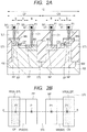
- FIGS. 2A and 2B are a cross section and a plan view illustrating the configuration of a capacitive element in the semiconductor device of the first embodiment.
- FIG. 2A is a cross section, and FIG. 2B is a plan view.
- FIG. 2A corresponds to, for example, the A-A section of FIG. 2B .
- the semiconductor device of the embodiment is formed by using an SOI substrate and has an SOI transistor, a bulk transistor, and a capacitive element.
- the transistor is also called an MISFET (Metal Insulator Semiconductor Field Effect Transistor: MISFET (Metal Insulator Semiconductor Field Effect Transistor: MIS-type field effect transistor) .
- the SOI substrate has a supporting board SB, an insulating layer BX formed over the supporting board SB, and a semiconductor layer SL formed over the insulating layer BX (refer to FIG. 3 ).
- a region in which the SOI transistor is formed is set as a "region 1B”
- a region in which a bulk transistor is formed is set as a "region 1A”
- a region in which a capacitive element is set as a "region 1C”.
- an SOI transistor of the n-channel type and an SOI transistor of the p-channel type are formed.
- the region in which the SOI transistor of the n-channel type is formed is set as "region SN" and the region in which the SOI transistor of the p-channel type is formed is set as "region SP”.
- a bulk transistor of the n-channel type and a bulk transistor of the p-channel type are formed.
- the region in which the bulk transistor of the n-channel type is formed is set as "region BN" and the region in which the bulk transistor of the p-channel type is formed is set as "region BP”.
- n-type capacitive element A capacitive element formed over an n-type well NW is called an n-type capacitive element, and a capacitive element formed over a p-type well is called a p-type capacitive element.
- the region in which the n-type capacitive element is formed is set as "region CN", and the region in which the p-type capacitive element is formed is set as "region CP”.
- the SOI transistor is formed in a so-called SOI region (the region in which the semiconductor layer SL is formed over the supporting board SB via the insulating layer BX), and the bulk transistor is formed in a so-called bulk region (the region from which the insulating layer BX and the semiconductor layer SL are removed, over the supporting board SB).
- SOI region the region in which the semiconductor layer SL is formed over the supporting board SB via the insulating layer BX
- the bulk transistor is formed in a so-called bulk region (the region from which the insulating layer BX and the semiconductor layer SL are removed, over the supporting board SB).
- a region S in the region 1C is the SOI region
- a region B is a bulk region.
- a region X in the region 1C is a region in which the insulating layer BX is formed over the supporting board SB and over which the semiconductor layer SL is removed.
- the regions 1A, 1B, and 1C are also called active regions and defined by element isolation parts (element isolation regions) STI.
- element isolation parts element isolation regions
- each of the regions 1A, 1B, and 1C is surrounded by the element isolation part STI.
- the element isolation part STI is provided in each of the regions. The region is divided into smaller regions.
- the SOI transistor of the n-channel type and the SOI transistor of the p-channel type are formed in the SOI region (the region in which the semiconductor layer SL is formed over the supporting board SB via the insulating layer BX, or the region 1B).
- the supporting board SB is a semiconductor substrate such as a p-type single-crystal silicon substrate.
- the insulating layer BX is, for example, a silicon oxide layer.
- the semiconductor layer SL is, for example, a single-crystal silicon layer.
- the thickness of the insulating layer BX is about a few nm to about 30 nm, and the thickness of the semiconductor layer SL is, for example, a few nm to about 30 nm.
- the SOI transistor of the n-channel type is formed in an active region surrounded (defined) by the element isolation part STI indicated by the region SN.
- the SOI transistor of the n-channel type has a gate electrode GE formed over the semiconductor layer SL via a gate insulating film GI and a source /drain region NS formed in the semiconductor layer SL on both sides of the gate electrodes GE.
- a side-wall film (side-wall spacer) SW are formed on the side wall of the gate electrode GE.
- the source /drain region NS is a source /drain region of an LDD structure and has a low-concentration impurity region EX of the n type formed in a self-aligned manner with respect to the gate electrode GE and a high-concentration impurity region NP of the n type formed in a self-aligned manner with respect to a composite member (composite pattern, composite formation object) of the gate electrode GE and the side-wall film SW.
- the impurity concentration of the high-concentration impurity region NP of the n type is higher than that of the low-concentration impurity region EX of the n type.
- an epitaxial layer is arranged over the semiconductor layer SL on both sides of the gate electrode GE (refer to FIG. 11 ).
- the epitaxial layer EP also contains high-concentration of n-type impurities (such as phosphor (P) and arsenic (As)). Consequently, the high-concentration impurity region NP of the n type is made by the epitaxial layer EP and the semiconductor layer SL.
- the high-concentration impurity region NP of the n type is the impurity region of the n type formed in the stack part of the epitaxial layer EP and the semiconductor layer SL.
- the p-type well PW is formed below the insulating layer BX in the SOI transistor of the n-channel type, that is, in the supporting board SB in the region SN.
- the impurity concentration of the p-type well PW is lower than that of the supporting board SB.
- the SOI transistor of the p-channel type is formed in an active region surrounded (defined) by the element isolation part STI indicated by the region SP.
- the SOI transistor of the p-channel type has the gate electrode GE formed over the semiconductor layer SL via the gate insulating film GI and a source /drain region PS formed in the semiconductor layer SL on both sides of the gate electrodes GE. On the side wall of the gate electrode GE, the side-wall film SW is formed.
- the source /drain region PS is a source /drain region of an LDD structure and has the low-concentration impurity region EX of the p type formed in a self-aligned manner with respect to the gate electrode GE and a high-concentration impurity region PP of the p type formed in a self-aligned manner with respect to a composite member (composite pattern, composite formation object) of the gate electrode GE and the side-wall film SW.
- the impurity concentration of the high-concentration impurity region PP of the p type is higher than that of the low-concentration impurity region EX of the p type.
- the epitaxial layer (EP) is arranged over the semiconductor layer SL on both sides of the gate electrode GE (refer to FIG. 11 ).
- the epitaxial layer EP also contains high-concentration of p-type impurities (such as boron (B)). Consequently, the high-concentration impurity region PP of the p type is made by the epitaxial layer EP and the semiconductor layer SL.
- the high-concentration impurity region PP of the p type is the impurity region of the p type formed in the stack layer part of the epitaxial layer EP and the semiconductor layer SL.
- the n-type well NW is formed below the insulating layer BX in the SOI transistor of the p-channel type, that is, in the supporting board SB in the region SP.
- the gate electrode GE is made by, for example, a polycrystal silicon film, and the gate insulating film GI is made by, for example, a silicon oxide film.
- a metal silicide film MS as a reaction layer (compound layer) of metal and semiconductor is formed.
- An interlayer insulating film IL1 is formed over the gate electrode GE, the source /drain regions (NS and PS) and the like. Over the source /drain regions (NS and PS), a plug (coupling part) P1 is formed via the metal silicide film MS. The plug P1 is made by a conductive film buried in a connection hole C1 provided in the interlayer insulating film IL1. Over the plug P1, a wire M1 is formed. Although not illustrated in the section of FIG. 1 , the plug P1 and the wire M1 above it are formed also over the gate electrode GE, the n-type well NW, and the p-type well PW.
- threshold voltage By applying a potential to the well below the insulating layer BX in the SOI transistor via the plug p1, threshold voltage can be adjusted.
- the bulk transistor of the n-channel type and the bulk transistor of the p-channel type are formed in the bulk regions (the region from which the insulating layer BX and the semiconductor layer SL are removed, the region BN, and the region BN over the supporting board SB).
- the bulk transistor of the n channel type is formed in an active region surrounded (defined) by the element isolation part STI indicated by the region BN.
- the bulk transistor of the n-channel type has the gate electrode GE formed over the p-type well PW in the supporting board SB via the gate insulating film GI and source /drain regions NB formed in the supporting board (p-type well PW) SB on both sides of the gate electrodes GE.
- the side-wall film SW is formed on the side wall of the gate electrode GE.
- the source /drain region NS is a source /drain region of an LDD structure and has the low-concentration impurity region EX of the n type formed in a self-aligned manner with respect to the gate electrode GE and the high-concentration impurity region NP of the n type formed in a self-aligned manner with respect to a composite member of the gate electrode GE and the side-wall film SW.
- the impurity concentration of the high-concentration impurity region NP of the n type is higher than that of the low-concentration impurity region EX of the n type.
- the bulk transistor of the p channel type is formed in an active region surrounded (defined) by the element isolation part STI indicated by the region BP.
- the bulk transistor of the p-channel type has the gate electrode GE formed over the n-type well NW in the supporting board SB via the gate insulating film GI and source /drain regions PB formed in the supporting board (n-type well NW) SB on both sides of the gate electrodes GE.
- the side-wall film SW is formed on the side wall of the gate electrode GE.
- the source /drain region PB is a source /drain region of an LDD structure and has the low-concentration impurity region EX of the p type formed in a self-aligned manner with respect to the gate electrode GE and the high-concentration impurity region PP of the p type formed in a self-aligned manner with respect to a composite member of the gate electrode GE and the side-wall film SW.
- the impurity concentration of the high-concentration impurity region PP of the p type is higher than that of the low-concentration impurity region EX of the p type.
- the gate electrode GE is made by, for example, a polycrystal silicon film, and the gate insulating film GI is made by, for example, a silicon oxide film.
- the metal silicide film MS as a reaction layer (compound layer) of metal and semiconductor is formed.
- the interlayer insulating film IL1 is formed over the gate electrode GE, the source /drain regions (NS and PS) and the like. Over the source /drain regions (NB and PB), the plug P1 is formed via the metal silicide film MS. The plug P1 is made by a conductive film buried in the coupling hole C1 provided in the interlayer insulating film IL1. Over the plug P1, the wire M1 is formed. Although not illustrated in the section of FIG. 1 , the plug P1 and the wire M1 above it are formed also over the gate electrode GE.
- the region 1C Two capacitive elements (an n-type capacitive element and a p-type capacitive element) are formed in the region 1C.
- the SOI region and the bulk region mixedly exist in the region 1C.
- the region S in the region 1C is an SOI region
- the region B is a bulk region.
- the region X in the region 1C is a region in which the insulating layer BX is formed over the supporting board SB but the semiconductor layer SL over the insulating layer BX is removed.
- the capacitive element (n-type capacitive element) is formed in the active region surrounded (defined) by the element isolation part STI indicated by the region CN.
- the capacitive element (n-type capacitive element) has the supporting board SB, the insulating layer BX formed over the supporting board SB, and the semiconductor layer SL formed over the insulating layer BX.
- the n-type well NW is formed in the supporting board SB in the region CN.
- the epitaxial layer (EP) is arranged over the semiconductor layer SL (refer to FIG. 11 ).
- n-type impurities such as phosphor P or arsenic (As)
- the high-concentration impurity region NP of the n type is obtained.
- an opening is provided in the insulating layer BX.
- the supporting board (n-type well NW) SB exposed from the opening the high-concentration impurity region NP of the n type is formed.
- the capacitive element has, in the region 1C (CN), a top electrode made by the layer stack part (the high-concentration impurity region NP of the n type) of the semiconductor layer SL and the epitaxial layer (EP), a capacitance insulating film made by the insulating layer BX, and a bottom electrode made by the supporting board (n-type well NW) SB.
- the high-concentration impurity region NP of the n type in the supporting board (n-type well NW) SB becomes a lead part of the bottom electrode.
- the metal silicide layer MS is formed.
- the interlayer insulating film 1L1 is formed over the top electrode (the layer stack part (the high-concentration impurity region NP of the n type) of the semiconductor layer SL and the epitaxial layer (EP)), the capacitance insulating film (the insulating layer BX), and the lead part (the high-concentration impurity region NP of the n type in the supporting board (n-type well NW)) SB of the bottom electrode.
- the plugs P1 are formed via the metal silicide film MS over the top electrode (the layer stack part (the high-concentration impurity region NP of the n type) of the semiconductor layer SL and the epitaxial layer (EP)) and the lead part (the high-concentration impurity region NP of the n type in the supporting board (n-type well NW) SB) of the bottom electrode.
- the plug P1 is made by the conductive film buried in the coupling hole C1 provided in the interlayer insulating film IL1. As illustrated in FIG. 2A , the n-type capacitive element (CN) is coupled between the wires M1 (between the nodes n3 and n4).
- the capacitive element (p-type capacitive element) is formed in the active region surrounded (defined) by the element isolation part STI indicated by the region CP.
- the capacitive element has the supporting board SB, the insulating layer BX formed over the supporting board SB, and the semiconductor layer SL formed over the insulating layer BX.
- the p-type well PW is formed in the supporting board SB in the region CP.
- EP is arranged (refer to FIG. 11 ).
- p-type impurities such as boron B
- the high-concentration impurity region PP of the p type is obtained.
- an opening is provided in the insulating layer BX.
- the high-concentration impurity region PP of the p type is formed in the active region surrounded (defined) by the element isolation part STI indicated by the region CP.
- the capacitive element has the supporting board SB, the insulating layer BX formed over the supporting board SB, and the semiconductor layer SL formed over the insulating layer
- the capacitive element has, in the region 1C (CP), a top electrode made by the layer stack part (the high-concentration impurity region PP of the p type) of the semiconductor layer SL and the epitaxial layer (EP), a capacitance insulating film made by the insulating layer BX, and a bottom electrode made by the supporting board (p-type well PW) SB.
- the high-concentration impurity region PP of the p type in the supporting board (p-type well PW) SB becomes a lead part of the bottom electrode.
- the metal silicide layer MS is formed in the layer stack part (the high-concentration impurity region PP of the p type) of the semiconductor layer SL and the epitaxial layer (EP) and the upper part (surface layer part) of the high-concentration impurity region PP of the p type in the supporting board (p-type well PW) SB.
- the interlayer insulating film 1L1 is formed over the top electrode (the layer stack part (the high-concentration impurity region PP of the p type) of the semiconductor layer SL and the epitaxial layer (EP)), the capacitance insulating film (the insulating layer BX), and the lead part (the high-concentration impurity region PP of the p type in the supporting board (p-type well PW)) SB of the bottom electrode.
- the plugs P1 are formed via the metal silicide film MS over the top electrode (the layer stack part (the high-concentration impurity region PP of the p type) of the semiconductor layer SL and the epitaxial layer (EP)) and the lead part (the high-concentration impurity region PP of the p type in the supporting board (p-type well PW) SB) of the bottom electrode.
- the plug P1 is made by the conductive film buried in the coupling hole C1 provided in the interlayer insulating film IL1. As illustrated in FIG. 2A , the p-type capacitive element (CP) is coupled between the wires M1 (between the nodes n1 and n2).
- the capacitance per unit area can be increased.
- the SOI transistor is formed in the main surface of so-called SOTB (Silicon On Thin Buried oxide) of the semiconductor layer SL over the insulating layer BX as a thin film.
- SOTB Silicon On Thin Buried oxide
- the threshold voltage can be adjusted.
- the thickness of the insulating layer BX of the thin film is 50 nm or less and, more preferably, a few nm to 30 nm. Consequently, the insulating layer BX sufficiently functions as a capacitance insulating film and can be used as a capacitive element of high capacitance.
- the capacitance of the capacitive element can be adjusted by, for example, an overlap region of the top and bottom electrodes, that is, an overlap region of the stack layer part of the semiconductor layer SL and the epitaxial layer (EP) and the supporting board (the well PW or NW).
- the overlap region is indicated by dot-hatching (gray) in FIG. 2B .
- the thickness of the insulating layer BX is set to about 20 nm, to assure the capacitance of 10 pF, it is sufficient to set the overlap region to about 5647 ⁇ m 2 .
- To assure the capacitance of 5 pF it is sufficient to set the overlap region to about 2823 ⁇ m 2 . In such a manner, a capacitive element (fixed capacitance) of high capacitance can be realized using a small area.
- the manufacture process of the SOI transistor can be shared.
- the supporting board (the n-type well NW or p-type well PW) SB as the bottom electrode, the manufacture process of the SOI transistor can be shared.
- the high-concentration impurity region NP of the n type or the high-concentration impurity region PP of the p type in the supporting board SB exposed from the opening in the insulating layer BX as the lead part of the bottom electrode the manufacture process of the bulk transistor can be shared. The sharing of the manufacture processes will become the column of "description of manufacturing method" which will be described later.
- an interlayer insulating film IL2, a wire M2, and the like are formed over the wire M1.
- plugs are formed also in the interlayer insulating film IL2.
- an interlayer insulating film IL3, a wire M3, and the like are formed over the wire M2, over the wire M2, an interlayer insulating film IL3, a wire M3, and the like are formed.
- an interlayer insulating film IL4, a wire M4, and the like are formed.
- an interlayer insulating film IL5, a wire M5, and the like are formed.
- a stack-layer film of an insulating film PSN and a protection film RF is formed. A part of the wire M5 is exposed from an opening in the stack-layer film. The exposed part of the wire M5 becomes a pad electrode (external coupling terminal) PE.
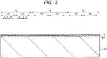
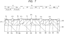
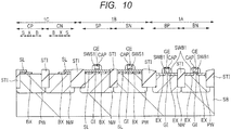
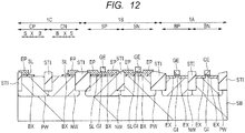
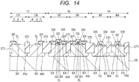
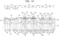
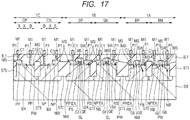
- FIGS. 3 to 17 are cross sections illustrating a process of manufacturing the semiconductor device of the embodiment.
- an SOI substrate (semiconductor wafer) is prepared as a substrate.
- the SOI substrate has the supporting board SB, the insulating layer BX formed over the supporting board SB, and the semiconductor layer SL formed over the insulating layer BX.
- the supporting board SB is a semiconductor substrate made of, for example, p-type single-crystal silicon (Si), and the insulating layer BX is, for example, a layer made of silicon oxide.
- the semiconductor layer SL is, for example, a layer made of single-crystal silicon having resistance of about 1 to 10 Qcm.
- the thickness of the insulating layer BX is about a few nm to about 30 nm.
- the thickness of the semiconductor layer SL is, for example, a few nm to about 30 nm.
- the element isolation part STI is formed.
- a hard mask (not illustrated) made by a silicon nitride film or the like is formed in a region left as an active region, and dry etching is performed by using the hard mask as a mask, thereby eliminating a part of the semiconductor layer SL, the insulating layer BX, and the supporting board SB to form an element isolation trench.
- Etching of a film in a lower layer using a film of a desired shape as a mask is called patterning.
- the element isolation trench penetrates the semiconductor layer SL and the insulating layer BX and reaches some midpoint in the supporting board SB. In other words, the bottom of the element isolation trench is positioned deeper than the bottom face (bottom part) of the insulating layer BX.
- an insulating film is formed with a film thickness to a degree that the element isolation trench is buried.
- a silicon oxide film is deposited as an insulating film by using the CVD (Chemical Vapor Deposition) method or the like.
- the insulating film which is not in the element isolation trench is removed by using the CMP (Chemical Mechanical Polishing), etch back method, or the like until the hard mask is exposed.
- the element isolation part STI in which the insulating film is buried in the element isolation trench can be formed.
- the element isolation part STI is formed to prevent interferences among elements formed in the regions 1A, 1B, and 1C. Subsequently, the hard mask is removed.
- the p-type wells PW in the regions are formed.
- a photoresist film (not illustrated) in which a formation region of the p-type well PW is opened as a mask, the impurity of the p type is ion-implanted into the supporting board SB below the insulating layer BX. Subsequently, the photoresist film is removed by ashing process of the like.
- the p-type wells PW in the regions may be formed one by one while varying the ion implantation condition.
- the n-type wells NW are formed.
- a photoresist film (not illustrated) in which a formation region of the n-type well NW in each region is opened as a mask, the impurity of the p type is ion-implanted into the supporting board SB below the insulating layer BX. Subsequently, the photoresist film is removed by ashing process of the like.
- the p-type wells PW in the regions may be formed one by one while varying the ion implantation condition.
- the semiconductor layer SL in the region 1A and parts (regions X and B) in the region 1C is removed.
- the semiconductor layer SL in parts in the regions 1A and 1C is etched.
- the photoresist film is removed by ashing process or the like.
- the insulating layer BX in the region 1A and a part (region B) in the region 1C is removed.
- the photoresist film (not illustrated) in which the region of removing the insulating layer BX is open as a mask
- the insulating layer BX in the region 1A and a part (region B) in the region 1C is etched. After that, the photoresist film is removed by ashing process or the like.
- the gate insulating film GI and the gate electrode GE are formed in the regions.
- the gate insulating film GI made by the silicon oxide film is formed.
- a conductive film which becomes a gate electrode is formed.
- a polycrystal silicon film is formed by using the CVD method or the like.
- a cap insulating film CAP is formed.
- a silicon nitride film is formed as the cap insulating film CAP by using the CVD method or the like.
- the source /drain regions in the SOI transistor and the bulk transistor, the high-concentration impurity region NP of the n type or the high-concentration impurity region PP of the p type in the layer stack part of the semiconductor layer SL and the epitaxial layer EP, the high-concentration impurity region NP in the n-type well NW, and the high-concentration impurity region PP of the p type in the p-type well PW are formed.
- the low-concentration impurity region EX of the n type and the low-concentration impurity region EX of the p type are formed in the supporting board (n-type well NW and p-type well PW) SB on both sides of the gate electrode GE.
- the photoresist film (not illustrated) having an opening in the region BN in the region 1A as a mask, n-type impurities are introduced to both sides of the gate electrode GE by the ion implantation method.
- the photoresist film (not illustrated) is removed by ashing process or the like.
- a photoresist film (not illustrated) having an opening in the region BP in the region 1A as a mask, p-type impurities are introduced to the n-type wells NW on both sides of the gate electrode GE by the ion implantation method.
- the photoresist film (not illustrated) is removed by ashing process or the like.
- side-wall films (SWS1 and SWB1) made by an insulating film are formed on the side walls of the gate electrode GE.
- the insulating film is formed in the regions 1A and 1B and is subjected to anisotropic etching, thereby making the side-wall films (SWS1 and SWB1) remain.
- the side-wall film may remain on the side walls of the semiconductor layer SL in the region 1C.
- the region 1B and the regions B in the region 1C are covered with a mask film to form the epitaxial layer EP over the semiconductor layer SL in the regions 1B and 1C.
- a mask film to form the epitaxial layer EP over the semiconductor layer SL in the regions 1B and 1C.
- a silicon layer is formed as the epitaxial layer EP over the semiconductor layer SL.
- the side-wall films (SWS1 and SWB1) in the side walls of the gate electrodes GE in the regions are removed and, further, the cap insulating film CAP is removed.
- the low-concentration impurity region EX of the n type and the low-concentration impurity region EX of the p type are formed in the layer stack part of the semiconductor layer SL and the epitaxial layer EP on both sides of the gate electrode GE.
- n-type impurities are introduced into the semiconductor layer SL on both sides of the gate electrode GE by using a photoresist film (not illustrated) having an opening in the region SN in the region 1B as a mask by the ion implantation method.
- the photoresist film (not illustrated) is removed by ashing process or the like.
- p-type impurities are introduced into the semiconductor layer SL on both sides of the gate electrode GE by using a photoresist film (not illustrated) having an opening in the region SP in the region 1B as a mask by the ion implantation method.
- the photoresist film (not illustrated) is removed by ashing process or the like.
- the side-wall film SW made by an insulating film is formed on the side walls of the gate electrode GE in each region.
- the insulating film is formed in the regions 1A and 1B and is subjected to anisotropic etching to make the side-wall film SW remain.
- the side-wall film may remain on the side walls of the layer stack part of the semiconductor layer SL and the epitaxial layer EP in the region 1C.
- the high-concentration impurity region NP of the n type and the high-concentration impurity region PP of the p type are formed in each of the regions.
- n-type impurities are introduced by the ion implantation method using a photoresist film (not illustrated) having openings in the region BN in the region 1A, the region SN in the region 1B, and the region CN in the region 1C as a mask by the ion implantation method.
- the photoresist film (not illustrated) is removed by ashing process or the like.
- p-type impurities are introduced by the ion implantation method using a photoresist film (not illustrated) having openings in the region BP in the region 1A, the region SP in the region 1B, and the region CP in the region 1C as a mask by the ion implantation method.
- the photoresist film (not illustrated) is removed by ashing process or the like.
- the RTA Rapid Thermal Anneal
- a source /drain region NS of an SOI transistor of the n channel type made by the low-concentration impurity region EX of the n type and the high-concentration impurity region NP of the n type is formed.
- a source /drain region NB of a bulk transistor of the n channel type made by the low-concentration impurity region EX of the n type and the high-concentration impurity region NP of the n type is formed.
- the high-concentration impurity region NP of the n type which becomes the lead part of the bottom electrode (n-type well NW) is formed.
- the regions may be formed one by one while varying the ion implantation condition of the high-concentration impurity region NP of the n type in the regions.
- a source /drain region PS of an SOI transistor of the p channel type made by the low-concentration impurity region EX of the p type and the high-concentration impurity region PP of the p type is formed.
- a source /drain region PB of a bulk transistor of the p channel type made by the low-concentration impurity region EX of the p type and the high-concentration impurity region PP of the p type is formed.
- the high-concentration impurity region PP of the p type which becomes the lead part of the bottom electrode (p-type well PW) is formed.
- the regions may be formed one by one while varying the ion implantation condition of the high-concentration impurity region PP of the p type in the regions.
- the metal silicide film MS is formed by the salicide (Self Aligned Silicide) technique.
- a nickel silicide film is formed.
- a metal film such as a nickel (Ni) film is formed in the regions 1A, 1B, and 1C and is subjected to thermal process.
- silicidation reaction is caused in a contact region of the gate electrode GE, the high-concentration impurity region NP of the n type, the high-concentration impurity region PP of the p type, and the Ni film. After that, by removing the Ni film which is unreacted, a nickel silicide film is formed.
- the interlayer insulating film IL1, the plug P1, and the wire M1 are formed in each of the regions.
- a layer stack film of a thin silicon nitride film (not illustrated) and a silicon oxide film is formed as the interlayer insulating film IL1 by the CVD method or the like.
- the coupling holes C1 are formed.
- a layer stack film of a barrier film (not illustrated) and a metal film (for example, a tungsten film) is deposited as a conductive film.
- the deposited conductive film other than the conductive film in the coupling holes C1 is removed by using the CMP method or the like.
- the plugs P1 are formed.
- the wires M1 are formed over the interlayer insulating film IL1 including the top of the plugs P1.
- a conductive film such as an Al film is deposited over the interlayer insulating film IL1 including the plugs P1 and patterned, thereby forming the wires M1.
- the wires M1 may be formed by the damascene method. For example, by forming an insulating film over the interlayer insulating film IL1 and patterning it, a wire trench is formed. After that, by burying the wire trench with a conductive film such as a copper film, the wire M1 is formed.
- the interlayer insulating films (IL2 to IL5), the plugs (P2 to P5), and the wires (M2 to M5) above the wire M1 are formed.
- the interlayer insulating films (IL2 to IL5), the plugs (P2 to P5), and the wires (M2 to M5) above the wire M1 are formed.
- the wire M5 as the highest-layer wire the insulating film PSN made by a silicon nitride film or the like is formed and patterned, thereby exposing a part of the highest-layer wire M5.
- the exposed part becomes the pad electrode PE.
- the protection film RF made of photosensitive polyimide is formed over the insulating film PSN, and the protection film RF over the pad electrode PE is removed (refer to FIG. 1 ).
- the semiconductor device of the embodiment can be formed.
- the configuration part of the capacitive element and the configuration part of the SOI transistor and the bulk transistor can be simultaneously formed. Consequently, a capacitive element of high capacitance can be formed with an SOI transistor and a bulk transistor in a short process.
- a formation region (region S) of the insulating layer BX constructing a capacitance insulating film of a capacitive element is defined by the element isolation part STI.
- a deep n-type well DNW is formed below the p-type well PW.
- the p-type well PW as a component of the bottom electrode of the capacitive element can be electrically isolated from the p-type supporting board SB. Therefore, for example, the potential of the p-type well PW as a component of the bottom electrode can be set to a potential other than the substrate potential (for example, ground potential).
- the deep n-type well DNW may be formed below the p-type well PW.
- the potential of the p-type well PW below each transistor can be set to a potential other than the substrate potential (for example, ground potential).
- FIG. 18 is a cross section illustrating the configuration of the semiconductor device of the embodiment.
- FIGS. 19A and 19B are a cross section and a plan view illustrating the configuration of a capacitive element in the semiconductor device of the embodiment.
- FIG. 19A is a cross section, and
- FIG. 19B is a plan view.
- FIG. 19A corresponds to the A-A section in FIG. 19B .
- the semiconductor device of the second embodiment is formed by using an SOI substrate and has an SOI transistor, a bulk transistor, and a capacitive element.
- the configuration of an SOI transistor of an n-channel type and that of an SOI transistor of a p-channel type is similar to that of the case of the first embodiment (refer to FIGS. 18 and 1 ).
- the p-type well PW is formed below the insulating layer BX of the SOI transistor of the n channel type, that is, in the supporting board SB in the region SN.
- the impurity concentration of the p-type well PW is higher than that of the supporting board SB.
- the deep n-type well DNW is formed below the p-type well PW. That is, the side faces and the bottom face of the p-type well PW are covered with the element isolation parts STI and the deep n-type well DNW.
- the configuration of the bulk transistor of the n-channel type and the bulk transistor of the p-channel type is similar to that in the case of the first embodiment (refer to FIGS. 18 and 1 ).
- the deep n-type well DNW is formed below the p-type well PW in the region BN in which the bulk transistor of the n-channel type is formed. That is, the side faces and the bottom face of the p-type well PW are covered with the element isolation parts STI and the deep n-type well DNW.
- the configuration of two capacitive elements (an n-type capacitive element and a p-type capacitive element) formed in the region 1C is similar to that in the case of the first embodiment (refer to FIGS. 18 and 1 ) except for the point that the insulating layer BX is defined by the element isolation part STI and the point that the deep n-type well DNW is formed.
- the capacitive element (n-type capacitive element) is formed in the region CN.
- the capacitive element has the supporting board SB, the insulating layer BX formed over the supporting board SB, and the semiconductor layer SL formed over the insulating layer BX.
- the n-type well NW is formed in the supporting board SB in the region CN.
- the insulating layer BX is formed in an active region surrounded (defined) by the element isolation parts STI (refer to FIG. 19B ).
- a lead part of a bottom electrode made by the high-concentration impurity region NP of the n type is formed in the active region surrounded (defined) by the element isolation parts STI (refer to FIG. 19B ).
- the bottom of the insulating layer BX and the lead part (high-concentration impurity region NP of the n type) of the bottom electrode are electrically coupled via the n-type well NW below the element isolation parts STI.
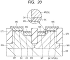
- an overhang part OH occurs at an end part of the insulating layer BX depending on processing (etching) precision of the semiconductor layer SL and the insulating layer BX.
- the characteristic of the capacitive element is fluctuated and it becomes difficult to adjust the capacitance.
- FIG. 20 is a cross section illustrating the configuration of a semiconductor device of a comparative example of the second embodiment.
- the capacitive element (p-type capacitive element) is formed in the region CP.
- a capacitive element (p-type capacitive element) has the supporting board SB, the insulating layer BX formed over the supporting board SB, and the semiconductor layer SL formed over the insulating layer BX.
- the p-type well PW is formed in the supporting board SB in the region CP.
- the insulting layer BX is formed in the active region surrounded (defined) by the element isolation part STI (refer to FIG. 19B ).
- the lead part of the bottom electrode made by the high-concentration impurity region PP of the p type is formed in the active region surrounded (defined) by the element isolation part STI (refer to FIG. 19B ).
- the bottom of the insulating layer BX and the lead part (high-concentration impurity region PP of the p type) of the bottom electrode are electrically coupled via the p-type well PW below the element isolation parts STI.
- the region CP by defining the formation region of the insulating layer BX by the element isolation parts STI, in a manner similar to the case of the n-type capacitive element, variations in the formation region of the insulating layer BX which becomes a capacitance insulating film, variations in the film thickness, and the like can be suppressed.
- the deep n-type well DNW is formed below the p-type well PW in the region CP in which the p-type capacitive element is formed. That is, the side faces and the bottom face of the p-type well PW are covered with the element isolation parts STI and the deep n-type well DNW.
- the potential of the p-type well PW as a component of the bottom electrode can be set to a potential other than the substrate potential (for example, ground potential).
- the configurations of the interlayer insulating film (IL1 to IL5), the plugs (P1 and the like), and the wire (M1 to M5) are similar to those in the case of the first embodiment.
- the configurations of the insulating film PSN, the protection film RF, and the pad electrode PE are also similar to those in the case of the first embodiment.
- the processes of the semiconductor device of the second embodiment are similar to those in the case of the first embodiment except for the process of forming the element isolation part STI and the process of forming the deep n-type well DNW.
- the element isolation part STI in the SOI substrate, it is sufficient to form the element isolation part STI so as to surround the formation region of the insulating layer BX in the region CP (refer to FIGS. 4 and 18 ).
- the deep n-type well DNW in addition to the p-type well and the n-type well NW.
- a photoresist film (not illustrated) in which a formation region of the deep n-type well DNW is opened as a mask, n-type impurities are ion-implanted into a deep position in the supporting board SB below the insulating layer BX. Subsequently, the photoresist film is removed by ashing process of the like.
- the order of forming the above-described wells is not limited, for example, the deep n-type well DNW is formed, the p-type well is formed (refer to FIG. 5 ) and, further, the n-type well NW is formed (refer to FIG. 6 ).
- a varactor in addition to an SOI transistor, a bulk transistor, and a capacitive element (n-type capacitive element and a p-type capacitive element), a varactor (MOS varactor, also called an MOS-type variable capacitive element) is provided.
- MOS varactor also called an MOS-type variable capacitive element
- FIG. 21 is a cross section illustrating the configuration of the semiconductor device of the third embodiment.
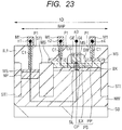
- FIGS. 22 and 23 are cross sections each illustrating the configuration of a capacitive element in the semiconductor device of the third embodiment.
- the semiconductor device of the third embodiment is formed by using an SOI substrate and has an SOI transistor, a bulk transistor, a varactor, and a capacitive element.
- a region in which the SOI transistor is formed is set as "region 1B”
- the region in which the varactor transistor is formed is set as "region 1C”
- the region in which the varactor is formed is set as "region 1D”.
- the "region 1B" as the region in which the SOI transistor is formed is omitted.
- an SOI transistor of the n channel type and an SOI transistor of the p channel type are formed (refer to FIG. 1 ).
- a bulk transistor of the n channel type and a bulk transistor of the p channel type are formed.
- two capacitive elements (an n-type capacitive element and a p-type capacitive element) are formed.
- the p-type capacitive element formed in the region CP is omitted.
- the varactor formed in the region 1D Since the configurations of the SOI transistor, the bulk transistor, and the capacitive elements (the n-type capacitive element and the p-type capacitive element) are similar to those in the cases of the first and second embodiments, hereinafter, the varactor formed in the region 1D will be described.
- an n-type varactor and a p-type varactor are formed in the region 1D.
- the n-type varactor and the p-type varactor have configurations similar to those of the SOI transistor of the n-channel type and the SOI transistor of the p-channel type, respectively, and can be formed by similar processes.
- the n-type varactor ( FIG. 21 ) is formed in an active region surrounded (defined) by the element isolation parts STI indicated by a region BAN.
- the n-type varactor has the gate electrode GE formed over the semiconductor layer SL via the gate insulating film GI and the source /drain region NS formed in the semiconductor layer SL on both sides of the gate electrode GE. On the side walls of the gate electrode GE, the side-wall film SW is formed.
- the source /drain region NS is a source /drain region of the LDD structure, and has the low-concentration impurity region EX of the n type formed in a self-aligned manner with respect to the gate electrode GE, and the high-concentration impurity region NP of the n type formed in a self-aligned manner with respect to the composite member of the gate electrode GE and the side-wall film SW.
- the impurity concentration of the high-concentration impurity region NP of the n type is higher than that of the low-concentration impurity region EX of the n type.
- the epitaxial layer (EP) is arranged over the semiconductor layer SL on both sides of the gate electrode GE, and the high-concentration impurity region NP of the n type is formed in the layer stack part.
- the p-type well PW is formed below the insulating layer BX of the n-type varactor, that is, in the supporting board SB in the region BAN.
- the impurity concentration of the p-type well PW is higher than that of the supporting board SB.
- the high-concentration impurity region PP of the p type is formed in the p-type well.
- the high-concentration impurity region PP of the p type is formed in a bulk region (the region from which the insulating layer BX and the semiconductor layer SL over the supporting board SB are removed) in the region BAN.
- the deep n-type well DNW is formed below the p-type well PW. That is, the side faces and the bottom face of the p-type well PW are covered with the element isolation parts STI and the deep n-type well DNW.
- the plug P1 is formed via the metal silicide film MS.
- n-type varactor that is, the potential difference is given between the nodes n4 and n2 and potential is applied to the node n3 to make the potential of the node n3 and that of the node n1 the same
- a MOS capacitor CG obtained by the oxide film of the gate and the capacitor CN obtained by the insulating layer BX are coupled in parallel between the node n2 (n4) and the node n3 (n1).
- the p-type varactor ( FIG. 21 ) is formed in the active region surrounded (defined) by the element isolation part STI indicated by a region BAP.
- the p-type varactor has the gate electrode GE formed over the semiconductor layer SL via the gate insulating film GI and the source /drain region PS formed in the semiconductor layer SL on both sides of the gate electrode GE. On the side walls of the gate electrode GE, the side-wall film SW is formed.
- the source /drain region PS is a source /drain region of the LDD structure, and has the low-concentration impurity region EX of the p type formed in a self-aligned manner with respect to the gate electrode GE, and the high-concentration impurity region PP of the p type formed in a self-aligned manner with respect to the composite member of the gate electrode GE and the side-wall film SW.
- the impurity concentration of the high-concentration impurity region PP of the p type is higher than that of the low-concentration impurity region EX of the p type.
- the epitaxial layer (EP) is arranged over the semiconductor layer SL on both sides of the gate electrode GE, and the high-concentration impurity region PP of the p type is formed in the layer stack part.
- the n-type well NW is formed below the insulating layer BX of the p-type varactor, that is, in the supporting board SB in the region BAP.
- the high-concentration impurity region of the n type is formed in the n-type well NW.
- the high-concentration impurity region NP of the n type is formed in a bulk region (the region from which the insulating layer BX and the semiconductor layer SL over the supporting board SB are removed) in the region BAP.
- the gate electrode GE is made by, for example, a polycrystal silicon film, and the gate insulating film GI is made by, for example, a silicon oxide film.
- the metal silicide film MS as a reaction layer (compound layer) of metal and semiconductor is formed.
- the interlayer insulating film IL1 is formed over the gate electrode GE, the source /drain regions (NS and PS) and the like. Over the source /drain regions (NS and PS), the plug (coupling part) P1 is formed via the metal silicide film MS. The plug P1 is made by a conductive film buried in the connection hole C1 provided in the interlayer insulating film IL1. Over the plug P1, the wire M1 is formed.
- the plug P1 is formed via the metal silicide film MS.
- the MOS capacitor CG obtained by the oxide film of the gate and the capacitor CP obtained by the insulating layer BX are coupled in parallel between the node n2 (n4) and the node n3 (n1).
- the potential of the p-type well PW can be set to a potential other than the substrate potential (for example, the ground potential. That is, as described above, the potential of the node n3 and that of the node n1 can be made the same.
- FIGS. 24A and 24B are circuit diagrams illustrating a PLL circuit and a low-pass filter in application example 1.
- FIG. 24A illustrates a PLL circuit
- FIG. 24B illustrates a low-pass filter.
- the PLL circuit has, for example, a reference oscillator 10, a fixed frequency divider (1/M) 20, a phase comparator (PC) 30, a low-pass filter (LPF) 40, a voltage-controlled oscillator (VOC) 50, and a variable frequency divider (1/N) 60.
- the PLL circuit is a feedback circuit for adjusting oscillation frequency fo of the voltage-controlled oscillator 50 to desired frequency f R .
- the high output frequency is supplied to the phase comparator 30 via the variable frequency divider 60 and converted to a voltage signal corresponding to high output frequency in the low-pass filter 40, and the voltage signal is output.
- the low-pass filter 40 has a resistor R coupled between an input potential Vin and an output potential Vout and a capacitor C coupled between the output potential Vout and a reference potential.
- the capacitive element n-type capacitive element, p-type capacitive element
- the varactor descried in the first to third embodiments
- a capacitor of high capacitance can be realized with small area, and is suitably used as the low-pass filter.
- the p-type well PW is electrically isolated from the n-type supporting board SB by the deep n-type well DNW. Consequently, the device is not easily influenced by signal noise caused by operation of another circuit, and the operation characteristics become excellent.
- the device is suitably used for a circuit for high-speed data transfer of multiple channels, the PLL circuit described in the application example 1, an AD converter, and the like.
- the n-type varactor and the p-type varactor described in the third embodiment may be coupled in parallel and used as a capacitor.
- the n-type varactor and the p-type varactor operate in a complemental manner in correspondence to fluctuations in potential, and stability of the capacitor can be improved.
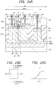
- FIGS. 25A, 25B, and 25C are a cross section, a circuit diagram, and a capacitance change graph illustrating an n-type varactor unit of the application example 3.
- FIG. 25A is the cross section
- FIG. 25B is the circuit diagram
- FIG. 25C is the capacitance change graph.
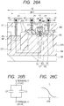
- FIGS. 26A, 26B, and 26C are a cross section, a circuit diagram, and a capacitance change graph illustrating a p-type varactor unit of the application example 3.
- FIG. 26A is the cross section
- FIG. 26B is the circuit diagram
- FIG. 26C is the capacitance change graph.
- FIGS. 27A and 27B are a circuit diagram and a capacitance change graph illustrating a capacitive element of the application example 3.
- FIG. 27A is the circuit diagram
- FIG. 27B is the capacitance change graph.
- FIGS. 25A and 25B The configuration of the n-type varactor and the p-type varactor illustrated in FIGS. 25A and 25B is as described in the third embodiment.
- a MOS capacitor CG obtained by the oxide film of the gate and the capacitor CN obtained by the insulating layer BX are coupled in parallel between the terminal 1 (n3, n1) and the terminal 2 (n2, n4).
- the capacitance C vertical axis
- the MOS capacitor CG obtained by the oxide film of the gate and the capacitor CP obtained by the insulating layer BX are coupled in parallel between the terminal 3 (n3, n1) and the terminal 4 (n2, n4).
- the capacitance C vertical axis
- V34 potential between the terminals 3 and 4 (horizontal axis) becomes higher.
- the MOS capacitor CG obtained by the oxide film of the gate and the capacitor CN obtained by the insulating layer BX in the n-type varactor and the MOS capacitor CG obtained by the oxide film of the gate and the capacitor CP obtained by the insulating layer BX in the p-type varactor are coupled in parallel.
- the coupling part of the terminals 1 and 3 is set as the terminal AP and the coupling part of the terminals 2 and 4 is set as the terminal BP
- the composite capacitance becomes almost constant regardless of changes in the potential VAB (horizontal axis) between the terminals AP and BP.
Landscapes
- Metal-Oxide And Bipolar Metal-Oxide Semiconductor Integrated Circuits (AREA)
- Semiconductor Integrated Circuits (AREA)
- Thin Film Transistor (AREA)
- Engineering & Computer Science (AREA)
- Power Engineering (AREA)
- Physics & Mathematics (AREA)
- Geometry (AREA)
Applications Claiming Priority (1)
| Application Number | Priority Date | Filing Date | Title |
|---|---|---|---|
| JP2016251302A JP2018107253A (ja) | 2016-12-26 | 2016-12-26 | 半導体装置および半導体装置の製造方法 |
Publications (2)
| Publication Number | Publication Date |
|---|---|
| EP3340299A2 true EP3340299A2 (de) | 2018-06-27 |
| EP3340299A3 EP3340299A3 (de) | 2018-10-31 |
Family
ID=60190672
Family Applications (1)
| Application Number | Title | Priority Date | Filing Date |
|---|---|---|---|
| EP17198689.6A Withdrawn EP3340299A3 (de) | 2016-12-26 | 2017-10-26 | Halbleiterbauelement und verfahren zur herstellung eines halbleiterbauelements |
Country Status (6)
| Country | Link |
|---|---|
| US (1) | US10446543B2 (de) |
| EP (1) | EP3340299A3 (de) |
| JP (1) | JP2018107253A (de) |
| KR (1) | KR20180075404A (de) |
| CN (1) | CN108242443B (de) |
| TW (1) | TW201838093A (de) |
Families Citing this family (4)
| Publication number | Priority date | Publication date | Assignee | Title |
|---|---|---|---|---|
| CN113241345B (zh) * | 2021-07-12 | 2021-11-26 | 广州粤芯半导体技术有限公司 | 半导体器件结构及其形成方法 |
| JP7728198B2 (ja) * | 2022-02-14 | 2025-08-22 | セイコーNpc株式会社 | 可変容量素子ユニット及びその製造方法 |
| FR3139234A1 (fr) * | 2022-08-31 | 2024-03-01 | Stmicroelectronics Sa | Protection contre des décharges électrostatiques |
| US20250338603A1 (en) * | 2024-04-29 | 2025-10-30 | Globalfoundries U.S. Inc. | High-density stacked capacitor and method |
Citations (2)
| Publication number | Priority date | Publication date | Assignee | Title |
|---|---|---|---|---|
| JP2008235310A (ja) | 2007-03-16 | 2008-10-02 | Oki Electric Ind Co Ltd | 半導体集積回路 |
| JP2009064860A (ja) | 2007-09-05 | 2009-03-26 | Renesas Technology Corp | 半導体装置 |
Family Cites Families (12)
| Publication number | Priority date | Publication date | Assignee | Title |
|---|---|---|---|---|
| US6188122B1 (en) * | 1999-01-14 | 2001-02-13 | International Business Machines Corporation | Buried capacitor for silicon-on-insulator structure |
| JP4322453B2 (ja) * | 2001-09-27 | 2009-09-02 | 株式会社東芝 | 半導体装置およびその製造方法 |
| JP4091304B2 (ja) * | 2002-01-07 | 2008-05-28 | セイコーインスツル株式会社 | 半導体集積回路の製造方法及び半導体集積回路 |
| WO2008098203A1 (en) * | 2007-02-09 | 2008-08-14 | Boston Scientific Scimed, Inc. | Medical probe with echogenic and insulative properties |
| KR101017809B1 (ko) * | 2008-03-13 | 2011-02-28 | 주식회사 하이닉스반도체 | 반도체 소자 및 그 제조 방법 |
| US8299519B2 (en) * | 2010-01-11 | 2012-10-30 | International Business Machines Corporation | Read transistor for single poly non-volatile memory using body contacted SOI device |
| US8669146B2 (en) * | 2011-01-13 | 2014-03-11 | International Business Machines Corporation | Semiconductor structures with thinned junctions and methods of manufacture |
| CN107658288B (zh) * | 2014-11-21 | 2020-02-07 | 威锋电子股份有限公司 | 集成电路装置 |
| US9735174B2 (en) * | 2015-01-14 | 2017-08-15 | Globalfoundries Inc. | FDSOI—capacitor |
| US9748270B2 (en) * | 2015-06-25 | 2017-08-29 | Globalfoundries Inc. | Tunable capacitor for FDSOI applications |
| JP6608312B2 (ja) * | 2016-03-08 | 2019-11-20 | ルネサスエレクトロニクス株式会社 | 半導体装置およびその製造方法 |
| US9929148B1 (en) * | 2017-02-22 | 2018-03-27 | Globalfoundries Inc. | Semiconductor device including buried capacitive structures and a method of forming the same |
-
2016
- 2016-12-26 JP JP2016251302A patent/JP2018107253A/ja active Pending
-
2017
- 2017-10-26 EP EP17198689.6A patent/EP3340299A3/de not_active Withdrawn
- 2017-10-29 US US15/796,816 patent/US10446543B2/en active Active
- 2017-12-12 TW TW106143437A patent/TW201838093A/zh unknown
- 2017-12-20 KR KR1020170175922A patent/KR20180075404A/ko not_active Withdrawn
- 2017-12-26 CN CN201711437613.1A patent/CN108242443B/zh active Active
Patent Citations (2)
| Publication number | Priority date | Publication date | Assignee | Title |
|---|---|---|---|---|
| JP2008235310A (ja) | 2007-03-16 | 2008-10-02 | Oki Electric Ind Co Ltd | 半導体集積回路 |
| JP2009064860A (ja) | 2007-09-05 | 2009-03-26 | Renesas Technology Corp | 半導体装置 |
Also Published As
| Publication number | Publication date |
|---|---|
| US10446543B2 (en) | 2019-10-15 |
| KR20180075404A (ko) | 2018-07-04 |
| TW201838093A (zh) | 2018-10-16 |
| CN108242443A (zh) | 2018-07-03 |
| JP2018107253A (ja) | 2018-07-05 |
| EP3340299A3 (de) | 2018-10-31 |
| CN108242443B (zh) | 2023-01-10 |
| US20180182751A1 (en) | 2018-06-28 |
Similar Documents
| Publication | Publication Date | Title |
|---|---|---|
| CN102623515B (zh) | Mos变抗器结构和方法 | |
| CN109244033B (zh) | 具有气隙结构的射频开关 | |
| US11387333B2 (en) | LOCOS with sidewall spacer for transistors and other devices | |
| CN101276846B (zh) | 半导体可变电容器及其制造方法 | |
| US6303957B1 (en) | Semiconductor capacitance device and semiconductor devices using the same | |
| US20060192268A1 (en) | Semiconductor varactor with reduced parasitic resistance | |
| EP3340299A2 (de) | Halbleiterbauelement und verfahren zur herstellung eines halbleiterbauelements | |
| US7989853B2 (en) | Integration of high voltage JFET in linear bipolar CMOS process | |
| US20180166536A1 (en) | Active and passive components with deep trench isolation structures | |
| US20100148262A1 (en) | Resistors and Methods of Manufacture Thereof | |
| US20160013207A1 (en) | Semiconductor device and manufacturing method for the same | |
| CN107710410B (zh) | Dmos及cmos半导体装置的增强集成 | |
| EP1588403B1 (de) | Mosfet-struktur mit niedrigem gidl und herstellungsverfahren | |
| US20220384659A1 (en) | Field effect transistor | |
| CN110612608A (zh) | 使用阈值注入区域的半导体可变电容器 | |
| CN100391010C (zh) | 结可变电容 | |
| WO2019212646A1 (en) | Complementary metal-oxide semiconductor (cmos) integration with compound semiconductor devices | |
| KR100407538B1 (ko) | SiGe BiCMOS 집적 설계에 의한 폴리-폴리 캐패시터의제조방법 | |
| CN111653622B (zh) | 半导体器件及其制造方法 | |
| US20090039441A1 (en) | Mosfet with metal gate electrode | |
| JP2007115971A (ja) | 半導体装置とその製造方法 | |
| CN108574008A (zh) | 高压和模拟双极器件 | |
| TWI876379B (zh) | 共同閘極放大器電路 | |
| US9722021B2 (en) | Isolated well contact in semiconductor devices | |
| US10607986B2 (en) | Single capacitor functioning as an RC filter |
Legal Events
| Date | Code | Title | Description |
|---|---|---|---|
| PUAI | Public reference made under article 153(3) epc to a published international application that has entered the european phase |
Free format text: ORIGINAL CODE: 0009012 |
|
| AK | Designated contracting states |
Kind code of ref document: A2 Designated state(s): AL AT BE BG CH CY CZ DE DK EE ES FI FR GB GR HR HU IE IS IT LI LT LU LV MC MK MT NL NO PL PT RO RS SE SI SK SM TR |
|
| AX | Request for extension of the european patent |
Extension state: BA ME |
|
| PUAL | Search report despatched |
Free format text: ORIGINAL CODE: 0009013 |
|
| AK | Designated contracting states |
Kind code of ref document: A3 Designated state(s): AL AT BE BG CH CY CZ DE DK EE ES FI FR GB GR HR HU IE IS IT LI LT LU LV MC MK MT NL NO PL PT RO RS SE SI SK SM TR |
|
| AX | Request for extension of the european patent |
Extension state: BA ME |
|
| RIC1 | Information provided on ipc code assigned before grant |
Ipc: H01L 27/12 20060101ALI20180924BHEP Ipc: H01L 29/94 20060101ALI20180924BHEP Ipc: H01L 29/93 20060101ALI20180924BHEP Ipc: H01L 27/06 20060101AFI20180924BHEP |
|
| STAA | Information on the status of an ep patent application or granted ep patent |
Free format text: STATUS: THE APPLICATION IS DEEMED TO BE WITHDRAWN |
|
| 18D | Application deemed to be withdrawn |
Effective date: 20190501 |