EP3335290B1 - Überspannungsschutzvorrichtung - Google Patents
Überspannungsschutzvorrichtung Download PDFInfo
- Publication number
- EP3335290B1 EP3335290B1 EP15900775.6A EP15900775A EP3335290B1 EP 3335290 B1 EP3335290 B1 EP 3335290B1 EP 15900775 A EP15900775 A EP 15900775A EP 3335290 B1 EP3335290 B1 EP 3335290B1
- Authority
- EP
- European Patent Office
- Prior art keywords
- overvoltage protection
- mov
- protection device
- voltage
- disposed
- Prior art date
- Legal status (The legal status is an assumption and is not a legal conclusion. Google has not performed a legal analysis and makes no representation as to the accuracy of the status listed.)
- Active
Links
Images




Classifications
-
- H—ELECTRICITY
- H01—ELECTRIC ELEMENTS
- H01C—RESISTORS
- H01C7/00—Non-adjustable resistors formed as one or more layers or coatings; Non-adjustable resistors made from powdered conducting material or powdered semi-conducting material with or without insulating material
- H01C7/10—Non-adjustable resistors formed as one or more layers or coatings; Non-adjustable resistors made from powdered conducting material or powdered semi-conducting material with or without insulating material voltage responsive, i.e. varistors
- H01C7/102—Varistor boundary, e.g. surface layers
-
- H—ELECTRICITY
- H01—ELECTRIC ELEMENTS
- H01C—RESISTORS
- H01C7/00—Non-adjustable resistors formed as one or more layers or coatings; Non-adjustable resistors made from powdered conducting material or powdered semi-conducting material with or without insulating material
- H01C7/10—Non-adjustable resistors formed as one or more layers or coatings; Non-adjustable resistors made from powdered conducting material or powdered semi-conducting material with or without insulating material voltage responsive, i.e. varistors
- H01C7/12—Overvoltage protection resistors; Arresters
-
- H—ELECTRICITY
- H02—GENERATION; CONVERSION OR DISTRIBUTION OF ELECTRIC POWER
- H02H—EMERGENCY PROTECTIVE CIRCUIT ARRANGEMENTS
- H02H9/00—Emergency protective circuit arrangements for limiting excess current or voltage without disconnection
- H02H9/04—Emergency protective circuit arrangements for limiting excess current or voltage without disconnection responsive to excess voltage
-
- H—ELECTRICITY
- H02—GENERATION; CONVERSION OR DISTRIBUTION OF ELECTRIC POWER
- H02H—EMERGENCY PROTECTIVE CIRCUIT ARRANGEMENTS
- H02H9/00—Emergency protective circuit arrangements for limiting excess current or voltage without disconnection
- H02H9/04—Emergency protective circuit arrangements for limiting excess current or voltage without disconnection responsive to excess voltage
- H02H9/041—Emergency protective circuit arrangements for limiting excess current or voltage without disconnection responsive to excess voltage using a short-circuiting device
-
- H—ELECTRICITY
- H02—GENERATION; CONVERSION OR DISTRIBUTION OF ELECTRIC POWER
- H02H—EMERGENCY PROTECTIVE CIRCUIT ARRANGEMENTS
- H02H9/00—Emergency protective circuit arrangements for limiting excess current or voltage without disconnection
- H02H9/04—Emergency protective circuit arrangements for limiting excess current or voltage without disconnection responsive to excess voltage
- H02H9/044—Physical layout, materials not provided for elsewhere
-
- H—ELECTRICITY
- H10—SEMICONDUCTOR DEVICES; ELECTRIC SOLID-STATE DEVICES NOT OTHERWISE PROVIDED FOR
- H10D—INORGANIC ELECTRIC SEMICONDUCTOR DEVICES
- H10D8/00—Diodes
- H10D8/80—PNPN diodes, e.g. Shockley diodes or break-over diodes
Definitions
- Embodiments relate to the field of circuit protection devices, and more particularly to a semiconductor devices for protection against overvoltage events.
- clamping devices include varistors generally fabricated as metal oxide varistors (MOV), as well as Zener diodes. In either of these devices, voltage may be clamped to a level characteristic of the particular clamping device.
- MOV metal oxide varistors
- Zener diodes Zener diodes
- a high leakage current may be present in an MOV device and self-heat dissipation may accelerate aging and result in an MOV being unsuitable for withstanding multiple surge events.
- Crowbar type devices return to a lower voltage stage when a certain voltage is reached.
- One issue regarding the use of crowbar devices is that these devices do not return to a low leakage state in the absence of resetting, or until current through the device returns to a low level characteristic of their hold current.
- Patent publications CN 104779601 discusses information that is useful for understanding the background of the invention.
- the overvoltage protection device includes a metal oxide varistor (MOV) having a first surface and a second surface, a semiconductor substrate having a first outer surface and a second outer surface and comprising a semiconductor crowbar device comprising a plurality of semiconductor layers arranged in electrical series to one another, the semiconductor substrate being disposed on a first side of the metal oxide varistor; a conductive region disposed between the second surface of the MOV and the first outer surface of the semiconductor substrate; a first electrical contact disposed on the first surface of the MOV; and a second electrical contact disposed on the second outer surface of the semiconductor substrate.
- MOV metal oxide varistor
- the present invention discloses a method of fabricating an overvoltage protection device may include providing a metal oxide varistor (MOV) according to the appended claims.
- the MOV has a first side and a second side; attaching a first surface of a semiconductor substrate comprising a semiconductor crowbar device to the second side; forming a first electrical contact on the first side of the metal oxide varistor; and forming a second electrical contact on a second surface of the semiconductor substrate opposite the first surface, wherein the metal oxide varistor and the semiconductor crowbar device are in electrical series with one another between the first electrical contact and the second electrical contact.
- an overvoltage protection device may include a first electrical contact; a metal oxide varistor (MOV) electrically connected to the first electrical contact; a second electrical contact; and a semiconductor crowbar device comprising a plurality of semiconductor layers, wherein the metal oxide varistor and the semiconductor crowbar device are arranged in electrical series between the first electrical contact and second electrical contact.
- MOV metal oxide varistor
- the terms “on,” “overlying,” “disposed on” and “over” may be used in the following description and claims. “On,” “overlying,” “disposed on” and “over” may be used to indicate when two or more elements are in direct physical contact with one another. The terms “on,”, “overlying,” “disposed on,” and over, may also mean when two or more elements are not in direct contact with one another. For example, “over” may mean when one element is above another element and not in contact with another element, and may have another element or elements in between the two elements.
- an overvoltage protection device may comprise an integration of a metal oxide varistor (MOV) with a semiconductor crowbar device.
- MOV metal oxide varistor
- a semiconductor crowbar device may provide the advantages of a low clamping voltage, low leakage, and fast response time.
- the semiconductor crowbar component of the overvoltage protection devices of the present embodiments may provide excellent response to a surge, low leakage, durable protection while not wearing out, as well as accurate and consistent breakover voltage.
- the MOV component of such overvoltage protection devices may provide high energy clamping to respond to a surge.
- semiconductor crowbar device may refer to a device that is implemented in a semiconductor substrate and acts to pull a voltage level down below a trigger level that is triggered in the event of an overvoltage condition.
- the trigger level in a semiconductor crowbar device may be represented as a breakover voltage.
- the semiconductor crowbar device may enter an ON state and act to pull down the voltage to a level such as close to ground level. This action may be distinct from a clamping device such as a varistor, where voltage may be clamped to a clamping voltage where the varistor becomes electrically conducting.
- semiconductor crowbar devices include thyristor type devices and a SIDACtor ® type device (SIDACtor is a registered trademark of Littelfuse, Inc.).
- an overvoltage protection device that overcomes limitations of known MOV devices.
- the clamping voltage may range from approximately 1.6 time to 2.5 times a working voltage. This may limit the ability of an MOV device to fully protect electronic equipment due to high energy that may be transmitted in the event of an overvoltage condition.
- a semiconductor crowbar component may be coupled to an MOV in a manner that acts as a high impedance switch during an off-state. This helps to lower overall leakage current.
- FIG. 1A presents a circuit representation of one implementation of an overvoltage protection device according to embodiments of the disclosure.
- an overvoltage protection device 100 is implemented between a first electrical line 110 and second electrical line 112.
- the first electrical line 110 and second electrical line 112 may be coupled to an alternating current (AC) voltage source or a direct current DC voltage source.
- AC alternating current
- the overvoltage protection device 100 may act to limit voltage whether coupled to a DC source or AC source.
- the overvoltage protection device 100 may protect a power circuit 106 by limiting the voltage or energy that passes through the power circuit 106 during an overvoltage event.
- the overvoltage protection device 100 may act as a bi-directional device that is a symmetrical device where the overvoltage protection device 100 provides a first current-voltage (I-V) characteristic in response to a positive external voltage that is the same as a second current-voltage characteristic in response to a negative external voltage.
- I-V current-voltage
- a bi-directional or symmetrical semiconductor crowbar device may provide an effective AC powerline protection. Under normal operation when AC voltage does not exceed a breakover voltage, such a semiconductor crowbar device does not turn on. When AC peak voltage or a surge transient voltage exceeds the breakover voltage, the semiconductor crowbar device may turn on, placing the semiconductor crowbar device in a low voltage ON state, triggering the external transient voltage to be diverted.
- a semiconductor crowbar device may act as an AC line protection device to protect an AC transient surge as well as an AC coupling event.
- a semiconductor crowbar device when a semiconductor crowbar device is coupled together with a metal oxide varistor (MOV) device, the resulting overvoltage protection device may form a very low clamping voltage bi-directional surge protection device.
- MOV metal oxide varistor
- FIG. 1B presents a side cross-sectional view of a structure of an implantation of the overvoltage protection device 100 according to embodiments of the disclosure.
- the overvoltage protection device 100 may include the metal oxide varistor 102 and the semiconductor crowbar device 104.
- the metal oxide varistor 102 may include a first surface 114 and second surface 116.
- the metal oxide varistor 102 may be formed of any known MOV material according to known fabrication techniques.
- a semiconductor crowbar device of the present embodiments may include a plurality of semiconductor layers that are arranged in electrical series within a semiconductor substrate.
- the semiconductor crowbar device 104 may be implemented as a semiconductor substrate that has a first outer surface 126 and second outer surface 128.
- the semiconductor crowbar device 104 semiconductor substrate
- the semiconductor crowbar device 104 is disposed on a first side 130 of the metal oxide varistor 102.
- a conductive region 124 is disposed between the second surface 116 of the metal oxide varistor 102 and the first outer surface 126 of the semiconductor crowbar device 104.
- the conductive region 124 may include a plurality of layers or components serving to electrically connect the metal oxide varistor 102 and semiconductor crowbar device 104.
- the conductive region 124 may be formed by applying at least one coat (coating) and may additionally include sheet metal or other metallic layer to provide electrical conductivity between the metal oxide varistor 102 and semiconductor crowbar device 104.
- the overvoltage protection device 100 may further include a first electrical contact 120 disposed on the first surface 114 of the metal oxide varistor 102, and a second electrical contact 122 disposed on the second outer surface 128 of the semiconductor crowbar device 104.
- the first electrical contact 120 and second electrical contact 122 may be implemented as metallic pieces including a thin metallic plate or sheet made of material such as copper in one example.
- the metal oxide varistor 102 and semiconductor crowbar device 104 may accordingly be disposed in electrical series between the first electrical contact 120 and second electrical contact 122.
- an overvoltage protection device may include electrical leads (not shown in FIG. 1B ) attached to the first electrical contact 120 and second electrical contact 122.
- This may allow for convenient handling and implementation as protection devices for circuits or electrical components.
- it may be useful to encapsulate electrical components such as the semiconductor crowbar device 104 and metal oxide varistor 102 with an electrically insulating layer.
- the use of electrical leads may accordingly provide a convenient means to access the overvoltage protection device 100 when encapsulated by an electrical insulator.
- FIG. 2 presents a side cross-sectional view of a semiconductor crowbar device 200 that may form part of an overvoltage protection device according to various embodiments.
- the semiconductor crowbar device 200 is formed within a semiconductor substrate 202, such as monocrystalline silicon.
- the semiconductor substrate 202 may include an inner n-type layer 204, a first outer n-type layer 206, a second outer n-type layer 208, a first p-type layer 210 disposed between the first outer n-type layer 206 and inner n-type layer 204, and a second p-type layer 212 disposed between the second outer n-type layer 208 and inner n-type layer 204.
- the first n-type outer layer 208 may be disposed on a first outer surface 220 of the semiconductor substrate 202, while the second n-type outer layer 208 is disposed on a second outer surface 222 of the semiconductor substrate 202.
- the semiconductor substrate 202 may be implemented as the semiconductor crowbar device 104 of FIG. 1B .
- an MOV device may be disposed on one side of the semiconductor substrate 202, such as adjacent the first outer surface 220 or adjacent the second outer surface 222.
- the MOV device and semiconductor substrate may be electrically coupled together as illustrated in FIG. 1B .
- electrical contacts may be formed on an outer surface of the semiconductor substrate 202 as well as on an outer surface of the MOV as also illustrated in FIG. 1B . In this manner, an MOV may be placed in electrical series with the various layers of the semiconductor crowbar device 200.
- a first portion of the first p-type layer 210 may be disposed on the first outer surface 220 and a second portion of the second p-type layer 212 may be disposed on the second outer surface 222.
- a first external contact (not shown) to the first outer surface 220 of the crowbar device 200 may contact the first p-type layer 210 and the first outer n-type layer 206 in electrically parallel fashion.
- a second external contact to the second outer surface 222 of the crowbar device 200 may contact the second p-type layer 212 and the second outer n-type layer 208 in electrically parallel fashion.
- the semiconductor crowbar device 200 in response to an overvoltage event, may react similarly, not necessarily identically, to a known standalone semiconductor crowbar device.
- the semiconductor crowbar device 200 when implanted in series with a metal oxide varistor, may exhibit a breakover voltage in response to an external voltage event.
- the semiconductor crowbar device 200 may be placed in an ON state when an external voltage experienced between the first outer surface 220 and second outer surface 222 equals or exceeds the breakover voltage, in accordance with known behavior of semiconductor crowbar devices.
- FIG. 3A depicts an overvoltage protection device 300 according to some embodiments.
- the overvoltage protection device 300 may include a metal oxide varistor 302 arranged in electrical series with a semiconductor crowbar device 304.
- a conductive region 312 may be disposed between the metal oxide varistor 302 and semiconductor crowbar device 304 to electrically couple the metal oxide varistor 302 and semiconductor crowbar device 304.
- a conductive layer 306 may be disposed on an outer surface of the semiconductor crowbar device 304 as shown.
- An electrical contact 308 may be adjoined to the electrically conductive layer 306.
- An electrically conductive layer 310 may also be disposed on an outer surface of the metal oxide varistor 302. Additionally a first electrical lead 314 may be connected to the electrically conductive layer 310, while a second electrical lead 316 is connected to the electrical contact 308.
- FIG. 3B depicts the overvoltage protection device of FIG. 3A after encapsulation, in this case represented as the overvoltage protection device 320.
- an electrically insulating coating 322 is disposed so as to encapsulate the metal oxide varistor 302 and semiconductor crowbar device 304.
- the overvoltage protection device 320 may thus be conveniently integrated into protection circuits for protecting target devices or other components by adjoining the first electrical lead 314 and second electrical lead 316 to different electrical lines that are placed at different potentials.
- an overvoltage protection device may be arranged having a metal oxide varistor and semiconductor crowbar device, wherein the metal oxide varistor comprises a first standoff voltage, the semiconductor crowbar device comprises a second standoff voltage, and the overvoltage protection device comprises a total standoff voltage equal to a sum of the first standoff voltage and the second standoff voltage.
- the semiconductor crowbar device and metal oxide varistor may also be arranged to place the overvoltage protection device in an ON state when an external voltage exceeds a threshold value and further arranged to place the overvoltage protection device in an OFF state when the external voltage is below the threshold value.
- an overvoltage protection device may be arranged wherein the overvoltage protection device comprises a symmetrical device comprising a first current-voltage characteristic in response to a positive external voltage of a first magnitude applied between a first electrical contact and second electrical contact, and comprising a second current-voltage characteristic in response to a negative external voltage of the first magnitude applied between the first electrical contact and a second electrical contact, the second current-voltage characteristic matching the first current-voltage characteristic.
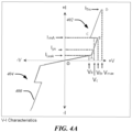
- FIG. 4A presents an exemplary current-voltage curve, shown as curve 400, for an overvoltage protection device according to embodiments of the disclosure.
- the curve 400 exhibits symmetrical behavior, including a positive voltage portion 402 and negative voltage portion 404.
- the embodiments are not limited in this context.
- the curve 400 results from the combined action of an overvoltage protection device, such as those depicted in the FIGs. 1A, 1B , 3A, and 3B .
- an overvoltage protection device such as those depicted in the FIGs. 1A, 1B , 3A, and 3B .
- the curve 400 is characterized by a breakover voltage V BR .
- the breakover current ImA may be about 400 mA, characteristic of a semiconductor crowbar device.
- the curve 400 is characteristic of an integrated overvoltage protection that resets to an OFF state once the external voltage event subsides.
- the OFF state leakage current of the curve 400 has a much lower value due to the high impedance of the semiconductor crowbar device, in comparison a simple MOV device.
- FIG. 4B presents an exemplary current-voltage curve, shown as curve 410, for a semiconductor crowbar device that may be used in an overvoltage protection device of the present embodiments.
- the curve 410 represents the current-voltage characteristic of a semiconductor crowbar device when implemented as a stand-alone component.
- Vs the semiconductor crowbar device enters an ON state and voltage reduces to a low level.
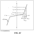
- FIG. 4C presents an exemplary current-voltage curve, shown as curve 420, for an MOV device that may be used in an overvoltage protection device of the present embodiments.
- Vnom the MOV device becomes conducting and voltage is clamped.
- the response time of an overvoltage protection device that includes an MOV and semiconductor crowbar device arranged in electrical series fashion between two electrical lines may act much faster than a standalone MOV in response to a transient voltage surge.
- Table I illustrates a comparison of experimental electrical data for an integrated overvoltage protection device of the present embodiments in comparison to a standalone MOV and standalone SIDACtor device.
- the device of the present embodiments improves clamping voltage from 850V to 492V in comparison to a standalone MOV.
- For leakage current (Idrm / Irrm) an improvement from 7.1 uA at 311 V for a standalone MOV to 0.25uA at 311 V for a device of the present embodiments is measured.
- a standalone SIDACtor provides relatively low leakage and low clamping voltage for the same test conditions, while having a large AC follow-on current.
- AC follow on current is a quantity characteristic of crowbar devices such as a SIDACtor.
- SIDACtor The rating for the follow on current for known SIDACtor devices ranges around the 230 - 270 A range (large).
- SIDACtor crowbar device
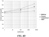
- FIG. 4D presents an exemplary breakover voltage behavior comparing a device according to the present embodiments and standalone devices.
- the breakover voltage for a standalone SIDACtor, MOV, and device according to the present embodiments are plotted as a function of rate of change in voltage with time (dV/dT).
- the SIDACTor standalone device shows a relatively flat response as a function of dV/dT
- the MOV breakover voltage is sensitive to dV/dT and increases dramatically above 100 V/ ⁇ s
- the device according to the present embodiments shows an intermediate sensitivity of breakover voltage to dV/dT. Accordingly, the present embodiments provide a faster response to a voltage impulse than a conventional MOV device.
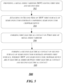
- FIG. 5 presents an exemplary process flow 500.
- the process flow 500 may be used for fabrication of an overvoltage protection device according to various embodiments of the disclosure.
- a metal oxide varistor is provided where the metal oxide varistor has a first side and second side.
- the metal oxide varistor may be fabricated from known material according to know processing techniques.
- the metal oxide varistor (MOV) may have a planar structure having a target shape such as rectangular, circular, or elliptical. The embodiments are not limited in this context.
- a first surface of a semiconductor substrate is attached to the second side of the MOV.
- the semiconductor substrate may include a semiconductor crowbar device having multiple doped semiconductor layers.
- the semiconductor crowbar device may be fabricated within a monocrystalline silicon substrate.
- the first surface of the semiconductor substrate may be attached by applying an electrically conductive material on the second side of the MOV, on the first surface of the semiconductor substrate, or on the second side of the MOV and the first surface of the semiconductor substrate.
- multiple different electrically conductive components including a coating such as conductive solder paste, such as a low temperature solder paste, metallic sheet, and the like, may be used to attach the MOV to the semiconductor substrate.
- a first electrical contact is formed on the second side of the MOV, where the second side may be opposite the first side.
- the first electrical contact may include a metal sheet or plate, a conductive paste or other components.
- a second electrical contact is formed on a second surface of the semiconductor substrate opposite the first surface.
- the first electrical contact may include a metal sheet or plate, a conductive paste or other components.
- the semiconductor crowbar device and MOV may be in electrical series with one another between the first electrical contact and the second electrical contact.
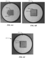
- FIGs. 6A to 6F there is shown a pictorial representation of an exemplary overvoltage protection device at various stages of fabrication, according to embodiments of the disclosure.
- a device is shown in plan view at early stages of fabrication.
- an MOV 602 is shown.
- the MOV 602 may have a circular shape in plan view, while other shapes are possible according to additional embodiments.
- a coat such as a conductive paste 604 may be applied to a surface of the MOV 602.
- a flat copper piece 606 (copper slug) may be applied to the conductive paste 604 as shown.
- the flat copper piece 606 may be formed from copper sheet, for example.
- the flat copper piece 606 may have an area that is smaller than the area of the MOV 602 as shown.
- FIG. 6B there is shown a subsequent stage when a conductive paste 608, which may be a solder paste, is applied to the outer surface of the flat copper sheet 606 away from the MOV 602. Subsequently, a semiconductor crowbar device 610 is attached to the conductive paste 608 as shown in FIG. 6B .
- the semiconductor crowbar device 610 may be embodied as a rectangular silicon chip having similar dimensions to the flat copper sheet 606.
- FIG. 6C there is shown a subsequent stage of fabrication where a conductive paste 612 may be applied to a surface of the semiconductor crowbar device 610. Subsequently, a flat copper piece 614 may be applied to the conductive paste 612 as shown.
- the flat copper piece 614 may have an area having similar dimensions to the semiconductor crowbar device 610. Together the components may form a device stack 620.
- the device stack 620 at the stage shown in FIG. 6C may be exposed to a low temperature anneal such as by hot air gun, where the temperature of hot air in the hot air gun is above room temperature.
- This low temperature anneal may promote bonding of the stack of components disposed on the MOV 602.
- FIG. 6D there is shown a top angled view of multiple overvoltage protection devices at a subsequent stage of fabrication.
- a pair of electrical leads shown as an electrical lead 622
- a conductive paste 624 may be used to attach an electrical lead 622 to the flat copper piece 614.
- Another electrical lead may be similarly attached to the side of the MOV 602 opposite the side where the semiconductor crowbar device 610 is situated.
- the other electrical lead may be attached to the opposite side forming an unannealed device before the low temperature anneal.
- FIG. 6E there is shown a side view of the overvoltage protection device at a later stage where an insulating sleeve is arranged around an electrical lead 622.
- FIG. 6F there is shown side view at a stage where an insulating coating 626, such as a plastic coating, is formed so as to encapsulate the device stack 620 as well as portions of electrical leads 622 adjacent the device stack 620.
- the insulating coating 626 may be formed by known methods for encapsulating varistors, for example. In one instance powder may be applied to the device stack and heat introduced to form a continuous coating.
Landscapes
- Engineering & Computer Science (AREA)
- Microelectronics & Electronic Packaging (AREA)
- Physics & Mathematics (AREA)
- Electromagnetism (AREA)
- Emergency Protection Circuit Devices (AREA)
- Thermistors And Varistors (AREA)
- Thyristors (AREA)
Claims (15)
- Eine Überspannungsschutzvorrichtung (100), die Folgendes beinhaltet:einen Metalloxid-Varistor, MOV, (102), der eine erste Oberfläche (114) und eine zweite Oberfläche (116) aufweist;ein Halbleitersubstrat, das eine erste äußere Oberfläche (126) und eine zweite äußere Oberfläche (128) aufweist und eine Halbleiterklemmschaltungsvorrichtung (104) beinhaltet, die eine Vielzahl von Halbleiterschichten beinhaltet, die elektrisch in Reihe zueinander angeordnet sind, wobei das Halbleitersubstrat auf einer ersten Seite (130) des MOV (102) angeordnet ist;eine leitfähige Region (124), die zwischen der zweiten Oberfläche (116) des MOV (102) und der ersten äußeren Oberfläche (126) des Halbleitersubstrats angeordnet ist;einen ersten elektrischen Kontakt (120), der auf der ersten Oberfläche (114) des MOV (102) angeordnet ist; undeinen zweiten elektrischen (122) Kontakt, der auf der zweiten äußeren Oberfläche (128) des Halbleitersubstrats angeordnet ist, dadurch gekennzeichnet, dass der MOV (102) einen ersten Teil, der einen ersten Bereich aufweist, beinhaltet, wobei das Halbleitersubstrat einen zweiten Teil, der einen im Vergleich zu dem ersten Bereich kleineren zweiten Bereich aufweist, beinhaltet.
- Überspannungsschutz(100)-Vorrichtung gemäß Anspruch 1, wobei der MOV (102) und die Halbleiterklemmschaltungsvorrichtung (104) zwischen dem ersten elektrischen Kontakt (120) und dem zweiten elektrischen Kontakt (122) elektrisch in Reihe liegen.
- Überspannungsschutzvorrichtung (100) gemäß Anspruch 1, wobei der MOV (102) eine erste Schwellenspannung beinhaltet, die Halbleiterklemmschaltungsvorrichtung (104) eine zweite Schwellenspannung beinhaltet und die Überspannungsschutzvorrichtung (100) eine Gesamtschwellenspannung beinhaltet, die gleich einer Summe der ersten Schwellenspannung und der zweiten Schwellenspannung ist.
- Überspannungsschutzvorrichtung (100) gemäß Anspruch 1, wobei der MOV (102) eine erste Ansprechzeit als eine eigenständige Vorrichtung beinhaltet und wobei die Überspannungsschutzvorrichtung eine im Vergleich zu der ersten Ansprechzeit kürzere zweite Ansprechzeit beinhaltet.
- Überspannungsschutzvorrichtung (100) gemäß Anspruch 1, wobei der MOV (102) einen ersten Leckstrom bei einer ersten Spannung als eine eigenständige Vorrichtung beinhaltet und wobei die Überspannungsschutzvorrichtung (100) einen im Vergleich zu dem ersten Leckstrom geringeren zweiten Leckstrom bei der ersten Spannung beinhaltet.
- Überspannungsschutzvorrichtung (100) gemäß Anspruch 1, wobei die Halbleiterklemmschaltungsvorrichtung (104) und der MOV (102) eingerichtet sind, um die Überspannungsschutzvorrichtung in einen EIN-Zustand zu versetzen, wenn eine externe Spannung einen Schwellenwert übersteigt, und ferner eingerichtet sind, um die Überspannungsschutzvorrichtung (100) in einen AUS-Zustand zu versetzen, wenn die externe Spannung unter dem Schwellenwert liegt.
- Überspannungsschutzvorrichtung (100) gemäß Anspruch 1, wobei die Halbleiterklemmschaltungsvorrichtung (104, 200) Folgendes beinhaltet:eine innere Schicht (204) vom n-Typ;eine erste äußere Schicht (206) vom n-Typ, die auf der ersten äußeren Oberfläche (220) angeordnet ist;eine zweite äußere Schicht (208) vom n-Typ, die auf der zweiten äußeren Oberfläche (222) angeordnet ist;eine erste Schicht (210) vom p-Typ, die zwischen der ersten äußeren Schicht (206) vom n-Typ und der inneren Schicht (204) vom n-Typ angeordnet ist; undeine zweite Schicht (212) vom p-Typ, die zwischen der zweiten äußeren Schicht (208) vom n-Typ und der inneren Schicht (204) vom n-Typ angeordnet ist.
- Überspannungsschutzvorrichtung gemäß Anspruch 7, wobei ein erster Abschnitt der ersten Schicht (210) vom p-Typ auf der ersten äußeren Oberfläche (220) angeordnet ist und ein zweiter Abschnitt der zweiten Schicht (212) vom p-Typ auf der zweiten äußeren Oberfläche (222) angeordnet ist.
- Überspannungsschutz(100)-Vorrichtung gemäß Anspruch 1, wobei die leitfähige Region (124) Folgendes beinhaltet:eine erste leitfähige Schicht, die auf der zweiten Oberfläche (114) des MOV (102) angeordnet ist;eine zweite leitfähige Schicht, die auf der ersten äußeren Oberfläche (126) des Halbleitersubstrats angeordnet ist; undein erstes Kupferstück, das zwischen der ersten leitfähigen Schicht und der zweiten leitfähigen Schicht angeordnet ist.
- Überspannungsschutzvorrichtung (100) gemäß Anspruch 1, wobei der zweite elektrische Kontakt Folgendes beinhaltet:eine dritte leitfähige Schicht, die auf der zweiten äußeren Oberfläche (128) des Halbleitersubstrats angeordnet ist; undein zweites Kupferstück, das auf der dritten leitfähigen Schicht angeordnet ist.
- Überspannungsschutzvorrichtung (100) gemäß Anspruch 1, wobei die Überspannungsschutzvorrichtung (100) eine symmetrische Vorrichtung beinhaltet, die eine erste Strom-Spannungs-Kurve als Reaktion auf eine positive externe Spannung einer ersten Größe, die zwischen dem ersten elektrischen Kontakt und dem zweiten elektrischen Kontakt angelegt wird, beinhaltet und eine zweite Strom-Spannungs-Kurve als Reaktion auf eine negative externe Spannung der ersten Größe, die zwischen dem ersten elektrischen Kontakt und dem zweiten elektrischen Kontakt angelegt wird, beinhaltet, wobei die zweite Strom-Spannungs-Kurve mit der ersten Strom-Spannungs-Kurve übereinstimmt.
- Ein Verfahren zum Herstellen einer Überspannungsschutzvorrichtung (100), das Folgendes beinhaltet:Bereitstellen eines Metalloxid-Varistors, MOV, (102, 602), der eine erste Seite und eine zweite Seite aufweist;Anbringen einer ersten Oberfläche eines Halbleitersubstrats, das eine Halbleiterklemmschaltungsvorrichtung (104) beinhaltet, an der zweiten Seite;Bilden eines ersten elektrischen Kontakts (120) auf der ersten Seite des MOV (102, 602); undBilden eines zweiten elektrischen Kontakts (122) auf einer zweiten Oberfläche des Halbleitersubstrats gegenüber der ersten Oberfläche, wobei der MOV (102) und die Halbleiterklemmschaltungsvorrichtung (104) zwischen dem ersten elektrischen Kontakt (120) und dem zweiten elektrischen Kontakt (122) elektrisch in Reihe zueinander sind, dadurch gekennzeichnet, dassder MOV (102, 602) einen ersten Teil beinhaltet, der einen ersten Bereich aufweist, wobei das Halbleitersubstrat einen zweiten Teil beinhaltet, der einen im Vergleich zu dem ersten Bereich kleineren zweiten Bereich aufweist.
- Verfahren gemäß Anspruch 12, wobei das Anbringen Folgendes beinhaltet:Aufbringen einer ersten Beschichtung, die eine Niedrigtemperatur-Lötpaste beinhaltet, auf eine erste Oberfläche (112) des MOV (102, 602);Anbringen eines ersten metallischen Teils auf der ersten Beschichtung;Aufbringen einer zweiten Beschichtung, die die Niedrigtemperatur-Lötpaste beinhaltet, auf den ersten metallischen Teil; undAnbringen des Halbleitersubstrats auf der zweiten Beschichtung.
- Verfahren gemäß Anspruch 12, wobei das Bilden des zweiten elektrischen Kontakts Folgendes beinhaltet:Aufbringen einer dritten Beschichtung, die eine Niedrigtemperatur-Lötpaste beinhaltet, auf das Halbleitersubstrat; undAnbringen eines zweiten metallischen Teils auf der dritten Beschichtung, um eine ungeglühte Vorrichtung zu bilden.
- Verfahren gemäß Anspruch 14, das ferner das Aufbringen von heißer Luft auf die ungeglühte Vorrichtung mit einer ersten Temperatur beinhaltet.
Applications Claiming Priority (1)
| Application Number | Priority Date | Filing Date | Title |
|---|---|---|---|
| PCT/CN2015/086834 WO2017024577A1 (en) | 2015-08-13 | 2015-08-13 | Overvoltage protection device |
Publications (3)
| Publication Number | Publication Date |
|---|---|
| EP3335290A1 EP3335290A1 (de) | 2018-06-20 |
| EP3335290A4 EP3335290A4 (de) | 2019-04-24 |
| EP3335290B1 true EP3335290B1 (de) | 2023-02-22 |
Family
ID=57984610
Family Applications (1)
| Application Number | Title | Priority Date | Filing Date |
|---|---|---|---|
| EP15900775.6A Active EP3335290B1 (de) | 2015-08-13 | 2015-08-13 | Überspannungsschutzvorrichtung |
Country Status (7)
| Country | Link |
|---|---|
| US (2) | US10714240B2 (de) |
| EP (1) | EP3335290B1 (de) |
| JP (1) | JP6692427B2 (de) |
| KR (1) | KR102465004B1 (de) |
| CN (2) | CN108370154A (de) |
| TW (1) | TWI711152B (de) |
| WO (1) | WO2017024577A1 (de) |
Families Citing this family (12)
| Publication number | Priority date | Publication date | Assignee | Title |
|---|---|---|---|---|
| US10411692B2 (en) | 2016-11-23 | 2019-09-10 | Alpha And Omega Semiconductor Incorporated | Active clamp overvoltage protection for switching power device |
| US10477626B2 (en) | 2016-11-23 | 2019-11-12 | Alpha And Omega Semiconductor (Cayman) Ltd. | Hard switching disable for switching power device |
| US11362513B2 (en) | 2017-03-07 | 2022-06-14 | Littelfuse Semiconductor (Wuxi) Co., Ltd. | Hybrid overvoltage protection device and assembly |
| US10476494B2 (en) | 2017-03-20 | 2019-11-12 | Alpha And Omega Semiconductor (Cayman) Ltd. | Intelligent power modules for resonant converters |
| WO2020047381A1 (en) * | 2018-08-31 | 2020-03-05 | Bourns, Inc. | Integrated device having gdt and mov functionalities |
| WO2020106964A1 (en) * | 2018-11-21 | 2020-05-28 | Abb Schweiz Ag | Voltage clamping circuit for solid state circuit breaker |
| WO2020193504A1 (en) * | 2019-03-28 | 2020-10-01 | Signify Holding B.V. | Avalanche triggered overvoltage protection |
| US11641103B2 (en) | 2020-11-06 | 2023-05-02 | Abb Schweiz Ag | Power semiconductor switch clamping circuit |
| CN118280981A (zh) * | 2022-12-30 | 2024-07-02 | 力特半导体(无锡)有限公司 | 不对称双向浪涌保护器件 |
| DE102023206991A1 (de) | 2023-07-24 | 2025-01-30 | Robert Bosch Gesellschaft mit beschränkter Haftung | Elektronische Schaltung zur Zustandsüberwachung spannungsabhängiger Widerstandsbauelemente |
| CN120184124A (zh) * | 2023-12-20 | 2025-06-20 | 力特半导体(无锡)有限公司 | 轴向引线封装结构 |
| KR102810660B1 (ko) * | 2024-04-15 | 2025-05-20 | 경상국립대학교산학협력단 | Dc 차단기의 서지전압 저감을 위한 크로우바 클램핑 회로 |
Family Cites Families (29)
| Publication number | Priority date | Publication date | Assignee | Title |
|---|---|---|---|---|
| CA96367A (en) * | 1905-10-17 | 1905-12-05 | Eustace Moriarty Weston | Rock drill mechanism |
| JPS4836333U (de) * | 1971-09-04 | 1973-05-01 | ||
| CA963167A (en) * | 1972-09-06 | 1975-02-18 | John D. Harnden (Jr.) | Hybrid circuit arrangement with metal oxide varistor shunt |
| US3898083A (en) | 1973-01-05 | 1975-08-05 | Xerox Corp | High sensitivity visible infrared photoconductor |
| JPS5231074B2 (de) * | 1973-04-20 | 1977-08-12 | ||
| JPS5234354A (en) * | 1975-09-11 | 1977-03-16 | Meidensha Electric Mfg Co Ltd | Overvoltage protector element |
| EP0315700B1 (de) | 1987-05-28 | 1994-01-05 | Matsushita Electric Industrial Co., Ltd. | Überspannungsableiter |
| JPH05234354A (ja) * | 1992-02-18 | 1993-09-10 | Nec Home Electron Ltd | Ramカード有効期限確認方式 |
| FR2709872B1 (fr) * | 1993-09-07 | 1995-11-24 | Sgs Thomson Microelectronics | Diode de shockley bidirectionnelle. |
| US5982597A (en) * | 1997-03-06 | 1999-11-09 | Webb; Rommie Fred | Shorting fusable metal oxide varistor |
| JP2003189466A (ja) * | 2001-12-13 | 2003-07-04 | Daito Communication Apparatus Co Ltd | サージ防護装置 |
| JP2006086300A (ja) * | 2004-09-15 | 2006-03-30 | Sanken Electric Co Ltd | 保護素子を有する半導体発光装置及びその製造方法 |
| EP1911047B1 (de) | 2005-07-29 | 2009-04-01 | Tyco Electronics Corporation | Schutzvorrichtung für einen schaltkreis mit wärmegekoppeltem mov-überspannungselement und pptc-überstromelement |
| CN101079341B (zh) | 2007-04-23 | 2011-06-29 | 苏州中普电子有限公司 | 不燃型压敏电阻 |
| US7741946B2 (en) * | 2007-07-25 | 2010-06-22 | Thinking Electronics Industrial Co., Ltd. | Metal oxide varistor with heat protection |
| TWI398944B (zh) | 2007-11-01 | 2013-06-11 | Alpha & Omega Semiconductor | 設有位能障式稽納二極體之低壓暫態電壓抑制器 |
| CN201393063Y (zh) * | 2009-02-02 | 2010-01-27 | 瑞侃电子(上海)有限公司 | 放电保护装置 |
| CN101800423A (zh) * | 2010-04-06 | 2010-08-11 | 常州市创捷防雷电子有限公司 | 抑制连续脉冲的电涌保护器 |
| US9570260B2 (en) * | 2011-06-17 | 2017-02-14 | Littelfuse, Inc. | Thermal metal oxide varistor circuit protection device |
| US8817433B2 (en) | 2011-07-28 | 2014-08-26 | Arm Limited | Electrostatic discharge protection device having an intermediate voltage supply for limiting voltage stress on components |
| CN102403704A (zh) * | 2011-11-16 | 2012-04-04 | 溧阳杰敏电子有限公司 | 过流过压保护器件 |
| CN202474847U (zh) * | 2011-12-28 | 2012-10-03 | 厦门赛尔特电子有限公司 | 一种交流电路的全模过压保护模组 |
| US9093831B2 (en) * | 2012-04-25 | 2015-07-28 | 4Gid Holdco Llc | Electrical wiring system and method |
| CN202695444U (zh) * | 2012-07-10 | 2013-01-23 | 上海华旭玻尔微电子有限公司 | 防静电放电器件 |
| CN203312790U (zh) | 2013-06-03 | 2013-11-27 | 厦门赛尔特电子有限公司 | 一种简易防雷模组 |
| KR101702509B1 (ko) * | 2015-03-24 | 2017-02-06 | 매이크앤 주식회사 | 황토 단열 벽체 |
| CN104779607B (zh) | 2015-04-27 | 2017-03-01 | 重庆大学 | 直流微网中的一种分布式协调控制方法及系统 |
| CN104779601A (zh) * | 2015-05-06 | 2015-07-15 | 杜尧生 | 过电压保护装置和方法 |
| JP2020080482A (ja) | 2018-11-13 | 2020-05-28 | シャープ株式会社 | ネットワークシステム、情報処理方法、通信端末、およびプログラム |
-
2015
- 2015-08-13 US US15/751,656 patent/US10714240B2/en active Active
- 2015-08-13 CN CN201580083248.1A patent/CN108370154A/zh active Pending
- 2015-08-13 EP EP15900775.6A patent/EP3335290B1/de active Active
- 2015-08-13 JP JP2018526979A patent/JP6692427B2/ja active Active
- 2015-08-13 KR KR1020187007063A patent/KR102465004B1/ko active Active
- 2015-08-13 WO PCT/CN2015/086834 patent/WO2017024577A1/en not_active Ceased
- 2015-08-13 CN CN202110478548.7A patent/CN113013861A/zh active Pending
-
2016
- 2016-08-12 TW TW105125675A patent/TWI711152B/zh active
-
2019
- 2019-12-27 US US16/728,564 patent/US10714241B2/en active Active
Also Published As
| Publication number | Publication date |
|---|---|
| JP2018533350A (ja) | 2018-11-08 |
| JP6692427B2 (ja) | 2020-05-13 |
| WO2017024577A1 (en) | 2017-02-16 |
| US20200135367A1 (en) | 2020-04-30 |
| KR102465004B1 (ko) | 2022-11-09 |
| EP3335290A1 (de) | 2018-06-20 |
| US20180240575A1 (en) | 2018-08-23 |
| TWI711152B (zh) | 2020-11-21 |
| US10714241B2 (en) | 2020-07-14 |
| CN108370154A (zh) | 2018-08-03 |
| KR20180067511A (ko) | 2018-06-20 |
| TW201717354A (zh) | 2017-05-16 |
| CN113013861A (zh) | 2021-06-22 |
| EP3335290A4 (de) | 2019-04-24 |
| US10714240B2 (en) | 2020-07-14 |
Similar Documents
| Publication | Publication Date | Title |
|---|---|---|
| US10714241B2 (en) | Overvoltage protection device | |
| CN101563784B (zh) | 低正向电压降的瞬态电压抑制器及其制造方法 | |
| US9130365B2 (en) | Method and system for ultra miniaturized packages for transient voltage suppressors | |
| US20130334695A1 (en) | Electronic device and method of manufacturing such device | |
| EP3593432B1 (de) | Hybride überspannungsschutzvorrichtung und anordnung | |
| US20090015978A1 (en) | Non-inductive silicon transient voltage suppressor | |
| US11545827B2 (en) | Surge protection apparatus having embedded fuse | |
| EP2562812A1 (de) | Integrierte Kupfersicherung in Kombination mit ESD-/Über-Spannungs-/Polaritätsumkehrschutz | |
| Urciuoli et al. | Performance of a 1-kV, silicon carbide avalanche breakdown diode | |
| CN213042916U (zh) | 一种电子装置、一种静电放电保护装置和一种半导体装置 | |
| CN101371416A (zh) | 低电容瞬变电压抑制器 | |
| US10355144B1 (en) | Heat-dissipating Zener diode | |
| US9947647B2 (en) | Method and system for over-voltage protection using transient voltage suppression devices | |
| KR102476452B1 (ko) | 사이리스터 및 열 스위치 디바이스 및 그 조립 기술 | |
| CN107301996B (zh) | 瞬态电压抑制器及其制造方法 | |
| EP2335283B1 (de) | Schutz für eine integrierte schaltung | |
| CN110323189A (zh) | 一种堆叠组合二极管保护模块 | |
| WO2025131034A1 (en) | Axial lead package structure | |
| Li et al. | Transient voltage suppressor based on diode-triggered low-voltage silicon controlled rectifier | |
| KR20130046261A (ko) | 정전기 보호용 반도체 소자의 제조방법과 그 방법에 의하여 제조되는 정전기 보호용 반도체 소자 |
Legal Events
| Date | Code | Title | Description |
|---|---|---|---|
| STAA | Information on the status of an ep patent application or granted ep patent |
Free format text: STATUS: THE INTERNATIONAL PUBLICATION HAS BEEN MADE |
|
| PUAI | Public reference made under article 153(3) epc to a published international application that has entered the european phase |
Free format text: ORIGINAL CODE: 0009012 |
|
| STAA | Information on the status of an ep patent application or granted ep patent |
Free format text: STATUS: REQUEST FOR EXAMINATION WAS MADE |
|
| 17P | Request for examination filed |
Effective date: 20180202 |
|
| AK | Designated contracting states |
Kind code of ref document: A1 Designated state(s): AL AT BE BG CH CY CZ DE DK EE ES FI FR GB GR HR HU IE IS IT LI LT LU LV MC MK MT NL NO PL PT RO RS SE SI SK SM TR |
|
| AX | Request for extension of the european patent |
Extension state: BA ME |
|
| DAV | Request for validation of the european patent (deleted) | ||
| DAX | Request for extension of the european patent (deleted) | ||
| A4 | Supplementary search report drawn up and despatched |
Effective date: 20190327 |
|
| RIC1 | Information provided on ipc code assigned before grant |
Ipc: H01C 7/12 20060101ALI20190321BHEP Ipc: H02H 9/04 20060101AFI20190321BHEP |
|
| GRAP | Despatch of communication of intention to grant a patent |
Free format text: ORIGINAL CODE: EPIDOSNIGR1 |
|
| STAA | Information on the status of an ep patent application or granted ep patent |
Free format text: STATUS: GRANT OF PATENT IS INTENDED |
|
| INTG | Intention to grant announced |
Effective date: 20220916 |
|
| GRAS | Grant fee paid |
Free format text: ORIGINAL CODE: EPIDOSNIGR3 |
|
| GRAA | (expected) grant |
Free format text: ORIGINAL CODE: 0009210 |
|
| STAA | Information on the status of an ep patent application or granted ep patent |
Free format text: STATUS: THE PATENT HAS BEEN GRANTED |
|
| AK | Designated contracting states |
Kind code of ref document: B1 Designated state(s): AL AT BE BG CH CY CZ DE DK EE ES FI FR GB GR HR HU IE IS IT LI LT LU LV MC MK MT NL NO PL PT RO RS SE SI SK SM TR |
|
| REG | Reference to a national code |
Ref country code: GB Ref legal event code: FG4D |
|
| REG | Reference to a national code |
Ref country code: CH Ref legal event code: EP |
|
| REG | Reference to a national code |
Ref country code: DE Ref legal event code: R096 Ref document number: 602015082608 Country of ref document: DE |
|
| REG | Reference to a national code |
Ref country code: AT Ref legal event code: REF Ref document number: 1550124 Country of ref document: AT Kind code of ref document: T Effective date: 20230315 Ref country code: IE Ref legal event code: FG4D |
|
| REG | Reference to a national code |
Ref country code: LT Ref legal event code: MG9D |
|
| REG | Reference to a national code |
Ref country code: NL Ref legal event code: MP Effective date: 20230222 |
|
| P01 | Opt-out of the competence of the unified patent court (upc) registered |
Effective date: 20230607 |
|
| REG | Reference to a national code |
Ref country code: AT Ref legal event code: MK05 Ref document number: 1550124 Country of ref document: AT Kind code of ref document: T Effective date: 20230222 |
|
| PG25 | Lapsed in a contracting state [announced via postgrant information from national office to epo] |
Ref country code: RS Free format text: LAPSE BECAUSE OF FAILURE TO SUBMIT A TRANSLATION OF THE DESCRIPTION OR TO PAY THE FEE WITHIN THE PRESCRIBED TIME-LIMIT Effective date: 20230222 Ref country code: PT Free format text: LAPSE BECAUSE OF FAILURE TO SUBMIT A TRANSLATION OF THE DESCRIPTION OR TO PAY THE FEE WITHIN THE PRESCRIBED TIME-LIMIT Effective date: 20230622 Ref country code: NO Free format text: LAPSE BECAUSE OF FAILURE TO SUBMIT A TRANSLATION OF THE DESCRIPTION OR TO PAY THE FEE WITHIN THE PRESCRIBED TIME-LIMIT Effective date: 20230522 Ref country code: NL Free format text: LAPSE BECAUSE OF FAILURE TO SUBMIT A TRANSLATION OF THE DESCRIPTION OR TO PAY THE FEE WITHIN THE PRESCRIBED TIME-LIMIT Effective date: 20230222 Ref country code: LV Free format text: LAPSE BECAUSE OF FAILURE TO SUBMIT A TRANSLATION OF THE DESCRIPTION OR TO PAY THE FEE WITHIN THE PRESCRIBED TIME-LIMIT Effective date: 20230222 Ref country code: LT Free format text: LAPSE BECAUSE OF FAILURE TO SUBMIT A TRANSLATION OF THE DESCRIPTION OR TO PAY THE FEE WITHIN THE PRESCRIBED TIME-LIMIT Effective date: 20230222 Ref country code: HR Free format text: LAPSE BECAUSE OF FAILURE TO SUBMIT A TRANSLATION OF THE DESCRIPTION OR TO PAY THE FEE WITHIN THE PRESCRIBED TIME-LIMIT Effective date: 20230222 Ref country code: ES Free format text: LAPSE BECAUSE OF FAILURE TO SUBMIT A TRANSLATION OF THE DESCRIPTION OR TO PAY THE FEE WITHIN THE PRESCRIBED TIME-LIMIT Effective date: 20230222 Ref country code: AT Free format text: LAPSE BECAUSE OF FAILURE TO SUBMIT A TRANSLATION OF THE DESCRIPTION OR TO PAY THE FEE WITHIN THE PRESCRIBED TIME-LIMIT Effective date: 20230222 |
|
| PG25 | Lapsed in a contracting state [announced via postgrant information from national office to epo] |
Ref country code: SE Free format text: LAPSE BECAUSE OF FAILURE TO SUBMIT A TRANSLATION OF THE DESCRIPTION OR TO PAY THE FEE WITHIN THE PRESCRIBED TIME-LIMIT Effective date: 20230222 Ref country code: PL Free format text: LAPSE BECAUSE OF FAILURE TO SUBMIT A TRANSLATION OF THE DESCRIPTION OR TO PAY THE FEE WITHIN THE PRESCRIBED TIME-LIMIT Effective date: 20230222 Ref country code: IS Free format text: LAPSE BECAUSE OF FAILURE TO SUBMIT A TRANSLATION OF THE DESCRIPTION OR TO PAY THE FEE WITHIN THE PRESCRIBED TIME-LIMIT Effective date: 20230622 Ref country code: GR Free format text: LAPSE BECAUSE OF FAILURE TO SUBMIT A TRANSLATION OF THE DESCRIPTION OR TO PAY THE FEE WITHIN THE PRESCRIBED TIME-LIMIT Effective date: 20230523 Ref country code: FI Free format text: LAPSE BECAUSE OF FAILURE TO SUBMIT A TRANSLATION OF THE DESCRIPTION OR TO PAY THE FEE WITHIN THE PRESCRIBED TIME-LIMIT Effective date: 20230222 |
|
| PG25 | Lapsed in a contracting state [announced via postgrant information from national office to epo] |
Ref country code: SM Free format text: LAPSE BECAUSE OF FAILURE TO SUBMIT A TRANSLATION OF THE DESCRIPTION OR TO PAY THE FEE WITHIN THE PRESCRIBED TIME-LIMIT Effective date: 20230222 Ref country code: RO Free format text: LAPSE BECAUSE OF FAILURE TO SUBMIT A TRANSLATION OF THE DESCRIPTION OR TO PAY THE FEE WITHIN THE PRESCRIBED TIME-LIMIT Effective date: 20230222 Ref country code: EE Free format text: LAPSE BECAUSE OF FAILURE TO SUBMIT A TRANSLATION OF THE DESCRIPTION OR TO PAY THE FEE WITHIN THE PRESCRIBED TIME-LIMIT Effective date: 20230222 Ref country code: DK Free format text: LAPSE BECAUSE OF FAILURE TO SUBMIT A TRANSLATION OF THE DESCRIPTION OR TO PAY THE FEE WITHIN THE PRESCRIBED TIME-LIMIT Effective date: 20230222 Ref country code: CZ Free format text: LAPSE BECAUSE OF FAILURE TO SUBMIT A TRANSLATION OF THE DESCRIPTION OR TO PAY THE FEE WITHIN THE PRESCRIBED TIME-LIMIT Effective date: 20230222 |
|
| REG | Reference to a national code |
Ref country code: DE Ref legal event code: R097 Ref document number: 602015082608 Country of ref document: DE |
|
| PG25 | Lapsed in a contracting state [announced via postgrant information from national office to epo] |
Ref country code: SK Free format text: LAPSE BECAUSE OF FAILURE TO SUBMIT A TRANSLATION OF THE DESCRIPTION OR TO PAY THE FEE WITHIN THE PRESCRIBED TIME-LIMIT Effective date: 20230222 |
|
| PLBE | No opposition filed within time limit |
Free format text: ORIGINAL CODE: 0009261 |
|
| STAA | Information on the status of an ep patent application or granted ep patent |
Free format text: STATUS: NO OPPOSITION FILED WITHIN TIME LIMIT |
|
| 26N | No opposition filed |
Effective date: 20231123 |
|
| PG25 | Lapsed in a contracting state [announced via postgrant information from national office to epo] |
Ref country code: SI Free format text: LAPSE BECAUSE OF FAILURE TO SUBMIT A TRANSLATION OF THE DESCRIPTION OR TO PAY THE FEE WITHIN THE PRESCRIBED TIME-LIMIT Effective date: 20230222 |
|
| PG25 | Lapsed in a contracting state [announced via postgrant information from national office to epo] |
Ref country code: MC Free format text: LAPSE BECAUSE OF FAILURE TO SUBMIT A TRANSLATION OF THE DESCRIPTION OR TO PAY THE FEE WITHIN THE PRESCRIBED TIME-LIMIT Effective date: 20230222 |
|
| REG | Reference to a national code |
Ref country code: CH Ref legal event code: PL |
|
| PG25 | Lapsed in a contracting state [announced via postgrant information from national office to epo] |
Ref country code: MC Free format text: LAPSE BECAUSE OF FAILURE TO SUBMIT A TRANSLATION OF THE DESCRIPTION OR TO PAY THE FEE WITHIN THE PRESCRIBED TIME-LIMIT Effective date: 20230222 |
|
| PG25 | Lapsed in a contracting state [announced via postgrant information from national office to epo] |
Ref country code: LU Free format text: LAPSE BECAUSE OF NON-PAYMENT OF DUE FEES Effective date: 20230813 |
|
| PG25 | Lapsed in a contracting state [announced via postgrant information from national office to epo] |
Ref country code: LU Free format text: LAPSE BECAUSE OF NON-PAYMENT OF DUE FEES Effective date: 20230813 Ref country code: CH Free format text: LAPSE BECAUSE OF NON-PAYMENT OF DUE FEES Effective date: 20230831 |
|
| REG | Reference to a national code |
Ref country code: BE Ref legal event code: MM Effective date: 20230831 |
|
| REG | Reference to a national code |
Ref country code: IE Ref legal event code: MM4A |
|
| PG25 | Lapsed in a contracting state [announced via postgrant information from national office to epo] |
Ref country code: IT Free format text: LAPSE BECAUSE OF FAILURE TO SUBMIT A TRANSLATION OF THE DESCRIPTION OR TO PAY THE FEE WITHIN THE PRESCRIBED TIME-LIMIT Effective date: 20230222 |
|
| PG25 | Lapsed in a contracting state [announced via postgrant information from national office to epo] |
Ref country code: IE Free format text: LAPSE BECAUSE OF NON-PAYMENT OF DUE FEES Effective date: 20230813 |
|
| PG25 | Lapsed in a contracting state [announced via postgrant information from national office to epo] |
Ref country code: IE Free format text: LAPSE BECAUSE OF NON-PAYMENT OF DUE FEES Effective date: 20230813 |
|
| PG25 | Lapsed in a contracting state [announced via postgrant information from national office to epo] |
Ref country code: BE Free format text: LAPSE BECAUSE OF NON-PAYMENT OF DUE FEES Effective date: 20230831 |
|
| PG25 | Lapsed in a contracting state [announced via postgrant information from national office to epo] |
Ref country code: BG Free format text: LAPSE BECAUSE OF FAILURE TO SUBMIT A TRANSLATION OF THE DESCRIPTION OR TO PAY THE FEE WITHIN THE PRESCRIBED TIME-LIMIT Effective date: 20230222 |
|
| PG25 | Lapsed in a contracting state [announced via postgrant information from national office to epo] |
Ref country code: BG Free format text: LAPSE BECAUSE OF FAILURE TO SUBMIT A TRANSLATION OF THE DESCRIPTION OR TO PAY THE FEE WITHIN THE PRESCRIBED TIME-LIMIT Effective date: 20230222 |
|
| PGFP | Annual fee paid to national office [announced via postgrant information from national office to epo] |
Ref country code: GB Payment date: 20250619 Year of fee payment: 11 |
|
| PGFP | Annual fee paid to national office [announced via postgrant information from national office to epo] |
Ref country code: FR Payment date: 20250610 Year of fee payment: 11 |
|
| PG25 | Lapsed in a contracting state [announced via postgrant information from national office to epo] |
Ref country code: CY Free format text: LAPSE BECAUSE OF FAILURE TO SUBMIT A TRANSLATION OF THE DESCRIPTION OR TO PAY THE FEE WITHIN THE PRESCRIBED TIME-LIMIT; INVALID AB INITIO Effective date: 20150813 |
|
| PG25 | Lapsed in a contracting state [announced via postgrant information from national office to epo] |
Ref country code: HU Free format text: LAPSE BECAUSE OF FAILURE TO SUBMIT A TRANSLATION OF THE DESCRIPTION OR TO PAY THE FEE WITHIN THE PRESCRIBED TIME-LIMIT; INVALID AB INITIO Effective date: 20150813 |
|
| PGFP | Annual fee paid to national office [announced via postgrant information from national office to epo] |
Ref country code: DE Payment date: 20250618 Year of fee payment: 11 |
|
| PG25 | Lapsed in a contracting state [announced via postgrant information from national office to epo] |
Ref country code: TR Free format text: LAPSE BECAUSE OF FAILURE TO SUBMIT A TRANSLATION OF THE DESCRIPTION OR TO PAY THE FEE WITHIN THE PRESCRIBED TIME-LIMIT Effective date: 20230222 |