EP3331024A1 - Halbleiterwiderstand und herstellungsverfahren dafür - Google Patents
Halbleiterwiderstand und herstellungsverfahren dafür Download PDFInfo
- Publication number
- EP3331024A1 EP3331024A1 EP17202879.7A EP17202879A EP3331024A1 EP 3331024 A1 EP3331024 A1 EP 3331024A1 EP 17202879 A EP17202879 A EP 17202879A EP 3331024 A1 EP3331024 A1 EP 3331024A1
- Authority
- EP
- European Patent Office
- Prior art keywords
- dummy gate
- gate structure
- fin
- contact area
- contact
- Prior art date
- Legal status (The legal status is an assumption and is not a legal conclusion. Google has not performed a legal analysis and makes no representation as to the accuracy of the status listed.)
- Withdrawn
Links
Images




Classifications
-
- H—ELECTRICITY
- H10—SEMICONDUCTOR DEVICES; ELECTRIC SOLID-STATE DEVICES NOT OTHERWISE PROVIDED FOR
- H10D—INORGANIC ELECTRIC SEMICONDUCTOR DEVICES
- H10D84/00—Integrated devices formed in or on semiconductor substrates that comprise only semiconducting layers, e.g. on Si wafers or on GaAs-on-Si wafers
- H10D84/201—Integrated devices formed in or on semiconductor substrates that comprise only semiconducting layers, e.g. on Si wafers or on GaAs-on-Si wafers characterised by the integration of only components covered by H10D1/00 or H10D8/00, e.g. RLC circuits
- H10D84/204—Integrated devices formed in or on semiconductor substrates that comprise only semiconducting layers, e.g. on Si wafers or on GaAs-on-Si wafers characterised by the integration of only components covered by H10D1/00 or H10D8/00, e.g. RLC circuits of combinations of diodes or capacitors or resistors
- H10D84/209—Integrated devices formed in or on semiconductor substrates that comprise only semiconducting layers, e.g. on Si wafers or on GaAs-on-Si wafers characterised by the integration of only components covered by H10D1/00 or H10D8/00, e.g. RLC circuits of combinations of diodes or capacitors or resistors of only resistors
-
- H—ELECTRICITY
- H10—SEMICONDUCTOR DEVICES; ELECTRIC SOLID-STATE DEVICES NOT OTHERWISE PROVIDED FOR
- H10W—GENERIC PACKAGES, INTERCONNECTIONS, CONNECTORS OR OTHER CONSTRUCTIONAL DETAILS OF DEVICES COVERED BY CLASS H10
- H10W44/00—Electrical arrangements for controlling or matching impedance
- H10W44/401—Resistive arrangements
-
- H—ELECTRICITY
- H10—SEMICONDUCTOR DEVICES; ELECTRIC SOLID-STATE DEVICES NOT OTHERWISE PROVIDED FOR
- H10D—INORGANIC ELECTRIC SEMICONDUCTOR DEVICES
- H10D1/00—Resistors, capacitors or inductors
- H10D1/40—Resistors
- H10D1/47—Resistors having no potential barriers
-
- H—ELECTRICITY
- H10—SEMICONDUCTOR DEVICES; ELECTRIC SOLID-STATE DEVICES NOT OTHERWISE PROVIDED FOR
- H10D—INORGANIC ELECTRIC SEMICONDUCTOR DEVICES
- H10D30/00—Field-effect transistors [FET]
- H10D30/01—Manufacture or treatment
- H10D30/021—Manufacture or treatment of FETs having insulated gates [IGFET]
- H10D30/024—Manufacture or treatment of FETs having insulated gates [IGFET] of fin field-effect transistors [FinFET]
-
- H—ELECTRICITY
- H10—SEMICONDUCTOR DEVICES; ELECTRIC SOLID-STATE DEVICES NOT OTHERWISE PROVIDED FOR
- H10D—INORGANIC ELECTRIC SEMICONDUCTOR DEVICES
- H10D30/00—Field-effect transistors [FET]
- H10D30/01—Manufacture or treatment
- H10D30/021—Manufacture or treatment of FETs having insulated gates [IGFET]
- H10D30/024—Manufacture or treatment of FETs having insulated gates [IGFET] of fin field-effect transistors [FinFET]
- H10D30/0243—Manufacture or treatment of FETs having insulated gates [IGFET] of fin field-effect transistors [FinFET] using dummy structures having essentially the same shapes as the semiconductor bodies, e.g. to provide stability
-
- H—ELECTRICITY
- H10—SEMICONDUCTOR DEVICES; ELECTRIC SOLID-STATE DEVICES NOT OTHERWISE PROVIDED FOR
- H10D—INORGANIC ELECTRIC SEMICONDUCTOR DEVICES
- H10D30/00—Field-effect transistors [FET]
- H10D30/60—Insulated-gate field-effect transistors [IGFET]
- H10D30/62—Fin field-effect transistors [FinFET]
-
- H—ELECTRICITY
- H10—SEMICONDUCTOR DEVICES; ELECTRIC SOLID-STATE DEVICES NOT OTHERWISE PROVIDED FOR
- H10D—INORGANIC ELECTRIC SEMICONDUCTOR DEVICES
- H10D84/00—Integrated devices formed in or on semiconductor substrates that comprise only semiconducting layers, e.g. on Si wafers or on GaAs-on-Si wafers
- H10D84/80—Integrated devices formed in or on semiconductor substrates that comprise only semiconducting layers, e.g. on Si wafers or on GaAs-on-Si wafers characterised by the integration of at least one component covered by groups H10D12/00 or H10D30/00, e.g. integration of IGFETs
- H10D84/811—Combinations of field-effect devices and one or more diodes, capacitors or resistors
Definitions
- the present invention relates to a technical field of semiconductors, and more particularly to a semiconductor resistor and a manufacturing method therefor.
- Fin Field Effect Transistors Fin Field Effect Transistor, FinFET are increasingly used in designs for semiconductor devices of a smaller critical dimension.
- semiconductor materials epitaxially grown on adjacent semiconductor fins may be merged.
- semiconductor materials epitaxially grown at intermediate positions of the semiconductor fins may be merged, so that the adjacent semiconductor fins may be merged.
- some of the adjacent semiconductor fins may be merged, and some may not be merged. Therefore, uniformity of the semiconductor fins is worse; this may affect the size of the finally formed semiconductor resistor.
- An objective of the present invention is relieving a phenomenon where adjacent semiconductor fins in a semiconductor resistor are merged.
- a first aspect of the present invention provides a method for manufacturing a semiconductor resistor, comprising: providing a substrate structure, wherein the substrate structure comprises a substrate having a well region and a fin structure in the well region, and wherein the fin structure comprises a semiconductor fin and an insulating layer at a surface of the semiconductor fin; forming a first dummy gate structure at an end portion of the fin structure; forming a mask layer having a first opening and a second opening, wherein the first opening exposes the first dummy gate structure and a part of the fin structure that abuts against the first dummy gate structure, and the second opening exposes another end portion of the fin structure; etching an exposed part of the fin structure using the mask layer as a mask, so as to form a first recess and a second recess; removing the mask layer, and epitaxially growing a semiconductor material in the first recess and the second recess, so as to respectively form a first contact area and a second contact area; and forming a first contact
- a side surface of the end portion of the fin structure has an isolation region; and a part of the dummy gate structure is located at the isolation region.
- the first opening further exposes a part of the isolation region.
- the method further comprises forming a second dummy gate structure at the other end portion of the fin structure; in forming the mask layer having the first opening and the second opening, the second opening exposes the second dummy gate structure and a part of the fin structure that abuts against the second dummy gate structure; in etching the exposed part of the fin structure using the mask layer as a mask, etching the exposed part of the fin structure that abuts against the first dummy gate structure and etching an exposed part of the fin structure that abuts against the second dummy gate structure , so as to form the first recess and the second recess.
- side surfaces of the two end portions of the fin structure respectively have a first isolation region and a second isolation region; a part of the first dummy gate structure is located at the first isolation region; and a part of the second dummy gate structure is located at the second isolation region.
- the first opening further exposes a part of the first isolation region
- the second opening further exposes a part of the second isolation region
- forming the first contact and the second contact in the first contact area and the second contact area includes: depositing a dielectric layer so as to cover the fin structure, the first dummy gate structure, the second dummy gate structure, the first contact area, and the second contact area; etching the dielectric layer, so as to form a first contact hole extending to the first contact area and a second contact hole extending to the second contact area; and filling in the first contact hole and the second contact hole with a metal to form the first contact and the second contact.
- the well region has a first conductivity type
- the method further includes: after the first contact area and the second contact area are formed, executing ion implantation, so that the semiconductor fin, the first contact area, and the second contact area have a second conductivity type which is different from the first conductivity type.
- a doping concentration of the first contact area and a doping concentration of the second contact area are higher than a doping concentration of the semiconductor fin.
- the fin structure includes a plurality of approximately parallel fin structures; and the first dummy gate structure and the second dummy gate structure are located at two end portions of each fin structure, respectively.
- the semiconductor material includes Si or SiGe.
- a width of the first dummy gate structure and a width of the second dummy gate structure are between 16-100 nm; a width of the first opening and a width of the second opening are between 86-200 nm; a width of the part of the fin structure that abuts against the first dummy gate structure and a width of the part of the fin structure that abuts against the second dummy gate structure are between 60-120 nm; a width of the first contact hole and a width of the second contact hole are between 40-100 nm; and a distance between the first contact hole and the first dummy gate structure and a distance between the second contact hole and the second dummy gate structure are between 15-40 nm.
- a width of the exposed part of the first isolation region and a width of the exposed part of the second isolation region are between 10-50 nm.
- a second aspect of the present invention provides a semiconductor resistor.
- the semiconductor device comprises: a substrate having a well region and a fin structure in the well region, wherein the fin structure comprises a semiconductor fin and an insulating layer at a surface of the semiconductor fin; a first dummy gate structure at an end portion of the fin structure; a first contact area which abuts against the first dummy gate structure, wherein a part of the first contact area is located in the semiconductor fin; a second contact area, wherein a part of the second contact area is located in another end portion of the semiconductor fin; a first contact connected to the first contact area; and a second contact connected to the second contact area.
- a side surface of the end portion of the fin structure has an isolation region; and a part of the dummy gate structure is located at the isolation region.
- the first dummy gate structure and a second dummy gate structure at two end portions of the fin structure; a second contact area which abuts against the second dummy gate structure, wherein a part of the second contact area is positioned in the semiconductor fin.
- side surfaces of the two end portions of the fin structure respectively have a first isolation region and a second isolation region; a part of the first dummy gate structure is located at the first isolation region; and a part of the second dummy gate structure is located at the second isolation region.
- the well region has a first conductivity type; and the semiconductor fin, the first contact area, and the second contact area have a second conductivity type.
- a doping concentration of the first contact area and a doping concentration of the second contact area are higher than a doping concentration of the semiconductor fin.
- the fin structure includes a plurality of approximately parallel fin structures; and the first dummy gate structure and the second dummy gate structure are located at two end portions of each fin structure, respectively.
- materials of the first contact area and the second contact area include Si or SiGe.
- a width of the first dummy gate structure and a width of the second dummy gate structure are between 16-100 nm; a width of the first contact area and a width of the second contact area are between 60-120 nm; a width of the first contact and a width of the second contact are between 40-100 nm; and a distance between the first contact and the first dummy gate structure and a distance between the second contact and the second dummy gate structure are between 15-40 nm.
- the resistor according to the second aspect of the present invention may be obtained by a method according to the first aspect of the present invention.
- dummy gate structures are formed at two ends of a fin structure, where the dummy gate structures may change appearances of epitaxially formed first contact area and second contact area.
- a position of an etched area is defined by using a first opening and a second opening of a mask layer, and only parts of the fin structure that abut against the first dummy gate structure and the second dummy gate structure are etched. Therefore, an epitaxially formed contact area is located at two end portions of the fin structure instead of the entire upper portion of the fin structure. In this way, a probability that the epitaxially formed contact area merges with contact areas of other fin structures is reduced. Therefore, forms of the present invention may relieve a phenomenon that adjacent semiconductor fins in a semiconductor resistor are merged, and improve uniformity of the semiconductor fins in the semiconductor resistor. Moreover, the manufacturing method of the present invention is compatible with the FinFET process.
- FIG. 1 is a simplified flowchart of one form of a method for manufacturing a semiconductor resistor. As shown in FIG. 1 , in step 102, a substrate structure is provided.
- FIG. 2A shows a section drawing of a substrate structure according to one form of the present invention.
- the substrate structure may include a substrate having a well region 201 and a fin structure 202 in the region 201.
- the fin structure 202 includes a semiconductor fin 212 and an insulating layer 222 at a surface of the semiconductor fin 212.
- Material of the semiconductor fin 212 may be a semiconductor material such as silicon or germanium.
- Material of the insulating layer 222 may be, for example, an oxide of silicon.
- side surfaces of two end portions of the fin structure 202 may respectively have a first isolation region 203 and a second isolation region 204, for example, a shallow trench isolation (STI) region.
- STI shallow trench isolation
- the fin structure 202 may include a plurality of approximately parallel fin structures (not shown).
- the plurality of fin structures may be arranged to be approximately parallel along a direction vertical to the paper surface.
- An isolation region for example, a shallow trench isolation (STI) region, may be provided between adjacent fin structures.
- STI shallow trench isolation
- a first dummy gate structure 301 and a second dummy gate structure 302 are formed at the two end portions of the fin structure 202, respectively.
- a dummy gate material such as polysilicon
- a patterned hard mask may be formed on the dummy gate material, and after that, the dummy gate material is etched by using the patterned hard mask as a mask. In this way, the first dummy gate structure 301 and the second dummy gate structure 302 are formed.
- the first dummy gate structure 301 may include a first dummy gate and a first hard mask on the first dummy gate
- the second dummy gate structure 302 may include a second dummy gate and a second hard mask on the second dummy gate.
- the first dummy gate structure 301 may also merely include a first dummy gate
- the second dummy gate structure 302 may also merely include a second dummy gate.
- the fin structure 202 includes a plurality of fin structures
- the formed first dummy gate structure 301 and second dummy gate structure 302 are located at two end portions of each fin structure, respectively. That is, the first dummy gate structure 301 and the second dummy gate structure 302 span the two end portions of each fin structure.
- a part of the first dummy gate structure 301 may be located at the first isolation region 203, and other parts of the first dummy gate structure 301 span over an end portion of the fin structure 202; and a part of the second dummy gate structure 302 may be located at the second isolation region 204, and other parts of the second dummy gate structure 302 span the other end portion of the fin structure 202.
- the first dummy gate structure 301 and the second dummy gate structure 302 may completely span over the two end portions of the fin structure 202 (not shown in the drawings).
- step 106 form a mask layer 401 having a first opening 411 and a second opening 421 on the structure shown in FIG. 3 , for example, photoresist.
- the first opening 411 may expose the first dummy gate structure 301 and a part of the fin structure 202 that abuts against the first dummy gate structure 301.
- the second opening 421 may expose the second dummy gate structure 302 and a part of the fin structure 202 that abuts against the second dummy gate structure 302.
- the first opening 411 may further expose a part of the first isolation region 203
- the second opening 421 may further expose a part of the second isolation region 204.
- widths of the exposed part of the first isolation region 203 and the exposed part of the second isolation region 204 may be about 10-50 nm, for example, 30 nm or 40 nm.
- step 108 the exposed parts of the fin structure 202 are etched using the mask layer 401 as a mask, so as to form a first recess 501 and a second recess 502, as shown in FIG. 5 .
- the first dummy gate structure 301 and the second dummy gate structure 302 are also used as a mask, respectively.
- step 110 the mask layer 401 is removed, and an epitaxially grown semiconductor material, such as Si or SiGe, is epitaxially grown in the first recess 501 and the second recess 502, so as to respectively form a first contact area 601 and a second contact area 602, as shown in FIG. 6 .
- an epitaxially grown semiconductor material such as Si or SiGe
- parts of the first contact area 601 and the second contact area 602 may be located within the semiconductor fin 212, and parts may protrude outside the semiconductor fin 212.
- the first contact area 601 and the second contact area 602 may also be called as raised first contact area 601 and second contact area 602.
- ion implantation may further be executed, so that the semiconductor fin 212, the first contact area 601, and the second contact area 602 have a second conductivity type which is different from the first conductivity type.
- the well region is a N well, and the semiconductor fin 212, the first contact area 601, and the second contact area 602 are P+ doped.
- the well region is a P well, and the semiconductor fin 212, the first contact area 601, and the second contact area 602 are N+ doped.
- doping concentrations of the first contact area 601 and the second contact area 602 are higher than a doping concentration of the semiconductor fin 212. Therefore, contact resistance when forming a contact may be reduced.
- a first contact connected to the first contact area 601 and a second contact connected to the second contact area 602 are formed.
- the first contact and the second contact may be formed according to the manner shown in FIG. 7 to FIG. 9 .
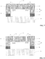
- a dielectric layer 701 for example, an oxide of silicon, is deposited so as to cover the fin structure 202, the first dummy gate structure 301, the second dummy gate structure 302, the first contact area 601, and the second contact area 602.
- the dielectric layer 701 is etched, so as to form a first contact hole 801 extending to the first contact area 601 and a second contact hole 802 extending to the second contact area 602.
- a patterned hard mask may be formed on the dielectric layer 701, so as to define shapes of the first contact hole and the second contact hole; and then the dielectric layer 701 is etched by using the patterned hard mask as a mask, so as to form the first contact hole 801 and the second contact hole 802.
- widths of the first contact hole and the second contact hole may be about 40-100 nm, for example, 60 nm or 80 nm; and a distance between the first contact hole 801 and the first dummy gate structure 301 and a distance between the second contact hole 802 and the second dummy gate structure 302 may be about 15-40 nm, for example, 20 nm or 30 nm.
- a metal such as tungsten, is filled in the first contact hole 801 and the second contact hole 802, so as to form a first contact 901 and the second contact 902.
- Implementations of a method for manufacturing a semiconductor resistor is described above.
- the method provided forms dummy gate structures at two ends of a fin structure, where the dummy gate structures may change appearances of epitaxially formed first contact area and second contact area.
- a position of an etched area is defined using a first opening and a second opening of a mask layer, and only parts of the fin structure that abut against the first dummy gate structure and the second dummy gate structure are etched. Therefore, an epitaxially formed contact area is merely located at two end portions of the fin structure instead of the entire upper portion of the fin structure. In this way, the probability that the epitaxially formed contact area merges with contact areas of other fin structures is reduced. Therefore, this implementation may relieve a phenomenon that adjacent semiconductor fins in a semiconductor resistor are merged, and improve uniformity of the semiconductor fins in the semiconductor resistor.
- the manufacturing method of this implementation is compatible with a FinFET process.
- appearance of the second contact area 602 may be optimized, so as to better reduce the phenomenon that adjacent semiconductor fins in a semiconductor resistor are merged.
- widths of the first dummy gate structure 301 and the second dummy gate structure 302 may be about 16-100 nm, for example, 30 nm, 50 nm, or 70 nm.
- widths of the first opening 411 and the second opening 421 may be about 86-200 nm, for example, 100 nm, 150 nm, or 180 nm.
- widths of a part of the fin structure 202 that abuts against the first dummy gate structure 301 and a part of the fin structure 202 that abuts against the second dummy gate structure 302 may be about 60-120 nm, for example, 80 nm or 90 nm.
- the present invention further provides a semiconductor resistor.
- the semiconductor resistor may include a substrate having a well region 201 and a fin structure 202 in the region 201.
- the fin structure 202 may include a semiconductor fin 212 and an insulating layer 222 at a surface of the semiconductor fin 212.
- the fin structure may include a plurality of approximately parallel fin structures (description is made below with reference to FIG. 10 ).
- the semiconductor resistor may further include a first dummy gate structure 301 and a second dummy gate structure 302 at two end portions of the fin structure 202.
- side surfaces of the two end portions of the fin structure may respectively have a first isolation region 203 and a second isolation region 204, where a part of the first dummy gate structure 301 may be located at the first isolation region 203, and a part of the second dummy gate structure 302 may be located at the second isolation region 204.
- the semiconductor resistor may further include a first contact area 601, a second contact area 602, a first contact 901 connected to the first contact area 601, and a second contact 902 connected to the second contact area 602.
- first contact area 601 abuts against the first dummy gate structure 301
- a part of the first contact area 601 is located in the semiconductor fin 212, and a part thereof protrudes outside the semiconductor fin 212.
- second contact area 602 abuts against the second dummy gate structure 302, a part of the second contact area 602 is located in the semiconductor fin 212, and a part thereof protrudes outside the semiconductor fin 212.
- Materials of the first contact area 601 and the second contact area 602 may include, for example, Si or SiGe.
- the well region 201 may have a first conductivity type
- the semiconductor fin 212, the first contact area 601, and the second contact area 602 may have a second conductivity type.
- doping concentrations of the first contact area 601 and the second contact area 602 are higher than a doping concentration of the semiconductor fin 212.
- FIG. 10 shows a top view schematic diagram of one form of a semiconductor resistor including a plurality of fin structures.
- the first dummy gate structure 301 and the second dummy gate structure 302 are located at two end portions of each fin structure, respectively.
- the first contact 901 is connected to the first contact area 601 in each fin structure, and the second contact 902 is connected to the second contact area 602 in each fin structure.
- a size of a semiconductor resistor may be adjusted by adjusting the quantity of fin structures. For example, when an expected resistance value is great, a small number of fin structures may be used, for example, using one fin structure; and when the expected resistance value is small, a large number of fin structures may be used, for example, using two or more fin structures, so as to satisfy the requirements of the resistance value.
- the semiconductor resistor provided in the present invention includes a plurality of fin structures, because adjacent semiconductor fins would not be merged, the quantity of the fin structures may be controlled more easily according to the size of the semiconductor resistor.
- widths of the first dummy gate structure 301 and the second dummy gate structure 302 are about 16-100 nm, for example, 30 nm, 50 nm, or 70 nm. In some implementations, widths of the first contact area 601 and the second contact area 602 are about 60-120 nm, for example, 80 nm or 90 nm. In some implementations, widths of the first contact 901 and the second contact 902 are about 40-100 nm, for example, 60 nm or 80 nm.
- a distance between the first contact 901 and the first dummy gate structure 301 and a distance between the second contact 902 and the second dummy gate structure 302 are about 15-40 nm, for example, 20 nm or 30 nm.
- FIG. 11 is a simplified flowchart of one form of a method for manufacturing a semiconductor resistor. As shown in FIG. 11 , the manufacturing method may include the following steps:
- the method provided in this implementation only forms a dummy gate structure at an end of a fin structure, where the dummy gate structure may change appearance of an epitaxially formed first contact area.
- a position of an etched area is defined using a first opening and a second opening of a mask layer, and only a part of the fin structure that abuts against the dummy gate structure and the other end portion of the fin structure are etched. Therefore, an epitaxially formed contact area is merely located at two end portions of the fin structure instead of the entire upper portion of the fin structure. In this way, the probability that the contact area merges with contact areas of other fin structures is reduced. Therefore, implementations of this manufacturing method may also relieve a phenomenon that adjacent semiconductor fins in a semiconductor resistor are merged, and improve uniformity of the semiconductor fins in the semiconductor resistor. Moreover, implementations of this manufacturing method is compatible with a FinFET process.
- the present invention further provides another semiconductor resistor, including a substrate having a well region and a fin structure in the region.
- the fin structure includes a semiconductor fin and an insulating layer at a surface of the semiconductor fin.
- the semiconductor resistor further includes a dummy gate structure at an end portion of the fin structure.
- a side surface of an end portion of fin structure may be provided with an isolation region on which a part of the dummy gate structure may be located.
- the semiconductor resistor may further include a first contact area, a second contact area, a first contact connected to the first contact area, and a second contact connected to the second contact area.
- the first contact area abuts against the dummy gate structure, and a part of the first contact area is located in the semiconductor fin.
- a part of the second contact area is located in another end portion of the semiconductor fin.
Landscapes
- Metal-Oxide And Bipolar Metal-Oxide Semiconductor Integrated Circuits (AREA)
- Insulated Gate Type Field-Effect Transistor (AREA)
- Semiconductor Integrated Circuits (AREA)
Applications Claiming Priority (1)
| Application Number | Priority Date | Filing Date | Title |
|---|---|---|---|
| CN201611046393.5A CN108091639B (zh) | 2016-11-23 | 2016-11-23 | 半导体电阻及其制造方法 |
Publications (1)
| Publication Number | Publication Date |
|---|---|
| EP3331024A1 true EP3331024A1 (de) | 2018-06-06 |
Family
ID=60450449
Family Applications (1)
| Application Number | Title | Priority Date | Filing Date |
|---|---|---|---|
| EP17202879.7A Withdrawn EP3331024A1 (de) | 2016-11-23 | 2017-11-21 | Halbleiterwiderstand und herstellungsverfahren dafür |
Country Status (3)
| Country | Link |
|---|---|
| US (1) | US10553579B2 (de) |
| EP (1) | EP3331024A1 (de) |
| CN (1) | CN108091639B (de) |
Families Citing this family (2)
| Publication number | Priority date | Publication date | Assignee | Title |
|---|---|---|---|---|
| CN110875255B (zh) * | 2018-08-29 | 2022-07-01 | 中芯国际集成电路制造(上海)有限公司 | 半导体器件及其形成方法 |
| CN121865646A (zh) * | 2024-10-10 | 2026-04-14 | 无锡华润微电子有限公司 | 一种半导体器件及其制造方法、电子装置 |
Citations (3)
| Publication number | Priority date | Publication date | Assignee | Title |
|---|---|---|---|---|
| US20100013026A1 (en) * | 2008-07-15 | 2010-01-21 | International Business Machines Corporation | Integrated circuits comprising resistors having different sheet resistances and methods of fabricating the same |
| US20120175749A1 (en) * | 2011-01-06 | 2012-07-12 | International Business Machines Corporation | Structure and Method to Fabricate Resistor on FinFET Processes |
| US20130292777A1 (en) * | 2012-05-03 | 2013-11-07 | Taiwan Semiconductor Manufacturing Company, Ltd. | Structure for FinFETs |
Family Cites Families (16)
| Publication number | Priority date | Publication date | Assignee | Title |
|---|---|---|---|---|
| US6720231B2 (en) * | 2002-01-28 | 2004-04-13 | International Business Machines Corporation | Fin-type resistors |
| DE10206375A1 (de) * | 2002-02-15 | 2003-06-26 | Infineon Technologies Ag | Integrierte, abstimmbare Kapazität |
| US8890260B2 (en) * | 2009-09-04 | 2014-11-18 | Taiwan Semiconductor Manufacturing Company, Ltd. | Polysilicon design for replacement gate technology |
| US8043920B2 (en) * | 2009-09-17 | 2011-10-25 | International Business Machines Corporation | finFETS and methods of making same |
| KR20140021080A (ko) * | 2012-07-16 | 2014-02-20 | 삼성전자주식회사 | 반도체 장치 및 그 제조 방법 |
| FR2995722B1 (fr) * | 2012-09-17 | 2015-07-17 | Soitec Silicon On Insulator | Finfet en silicium sur isolant avec une dependance reduite vis-a-vis de la largeur du fin |
| US8962421B2 (en) * | 2012-11-15 | 2015-02-24 | GlobalFoundries, Inc. | Methods for fabricating integrated circuits including semiconductive resistor structures in a FinFET architecture |
| US9111780B2 (en) * | 2013-03-12 | 2015-08-18 | Taiwan Semiconductor Manufacturing Company, Ltd. | Structure and method for vertical tunneling field effect transistor with leveled source and drain |
| US20150061076A1 (en) * | 2013-08-27 | 2015-03-05 | International Business Machines Corporation | High density resistor |
| KR102085525B1 (ko) * | 2013-11-27 | 2020-03-09 | 삼성전자 주식회사 | 반도체 장치 및 그 제조 방법 |
| CN104681557B (zh) * | 2013-11-28 | 2018-02-06 | 中国科学院微电子研究所 | 半导体装置及其制造方法 |
| US9524962B2 (en) * | 2013-12-20 | 2016-12-20 | Globalfoundries Inc. | Semiconductor device comprising an e-fuse and a FET |
| US9614023B2 (en) * | 2014-12-29 | 2017-04-04 | Globalfoundries Inc. | Substrate resistor with overlying gate structure |
| US9613953B2 (en) * | 2015-03-24 | 2017-04-04 | Taiwan Semiconductor Manufacturing Company, Ltd. | Semiconductor device, semiconductor device layout, and method of manufacturing semiconductor device |
| US9576979B2 (en) * | 2015-05-27 | 2017-02-21 | International Business Machines Corporation | Preventing strained fin relaxation by sealing fin ends |
| US9997590B2 (en) * | 2016-10-24 | 2018-06-12 | International Büsiness Machines Corporation | FinFET resistor and method to fabricate same |
-
2016
- 2016-11-23 CN CN201611046393.5A patent/CN108091639B/zh active Active
-
2017
- 2017-08-22 US US15/683,166 patent/US10553579B2/en active Active
- 2017-11-21 EP EP17202879.7A patent/EP3331024A1/de not_active Withdrawn
Patent Citations (3)
| Publication number | Priority date | Publication date | Assignee | Title |
|---|---|---|---|---|
| US20100013026A1 (en) * | 2008-07-15 | 2010-01-21 | International Business Machines Corporation | Integrated circuits comprising resistors having different sheet resistances and methods of fabricating the same |
| US20120175749A1 (en) * | 2011-01-06 | 2012-07-12 | International Business Machines Corporation | Structure and Method to Fabricate Resistor on FinFET Processes |
| US20130292777A1 (en) * | 2012-05-03 | 2013-11-07 | Taiwan Semiconductor Manufacturing Company, Ltd. | Structure for FinFETs |
Also Published As
| Publication number | Publication date |
|---|---|
| CN108091639A (zh) | 2018-05-29 |
| US20180145069A1 (en) | 2018-05-24 |
| US10553579B2 (en) | 2020-02-04 |
| CN108091639B (zh) | 2020-05-08 |
Similar Documents
| Publication | Publication Date | Title |
|---|---|---|
| US10388792B2 (en) | FinFET with rounded source/drain profile | |
| US8143114B2 (en) | System and method for source/drain contact processing | |
| CN103311124B (zh) | 半导体器件及其制造方法 | |
| TWI540727B (zh) | 鰭式場效電晶體元件之鰭結構、鰭式場效電晶體元件 | |
| US9954104B2 (en) | Multiwidth finFET with channel cladding | |
| KR101624388B1 (ko) | 채널 에피택셜 영역을 갖는 finfet 디바이스 | |
| US10497810B2 (en) | Method for fabricating semiconductor device | |
| TW201839814A (zh) | 半導體元件之形成方法 | |
| US20180151371A1 (en) | Semiconductor device and fabrication method thereof | |
| TW202032634A (zh) | 半導體裝置的製作方法 | |
| EP3316286A1 (de) | Dummy-gatestrukturen und verfahren zu ihrer herstellung | |
| US9437713B2 (en) | Devices and methods of forming higher tunability FinFET varactor | |
| US7399690B2 (en) | Methods of fabricating semiconductor devices and structures thereof | |
| US20190221639A1 (en) | Nanosheet device and method for fabricating the same | |
| US10553579B2 (en) | Semiconductor resistor and manufacturing method therefor | |
| CN108470769A (zh) | 鳍式晶体管及其制造方法 | |
| US9166025B1 (en) | Methods of forming a nanowire device with a gate-all-around-channel configuration and the resulting nanowire device | |
| US10381464B2 (en) | Method for manufacturing semiconductor device | |
| KR102450329B1 (ko) | 마스크 설계 방법 및 이를 이용한 반도체 장치 제조 방법 | |
| US11264488B2 (en) | Manufacturing method of semiconductor structure | |
| US12439652B2 (en) | MOS device with sandwich structure and groove | |
| TW202441596A (zh) | 半導體元件及其製作方法 | |
| CN102820320B (zh) | 半绝缘体上硅半导体器件及其制造方法 |
Legal Events
| Date | Code | Title | Description |
|---|---|---|---|
| PUAI | Public reference made under article 153(3) epc to a published international application that has entered the european phase |
Free format text: ORIGINAL CODE: 0009012 |
|
| STAA | Information on the status of an ep patent application or granted ep patent |
Free format text: STATUS: THE APPLICATION HAS BEEN PUBLISHED |
|
| AK | Designated contracting states |
Kind code of ref document: A1 Designated state(s): AL AT BE BG CH CY CZ DE DK EE ES FI FR GB GR HR HU IE IS IT LI LT LU LV MC MK MT NL NO PL PT RO RS SE SI SK SM TR |
|
| AX | Request for extension of the european patent |
Extension state: BA ME |
|
| RAP1 | Party data changed (applicant data changed or rights of an application transferred) |
Owner name: SEMICONDUCTOR MANUFACTURING INTERNATIONAL (BEIJING Owner name: SEMICONDUCTOR MANUFACTURING INTERNATIONAL (SHANGHA |
|
| STAA | Information on the status of an ep patent application or granted ep patent |
Free format text: STATUS: REQUEST FOR EXAMINATION WAS MADE |
|
| 17P | Request for examination filed |
Effective date: 20181206 |
|
| RBV | Designated contracting states (corrected) |
Designated state(s): AL AT BE BG CH CY CZ DE DK EE ES FI FR GB GR HR HU IE IS IT LI LT LU LV MC MK MT NL NO PL PT RO RS SE SI SK SM TR |
|
| STAA | Information on the status of an ep patent application or granted ep patent |
Free format text: STATUS: EXAMINATION IS IN PROGRESS |
|
| 17Q | First examination report despatched |
Effective date: 20210614 |
|
| STAA | Information on the status of an ep patent application or granted ep patent |
Free format text: STATUS: THE APPLICATION IS DEEMED TO BE WITHDRAWN |
|
| 18D | Application deemed to be withdrawn |
Effective date: 20211026 |