EP3327776A2 - Halbleiterstruktur, statischer direktzugriffsspeicher und herstellungsverfahren dafür - Google Patents
Halbleiterstruktur, statischer direktzugriffsspeicher und herstellungsverfahren dafür Download PDFInfo
- Publication number
- EP3327776A2 EP3327776A2 EP17202701.3A EP17202701A EP3327776A2 EP 3327776 A2 EP3327776 A2 EP 3327776A2 EP 17202701 A EP17202701 A EP 17202701A EP 3327776 A2 EP3327776 A2 EP 3327776A2
- Authority
- EP
- European Patent Office
- Prior art keywords
- pass gate
- fin
- transistor region
- region
- gate transistor
- Prior art date
- Legal status (The legal status is an assumption and is not a legal conclusion. Google has not performed a legal analysis and makes no representation as to the accuracy of the status listed.)
- Withdrawn
Links
Images


Classifications
-
- H—ELECTRICITY
- H10—SEMICONDUCTOR DEVICES; ELECTRIC SOLID-STATE DEVICES NOT OTHERWISE PROVIDED FOR
- H10D—INORGANIC ELECTRIC SEMICONDUCTOR DEVICES
- H10D30/00—Field-effect transistors [FET]
- H10D30/60—Insulated-gate field-effect transistors [IGFET]
- H10D30/62—Fin field-effect transistors [FinFET]
- H10D30/6215—Fin field-effect transistors [FinFET] having multiple independently-addressable gate electrodes
-
- G—PHYSICS
- G11—INFORMATION STORAGE
- G11C—STATIC STORES
- G11C11/00—Digital stores characterised by the use of particular electric or magnetic storage elements; Storage elements therefor
- G11C11/21—Digital stores characterised by the use of particular electric or magnetic storage elements; Storage elements therefor using electric elements
- G11C11/34—Digital stores characterised by the use of particular electric or magnetic storage elements; Storage elements therefor using electric elements using semiconductor devices
- G11C11/40—Digital stores characterised by the use of particular electric or magnetic storage elements; Storage elements therefor using electric elements using semiconductor devices using transistors
- G11C11/401—Digital stores characterised by the use of particular electric or magnetic storage elements; Storage elements therefor using electric elements using semiconductor devices using transistors forming cells needing refreshing or charge regeneration, i.e. dynamic cells
- G11C11/402—Digital stores characterised by the use of particular electric or magnetic storage elements; Storage elements therefor using electric elements using semiconductor devices using transistors forming cells needing refreshing or charge regeneration, i.e. dynamic cells with charge regeneration individual to each memory cell, i.e. internal refresh
- G11C11/4023—Digital stores characterised by the use of particular electric or magnetic storage elements; Storage elements therefor using electric elements using semiconductor devices using transistors forming cells needing refreshing or charge regeneration, i.e. dynamic cells with charge regeneration individual to each memory cell, i.e. internal refresh using field effect transistors
-
- H—ELECTRICITY
- H10—SEMICONDUCTOR DEVICES; ELECTRIC SOLID-STATE DEVICES NOT OTHERWISE PROVIDED FOR
- H10B—ELECTRONIC MEMORY DEVICES
- H10B10/00—Static random access memory [SRAM] devices
- H10B10/12—Static random access memory [SRAM] devices comprising a MOSFET load element
-
- H—ELECTRICITY
- H10—SEMICONDUCTOR DEVICES; ELECTRIC SOLID-STATE DEVICES NOT OTHERWISE PROVIDED FOR
- H10D—INORGANIC ELECTRIC SEMICONDUCTOR DEVICES
- H10D30/00—Field-effect transistors [FET]
- H10D30/01—Manufacture or treatment
- H10D30/021—Manufacture or treatment of FETs having insulated gates [IGFET]
- H10D30/024—Manufacture or treatment of FETs having insulated gates [IGFET] of fin field-effect transistors [FinFET]
-
- H—ELECTRICITY
- H10—SEMICONDUCTOR DEVICES; ELECTRIC SOLID-STATE DEVICES NOT OTHERWISE PROVIDED FOR
- H10D—INORGANIC ELECTRIC SEMICONDUCTOR DEVICES
- H10D30/00—Field-effect transistors [FET]
- H10D30/60—Insulated-gate field-effect transistors [IGFET]
- H10D30/62—Fin field-effect transistors [FinFET]
- H10D30/6211—Fin field-effect transistors [FinFET] having fin-shaped semiconductor bodies integral with the bulk semiconductor substrates
-
- H—ELECTRICITY
- H10—SEMICONDUCTOR DEVICES; ELECTRIC SOLID-STATE DEVICES NOT OTHERWISE PROVIDED FOR
- H10D—INORGANIC ELECTRIC SEMICONDUCTOR DEVICES
- H10D30/00—Field-effect transistors [FET]
- H10D30/60—Insulated-gate field-effect transistors [IGFET]
- H10D30/62—Fin field-effect transistors [FinFET]
- H10D30/6219—Fin field-effect transistors [FinFET] characterised by the source or drain electrodes
-
- H—ELECTRICITY
- H10—SEMICONDUCTOR DEVICES; ELECTRIC SOLID-STATE DEVICES NOT OTHERWISE PROVIDED FOR
- H10D—INORGANIC ELECTRIC SEMICONDUCTOR DEVICES
- H10D62/00—Semiconductor bodies, or regions thereof, of devices having potential barriers
- H10D62/10—Shapes, relative sizes or dispositions of the regions of the semiconductor bodies; Shapes of the semiconductor bodies
-
- H—ELECTRICITY
- H10—SEMICONDUCTOR DEVICES; ELECTRIC SOLID-STATE DEVICES NOT OTHERWISE PROVIDED FOR
- H10D—INORGANIC ELECTRIC SEMICONDUCTOR DEVICES
- H10D62/00—Semiconductor bodies, or regions thereof, of devices having potential barriers
- H10D62/10—Shapes, relative sizes or dispositions of the regions of the semiconductor bodies; Shapes of the semiconductor bodies
- H10D62/124—Shapes, relative sizes or dispositions of the regions of semiconductor bodies or of junctions between the regions
-
- H—ELECTRICITY
- H10—SEMICONDUCTOR DEVICES; ELECTRIC SOLID-STATE DEVICES NOT OTHERWISE PROVIDED FOR
- H10D—INORGANIC ELECTRIC SEMICONDUCTOR DEVICES
- H10D62/00—Semiconductor bodies, or regions thereof, of devices having potential barriers
- H10D62/10—Shapes, relative sizes or dispositions of the regions of the semiconductor bodies; Shapes of the semiconductor bodies
- H10D62/13—Semiconductor regions connected to electrodes carrying current to be rectified, amplified or switched, e.g. source or drain regions
- H10D62/149—Source or drain regions of field-effect devices
- H10D62/151—Source or drain regions of field-effect devices of IGFETs
-
- H—ELECTRICITY
- H10—SEMICONDUCTOR DEVICES; ELECTRIC SOLID-STATE DEVICES NOT OTHERWISE PROVIDED FOR
- H10D—INORGANIC ELECTRIC SEMICONDUCTOR DEVICES
- H10D62/00—Semiconductor bodies, or regions thereof, of devices having potential barriers
- H10D62/80—Semiconductor bodies, or regions thereof, of devices having potential barriers characterised by the materials
- H10D62/82—Heterojunctions
- H10D62/822—Heterojunctions comprising only Group IV materials heterojunctions, e.g. Si/Ge heterojunctions
-
- H—ELECTRICITY
- H10—SEMICONDUCTOR DEVICES; ELECTRIC SOLID-STATE DEVICES NOT OTHERWISE PROVIDED FOR
- H10D—INORGANIC ELECTRIC SEMICONDUCTOR DEVICES
- H10D84/00—Integrated devices formed in or on semiconductor substrates that comprise only semiconducting layers, e.g. on Si wafers or on GaAs-on-Si wafers
- H10D84/80—Integrated devices formed in or on semiconductor substrates that comprise only semiconducting layers, e.g. on Si wafers or on GaAs-on-Si wafers characterised by the integration of at least one component covered by groups H10D12/00 or H10D30/00, e.g. integration of IGFETs
- H10D84/82—Integrated devices formed in or on semiconductor substrates that comprise only semiconducting layers, e.g. on Si wafers or on GaAs-on-Si wafers characterised by the integration of at least one component covered by groups H10D12/00 or H10D30/00, e.g. integration of IGFETs of only field-effect components
- H10D84/83—Integrated devices formed in or on semiconductor substrates that comprise only semiconducting layers, e.g. on Si wafers or on GaAs-on-Si wafers characterised by the integration of at least one component covered by groups H10D12/00 or H10D30/00, e.g. integration of IGFETs of only field-effect components of only insulated-gate FETs [IGFET]
- H10D84/834—Integrated devices formed in or on semiconductor substrates that comprise only semiconducting layers, e.g. on Si wafers or on GaAs-on-Si wafers characterised by the integration of at least one component covered by groups H10D12/00 or H10D30/00, e.g. integration of IGFETs of only field-effect components of only insulated-gate FETs [IGFET] comprising FinFETs
-
- H—ELECTRICITY
- H10—SEMICONDUCTOR DEVICES; ELECTRIC SOLID-STATE DEVICES NOT OTHERWISE PROVIDED FOR
- H10D—INORGANIC ELECTRIC SEMICONDUCTOR DEVICES
- H10D84/00—Integrated devices formed in or on semiconductor substrates that comprise only semiconducting layers, e.g. on Si wafers or on GaAs-on-Si wafers
- H10D84/80—Integrated devices formed in or on semiconductor substrates that comprise only semiconducting layers, e.g. on Si wafers or on GaAs-on-Si wafers characterised by the integration of at least one component covered by groups H10D12/00 or H10D30/00, e.g. integration of IGFETs
- H10D84/82—Integrated devices formed in or on semiconductor substrates that comprise only semiconducting layers, e.g. on Si wafers or on GaAs-on-Si wafers characterised by the integration of at least one component covered by groups H10D12/00 or H10D30/00, e.g. integration of IGFETs of only field-effect components
- H10D84/83—Integrated devices formed in or on semiconductor substrates that comprise only semiconducting layers, e.g. on Si wafers or on GaAs-on-Si wafers characterised by the integration of at least one component covered by groups H10D12/00 or H10D30/00, e.g. integration of IGFETs of only field-effect components of only insulated-gate FETs [IGFET]
- H10D84/85—Complementary IGFETs, e.g. CMOS
- H10D84/853—Complementary IGFETs, e.g. CMOS comprising FinFETs
-
- H—ELECTRICITY
- H10—SEMICONDUCTOR DEVICES; ELECTRIC SOLID-STATE DEVICES NOT OTHERWISE PROVIDED FOR
- H10D—INORGANIC ELECTRIC SEMICONDUCTOR DEVICES
- H10D84/00—Integrated devices formed in or on semiconductor substrates that comprise only semiconducting layers, e.g. on Si wafers or on GaAs-on-Si wafers
- H10D84/01—Manufacture or treatment
- H10D84/0123—Integrating together multiple components covered by H10D12/00 or H10D30/00, e.g. integrating multiple IGBTs
- H10D84/0126—Integrating together multiple components covered by H10D12/00 or H10D30/00, e.g. integrating multiple IGBTs the components including insulated gates, e.g. IGFETs
- H10D84/013—Manufacturing their source or drain regions, e.g. silicided source or drain regions
-
- H—ELECTRICITY
- H10—SEMICONDUCTOR DEVICES; ELECTRIC SOLID-STATE DEVICES NOT OTHERWISE PROVIDED FOR
- H10D—INORGANIC ELECTRIC SEMICONDUCTOR DEVICES
- H10D84/00—Integrated devices formed in or on semiconductor substrates that comprise only semiconducting layers, e.g. on Si wafers or on GaAs-on-Si wafers
- H10D84/01—Manufacture or treatment
- H10D84/0123—Integrating together multiple components covered by H10D12/00 or H10D30/00, e.g. integrating multiple IGBTs
- H10D84/0126—Integrating together multiple components covered by H10D12/00 or H10D30/00, e.g. integrating multiple IGBTs the components including insulated gates, e.g. IGFETs
- H10D84/0158—Integrating together multiple components covered by H10D12/00 or H10D30/00, e.g. integrating multiple IGBTs the components including insulated gates, e.g. IGFETs the components including FinFETs
-
- H—ELECTRICITY
- H10—SEMICONDUCTOR DEVICES; ELECTRIC SOLID-STATE DEVICES NOT OTHERWISE PROVIDED FOR
- H10D—INORGANIC ELECTRIC SEMICONDUCTOR DEVICES
- H10D84/00—Integrated devices formed in or on semiconductor substrates that comprise only semiconducting layers, e.g. on Si wafers or on GaAs-on-Si wafers
- H10D84/01—Manufacture or treatment
- H10D84/02—Manufacture or treatment characterised by using material-based technologies
- H10D84/03—Manufacture or treatment characterised by using material-based technologies using Group IV technology, e.g. silicon technology or silicon-carbide [SiC] technology
- H10D84/038—Manufacture or treatment characterised by using material-based technologies using Group IV technology, e.g. silicon technology or silicon-carbide [SiC] technology using silicon technology, e.g. SiGe
Definitions
- the present invention generally relates to the field of semiconductor technology and, more particularly, relates to a semiconductor structure, static random access memory and fabrication method thereof.
- integrated circuit products can be divided into three main categories: logic, memory and analog circuit.
- memory device accounted for a large proportion of the integrated circuit products.
- the memory device and other devices need to be simultaneously formed on a single chip to form an embedded semiconductor memory.
- the memory device needs to be compatible with a platform of the embedded central processing unit, while the specifications and the corresponding electrical performance of the original memory device still need to be maintained.
- an embedded semiconductor device usually includes a logic region and a memory region.
- the logic region usually includes a logic device, and the memory region usually includes a memory device.
- various types of semiconductor memories have emerged, including static random access memory (SRAM), dynamic random access memory (DRAM), erasable programmable read-only memory (EPROM), electrically erasable programmable read-only memory (EEPROM), and flash memory (Flash). Because the SRAM has advantages of low power consumption and fast operating speed, the SRAM and fabrication method thereof are attracting more and more attention.
- the disclosed device structures and methods are directed to solve one or more problems set forth above and other problems.
- a first aspect of the present invention provides a method for fabricating a semiconductor structure.
- the method includes providing a base substrate including a substrate and a plurality of discrete fins on the substrate.
- the substrate includes a pass gate transistor region.
- the method also includes forming a gate structure across a length portion of each fin, covering top and sidewall surfaces of each fin, and on each fin.
- the method includes forming pass gate doped regions in the fin on both sides of the gate structure in the pass gate transistor region. At least one of the pass gate doped regions is formed by performing an ion-doped non-epitaxial layer process on the fin.
- the pass gate transistor region includes an NMOS region.
- doped ions in the pass gate doped regions include N-type ions.
- ion-doped non-epitaxial layer process includes: performing an N-type ion implantation process on the fin on one side of the gate structure in the pass gate transistor region.
- parameters of the N-type ion implantation process include: implanted ions including P ions and As ions; implantation ion energy in a range of approximately 1 KeV - 4 KeV; an implantation dose of the P ions in a range of approximately 1 ⁇ 1015 atoms/cm3 - 2 ⁇ 1015 atoms/cm3; and an implantation dose of the As ions in a range of approximately 1 ⁇ 1015 atoms/cm3 - 4 ⁇ 1015 atoms/cm3.
- the ion-doped non-epitaxial layer process includes: performing an ion doping process on the fin on one side of the gate structure in the pass gate transistor region to form the pass gate doped region in the fin on one side of the gate structure in the pass gate transistor region.
- forming the pass gate doped region in the fin on the other side of the gate structure in the pass gate transistor region includes: forming a pass gate epitaxial layer in the fin on the other side of the gate structure in the pass gate transistor region by performing an epitaxial layer process; and forming the pass gate doped region in the pass gate epitaxial layer.
- a process for forming the pass gate doped region in the fin on the other side of the gate structure in the pass gate transistor region includes: an in-situ doping selective epitaxial process.
- forming the pass gate doped region in the fin on the other side of the gate structure in the pass gate transistor region includes: forming the pass gate epitaxial layer in the fin on the other side of the gate structure in the pass gate transistor region; and in-situ self-doping N-type ions during the process for forming the pass gate epitaxial layer.
- the pass gate doped region is made of silicon doped with P ions; and a concentration of the P ions in the pass gate doped region is in a range of approximately 1 ⁇ 1020 atoms/cm3 - 2 ⁇ 1021 atoms/cm3.
- the pass gate transistor region includes a first pass gate transistor region and a second pass gate transistor region, adjacent to each other along a direction perpendicular to a length direction of the fin.
- the gate structure in the first pass gate transistor region is across the fin in the first pass gate transistor region
- the gate structure in the second pass gate transistor region is across the fin in the second pass gate transistor region
- pass gate doped regions are formed in the fin on both sides of the gate structure in the first pass gate transistor region and in the fin on both sides of the gate structure in the second pass gate transistor region, and the pass gate doped region in the fin on one side of the gate structure in the first pass gate transistor region is formed by performing the ion-doped non-epitaxial layer process on the fin.
- the pass gate doped regions in the fin on the other side of the gate structure in the first pass gate transistor region and in the fin on both sides of the gate structure in the second pass gate transistor region are formed by performing an epitaxial layer process.
- the gate structure across the fin and before forming the pass gate doped regions in the fin on both sides of the gate structure in the first pass gate transistor region and in the fin on both sides of the gate structure in the second pass gate transistor region further including: forming an N-region mask layer on the top and sidewalls of the fins in the pass gate transistor region.
- forming the pass gate doped regions in the fin on the other side of the gate structure in the first pass gate transistor region and in the fin on both sides of the gate structure in the second pass gate transistor region by performing the epitaxial layer process includes: etching the N-region mask layer on the top of the fin on the other side of the gate structure in the first pass gate transistor region and on the top of the fin on both sides of the gate structure in the second pass gate transistor region to expose the top surface of the fin on the other side of the gate structure in the first pass gate transistor region and the top surface of the fin on both sides of the gate structure in the second pass gate transistor region; etching portions of a thickness of the fins in the first pass gate transistor region and in the second pass gate transistor region to form an N-region trench in the fin on the other side of the gate structure in the first pass gate transistor region and in the fin on both sides of the gate structure in the second pass gate transistor region; forming pass gate epitaxial layers in the N-region trench; and forming the pass gate doped regions in the pass gate epit
- a second aspect of the present invention provides a semiconductor structure.
- the semiconductor structure includes a base substrate, including a substrate and a plurality of discrete fins on the substrate.
- the substrate includes a pass gate transistor region.
- the semiconductor structure also includes a gate structure, across a length portion of each fin, covering top and sidewall surfaces of each fin, and on each fin. Further, the semiconductor structure includes pass gate doped regions in the fin on both sides of the gate structure in the pass gate transistor region. At least one of the pass gate doped regions on one side of the gate structure is a non-epitaxial layer doped region in the fin.
- the pass gate transistor region includes an NMOS region.
- the pass gate doped regions include N-type ions.
- doped ions in the pass gate doped regions include P ions and As ions.
- a doping concentration of the P ions is in a range of approximately 1 ⁇ 1015 atoms/cm3 - 2 ⁇ 1015 atoms/cm3.
- a doping concentration of the As ions is in a range of approximately 1 ⁇ 1015 atoms/cm3 - 4 ⁇ 1015 atoms/cm3.
- the pass gate doped region in the fin on one side of the gate structure in the pass gate transistor region is the non-epitaxial layer doped region.
- the pass gate doped region in the fin on the other side of the gate structure in the pass gate transistor region is an epitaxial layer doped region.
- the epitaxial layer doped region is made of SiP.
- a concentration of the P ions in the pass gate doped region is in a range of approximately 1 ⁇ 1020 atoms/cm3 - 2x10²¹ atoms/cm3.
- the pass gate transistor region includes a first pass gate transistor region and a second pass gate transistor region, adjacent to each other along a direction perpendicular to a length direction of the fin.
- the gate structure in the first pass gate transistor region is across the fin in the first pass gate transistor region
- the gate structure in the second pass gate transistor region is across the fin in the second pass gate transistor region
- the pass gate doped region in the fin on one side of the gate structure in the first pass gate transistor region is the non-epitaxial layer doped region.
- the pass gate doped regions in the fin on the other side of the gate structure in the first pass gate transistor region and in the fin on both sides of the gate structure in the second pass gate transistor region are the epitaxial layer doped regions.
- a third aspect of the present invention provides a static random access memory.
- the static random access memory includes the semiconductor structure according to the second aspect.
- the semiconductor structure includes a base substrate, including a substrate and a plurality of discrete fins on the substrate.
- the substrate includes a pass gate transistor region.
- the semiconductor structure also includes a gate structure, across a length portion of each fin, covering top and sidewall surfaces of each fin, and on each fin.
- the semiconductor structure includes pass gate doped regions in the fin on both sides of the gate structure in the pass gate transistor region. At least one of the pass gate doped regions on one side of the gate structure is a non-epitaxial layer doped region in the fin.
- the semiconductor structure according to the second aspect of the present invention may be obtained by a method according to the first aspect of the present invention.
- a SRAM mainly includes a pull-up (PU) transistor, a pull-down (PD) transistor, and a pass gate (PG) transistor.
- Read margin of a memory plays a key role in the performance of the memory. If the read margin performance of the memory can be improved, the performance and yield of the memory will be improved, and the overall performance of a semiconductor device will be improved accordingly.
- the read margin of the memory is proportional to a beta ratio, and the beta ratio is a ratio of an on-current (I on ) of the pull-down transistor to an on-current of the pass gate transistor.
- increasing the on-current of the pull-down transistor or reducing the on-current of the pass gate transistor can increase the beta ratio of the memory, such that the read margin of the memory can be improved, and the performance and yield of the memory can be improved.
- the present invention provides a semiconductor structure, SRAM and fabrication method thereof.
- Figure 14 illustrates an exemplary fabrication method for forming a semiconductor structure consistent with various disclosed embodiments of the present invention; and Figures 1-11 illustrate semiconductor structures corresponding to certain stages of the exemplary fabrication method.
- a base substrate with certain structures may be provided (S101).
- Figures 1-2 illustrate corresponding semiconductor structures.
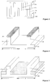
- Figure 1 illustrates a top-view of a portion of the semiconductor structure.
- Figure 1 illustrates a substrate and fins.
- the semiconductor structure may also include other components.
- Figure 2 illustrates a perspective view of region 'B' in Figure 1 .
- a base substrate may be provided.
- the base substrate may include a substrate 100 and a plurality of discrete fins (not illustrated) on the substrate 100.
- the substrate 100 may include a pass gate transistor region 'B' as illustrated in Figure 1 .
- the substrate may provide a platform for subsequently forming the semiconductor structure.
- the base substrate may provide a platform for subsequently forming a SRAM.
- the SRAM may include a fin field effect transistor (FinFET), thus the substrate 100 may also include a pull-down transistor region 'A' as illustrated in Figure 1 , and a pull-up transistor region (not illustrated).
- the pull-up transistor region may include a PMOS region, and the pull-down transistor region and the pass gate transistor region may include NMOS regions.
- the pass gate transistor region may be used to form a pass gate transistor, the pull-down transistor region may be used to form a pull-down transistor, and the pull-up transistor region may be used to form a pull-up transistor.
- the pass gate transistor and the pull-down transistor may be formed on a same, single fin. Therefore, the pass gate transistor region and the pull-down transistor region may be adjacent regions along a length direction of the fin.
- the pass gate transistor region may include a first pass gate transistor region I and a second pass gate transistor region II, adjacent to each other along a direction perpendicular to the length direction of fin.
- the first pass gate transistor region I may be used to form a first pass gate transistor
- the second pass gate transistor region II may be used to form a second pass gate transistor.
- the first pass gate transistor and the second pass gate transistor may form a parallel pass gate transistor.
- Both the first pass gate transistor region I and the second pass gate transistor region II may include NMOS regions.
- a fin may be formed on the substrate 100 in the first pass gate transistor region I, and another fin may be formed on the substrate 100 in the second pass gate transistor region II.
- the fin on the substrate 100 in the pull-up transistor region may be referred to a first fin 110.
- the fin on the substrate 100 in the first pass gate transistor region I may be referred to a second fin 120.
- the fin on the substrate 100 in the second pass gate transistor region II may be referred to a third fin 130.
- the pull-down transistor region may also include a first pull-down transistor region (not illustrated) and a second pull-down transistor region (not illustrated), adjacent to each other along the direction perpendicular to the length direction of the fin.
- the first pull-down transistor region may be used to form a first pull-down transistor
- the second pull-down transistor region may be used to form a second pull-down transistor.
- the first pull-down transistor and the second pull-down transistor may form a parallel pull-down transistor.
- Both the first pull-down transistor region and the second pull-down transistor region may include NMOS regions.
- the second fin 120 may be across the first pass gate transistor region I and the first pull-down transistor region
- the third fin 130 may be across the second pass gate transistor region II and the second pull-down transistor region.
- the substrate 100 may be a silicon substrate.
- the substrate may be made of germanium, silicon germanium, silicon carbide, gallium arsenide, or indium gallium.
- the substrate may also be a silicon on insulator (SOI) substrate, a germanium on insulator (GOI) substrate, a glass substrate, or Group III-V compounds substrates, such as a gallium arsenide (GaAs) substrate, or a gallium nitride (GaN) substrate, etc.
- SOI silicon on insulator
- GOI germanium on insulator
- GaAs gallium arsenide
- GaN gallium nitride
- the fins may be made of the same material as the substrate 100.
- the fins may be made of silicon.
- the first fin 110, the second fin 120, and the third fin 130 may be made of silicon.
- the fins may be made of germanium, silicon germanium, silicon carbide, gallium arsenide, or indium gallium, etc.
- forming the substrate 100 and the fins may include: providing an initial substrate; forming a patterned first hard mask layer 200 on the initial substrate; and etching the initial substrate by using the first hard mask layer 200 as a mask to form the substrate 100 and the fins protruding on the substrate 100.
- the first hard mask layer 200 on the top of the fins may be retained after forming the substrate 100 and the fins.
- the first hard mask layer 200 may be made of silicon nitride.
- the first hard mask layer 200 may be used to define a stop position of a planarization process and to protect the top of the fins when subsequently performing the planarization process.
- an isolation structure may be formed (S102).
- Figure 3 illustrates a corresponding semiconductor structure.
- Figure 3 illustrates a perspective view based on Figure 2 .
- an isolation structure 101 may be formed on the substrate 100 between the adjacent fins.
- the isolation structure 101 may cover portions of sidewalls of the fins, and top of the isolation structure 101 may be lower than top of the fins.
- the isolation structure 101 serving as an isolation structure of the semiconductor structure may be used to isolate adjacent devices.
- the isolation structure 101 may be made of silicon oxide.
- the isolation structure may be made of silicon nitride, or silicon oxynitride, etc.
- a method for forming the isolation structure 101 may include: filling an isolation material on the substrate 100 between the adjacent fins, where top of the isolation material may be above top of the first hard mask layer 200 (illustrated in Figure 2 ); polishing to remove the isolation material above the top of the first hard mask layer 200 to form an isolation film; back-etching portions of a thickness of the isolation film until the top and portions of the sidewalls of the fins are exposed to form the isolation structure 101; and removing the first hard mask layer 200.
- a gate structure may be formed (S103).
- Figure 4 illustrates a corresponding semiconductor structure.
- a gate structure 102 may be formed on each fin, across a length portion of each fin and covering portions of the top and sidewalls of each fin.
- the gate structure 102 may be formed on each fin in the pull-up transistor region (not illustrated), the pass gate transistor region 'B' as illustrated in Figure 1 , and the pull-down transistor region 'A' as illustrated in Figure 1 .
- the gate structure 102 in the pull-up transistor region may be across a length portion of the first fin 110 (illustrated in Figure 1 ), and cover portions of the top and sidewalls of the first fin 110.
- the gate structure 102 in the first pass gate transistor region I and the first pull-down transistor region may be across a length portion of the second fin 120, and cover portions of the top and sidewalls of the second fin 120.
- the gate structure 102 in the second pass gate transistor region II and the second pull-down transistor region may be across a length portion of the third fin 130, and cover portions of the top and sidewalls of the third fin 130.
- a high-K last metal gate last process may be used to form the semiconductor structure, thus the gate structure 102 may be a dummy gate structure.
- the gate structure 102 may occupy a special location for subsequently forming a real gate structure of the semiconductor structure.
- the gate structure 102 may be a single-layer structure, or a stacked structure.
- the gate structure 102 may include a dummy gate layer; or the gate structure 102 may include a dummy oxide layer and a dummy gate layer on the dummy oxide layer.
- the dummy gate layer may be made of polysilicon, silicon oxide, silicon nitride, silicon oxynitride, silicon carbide, silicon carbonitride, silicon carboxynitride, or amorphous carbon, etc.
- the dummy oxide layer may be made of silicon oxide, or silicon oxynitride, etc.
- a method for forming the gate structure 102 may include: forming a dummy gate film on the isolation structure 101, where the dummy gate film may be across a length portion of the fins, and cover portions of the top and sidewalls of the fins; forming a second hard mask layer 210 on the dummy gate film, where the second hard mask layer 210 may define a pattern of the gate structure 102 to be formed; and patterning the dummy gate film by using the second hard mask layer 210 as a mask to form the gate structure 102.
- the gate structure may be the real gate structure of the subsequently formed semiconductor structure.
- the gate structure may include a gate dielectric layer and a gate electrode layer on the gate dielectric layer.
- the gate dielectric layer may be made of silicon oxide, or a high-K gate dielectric material, etc.
- the gate electrode layer may be made of polysilicon or a metal material, including one or more of Ti, Ta, TiN, TaN, TiAl, TiAlN, Cu, Al, W, Ag and Au.
- the second hard mask layer 210 on the top of the gate structure 102 may be retained.
- the second hard mask layer 210 may be made of silicon nitride.
- the second hard mask layer 210 may be used to protect the top of the gate structure 102 during subsequent processes.
- the second hard mask layer may be made of silicon oxynitride, silicon carbide, or boron nitride, etc.
- an N-region mask layer may be formed (S104).
- Figures 5-6 illustrate a corresponding semiconductor structure.
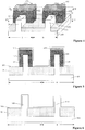
- Figure 5 illustrates a cross-sectional view along a line 'E1E2' on the basis of Figure 4
- Figure 6 illustrates a cross-sectional view along a line 'F1F2' on the basis of Figure 4 .
- an N-region mask layer 300 may be formed on the top and sidewalls of the fins in the pass gate transistor region after forming the gate structure 102 across the length portion of the fins.
- the N-region mask layer 300 may also be formed on top and sidewalls of the gate structure 102 in the pass gate transistor region (illustrated as region 'B' in Figure 1 ) and on the isolation structure 101 in the pass gate transistor region.
- the N-region mask layer 300 may also cover the pull-up transistor region (not illustrated), and the pull-down transistor region 'A' as illustrated in Figure 1 .
- the N-region mask layer 300 may also be on the isolation structure 101 in the pull-up transistor region and the pull-down transistor region.
- the N-region mask layer 300 may be used to protect the sidewalls of the fins from an epitaxial growth process performed on the sidewalls of the first fin 110, the second fin 120 and the third fin 130, when subsequently forming pass gate doped regions by using an epitaxial layer (EPI) process.
- the N-region mask layer 300 may be used as a mask when subsequently forming the pass gate doped regions, such that a distance between the subsequently formed pass gate doped regions and the channel region may increase via the N-region mask layer 300, and the short channel effect may be improved.
- the N-region mask layer 300 may be made of silicon nitride, silicon oxide, boron nitride, or silicon oxynitride, etc.
- the N-region mask layer 300 may be made of a material different from the fins and the isolation structure 101.
- the N-region mask layer 300 may be made of silicon nitride.
- the following method for forming the pass gate doped regions is described herein as an example, although any suitable methods may be included or used for forming the disclosed pass gate doped regions in accordance with various embodiments of the present invention.
- the epitaxial layer process may be first used to form the pass gate doped regions in the second fin 120 on one side of the gate structure 102 in the first pass gate transistor region I (illustrated as region 'C2' in Figure 4 ) and in the third fin 130 on both sides of the gate structure 102 in the second pass gate transistor region II (illustrated as regions 'D1' and 'D2' in Figure 4 ); and then an ion-doped non-epitaxial layer process may be used to form the pass gate doped region in the second fin 120 on the other side of the gate structure 102 in the first pass gate transistor region I (illustrated as region ⁇ C1' in Figure 4 ).
- an N-region trench may be formed (S105).
- Figure 7 illustrates a corresponding semiconductor structure.
- the N-region mask layer 300 on the top of the second fin 120 on one side of the gate structure 102 in the first pass gate transistor region I (illustrated as region 'C2' in Figure 4 ) and on the top of the third fin 130 on both sides of the gate structure 102 in the second pass gate transistor region II (illustrated as regions 'D1' and 'D2' in Figure 4 ) may be etched to expose the top surface of the second fin 120 on one side of the gate structure 102 in the first pass gate transistor region I and the top surface of the third fin 130 on both sides of the gate structure 102 in the second pass gate transistor region II.
- Portions of a thickness of the exposed fins in the first pass gate transistor region I and the second pass gate transistor region II may be etched to form an N-region trench 135 in the second fin 120 on one side of the gate structure 102 in the first pass gate transistor region I and in the third fin 130 on both sides of the gate structure 102 in the second pass gate transistor region II.
- the N-region trench 135 may provide a spatial location for subsequently forming the pass gate doped regions by performing the epitaxial layer process.
- a first patterned layer 220 may be formed to cover the second fin 120 on the other side of the gate structure 102 in the first pass gate transistor region I (illustrated as region 'C1' in Figure 4 ).
- the first patterned layer 220 may cover the N-region mask layer 300 on the other side of the gate structure 102 in the first pass gate transistor region I.
- the first patterned layer 220 may protect the N-region mask layer 300 on the other side of the gate structure 102 in the first pass gate transistor region I.
- the first patterned layer 220 may also cover regions, on one side of the gate structure 102 in the first pass gate transistor region I and in the second pass gate transistor region II, that are not expected to be etched.
- the first patterned layer 220 may be made of a photoresist material. After forming the N-region trench 135, the first patterned layer 220 may be removed by a wet process, or an ashing process, etc.
- a dry etching process may be performed to remove the N-region mask layer 300 on the top of the second fin 120 on one side of the gate structure 102 in the first pass gate transistor region I (illustrated as region 'C2' in Figure 4 ) and on the top of the third fin 130 on both sides of the gate structure 102 in the second pass gate transistor region II (illustrated as regions 'D1' and 'D2' in Figure 4 ).
- the N-region mask layer 300 on the top of the gate structure 102 and on portions of the isolation structure 101 in the first pass gate transistor region I and the second pass gate transistor region II may also be etched when etching the N-region mask layer 300.
- portions of a thickness of the second fin 120 and the third fin 130 may continue to be etched to form the N-region trench 135.
- the N-region mask layer 300 on the sidewalls of the second fin 120 and on the sidewalls of the third fin 130 may also be etched when etching the second fin 120 and the third fin 130. Therefore, after forming the N-region trench 135, the N-region mask layer 300 on the sidewalls of the second fin 120 may be coplanar with the top of the second fin 120, and the N-region mask layer 300 on the sidewalls of the third fin 130 may be coplanar with the top of the third fin 130.
- a cleaning process may be performed on the N-region trench 135.
- the cleaning process may be used not only to remove impurities on the surface of the N- region trench 135, but also to remove an oxide layer (not illustrated) on the surfaces of the second fin 120 and the third fin 130, providing a desired interface state for subsequently forming the pass gate doped regions in the N-region trench 135.
- the cleaning solution used in the cleaning process may be a combination of a mixed solution (SC1 solution), including ammonia, hydrogen peroxide and water, and diluted hydrofluoric acid (DHF), or a combination of ozone water, SC1 solution and DHF.
- SC1 solution mixed solution
- DHF diluted hydrofluoric acid
- epitaxial layer pass gate doped regions on one side of the gate structure in the first pass gate transistor region and in the second pass gate transistor region may be formed (S106).
- Figures 8-9 illustrate a corresponding semiconductor structure.
- Figure 9 illustrates a perspective view of the semiconductor structure (N-region mask layer not illustrated).
- pass gate epitaxial layers 131 may be formed in the N-region trench 135 (illustrated in Figure 7 ), and pass gate doped regions (not illustrated) may be formed in the pass gate epitaxial layers 131.
- the first pass gate transistor region I and the second pass gate transistor region II may include NMOS regions, thus the doped ions in the pass gate doped regions may be N-type ions.
- the pass gate doped region in the first pass gate transistor region I and the pass gate doped regions in the second pass gate transistor region II may be formed in a same, single step.
- the process for forming the pass gate doped regions may include an in-situ doped selective epitaxial process.
- the method for forming the pass gate doped regions in the second fin 120 on one side of the gate structure 102 in the first pass gate transistor region I (illustrated as region 'C2' in Figure 4 ) and in the third fin 130 on both sides of the gate structure 102 in the second pass gate transistor region II (illustrated as regions ⁇ D1' and 'D2' in Figure 4 ) may include: forming the pass gate epitaxial layers 131 in the N-region trench 135, and in-situ self-doping N-type ions during the process for forming the pass gate epitaxial layers 131.
- the pass gate epitaxial layers 131 may be made of Si or SiC, etc.
- the pass gate doped regions may be made of N-type doped Si or SiC, etc.
- the pass gate epitaxial layers 131 may be made of Si, and the N-type ions may be P ions. Therefore, the pass gate doped regions may be made of Si doped with P ions. In other words, the pass gate doped regions may be made of SiP.
- the concentration of the P ions in the pass gate doped regions may be dependent on the process requirements. In one embodiment, the concentration of the P ions in the pass gate doped regions may be in a range of approximately 1 ⁇ 10 20 atoms/cm 3 - 2 ⁇ 10 21 atoms/cm3.
- an N-type ions doping process may be performed on the pass gate epitaxial layers to form the pass gate doped regions.
- the top of the pass gate epitaxial layers 131 may be above the top of the N-region trench 135.
- the top of the pass gate epitaxial layers 131 formed in the N-region trench 135 may be above a top of the fin 120 in the un-etched region ⁇ C1' illustrated in Figure 4 , where the fin 120 has an etched region "C2" to form a portion of the N-region trench 135.
- the sidewall surfaces of the pass gate epitaxial layer 131 above the top of the N-region trench 135 in the first pass gate transistor region I may have a vertex that protrudes away from the second fin 120.
- the sidewall surfaces of the pass gate epitaxial layers 131 above the top of the N-region trench 135 in the second pass gate transistor region II may have a vertex that protrudes away from the third fin 130.
- the top of the pass gate epitaxial layers may be coplanar with the top of the N-region trench.
- a non-epitaxial layer pass gate doped region on the other side of the gate structure in the first pass gate transistor region may be formed (S107).
- Figures 10-11 illustrate a corresponding semiconductor structure.
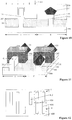
- Figure 10 illustrates a schematic on the basis of Figure 8
- Figure 11 illustrates a perspective view of the semiconductor structure on the basis of Figure 9 (the N-region mask layer and a second patterned layer not illustrated).
- a second patterned layer 230 may be formed to cover the pass gate doped region on one side of the gate structure 102 in the first pass gate transistor region I (illustrated as region 'C2' in Figure 4 ) and the second pass gate transistor region.
- the N-region mask layer 300 on the top of the second fin 120 on the other side of the gate structure 102 in the first pass gate transistor region I may be exposed.
- An ion doping process 125 may be performed on the second fin 120 on the other side of the gate structure 102 in the first pass gate transistor region I by using the second patterned layer 230 as a mask to form a pass gate doped region in the second fin 120 (illustrated as region 'G' in Figure 11 ).
- the second patterned layer 230 may also cover the gate structure 102 and the isolation structure 101 in the first pass gate transistor region I. Further, the second patterned layer 230 may cover regions in the first pass gate transistor region I that are not expected to be exposed.
- the first pass gate transistor region I may include an NMOS region, thus doped ions may be N-type ions during the ion doping process 125 performed on the second fin 120 on the other side of the gate structure 102 in the first pass gate transistor region I.
- the process for forming the pass gate doped region by using the ion doping process 125, the non-epitaxial layer process may include: performing an N-type ions implantation process on the second fin 120 on the other side of the gate structure 102 in the first pass gate transistor region I.
- Parameters of the N-type ions implantation process may be dependent on the process requirements.
- parameters of the N-type ions implantation process may include the following.
- Implanted ions may include P ions and As ions
- an implantation ion energy may be in a range of approximately 1 KeV - 4 KeV
- an implantation dose of the P ions may be in a range of approximately 1 ⁇ 10 15 atoms/cm3 - 2 ⁇ 10 15 atoms/cm 3
- an implantation dose of the As ions may be in a range of approximately 1 ⁇ 10 15 atoms/cm 3 - 4 ⁇ 10 15 atoms/cm3.
- the pass gate doped regions may be formed in the fins on both sides of the gate structure 102 in the pass gate transistor region 'B' as illustrated in Figure 1 . At least one of the pass gate doped regions may be formed by performing an ion-doped non-epitaxial layer process on the fin.
- the method for forming the pass gate doped regions by the epitaxial process may affect the contact resistance between the metal silicide and the pass gate doped region, thus the on-current (I on ) of the formed pass gate transistor may be affected.
- at least one of the pass gate doped regions may be formed by performing an ion-doped non-epitaxial layer process on the fin.
- the epitaxial layer may not be formed in the fin on at least one side of the gate structure 102 in the pass gate transistor region, and an ion implantation process may be performed on the fin on at least one side of the gate structure in the pass gate transistor region.
- the contact resistance between the metal silicide and the pass gate doped region may increase and the on-current (I on ) of the formed pass gate transistor may be reduced.
- the ion-doped non-epitaxial layer process may be performed on the fin on one side of the gate structure 102 in the pass gate transistor region.
- the pass gate doped region 'G' as illustrated in Figure 11 may be formed in the fin on the one side of the gate structure 102 in the pass gate transistor region.
- the process for forming the pass gate doped region in the fin on the other side of the gate structure 102 in the pass gate transistor region may include: forming a pass gate epitaxial layer 131 as illustrated in Figure 9 in the fin on the other side of the gate structure in the pass gate transistor region by performing an epitaxial layer process; and forming the pass gate doped region in the pass gate epitaxial layer 131.
- the pass gate transistor region may include the first pass gate transistor region I and the second pass gate transistor region II, adjacent to each other along the direction perpendicular to the length direction of the fin.
- the pass gate doped regions may be formed in the second fin 120 on both sides of the gate structure 102 in the first pass gate transistor region I and in the third fin 130 on both sides of the gate structure 102 in the second pass gate transistor region II.
- the pass gate transistor region 'G' as illustrated in Figure 11 on one side of the gate structure 102 in the first pass gate transistor region I may be formed by performing the ion doping process 125, the non-epitaxial layer process, on the second fin 120.
- the process for forming the pass gate doped regions in the second fin 120 on other side of the gate structure 102 in the first pass gate transistor region I (illustrated as region 'C2' in Figure 4 ) and in the third fin 130 on both sides of the gate structure 102 in the second pass gate transistor region II (illustrated as regions 'D1' and ⁇ D2' in Figure 4 ) may include: performing the epitaxial layer process on the second fin 120 on other side of the gate structure 102 in the first pass gate transistor region I and on the third fin 130 on both sides of the gate structure 102 in the second pass gate transistor region II to form the pass gate doped regions.
- At least one of the pass gate doped regions may be formed by performing an ion-doped non-epitaxial layer process on the fin.
- the pass gate epitaxial layer may not be formed in the fin on at least one side of the gate structure in the pass gate transistor region.
- the pass gate epitaxial layer may be beneficial for reducing the contact resistance between the subsequently formed metal silicide and the pass gate doped region.
- At least one of the pass gate doped regions may be formed by performing an ion-doped non-epitaxial layer process on the fin, to increase the contact resistance between the subsequently formed metal silicide and the pass gate doped region, such that the on-current (I on ) of the formed pass gate transistor may be reduced.
- the beta ratio of the SRAM is inversely proportional to the magnitude of the on-current (I on ) of the pass gate transistor, the beta ratio of the SRAM in the semiconductor structure consistent with disclosed embodiments may be improved, such that the read margin of the SRAM may be improved, the performance of the SRAM may be improved, and the overall performance of the semiconductor device may be improved.
- a semiconductor structure is also provided in the present invention.
- Figures 12-13 illustrate a semiconductor structure consistent with the disclosed embodiments.
- Figure 12 illustrates a top-view of a portion of the semiconductor structure.
- Figure 1 illustrates a substrate and fins.
- the semiconductor structure may also include other components.
- Figure 13 illustrates a perspective-view of region 'H' in Figure 12 .
- the semiconductor structure may include a base substrate, including a substrate 400 and a plurality of discrete fins (not illustrated) on the substrate 400.
- the substrate 400 may include a pass gate transistor region 'H' as illustrated in Figure 12 .
- the semiconductor structure may also include a gate structure 402, across a length portion of each fin, covering portions of top and sidewalls of each fin, and on each fin.
- the semiconductor structure may include pass gate doped regions (not illustrated) in the fin on both sides of the gate structure 402 in the pass gate transistor region. At least one pass gate doped region on one side of the gate structure may be a non-epitaxial layer doped region in the fin.
- the semiconductor structure on the base substrate may include a SRAM. Therefore, the substrate 400 may also include a pull-down transistor region I as illustrated in Figure 12 and a pull-up transistor region (not illustrated).
- the SRAM may include a FinFET.
- the pull-up transistor region may include a PMOS region, and the pull-down transistor region and the pass gate transistor region may include NMOS regions.
- a pass gate transistor may be formed on the substrate 400 in the pass gate transistor region, a pull-down transistor may be formed on the substrate 400 in the pull-down transistor region, and a pull-up transistor may be formed on the substrate 400 in the pull-up transistor region.
- the pass gate transistor and the pull-down transistor may be formed on a same, single fin. Therefore, the pass gate transistor and the pull-down transistor may be adjacent regions along a length portion of the fin.
- the pass gate transistor region may include a first pass gate transistor region I and a second pass gate transistor region II as illustrated in Figure 13 , adjacent to each other along a direction perpendicular to the length direction of fin.
- a first pass gate transistor may be formed in the first pass gate transistor region I
- a second pass gate transistor may be formed in the second pass gate transistor region II.
- the first pass gate transistor and the second pass gate transistor may form a parallel pass gate transistor.
- Both the first pass gate transistor region I and the second pass gate transistor region II may include NMOS regions.
- a fin may be formed on the substrate 400 in the first pass gate transistor region I, and another fin may be formed on the substrate 400 in the second pass gate transistor region II.
- the fin formed on the substrate 400 in the pull-up transistor region may be referred to a first fin 410.
- the fin formed on the substrate 400 in the first pass gate transistor region I may be referred to a second fin 420.
- the fin formed on the substrate 400 in the second pass gate transistor region II may be referred to a third fin 430.
- the pull-down transistor region may also include a first pull-down transistor region (not illustrated) and a second pull-down transistor region (not illustrated), adjacent to each other along the direction perpendicular to the length direction of the fin.
- a first pull-down transistor may be formed on the substrate 400 in the first pull-down transistor region, and a second pull-down transistor may be formed on the substrate 400 in the second pull-down transistor region.
- the first pull-down transistor and the second pull-down transistor may form a parallel pull-down transistor.
- Both the first pull-down transistor region and the second pull-down transistor region may include NMOS regions.
- the second fin 420 may be across the first pass gate transistor region I and the first pull-down transistor region
- the third fin 430 may be across the second pass gate transistor region II and the second pull-down transistor region.
- the substrate 400 may be a silicon substrate.
- the substrate may be made of germanium, silicon germanium, silicon carbide, gallium arsenide, or indium gallium.
- the substrate may also be a silicon on insulator (SOI) substrate, a germanium on insulator (GOI) substrate, a glass substrate, or Group III-V compounds substrates, such as a gallium arsenide (GaAs) substrate, or a gallium nitride (GaN) substrate, etc.
- SOI silicon on insulator
- GOI germanium on insulator
- GaN gallium nitride
- the fins may be made of the same material as the substrate 400.
- the fins may be made of silicon.
- the first fin 410, the second fin 420, and the third fin 430 may be made of silicon.
- the fins may be made of germanium, silicon germanium, silicon carbide, gallium arsenide, or indium gallium, etc.
- the semiconductor structure may include an isolation structure 401 formed on the substrate 400 between the adjacent fins.
- the isolation structure 401 may cover portions of sidewalls of the fins, and top of the isolation structure 401 may be lower than the top of the fins.
- the isolation structure 401 serving as an isolation structure of the semiconductor structure may be used to isolate adjacent devices.
- the isolation structure 401 may be made of silicon oxide.
- the isolation structure may be made of silicon nitride, or silicon oxynitride, etc.
- the gate structure 402 may be formed on each fin in the pull-up transistor region, the pass gate transistor region, and the pull-down transistor region.
- the gate structure 402 in the pull-up transistor region may be across a length portion of the first fin 410, and cover portions of the top and sidewalls of the first fin 410.
- the gate structure 402 in the first pass gate transistor region I and the first pull-down transistor region (not illustrated) may be across a length portion of the second fin 420, and cover portions of the top and sidewalls of the second fin 420.
- the gate structure 402 in the second pass gate transistor region II and the second pull-down transistor region may be across a length portion of the third fin 430, and cover portions of the top and sidewalls of the third fin 430.
- the gate structure may include a gate dielectric layer and a gate electrode layer on the gate dielectric layer.
- the gate dielectric layer may be made of silicon oxide, or a high-K gate dielectric material, etc.
- the gate electrode layer may be made of polysilicon or a metal material, including one or more of Ti, Ta, TiN, TaN, TiAl, TiAlN, Cu, Al, W, Ag and Au.
- At least one pass gate doped region on one side of the gate structure may be the non-epitaxial layer doped region formed in the fin.
- an epitaxial layer EPI
- EPI epitaxial layer
- the pass gate doped region in the fin on one side of the gate structure 402 in the pass gate transistor region may be the non-epitaxial layer doped region.
- the pass gate doped region in the fin on the other side of the gate structure 402 in the pass gate transistor region may be the non-epitaxial layer doped region.
- the fin on the other side of the gate structure 402 in the pass gate transistor region may include an epitaxial layer.
- the pass gate transistor region may include a first pass gate transistor region I and a second pass gate transistor region II, adjacent to each other along the direction perpendicular to the length direction of fin. Therefore, in one embodiment, the pass gate doped region in the second fin 420 on one side of the gate structure 402 in the first pass gate transistor region I may be the non-epitaxial layer doped region 'J' as illustrated in Figure 13 .
- the pass gate doped regions in the second fin 420 on the other side of the gate structure 402 in the first pass gate transistor region I, and in the third fin 430 on both sides of the gate structure 402 in the second pass gate transistor region II may be the epitaxial layer doped regions.
- pass gate epitaxial layers 431 may be formed in the second fin 420 on the other side of the gate structure 402 in the first pass gate transistor region I, and in the third fin 430 on both sides of the gate structure 402 in the second pass gate transistor region II.
- the pass gate epitaxial layers 431 may be made of Si or SiC, etc.
- the first pass gate transistor region I and the second pass gate transistor region II may include NMOS regions, thus the pass gate doped regions may be doped with N-type ions.
- the pass gate doped region serving as the epitaxial layer doped region may be made of SiP.
- Concentration of the doped ions in the pass gate doped region serving as the epitaxial layer doped region may be dependent on the process requirements.
- the concentration of the P ions in the pass gate doped region may be in a range of approximately 1 ⁇ 1020 atoms/cm 3 - 2 ⁇ 10 21 atoms/cm3.
- doped ions of the pass gate doped region serving as the non-epitaxial layer doped region may include P ions and As ions. Concentration of the doped ions in the pass gate doped region serving as the non-epitaxial layer doped region may be dependent on the process requirements. In one embodiment, the concentration of the P ions in the pass gate doped region may be in a range of approximately 1 ⁇ 10 15 atoms/cm 3 - 2 ⁇ 10 15 atoms/cm 3 , and the concentration of the As ions in the pass gate doped region may be in a range of approximately 1 ⁇ 10 15 atoms/cm 3 - 4 ⁇ 10 15 atoms/cm 3 .
- the semiconductor structure may include the pass gate doped regions in the fin on both sides of the gate structure in the pass gate transistor region, and at least one of the pass gate doped regions in the fin on one side of the gate structure may be the non-epitaxial layer doped region formed in the fin.
- the pass gate epitaxial layer may not be formed in the fin on at least one side of the gate structure in the pass gate transistor region.
- the pass gate epitaxial layer may be beneficial for reducing the contact resistance between the metal silicide and the pass gate doped region in the semiconductor structure.
- At least one of the pass gate doped regions in the fin on one side of the gate structure may be the non-epitaxial layer doped region, thus the contact resistance between the metal silicide and the pass gate doped region may increase, and the on-current of the pass gate transistor may be reduced.
- the beta ratio of the SRAM is inversely proportional to the magnitude of the on-current of the pass gate transistor, the beta ratio of the SRAM in the semiconductor structure consistent with disclosed embodiments may be improved, such that the read margin of the SRAM may be improved, the performance of the SRAM may be improved, and the overall performance of the semiconductor device may be improved.
- a SRAM is also provided in the present invention.
- the SRAM may include a semiconductor structure described herein.
- at least one of the pass gate doped regions in the fin on one side of the gate structure may be a non-epitaxial layer doped region formed in the fin.
- an epitaxial layer may not be formed in the fin on at least one side of the gate structure, thus the on-current of the pass gate transistor in the SRAM may be small.
- the beta ratio of the SRAM is inversely proportional to the magnitude of the on-current of the pass gate transistor, the beta ratio of the SRAM consistent with disclosed embodiments may be improved, such that the read margin of the SRAM may be improved.
Landscapes
- Engineering & Computer Science (AREA)
- Microelectronics & Electronic Packaging (AREA)
- Computer Hardware Design (AREA)
- Semiconductor Memories (AREA)
- Metal-Oxide And Bipolar Metal-Oxide Semiconductor Integrated Circuits (AREA)
- Insulated Gate Type Field-Effect Transistor (AREA)
Applications Claiming Priority (1)
| Application Number | Priority Date | Filing Date | Title |
|---|---|---|---|
| CN201611065220.8A CN108122973B (zh) | 2016-11-28 | 2016-11-28 | 半导体结构及其形成方法、以及sram |
Publications (2)
| Publication Number | Publication Date |
|---|---|
| EP3327776A2 true EP3327776A2 (de) | 2018-05-30 |
| EP3327776A3 EP3327776A3 (de) | 2018-08-22 |
Family
ID=60450434
Family Applications (1)
| Application Number | Title | Priority Date | Filing Date |
|---|---|---|---|
| EP17202701.3A Withdrawn EP3327776A3 (de) | 2016-11-28 | 2017-11-21 | Halbleiterstruktur, statischer direktzugriffsspeicher und herstellungsverfahren dafür |
Country Status (3)
| Country | Link |
|---|---|
| US (2) | US10685965B2 (de) |
| EP (1) | EP3327776A3 (de) |
| CN (1) | CN108122973B (de) |
Families Citing this family (5)
| Publication number | Priority date | Publication date | Assignee | Title |
|---|---|---|---|---|
| CN108122976B (zh) * | 2016-11-29 | 2020-11-03 | 中芯国际集成电路制造(上海)有限公司 | 半导体结构及其形成方法、以及sram |
| CN108695382B (zh) * | 2017-04-07 | 2021-07-06 | 中芯国际集成电路制造(上海)有限公司 | 半导体装置及其制造方法 |
| US11164746B2 (en) * | 2018-06-26 | 2021-11-02 | Taiwan Semiconductor Manufacturing Co., Ltd. | Method of manufacturing semiconductor devices and a semiconductor device |
| CN111128880B (zh) * | 2018-10-31 | 2022-12-02 | 中芯国际集成电路制造(上海)有限公司 | 半导体结构及其形成方法 |
| US11552169B2 (en) * | 2019-03-27 | 2023-01-10 | Intel Corporation | Source or drain structures with phosphorous and arsenic co-dopants |
Family Cites Families (14)
| Publication number | Priority date | Publication date | Assignee | Title |
|---|---|---|---|---|
| KR0136932B1 (ko) * | 1994-07-30 | 1998-04-24 | 문정환 | 반도체 소자 및 그의 제조방법 |
| US6576521B1 (en) | 1998-04-07 | 2003-06-10 | Agere Systems Inc. | Method of forming semiconductor device with LDD structure |
| US7358121B2 (en) * | 2002-08-23 | 2008-04-15 | Intel Corporation | Tri-gate devices and methods of fabrication |
| US7166897B2 (en) * | 2004-08-24 | 2007-01-23 | Freescale Semiconductor, Inc. | Method and apparatus for performance enhancement in an asymmetrical semiconductor device |
| US7449373B2 (en) | 2006-03-31 | 2008-11-11 | Intel Corporation | Method of ion implanting for tri-gate devices |
| US7964465B2 (en) | 2008-04-17 | 2011-06-21 | International Business Machines Corporation | Transistors having asymmetric strained source/drain portions |
| US8283231B2 (en) | 2008-06-11 | 2012-10-09 | Taiwan Semiconductor Manufacturing Company, Ltd. | finFET drive strength modification |
| US8557692B2 (en) | 2010-01-12 | 2013-10-15 | Taiwan Semiconductor Manufacturing Company, Ltd. | FinFET LDD and source drain implant technique |
| US8637930B2 (en) * | 2011-10-13 | 2014-01-28 | International Business Machines Company | FinFET parasitic capacitance reduction using air gap |
| US8664060B2 (en) * | 2012-02-07 | 2014-03-04 | United Microelectronics Corp. | Semiconductor structure and method of fabricating the same |
| CN103515434B (zh) * | 2012-06-26 | 2016-01-06 | 中芯国际集成电路制造(上海)有限公司 | Mos晶体管及其形成方法、sram存储单元电路 |
| US9231106B2 (en) | 2013-03-08 | 2016-01-05 | Taiwan Semiconductor Manufacturing Company, Ltd. | FinFET with an asymmetric source/drain structure and method of making same |
| CN104576536B (zh) | 2013-10-10 | 2017-11-14 | 中芯国际集成电路制造(上海)有限公司 | 一种半导体器件及其制造方法和电子装置 |
| US9391171B2 (en) * | 2014-01-24 | 2016-07-12 | International Business Machines Corporation | Fin field effect transistor including a strained epitaxial semiconductor shell |
-
2016
- 2016-11-28 CN CN201611065220.8A patent/CN108122973B/zh active Active
-
2017
- 2017-11-13 US US15/811,146 patent/US10685965B2/en active Active
- 2017-11-21 EP EP17202701.3A patent/EP3327776A3/de not_active Withdrawn
-
2020
- 2020-05-08 US US16/870,044 patent/US11393829B2/en active Active
Non-Patent Citations (1)
| Title |
|---|
| None |
Also Published As
| Publication number | Publication date |
|---|---|
| CN108122973B (zh) | 2020-06-09 |
| US11393829B2 (en) | 2022-07-19 |
| US20180151572A1 (en) | 2018-05-31 |
| US20200266201A1 (en) | 2020-08-20 |
| EP3327776A3 (de) | 2018-08-22 |
| US10685965B2 (en) | 2020-06-16 |
| CN108122973A (zh) | 2018-06-05 |
Similar Documents
| Publication | Publication Date | Title |
|---|---|---|
| US11393829B2 (en) | Semiconductor structure, static random access memory and fabrication method thereof | |
| US10177146B2 (en) | Semiconductor structure with improved punch-through and fabrication method thereof | |
| EP3327788B1 (de) | Halbleiterstruktur, statischer direktzugriffsspeicher und herstellungsverfahren dafür | |
| US10541238B2 (en) | FinFET and fabrication method thereof | |
| TWI622129B (zh) | 半導體結構及其製造方法 | |
| CN108122852B (zh) | 半导体结构及其形成方法 | |
| EP3331012B1 (de) | Sram-halbleiterbauelemente und herstellungsverfahren dafür | |
| US8952453B2 (en) | MOSFET formed on an SOI wafer with a back gate | |
| US20160126327A1 (en) | Method of making a split gate memory cell | |
| KR20090108917A (ko) | 반도체 소자 및 그 제조 방법 | |
| EP3331005A1 (de) | Sram-vorrichtungen und herstellungsverfahren dafür | |
| CN113327978A (zh) | 半导体结构及其形成方法 | |
| US11094596B2 (en) | Semiconductor structure | |
| US9287130B1 (en) | Method for single fin cuts using selective ion implants | |
| US9224655B2 (en) | Methods of removing gate cap layers in CMOS applications | |
| US20150145046A1 (en) | Semiconductor structure and method for manufacturing the same | |
| US11152370B2 (en) | Memory structure having transistors and capacitor and manufacturing method thereof | |
| CN113690144B (zh) | Mos晶体管及其制造方法与包含mos晶体管的三维存储器 | |
| CN108573873A (zh) | 半导体器件的制造方法 | |
| CN109920733B (zh) | 半导体结构及晶体管的形成方法 | |
| US20250374508A1 (en) | Semiconductor device and method | |
| US20150187910A1 (en) | Methods of manufacturing semiconductor devices and electronic devices | |
| US10727130B2 (en) | Semiconductor device and fabrication method thereof | |
| CN103811316A (zh) | 半导体器件及其制造方法 | |
| CN109309050A (zh) | 半导体结构及其形成方法 |
Legal Events
| Date | Code | Title | Description |
|---|---|---|---|
| PUAI | Public reference made under article 153(3) epc to a published international application that has entered the european phase |
Free format text: ORIGINAL CODE: 0009012 |
|
| STAA | Information on the status of an ep patent application or granted ep patent |
Free format text: STATUS: THE APPLICATION HAS BEEN PUBLISHED |
|
| AK | Designated contracting states |
Kind code of ref document: A2 Designated state(s): AL AT BE BG CH CY CZ DE DK EE ES FI FR GB GR HR HU IE IS IT LI LT LU LV MC MK MT NL NO PL PT RO RS SE SI SK SM TR |
|
| AX | Request for extension of the european patent |
Extension state: BA ME |
|
| PUAL | Search report despatched |
Free format text: ORIGINAL CODE: 0009013 |
|
| AK | Designated contracting states |
Kind code of ref document: A3 Designated state(s): AL AT BE BG CH CY CZ DE DK EE ES FI FR GB GR HR HU IE IS IT LI LT LU LV MC MK MT NL NO PL PT RO RS SE SI SK SM TR |
|
| AX | Request for extension of the european patent |
Extension state: BA ME |
|
| RIC1 | Information provided on ipc code assigned before grant |
Ipc: H01L 29/66 20060101ALI20180716BHEP Ipc: H01L 27/11 20060101AFI20180716BHEP Ipc: H01L 21/8234 20060101ALI20180716BHEP Ipc: H01L 29/78 20060101ALI20180716BHEP |
|
| RAP1 | Party data changed (applicant data changed or rights of an application transferred) |
Owner name: SEMICONDUCTOR MANUFACTURING INTERNATIONAL (BEIJING Owner name: SEMICONDUCTOR MANUFACTURING INTERNATIONAL (SHANGHA |
|
| STAA | Information on the status of an ep patent application or granted ep patent |
Free format text: STATUS: REQUEST FOR EXAMINATION WAS MADE |
|
| 17P | Request for examination filed |
Effective date: 20190207 |
|
| RBV | Designated contracting states (corrected) |
Designated state(s): AL AT BE BG CH CY CZ DE DK EE ES FI FR GB GR HR HU IE IS IT LI LT LU LV MC MK MT NL NO PL PT RO RS SE SI SK SM TR |
|
| STAA | Information on the status of an ep patent application or granted ep patent |
Free format text: STATUS: EXAMINATION IS IN PROGRESS |
|
| 17Q | First examination report despatched |
Effective date: 20210326 |
|
| STAA | Information on the status of an ep patent application or granted ep patent |
Free format text: STATUS: THE APPLICATION IS DEEMED TO BE WITHDRAWN |
|
| 18D | Application deemed to be withdrawn |
Effective date: 20210806 |