EP3331012B1 - Sram-halbleiterbauelemente und herstellungsverfahren dafür - Google Patents
Sram-halbleiterbauelemente und herstellungsverfahren dafür Download PDFInfo
- Publication number
- EP3331012B1 EP3331012B1 EP17204264.0A EP17204264A EP3331012B1 EP 3331012 B1 EP3331012 B1 EP 3331012B1 EP 17204264 A EP17204264 A EP 17204264A EP 3331012 B1 EP3331012 B1 EP 3331012B1
- Authority
- EP
- European Patent Office
- Prior art keywords
- layer
- region
- type
- transistor
- transistor region
- Prior art date
- Legal status (The legal status is an assumption and is not a legal conclusion. Google has not performed a legal analysis and makes no representation as to the accuracy of the status listed.)
- Active
Links
Images


Classifications
-
- H—ELECTRICITY
- H10—SEMICONDUCTOR DEVICES; ELECTRIC SOLID-STATE DEVICES NOT OTHERWISE PROVIDED FOR
- H10B—ELECTRONIC MEMORY DEVICES
- H10B10/00—Static random access memory [SRAM] devices
-
- H—ELECTRICITY
- H10—SEMICONDUCTOR DEVICES; ELECTRIC SOLID-STATE DEVICES NOT OTHERWISE PROVIDED FOR
- H10B—ELECTRONIC MEMORY DEVICES
- H10B10/00—Static random access memory [SRAM] devices
- H10B10/12—Static random access memory [SRAM] devices comprising a MOSFET load element
-
- H—ELECTRICITY
- H10—SEMICONDUCTOR DEVICES; ELECTRIC SOLID-STATE DEVICES NOT OTHERWISE PROVIDED FOR
- H10B—ELECTRONIC MEMORY DEVICES
- H10B10/00—Static random access memory [SRAM] devices
- H10B10/18—Peripheral circuit regions
-
- H—ELECTRICITY
- H10—SEMICONDUCTOR DEVICES; ELECTRIC SOLID-STATE DEVICES NOT OTHERWISE PROVIDED FOR
- H10D—INORGANIC ELECTRIC SEMICONDUCTOR DEVICES
- H10D64/00—Electrodes of devices having potential barriers
- H10D64/01—Manufacture or treatment
- H10D64/013—Manufacture or treatment of electrodes having a conductor capacitively coupled to a semiconductor by an insulator
- H10D64/01302—Manufacture or treatment of electrodes having a conductor capacitively coupled to a semiconductor by an insulator the insulator being formed after the semiconductor body, the semiconductor being silicon
- H10D64/01304—Manufacture or treatment of electrodes having a conductor capacitively coupled to a semiconductor by an insulator the insulator being formed after the semiconductor body, the semiconductor being silicon characterised by the conductor
- H10D64/01316—Manufacture or treatment of electrodes having a conductor capacitively coupled to a semiconductor by an insulator the insulator being formed after the semiconductor body, the semiconductor being silicon characterised by the conductor the conductor comprising a layer of elemental metal contacting the insulator, e.g. Ta, W, Mo or Al
-
- H—ELECTRICITY
- H10—SEMICONDUCTOR DEVICES; ELECTRIC SOLID-STATE DEVICES NOT OTHERWISE PROVIDED FOR
- H10D—INORGANIC ELECTRIC SEMICONDUCTOR DEVICES
- H10D64/00—Electrodes of devices having potential barriers
- H10D64/01—Manufacture or treatment
- H10D64/013—Manufacture or treatment of electrodes having a conductor capacitively coupled to a semiconductor by an insulator
- H10D64/01302—Manufacture or treatment of electrodes having a conductor capacitively coupled to a semiconductor by an insulator the insulator being formed after the semiconductor body, the semiconductor being silicon
- H10D64/01304—Manufacture or treatment of electrodes having a conductor capacitively coupled to a semiconductor by an insulator the insulator being formed after the semiconductor body, the semiconductor being silicon characterised by the conductor
- H10D64/01318—Manufacture or treatment of electrodes having a conductor capacitively coupled to a semiconductor by an insulator the insulator being formed after the semiconductor body, the semiconductor being silicon characterised by the conductor the conductor comprising a layer of alloy material, compound material or organic material contacting the insulator, e.g. TiN
-
- H—ELECTRICITY
- H10—SEMICONDUCTOR DEVICES; ELECTRIC SOLID-STATE DEVICES NOT OTHERWISE PROVIDED FOR
- H10D—INORGANIC ELECTRIC SEMICONDUCTOR DEVICES
- H10D64/00—Electrodes of devices having potential barriers
- H10D64/01—Manufacture or treatment
- H10D64/017—Manufacture or treatment using dummy gates in processes wherein at least parts of the final gates are self-aligned to the dummy gates, i.e. replacement gate processes
-
- H—ELECTRICITY
- H10—SEMICONDUCTOR DEVICES; ELECTRIC SOLID-STATE DEVICES NOT OTHERWISE PROVIDED FOR
- H10D—INORGANIC ELECTRIC SEMICONDUCTOR DEVICES
- H10D64/00—Electrodes of devices having potential barriers
- H10D64/20—Electrodes characterised by their shapes, relative sizes or dispositions
- H10D64/27—Electrodes not carrying the current to be rectified, amplified, oscillated or switched, e.g. gates
- H10D64/311—Gate electrodes for field-effect devices
- H10D64/411—Gate electrodes for field-effect devices for FETs
- H10D64/511—Gate electrodes for field-effect devices for FETs for IGFETs
- H10D64/517—Gate electrodes for field-effect devices for FETs for IGFETs characterised by the conducting layers
-
- H—ELECTRICITY
- H10—SEMICONDUCTOR DEVICES; ELECTRIC SOLID-STATE DEVICES NOT OTHERWISE PROVIDED FOR
- H10D—INORGANIC ELECTRIC SEMICONDUCTOR DEVICES
- H10D64/00—Electrodes of devices having potential barriers
- H10D64/60—Electrodes characterised by their materials
- H10D64/66—Electrodes having a conductor capacitively coupled to a semiconductor by an insulator, e.g. MIS electrodes
- H10D64/665—Electrodes having a conductor capacitively coupled to a semiconductor by an insulator, e.g. MIS electrodes the conductor comprising a layer of elemental metal contacting the insulator, e.g. tungsten or molybdenum
- H10D64/666—Electrodes having a conductor capacitively coupled to a semiconductor by an insulator, e.g. MIS electrodes the conductor comprising a layer of elemental metal contacting the insulator, e.g. tungsten or molybdenum the conductor further comprising additional layers
-
- H—ELECTRICITY
- H10—SEMICONDUCTOR DEVICES; ELECTRIC SOLID-STATE DEVICES NOT OTHERWISE PROVIDED FOR
- H10D—INORGANIC ELECTRIC SEMICONDUCTOR DEVICES
- H10D64/00—Electrodes of devices having potential barriers
- H10D64/60—Electrodes characterised by their materials
- H10D64/66—Electrodes having a conductor capacitively coupled to a semiconductor by an insulator, e.g. MIS electrodes
- H10D64/667—Electrodes having a conductor capacitively coupled to a semiconductor by an insulator, e.g. MIS electrodes the conductor comprising a layer of alloy material, compound material or organic material contacting the insulator, e.g. TiN workfunction layers
-
- H—ELECTRICITY
- H10—SEMICONDUCTOR DEVICES; ELECTRIC SOLID-STATE DEVICES NOT OTHERWISE PROVIDED FOR
- H10D—INORGANIC ELECTRIC SEMICONDUCTOR DEVICES
- H10D84/00—Integrated devices formed in or on semiconductor substrates that comprise only semiconducting layers, e.g. on Si wafers or on GaAs-on-Si wafers
- H10D84/01—Manufacture or treatment
- H10D84/0123—Integrating together multiple components covered by H10D12/00 or H10D30/00, e.g. integrating multiple IGBTs
- H10D84/0126—Integrating together multiple components covered by H10D12/00 or H10D30/00, e.g. integrating multiple IGBTs the components including insulated gates, e.g. IGFETs
- H10D84/0165—Integrating together multiple components covered by H10D12/00 or H10D30/00, e.g. integrating multiple IGBTs the components including insulated gates, e.g. IGFETs the components including complementary IGFETs, e.g. CMOS devices
- H10D84/0172—Manufacturing their gate conductors
- H10D84/0177—Manufacturing their gate conductors the gate conductors having different materials or different implants
-
- H—ELECTRICITY
- H10—SEMICONDUCTOR DEVICES; ELECTRIC SOLID-STATE DEVICES NOT OTHERWISE PROVIDED FOR
- H10D—INORGANIC ELECTRIC SEMICONDUCTOR DEVICES
- H10D84/00—Integrated devices formed in or on semiconductor substrates that comprise only semiconducting layers, e.g. on Si wafers or on GaAs-on-Si wafers
- H10D84/01—Manufacture or treatment
- H10D84/0123—Integrating together multiple components covered by H10D12/00 or H10D30/00, e.g. integrating multiple IGBTs
- H10D84/0126—Integrating together multiple components covered by H10D12/00 or H10D30/00, e.g. integrating multiple IGBTs the components including insulated gates, e.g. IGFETs
- H10D84/0165—Integrating together multiple components covered by H10D12/00 or H10D30/00, e.g. integrating multiple IGBTs the components including insulated gates, e.g. IGFETs the components including complementary IGFETs, e.g. CMOS devices
- H10D84/0172—Manufacturing their gate conductors
- H10D84/0179—Manufacturing their gate conductors the gate conductors having different shapes or dimensions
-
- H—ELECTRICITY
- H10—SEMICONDUCTOR DEVICES; ELECTRIC SOLID-STATE DEVICES NOT OTHERWISE PROVIDED FOR
- H10D—INORGANIC ELECTRIC SEMICONDUCTOR DEVICES
- H10D84/00—Integrated devices formed in or on semiconductor substrates that comprise only semiconducting layers, e.g. on Si wafers or on GaAs-on-Si wafers
- H10D84/01—Manufacture or treatment
- H10D84/0123—Integrating together multiple components covered by H10D12/00 or H10D30/00, e.g. integrating multiple IGBTs
- H10D84/0126—Integrating together multiple components covered by H10D12/00 or H10D30/00, e.g. integrating multiple IGBTs the components including insulated gates, e.g. IGFETs
- H10D84/0165—Integrating together multiple components covered by H10D12/00 or H10D30/00, e.g. integrating multiple IGBTs the components including insulated gates, e.g. IGFETs the components including complementary IGFETs, e.g. CMOS devices
- H10D84/0181—Manufacturing their gate insulating layers
-
- H—ELECTRICITY
- H10—SEMICONDUCTOR DEVICES; ELECTRIC SOLID-STATE DEVICES NOT OTHERWISE PROVIDED FOR
- H10D—INORGANIC ELECTRIC SEMICONDUCTOR DEVICES
- H10D84/00—Integrated devices formed in or on semiconductor substrates that comprise only semiconducting layers, e.g. on Si wafers or on GaAs-on-Si wafers
- H10D84/01—Manufacture or treatment
- H10D84/0123—Integrating together multiple components covered by H10D12/00 or H10D30/00, e.g. integrating multiple IGBTs
- H10D84/0126—Integrating together multiple components covered by H10D12/00 or H10D30/00, e.g. integrating multiple IGBTs the components including insulated gates, e.g. IGFETs
- H10D84/0165—Integrating together multiple components covered by H10D12/00 or H10D30/00, e.g. integrating multiple IGBTs the components including insulated gates, e.g. IGFETs the components including complementary IGFETs, e.g. CMOS devices
- H10D84/0193—Integrating together multiple components covered by H10D12/00 or H10D30/00, e.g. integrating multiple IGBTs the components including insulated gates, e.g. IGFETs the components including complementary IGFETs, e.g. CMOS devices the components including FinFETs
-
- H—ELECTRICITY
- H10—SEMICONDUCTOR DEVICES; ELECTRIC SOLID-STATE DEVICES NOT OTHERWISE PROVIDED FOR
- H10D—INORGANIC ELECTRIC SEMICONDUCTOR DEVICES
- H10D84/00—Integrated devices formed in or on semiconductor substrates that comprise only semiconducting layers, e.g. on Si wafers or on GaAs-on-Si wafers
- H10D84/01—Manufacture or treatment
- H10D84/02—Manufacture or treatment characterised by using material-based technologies
- H10D84/03—Manufacture or treatment characterised by using material-based technologies using Group IV technology, e.g. silicon technology or silicon-carbide [SiC] technology
- H10D84/038—Manufacture or treatment characterised by using material-based technologies using Group IV technology, e.g. silicon technology or silicon-carbide [SiC] technology using silicon technology, e.g. SiGe
-
- H—ELECTRICITY
- H10—SEMICONDUCTOR DEVICES; ELECTRIC SOLID-STATE DEVICES NOT OTHERWISE PROVIDED FOR
- H10D—INORGANIC ELECTRIC SEMICONDUCTOR DEVICES
- H10D84/00—Integrated devices formed in or on semiconductor substrates that comprise only semiconducting layers, e.g. on Si wafers or on GaAs-on-Si wafers
- H10D84/80—Integrated devices formed in or on semiconductor substrates that comprise only semiconducting layers, e.g. on Si wafers or on GaAs-on-Si wafers characterised by the integration of at least one component covered by groups H10D12/00 or H10D30/00, e.g. integration of IGFETs
- H10D84/82—Integrated devices formed in or on semiconductor substrates that comprise only semiconducting layers, e.g. on Si wafers or on GaAs-on-Si wafers characterised by the integration of at least one component covered by groups H10D12/00 or H10D30/00, e.g. integration of IGFETs of only field-effect components
- H10D84/83—Integrated devices formed in or on semiconductor substrates that comprise only semiconducting layers, e.g. on Si wafers or on GaAs-on-Si wafers characterised by the integration of at least one component covered by groups H10D12/00 or H10D30/00, e.g. integration of IGFETs of only field-effect components of only insulated-gate FETs [IGFET]
- H10D84/85—Complementary IGFETs, e.g. CMOS
-
- H—ELECTRICITY
- H10—SEMICONDUCTOR DEVICES; ELECTRIC SOLID-STATE DEVICES NOT OTHERWISE PROVIDED FOR
- H10D—INORGANIC ELECTRIC SEMICONDUCTOR DEVICES
- H10D84/00—Integrated devices formed in or on semiconductor substrates that comprise only semiconducting layers, e.g. on Si wafers or on GaAs-on-Si wafers
- H10D84/80—Integrated devices formed in or on semiconductor substrates that comprise only semiconducting layers, e.g. on Si wafers or on GaAs-on-Si wafers characterised by the integration of at least one component covered by groups H10D12/00 or H10D30/00, e.g. integration of IGFETs
- H10D84/82—Integrated devices formed in or on semiconductor substrates that comprise only semiconducting layers, e.g. on Si wafers or on GaAs-on-Si wafers characterised by the integration of at least one component covered by groups H10D12/00 or H10D30/00, e.g. integration of IGFETs of only field-effect components
- H10D84/83—Integrated devices formed in or on semiconductor substrates that comprise only semiconducting layers, e.g. on Si wafers or on GaAs-on-Si wafers characterised by the integration of at least one component covered by groups H10D12/00 or H10D30/00, e.g. integration of IGFETs of only field-effect components of only insulated-gate FETs [IGFET]
- H10D84/85—Complementary IGFETs, e.g. CMOS
- H10D84/853—Complementary IGFETs, e.g. CMOS comprising FinFETs
-
- H—ELECTRICITY
- H10—SEMICONDUCTOR DEVICES; ELECTRIC SOLID-STATE DEVICES NOT OTHERWISE PROVIDED FOR
- H10D—INORGANIC ELECTRIC SEMICONDUCTOR DEVICES
- H10D84/00—Integrated devices formed in or on semiconductor substrates that comprise only semiconducting layers, e.g. on Si wafers or on GaAs-on-Si wafers
- H10D84/80—Integrated devices formed in or on semiconductor substrates that comprise only semiconducting layers, e.g. on Si wafers or on GaAs-on-Si wafers characterised by the integration of at least one component covered by groups H10D12/00 or H10D30/00, e.g. integration of IGFETs
- H10D84/82—Integrated devices formed in or on semiconductor substrates that comprise only semiconducting layers, e.g. on Si wafers or on GaAs-on-Si wafers characterised by the integration of at least one component covered by groups H10D12/00 or H10D30/00, e.g. integration of IGFETs of only field-effect components
- H10D84/83—Integrated devices formed in or on semiconductor substrates that comprise only semiconducting layers, e.g. on Si wafers or on GaAs-on-Si wafers characterised by the integration of at least one component covered by groups H10D12/00 or H10D30/00, e.g. integration of IGFETs of only field-effect components of only insulated-gate FETs [IGFET]
- H10D84/85—Complementary IGFETs, e.g. CMOS
- H10D84/856—Complementary IGFETs, e.g. CMOS the complementary IGFETs having different architectures than each other, e.g. high-voltage and low-voltage CMOS
Definitions
- the present invention generally relates to the field of semiconductor fabrication technology and, more particularly, relates to semiconductor devices and fabrication methods thereof.
- IC integrated circuit
- memory devices account for a large proportion of the IC products.
- CPU central processing unit
- the memory device may need to be compatible with the embedded CPU platform, and the original specifications and the corresponding electrical performance of the memory device may need to be retained.
- the memory device may need to be compatible with the embedded standard logic device.
- the device may often include a logic region and a storage region.
- the logic region may usually include a plurality of logic devices
- the storage region may include a plurality of memory devices.
- SRAMs static random access memories
- DRAMs dynamic random access memories
- EEPROMs erasable programmable read-only memories
- flash memories etc.
- SRAM devices demonstrate a number of advantages such as low energy-consumption, relatively-fast operation speed, etc. Therefore, SRAM devices and the corresponding fabrication methods have attracted more and more attention.
- Document US 9 502 416 B1 discloses a semiconductor device including transistors having different threshold voltages.
- Said semiconductor device includes first through fourth areas, first through fourth gate stacks, wherein the first gate stack includes a first high-dielectric layer, a first TiN layer to contact the first high-dielectric layer, and a first gate metal on the first TiN layer.
- the second gate stack includes a second high-dielectric layer, a second TiN layer to contact the second high-dielectric layer, and a second gate metal on the second TiN layer.
- the third gate stack includes a third high-dielectric layer, a third TiN layer to contact the third high-dielectric layer, and a third gate metal on the third TiN layer.
- the fourth gate stack includes a fourth high-dielectric layer, a fourth TiN layer to contact the fourth high-dielectric layer, and a fourth gate metal on the fourth TiN layer, the first through fourth thicknesses of the TiN layers being different.
- a first aspect of the present invention provides a method for fabricating a semiconductor device.
- the method includes providing a base substrate including an N-type logic region, a P-type logic region, a first pull down (PD) transistor region, a second PD transistor region, and a pass gate (PG) transistor region.
- the N-type logic region includes a first N-type threshold-voltage (TV) region used to form a first N-type device and a second N-type TV region used to form a second N-type device.
- the P-type logic region includes a first P-type TV region used to form a first P-type device and a second P-type TV region used to form a second P-type device.
- the method also includes forming a gate dielectric layer on a portion of the base substrate in the N-type logic region, the P-type logic region, the first PD transistor region, the second PD transistor region, and the PG transistor region, forming a first work function (WF) layer on the gate dielectric layer in the first N-type TV region, the P-type logic region, the second PD transistor region, and the PG transistor region, forming a second WF layer on the first WF layer in the first P-type TV region, and forming a third WF layer on the second WF layer in the first P-type TV region, the first WF layer in the second P-type TV region, and the gate dielectric layer in the second N-type TV region and the first PD transistor region.
- WF work function
- the thickness of the third WF layer is smaller than the thickness of the first WF layer.
- the method further includes forming a fourth WF layer on the third WF layer in the P-type logic region, the second N-type TV region, and the first PD transistor region, and on the first WF layer in the first N-type TV region, the second PD transistor region, and the PG transistor region.
- the threshold voltage of the first N-type device is larger than the threshold voltage of the second N-type device.
- the threshold voltage of the first P-type device is smaller than the threshold voltage of the second P-type device.
- forming the first WF layer, the second WF layer and the third WF layer includes: forming the first WF layer on the gate dielectric layer; forming the second WF layer on the first WF layer; removing a portion of the second WF layer in the second P-type TV region, the second N-type TV region, and the first PD transistor region; removing a portion of the first WF layer in the second N-type TV region and the first PD transistor region; forming the third WF layer on a remaining portion of the second WF layer, the first WF layer in the second P-type TV region, and the gate dielectric layer in the second N-type TV region and the first PD transistor region; and removing a portion of the third WF layer and the second WF layer in the first N-type TV region, the second PD transistor region, and the PG transistor region.
- forming the first WF layer on the gate dielectric layer includes: forming a first WF material layer on the gate dielectric layer; and forming a second WF material layer on the first WF material layer, wherein: the second WF material layer and the first WF material layer together form the first WF layer, the first WF material layer and the second WF layer are made of a same material, and the second WF material layer and the second WF layer are made of different materials.
- the first WF material layer is made of at least one of Ta, TiN, TaN, TaSiN, and TiSiN.
- the second WF material layer is made of at least one of Ta, TiN, TaN, TaSiN, and TiSiN.
- the second WF layer is made of at least one of Ta, TiN, TaN, TaSiN, and TiSiN.
- the third WF layer is made of at least one of Ta, TiN, TaN, TaSiN, and TiSiN.
- the fourth WF layer is made of at least one of TiAl, TiAlC, TaAl, TaAlC, TiAIN, TaCN, and AlN.
- the first WF material layer, the second WF layer, and the third WF layer are made of TiN.
- the second WF material layer is made of TaN; the thickness of the first WF layer is in a range of approximately 10 ⁇ to 40 ⁇ .
- the thickness of the second WF layer is in a range of approximately 5 ⁇ to 30 ⁇ .
- the thickness of the third WF layer is in a range of approximately 5 ⁇ to 20 ⁇ .
- the thickness of the fourth WF layer is in a range of approximately 40 ⁇ to 60 ⁇ .
- removing the portion of the second WF layer in the second P-type TV region, the second N-type TV region, and the first PD transistor region as well as the portion of the first WF layer in the second N-type VT region and the first PD transistor region includes: removing the second WF layer in the second P-type TV region; and removing both the second WF layer and the first WF layer in the second N-type TV region and the first PD transistor region.
- the method further includes: forming a cap layer on the gate dielectric layer; and forming an etch stop layer on the cap layer, wherein: the cap layer is made of TiN or TiSiN, and the etch stop layer is made of TaN or TaSiN.
- the base substrate also includes a pull up, (PU), transistor region.
- PU pull up,
- the gate dielectric layer is formed in the PU transistor region
- the first WF layer is formed on the gate dielectric layer in the PU transistor region
- the third WF layer is formed on the first WF layer in the PU transistor region.
- the first WF layer in the PU transistor region is formed simultaneously with the first WF layer in the second P-type TV region.
- the third WF layer in the PU transistor region is formed simultaneously with the third WF layer in the second P-type TV region.
- the second N-type TV region includes an N-type ultra-low threshold-voltage(ULTV) region and an N-type low threshold-voltage (LTV) region
- the first N-type TV region is an N-type standard TV region
- the first P-type TV region includes a P-type ULTV region and a P-type LTV region
- the second P-type TV region is a P-type standard TV region.
- the method comprises, prior to forming the gate dielectric layer: a first N-type TV doping adjustment process is performed on the base substrate in the N-type ULTV region; a second N-type TV doping adjustment process is performed on the base substrate in the N-type LTV region; a first P-type TV doping adjustment process is performed on the base substrate in the P-type ULTV region; and a second P-type TV doping adjustment process is performed on the base substrate in the P-type LTV region.
- the method further includes: forming a gate electrode layer on the fourth WF layer.
- the base substrate includes a substrate and a plurality of fin structures formed on the substrate, and the gate dielectric layer is formed across the fin structures and covers a portion of top and sidewall surfaces of the fin structures.
- the PG transistor region includes a first PG transistor region used to form a first PG transistor and a second PG transistor region used to form a second PG transistor.
- a second aspect of the present invention provides a semiconductor device.
- the semiconductor device includes a base substrate including an N-type logic region, a P-type logic region, a first pull down (PD) transistor region, a second PD transistor region, and a pass gate (PG) transistor region.
- the N-type logic region includes a first N-type threshold-voltage (TV) region used to form a first N-type device and a second N-type TV region used to form a second N-type device.
- the P-type logic region includes a first P-type TV region used to form a first P-type device and a second P-type TV region used to form a second P-type device.
- the semiconductor device also includes a gate dielectric layer formed on a portion of the base substrate in the N-type logic region, the P-type logic region, the first PD transistor region, the second PD transistor region, and the PG transistor region, a first WF layer on the gate dielectric layer in the first N-type TV region, the P-type logic region, the second PD transistor region, and the PG transistor region, a second WF layer formed on the first WF layer in the first P-type TV region, and a third WF layer formed on the second WF layer in the first P-type TV region, the first WF layer in the second P-type TV region, and the gate dielectric layer in the second N-type TV region and the first PD transistor region.
- the thickness of the third WF layer is smaller than the thickness of the first WF layer.
- the semiconductor device further includes a fourth WF layer formed on the third WF layer in the P-type logic region, the second N-type TV region, and the first PD transistor region, and on the first WF layer in the first N-type TV region, the second PD transistor region, and the PG transistor region.
- the first WF layer includes a first WF material layer and a second WF material layer formed on the first WF material layer.
- the first WF material layer and the second WF layer are made of a same material.
- the second WF material layer and the second WF layer are made of different materials.
- the first WF material layer is made of at least one of Ta, TiN, TaN, TaSiN, and TiSiN.
- the second WF material layer is made of at least one of Ta, TiN, TaN, TaSiN, and TiSiN.
- the second WF layer is made of at least one of Ta, TiN, TaN, TaSiN, and TiSiN.
- the third WF layer is made of at least one of Ta, TiN, TaN, TaSiN, and TiSiN.
- the fourth WF layer is made of at least one of TiAl, TiAlC, TaAl, TaAlC, TiAlN, TaCN, and AlN.
- the first WF material layer, the second WF layer, and the third WF layer are made of TiN.
- the second WF material layer is made of TaN.
- the thickness of the first WF layer is in a range of approximately 10 ⁇ to 40 ⁇ .
- a thickness of the second WF layer is in a range of approximately 5 ⁇ to 30 ⁇ .
- the thickness of the third WF layer is in a range of approximately 5 ⁇ to 20 ⁇ .
- a thickness of the fourth WF layer is in a range of approximately 40 ⁇ to 60 ⁇ .
- the base substrate also includes a PU transistor region.
- the gate dielectric layer is formed in the PU transistor region
- the first WF layer is formed on the gate dielectric layer in the PU transistor region
- the third WF layer is formed on the first WF layer in the PU transistor region.
- the PG transistor region includes a first PG transistor region and a second PG transistor region; and the first PG transistor region includes a first PG transistor and the second PG transistor region includes a second PG transistor.
- the method further includes: a gate electrode layer formed on the fourth WF layer.
- a semiconductor device according to the second aspect of the present invention may be obtained by a method according to the first aspect of the present invention.
- An SRAM device mainly includes a plurality of pull up (PU) transistors, pull down (PD) transistors, and pass gate (PG) transistors.
- PU pull up
- PD pull down
- PG pass gate
- the read margin of a memory device is proportional to the beta ratio of the memory device.
- the beta ratio refers to the ratio of the open-state current of the PD transistor to the open-state current of the PG transistor.
- the memory unit includes a PU transistor, two PD transistors, and two PG transistors.
- the work function (WF) layers in the two PD transistors are identical with the WF layer in an N-type standard threshold-voltage (TV) logic device and the WF layers in the two PG transistors are identical with the WF layer in an N-type low TV logic device.
- the beta ratio of the memory device may be improved.
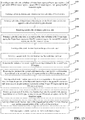
- FIG. 13 illustrates a flowchart of an exemplary method for fabricating a semiconductor device consistent with various disclosed embodiments in the present invention.
- FIGS. 1-12 illustrate schematic views of semiconductor structures at certain stages of the exemplary fabrication process.
- FIG. 1 shows a schematic cross-section view of a corresponding semiconductor structure.
- the base substrate may include an N-type logic region (not labeled), a P-type logic region (not labeled), a first PD transistor region II1, a second PD transistor region II2, and a PG transistor region (not labeled).
- the N-type logic region may include a first N-type TV region 41 used to form a first N-type device, and a second N-type TV region 42 used to form a second N-type device.
- the threshold voltage of the first N-type device may be larger than the threshold voltage of the second N-type device.
- the P-type logic region may include a first P-type TV region 31 used to form a first P-type device, and a second P-type TV region 32 used to form a second P-type device.
- the threshold voltage of the first P-type device may be smaller than the threshold voltage of the second P-type device.
- the semiconductor device to be formed includes a logic device and an SRAM device.
- the N-type logic region may provide a process platform for subsequent formation of an N-type device
- the P-type logic region may provide a process platform for subsequent formation of a P-type device
- the first PD transistor region II1 may provide a process platform for subsequent formation of a first PD transistor
- the second PD transistor region II2 may provide a process platform for subsequent formation of a second PD transistor
- the PG transistor region may provide a process platform for subsequent formation of PG transistors.
- the first PD transistor and the second PD transistor may together serve as PD transistors of the SRAM in the semiconductor device.
- the first PD transistor region II1 may be an N-type metal-oxide-semiconductor (NMOS) region
- the second PD transistor region II2 may be an NMOS region
- the PG transistor region may also be an NMOS region.
- the base substrate may include a PU transistor region I, the PU transistor region I may provide a process platform for subsequent formation of PU transistors.
- the PU transistor region I may be a P-type metal-oxide-semiconductor (PMOS) region.
- PMOS P-type metal-oxide-semiconductor
- the PG transistor region may further include a first PG transistor region III1 and a second PG transistor region III2 adjacent to the first PG transistor region III1.
- the first PG transistor region III1 may provide a process platform for subsequent formation of a first PG transistor and the second PG transistor region III2 may provide a process platform for subsequent formation of a second PG transistor.
- the first PG transistor and the second PG transistor may together serve as PG transistors of the SRAM in the semiconductor device.
- the first PG transistor region III1 and the second PG transistor region III2 may both be NMOS regions.
- the first N-type TV region 41 may be an N-type standard TV region
- the second N-type TV region 42 may include an N-type ultra-low threshold-voltage (ULTV) region and an N-type low TV region.
- the second N-type TV region may include only an N-type low TV region.
- the first P-type TV region 31 may include a P-type ULTV region and a P-type low TV region
- the second P-type TV region 32 may be a P-type standard TV region.
- the first P-type TV region may only include a P-type low TV region.
- the semiconductor device to be formed is described to be a fin field-effect transistor (Fin-FET) device, although any suitable transistors may be encompassed within the scope of present invention.
- the base substrate may include a substrate 101 and a plurality of discrete fin structures 102 formed on the substrate 101.
- the base substrate may also include an isolation structure 114 formed on the portion of the substrate 101 exposed by the plurality of fin structures 102.
- the isolation structure 114 may cover a portion of the sidewall surfaces of each fin structure 102 and the top surface of the isolation structure 114 may be lower than the top surfaces of the fin structures 102.
- the isolation structure 114 may be made of SiO x , SiN x , SiON, or any other appropriate material. In one embodiment, the isolation structure 114 is made of SiO x .
- the semiconductor device to be formed may be a planar transistor device.
- the base substrate may be a planar base substrate.
- the planar base substrate may be made of silicon, germanium, SiGe, SiC, silicon on insulator (SOI), germanium on insulator (GOI), glass, III-V group compound (such as GaN, GaAs, etc.), or any other appropriate semiconductor material or structure.
- SOI silicon on insulator
- GOI germanium on insulator
- III-V group compound such as GaN, GaAs, etc.
- a plurality of the gate structures may be formed on the surface of the planar substrate.
- the substrate 101 may be made of silicon, germanium, SiGe, SiC, GaAs, InAs, or any other appropriate semiconductor material.
- the substrate 101 may also be made SOI or GOI.
- the plurality of fin structures 102 may be made of silicon, germanium, SiGe, SiC, GaAs, InAs, or any other appropriate semiconductor material.
- the substrate 101 is made of silicon and the fin structures 102 is also made of silicon.
- the fabrication process may include performing a first N-type TV doping adjustment process on the portion of the base substrate corresponding to the N-type ULTV region, performing a second N-type TV doping adjustment process on the portion of the base substrate corresponding to the N-type low TV region, performing a first P-type TV doping adjustment process on the portion of the base substrate corresponding to the P-type ULTV region, and performing a second P-type TV doping adjustment process on the portion of the base substrate corresponding to the P-type low TV region.
- the doping ions used in the first N-type TV doping adjustment process and the second N-type TV doping adjustment process may be N-type ions, including P ions, As ions, Sb ions, etc.
- the doping concentration introduced in the first N-type TV doping adjustment process may be lower than the doping concentration introduced in the second N-type TV doping adjustment process.
- the doping ions used in the first P-type TV doping adjustment process and the second P-type doping adjustment process may be P-type ions, including B ions, Ga ions, In ions, etc.
- the doping concentration introduced in the first P-type TV doping adjustment process may be lower than the doping concentration introduced in the second P-type TV doping adjustment process.
- FIG. 2 shows a schematic cross-section view of a corresponding semiconductor structure.
- a high-k last metal last process may be adopted to form a plurality of gate structures. Therefore, the fabrication process may include forming a plurality of dummy gate structures 120 on the portion of the base substrate in the N-type logic region, the P-type logic region, the first PD transistor region II1, the second PD transistor region II2, and the PG transistor region.
- a plurality of dummy gate structures 120 may be formed on the base substrate across the plurality of fin structures 102.
- the plurality of dummy gate structures 120 may be used to occupy spaces for a plurality of subsequently-formed gate structures of the semiconductor device.
- the plurality of dummy gate structures 120 may be formed on the isolation structure 114 across the plurality of fin structures 102.
- the dummy gate structures 120 may cover a portion of the top and the sidewall surfaces of each fin structure 102.
- the dummy gate structure 102 may have a single-layer structure or a multiple-layer structure.
- the dummy gate structure 102 may include a dummy gate layer or may include a dummy oxide layer and a dummy gate layer formed on the dummy oxide layer.
- the dummy gate layer may be made of poly-crystalline silicon, SiO x , SiN x , SiON, SiC, SiCN, SiCON, or amorphous silicon.
- the dummy oxide layer may be made of SiO x or SiON.
- the dummy gate structure 120 may also be formed on the portion of the base substrate in the PU transistor region I.
- the dummy gate structure 120 may be formed across the N-type logic region, the P-type logic region, the first PD transistor region II1, the second PD transistor region II2, the PG transistor region, and the PU transistor region I.
- the dummy gate structures formed in different regions of the base substrate may be independent from each other. That is, the dummy gate structures formed in different regions of the base substrate may not be connected with each other.
- a plurality of doped source/drain regions may be formed (S403). Specifically, after forming the dummy gate structures 120, the plurality of doped source/drain regions (not shown) may be formed in each fin structure 102 on the two opposite sides of the corresponding dummy gate structure 120.
- FIG. 3 shows a schematic cross-section view of a corresponding semiconductor structure. It may be noted that FIG. 3 illustrates a cross-section view in a direction perpendicular to a length direction of the fin structure 102, while, along the length direction of the fin structure 102, doped source/drain regions (not illustrated) may be formed in the each fin structure 102 on the two opposite sides of the removed corresponding dummy gate structure 120.
- the plurality of dummy gate structures 120 may be removed.
- the plurality of dummy gate structures 120 may be removed by a dry etching process, a wet etching process, or a SiCoNi etching process.
- the fabrication process may include forming an interlayer dielectric layer (not shown) on the portion of the base substrate exposed by the dummy gate structures 120.
- the interlayer dielectric layer may expose the top surfaces of the plurality of dummy gate structures 120. That is, the interlayer dielectric layer may not cover the top surfaces of the plurality of dummy gate structures 120.
- a gate dielectric layer may be formed on a portion of the base substrate in the N-type logic region, the P-type logic region, the first PD transistor region, the second PD transistor region, and the PG transistor region (S405).
- FIG. 4 shows a schematic cross-section view of a corresponding semiconductor structure.
- a gate dielectric layer 204 may be formed on a portion of the base substrate in the N-type logic region, the P-type logic region, the first PD transistor region II1, the second PD transistor region II2, and the PG transistor region.
- the base substrate may also include a PU transistor region I, and accordingly, during the fabrication process for the gate dielectric layer 204, the gate dielectric layer 204 may also be formed on the portion of the base substrate in the PU transistor region I.
- the gate dielectric layer 204 may include an interfacial layer (not shown) and a high-k dielectric layer (not shown) formed on the interfacial layer. Specifically, during the fabrication of the gate dielectric layer 204, the gate dielectric layer 204 may be formed across the fin structures 102 to cover a portion of the top and the sidewall surfaces of each fin structure 102.
- the interfacial layer may provide a desired interfacial basis for the formation of the high-k dielectric layer so that the quality of the formed high-k dielectric layer may be improved. As such, the density of interface states between the high-k dielectric layer and the fin structures 102 may be reduced, avoiding undesired effects due to direct contact between the high-k dielectric layer and the fin structures 102.
- the interfacial layer may be made of SiO x or SiON.
- the interfacial layer may be formed by an oxidation process. Moreover, the interfacial layer may be only formed on the portion of the top and the sidewall surfaces exposed by the plurality of fin structures 102. In other embodiments, the interfacial layer may be made by a deposition process, such as chemical vapor deposition (CVD), physical vapor deposition (PVD), and atomic layer deposition (ALD). The interfacial layer may also be formed on the isolation structure.
- CVD chemical vapor deposition
- PVD physical vapor deposition
- ALD atomic layer deposition
- the high-k dielectric layer may be a dielectric material with a relative dielectric constant greater than the relative dielectric constant of SiO x .
- the high-k dielectric material used is HfO 2 .
- the high-k dielectric layer may include HfSiO, HfSiON, HfTaO, HfTiO, HfZrO, ZrO 2 , and Al 2 O 3 .
- the high-k dielectric layer may be formed by a CVD, PVD, or ALD process. In one embodiment, the high-k dielectric layer is formed through an ALD process.
- a WF layer may be formed on the gate dielectric layer 204.
- the fabrication process may also include forming a cap layer (not shown) on the gate dielectric layer 204, and then forming an etch stop layer (not shown) on the cap layer.
- the cap layer may provide protection for the gate dielectric layer 204, preventing undesired etching damage to the gate dielectric layer 204 during the subsequent etching process.
- the cap layer may also help prevent the metal ions in a subsequently-formed gate electrode layer from diffusing into the gate dielectric layer 204.
- the cap layer is made of TiN.
- the cap layer may be formed by an ALD process such that the formed cap layer may demonstrate desired step coverage capability.
- the cap layer may be formed by TiSiN, and the cap layer may be formed by a CVD process or a PVD process.
- the etch stop layer may be made of a material different from the material used to subsequently form the WF layer. Therefore, during a subsequent etching process performed to etch the WF layer, the etch rate on the etch stop layer may be relatively small, and thus the etch stop layer may serve as a layer to indicate that the etching process performed on the WF layer needs to be stopped. As such etching damages to the gate dielectric layer 204 may be avoided.
- the etch stop layer is made of TaN.
- the etch stop layer is formed by an ALD process such that the formed etch stop layer may demonstrate desired stop coverage capability.
- the etch stop layer may be made of TaSiN, and the etch stop layer may be formed by a CVD process or a PVD process.
- the subsequent fabrication process may include forming a WF layer on the gate dielectric layer 204 in each region of the semiconductor device corresponding to the device region.
- a WF layer on the gate dielectric layer 204 in each region of the semiconductor device corresponding to the device region.
- the first N-type TV region 41 is used to form a first N-type device
- the second N-type TV region 42 is used to form a second N-type device
- the threshold voltage of the first N-type device is larger than the threshold voltage of the second N-type TV device. Therefore, during the subsequent fabrication process, the WF layers in the first PD transistor region II1 and the second N-type TV region 42 may be formed by a same process and the WF layers in the second PD transistor region II2 and the first N-type TV region 41 may be formed by a same process.
- the disclosed fabrication method may reduce the thickness of the WF layer in the second PD transistor region II2, and thus reduce the overall threshold voltage of the PD transistor region.
- the open-state current of the subsequently-formed PD transistor region may increase, improving the beta ratio and the read margin of the formed memory.
- the WF layer in the PG transistor region and the WF layer in the first N-type TV may be formed by a same process.
- the disclosed fabrication method may improve the thickness of the WF layer in the PG transistor region, and thus improve the effective WF value of the WF layer formed in the PG transistor region. Therefore, the disclosed fabrication method may reduce the open-state current of the subsequently-formed PG transistor, and thus improve the beta ratio and the read margin of the formed memory.
- the threshold voltage of the PG transistor may be improved, the leak current in the semiconductor device may be effectively suppressed.
- the first PG transistor region III1, the second PG transistor region III2, and the first N-type TV region 41 may be formed through a same process.
- a first WF layer may be subsequently formed on the gate dielectric layer 204 in the PU transistor region I and a second WF layer may then be formed on the first WF layer.
- the subsequent process to form the first WF layer and the third WF layer in the PU transistor region I may be the same as the subsequent process to form the first WF layer and the third WF layer in the second P-type TV region.
- the disclosed fabrication method may reduce the thickness of the WF layer in the PU transistor region I, and thus may increase the effective WF value of the WF layer in the PU transistor region.
- the threshold voltage of the formed PU transistor may increase, and the open-state current of the formed PU transistor may be reduced. Therefore, the disclosed fabrication method may be conducive to improving the gamma ratio, and thus may improve the write margin of the formed memory.
- a first work function layer may be formed on the surface of the gate dielectric layer (S406).
- FIG. 5 shows a schematic cross section view of a corresponding semiconductor structure.
- a first WF layer (not shown) may be formed on the gate dielectric layer 204.
- the first WF layer may be formed in the PU transistor region I, the P-type logic region, the N-type logic region, the first PD transistor region II1, the second PD transistor region II2, the first PG transistor region III1, and the second PG transistor region III2.
- the first WF layer may be made of a P-type WF material.
- the P-type WF material may have a WF value in a range of 5.1 eV to 5.5 eV, such as 5.2 eV, 5.3 eV, 5.4 eV, etc.
- the first WF layer may be made of one or more of Ta, TiN, TaN, TaSiN, and TiSiN.
- the first WF layer may be formed by a CVD, PVD, ALD, or any other appropriate disposition process.
- forming the first WF layer on the gate dielectric layer may include forming a first WF material layer 205 on the gate dielectric layer 204 and then forming a second WF material layer 206 on the first WF material layer 205.
- the first WF material layer 205 and the subsequently-formed second WF layer may be made of a same material, and the second WF material layer 206 may be made of a material different from the material used to form the second WF layer.
- the first WF material layer 205 may be made of TiN, and the second WF material layer 206 may be made of TaN.
- the thickness of the first WF layer may be determined based on the threshold voltages of the transistors in the first N-type TV region 41, the second PD transistor region II2, and the PG transistor region. In one embodiment, the thickness of the first WF layer may be in a range of approximately 10 ⁇ to 40 ⁇ .
- FIG. 6 shows a schematic cross-section view of a corresponding semiconductor structure.
- a second WF layer 207 may be formed on the first WF layer.
- the second WF layer 207 may serve as a portion of the WF layer in the first P-type TV region 31 to improve the threshold voltage of the transistors formed in the first P-type TV region 31.
- the second WF layer 207 may be made of a P-type WF material.
- the second WF layer 207 may be made of one or more of Ta, TiN, TaN, TaSiN, and TiSiN.
- the thickness of the second WF layer 207 may be determined based on the threshold voltages of the transistors in the first P-type TV region 31.
- the second WF layer 207 is made of TiN, and the thickness of the second WF layer 207 may be in a range of approximately 5 ⁇ to 30 ⁇ .
- subsequent fabrication process may include removing the portion of the second WF layer 207 formed in the second P-type TV region 32, the second N-type TV region 42, and the first PD transistor region II1. Moreover, the portion of the first WF layer formed in the second N-type TV region 42 and the first PD transistor region II1 may be removed.
- the threshold voltage of the first P-type device formed in the first P-type TV region 31 may be smaller than the threshold voltage of the second P-type device formed in the second P-type TV region 32. Therefore, in one embodiment, by removing the portion of the second WF layer 207 formed in regions other than the first P-type TV region 31, a desired process basis may be provided for subsequent formation of a WF layer with a relatively large thickness on the first P-type TV region 31.
- FIG. 7 shows a schematic cross-section view of a corresponding semiconductor structure.
- the portion of the second WF layer 207 formed in the second P-type TV region 32 may be removed.
- the portion of the second WF layer 207 formed in the PU transistor region I may also be removed.
- the portion of the first WF layer formed in the second P-type TV region 32, and the PU transistor region I may be exposed. Because the second WF material layer 206 and the second WF layer 207 may be made of different materials, undesired etching damages to the first WF layer may be avoided.
- the process to remove the portion of the second WF layer 207 may include the following steps. First, a first patterned layer may be formed on the first P-type TV region 31, the N-type logic region, the first PD transistor region II1, the second transistor region II2, and the PG transistor region. The first patterned layer may expose the portion of the second WF layer 207 formed in the second P-type TV region 32 and the PU transistor region I. Further, the exposed portion of the second WF layer 207 may be removed through etching using the first patterned layer as an etch mask. Moreover, the first patterned layer may then be removed.
- FIG. 8 shows a schematic cross-section view of a corresponding semiconductor structure.
- the portion of second WF layer 207 and the first WF layer formed in the second N-type TV region 42 and the first PD transistor region II1 may be removed.
- the process to remove the portion of the second WF layer 207 and the first WF layer may include the following steps. First, a second patterned layer may be formed on the second WF layer 207 and the exposed portion of the first WF layer. The second patterned layer may expose the portion of the second WF layer 207 formed in the second N-type TV region 42 and the first PD transistor region II1. The exposed portion of the second WF layer 207 and the portion of the first WF layer under the exposed portion of the second WF layer 207 may then be removed through etching using the second patterned layer as an etch mask. Moreover, the second patterned layer may be removed.
- the portion of the second WF layer formed in the second P-type TV region, the second N-type TV region, and the first PD transistor region may be removed first, and the portion of the first WF layer formed in the second N-type TV region and the PD transistor region may then be removed.
- a third work function layer may be formed on the remaining portion of the second work function layer, the portion of the first work function layer in the second P-type TV region, the portion of the gate dielectric layer 204 in the second N-type TV region and the first PD transistor region (S410).
- FIG. 9 shows a schematic cross-section view of a corresponding semiconductor structure.
- a third WF layer 208 may be formed on the remaining portion of the second WF layer 207, the portion of the first WF layer in the second P-type TV region 32, the portion of the gate dielectric layer 204 in the second N-type TV region 42 and the first PD transistor region II1.
- the thickness of the third WF layer 208 may be smaller than the thickness of the first WF layer.
- the third WF layer 208 may serve as a portion of the WF layers in the P-type device, the first PD transistor device, and the second N-type device that are formed subsequently. Because the thickness of the third WF layer 208 is smaller than the thickness of the first WF layer, the thickness of the WF layer formed in the N-type logic region 42 may be smaller than the thickness of the WF layer formed in the first N-type logic region 41. Therefore, the threshold voltage of the second N-type device formed in the second N-type logic device 42 may be smaller than the threshold voltage of the first N-type device formed in the first N-type logic region 41.
- the thickness of the WF layer formed in the first PD transistor region II1 may be smaller than the thickness of the WF layer formed in the second PD transistor region II2 such that the threshold voltage of the first PD transistor may be smaller than the threshold voltage of the second PD transistor.
- the thickness of the WF layer in the first PD transistor region II1 and the thickness of the WF layer in the second N-type logic region 41 may both be relatively small such that the threshold voltage of the first PD transistor may be small. Therefore, the open-state current of the first PD transistor may increase, and thus the read margin of the memory may be improved.
- the third WF layer 208 may be made of a P-type WF material.
- the third WF layer 208 may be made of one or more of Ta, TiN, TaN, TiSiN, etc.
- the thickness of the third WF layer 208 may be determined by the threshold voltage of the transistors formed in the second N-type logic region 42 and the first PD transistor region II1.
- the third WF layer may be made of TiN, and the thickness of the third WF layer may be in a range of approximately 5 ⁇ to 20 ⁇ .
- FIG. 10 shows a schematic cross-section view of a corresponding semiconductor structure.
- the portion of the third WF layer 208 and the second WF layer 207 formed in the first N-type TV region 41, the second PD transistor region II2, and the PG transistor region may be removed.
- the process to remove the portion of the third WF layer 208 and the second WF layer 207 may include the following steps. First, a third patterned layer may be formed on the third WF layer 208. The third patterned layer may expose a portion of the third WF layer 208 formed in the first N-type TV region 41, the second PD transistor region II2, and the PG transistor region. The exposed portion of the third WF layer 208 and the portion of the second WF layer 207 under the exposed portion of the third WF layer 208may be removed through etching using the third patterned layer as an etch mask. Further, the third patterned layer may be removed.
- the remaining portion of the third WF layer 208 may serve as a portion of the WF layers in the P-type logic region, the PU transistor region I, the second N-type TV region 42, and the first PD transistor region II1.
- a fourth work function layer may be formed on the exposed portion of the first work function layer as well as the exposed portion of the third work function layer (S412).
- a fourth WF layer 209 may be formed on the portion of the first WF layer in the first N-type TV region 41, the second PD transistor region II2, and the PG transistor region.
- the fourth WF layer may also be formed on the portion of the third WF layer 208 in the P-type logic region, the PU transistor region I, the second N-type TV region 42, and the first PD transistor region II1.
- the fourth WF layer 209 may sever as a portion of the WF layers in the N-type logic region, the PG transistor region, the first PD transistor region II1, and the second PD transistor region II2.
- the fourth WF layer 209 may be used to adjust the threshold voltages for the first N-type device, the second N-type device, the PG transistor, the first PD transistor, and the second PD transistor that are formed subsequently.
- the portion of the fourth WF layer 209 formed in the P-type logic region and the PU transistor region I may be retained.
- the fourth WF layer 209 may be made of an N-type WF material.
- the N-type WF material may have a WF value in a range of approximately 3.9 eV to 4.5 eV, such as 4 eV, 4.1 eV, 4.3 eV, etc.
- the fourth WF layer 209 may be made of one or more of TiAl, TiAlC, TaAlN, TiAlN, TaCN, AlN, etc.
- the fourth WF layer 209 may be formed by a CVD, PVD, ALD, or any other appropriate deposition process. In one embodiment, the fourth WF layer 209 is made of TiAl.
- the thickness of the fourth WF layer 209 may be determined based on the thickness of the third WF layer 208 and the thickness of the first WF layer, as well as the threshold voltages of the first N-type device, the second N-type device, the first PD transistor, the second PD transistor, and the PG transistor that are formed subsequently. In one embodiment, the thickness of the fourth WF layer 209 is in a range of approximately 40 ⁇ to 60 ⁇ .
- first WF layer and the fourth WF layer 209 in the first N-type TV region 41 may be used to form the WF layer in the first N-type device
- first WF layer and the fourth WF layer 209 in the second PD transistor region II2 may be used to form the WF layer in the second PD transistor
- first WF layer and the fourth WF layer 209 in the PG transistor region may be used to form the WF layer in the PG transistor.
- the first WF layer, the second WF layer 207, and the third WF layer 208 in the first P-type TV region 31 may be used to form the WF layer in the first P-type device
- the first WF layer and the third WF layer 208 in the second P-type TV region 32 may be used to form the WF layer in the second P-type device
- the first WF layer and the third WF layer 208 in the PU transistor region I may be used to form the WF layer in the PU transistor.
- the third WF layer 208 and the fourth WF layer 209 in the second N-type TV region 42 may be used to form the WF layer in the second N-type device, and the third WF layer 208 and the fourth WF layer 209 in the first PD transistor region II1 may be used to form the WF layer in the first PD transistor.
- FIG. 12 shows a schematic cross-section view of a corresponding semiconductor structure.
- the fabrication method may further include forming a gate electrode layer 211 on the fourth WF layer.
- the gate electrode layer 211 may be formed across the N-type logic region, the P-type logic region, the first PD transistor region II1, the second PD transistor region II2, the PU transistor region I, and the PG transistor region.
- the gate electrode layer in each region may be isolated from each other.
- the gate electrode layer 211 may be made of one or more of Al, Cu, Ag, Au, Pt, Ni, Ti, W, etc.
- the gate electrode layer 211 may be formed by a process including the following steps. First, a gate electrode film may be formed on the fourth WF layer 209. The top surface of the gate electrode film may be higher than the top surface of the interlayer dielectric layer (not shown). Further, the portion of the gate electrode film formed above the top surface of interlayer dielectric layer may be removed through polishing to form the gate electrode layer 211.
- the WF layer in the first PD transistor region and the WF layer in the second N-type TV region may be formed by a same process, and the WF layer in the second PD transistor region and the WF layer in the first N-type TV region may be formed by a same process.
- the threshold voltage of the N-type device in the second N-type TV region may be smaller than the threshold voltage of the N-type device in the first N-type TV region.
- the WF layers in the first PD transistor region and the second PD transistor region and the WF layer in the first N-type TV region are formed by a same process.
- the threshold voltage of the PD transistor fabricated by the disclosed methods may be smaller.
- the open-state current of the PD transistors may increase, the beta ratio of the memory in the semiconductor device may be improved, and the read margin may also be improved.
- the fabrication process for the WF layer in the PG transistor region may be the same as the fabrication process for the WF layer in the first N-type TV region.
- the WF layer in the PG transistor region and the WF layer in the second N-type TV region are formed by a same process. Therefore, compared to the threshold voltage of the PG transistor fabricated by conventional methods, the threshold voltage of the PG transistor region fabricated by the disclosed methods may be larger. As such, the open-state current of the PG transistor may be reduced, the beta ratio of the memory in the semiconductor device may be improved, and the read margin may also be improved.
- the present invention also provides a semiconductor device including a logic device and an SRAM device.
- FIG. 12 illustrates a schematic cross-section view of a semiconductor device consistent with various embodiments of the present invention.
- the semiconductor device may include a base substrate.
- the base substrate may include an N-type logic region, a P-type logic region, a first PD transistor region II1, a second PD transistor region II2, and a PG transistor region.
- the N-type logic region may include a first N-type TV region 41 including a first N-type device, and a second N-type TV region 42 including a second N-type device.
- the threshold voltage of the first N-type device may be larger than the threshold voltage of the second N-type device.
- the P-type logic region may include a first P-type TV region 31 including a first P-type device, and a second P-type TV region 32 including a second P-type device.
- the threshold voltage of the first P-type device may be smaller than the threshold voltage of the second P-type device.
- the semiconductor device may also include a gate dielectric layer 204 formed on a portion of the base substrate in the N-type logic region, the P-type logic region, the first PD transistor region II1, the second PD transistor region II2, and the PG transistor, a first WF layer formed on the gate dielectric layer 204 in the P-type logic region, the first N-type TV region 41, the second PD transistor region II2, and the PG transistor region, a second WF layer 207 formed on the first WF layer in the first P-type TV region 31, and a third WF layer 208 formed on the gate dielectric layer 204 in the second N-type TV region 42 and the first PD transistor region II1, the second WF layer 207 in the first P-type TV region 31, and the first WF layer in the second P-type TV region 32.
- the thickness of the third WF layer 208 may be smaller than the thickness of the first WF layer.
- the semiconductor device may further include a fourth WF layer 209 formed on the first WF layer in the first N-type TV region 41, the second PD transistor region II2, and the PG transistor region.
- the fourth WF layer 209 may also be formed on the third WF layer 208 in the P-type logic region, the second N-type TV region 42, and the first PD transistor region
- the base substrate of the semiconductor device may also include a PU transistor region I.
- the PU transistor region I may be a PMOS region.
- the gate dielectric layer 204 may also be formed on the substrate in the PU transistor region I.
- the first WF layer may be formed on the gate dielectric layer 204 in the PU transistor region I
- the third WF layer 208 may be formed on the first WF layer in the PU transistor region I.
- the fourth WF layer 209 may also be formed on the third WF layer 208 in the PU transistor region I.
- the PG transistor region may include a first PG transistor region III1 and a second PG transistor region III2. Further, a first PG transistor may be formed in the first PG transistor region III1, and a second PG transistor may be formed in the second PG transistor region III2.
- the semiconductor device is a Fin-FET device.
- the base substrate may include a substrate 101 and a plurality of discrete fin structures 102 formed on the substrate 101.
- the base substrate may also include an isolation structure 114 formed on the portion of the substrate 101 exposed by the plurality of fin structures 102.
- the isolation structure 114 may cover a portion of the sidewall surfaces of each fin structure 102 and the top surface of the isolation structure 114 may be lower than the top surfaces of the fin structures 102.
- the detailed descriptions of the base substrate and the gate dielectric layer 204 may refer to the above illustration of the disclosed fabrication methods.
- the first WF layer may include a first WF material layer 205 and a second WF material layer 206 formed on the first WF material layer 205.
- the first WF material layer 205 and the second WF layer 207 may be made of a same material, and the second WF material layer 206 may be made of a material different from the material used to form the second WF layer 207.
- the first WF material layer 205 may be made of one or more of Ta, TiN, TaN, TaSiN, and TiSiN.
- the second WF material layer 206 may be made of one or more of Ta, TiN, TaN, TaSiN, and TiSiN.
- the second WF layer 207 may be made of one or more of Ta, TiN, TaN, TaSiN, and TiSiN.
- the third WF layer 208 may be made of one or more of Ta, TiN, TaN, TaSiN, and TiSiN.
- the first WF material layer 205, the second WF layer 207, and the third WF layer 208 are made of TiN, and the second WF material layer 206 is made of TaN.
- the thickness of the first WF layer is in a range of approximately 10 ⁇ to 40 ⁇
- the thickness of the second WF layer 207 is in a range of approximately 5 ⁇ to 30 ⁇
- the thickness of the third WF layer 208 is in a range of approximately 5 ⁇ to 20 ⁇ .
- the fourth WF layer 209 may be made of TiAl, TiAlC, TaAl, TaAlC, TiAlN, TaCN, or AlN. In one embodiment, the fourth WF layer 209 is made of TiAl.
- the semiconductor device may also include a gate electrode layer 211 formed on the fourth WF layer 209.
- the corresponding WF layer when the corresponding WF layer becomes thicker, the effective WF value of the NMOS device is larger, and the corresponding threshold voltage of the NMOS device is also larger.
- the corresponding WF layer may have a multiple-layer structure formed by the first WF layer and the fourth WF layer 209.
- the corresponding WF layer may have a multiple-layer structure formed by the third WF layer 208 and the fourth WF layer 209.
- the effective WF value of the first N-type device, the second PD transistor, and the PG transistor may be larger than the effective WF value of the second N-type device and the first PD transistor. Therefore, the threshold voltage of the first PD transistor may be relatively small such that the open-state current of the PD transistor formed by the first PD transistor and the second PD transistor may increase. Moreover, the threshold voltage of the PG transistor may become relatively large such that the open-state current of the PG transistor may be reduced. As such, the beta ratio of the disclosed semiconductor device may increase, the read margin of the semiconductor device may be improved, and the electrical performance of the semiconductor device may also be improved.
- the WF layer in the PU transistor region is the same as the WF layer of the second P-type device in the second P-type TV region. Therefore, the thickness of the WF layer in the PU transistor region is relatively small such that the effective WF value of the PU transistor may be relatively large. Accordingly, the threshold voltage of the PU transistor may be improved, and the open-state current of the PU transistor may be reduced. As such, the gamma ratio of the semiconductor device may be improved, and thus the write margin of the semiconductor device may be improved.
- the disclosed fabrication methods and semiconductor devices may demonstrate several advantages.
- a first PD transistor, a second PD transistor, and a PG transistor may also be formed.
- the threshold voltage of the first N-type device may be larger than the threshold voltage of the second N-type device.
- the thickness of the WF layer of the first N-type device may be larger than the thickness of the WF layer of the second N-type device.
- the WF layer of the first PD transistor and the WF layer of the second N-type device may be formed by a same process
- the WF layer of the second PD transistor and the WF layer of the first N-type device may be formed by a same process
- the WF layer of the PG transistor and the WF layer of the first N-type device may also be formed by a same process. Therefore, the threshold voltage of the second PD transistor may be smaller than the threshold voltage of the first PD transistor. According to conventional fabrication methods and semiconductor devices, the threshold voltage of the second PD transistor is the same as the threshold voltage of the first PD transistor.
- the open-state current of the PD transistors formed by the first PD transistor and the second PD transistor in the disclosed semiconductor devices may be increased.
- the threshold voltage of the PG transistor in the disclosed semiconductor devices may be larger, which further leads to a smaller open-state current of the PG transistor.
- the disclosed fabrication methods and the semiconductor devices may improve the beta ratio of the memories in the formed semiconductor device, improve the read margin of the memories, and optimize the electrical performance of the semiconductor device.
- the base substrate of the semiconductor devices may also include a PU transistor region.
- the gate dielectric layer, the first WF layer, and the third WF layer may be formed in the PU transistor region.
- the process to form the first WF layer and the third WF layer in the PU transistor region may be the same as the process to form the first WF layer and the third WF layer in the second P-type TV region such that the effective WF value of the WF layer in the PU transistor region may be improved. Therefore, the threshold voltage of the PU transistor may be improved, and thus the open-state current of the PU transistor may be reduced.
- the disclosed fabrication methods and the semiconductor devices may improve the gamma ratio of the memories, and thus improve the write margin of the memories.
Landscapes
- Metal-Oxide And Bipolar Metal-Oxide Semiconductor Integrated Circuits (AREA)
- Chemical & Material Sciences (AREA)
- Composite Materials (AREA)
- Engineering & Computer Science (AREA)
- Materials Engineering (AREA)
Claims (15)
- Verfahren zum Herstellen einer Halbleitervorrichtung, die eine Logikvorrichtung und eine SRAM-Vorrichtung aufweist, wobei das Verfahren aufweist:Bereitstellen eines Basissubstrats einschließlich einer N-Typ-Logikregion, einer P-Typ-Logikregion, einer ersten Pull-Down-, PD-, Transistorregion, einer zweiten PD-Transistorregion, und einem Pass-Gate-, PG-, Transistorregion, wobei die N-Typ-Logikregion aufweist eine erste N-Typ-Schwellenspannungs-, TV-, Region, die verwendet wird, um eine erste N-Typ-Vorrichtung zu bilden, und eine zweite N-Typ-TV-Region (42), die verwendet wird, um eine zweite N-Typ-Vorrichtung zu bilden, wobei die P-Typ-Logikregion aufweist eine erste P-Typ-TV-Region (31), die verwendet wird, um eine erste P-Typ-Vorrichtung zu bilden, und eine zweite P-Typ-TV-Region (32), die verwendet wird, um eine zweite P-Typ-Vorrichtung zu bilden;Bilden einer Gate-Dielektrikumschicht (204) auf einem Teil des Basissubstrats in der N-Typ-Logikregion, der P-Typ-Logikregion, der ersten PD-Transistorregion, der zweiten PD-Transistorregion und der PG-Transistorregion;Bilden einer ersten Arbeitsfunktions-, WF-, Schicht auf der Gate-Dielektrikumschicht (204) in der ersten N-Typ-TV-Region (41), der P-Typ-Logikregion, der zweiten PD-Transistorregion und der PG-Transistorregion;Bilden einer zweiten WF-Schicht (207) auf der ersten WF-Schicht in der ersten P-Typ-TV-Region (31);Bilden einer dritten WF-Schicht (208) auf der zweiten WF-Schicht (207) in der ersten P-Typ-TV-Region (31), der ersten WF-Schicht in der zweiten P-Typ-TV-Region (32) und der Gate- Dielektrikumschicht (204) in der zweiten N-Typ-TV-Region (42) und der ersten PD-Transistorregion, wobei eine Dicke der dritten WF-Schicht (208) kleiner ist als eine Dicke der ersten WF-Schicht; undBilden einer vierten WF-Schicht (209) auf der dritten WF-Schicht (208) in der P-Typ-Logikregion, der zweiten N-Typ-TV-Region (42) und der ersten PD-Transistorregion, und auf der ersten WF-Schicht in der ersten N-Typ-TV-Region (41); der zweiten PD-Transistorregion und der PG-Transistorregion.
- Verfahren gemäß Anspruch 1, wobei:eine Schwellspannung der ersten N-Typ-Vorrichtung größer ist als eine Schwellspannung der zweiten N-Typ-Vorrichtung; undeine Schwellspannung der ersten P-Typ-Vorrichtung kleiner ist als eine Schwellspannung der zweiten P-Typ-Vorrichtung.
- Verfahren gemäß einem der Ansprüche 1 oder 2, wobei Bilden der ersten WF-Schicht, der zweiten WF-Schicht (207) und der dritten WF-Schicht (208) aufweist:Bilden der ersten WF-Schicht auf der Gate- Dielektrikumschicht (204);Bilden der zweiten WF-Schicht (207) auf der ersten WF-Schicht;Entfernen eines Teils der zweiten WF-Schicht (207) in der zweiten P-Typ-TV-Region (32), der zweiten N-Typ-TV-Region (42) und der ersten PD-Transistorregion;Entfernen eines Teils der ersten WF-Schicht in der zweiten N-Typ-TV-Region (42) und der ersten PD-Transistorregion;Bilden der dritten WF-Schicht (208) auf einem verbleibenden Teil der zweiten WF-Schicht (207), der ersten WF-Schicht in der zweiten P-Typ-TV-Region (32), und der Gate-Dielektrikumschicht (204) in der zweiten N-Typ-TV-Region (42) und der ersten PD-Transistorregion; undEntfernen eines Teils der dritten WF-Schicht (208) und der zweiten WF-Schicht (207) in der ersten N-Typ-TV-Region (41), der zweiten PD-Transistorregion und der PG-Transistorregion.
- Verfahren gemäß Anspruch 3, wobei Bilden der ersten WF-Schicht auf der Gate-Dielektrikumschicht (204) aufweist:Bilden einer ersten WF-Materialschicht (205) auf der Gate- Dielektrikumschicht (204); undBilden einer zweiten WF-Materialschicht (206) auf der ersten WF-Materialschicht (205), wobei:die zweite WF-Materialschicht (206) und die ersten WF-Materialschicht (205) zusammen die erste WF-Schicht bilden,die erste WF-Materialschicht (205) und die zweite WF-Schicht (207) aus demselben Material hergestellt sind, unddie zweite WF-Materialschicht (206) und die zweite WF-Schicht (207) aus unterschiedlichen Materialien hergestellt sind; undwobei:die erste WF-Materialschicht (205) hergestellt ist aus wenigstens einem von Ta, TiN, TaN, TaSiN und TiSiN;die zweite WF-Materialschicht (206) hergestellt ist aus wenigstens einem von Ta, TiN, TaN, TaSiN und TiSiN;die zweite WF-Schicht (207) hergestellt ist aus wenigstens einem von Ta, TiN, TaN, TaSiN und TiSiN;die dritte WF-Schicht (208) hergestellt ist aus wenigstens einem von Ta, TiN, TaN, TaSiN und TiSiN; unddie vierte WF-Schicht (209) hergestellt ist aus wenigstens einem von TiAl, TiAlC, TaAl, TaAlC, TiAlN, TaCN und AlN.
- Verfahren gemäß Anspruch 4, wobei:(a) die erste WF-Materialschicht (205), die zweite WF-Schicht (207), und die dritte WF-Schicht (208) hergestellt sind aus TiN; die zweite WF-Materialschicht (206) hergestellt ist aus TaN; die Dicke der ersten WF-Schicht in einem Bereich von 10 Å bis 40 Å liegt; eine Dicke der zweiten WF-Schicht in einem Bereich von 5 Å bis 30 Å liegt; die Dicke der dritten WF-Schicht (208) in einem Bereich von 5 Å bis 20 Å liegt; und eine Dicke der vierten WF-Schicht (209) in einem Bereich von 40 Å bis 60 Å liegt; und/oder(b) Entfernen des Teils der zweiten WF-Schicht (207) in der zweiten P-Typ-TV-Region (32), der zweiten N-Typ-TV-Region (42) und der ersten PD-Transistorregion sowie des Teils der ersten WF-Schicht in der zweiten N-Typ-VT-Region und der ersten PD-Transistorregion aufweist: Entfernen der zweiten WF-Schicht (207) in der zweiten P-Typ-TV-Region (32); und Entfernen sowohl der zweiten WF-Schicht (207) als auch der ersten WF-Schicht in der zweiten N-Typ-TV-Region (42) und der ersten PD-Transistorregion.
- Verfahren gemäß einem der Ansprüche 1 bis 5, nach Bilden der Gate-Dielektrikumschicht (204) und vor Bilden der ersten WF-Schicht weiter aufweisend:Bilden einer Deckschicht auf der Gate- Dielektrikumschicht (204); undBilden einer Ätzstoppschicht auf der Deckschicht, wobei:die Deckschicht hergestellt ist aus TiN oder TiSiN, unddie Ätzstoppschicht hergestellt ist aus TaN oder TaSiN.
- Verfahren gemäß einem der Ansprüche 1 bis 6, wobei:das Basissubstrat außerdem aufweist eine Pull-Up-, PU-, Transistorregion;die Gate-Dielektrikumschicht (204) in der PU-Transistorregion gebildet ist, die erste WF-Schicht auf der Gate-Dielektrikumschicht (204) in der PU-Transistorregion gebildet ist, und die dritte WF-Schicht (208) auf der ersten WF-Schicht in der PU-Transistorregion gebildet ist;die erste WF-Schicht in der PU-Transistorregion gleichzeitig mit der ersten WF-Schicht in der zweiten P-Typ-TV-Region (32) gebildet ist; unddie dritte WF-Schicht (208) in der PU-Transistorregion gleichzeitig mit der dritten WF-Schicht (208) in der zweiten P-Typ-TV-Region (32) gebildet ist.
- Verfahren gemäß einem der Ansprüche 1 bis 7, wobei die zweite N-Typ-TV-Region (42) aufweist eine N-Typ-Ultraniedrig-Schwellspannungs-, ULTV-, Region und eine N-Typ-Niedrigschwellspannungs-, LTV-, Region, wobei die erste N-Typ-TV-Region (41) eine N-Typ-Standard-TV-Region ist, die erste P-Typ-TV-Region (31) aufweist eine P-Typ-ULTV-Region und eine P-Typ-LTV-Region und die zweite P-Typ-TV-Region (32) eine P-Typ-Standard-TV-Region ist, und
wobei, vor Bilden der Gate-Dielektrikumschicht (204):ein erster N-Typ-TV-Dotierungseinstellungsvorgang auf dem Basissubstrat in der N-Typ-ULTV-Region durchgeführt wird;ein zweiter N-Typ-TV-Dotierungseinstellungsvorgang durchgeführt wird auf dem Basissubstrat in der N-Typ-LTV-Region;ein erster P-Typ-TV-Dotierungseinstellungsvorgang durchgeführt wird auf dem Basissubstrat in der P-Typ-ULTV-Region; undein zweiter P-Typ-TV-Dotierungseinstellungsvorgang durchgeführt wird auf dem Basissubstrat in der P-Typ-LTV-Region. - Verfahren gemäß einem der Ansprüche 1 bis 8, nach Bilden der vierten WF-Schicht (209), weiter aufweisend:
Bilden einer Gate-Elektrodenschicht (211) auf der vierten WF-Schicht (209). - Verfahren gemäß einem der Ansprüche 1 bis 9, wobei:(a) das Basissubstrat aufweist ein Substrat (101) und eine Vielzahl von Rippenstrukturen (102), die auf dem Substrat (101) gebildet sind; und die Gate-Dielektrikumschicht (204) über den Rippenstrukturen (102) gebildet ist und einen Teil von Top- und Seitenwandoberflächen der Rippenstrukturen (102) abdeckt; und/oder(b) die PG-Transistorregion aufweist eine erste PG-Transistorregion, die verwendet wurde, um einen ersten PG-Transistor zu bilden, und eine zweite PG-Transistorregion, die verwendet wurde, um einen zweiten PG-Transistor zu bilden.
- Halbleitervorrichtung, die eine Logikvorrichtung und eine SRAM-Vorrichtung aufweist, wobei die Halbleitervorrichtung aufweist:ein Basissubstrat einschließlich einer N-Typ-Logikregion, einer P-Typ-Logikregion, einer ersten Pull-Down-, PD-, Transistorregion, einer zweiten PD-Transistorregion, und einer Pass-Gate-, PG-, Transistorregion, wobei die N-Typ-Logikregion aufweist eine erste N-Typ-Schwellspannungs-, TV-, Region, die verwendet wurde, um eine erste N-Typ-Vorrichtung zu bilden, und eine zweite N-Typ-TV-Region (42), die verwendet wurde, um eine zweite N-Typ-Vorrichtung zu bilden, wobei die P-Typ-Logikregion aufweist eine erste P-Typ-TV-Region (31), die verwendet wurde, um eine erste P-Typ-Vorrichtung zu bilden, und eine zweite P-Typ-TV-Region (32), die verwendet wurde, um eine zweite P-Typ-Vorrichtung zu bilden;eine Gate-Dielektrikumschicht (204), die gebildet ist auf einem Teil des Basissubstrats in der N-Typ-Logikregion, der P-Typ-Logikregion, der ersten PD-Transistorregion, der zweiten PD-Transistorregion und der PG-Transistorregion;einer ersten Arbeitsfunktions-, WF-, Schicht auf der Gate-Dielektrikumschicht (204) in der ersten N-Typ-TV-Region (41), der P-Typ-Logikregion, der zweiten PD-Transistorregion und der PG-Transistorregion;einer zweiten WF-Schicht (207), die gebildet ist auf der ersten WF-Schicht in der ersten P-Typ-TV-Region (31);einer dritten WF-Schicht (208), die gebildet ist auf der zweiten WF-Schicht (207) in der ersten P-Typ-TV-Region (31), der ersten WF-Schicht in der zweiten P-Typ-TV-Region (32) und der Gate-Dielektrikumschicht (204) in der zweiten N-Typ-TV-Region (42) und der ersten PD-Transistorregion, wobei eine Dicke der dritten WF-Schicht (208) kleiner ist als eine Dicke der ersten WF-Schicht; undeiner vierten WF-Schicht (209), die gebildet ist auf der dritten WF-Schicht (208) in der P-Typ-Logikregion, der zweiten N-Typ-TV-Region (42), und der ersten PD-Transistorregion, und auf der ersten WF-Schicht in der ersten N-Typ-TV-Region (31), der zweiten PD-Transistorregion und der PG-Transistorregion.
- Halbleitervorrichtung gemäß Anspruch 11, wobei:die erste WF-Schicht eine erste WF-Materialschicht (205) und eine zweite WF-Materialschicht (206) aufweist, die auf der ersten WF-Materialschicht (205) gebildet ist;die erste WF-Materialschicht (205) und die zweite WF-Schicht (207) aus einem gleichen Material hergestellt sind; unddie zweite WF-Materialschicht (206) und die zweite WF-Schicht (207) aus unterschiedlichen Materialien hergestellt sind.
- Halbleitervorrichtung gemäß Anspruch 12, wobei:die erste WF-Materialschicht (205) hergestellt ist aus wenigstens einem von Ta, TiN, TaN, TaSiN und TiSiN;die zweite WF-Materialschicht (206) hergestellt ist aus wenigstens einem von Ta, TiN, TaN, TaSiN und TiSiN;die zweite WF-Schicht (207) hergestellt ist aus wenigstens einem von Ta, TiN, TaN, TaSiN und TiSiN;die dritte WF-Schicht (208) hergestellt ist aus wenigstens einem von Ta, TiN, TaN, TaSiN TiSiN; unddie vierte WF-Schicht (209) hergestellt ist aus wenigstens einem von TiAl, TiAlC, TaAl, TaAlC, TiAlN, TaCN und AlN; undwobei:die erste WF-Materialschicht (205), die zweite WF-Schicht (207) und die dritte WF-Schicht (208) hergestellt sind aus TiN;die zweite WF-Materialschicht (206) hergestellt ist aus TaN;die Dicke der ersten WF-Schicht in einem Bereich von 10 Å bis 40 Å liegt;eine Dicke der zweiten WF-Schicht (207) in einem Bereich von 5 Å bis 30 Å liegt;die Dicke der dritten WF-Schicht (208) in einem Bereich von 5 Å bis 20 Ä liegt; undeine Dicke der vierten WF-Schicht (209) in einem Bereich von 40 Å bis 60 Å liegt.
- Halbleitervorrichtung gemäß einem der Ansprüche 11 bis 13, wobei:das Basissubstrat außerdem aufweist eine PU-Transistorregion; unddie Gate-Dielektrikumschicht (204) in der PU-Transistorregion gebildet ist, die erste WF-Schicht auf der Gate-Dielektrikumschicht (204) in der PU-Transistorregion gebildet ist, und die dritte WF-Schicht (208) auf der ersten WF-Schicht in der PU-Transistorregion gebildet ist.
- Halbleitervorrichtung gemäß einem der Ansprüche 11 bis 14, wobei:(a) die PG-Transistorregion eine erste PG-Transistorregion und eine zweite PG-Transistorregion aufweist; und die erste PG-Transistorregion einen ersten PG-Transistor aufweist und die zweite PG-Transistorregion einen zweiten PG-Transistor aufweist; und/oder(b) die Halbleitervorrichtung weiter eine Gate-Elektrodenschicht (211) aufweist, die auf der vierten WF-Schicht (209) gebildet ist.
Applications Claiming Priority (1)
| Application Number | Priority Date | Filing Date | Title |
|---|---|---|---|
| CN201611082506.7A CN108122913B (zh) | 2016-11-30 | 2016-11-30 | 半导体器件及其形成方法 |
Publications (2)
| Publication Number | Publication Date |
|---|---|
| EP3331012A1 EP3331012A1 (de) | 2018-06-06 |
| EP3331012B1 true EP3331012B1 (de) | 2019-09-04 |
Family
ID=60515178
Family Applications (1)
| Application Number | Title | Priority Date | Filing Date |
|---|---|---|---|
| EP17204264.0A Active EP3331012B1 (de) | 2016-11-30 | 2017-11-29 | Sram-halbleiterbauelemente und herstellungsverfahren dafür |
Country Status (3)
| Country | Link |
|---|---|
| US (1) | US10199382B2 (de) |
| EP (1) | EP3331012B1 (de) |
| CN (1) | CN108122913B (de) |
Families Citing this family (13)
| Publication number | Priority date | Publication date | Assignee | Title |
|---|---|---|---|---|
| CN108122852B (zh) * | 2016-11-28 | 2019-11-01 | 中芯国际集成电路制造(上海)有限公司 | 半导体结构及其形成方法 |
| US10644134B2 (en) | 2017-05-31 | 2020-05-05 | Taiwan Semiconductor Manufacturing Company, Ltd. | Gate formation with varying work function layers |
| US11114347B2 (en) * | 2017-06-30 | 2021-09-07 | Taiwan Semiconductor Manufacturing Co., Ltd. | Self-protective layer formed on high-k dielectric layers with different materials |
| KR102271008B1 (ko) * | 2017-10-27 | 2021-06-29 | 삼성전자주식회사 | 반도체 장치 |
| KR20250070116A (ko) * | 2017-11-30 | 2025-05-20 | 인텔 코포레이션 | 진보된 집적 회로 구조체 제조를 위한 핀 패터닝 |
| US11329042B2 (en) | 2018-11-30 | 2022-05-10 | Taiwan Semiconductor Manufacturing Co., Ltd. | Gate structures having neutral zones to minimize metal gate boundary effects and methods of fabricating thereof |
| TWI727505B (zh) * | 2018-11-30 | 2021-05-11 | 台灣積體電路製造股份有限公司 | 積體電路裝置及其製造方法 |
| KR102873062B1 (ko) | 2019-03-25 | 2025-10-16 | 삼성전자주식회사 | 집적회로 장치 및 그 제조 방법 |
| US11264289B2 (en) * | 2019-07-11 | 2022-03-01 | Tokyo Electron Limited | Method for threshold voltage tuning through selective deposition of high-K metal gate (HKMG) film stacks |
| US11417653B2 (en) * | 2019-09-30 | 2022-08-16 | Taiwan Semiconductor Manufacturing Company Ltd. | Semiconductor structure and method for forming the same |
| CN113097136B (zh) * | 2020-01-08 | 2024-11-22 | 中芯国际集成电路制造(上海)有限公司 | 半导体结构的形成方法 |
| US11502081B2 (en) * | 2021-01-14 | 2022-11-15 | Taiwan Semiconductor Manufacturing Co., Ltd. | Semiconductor device and method |
| CN113724753B (zh) * | 2021-08-12 | 2025-03-14 | 上海华力集成电路制造有限公司 | 双端口sram的存储单元 |
Family Cites Families (11)
| Publication number | Priority date | Publication date | Assignee | Title |
|---|---|---|---|---|
| US7087977B2 (en) * | 2002-09-27 | 2006-08-08 | Renesas Technology Corp. | Semiconductor device including multiple wiring layers and circuits operating in different frequency bands |
| US7732872B2 (en) * | 2007-10-25 | 2010-06-08 | International Business Machines Corporation | Integration scheme for multiple metal gate work function structures |
| US7911008B2 (en) * | 2007-10-25 | 2011-03-22 | International Business Machines Corporation | SRAM cell having a rectangular combined active area for planar pass gate and planar pull-down NFETS |
| US8406039B2 (en) | 2009-07-13 | 2013-03-26 | Taiwan Semiconductor Manufacturing Company, Ltd. | Low-leakage power supply architecture for an SRAM array |
| US8942030B2 (en) * | 2010-06-25 | 2015-01-27 | Taiwan Semiconductor Manufacturing Company, Ltd. | Structure and method for SRAM cell circuit |
| US9496143B2 (en) * | 2012-11-06 | 2016-11-15 | Globalfoundries Inc. | Metal gate structure for midgap semiconductor device and method of making same |
| KR102056582B1 (ko) * | 2013-06-05 | 2020-01-22 | 삼성전자 주식회사 | 반도체 장치 및 그 제조 방법 |
| KR102290685B1 (ko) * | 2015-06-04 | 2021-08-17 | 삼성전자주식회사 | 반도체 장치 |
| US9640540B1 (en) * | 2016-07-19 | 2017-05-02 | Taiwan Semiconductor Manufacturing Co., Ltd. | Structure and method for an SRAM circuit |
| CN108122852B (zh) * | 2016-11-28 | 2019-11-01 | 中芯国际集成电路制造(上海)有限公司 | 半导体结构及其形成方法 |
| CN108122914B (zh) * | 2016-11-30 | 2019-11-01 | 中芯国际集成电路制造(上海)有限公司 | Sram器件及其制造方法 |
-
2016
- 2016-11-30 CN CN201611082506.7A patent/CN108122913B/zh active Active
-
2017
- 2017-11-22 US US15/821,422 patent/US10199382B2/en active Active
- 2017-11-29 EP EP17204264.0A patent/EP3331012B1/de active Active
Non-Patent Citations (1)
| Title |
|---|
| None * |
Also Published As
| Publication number | Publication date |
|---|---|
| US20180151573A1 (en) | 2018-05-31 |
| CN108122913B (zh) | 2019-09-27 |
| EP3331012A1 (de) | 2018-06-06 |
| US10199382B2 (en) | 2019-02-05 |
| CN108122913A (zh) | 2018-06-05 |
Similar Documents
| Publication | Publication Date | Title |
|---|---|---|
| EP3331012B1 (de) | Sram-halbleiterbauelemente und herstellungsverfahren dafür | |
| JP7493579B2 (ja) | 非対称のカット配置を有する自己整合ゲート分離 | |
| US10446450B2 (en) | Static random-access memory (SRAM) devices | |
| US10411023B2 (en) | Semiconductor structure | |
| CN102169829B (zh) | 防止接触孔金属伸入栅极的集成电路结构及其方法 | |
| US10665699B2 (en) | Semiconductor structure and fabrication method thereof | |
| US20170194210A1 (en) | Semiconductor device and method of manufacturing the same | |
| US11393829B2 (en) | Semiconductor structure, static random access memory and fabrication method thereof | |
| TWI729128B (zh) | 半導體結構及其製作方法 | |
| US11424362B2 (en) | NCFETS with complimentary capacitance matching using stacked n-type and p-type nanosheets | |
| US20180261515A1 (en) | Semiconductor structures and fabrication methods thereof | |
| US20190326182A1 (en) | Semiconductor devices | |
| US11532632B2 (en) | Method for fabricating semiconductor device | |
| US11456304B2 (en) | Semiconductor structure and forming method thereof | |
| CN106847755B (zh) | 改善sram性能的方法 | |
| US11315835B2 (en) | Methods of forming an IC product comprising transistor devices with different threshold voltage levels | |
| US10770360B2 (en) | Semiconductor structures and fabrication methods thereof | |
| CN108122912B (zh) | Sram器件及其制造方法 |
Legal Events
| Date | Code | Title | Description |
|---|---|---|---|
| PUAI | Public reference made under article 153(3) epc to a published international application that has entered the european phase |
Free format text: ORIGINAL CODE: 0009012 |
|
| STAA | Information on the status of an ep patent application or granted ep patent |
Free format text: STATUS: THE APPLICATION HAS BEEN PUBLISHED |
|
| AK | Designated contracting states |
Kind code of ref document: A1 Designated state(s): AL AT BE BG CH CY CZ DE DK EE ES FI FR GB GR HR HU IE IS IT LI LT LU LV MC MK MT NL NO PL PT RO RS SE SI SK SM TR |
|
| AX | Request for extension of the european patent |
Extension state: BA ME |
|
| RAP1 | Party data changed (applicant data changed or rights of an application transferred) |
Owner name: SEMICONDUCTOR MANUFACTURING INTERNATIONAL (SHANGHA Owner name: SEMICONDUCTOR MANUFACTURING INTERNATIONAL (BEIJING |
|
| STAA | Information on the status of an ep patent application or granted ep patent |
Free format text: STATUS: REQUEST FOR EXAMINATION WAS MADE |
|
| 17P | Request for examination filed |
Effective date: 20181203 |
|
| RBV | Designated contracting states (corrected) |
Designated state(s): AL AT BE BG CH CY CZ DE DK EE ES FI FR GB GR HR HU IE IS IT LI LT LU LV MC MK MT NL NO PL PT RO RS SE SI SK SM TR |
|
| GRAP | Despatch of communication of intention to grant a patent |
Free format text: ORIGINAL CODE: EPIDOSNIGR1 |
|
| STAA | Information on the status of an ep patent application or granted ep patent |
Free format text: STATUS: GRANT OF PATENT IS INTENDED |
|
| INTG | Intention to grant announced |
Effective date: 20190409 |
|
| GRAS | Grant fee paid |
Free format text: ORIGINAL CODE: EPIDOSNIGR3 |
|
| GRAA | (expected) grant |
Free format text: ORIGINAL CODE: 0009210 |
|
| STAA | Information on the status of an ep patent application or granted ep patent |
Free format text: STATUS: THE PATENT HAS BEEN GRANTED |
|
| AK | Designated contracting states |
Kind code of ref document: B1 Designated state(s): AL AT BE BG CH CY CZ DE DK EE ES FI FR GB GR HR HU IE IS IT LI LT LU LV MC MK MT NL NO PL PT RO RS SE SI SK SM TR |
|
| REG | Reference to a national code |
Ref country code: GB Ref legal event code: FG4D |
|
| REG | Reference to a national code |
Ref country code: CH Ref legal event code: EP |
|
| REG | Reference to a national code |
Ref country code: AT Ref legal event code: REF Ref document number: 1176577 Country of ref document: AT Kind code of ref document: T Effective date: 20190915 |
|
| REG | Reference to a national code |
Ref country code: DE Ref legal event code: R096 Ref document number: 602017006750 Country of ref document: DE |
|
| REG | Reference to a national code |
Ref country code: IE Ref legal event code: FG4D |
|
| REG | Reference to a national code |
Ref country code: NL Ref legal event code: FP |
|
| REG | Reference to a national code |
Ref country code: LT Ref legal event code: MG4D |
|
| PG25 | Lapsed in a contracting state [announced via postgrant information from national office to epo] |
Ref country code: HR Free format text: LAPSE BECAUSE OF FAILURE TO SUBMIT A TRANSLATION OF THE DESCRIPTION OR TO PAY THE FEE WITHIN THE PRESCRIBED TIME-LIMIT Effective date: 20190904 Ref country code: SE Free format text: LAPSE BECAUSE OF FAILURE TO SUBMIT A TRANSLATION OF THE DESCRIPTION OR TO PAY THE FEE WITHIN THE PRESCRIBED TIME-LIMIT Effective date: 20190904 Ref country code: BG Free format text: LAPSE BECAUSE OF FAILURE TO SUBMIT A TRANSLATION OF THE DESCRIPTION OR TO PAY THE FEE WITHIN THE PRESCRIBED TIME-LIMIT Effective date: 20191204 Ref country code: LT Free format text: LAPSE BECAUSE OF FAILURE TO SUBMIT A TRANSLATION OF THE DESCRIPTION OR TO PAY THE FEE WITHIN THE PRESCRIBED TIME-LIMIT Effective date: 20190904 Ref country code: NO Free format text: LAPSE BECAUSE OF FAILURE TO SUBMIT A TRANSLATION OF THE DESCRIPTION OR TO PAY THE FEE WITHIN THE PRESCRIBED TIME-LIMIT Effective date: 20191204 Ref country code: FI Free format text: LAPSE BECAUSE OF FAILURE TO SUBMIT A TRANSLATION OF THE DESCRIPTION OR TO PAY THE FEE WITHIN THE PRESCRIBED TIME-LIMIT Effective date: 20190904 |
|
| PG25 | Lapsed in a contracting state [announced via postgrant information from national office to epo] |
Ref country code: RS Free format text: LAPSE BECAUSE OF FAILURE TO SUBMIT A TRANSLATION OF THE DESCRIPTION OR TO PAY THE FEE WITHIN THE PRESCRIBED TIME-LIMIT Effective date: 20190904 Ref country code: GR Free format text: LAPSE BECAUSE OF FAILURE TO SUBMIT A TRANSLATION OF THE DESCRIPTION OR TO PAY THE FEE WITHIN THE PRESCRIBED TIME-LIMIT Effective date: 20191205 Ref country code: ES Free format text: LAPSE BECAUSE OF FAILURE TO SUBMIT A TRANSLATION OF THE DESCRIPTION OR TO PAY THE FEE WITHIN THE PRESCRIBED TIME-LIMIT Effective date: 20190904 Ref country code: LV Free format text: LAPSE BECAUSE OF FAILURE TO SUBMIT A TRANSLATION OF THE DESCRIPTION OR TO PAY THE FEE WITHIN THE PRESCRIBED TIME-LIMIT Effective date: 20190904 Ref country code: AL Free format text: LAPSE BECAUSE OF FAILURE TO SUBMIT A TRANSLATION OF THE DESCRIPTION OR TO PAY THE FEE WITHIN THE PRESCRIBED TIME-LIMIT Effective date: 20190904 |
|
| PGFP | Annual fee paid to national office [announced via postgrant information from national office to epo] |
Ref country code: FR Payment date: 20191120 Year of fee payment: 3 |
|
| REG | Reference to a national code |
Ref country code: AT Ref legal event code: MK05 Ref document number: 1176577 Country of ref document: AT Kind code of ref document: T Effective date: 20190904 |
|
| PG25 | Lapsed in a contracting state [announced via postgrant information from national office to epo] |
Ref country code: EE Free format text: LAPSE BECAUSE OF FAILURE TO SUBMIT A TRANSLATION OF THE DESCRIPTION OR TO PAY THE FEE WITHIN THE PRESCRIBED TIME-LIMIT Effective date: 20190904 Ref country code: AT Free format text: LAPSE BECAUSE OF FAILURE TO SUBMIT A TRANSLATION OF THE DESCRIPTION OR TO PAY THE FEE WITHIN THE PRESCRIBED TIME-LIMIT Effective date: 20190904 Ref country code: RO Free format text: LAPSE BECAUSE OF FAILURE TO SUBMIT A TRANSLATION OF THE DESCRIPTION OR TO PAY THE FEE WITHIN THE PRESCRIBED TIME-LIMIT Effective date: 20190904 Ref country code: PT Free format text: LAPSE BECAUSE OF FAILURE TO SUBMIT A TRANSLATION OF THE DESCRIPTION OR TO PAY THE FEE WITHIN THE PRESCRIBED TIME-LIMIT Effective date: 20200106 Ref country code: PL Free format text: LAPSE BECAUSE OF FAILURE TO SUBMIT A TRANSLATION OF THE DESCRIPTION OR TO PAY THE FEE WITHIN THE PRESCRIBED TIME-LIMIT Effective date: 20190904 |
|
| PG25 | Lapsed in a contracting state [announced via postgrant information from national office to epo] |
Ref country code: SM Free format text: LAPSE BECAUSE OF FAILURE TO SUBMIT A TRANSLATION OF THE DESCRIPTION OR TO PAY THE FEE WITHIN THE PRESCRIBED TIME-LIMIT Effective date: 20190904 Ref country code: IS Free format text: LAPSE BECAUSE OF FAILURE TO SUBMIT A TRANSLATION OF THE DESCRIPTION OR TO PAY THE FEE WITHIN THE PRESCRIBED TIME-LIMIT Effective date: 20200224 Ref country code: SK Free format text: LAPSE BECAUSE OF FAILURE TO SUBMIT A TRANSLATION OF THE DESCRIPTION OR TO PAY THE FEE WITHIN THE PRESCRIBED TIME-LIMIT Effective date: 20190904 Ref country code: CZ Free format text: LAPSE BECAUSE OF FAILURE TO SUBMIT A TRANSLATION OF THE DESCRIPTION OR TO PAY THE FEE WITHIN THE PRESCRIBED TIME-LIMIT Effective date: 20190904 |
|
| REG | Reference to a national code |
Ref country code: DE Ref legal event code: R097 Ref document number: 602017006750 Country of ref document: DE |
|
| PLBE | No opposition filed within time limit |
Free format text: ORIGINAL CODE: 0009261 |
|
| STAA | Information on the status of an ep patent application or granted ep patent |
Free format text: STATUS: NO OPPOSITION FILED WITHIN TIME LIMIT |
|
| PG2D | Information on lapse in contracting state deleted |
Ref country code: IS |
|
| PG25 | Lapsed in a contracting state [announced via postgrant information from national office to epo] |
Ref country code: LU Free format text: LAPSE BECAUSE OF NON-PAYMENT OF DUE FEES Effective date: 20191129 Ref country code: MC Free format text: LAPSE BECAUSE OF FAILURE TO SUBMIT A TRANSLATION OF THE DESCRIPTION OR TO PAY THE FEE WITHIN THE PRESCRIBED TIME-LIMIT Effective date: 20190904 Ref country code: DK Free format text: LAPSE BECAUSE OF FAILURE TO SUBMIT A TRANSLATION OF THE DESCRIPTION OR TO PAY THE FEE WITHIN THE PRESCRIBED TIME-LIMIT Effective date: 20190904 Ref country code: IS Free format text: LAPSE BECAUSE OF FAILURE TO SUBMIT A TRANSLATION OF THE DESCRIPTION OR TO PAY THE FEE WITHIN THE PRESCRIBED TIME-LIMIT Effective date: 20200105 |
|
| 26N | No opposition filed |
Effective date: 20200605 |
|
| REG | Reference to a national code |
Ref country code: BE Ref legal event code: MM Effective date: 20191130 |
|
| PG25 | Lapsed in a contracting state [announced via postgrant information from national office to epo] |
Ref country code: SI Free format text: LAPSE BECAUSE OF FAILURE TO SUBMIT A TRANSLATION OF THE DESCRIPTION OR TO PAY THE FEE WITHIN THE PRESCRIBED TIME-LIMIT Effective date: 20190904 |
|
| PG25 | Lapsed in a contracting state [announced via postgrant information from national office to epo] |
Ref country code: IE Free format text: LAPSE BECAUSE OF NON-PAYMENT OF DUE FEES Effective date: 20191129 |
|
| PG25 | Lapsed in a contracting state [announced via postgrant information from national office to epo] |
Ref country code: BE Free format text: LAPSE BECAUSE OF NON-PAYMENT OF DUE FEES Effective date: 20191130 |
|
| PGFP | Annual fee paid to national office [announced via postgrant information from national office to epo] |
Ref country code: IT Payment date: 20201130 Year of fee payment: 4 |
|
| PG25 | Lapsed in a contracting state [announced via postgrant information from national office to epo] |
Ref country code: CY Free format text: LAPSE BECAUSE OF FAILURE TO SUBMIT A TRANSLATION OF THE DESCRIPTION OR TO PAY THE FEE WITHIN THE PRESCRIBED TIME-LIMIT Effective date: 20190904 |
|
| REG | Reference to a national code |
Ref country code: CH Ref legal event code: PL |
|
| REG | Reference to a national code |
Ref country code: NL Ref legal event code: MM Effective date: 20201201 |
|
| PG25 | Lapsed in a contracting state [announced via postgrant information from national office to epo] |
Ref country code: HU Free format text: LAPSE BECAUSE OF FAILURE TO SUBMIT A TRANSLATION OF THE DESCRIPTION OR TO PAY THE FEE WITHIN THE PRESCRIBED TIME-LIMIT; INVALID AB INITIO Effective date: 20171129 Ref country code: MT Free format text: LAPSE BECAUSE OF FAILURE TO SUBMIT A TRANSLATION OF THE DESCRIPTION OR TO PAY THE FEE WITHIN THE PRESCRIBED TIME-LIMIT Effective date: 20190904 |
|
| PG25 | Lapsed in a contracting state [announced via postgrant information from national office to epo] |
Ref country code: LI Free format text: LAPSE BECAUSE OF NON-PAYMENT OF DUE FEES Effective date: 20201130 Ref country code: CH Free format text: LAPSE BECAUSE OF NON-PAYMENT OF DUE FEES Effective date: 20201130 Ref country code: NL Free format text: LAPSE BECAUSE OF NON-PAYMENT OF DUE FEES Effective date: 20201201 |
|
| PG25 | Lapsed in a contracting state [announced via postgrant information from national office to epo] |
Ref country code: FR Free format text: LAPSE BECAUSE OF NON-PAYMENT OF DUE FEES Effective date: 20201130 |
|
| PG25 | Lapsed in a contracting state [announced via postgrant information from national office to epo] |
Ref country code: TR Free format text: LAPSE BECAUSE OF FAILURE TO SUBMIT A TRANSLATION OF THE DESCRIPTION OR TO PAY THE FEE WITHIN THE PRESCRIBED TIME-LIMIT Effective date: 20190904 |
|
| PG25 | Lapsed in a contracting state [announced via postgrant information from national office to epo] |
Ref country code: MK Free format text: LAPSE BECAUSE OF FAILURE TO SUBMIT A TRANSLATION OF THE DESCRIPTION OR TO PAY THE FEE WITHIN THE PRESCRIBED TIME-LIMIT Effective date: 20190904 |
|
| GBPC | Gb: european patent ceased through non-payment of renewal fee |
Effective date: 20211129 |
|
| PG25 | Lapsed in a contracting state [announced via postgrant information from national office to epo] |
Ref country code: GB Free format text: LAPSE BECAUSE OF NON-PAYMENT OF DUE FEES Effective date: 20211129 |
|
| REG | Reference to a national code |
Ref country code: DE Ref legal event code: R079 Ref document number: 602017006750 Country of ref document: DE Free format text: PREVIOUS MAIN CLASS: H01L0027110000 Ipc: H10B0010000000 |
|
| PG25 | Lapsed in a contracting state [announced via postgrant information from national office to epo] |
Ref country code: IT Free format text: LAPSE BECAUSE OF NON-PAYMENT OF DUE FEES Effective date: 20211129 |
|
| PGFP | Annual fee paid to national office [announced via postgrant information from national office to epo] |
Ref country code: DE Payment date: 20251119 Year of fee payment: 9 |