EP3316331B1 - Display substrate, method for manufacturing the same and electronic apparatus - Google Patents
Display substrate, method for manufacturing the same and electronic apparatus Download PDFInfo
- Publication number
- EP3316331B1 EP3316331B1 EP17198792.8A EP17198792A EP3316331B1 EP 3316331 B1 EP3316331 B1 EP 3316331B1 EP 17198792 A EP17198792 A EP 17198792A EP 3316331 B1 EP3316331 B1 EP 3316331B1
- Authority
- EP
- European Patent Office
- Prior art keywords
- layer
- light emitting
- organic light
- away
- touch electrode
- Prior art date
- Legal status (The legal status is an assumption and is not a legal conclusion. Google has not performed a legal analysis and makes no representation as to the accuracy of the status listed.)
- Active
Links
Images

Classifications
-
- H—ELECTRICITY
- H10—SEMICONDUCTOR DEVICES; ELECTRIC SOLID-STATE DEVICES NOT OTHERWISE PROVIDED FOR
- H10K—ORGANIC ELECTRIC SOLID-STATE DEVICES
- H10K59/00—Integrated devices, or assemblies of multiple devices, comprising at least one organic light-emitting element covered by group H10K50/00
-
- G—PHYSICS
- G06—COMPUTING OR CALCULATING; COUNTING
- G06F—ELECTRIC DIGITAL DATA PROCESSING
- G06F3/00—Input arrangements for transferring data to be processed into a form capable of being handled by the computer; Output arrangements for transferring data from processing unit to output unit, e.g. interface arrangements
- G06F3/01—Input arrangements or combined input and output arrangements for interaction between user and computer
- G06F3/03—Arrangements for converting the position or the displacement of a member into a coded form
- G06F3/041—Digitisers, e.g. for touch screens or touch pads, characterised by the transducing means
- G06F3/044—Digitisers, e.g. for touch screens or touch pads, characterised by the transducing means by capacitive means
- G06F3/0443—Digitisers, e.g. for touch screens or touch pads, characterised by the transducing means by capacitive means using a single layer of sensing electrodes
-
- G—PHYSICS
- G06—COMPUTING OR CALCULATING; COUNTING
- G06F—ELECTRIC DIGITAL DATA PROCESSING
- G06F3/00—Input arrangements for transferring data to be processed into a form capable of being handled by the computer; Output arrangements for transferring data from processing unit to output unit, e.g. interface arrangements
- G06F3/01—Input arrangements or combined input and output arrangements for interaction between user and computer
- G06F3/03—Arrangements for converting the position or the displacement of a member into a coded form
- G06F3/041—Digitisers, e.g. for touch screens or touch pads, characterised by the transducing means
- G06F3/0412—Digitisers structurally integrated in a display
-
- G—PHYSICS
- G06—COMPUTING OR CALCULATING; COUNTING
- G06F—ELECTRIC DIGITAL DATA PROCESSING
- G06F3/00—Input arrangements for transferring data to be processed into a form capable of being handled by the computer; Output arrangements for transferring data from processing unit to output unit, e.g. interface arrangements
- G06F3/01—Input arrangements or combined input and output arrangements for interaction between user and computer
- G06F3/03—Arrangements for converting the position or the displacement of a member into a coded form
- G06F3/041—Digitisers, e.g. for touch screens or touch pads, characterised by the transducing means
- G06F3/044—Digitisers, e.g. for touch screens or touch pads, characterised by the transducing means by capacitive means
- G06F3/0445—Digitisers, e.g. for touch screens or touch pads, characterised by the transducing means by capacitive means using two or more layers of sensing electrodes, e.g. using two layers of electrodes separated by a dielectric layer
-
- H—ELECTRICITY
- H10—SEMICONDUCTOR DEVICES; ELECTRIC SOLID-STATE DEVICES NOT OTHERWISE PROVIDED FOR
- H10D—INORGANIC ELECTRIC SEMICONDUCTOR DEVICES
- H10D30/00—Field-effect transistors [FET]
- H10D30/60—Insulated-gate field-effect transistors [IGFET]
- H10D30/67—Thin-film transistors [TFT]
-
- H—ELECTRICITY
- H10—SEMICONDUCTOR DEVICES; ELECTRIC SOLID-STATE DEVICES NOT OTHERWISE PROVIDED FOR
- H10K—ORGANIC ELECTRIC SOLID-STATE DEVICES
- H10K39/00—Integrated devices, or assemblies of multiple devices, comprising at least one organic radiation-sensitive element covered by group H10K30/00
- H10K39/30—Devices controlled by radiation
- H10K39/32—Organic image sensors
-
- H—ELECTRICITY
- H10—SEMICONDUCTOR DEVICES; ELECTRIC SOLID-STATE DEVICES NOT OTHERWISE PROVIDED FOR
- H10K—ORGANIC ELECTRIC SOLID-STATE DEVICES
- H10K50/00—Organic light-emitting devices
- H10K50/10—OLEDs or polymer light-emitting diodes [PLED]
- H10K50/14—Carrier transporting layers
- H10K50/15—Hole transporting layers
- H10K50/157—Hole transporting layers between the light-emitting layer and the cathode
-
- H—ELECTRICITY
- H10—SEMICONDUCTOR DEVICES; ELECTRIC SOLID-STATE DEVICES NOT OTHERWISE PROVIDED FOR
- H10K—ORGANIC ELECTRIC SOLID-STATE DEVICES
- H10K50/00—Organic light-emitting devices
- H10K50/10—OLEDs or polymer light-emitting diodes [PLED]
- H10K50/14—Carrier transporting layers
- H10K50/16—Electron transporting layers
- H10K50/166—Electron transporting layers comprising a multilayered structure
-
- H—ELECTRICITY
- H10—SEMICONDUCTOR DEVICES; ELECTRIC SOLID-STATE DEVICES NOT OTHERWISE PROVIDED FOR
- H10K—ORGANIC ELECTRIC SOLID-STATE DEVICES
- H10K50/00—Organic light-emitting devices
- H10K50/10—OLEDs or polymer light-emitting diodes [PLED]
- H10K50/14—Carrier transporting layers
- H10K50/16—Electron transporting layers
- H10K50/167—Electron transporting layers between the light-emitting layer and the anode
-
- H—ELECTRICITY
- H10—SEMICONDUCTOR DEVICES; ELECTRIC SOLID-STATE DEVICES NOT OTHERWISE PROVIDED FOR
- H10K—ORGANIC ELECTRIC SOLID-STATE DEVICES
- H10K50/00—Organic light-emitting devices
- H10K50/80—Constructional details
- H10K50/805—Electrodes
-
- H—ELECTRICITY
- H10—SEMICONDUCTOR DEVICES; ELECTRIC SOLID-STATE DEVICES NOT OTHERWISE PROVIDED FOR
- H10K—ORGANIC ELECTRIC SOLID-STATE DEVICES
- H10K50/00—Organic light-emitting devices
- H10K50/80—Constructional details
- H10K50/805—Electrodes
- H10K50/82—Cathodes
-
- H—ELECTRICITY
- H10—SEMICONDUCTOR DEVICES; ELECTRIC SOLID-STATE DEVICES NOT OTHERWISE PROVIDED FOR
- H10K—ORGANIC ELECTRIC SOLID-STATE DEVICES
- H10K59/00—Integrated devices, or assemblies of multiple devices, comprising at least one organic light-emitting element covered by group H10K50/00
- H10K59/10—OLED displays
- H10K59/12—Active-matrix OLED [AMOLED] displays
-
- H—ELECTRICITY
- H10—SEMICONDUCTOR DEVICES; ELECTRIC SOLID-STATE DEVICES NOT OTHERWISE PROVIDED FOR
- H10K—ORGANIC ELECTRIC SOLID-STATE DEVICES
- H10K59/00—Integrated devices, or assemblies of multiple devices, comprising at least one organic light-emitting element covered by group H10K50/00
- H10K59/40—OLEDs integrated with touch screens
-
- H—ELECTRICITY
- H10—SEMICONDUCTOR DEVICES; ELECTRIC SOLID-STATE DEVICES NOT OTHERWISE PROVIDED FOR
- H10K—ORGANIC ELECTRIC SOLID-STATE DEVICES
- H10K59/00—Integrated devices, or assemblies of multiple devices, comprising at least one organic light-emitting element covered by group H10K50/00
- H10K59/80—Constructional details
- H10K59/805—Electrodes
-
- H—ELECTRICITY
- H10—SEMICONDUCTOR DEVICES; ELECTRIC SOLID-STATE DEVICES NOT OTHERWISE PROVIDED FOR
- H10K—ORGANIC ELECTRIC SOLID-STATE DEVICES
- H10K71/00—Manufacture or treatment specially adapted for the organic devices covered by this subclass
-
- G—PHYSICS
- G06—COMPUTING OR CALCULATING; COUNTING
- G06F—ELECTRIC DIGITAL DATA PROCESSING
- G06F2203/00—Indexing scheme relating to G06F3/00 - G06F3/048
- G06F2203/041—Indexing scheme relating to G06F3/041 - G06F3/045
- G06F2203/04103—Manufacturing, i.e. details related to manufacturing processes specially suited for touch sensitive devices
Definitions
- the present disclosure generally relates to the field of terminal technology, and more particularly, to a display substrate, a method for manufacturing the same and an electronic apparatus.
- touch electrodes for recognizing the touch operation are also becoming more and more diversified, so as to be provided at different positions of a display device.
- a majority of the touch electrodes are still manufactured independently of the display device, and the level of the touch electrodes integrating with the display device is low, which results in a cumbersome technological process and large product volume.
- CN 105 518 863 A , CN 104 881 179 A , WO 2015/186266 A1 , EP 1 986 324 A1 and JP H09 251820 A disclose OLED displays integrated with a touch display.
- the present disclosure provides a display substrate, a method for manufacturing the same and an electronic apparatus, to overcome shortcomings in the related art.
- a display substrate in accordance with claim 1.
- the display substrate further includes: an insulating layer, disposed between the touch electrode layer and a layer structure adjacent to the touch electrode layer.
- the touch electrode layer is a self-induction capacitor.
- the above manufacturing method further includes:
- the touch electrode layer is a self-induction capacitor.
- a touch electrode layer is formed in the organic light emitting layer, which may increase the integration level of the display substrate.
- an area of the organic light emitting layer may be set larger, or even the organic light emitting layer may be disposed directly over the thin film transistor and thus a touch electrode layer is formed in the organic light emitting layer, which facilitates setting the touch electrode layer to be larger, and further senses touch signals in a larger range.
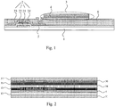
- Fig. 1 is a schematic diagram showing a display substrate according to an exemplary embodiment. As shown in Fig. 1 , the display substrate includes: a base 1, a thin film transistor 2, an organic light emitting layer 3 and a touch electrode layer 4.
- the material of the base may be glass.
- the material of the base may be flexible resin.
- the thin film transistor 2 is formed on a side of the base 1.
- the thin film transistor 2 may include structures such as a gate electrode 21, an active layer 22, a source electrode 23 and a drain electrode 24.
- a gate insulating layer 5 may also be provided between the gate electrode 21 and the active layer 22.
- the organic light emitting layer 3 is formed on a side of the thin film transistor 2 away from the base 1.
- the organic light emitting layer being formed on a side of the thin film transistor away from the base means that the organic light emitting layer is formed after the thin film transistor is formed.
- a passivation layer 6 may be provided between the organic light emitting layer 3 and the thin film transistor 2.
- the organic light emitting layer 3 is electrically connected to the thin film transistor through a via hole in the passivation layer 6.
- the thin film transistor may be formed by a patterning process, and the organic light emitting layer may be formed by a vapor deposition process.
- the relationship between sizes and positions of the organic light emitting layer and the thin film transistor is only an example, which may be adjusted as needed. For example, an area of the organic light emitting layer is increased, so that the organic light emitting layer also lies above the thin film transistor.
- a pixel defining layer may also be provided between the sub-pixels constituted by the organic light emitting layer, which will not be repeated in the present disclosure.
- the touch electrode layer 4 is formed in the organic light emitting layer 3.
- the organic light emitting layer may include a multi-layer structure, and the touching electrode layer may be formed between two adjacent layers among the multi-layer structure.
- the touch electrode layer may be formed by a patterning process, and a wiring electrically connected to the touch electrode layer may be formed in the display substrate, which will not be repeated herein.
- a touch electrode layer is formed in the organic light emitting layer, which may increase the integration level of the display substrate.
- an area of the organic light emitting layer may be set to be larger, or even the organic light emitting layer may be disposed directly over the thin film transistor and thus a touch electrode layer is formed in the organic light emitting layer, which facilitates setting a the touch electrode layer with a larger size, and further senses touch signals in a larger range.
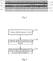
- Fig. 2 is a schematic diagram showing an organic light emitting layer according to an exemplary embodiment.
- the organic light emitting layer includes:
- the touch electrode layer is formed between the hole injection layer and the hole transport layer, or between the hole transport layer and the organic material layer, or between the organic material layer and the electron transport layer, or between the electron transport layer and the electron injection layer.
- the touch electrode layer 4 may be disposed between the hole injection layer 32 and the hole transport layer 33.
- a positive voltage may be applied to the anode layer
- a negative voltage may be applied to the cathode layer, thus forming a current flowing from the anode layer to the cathode layer. Electrons from the cathode layer sequentially pass through the electron injection layer, the electron transport layer, the organic material layer, the hole transport layer, the hole injection layer, reach the anode layer, and excite the organic material in the organic material layer to emit light when electrons pass through the organic material layer.
- the organic material layers in all of the sub-pixels emit white light when being excited.
- a color filter such as a red filter, a green filter and a blue filter, is required to be provided in a substrate arranged corresponding to the display substrate, so that the lights emitted from the sub-pixels corresponding to the filters with different colors are different in color, and thus the light emission color of the corresponding pixel may be changed by adjusting the light emission intensity of the sub-pixel.
- the organic material layers in different sub-pixels emit lights with different colors when being excited, for example, they may emit red light, green light and blue light respectively, so that the lights emitted from different sub-pixels are different in color, and thus the light emission color of the corresponding pixel may be changed by adjusting the light emission intensity of the sub-pixel.
- an anode may be formed by transparent conductive material and a cathode may be formed by conductive material with a high reflectivity, so that the light may be emitted from the bottom.
- a cathode may be formed by transparent conductive material and an anode may be formed by conductive material with a high reflectivity, so that the light may be emitted from the top.
- the transparent conductive material may be ITO (indium tin oxide), and the conductive material with a higher reflectivity may be a metal, such as aluminum or silver.
- Fig. 3 is a schematic diagram showing an organic light emitting layer according to another exemplary embodiment.
- An insulating layer 7 is disposed between the touch electrode layer 4 and a layer structure adjacent to the touch electrode layer 4.
- an insulating layer may be provided between the touch electrode layer 4 and the hole injection layer 32, and between the touch electrode layer 4 and the hole transport layer 33. Since there are electrons flowing from the cathode layer to the anode layer in respective layer structures in the organic light emitting layer, and electrons may stay in the layer structure adjacent to the touch electrode layer, thereby touch signals generated by the touch electrode layer may be affected.
- An insulating layer is provided between the touch electrode layer and a layer structure adjacent thereto, so that the touch electrode layer may be less influenced by other layer structures, thereby the accuracy of sensing touch operation of the touch electrode may be improved.
- the touch electrode layer is a self-induction capacitor.
- the cathode layer when a user touches the display device where the above display substrate is applied in, the cathode layer will be located between a finger and the touch electrode layer, thereby generating a shielding effect on the touch signal generated by sensing of the touch electrode layer.
- the intensity of touch signals generated by the self-induction capacitor sensing the touch operation is large, which is more conducive to obtain accurate touch results.
- the present disclosure further provides embodiments of a method for manufacturing a display substrate.
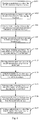
- Fig. 4 is a flow chart showing a method for manufacturing a display substrate according to an exemplary embodiment. As shown in Fig. 4 , the method includes following steps.
- a thin film transistor is formed on a base.
- an organic light emitting layer is formed on a side of the thin film transistor away from the base.
- a touch electrode layer is formed in the organic light emitting layer.
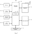
- Fig. 5 is a flow chart showing a method for manufacturing a display substrate according to another exemplary embodiment.
- the forming an organic light emitting layer on a side of the thin film transistor away from the base includes following steps.
- an anode layer is formed on a side of the thin film transistor away from the base.
- a hole injection layer is formed on a side of the anode layer away from the thin film transistor.
- a hole transport layer is formed on a side of the hole injection layer away from the anode layer.
- an organic material layer is formed on a side of the hole transport layer away from the hole injection layer.
- an electron transport layer is formed on a side of the organic material layer away from the hole transport layer.
- an electron injection layer is formed on a side of the electron transport layer away from the organic material layer.
- a cathode layer is formed on a side of the electron injection layer away from the electron transport layer.
- Forming the touch electrode layer in the organic light emitting layer includes:
- Fig. 6 is a flow chart showing a method for manufacturing a display substrate according to yet another exemplary embodiment.
- the above manufacturing method further includes: at step S44, forming an insulating layer between the touch electrode layer and a layer structure adjacent to the touch electrode layer.
- step S43 may be performed between step S422 and step S423
- step S44 may be performed between step S422 and step S44, and step S423 and step S44.
- the touch electrode layer is a self-induction capacitor.
- Fig. 7 is a schematic diagram showing a display device 700 according to an exemplary embodiment.
- the device 700 may be a mobile phone, a computer, a digital broadcast terminal, a messaging device, a gaming console, a tablet, a medical device, exercise equipment, a personal digital assistant, and the like.
- the device 700 may include one or more of the following components: a processing component 702, a memory 704, a power component 706, a multimedia component 708, an audio component 710, an input/output (I/O) interface 712, a sensor component 714, and a communication component 716.
- a processing component 702 a memory 704
- a power component 706 a multimedia component 708, an audio component 710, an input/output (I/O) interface 712, a sensor component 714, and a communication component 716.
- I/O input/output
- the processing component 702 typically controls overall operations of the device 700, such as the operations associated with display, telephone calls, data communications, camera operations, and recording operations.
- the processing component 702 may include one or more processors 720 to execute instructions.
- the processing component 702 may include one or more modules which facilitate the interaction between the processing component 702 and other components.
- the processing component 702 may include a multimedia module to facilitate the interaction between the multimedia component 708 and the processing component 702.
- the memory 704 is configured to store various types of data to support the operation of the device 700. Examples of such data include instructions for any applications or methods operated on the device 700, contact data, phonebook data, messages, pictures, video, etc.
- the memory 704 may be implemented using any type of volatile or non-volatile memory devices, or a combination thereof, such as a static random access memory (SRAM), an electrically erasable programmable read-only memory (EEPROM), an erasable programmable read-only memory (EPROM), a programmable read-only memory (PROM), a read-only memory (ROM), a magnetic memory, a flash memory, a magnetic or optical disk.
- SRAM static random access memory
- EEPROM electrically erasable programmable read-only memory
- EPROM erasable programmable read-only memory
- PROM programmable read-only memory
- ROM read-only memory
- magnetic memory a magnetic memory
- flash memory a flash memory
- magnetic or optical disk a magnetic or optical
- the power component 706 provides power to various components of the device 700.
- the power component 706 may include a power management system, one or more power sources, and any other components associated with the generation, management, and distribution of power in the device 700.
- the multimedia component 708 includes a screen providing an output interface between the device 700 and the user.
- the screen may include a liquid crystal display (LCD) and a touch panel (TP). If the screen includes the touch panel, the screen may be implemented as a touch screen to receive input signals from the user.
- the touch panel includes one or more touch sensors to sense touches, swipes, and gestures on the touch panel. The touch sensors may not only sense a boundary of a touch or swipe action, but also sense a period of time and a pressure associated with the touch or swipe action.
- the multimedia component 708 includes a front camera and/or a rear camera.
- the front camera and/or the rear camera may receive an external multimedia datum while the device 700 is in an operation mode, such as a photographing mode or a video mode.
- an operation mode such as a photographing mode or a video mode.
- Each of the front camera and the rear camera may be a fixed optical lens system or have focus and optical zoom capability.
- the audio component 710 is configured to output and/or input audio signals.
- the audio component 710 includes a microphone ("MIC") configured to receive an external audio signal when the device 700 is in an operation mode, such as a call mode, a recording mode, and a voice recognition mode.
- the received audio signal may be further stored in the memory 704 or transmitted via the communication component 716.
- the audio component 710 further includes a speaker to output audio signals.
- the I/O interface 712 provides an interface between the processing component 702 and peripheral interface modules, such as a keyboard, a click wheel, buttons, and the like.
- the buttons may include, but are not limited to, a home button, a volume button, a starting button, and a locking button.
- the sensor component 714 includes one or more sensors to provide status assessments of various aspects of the device 700. For instance, the sensor component 714 may detect an open/closed status of the device 700, relative positioning of components, e.g., the display and the keypad, of the device 700, a change in position of the device 700 or a component of the device 700, a presence or absence of user contact with the device 700, an orientation or an acceleration/deceleration of the device 700, and a change in temperature of the device 700.
- the sensor component 714 may include a proximity sensor configured to detect the presence of nearby objects without any physical contact.
- the sensor component 714 may further include a light sensor, such as a CMOS or CCD image sensor, for use in imaging applications.
- the sensor component 714 may further include an accelerometer sensor, a gyroscope sensor, a magnetic sensor, a pressure sensor or a temperature sensor.
- the communication component 716 is configured to facilitate communication, wired or wirelessly, between the device 700 and other devices.
- the device 700 may access a wireless network based on a communication standard, such as WiFi, 2G, or 3G, or a combination thereof.
- the communication component 716 receives a broadcast signal or broadcast associated information from an external broadcast management system via a broadcast channel.
- the communication component 716 further includes a near field communication (NFC) module to facilitate short-range communications.
- the NFC module may be implemented based on a radio frequency identification (RFID) technology, an infrared data association (IrDA) technology, an ultra-wideband (UWB) technology, a Bluetooth (BT) technology, and other technologies.
- RFID radio frequency identification
- IrDA infrared data association
- UWB ultra-wideband
- BT Bluetooth
- the device 700 may be implemented with one or more application specific integrated circuits (ASICs), digital signal processors (DSPs), digital signal processing devices (DSPDs), programmable logic devices (PLDs), field programmable gate arrays (FPGAs), controllers, micro-controllers, microprocessors, or other electronic components.
- ASICs application specific integrated circuits
- DSPs digital signal processors
- DSPDs digital signal processing devices
- PLDs programmable logic devices
- FPGAs field programmable gate arrays
- controllers micro-controllers, microprocessors, or other electronic components.
- non-transitory computer-readable storage medium including instructions, such as included in the memory 704, executable by the processor 720 in the device 700.
- the non-transitory computer-readable storage medium may be a ROM, a RAM, a CD-ROM, a magnetic tape, a floppy disc, an optical data storage device, and the like.
Landscapes
- Engineering & Computer Science (AREA)
- Physics & Mathematics (AREA)
- General Engineering & Computer Science (AREA)
- Theoretical Computer Science (AREA)
- Optics & Photonics (AREA)
- Human Computer Interaction (AREA)
- General Physics & Mathematics (AREA)
- Manufacturing & Machinery (AREA)
- Devices For Indicating Variable Information By Combining Individual Elements (AREA)
- Microelectronics & Electronic Packaging (AREA)
- Electroluminescent Light Sources (AREA)
Applications Claiming Priority (1)
| Application Number | Priority Date | Filing Date | Title |
|---|---|---|---|
| CN201610957966.3A CN106356394B (zh) | 2016-10-27 | 2016-10-27 | 显示基板及其制作方法和电子设备 |
Publications (2)
| Publication Number | Publication Date |
|---|---|
| EP3316331A1 EP3316331A1 (en) | 2018-05-02 |
| EP3316331B1 true EP3316331B1 (en) | 2020-12-02 |
Family
ID=57865150
Family Applications (1)
| Application Number | Title | Priority Date | Filing Date |
|---|---|---|---|
| EP17198792.8A Active EP3316331B1 (en) | 2016-10-27 | 2017-10-27 | Display substrate, method for manufacturing the same and electronic apparatus |
Country Status (7)
| Country | Link |
|---|---|
| US (2) | US10516005B2 (enExample) |
| EP (1) | EP3316331B1 (enExample) |
| JP (1) | JP6976845B2 (enExample) |
| KR (1) | KR102118467B1 (enExample) |
| CN (1) | CN106356394B (enExample) |
| RU (1) | RU2665816C1 (enExample) |
| WO (1) | WO2018076505A1 (enExample) |
Families Citing this family (8)
| Publication number | Priority date | Publication date | Assignee | Title |
|---|---|---|---|---|
| CN106876604A (zh) | 2017-02-14 | 2017-06-20 | 鄂尔多斯市源盛光电有限责任公司 | 有机发光二极管器件及其制造方法 |
| CN106851942B (zh) * | 2017-03-02 | 2019-08-23 | 武汉金石微电子技术有限公司 | 一种自感应节能智能发光墙纸及其应用方法 |
| CN107561721A (zh) * | 2017-08-30 | 2018-01-09 | 京东方科技集团股份有限公司 | 透明真3d显示器 |
| CN108183121A (zh) * | 2017-12-15 | 2018-06-19 | 武汉华星光电半导体显示技术有限公司 | 柔性显示面板及其制作方法 |
| CN110518146B (zh) | 2019-08-30 | 2022-02-25 | 京东方科技集团股份有限公司 | 薄膜封装结构及显示面板 |
| CN112286398A (zh) * | 2020-11-18 | 2021-01-29 | 武汉华星光电半导体显示技术有限公司 | 触控面板及显示装置 |
| CN112785927B (zh) * | 2021-01-28 | 2024-01-19 | 维沃移动通信有限公司 | 电子设备及显示模组 |
| KR20250122246A (ko) * | 2024-02-06 | 2025-08-13 | 엘지디스플레이 주식회사 | 인셀 터치 표시 장치 |
Family Cites Families (32)
| Publication number | Priority date | Publication date | Assignee | Title |
|---|---|---|---|---|
| JP3284259B2 (ja) | 1996-03-14 | 2002-05-20 | 松下電工株式会社 | El照光式タッチスイッチ |
| KR100573154B1 (ko) * | 2004-06-26 | 2006-04-24 | 삼성에스디아이 주식회사 | 전계 발광 디스플레이 장치 및 이의 제조 방법 |
| CN100379056C (zh) | 2005-03-01 | 2008-04-02 | 友达光电股份有限公司 | 具有触控功能的平面显示器及其形成方法 |
| CN1652651A (zh) | 2005-03-23 | 2005-08-10 | 友达光电股份有限公司 | 触控式有机发光显示器 |
| FR2913146B1 (fr) * | 2007-02-23 | 2009-05-01 | Saint Gobain | Electrode discontinue, dispositif electroluminescent organique l'incorporant, et leurs fabrications |
| JP4464985B2 (ja) | 2007-04-27 | 2010-05-19 | ビステオン・ジャパン株式会社 | El発光式タッチスイッチ |
| KR101045264B1 (ko) | 2008-09-09 | 2011-06-29 | 네오뷰코오롱 주식회사 | 디스플레이 장치, 이를 구비하는 모바일 기기 및 디스플레이 제어 방법 |
| JP5157825B2 (ja) * | 2008-10-29 | 2013-03-06 | ソニー株式会社 | 有機elディスプレイの製造方法 |
| CN101894856B (zh) | 2009-05-22 | 2013-11-06 | 上海天马微电子有限公司 | 一种有机发光二极管显示屏和触控检测单元 |
| KR101633104B1 (ko) * | 2009-08-27 | 2016-06-24 | 엘지디스플레이 주식회사 | 유기전계발광표시장치 |
| KR101588450B1 (ko) * | 2009-10-23 | 2016-01-25 | 엘지디스플레이 주식회사 | 터치 센서 인셀 타입 유기전계 발광소자 |
| KR101696483B1 (ko) * | 2010-12-06 | 2017-01-13 | 엘지디스플레이 주식회사 | 유기 발광 다이오드 표시장치 |
| TWI534664B (zh) | 2011-07-28 | 2016-05-21 | 宸鴻光電科技股份有限公司 | 觸控顯示裝置 |
| JP5726804B2 (ja) * | 2012-04-19 | 2015-06-03 | 株式会社東芝 | 表示パネル及び表示装置 |
| KR101967290B1 (ko) * | 2012-11-14 | 2019-04-09 | 엘지디스플레이 주식회사 | 인셀-터치 타입 유기발광다이오드 표시장치 |
| CN103050506A (zh) | 2012-12-28 | 2013-04-17 | 南京中电熊猫液晶显示科技有限公司 | 一种oled显示器 |
| KR102096622B1 (ko) * | 2013-08-19 | 2020-04-03 | 삼성디스플레이 주식회사 | 유기발광 표시장치 |
| KR102124906B1 (ko) * | 2013-12-26 | 2020-07-07 | 엘지디스플레이 주식회사 | 터치스크린을 구비한 유기전계 발광소자 및 이의 제조 방법 |
| CN104752466B (zh) | 2013-12-30 | 2019-06-04 | 昆山国显光电有限公司 | 一种整合触屏功能的有机发光显示装置及其制造方法 |
| CN105446554A (zh) * | 2014-05-27 | 2016-03-30 | 上海和辉光电有限公司 | 有机电激发光装置 |
| CN105493626B (zh) | 2014-06-06 | 2017-05-03 | 柯尼卡美能达株式会社 | 有机电致发光模块、智能设备及照明装置 |
| CN104409467B (zh) * | 2014-10-13 | 2018-04-24 | 上海天马有机发光显示技术有限公司 | 一种触控面板及其制作方法和显示装置 |
| CN105590951B (zh) * | 2014-11-10 | 2019-04-09 | 乐金显示有限公司 | 具有多模腔结构的有机发光二极管显示器 |
| KR102269919B1 (ko) * | 2014-12-12 | 2021-06-28 | 삼성디스플레이 주식회사 | 터치 센서를 포함하는 표시 장치 |
| CN106033765B (zh) * | 2015-03-17 | 2019-06-11 | 上海和辉光电有限公司 | 有机发光二极管触控显示面板 |
| CN104795425A (zh) | 2015-03-30 | 2015-07-22 | 京东方科技集团股份有限公司 | 有机发光二极管触控显示屏及其制作方法 |
| KR102341352B1 (ko) * | 2015-04-08 | 2021-12-20 | 삼성디스플레이 주식회사 | 터치 센서를 포함하는 표시 장치 |
| CN104850268B (zh) | 2015-06-10 | 2018-02-06 | 京东方科技集团股份有限公司 | 一种触控显示面板、触控显示装置及制作方法 |
| CN104881179B (zh) | 2015-06-23 | 2017-07-28 | 京东方科技集团股份有限公司 | 一种内嵌式触摸显示屏、其驱动方法及显示装置 |
| CN104898887B (zh) * | 2015-06-23 | 2017-10-17 | 京东方科技集团股份有限公司 | 一种内嵌式触摸显示屏、其驱动方法及显示装置 |
| EP3350837B1 (en) * | 2015-09-15 | 2022-04-06 | BOE Technology Group Co., Ltd. | Array substrate, related display panels, and related display apparatus |
| CN105243993B (zh) | 2015-09-22 | 2018-01-26 | 京东方科技集团股份有限公司 | Oled显示基板及其驱动方法和oled显示装置 |
-
2016
- 2016-10-27 CN CN201610957966.3A patent/CN106356394B/zh active Active
- 2016-12-20 JP JP2017510653A patent/JP6976845B2/ja active Active
- 2016-12-20 KR KR1020187032410A patent/KR102118467B1/ko active Active
- 2016-12-20 WO PCT/CN2016/110999 patent/WO2018076505A1/zh not_active Ceased
- 2016-12-20 RU RU2017134748A patent/RU2665816C1/ru active
-
2017
- 2017-10-25 US US15/792,926 patent/US10516005B2/en active Active
- 2017-10-27 EP EP17198792.8A patent/EP3316331B1/en active Active
-
2019
- 2019-10-15 US US16/653,074 patent/US10818736B2/en active Active
Non-Patent Citations (1)
| Title |
|---|
| None * |
Also Published As
| Publication number | Publication date |
|---|---|
| JP2018538553A (ja) | 2018-12-27 |
| US10818736B2 (en) | 2020-10-27 |
| EP3316331A1 (en) | 2018-05-02 |
| CN106356394B (zh) | 2018-09-04 |
| KR20180135919A (ko) | 2018-12-21 |
| KR102118467B1 (ko) | 2020-06-10 |
| CN106356394A (zh) | 2017-01-25 |
| RU2665816C1 (ru) | 2018-09-04 |
| US10516005B2 (en) | 2019-12-24 |
| US20200043985A1 (en) | 2020-02-06 |
| WO2018076505A1 (zh) | 2018-05-03 |
| US20180122865A1 (en) | 2018-05-03 |
| JP6976845B2 (ja) | 2021-12-08 |
Similar Documents
| Publication | Publication Date | Title |
|---|---|---|
| EP3316331B1 (en) | Display substrate, method for manufacturing the same and electronic apparatus | |
| CN106372625B (zh) | 显示基板及其制作方法和电子设备 | |
| US11538872B2 (en) | Display structure, display panel using the same and display device using the same | |
| US11417270B2 (en) | Organic light-emitting diode display, display control method and electronic device | |
| CN106970495A (zh) | 阵列基板及其制作方法、显示面板、显示装置和电子设备 | |
| CN110944069B (zh) | 终端屏幕及其控制方法、装置和终端 | |
| CN107886038A (zh) | 显示装置和电子设备 | |
| US20200105187A1 (en) | Display structure, display panel and display device | |
| EP3477704B1 (en) | Camera photosensitive component, camera, and camera shooting terminal | |
| CN107885002A (zh) | 显示面板、显示装置、阵列基板的制作方法和电子设备 | |
| CN107884968A (zh) | 阵列基板及其制作方法、显示面板、显示装置和电子设备 | |
| CN106919914B (zh) | 显示模组和电子设备 | |
| CN107886031A (zh) | 显示装置和电子设备 | |
| CN112185302A (zh) | 显示器和显示装置 | |
| CN108847199A (zh) | 亮度确定方法及装置 | |
| CN111384092B (zh) | 终端和有机发光二极管显示面板的制作方法 | |
| CN111384095B (zh) | 一种终端 | |
| CN107153301A (zh) | 背光模组、显示模组和电子设备 | |
| CN106782119A (zh) | 显示模组和电子设备 | |
| CN219019447U (zh) | 显示屏和终端 | |
| CN111381795B (zh) | 显示控制方法、装置、电子设备和计算机可读存储介质 | |
| CN106597729A (zh) | 彩膜基板及其制作方法、显示面板和电子设备 | |
| CN111384089A (zh) | 显示面板和终端 | |
| CN111443758A (zh) | 显示控制方法、装置、电子设备和计算机可读存储介质 |
Legal Events
| Date | Code | Title | Description |
|---|---|---|---|
| PUAI | Public reference made under article 153(3) epc to a published international application that has entered the european phase |
Free format text: ORIGINAL CODE: 0009012 |
|
| STAA | Information on the status of an ep patent application or granted ep patent |
Free format text: STATUS: THE APPLICATION HAS BEEN PUBLISHED |
|
| AK | Designated contracting states |
Kind code of ref document: A1 Designated state(s): AL AT BE BG CH CY CZ DE DK EE ES FI FR GB GR HR HU IE IS IT LI LT LU LV MC MK MT NL NO PL PT RO RS SE SI SK SM TR |
|
| AX | Request for extension of the european patent |
Extension state: BA ME |
|
| STAA | Information on the status of an ep patent application or granted ep patent |
Free format text: STATUS: REQUEST FOR EXAMINATION WAS MADE |
|
| 17P | Request for examination filed |
Effective date: 20181030 |
|
| RBV | Designated contracting states (corrected) |
Designated state(s): AL AT BE BG CH CY CZ DE DK EE ES FI FR GB GR HR HU IE IS IT LI LT LU LV MC MK MT NL NO PL PT RO RS SE SI SK SM TR |
|
| GRAP | Despatch of communication of intention to grant a patent |
Free format text: ORIGINAL CODE: EPIDOSNIGR1 |
|
| STAA | Information on the status of an ep patent application or granted ep patent |
Free format text: STATUS: GRANT OF PATENT IS INTENDED |
|
| RIC1 | Information provided on ipc code assigned before grant |
Ipc: H01L 27/32 20060101ALI20200603BHEP Ipc: H01L 51/52 20060101AFI20200603BHEP |
|
| INTG | Intention to grant announced |
Effective date: 20200626 |
|
| GRAS | Grant fee paid |
Free format text: ORIGINAL CODE: EPIDOSNIGR3 |
|
| GRAA | (expected) grant |
Free format text: ORIGINAL CODE: 0009210 |
|
| STAA | Information on the status of an ep patent application or granted ep patent |
Free format text: STATUS: THE PATENT HAS BEEN GRANTED |
|
| AK | Designated contracting states |
Kind code of ref document: B1 Designated state(s): AL AT BE BG CH CY CZ DE DK EE ES FI FR GB GR HR HU IE IS IT LI LT LU LV MC MK MT NL NO PL PT RO RS SE SI SK SM TR |
|
| REG | Reference to a national code |
Ref country code: GB Ref legal event code: FG4D |
|
| REG | Reference to a national code |
Ref country code: AT Ref legal event code: REF Ref document number: 1341895 Country of ref document: AT Kind code of ref document: T Effective date: 20201215 Ref country code: CH Ref legal event code: EP |
|
| REG | Reference to a national code |
Ref country code: DE Ref legal event code: R096 Ref document number: 602017028692 Country of ref document: DE |
|
| REG | Reference to a national code |
Ref country code: IE Ref legal event code: FG4D |
|
| PG25 | Lapsed in a contracting state [announced via postgrant information from national office to epo] |
Ref country code: GR Free format text: LAPSE BECAUSE OF FAILURE TO SUBMIT A TRANSLATION OF THE DESCRIPTION OR TO PAY THE FEE WITHIN THE PRESCRIBED TIME-LIMIT Effective date: 20210303 Ref country code: FI Free format text: LAPSE BECAUSE OF FAILURE TO SUBMIT A TRANSLATION OF THE DESCRIPTION OR TO PAY THE FEE WITHIN THE PRESCRIBED TIME-LIMIT Effective date: 20201202 Ref country code: NO Free format text: LAPSE BECAUSE OF FAILURE TO SUBMIT A TRANSLATION OF THE DESCRIPTION OR TO PAY THE FEE WITHIN THE PRESCRIBED TIME-LIMIT Effective date: 20210302 Ref country code: RS Free format text: LAPSE BECAUSE OF FAILURE TO SUBMIT A TRANSLATION OF THE DESCRIPTION OR TO PAY THE FEE WITHIN THE PRESCRIBED TIME-LIMIT Effective date: 20201202 |
|
| REG | Reference to a national code |
Ref country code: NL Ref legal event code: MP Effective date: 20201202 |
|
| REG | Reference to a national code |
Ref country code: AT Ref legal event code: MK05 Ref document number: 1341895 Country of ref document: AT Kind code of ref document: T Effective date: 20201202 |
|
| PG25 | Lapsed in a contracting state [announced via postgrant information from national office to epo] |
Ref country code: SE Free format text: LAPSE BECAUSE OF FAILURE TO SUBMIT A TRANSLATION OF THE DESCRIPTION OR TO PAY THE FEE WITHIN THE PRESCRIBED TIME-LIMIT Effective date: 20201202 Ref country code: BG Free format text: LAPSE BECAUSE OF FAILURE TO SUBMIT A TRANSLATION OF THE DESCRIPTION OR TO PAY THE FEE WITHIN THE PRESCRIBED TIME-LIMIT Effective date: 20210302 Ref country code: LV Free format text: LAPSE BECAUSE OF FAILURE TO SUBMIT A TRANSLATION OF THE DESCRIPTION OR TO PAY THE FEE WITHIN THE PRESCRIBED TIME-LIMIT Effective date: 20201202 Ref country code: PL Free format text: LAPSE BECAUSE OF FAILURE TO SUBMIT A TRANSLATION OF THE DESCRIPTION OR TO PAY THE FEE WITHIN THE PRESCRIBED TIME-LIMIT Effective date: 20201202 |
|
| PG25 | Lapsed in a contracting state [announced via postgrant information from national office to epo] |
Ref country code: HR Free format text: LAPSE BECAUSE OF FAILURE TO SUBMIT A TRANSLATION OF THE DESCRIPTION OR TO PAY THE FEE WITHIN THE PRESCRIBED TIME-LIMIT Effective date: 20201202 Ref country code: NL Free format text: LAPSE BECAUSE OF FAILURE TO SUBMIT A TRANSLATION OF THE DESCRIPTION OR TO PAY THE FEE WITHIN THE PRESCRIBED TIME-LIMIT Effective date: 20201202 |
|
| REG | Reference to a national code |
Ref country code: LT Ref legal event code: MG9D |
|
| PG25 | Lapsed in a contracting state [announced via postgrant information from national office to epo] |
Ref country code: SM Free format text: LAPSE BECAUSE OF FAILURE TO SUBMIT A TRANSLATION OF THE DESCRIPTION OR TO PAY THE FEE WITHIN THE PRESCRIBED TIME-LIMIT Effective date: 20201202 Ref country code: LT Free format text: LAPSE BECAUSE OF FAILURE TO SUBMIT A TRANSLATION OF THE DESCRIPTION OR TO PAY THE FEE WITHIN THE PRESCRIBED TIME-LIMIT Effective date: 20201202 Ref country code: CZ Free format text: LAPSE BECAUSE OF FAILURE TO SUBMIT A TRANSLATION OF THE DESCRIPTION OR TO PAY THE FEE WITHIN THE PRESCRIBED TIME-LIMIT Effective date: 20201202 Ref country code: EE Free format text: LAPSE BECAUSE OF FAILURE TO SUBMIT A TRANSLATION OF THE DESCRIPTION OR TO PAY THE FEE WITHIN THE PRESCRIBED TIME-LIMIT Effective date: 20201202 Ref country code: RO Free format text: LAPSE BECAUSE OF FAILURE TO SUBMIT A TRANSLATION OF THE DESCRIPTION OR TO PAY THE FEE WITHIN THE PRESCRIBED TIME-LIMIT Effective date: 20201202 Ref country code: PT Free format text: LAPSE BECAUSE OF FAILURE TO SUBMIT A TRANSLATION OF THE DESCRIPTION OR TO PAY THE FEE WITHIN THE PRESCRIBED TIME-LIMIT Effective date: 20210405 Ref country code: SK Free format text: LAPSE BECAUSE OF FAILURE TO SUBMIT A TRANSLATION OF THE DESCRIPTION OR TO PAY THE FEE WITHIN THE PRESCRIBED TIME-LIMIT Effective date: 20201202 |
|
| PG25 | Lapsed in a contracting state [announced via postgrant information from national office to epo] |
Ref country code: AT Free format text: LAPSE BECAUSE OF FAILURE TO SUBMIT A TRANSLATION OF THE DESCRIPTION OR TO PAY THE FEE WITHIN THE PRESCRIBED TIME-LIMIT Effective date: 20201202 |
|
| REG | Reference to a national code |
Ref country code: DE Ref legal event code: R097 Ref document number: 602017028692 Country of ref document: DE |
|
| PG25 | Lapsed in a contracting state [announced via postgrant information from national office to epo] |
Ref country code: IS Free format text: LAPSE BECAUSE OF FAILURE TO SUBMIT A TRANSLATION OF THE DESCRIPTION OR TO PAY THE FEE WITHIN THE PRESCRIBED TIME-LIMIT Effective date: 20210402 |
|
| PLBE | No opposition filed within time limit |
Free format text: ORIGINAL CODE: 0009261 |
|
| STAA | Information on the status of an ep patent application or granted ep patent |
Free format text: STATUS: NO OPPOSITION FILED WITHIN TIME LIMIT |
|
| PG25 | Lapsed in a contracting state [announced via postgrant information from national office to epo] |
Ref country code: IT Free format text: LAPSE BECAUSE OF FAILURE TO SUBMIT A TRANSLATION OF THE DESCRIPTION OR TO PAY THE FEE WITHIN THE PRESCRIBED TIME-LIMIT Effective date: 20201202 Ref country code: AL Free format text: LAPSE BECAUSE OF FAILURE TO SUBMIT A TRANSLATION OF THE DESCRIPTION OR TO PAY THE FEE WITHIN THE PRESCRIBED TIME-LIMIT Effective date: 20201202 |
|
| 26N | No opposition filed |
Effective date: 20210903 |
|
| PG25 | Lapsed in a contracting state [announced via postgrant information from national office to epo] |
Ref country code: DK Free format text: LAPSE BECAUSE OF FAILURE TO SUBMIT A TRANSLATION OF THE DESCRIPTION OR TO PAY THE FEE WITHIN THE PRESCRIBED TIME-LIMIT Effective date: 20201202 Ref country code: SI Free format text: LAPSE BECAUSE OF FAILURE TO SUBMIT A TRANSLATION OF THE DESCRIPTION OR TO PAY THE FEE WITHIN THE PRESCRIBED TIME-LIMIT Effective date: 20201202 |
|
| PG25 | Lapsed in a contracting state [announced via postgrant information from national office to epo] |
Ref country code: ES Free format text: LAPSE BECAUSE OF FAILURE TO SUBMIT A TRANSLATION OF THE DESCRIPTION OR TO PAY THE FEE WITHIN THE PRESCRIBED TIME-LIMIT Effective date: 20201202 |
|
| REG | Reference to a national code |
Ref country code: CH Ref legal event code: PL |
|
| PG25 | Lapsed in a contracting state [announced via postgrant information from national office to epo] |
Ref country code: IS Free format text: LAPSE BECAUSE OF FAILURE TO SUBMIT A TRANSLATION OF THE DESCRIPTION OR TO PAY THE FEE WITHIN THE PRESCRIBED TIME-LIMIT Effective date: 20210402 |
|
| REG | Reference to a national code |
Ref country code: BE Ref legal event code: MM Effective date: 20211031 |
|
| PG25 | Lapsed in a contracting state [announced via postgrant information from national office to epo] |
Ref country code: MC Free format text: LAPSE BECAUSE OF FAILURE TO SUBMIT A TRANSLATION OF THE DESCRIPTION OR TO PAY THE FEE WITHIN THE PRESCRIBED TIME-LIMIT Effective date: 20201202 |
|
| PG25 | Lapsed in a contracting state [announced via postgrant information from national office to epo] |
Ref country code: LU Free format text: LAPSE BECAUSE OF NON-PAYMENT OF DUE FEES Effective date: 20211027 Ref country code: BE Free format text: LAPSE BECAUSE OF NON-PAYMENT OF DUE FEES Effective date: 20211031 |
|
| PG25 | Lapsed in a contracting state [announced via postgrant information from national office to epo] |
Ref country code: LI Free format text: LAPSE BECAUSE OF NON-PAYMENT OF DUE FEES Effective date: 20211031 Ref country code: CH Free format text: LAPSE BECAUSE OF NON-PAYMENT OF DUE FEES Effective date: 20211031 |
|
| PG25 | Lapsed in a contracting state [announced via postgrant information from national office to epo] |
Ref country code: IE Free format text: LAPSE BECAUSE OF NON-PAYMENT OF DUE FEES Effective date: 20211027 |
|
| REG | Reference to a national code |
Ref country code: DE Ref legal event code: R079 Ref document number: 602017028692 Country of ref document: DE Free format text: PREVIOUS MAIN CLASS: H01L0051520000 Ipc: H10K0050800000 |
|
| PG25 | Lapsed in a contracting state [announced via postgrant information from national office to epo] |
Ref country code: HU Free format text: LAPSE BECAUSE OF FAILURE TO SUBMIT A TRANSLATION OF THE DESCRIPTION OR TO PAY THE FEE WITHIN THE PRESCRIBED TIME-LIMIT; INVALID AB INITIO Effective date: 20171027 |
|
| P01 | Opt-out of the competence of the unified patent court (upc) registered |
Effective date: 20230523 |
|
| PG25 | Lapsed in a contracting state [announced via postgrant information from national office to epo] |
Ref country code: CY Free format text: LAPSE BECAUSE OF FAILURE TO SUBMIT A TRANSLATION OF THE DESCRIPTION OR TO PAY THE FEE WITHIN THE PRESCRIBED TIME-LIMIT Effective date: 20201202 |
|
| PG25 | Lapsed in a contracting state [announced via postgrant information from national office to epo] |
Ref country code: MK Free format text: LAPSE BECAUSE OF FAILURE TO SUBMIT A TRANSLATION OF THE DESCRIPTION OR TO PAY THE FEE WITHIN THE PRESCRIBED TIME-LIMIT Effective date: 20201202 |
|
| PG25 | Lapsed in a contracting state [announced via postgrant information from national office to epo] |
Ref country code: TR Free format text: LAPSE BECAUSE OF FAILURE TO SUBMIT A TRANSLATION OF THE DESCRIPTION OR TO PAY THE FEE WITHIN THE PRESCRIBED TIME-LIMIT Effective date: 20201202 |
|
| PG25 | Lapsed in a contracting state [announced via postgrant information from national office to epo] |
Ref country code: MT Free format text: LAPSE BECAUSE OF FAILURE TO SUBMIT A TRANSLATION OF THE DESCRIPTION OR TO PAY THE FEE WITHIN THE PRESCRIBED TIME-LIMIT Effective date: 20201202 |
|
| PGFP | Annual fee paid to national office [announced via postgrant information from national office to epo] |
Ref country code: DE Payment date: 20241021 Year of fee payment: 8 |
|
| PGFP | Annual fee paid to national office [announced via postgrant information from national office to epo] |
Ref country code: GB Payment date: 20241025 Year of fee payment: 8 |
|
| PGFP | Annual fee paid to national office [announced via postgrant information from national office to epo] |
Ref country code: FR Payment date: 20241030 Year of fee payment: 8 |