EP3309928B1 - Système de transmission d'énergie à couplage inductif par résonance avec une réactance ajustable - Google Patents
Système de transmission d'énergie à couplage inductif par résonance avec une réactance ajustable Download PDFInfo
- Publication number
- EP3309928B1 EP3309928B1 EP17204148.5A EP17204148A EP3309928B1 EP 3309928 B1 EP3309928 B1 EP 3309928B1 EP 17204148 A EP17204148 A EP 17204148A EP 3309928 B1 EP3309928 B1 EP 3309928B1
- Authority
- EP
- European Patent Office
- Prior art keywords
- voltage waveform
- amplitude
- square wave
- power
- reactance
- Prior art date
- Legal status (The legal status is an assumption and is not a legal conclusion. Google has not performed a legal analysis and makes no representation as to the accuracy of the status listed.)
- Active
Links
- 230000001939 inductive effect Effects 0.000 title claims description 24
- 230000005540 biological transmission Effects 0.000 title description 10
- 238000012546 transfer Methods 0.000 claims description 29
- 238000000034 method Methods 0.000 claims description 12
- 238000006243 chemical reaction Methods 0.000 claims description 9
- 230000000694 effects Effects 0.000 claims description 8
- 239000003990 capacitor Substances 0.000 description 12
- 230000033001 locomotion Effects 0.000 description 12
- 238000004804 winding Methods 0.000 description 12
- 238000013461 design Methods 0.000 description 7
- 238000006073 displacement reaction Methods 0.000 description 6
- 230000005291 magnetic effect Effects 0.000 description 6
- 238000004519 manufacturing process Methods 0.000 description 6
- 239000002131 composite material Substances 0.000 description 5
- 238000005516 engineering process Methods 0.000 description 5
- 238000013459 approach Methods 0.000 description 3
- 239000011162 core material Substances 0.000 description 3
- 238000001514 detection method Methods 0.000 description 3
- 239000004065 semiconductor Substances 0.000 description 3
- 238000000926 separation method Methods 0.000 description 3
- 239000000725 suspension Substances 0.000 description 3
- 230000000903 blocking effect Effects 0.000 description 2
- 230000008859 change Effects 0.000 description 2
- 238000012937 correction Methods 0.000 description 2
- 230000002349 favourable effect Effects 0.000 description 2
- 230000005669 field effect Effects 0.000 description 2
- 230000004907 flux Effects 0.000 description 2
- 230000006698 induction Effects 0.000 description 2
- 238000012423 maintenance Methods 0.000 description 2
- 238000005070 sampling Methods 0.000 description 2
- 230000035945 sensitivity Effects 0.000 description 2
- 230000009471 action Effects 0.000 description 1
- 230000004075 alteration Effects 0.000 description 1
- 230000003321 amplification Effects 0.000 description 1
- 230000002567 autonomic effect Effects 0.000 description 1
- 230000002457 bidirectional effect Effects 0.000 description 1
- 230000015572 biosynthetic process Effects 0.000 description 1
- 230000015556 catabolic process Effects 0.000 description 1
- 238000004891 communication Methods 0.000 description 1
- 238000013329 compounding Methods 0.000 description 1
- 238000012790 confirmation Methods 0.000 description 1
- 230000008602 contraction Effects 0.000 description 1
- 230000008878 coupling Effects 0.000 description 1
- 238000010168 coupling process Methods 0.000 description 1
- 238000005859 coupling reaction Methods 0.000 description 1
- 238000006731 degradation reaction Methods 0.000 description 1
- 230000002939 deleterious effect Effects 0.000 description 1
- 238000011161 development Methods 0.000 description 1
- 238000010586 diagram Methods 0.000 description 1
- 238000009826 distribution Methods 0.000 description 1
- 238000004146 energy storage Methods 0.000 description 1
- 230000005284 excitation Effects 0.000 description 1
- 230000006355 external stress Effects 0.000 description 1
- 230000005294 ferromagnetic effect Effects 0.000 description 1
- 238000001914 filtration Methods 0.000 description 1
- 230000007274 generation of a signal involved in cell-cell signaling Effects 0.000 description 1
- 238000010438 heat treatment Methods 0.000 description 1
- 230000007257 malfunction Effects 0.000 description 1
- 238000007726 management method Methods 0.000 description 1
- 239000000463 material Substances 0.000 description 1
- 238000012544 monitoring process Methods 0.000 description 1
- 238000003199 nucleic acid amplification method Methods 0.000 description 1
- 230000003534 oscillatory effect Effects 0.000 description 1
- 230000035699 permeability Effects 0.000 description 1
- 230000010363 phase shift Effects 0.000 description 1
- 230000008439 repair process Effects 0.000 description 1
- 230000000717 retained effect Effects 0.000 description 1
- 230000009291 secondary effect Effects 0.000 description 1
- 230000035939 shock Effects 0.000 description 1
- 238000012358 sourcing Methods 0.000 description 1
- 239000013589 supplement Substances 0.000 description 1
- 238000003786 synthesis reaction Methods 0.000 description 1
- 238000013519 translation Methods 0.000 description 1
- 229910000859 α-Fe Inorganic materials 0.000 description 1
Images

Classifications
-
- H02J5/005—
-
- H—ELECTRICITY
- H02—GENERATION; CONVERSION OR DISTRIBUTION OF ELECTRIC POWER
- H02J—CIRCUIT ARRANGEMENTS OR SYSTEMS FOR SUPPLYING OR DISTRIBUTING ELECTRIC POWER; SYSTEMS FOR STORING ELECTRIC ENERGY
- H02J50/00—Circuit arrangements or systems for wireless supply or distribution of electric power
- H02J50/10—Circuit arrangements or systems for wireless supply or distribution of electric power using inductive coupling
- H02J50/12—Circuit arrangements or systems for wireless supply or distribution of electric power using inductive coupling of the resonant type
-
- H—ELECTRICITY
- H01—ELECTRIC ELEMENTS
- H01F—MAGNETS; INDUCTANCES; TRANSFORMERS; SELECTION OF MATERIALS FOR THEIR MAGNETIC PROPERTIES
- H01F38/00—Adaptations of transformers or inductances for specific applications or functions
- H01F38/14—Inductive couplings
-
- H—ELECTRICITY
- H02—GENERATION; CONVERSION OR DISTRIBUTION OF ELECTRIC POWER
- H02J—CIRCUIT ARRANGEMENTS OR SYSTEMS FOR SUPPLYING OR DISTRIBUTING ELECTRIC POWER; SYSTEMS FOR STORING ELECTRIC ENERGY
- H02J50/00—Circuit arrangements or systems for wireless supply or distribution of electric power
- H02J50/10—Circuit arrangements or systems for wireless supply or distribution of electric power using inductive coupling
-
- Y—GENERAL TAGGING OF NEW TECHNOLOGICAL DEVELOPMENTS; GENERAL TAGGING OF CROSS-SECTIONAL TECHNOLOGIES SPANNING OVER SEVERAL SECTIONS OF THE IPC; TECHNICAL SUBJECTS COVERED BY FORMER USPC CROSS-REFERENCE ART COLLECTIONS [XRACs] AND DIGESTS
- Y02—TECHNOLOGIES OR APPLICATIONS FOR MITIGATION OR ADAPTATION AGAINST CLIMATE CHANGE
- Y02B—CLIMATE CHANGE MITIGATION TECHNOLOGIES RELATED TO BUILDINGS, e.g. HOUSING, HOUSE APPLIANCES OR RELATED END-USER APPLICATIONS
- Y02B70/00—Technologies for an efficient end-user side electric power management and consumption
- Y02B70/10—Technologies improving the efficiency by using switched-mode power supplies [SMPS], i.e. efficient power electronics conversion e.g. power factor correction or reduction of losses in power supplies or efficient standby modes
-
- Y—GENERAL TAGGING OF NEW TECHNOLOGICAL DEVELOPMENTS; GENERAL TAGGING OF CROSS-SECTIONAL TECHNOLOGIES SPANNING OVER SEVERAL SECTIONS OF THE IPC; TECHNICAL SUBJECTS COVERED BY FORMER USPC CROSS-REFERENCE ART COLLECTIONS [XRACs] AND DIGESTS
- Y02—TECHNOLOGIES OR APPLICATIONS FOR MITIGATION OR ADAPTATION AGAINST CLIMATE CHANGE
- Y02T—CLIMATE CHANGE MITIGATION TECHNOLOGIES RELATED TO TRANSPORTATION
- Y02T10/00—Road transport of goods or passengers
- Y02T10/60—Other road transportation technologies with climate change mitigation effect
- Y02T10/70—Energy storage systems for electromobility, e.g. batteries
-
- Y—GENERAL TAGGING OF NEW TECHNOLOGICAL DEVELOPMENTS; GENERAL TAGGING OF CROSS-SECTIONAL TECHNOLOGIES SPANNING OVER SEVERAL SECTIONS OF THE IPC; TECHNICAL SUBJECTS COVERED BY FORMER USPC CROSS-REFERENCE ART COLLECTIONS [XRACs] AND DIGESTS
- Y02—TECHNOLOGIES OR APPLICATIONS FOR MITIGATION OR ADAPTATION AGAINST CLIMATE CHANGE
- Y02T—CLIMATE CHANGE MITIGATION TECHNOLOGIES RELATED TO TRANSPORTATION
- Y02T10/00—Road transport of goods or passengers
- Y02T10/60—Other road transportation technologies with climate change mitigation effect
- Y02T10/7072—Electromobility specific charging systems or methods for batteries, ultracapacitors, supercapacitors or double-layer capacitors
-
- Y—GENERAL TAGGING OF NEW TECHNOLOGICAL DEVELOPMENTS; GENERAL TAGGING OF CROSS-SECTIONAL TECHNOLOGIES SPANNING OVER SEVERAL SECTIONS OF THE IPC; TECHNICAL SUBJECTS COVERED BY FORMER USPC CROSS-REFERENCE ART COLLECTIONS [XRACs] AND DIGESTS
- Y02—TECHNOLOGIES OR APPLICATIONS FOR MITIGATION OR ADAPTATION AGAINST CLIMATE CHANGE
- Y02T—CLIMATE CHANGE MITIGATION TECHNOLOGIES RELATED TO TRANSPORTATION
- Y02T90/00—Enabling technologies or technologies with a potential or indirect contribution to GHG emissions mitigation
- Y02T90/10—Technologies relating to charging of electric vehicles
- Y02T90/14—Plug-in electric vehicles
Definitions
- This patent application pertains to the transmission of electrical energy by means of resonant induction. More specifically, it describes a method of and apparatus for generating the adjustable reactance needed for efficient resonant inductive power transmission.
- US 2009/009,243 A1 relates to resonant inductive power transfer systems and shows in Figure 19B a power stage configured to emulate the voltage resulting at the output of a constant voltage source with a tunable source reactance.
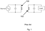
- FIG. 1 shows a conceptual representation of a resonant inductive power transmission system.
- a source of alternating electrical energy is applied to the primary inductor 100 of an air gap transformer.
- Magnetic coupling between the transformer primary inductor 100 and the transformer secondary inductor 102 transfers some proportion of the primary side energy to the transformer secondary inductor 102, which is removed by some distance from the primary inductor 100.
- the primary inductor magnetic field, the primary inductor current, and the secondary inductor current are proportional.
- Resonance applied to the primary inductor 100 increases primary side inductor current producing a corresponding increase in the magnetic flux, the secondary inductor current and the power transferred from the primary to the secondary.
- the magnetic flux from the primary inductor 100 induces a voltage into the winding of secondary inductor 102.
- Maximum secondary current and therefore maximum power transmission occurs when the secondary inductor winding is resonant as well.
- the result is a two-pole resonant circuit consisting of two magnetically coupled resonant circuits.
- the resonant circuits can be parallel resonant with the inductor and capacitor wired in parallel as shown in FIG. 1 , or they can be series wired and series resonant.
- the primary and secondary side resonances need not share the same form.
- Efficient resonant inductive wireless power transfer relies upon maintaining a high degree of resonance in both the primary source inductor and a secondary load inductor.
- transformer primary and secondary resonant frequencies are affected by many factors including manufacturing variation, component tolerance, primary-secondary separation distance, axial alignment, temperature and other factors. Efficient resonant inductive wireless power transfer therefore demands continuous, autonomous adjustment in order to maintain the required high degree of resonance.
- the primary winding may be located on or in a horizontal surface and the secondary coil may be attached to the bottom of the vehicle.
- Translational displacement or movement in either or both the x-axis (e . g ., frontto-back) and they- axis (e . g ., side-to-side) dimensions leads to a non-concentric alignment of the secondary and the primary windings. This may include translational misalignment due to, for example, improper or imprecise positioning of the secondary winding above the primary winding as well as vehicle motion.
- Planar misalignment between the primary and secondary windings may be seen when the secondary is mounted to the underside of a vehicle and the vehicle itself is not situated perfectly planar parallel to the surface of the pavement on or in which the primary is emplaced. Under such circumstances, the primary and secondary windings will be misadjusted for resonance and a correction must be made based on the encountered conditions peculiar to a single instance of the placement of a vehicle. When the vehicle moves and is again situated with respect to the same primary, or another primary is located in a new location, the planar alignment will almost certainly be imperfect. In each case, the resonance of the system may be adjusted accordingly.
- the primary and secondary may fall out of precise alignment due to external forces acting on the vehicle. These forces may act in combination to change the position of the secondary with respect to the primary in the x, y, and/or z axes, and it can be seen that the result may be some form of misalignment due to translational displacement. This may be seen in a skew or planar misalignment, and/or a vertical or translational motion or displacement.
- displacements may be seen as discrete long-duration displacements, or as short duration movements, or as oscillatory motion.
- Mechanical displacement or motion disrupts resonant inductive power transfer resulting in reduced power transfer efficiency and engenders the possibility of system malfunction, shutdown or even system damage. For this reason automatic resonant adjustment or compensation may be a part of an exemplary embodiment of the invention.
- an embodiment of the invention may be responsive to the widest possible range of vehicle motions that would disturb a tuned resonant inductive transformer and to be able to make required adjustments quickly to effectively eliminate the deleterious effects of vibration and movement.
- the primary and secondary inductors along with their associated resonating components form a complex and interacting second order resonant network. Alteration, deviation or variation of any network component or parameter may result in less than optimum performance. Electrical components can be fabricated with a high degree of repeatability but the required high degree of manufacturing precision incurs undesirable development and manufacturing costs. The ability to absorb or otherwise compensate for manufacturing variability is therefore desirable in an exemplary embodiment of the invention.
- an embodiment of the invention may accommodate system variations arising between systems designed, manufactured, and installed by multiple companies and agencies.
- any primary side inductor and associated components designed and manufactured by any one company may be required to function automatically and/or flawlessly with any secondary side inductor and associated secondary side components manufactured by any other manufacturer.
- Such "mismatched" inductive power systems even if unified under an international standard, will face significant interoperability challenges. It is only through active and automatic re-tuning that these units can be caused to work efficiently.
- an exemplary embodiment of the invention includes resonance confirmation and likely resonance readjustment prior to each recharging event as well as continuous resonance monitoring and re-adjustment if necessary during the recharging operation. Incremental improvements over years of manufacture may result in variability in coil design that cannot be predicted. Automatic re-tuning offers a means to assure that legacy inductors continue to operate with newly designed and recently manufactured inductors.
- inductors of differing geometry it is possible for inductors of differing geometry to interoperate. This may be needed when a primary coil is larger or has a different morphology than the secondary coil. For example, an oval primary coil will need to operate with secondary coils of various size and shape. Again, automatic resonance adjustment may be necessary to establish and maintain resonance.
- Ambient temperature variations may also affect resonant tuning and require adjustment in an embodiment of the invention.
- Expected ambient operating temperatures vary widely due to geographic location, season, time of day, weather, wind, solar exposure, or shadow including the shadow of the charging vehicle.
- the secondary coil and associated electronics is further subject to vehicle thermal emissions, which might well dominate other thermal effects.
- large ambient temperature changes during charging cannot be discounted and vehicle side temperatures cannot be assumed to be the same as or to follow temperature of the ground mounted primary side coil.
- Coil resonance may vary with temperature due to thermal expansion and contraction of the coil itself, the temperature sensitivity of associated electronics components especially the resonating capacitors, changes in the magnetic permittivity of the associated ferrite material and also due to changes in coil separation distance induced by the temperature sensitivity of the vehicle tires and suspension components.
- the present invention provides a means of electronic tuning that makes the primary-secondary system of inductors readily adaptable to the dynamic charging of moving vehicles.
- the secondary inductor is fixed to the vehicle.
- a moving vehicle is caused to pass over a linear array of multiple independent primary inductors, with each primary inductor sequenced by an automatic sequencer to power on and then off in such a fashion as to couple power to the secondary vehicle inductor for a short interval of time as the vehicle passes overhead.
- the optimal x, y, z and parallel plane alignment conditions are achieved only momentarily for each primary-secondary coil combination.
- the present invention enables the practice of highly efficient bidirectional operation of power transmission where power can flow in either direction between the vehicle and an off-board device.
- power can flow in either direction between the vehicle and an off-board device.
- One or more of the above factors requiring active and automatic resonance control in vehicle mounted wireless power systems may be present in non-vehicular wireless power transfer applications and might well be accompanied by further, application and situation specific disturbing factors needing automated detection and correction.
- an exemplary embodiment of the invention may meet one or more of the following performance criteria:
- the means by which automatic re-tuning occurs must be in near-real-time and be continuous during the power transmission period.
- the technology used to accomplish re-tuning cannot be excessively massive or volumetrically large.
- the technology used to accomplish re-tuning should not demand a large power supply to operate or substantially depreciate the power transmission efficiency of the system.
- the technology used to accomplish re-tuning should not cause or produce secondary effects which degrade the other aspects of the inductive wireless power transfer performance.
- the technology used to accomplish this re-tuning should be tightly integrated into the electronic system of components to reduce overall system complexity, reduce cost, and improve the capacity of maintenance personnel to effectuate cures to malfunctioning inductive power systems.
- the technology used to accomplish re-tuning should represent only a small fraction of the cost of fabricating an inductive power system.
- the load side (secondary) inductor circuit resonance is allowed to vary according to one or more of the factors mentioned above.
- the load inductor resonance error polarity and magnitude may be determined by comparing the phase of the load inductor resonant circuit voltage waveform and the phase of the load resonant circuit current waveform.
- a wireless communications link from the secondary side to the primary side may indicate the magnitude and polarity of the secondary side resonance error and the primary side microcontroller may then adjust the frequency of the primary inductor excitation until secondary resonance is achieved, as indicated by secondary side voltage and current waveforms being in phase.
- the system operating frequency is adjusted such that the fixed tuned secondary resonator is always operated at its resonant frequency.
- primary side resonance may then be established at the newly adjusted operating frequency by adjustment or other manipulation of the primary side inductor and associated resonating and impedance matching components. What remains then is the adjustment of the primary side inductor and associated resonating components such that they are also resonant at the secondary side resonant operating frequency.
- Such resonance adjustment may be done by mechanically or electrically switching various reactances (such as, for example, capacitance) into or out of the circuit until resonance is achieved.
- An exemplary embodiment relies upon N switches and N capacitors, the later selected according to a binary 1-2-4-8 sequence which allows 2N evenly spaced reactance values from N switched reactances.
- multiple inductors can be switched into or out of the circuit as required or inductor taps can be switch selected as required.
- Resonant wireless power transfer requires a high degree of precision that may not be possible with a switched reactance approach using a practical number of switches and reactive components.
- the adjustment granularity achieved with a practical number of switches may be too large.
- Another exemplary embodiment not being part of the present invention may use an electrically variable reactance such as a varactor diode (voltage variable capacitor), or a current variable inductance in which a variable de bias current usually placed in a secondary control coil alters the permeability of a ferromagnetic core thereby altering the inductance.
- an electrically variable reactance such as a varactor diode (voltage variable capacitor), or a current variable inductance in which a variable de bias current usually placed in a secondary control coil alters the permeability of a ferromagnetic core thereby altering the inductance.
- the varactor diode may be unable to handle power levels in excess of a few milliwatts and cannot easily provide large capacitance values.
- the current variable inductor is large, heavy, and also may be unable to handle large power levels because the de bias current functions by moving the operational point of the magnetic core material towards saturation thereby reducing the inductor current and power rating.
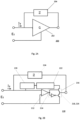
- FIG. 2A which shows a Miller reactance generator 200 comprising a conventional ideal voltage amplifier 202 with gain G and a feedback impedance Z 204. Input voltage and current to this network is indicated by ET and h, respectively.
- the voltage across the impedance Z is set by the amplifier voltage gain G which in turn affects the input terminal current h.
- G can be positive or negative, which allows negative (for G > +1) or positive (for G ⁇ +1) effective impedance values to be generated. It is noted that negative impedances are potentially unstable. Nevertheless, useful reactance adjustments may be possible using negative impedances operating with sufficient stability margins.
- amplifier gain G is a vector Z eff can also be altered by changing the amplifier phase shift.
- a disadvantage in the Miller Impedance Multiplier in FIG. 2A is the power requirement of the linear voltage amplifier 202.
- the percentage of total drive power provided by the voltage amplifier 202 is about the same as the desired adjustment range; a ten percent adjustment range means the voltage amplifier 202 provides about 10% of the total power. This may be a problem as the efficiency of an analog linear amplifier can be 20% or less. Consequently, semiconductor devices in the voltage amplifier 202 must be substantially oversized adding to the cost of such an implementation.
- Associated power supply and heat sink or heat management systems further inflate the cost of implementation.
- PWM pulse width modulation
- analog to PWM conversion block Such amplifiers are capable of very good efficiency; however, the PWM power switching devices may switch at frequencies much higher than the frequency of the signal to be amplified in order to satisfy the Nyquist criteria. Furthermore, precise amplitude or gain adjustment in a conventional PWM amplifier requires precise, fine grained adjustment of pulse width which places additional demands on the bandwidth of the PWM power switching devices. Thus, the power conversion efficiency of a conventional PWM amplifier implementation may require a fast PWM power switching devices, a requirement that carries cost and other practical liabilities.
- a method of circumventing the excessive bandwidth requirements imposed by conventional PWM amplifiers used as part of an electronically adjustable reactance generator can be developed from the principles that (1) the voltage and current waves in a resonant circuit of sufficiently high quality factor Q are sinusoidal and (2) that any sinusoid can be completely and absolutely described by three parameters: frequency, phase and amplitude.
- FIG. 2B shows an exemplary electronic reactance generator 210, according to an embodiment of the invention.
- a voltage comparator 212 samples the applied sinusoidal voltage waveform E T creating a square wave at point 214 that retains the frequency and the phase of the applied sinusoidal voltage waveform E T .
- the resulting square wave, output at point 214 controls the switching frequency and phase of a power switching circuit 216.
- An exemplary power switching circuit 216 is depicted in FIG. 2B as a half-bridge circuit comprising two power field effect transistors 218, 226. Other power switching circuits 216 may be used as well.
- the power switching circuit may comprises a full-bridge configuration, a flyback configuration, a resonant tank with single ended or push-pull drive configuration, a single or double ended forward converter configuration, or other power switching or power conversation circuit topologies of these general configurations.
- the output of the power switching circuit 216 may be a square wave with amplitude determined by the adjustable power supply 222.
- the adjustable power supply 222 may be a controlled voltage source thereby creating a half-bridge output voltage square-wave with controlled amplitude, or the adjustable power supply 222 may be implemented as a controlled current source thereby leading to a current square-wave at the half-bridge output. In either case, the square-wave retains the frequency and phase of the applied sinusoidal voltage E T .
- the missing E T amplitude parameter may be introduced by means of the Amplitude Detection block 220 which controls the amplitude of the adjustable power supply 222.
- the method of control can be analog, digital, or some combination thereof.
- the adjustable power supply 222 may be implemented as a conventional switch mode power supply having output amplitude controlled by any of the switch mode power supply control methods well known in conventional art. Further, in an exemplary embodiment, the amplitude detection block 220 - controlled power supply 222 transfer function Out/In may be made equal to G in the original analog Miller reactance generator diagram of FIG. 2A .
- the circuit shown in FIG. 2B replicates the frequency, phase and G scaled amplitude of the applied sinusoid voltage E T with a square wave at the output of the half-bridge.
- the square wave is generated, in part, by adjustable power supply 222, which is controlled, for example, by an exemplary switch mode power supply control method that avoids the power conversion inefficiencies of conventional analog amplifiers. Conversion of the square wave to a sinusoid is accomplished by the combined filtering action of the Thevenin impedance Z 224 and the LC resonant air core transfer transformer (not shown).
- Thevenin impedance Z 224 may be implemented as a pure reactance since a resistive component of the Thevenin impedance, if present, may introduce losses.
- the optimal reactance depends largely upon the half-bridge power supply source type.
- An inductive reactance may be preferred in conjunction with a voltage source fed power switch, while a capacitive reactance may be preferred when a current source power supply is used.
- the embodiment described above represents a general design methodology that may be implemented in multiple configurations. Accordingly, several alternative implementations of the electronic reactance generator are described below.
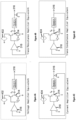
- FIG. 3 illustrates exemplary embodiments of an electronic reactance generator using the principles described above.
- This circuit includes a power generating section 300 and a reactance generating section 302 of the primary inductor side and a resonant air gap transfer transformer 304 and a rectifier-filter-load circuit 306 of the secondary inductor side.
- the power generator section 300 may contain a power switching circuit 308 that converts the dc power supply voltage V cc1 into a high power square-wave 310 that is applied through a DC blocking capacitor C b and Thevenin inductor L th to the primary side resonant LC circuit including resonating capacitor C r and primary inductor L p .
- the power generator 300 may see a purely resistive load, and as a result, the power generator 300 provides only real power.
- Square-wave harmonics may see a high impedance load established by the Thevenin inductor. For this reason square wave harmonic currents may be minimized.
- the exemplary reactance generator 302 may have the same topology as the real power generator 300.
- the reactance generator 302 may also develop a square wave 312 at its half-bridge output node 314. However, this square-wave 312 may or may not have the same phase or the same amplitude as the power generator square-wave 310.
- the phase and amplitude differences can be arranged to produce a current through the reactance generator's Thevenin inductor L th into the reactance summing node 316 that replicates the effect of a shunt, passive, and/or reactive component.
- the effective impedance of this virtual component may be easily altered by adjustment of the reactance generator's half-bridge drive phase and/or the half-bridge dc power supply magnitude.
- the voltage amplifier functionality of the Miller reactance generator shown in FIG. 3 may be implemented with a voltage comparator 318, an inverter and a half-bridge pair of power semiconductor switches.
- these semiconductor devices are shown as Field Effect Transistors (FETs) but other power switching devices such as but not limited to bipolar transistors, Insulated Gate Bipolar Transistors (IGBTs), or even vacuum tubes, or photo-conductive switches (e.g., laser activated photo-conductive switches) can be used.
- FETs Field Effect Transistors
- IGBTs Insulated Gate Bipolar Transistors
- photo-conductive switches e.g., laser activated photo-conductive switches
- the analog power amplifier is replaced with a simpler, less expensive, more efficient switching implementation.
- the voltage comparator 318 samples the voltage waveform at the reactance-summing node 316 and creates a square wave on-off representation of the summing node voltage.
- the amplitude information of the summing node sinusoidal waveform is obviously lost in this operation. It may be added back later.
- the square wave represents only the phase of the sinusoidal waveform that appears across the resonant circuit to be adjusted.
- the square wave and an inverted version of the square wave control two FET devices wired in a half-bridge or totem pole configuration and operated as switches instead of linear devices.
- the two FETs may generate a high power square wave 312 at their common node, the amplitude of which may be set by the magnitude of the half-bridge controllable power supply labeled V cc2 , which may be in turn applied to blocking capacitor C b and then Thevenin inductor L th .
- V cc2 changes the apparent gain of this unconventional Miller amplifier thereby changing the magnitude of the reactance generated by the Miller reactance generator.
- V cc2 is supplied by a digital or analog control of a switch- mode power supply (not shown).
- the control signal may be derived by a microcontroller (not shown) using a digital representation of the reactance summing node voltage.
- the microcontroller may adjust the magnitude of V cc2 in proportion to the amplitude of the sine wave present at the reactance-summing node.
- the constant of proportionality may be 1/(1-G) as before to produce the desired reactance.
- the Miller impedance in this embodiment which employs a half-bridge transistor pair fed by a controlled voltage source, is an inductor, which acts in part as a low pass filter thereby avoiding large current switching transients associated with the higher Fourier square wave components of the drive circuit. For this reason, only the fundamental component of the Miller drive waveform affects the primary resonant frequency as the harmonics are largely rejected. Also, the current waveform injected in the reactance summing node is essentially sinusoidal just as it is in the linear Miller reactance generator shown in FIG. 3 .
- the resonant transfer transformer 304 further includes a secondary inductor L s and a resonating capacitor C r .
- Rectifier-Filter circuit 320 rectifies and filters the received sinusoidal signal before applying it to load 322.
- alternative amplifier configurations may be incorporated into the reactance generator depicted in FIG. 3 .
- the alternative embodiments may be characterized according to the amplifier type and power switching topology selected. According to Table 1, the alternative amplifier embodiments include the voltage amplifier, the trans-conductance amplifier, the current amplifier and the trans-resistance amplifier. FIGS. 4A-4D depicts four such alternative amplifier configurations while Table 1 lists the gain definition for each.
- a composite voltage amplifier is implemented by sampling the reactance summing node voltage waveform with a voltage comparator 318 and using the resulting square-wave to control the transistor switches of the half-bridge with the half-bridge powered by a magnitude controlled voltage source.
- the voltage comparator 318 generates a square wave having the same frequency and phase as the sinusoidal signal at node 316 that drives a power switch powered by an adjustable voltage source 402.
- the voltage of the adjustable voltage source 402 is set to be proportional to the amplitude of the voltage sine wave present at the reactance summing node 316.
- the reactance-summing node voltage waveform is sampled with the voltage comparator 318 as before but using the resulting square-wave to control a half-bridge powered by an adjustable current source 404 effectively produces a composite trans-conductance amplifier implementation.
- a trans-conductance amplifier samples the voltage waveform present at the reactance summing node 316 and generates a square wave of the same frequency and phase that drives a power switch powered by an adjustable current source 404.
- the magnitude of the adjustable current source is set to be proportional to the amplitude of the current sine wave flowing into the reactance summing node 316.
- sampling the sinusoidal current present in the resonant circuit to be adjusted and using that square wave representation to drive a voltage source powered and current source powered Half-bridge respectively produces composite Trans-resistance and composite Current amplifier implementations.
- a current amplifier ( Figure 4C ) samples the current waveform flowing into the reactance summing node 316, generates a square wave of the same frequency and phase that drives a power switch powered by an adjustable current source 404.
- the magnitude of the adjustable current source 404 is set to be proportional to the amplitude of the current sine wave flowing into the reactance summing node 316.
- a composite trans-resistance amplifier ( Figure 4B ) samples the current waveform flowing into the reactance summing node 316, generates a square wave of the same frequency and phase that drives a power switch powered by an adjustable voltage source 402.
- the voltage of the adjustable voltage source 402 is set to be proportional to the current sine wave flowing into the reactance summing node 316.
- Amplifiers implemented with current source powered power switches are generally favored because of their tolerance to switching device simultaneous conduction commonly known as blow through and other faults that cause momentary, short circuit type faults.
- use of an inductor feedback reactance is favorable in embodiments using constant voltage powered switches, while a capacitive Miller generator feedback reactance is favorable in embodiments using constant current power switches.
- the most desirable amplifier configuration may depend upon the nature of the resonant load circuit, whether series or parallel resonance, the Miller Impedance type, whether inductive or capacitive and/or on other design factors.
- the half-bridge controllable power sources, a controllable voltage source, or a controllable current source as described above and represented in FIGS. 3 and 4A-4B can be replaced by voltage or current sources of fixed magnitude.
- Effective amplifier gain G and therefore the reactance proportionality factor 1/(1-G) may then implemented by pulse width modulation of the half-bridge.
- further reactance generator control techniques make use of the phase portion of the amplifier vector gain definition G.
- Z in Equation 1 is implemented as an ideal reactance, specifically an inductor or capacitor then Z eff may also be a pure reactance and the Miller Reactance generator may provide only imaginary power, VARs to the reactance summing node.
- Equation 1 implementing Z in Equation 1 as an ideal reactance but shifting the phase of the drive signal creates an imaginary component in the denominator of Equation 1 thereby making Z eff complex as well.
- the reactance generator may be providing (or absorbing) real power (Watts) in addition to reactive power (VARs) to the reactance-summing node.
- An exemplary embodiment of the invention arranges the magnitude and phase of G in the denominator of Equation 1 such that Z eff consists of the sum of a real negative resistance and an imaginary reactance either positive or negative in sign. In this way, the Miller Reactance generator shoulders part of the burden in providing real power to the lead.
- Control of drive signal phase allows the power handling capability of the Miller reactance generator half-bridge to be assigned to the generation of purely reactive power (VARS), purely real power (watts), or some combination of both, as desired, allowing it to provide more reactive power or more real power as desired.
- VARS purely reactive power
- watts purely real power
- the use of the electronically variable Miller reactance described above does not preclude the use of switched, tapped, or otherwise variable reactive elements. Indeed, switched reactive elements can be incorporated into a Miller variable reactance to provide coarse step reactance change with the Miller variable reactance relied upon to continuous fine adjustment.
- the square wave signal driving the Miller Reactance generator is derived from a sample of the sinusoidal voltage or current present at the reactance-summing node 316.
- this signal can be derived from the square wave that drives the main power half-bridge either in phase or in quadrature.
- the reactance generator clock may be generated in a microcontroller or other digital or software controlled device.
- FIG. 3 depicts an exemplary embodiment having an asymmetrical resonance LC circuit, asymmetrical in the sense that one side is connected of the LC circuit is grounded and the LC resonance circuit is driven by a pair of half-bridge circuits both having an un-balanced output with respect to circuit ground.
- additional embodiments of the invention may employ balanced LC resonant circuits with neither side connected directly to ground driven by the balanced, symmetrical output of H-bridge drivers instead of half-bridge drivers.
- the power switching circuit of the invention may comprise a half-bridge configuration, a full-bridge configuration, a flyback configuration, a resonant tank with single ended or push-pull drive configuration, a single or double ended forward converter configuration, or other power switching or power conversation circuit topologies of these general configurations.
- Multiple power switching topologies apparent to people skilled in the art can be used in an embodiment of the power switching function of the switching amplifier portion of the Miller reactance generator described herein.
- the primary side and secondary side inductances of the transfer transformer must be resonated by connection of a resonating capacitor for efficient operation.
- the resonating capacitor can be connected in series creating a series resonant circuit, or it can be connected in parallel creating a parallel resonant circuit.
- the series resonant connection of the transfer transformer primary side inductance is well suited to be driven by power switching circuits powered by a voltage source, while the parallel resonant connection of the transfer transformer primary side inductance is well suited to be driven by power switching circuits powered by a current source.
- these broad design guidelines may be altered by the addition of an LC impedance matching network.
Landscapes
- Engineering & Computer Science (AREA)
- Power Engineering (AREA)
- Computer Networks & Wireless Communication (AREA)
- Inverter Devices (AREA)
- Current-Collector Devices For Electrically Propelled Vehicles (AREA)
- Networks Using Active Elements (AREA)
- Measurement Of Resistance Or Impedance (AREA)
- Radar Systems Or Details Thereof (AREA)
- Transmitters (AREA)
- Supply And Distribution Of Alternating Current (AREA)
- Amplifiers (AREA)
Claims (8)
- Générateur de réactance ajustable (210) pour un système de transfert de puissance inductrice résonante, comprenant :un comparateur (212) agencé pour recevoir une forme d'onde de tension sinusoïdale d'entrée et pour produire en sortie une première forme d'onde de tension à onde carrée qui maintient une fréquence et une phase de la forme d'onde sinusoïdale d'entrée ;un circuit commutateur de puissance (216) agencé pour recevoir ladite première forme d'onde de tension à onde carrée en tant que signal de commande et pour produire en sortie une seconde forme d'onde de tension à onde carrée (312) qui maintient la fréquence et la phase de la forme d'onde de tension sinusoïdale d'entrée ;un détecteur d'amplitude (220) agencé pour détecter une amplitude de la forme d'onde de tension sinusoïdale d'entrée ;une alimentation électrique ajustable (222) connectée au circuit commutateur de puissance (216) et agencée pour ajuster une amplitude de la seconde forme d'onde de tension à onde carrée (312) sur la base de l'amplitude détectée par le détecteur d'amplitude (220) ; etune impédance de Thévenin (224) et un transformateur de transfert à noyau d'air résonant LC agencé afin de convertir la seconde forme d'onde de tension à onde carrée ajustée en amplitude en une forme d'onde de tension sinusoïdale de sortie, dans lequel la conversion de la seconde forme d'onde de tension à onde carrée ajustée en amplitude en la forme d'onde de tension sinusoïdale de sortie fournit un effet d'une réactance ajustable ;dans lequel le générateur de réactance ajustable comprend en outre des moyens pour fournir ladite forme d'onde de tension sinusoïdale de sortie à une charge du système de transfert de puissance inductrice résonante.
- Générateur de réactance ajustable selon une quelconque revendication précédente, dans lequel la fréquence, la phase et l'amplitude de la forme d'onde sinusoïdale d'entrée sont dupliquées avec la seconde forme d'onde de tension à onde carrée ajustée en amplitude.
- Générateur de réactance ajustable selon une quelconque revendication précédente, dans lequel le circuit commutateur de puissance comprend un circuit en demi-pont comprenant deux dispositifs commutateurs de puissance.
- Générateur de réactance ajustable selon une quelconque revendication précédente, dans lequel le circuit commutateur de puissance comprend une configuration de pont complet, une configuration de retour, un réservoir résonant avec configuration d'excitation à sortie unique ou pousser-tirer, ou une configuration de convertisseur direct à sortie unique ou double.
- Générateur de réactance ajustable selon l'une quelconque des revendications 1 et 2, dans lequel l'alimentation électrique ajustable comprend une source de tension commandée ou une source de courant commandée.
- Générateur de réactance ajustable selon l'une quelconque des revendications 1 et 2, dans lequel l'alimentation électrique ajustable comprend une alimentation électrique à découpage.
- Procédé d'ajustement d'une réactance d'un générateur de réactance ajustable (210) pour un système de transfert de puissance inductrice résonante selon l'une quelconque des revendications 1 à 6, comprenant :la génération, à partir d'une forme d'onde de tension sinusoïdale d'entrée, d'une première forme d'onde de tension à onde carrée qui maintient une fréquence et une phase de la forme d'onde de tension sinusoïdale d'entrée ;l'application de ladite première forme d'onde de tension à onde carrée en tant que signal de commande sur un circuit commutateur de puissance (216), moyennant quoi ledit circuit commutateur de puissance produit en sortie une seconde forme d'onde de tension à onde carrée (312) qui maintient la fréquence et la phase de la forme d'onde de tension sinusoïdale d'entrée ;l'ajustement d'une amplitude de la seconde forme d'onde de tension à onde carrée (312) sur la base de l'amplitude de la forme d'onde de tension sinusoïdale d'entrée détectée par un détecteur d'amplitude (220) ;la conversion de la seconde forme d'onde de tension à onde carrée ajustée en amplitude en une forme d'onde de tension sinusoïdale de sortie ayant un effet d'une réactance ajustable ; etla fourniture de ladite forme d'onde de tension sinusoïdale de sortie à une charge d'un système de transfert de puissance inductrice résonante.
- Procédé selon la revendication 7, dans lequel la fréquence, la phase et l'amplitude de la forme d'onde de tension sinusoïdale d'entrée sont dupliquées avec la seconde forme d'onde de tension à onde carrée ajustée en amplitude.
Applications Claiming Priority (3)
| Application Number | Priority Date | Filing Date | Title |
|---|---|---|---|
| US201261645850P | 2012-05-11 | 2012-05-11 | |
| PCT/US2013/040581 WO2013170173A2 (fr) | 2012-05-11 | 2013-05-10 | Procédé et appareil de génération de réactance réglable |
| EP13787746.0A EP2847771B1 (fr) | 2012-05-11 | 2013-05-10 | Système de transmission d'énergie sans fil par couplage inductif à résonance avec une réactance variable |
Related Parent Applications (1)
| Application Number | Title | Priority Date | Filing Date |
|---|---|---|---|
| EP13787746.0A Division EP2847771B1 (fr) | 2012-05-11 | 2013-05-10 | Système de transmission d'énergie sans fil par couplage inductif à résonance avec une réactance variable |
Publications (2)
| Publication Number | Publication Date |
|---|---|
| EP3309928A1 EP3309928A1 (fr) | 2018-04-18 |
| EP3309928B1 true EP3309928B1 (fr) | 2023-05-17 |
Family
ID=49548089
Family Applications (2)
| Application Number | Title | Priority Date | Filing Date |
|---|---|---|---|
| EP17204148.5A Active EP3309928B1 (fr) | 2012-05-11 | 2013-05-10 | Système de transmission d'énergie à couplage inductif par résonance avec une réactance ajustable |
| EP13787746.0A Active EP2847771B1 (fr) | 2012-05-11 | 2013-05-10 | Système de transmission d'énergie sans fil par couplage inductif à résonance avec une réactance variable |
Family Applications After (1)
| Application Number | Title | Priority Date | Filing Date |
|---|---|---|---|
| EP13787746.0A Active EP2847771B1 (fr) | 2012-05-11 | 2013-05-10 | Système de transmission d'énergie sans fil par couplage inductif à résonance avec une réactance variable |
Country Status (10)
| Country | Link |
|---|---|
| US (2) | US9754717B2 (fr) |
| EP (2) | EP3309928B1 (fr) |
| JP (1) | JP6290864B2 (fr) |
| KR (1) | KR101914820B1 (fr) |
| CN (2) | CN104508768B (fr) |
| CA (1) | CA2873195C (fr) |
| ES (2) | ES2661374T3 (fr) |
| MX (2) | MX350033B (fr) |
| PT (2) | PT2847771T (fr) |
| WO (1) | WO2013170173A2 (fr) |
Families Citing this family (47)
| Publication number | Priority date | Publication date | Assignee | Title |
|---|---|---|---|---|
| US11214164B2 (en) * | 2008-06-01 | 2022-01-04 | Hyundai Motor Company | Method and apparatus for controlling wireless power transfer to electric vehicle using bridgeless rectifier |
| US9391461B2 (en) * | 2011-05-31 | 2016-07-12 | Samsung Electronics Co., Ltd. | Wireless power transmission and charging system, and power control method of wireless power transmission and charging system |
| PT2847771T (pt) | 2012-05-11 | 2018-03-01 | Momentum Dynamics Corp | Sistema de transmissão de potência indutiva ressonante com reatância ajustável |
| EP2868919A1 (fr) * | 2013-11-05 | 2015-05-06 | Openhydro IP Limited | Système et procédé de protection de turbulence pour des générateurs de turbine |
| US9673784B2 (en) | 2013-11-21 | 2017-06-06 | Apple Inc. | Using pulsed biases to represent DC bias for charging |
| EP3074988A4 (fr) * | 2013-11-27 | 2017-07-12 | Momentum Dynamics Corporation | Transmission sans fil à fréquence de secteur et à tension de secteur |
| CN104734511A (zh) * | 2013-12-20 | 2015-06-24 | 通用电气公司 | 空芯变压器、隔离式无磁开关电源及磁共振成像系统 |
| US9537353B1 (en) | 2014-06-03 | 2017-01-03 | Apple Inc. | Methods for detecting mated coils |
| US9685814B1 (en) | 2014-06-13 | 2017-06-20 | Apple Inc. | Detection of coil coupling in an inductive charging system |
| US10014733B2 (en) | 2014-08-28 | 2018-07-03 | Apple Inc. | Temperature management in a wireless energy transfer system |
| US10193372B2 (en) | 2014-09-02 | 2019-01-29 | Apple Inc. | Operating an inductive energy transfer system |
| US9496707B2 (en) * | 2014-12-22 | 2016-11-15 | Schweitzer Engineering Laboratories, Inc. | Generator protection element |
| CN105871213B (zh) * | 2015-01-21 | 2020-02-21 | 南京航空航天大学 | 一种非接触电能传输系统中的控制方法和装置 |
| CA2982928A1 (fr) | 2015-04-20 | 2016-10-27 | Tolero Pharmaceuticals, Inc. | Prediction de la reaction a l'alvocidib par identification de profil mitochondrial |
| US10666084B2 (en) | 2015-07-10 | 2020-05-26 | Apple Inc. | Detection and notification of an unpowered releasable charging device |
| CN105226839B (zh) * | 2015-11-12 | 2018-06-08 | 中国人民解放军国防科学技术大学 | 磁耦合谐振式无线电能传输系统及其双侧自调谐方法 |
| WO2018048312A1 (fr) | 2016-09-06 | 2018-03-15 | Powerbyproxi Limited | Émetteur de puissance inductive |
| US10644531B1 (en) | 2016-09-22 | 2020-05-05 | Apple Inc. | Adaptable power rectifier for wireless charger system |
| US10601250B1 (en) * | 2016-09-22 | 2020-03-24 | Apple Inc. | Asymmetric duty control of a half bridge power converter |
| JP6690609B2 (ja) * | 2017-04-06 | 2020-04-28 | 株式会社村田製作所 | 磁界発生回路 |
| US10389274B2 (en) * | 2017-04-07 | 2019-08-20 | Apple Inc. | Boosted output inverter for electronic devices |
| US10523063B2 (en) | 2017-04-07 | 2019-12-31 | Apple Inc. | Common mode noise compensation in wireless power systems |
| US11087913B2 (en) | 2017-05-15 | 2021-08-10 | General Electric Company | Transformer system |
| DE102017113425A1 (de) * | 2017-06-19 | 2018-12-20 | Otto-Von-Guericke-Universität Magdeburg | Vorrichtung und Verfahren zur aktiven Erzeugung und Einprägung von Blindleistung in induktive Übertragungssysteme |
| US10931097B2 (en) | 2017-09-25 | 2021-02-23 | Schweitzer Engineering Laboratories, Inc. | Generator stator ground protection using third harmonic |
| US10333291B2 (en) | 2017-09-25 | 2019-06-25 | Schweitzer Engineering Laboratories, Inc. | Multiple generator ground fault detection |
| JP7344199B2 (ja) * | 2017-10-05 | 2023-09-13 | フィリップ・モーリス・プロダクツ・ソシエテ・アノニム | 連続的な電力調整を有する電気的に作動するエアロゾル発生装置 |
| DE102017218066A1 (de) | 2017-10-11 | 2019-04-11 | Bayerische Motoren Werke Aktiengesellschaft | Primäreinheit für ein induktives Ladesystem, sowie Verfahren zum Betrieb einer Primäreinheit |
| US10469778B2 (en) * | 2017-10-27 | 2019-11-05 | Semiconductor Components Industries, Llc | Methods and apparatus for actuator control |
| CN107799110B (zh) * | 2017-11-01 | 2020-11-20 | 南昌航空大学 | 一种扫频式赫姆霍兹消声器 |
| DE102017220991B4 (de) * | 2017-11-23 | 2022-10-06 | Siemens Healthcare Gmbh | Transformatoreinheit sowie Verfahren zum Betrieb einer Transformatoreinheit |
| WO2019133803A1 (fr) * | 2017-12-29 | 2019-07-04 | The Trustees Of Princeton University | Système et procédé pour réseau de direction à réactance (rsn) |
| CN109045468B (zh) * | 2018-08-09 | 2022-05-24 | 西安科悦医疗技术有限公司 | 一种耳部迷走神经刺激系统及其装置 |
| US10797632B2 (en) | 2018-08-21 | 2020-10-06 | Schweitzer Engineering Laboratories, Inc. | Sensitive directional element for generator protection |
| CN110046370A (zh) * | 2018-12-17 | 2019-07-23 | 上海航天电子有限公司 | 一种应用数值场求解折叠波导结构特性阻抗的方法 |
| CN109755006A (zh) * | 2019-01-28 | 2019-05-14 | 华南理工大学 | 一种基于pt对称原理的并联-并联型无铁芯变压器 |
| CN109981082B (zh) * | 2019-04-30 | 2023-09-12 | 中国工程物理研究院流体物理研究所 | 一种基于光导开关的核电磁脉冲模拟器脉冲源 |
| US10819261B1 (en) | 2019-10-25 | 2020-10-27 | Schweitzer Engineering Laboratories, Inc. | Security improvements for electric power generator protection |
| US11538614B2 (en) | 2019-11-20 | 2022-12-27 | General Electric Technology Gmbh | Flexible transformer system |
| JP2022016299A (ja) * | 2020-07-10 | 2022-01-21 | 島田理化工業株式会社 | 非接触給電用インバータ装置、非接触給電用インバータ装置の制御方法、非接触送電装置、非接触送受電装置、非接触給電システムならびに非接触送受電システム |
| JP2023540278A (ja) * | 2020-08-27 | 2023-09-22 | エーテルダイン テクノロジーズ インコーポレイテッド | 連続可変能動リアクタンスシステム及び方法 |
| EP3961899B1 (fr) * | 2020-08-31 | 2023-11-22 | STMicroelectronics S.r.l. | Estimation du facteur de qualité d'un élément inductif |
| US20230420991A1 (en) * | 2020-11-04 | 2023-12-28 | Intdevice Limited | Improvements relating to wireless power transfer |
| US11631972B2 (en) | 2020-12-16 | 2023-04-18 | Schweitzer Engineering Laboratories, Inc. | Accurate modeling of equipment overexcitation damage curves |
| CN113972755B (zh) * | 2021-11-19 | 2023-08-11 | 宁波道充科技有限公司 | 可自动关断的无线充电原边线圈的补偿结构 |
| CN115040938B (zh) * | 2022-06-06 | 2023-12-15 | 河北光兴半导体技术有限公司 | 一种除尘装置 |
| US11946966B1 (en) | 2023-02-20 | 2024-04-02 | Schweitzer Engineering Laboratories, Inc. | Selective stator ground fault protection using positive-sequence voltage reference |
Family Cites Families (24)
| Publication number | Priority date | Publication date | Assignee | Title |
|---|---|---|---|---|
| US3539826A (en) | 1967-09-01 | 1970-11-10 | Ibm | Active variable impedance device for large signal applications |
| JPS5947495B2 (ja) * | 1975-04-04 | 1984-11-19 | 株式会社日立製作所 | 可変インピ−ダンス回路 |
| US4002058A (en) * | 1976-03-03 | 1977-01-11 | General Electric Company | Method and apparatus for vibration of a specimen by controlled electromagnetic force |
| CH652215A5 (de) * | 1981-05-18 | 1985-10-31 | Novasina Ag | Verfahren und schaltungsanordnung zur messung der impedanz eines sensors. |
| US5258766A (en) | 1987-12-10 | 1993-11-02 | Uniscan Ltd. | Antenna structure for providing a uniform field |
| CN87216457U (zh) * | 1987-12-17 | 1988-08-17 | 山西省机械设计研究所 | 可调式电流互感器负载箱 |
| ZA892468B (en) * | 1988-04-11 | 1989-12-27 | Uniscan Ltd | Improvements in or relating to cutting elements foactuator and communication system r rotary drill bits |
| US5041763A (en) | 1989-12-22 | 1991-08-20 | Lutron Electronics Co., Inc. | Circuit and method for improved dimming of gas discharge lamps |
| JPH0878252A (ja) * | 1994-09-08 | 1996-03-22 | Otsuka Sci Kk | 共振型空心変圧器 |
| DE19515510A1 (de) | 1995-04-27 | 1997-02-20 | Patent Treuhand Ges Fuer Elektrische Gluehlampen Mbh | Schaltungsanordnung zum Impulsbetrieb von Entladungslampen |
| JPH09149565A (ja) * | 1995-09-22 | 1997-06-06 | Hitachi Maxell Ltd | 非接触転送電源装置 |
| US6442434B1 (en) * | 1999-10-19 | 2002-08-27 | Abiomed, Inc. | Methods and apparatus for providing a sufficiently stable power to a load in an energy transfer system |
| CN201061162Y (zh) * | 2007-05-13 | 2008-05-14 | 德赛电子(惠州)有限公司 | 一种信号转换电路 |
| US8364099B2 (en) | 2007-07-05 | 2013-01-29 | Panasonic Corporation | Methods and apparatus for controlling leakage and power dissipation in radio frequency power amplifiers |
| US8855554B2 (en) | 2008-03-05 | 2014-10-07 | Qualcomm Incorporated | Packaging and details of a wireless power device |
| JP2009268181A (ja) * | 2008-04-22 | 2009-11-12 | Olympus Corp | エネルギー供給装置 |
| CN101388610B (zh) * | 2008-07-08 | 2010-06-02 | 河北省电力研究院 | 一种有关全封闭组合电器中电压互感器谐振升压的方法 |
| US8532724B2 (en) * | 2008-09-17 | 2013-09-10 | Qualcomm Incorporated | Transmitters for wireless power transmission |
| JP2010183722A (ja) * | 2009-02-05 | 2010-08-19 | Mitsumi Electric Co Ltd | Dc−dcコンバータおよびスイッチング制御回路 |
| US20130049482A1 (en) * | 2009-09-28 | 2013-02-28 | Powermat Ltd. | System and method for regulating inductive power transmission |
| US8564370B2 (en) | 2010-05-20 | 2013-10-22 | Himax Analogic, Inc. | Error amplifier and LED circuit comprising the same |
| WO2012094306A1 (fr) * | 2011-01-04 | 2012-07-12 | Enphase Energy, Inc. | Procédé et appareil destinés à une conversion électronique de puissance résonnante |
| CN103947092B (zh) * | 2011-10-26 | 2017-02-08 | 美高森美公司 | 用于降压dc/dc转换器的滞后控制 |
| PT2847771T (pt) | 2012-05-11 | 2018-03-01 | Momentum Dynamics Corp | Sistema de transmissão de potência indutiva ressonante com reatância ajustável |
-
2013
- 2013-05-10 PT PT137877460T patent/PT2847771T/pt unknown
- 2013-05-10 WO PCT/US2013/040581 patent/WO2013170173A2/fr active Application Filing
- 2013-05-10 JP JP2015511763A patent/JP6290864B2/ja active Active
- 2013-05-10 MX MX2016011638A patent/MX350033B/es unknown
- 2013-05-10 ES ES13787746.0T patent/ES2661374T3/es active Active
- 2013-05-10 MX MX2014013715A patent/MX347755B/es active IP Right Grant
- 2013-05-10 ES ES17204148T patent/ES2951769T3/es active Active
- 2013-05-10 EP EP17204148.5A patent/EP3309928B1/fr active Active
- 2013-05-10 EP EP13787746.0A patent/EP2847771B1/fr active Active
- 2013-05-10 KR KR1020147034846A patent/KR101914820B1/ko active IP Right Grant
- 2013-05-10 CA CA2873195A patent/CA2873195C/fr active Active
- 2013-05-10 PT PT172041485T patent/PT3309928T/pt unknown
- 2013-05-10 CN CN201380032535.0A patent/CN104508768B/zh active Active
- 2013-05-10 US US13/891,917 patent/US9754717B2/en active Active
- 2013-05-10 CN CN201610662526.5A patent/CN106451575B/zh active Active
-
2017
- 2017-08-01 US US15/665,688 patent/US10319517B2/en active Active
Also Published As
| Publication number | Publication date |
|---|---|
| PT3309928T (pt) | 2023-08-17 |
| CN106451575A (zh) | 2017-02-22 |
| EP2847771A2 (fr) | 2015-03-18 |
| KR20150027086A (ko) | 2015-03-11 |
| WO2013170173A2 (fr) | 2013-11-14 |
| KR101914820B1 (ko) | 2018-11-02 |
| CA2873195A1 (fr) | 2013-11-14 |
| ES2951769T3 (es) | 2023-10-24 |
| WO2013170173A3 (fr) | 2013-12-27 |
| CN106451575B (zh) | 2019-04-02 |
| MX347755B (es) | 2017-05-10 |
| CA2873195C (fr) | 2020-09-22 |
| US20180053598A1 (en) | 2018-02-22 |
| US10319517B2 (en) | 2019-06-11 |
| US9754717B2 (en) | 2017-09-05 |
| JP2015516142A (ja) | 2015-06-04 |
| PT2847771T (pt) | 2018-03-01 |
| CN104508768B (zh) | 2017-08-08 |
| CN104508768A (zh) | 2015-04-08 |
| EP2847771B1 (fr) | 2017-11-29 |
| MX350033B (es) | 2017-08-23 |
| EP3309928A1 (fr) | 2018-04-18 |
| EP2847771A4 (fr) | 2016-06-01 |
| JP6290864B2 (ja) | 2018-03-07 |
| US20130300209A1 (en) | 2013-11-14 |
| ES2661374T3 (es) | 2018-03-28 |
| MX2014013715A (es) | 2015-08-10 |
Similar Documents
| Publication | Publication Date | Title |
|---|---|---|
| US10319517B2 (en) | Method of and apparatus for generating an adjustable reactance | |
| Colak et al. | A novel phase-shift control of semibridgeless active rectifier for wireless power transfer | |
| Aldhaher et al. | Tuning class E inverters applied in inductive links using saturable reactors | |
| CN106852182B (zh) | 具有固定调谐和功率限制的可变距离无线功率传输系统 | |
| US9246409B2 (en) | Method and apparatus for controlling LCL converters using asymmetric voltage cancellation techniques | |
| CN111279577A (zh) | 借助于自适应匹配网络的电容性无线电力传输 | |
| KR20210010673A (ko) | 무선 전력 전송 장치 | |
| Ishihara et al. | Autonomous system concept of multiple-receiver inductive coupling wireless power transfer for output power stabilization against cross-interference among receivers and resonance frequency tolerance | |
| US11817834B2 (en) | High frequency wireless power transfer system, transmitter, and receiver therefor | |
| Huang et al. | Load-Independent Push–Pull Class E $^ 2$ Topology With Coupled Inductors for MHz-WPT Applications | |
| Keeling et al. | Variable tuning in LCL compensated contactless power transfer pickups | |
| Ishihara et al. | Automatic active compensation method of cross-coupling in multiple-receiver resonant inductive coupling wireless power transfer systems | |
| US20180269726A1 (en) | Inductive Power Transmitter | |
| Asa et al. | A novel phase control of semi bridgeless active rectifier for wireless power transfer applications | |
| Rezazade et al. | A novel efficient hybrid compensation topology for wireless power transfer | |
| Prasad et al. | A novel dual-lcc hybrid compensation network for high-efficiency cc-cv wireless charging of an ev battery considering weak communication | |
| Baguley et al. | Theory and control of wireless power transfer systems | |
| Vishnu et al. | A phase shift control strategy for bidirectional power flow in capacitive wireless power transfer system using LCLC compensation | |
| Woronowicz et al. | A practical approach to inductive power transfer systems for transportation applications using boucherot bridge method | |
| US11843257B2 (en) | Power transmission apparatus and wireless power transmission system | |
| Liu et al. | A New Simplified Method and Design Guidelines for the Optimization of Push–Pull Class $\Phi _ {2} $ Converters for Wireless Power Transfer Applications | |
| JP7542013B2 (ja) | 電気負荷に電力を供給するためのコンバータ | |
| Li et al. | Advanced Wireless Power Conversion Technologies Topology, Modulation, and Control | |
| Huang et al. | Misalignment Tolerance of Electric Vehicle Wireless Charging System based on Multiple Decoupled Receiving Coils and Series Connected Diode Rectifiers | |
| WO2017131532A1 (fr) | Émetteur de puissance inductive |
Legal Events
| Date | Code | Title | Description |
|---|---|---|---|
| PUAI | Public reference made under article 153(3) epc to a published international application that has entered the european phase |
Free format text: ORIGINAL CODE: 0009012 |
|
| STAA | Information on the status of an ep patent application or granted ep patent |
Free format text: STATUS: THE APPLICATION HAS BEEN PUBLISHED |
|
| AC | Divisional application: reference to earlier application |
Ref document number: 2847771 Country of ref document: EP Kind code of ref document: P |
|
| AK | Designated contracting states |
Kind code of ref document: A1 Designated state(s): AL AT BE BG CH CY CZ DE DK EE ES FI FR GB GR HR HU IE IS IT LI LT LU LV MC MK MT NL NO PL PT RO RS SE SI SK SM TR |
|
| STAA | Information on the status of an ep patent application or granted ep patent |
Free format text: STATUS: REQUEST FOR EXAMINATION WAS MADE |
|
| 17P | Request for examination filed |
Effective date: 20181017 |
|
| RBV | Designated contracting states (corrected) |
Designated state(s): AL AT BE BG CH CY CZ DE DK EE ES FI FR GB GR HR HU IE IS IT LI LT LU LV MC MK MT NL NO PL PT RO RS SE SI SK SM TR |
|
| STAA | Information on the status of an ep patent application or granted ep patent |
Free format text: STATUS: REQUEST FOR EXAMINATION WAS MADE |
|
| STAA | Information on the status of an ep patent application or granted ep patent |
Free format text: STATUS: EXAMINATION IS IN PROGRESS |
|
| 17Q | First examination report despatched |
Effective date: 20210330 |
|
| GRAP | Despatch of communication of intention to grant a patent |
Free format text: ORIGINAL CODE: EPIDOSNIGR1 |
|
| STAA | Information on the status of an ep patent application or granted ep patent |
Free format text: STATUS: GRANT OF PATENT IS INTENDED |
|
| INTG | Intention to grant announced |
Effective date: 20211008 |
|
| GRAJ | Information related to disapproval of communication of intention to grant by the applicant or resumption of examination proceedings by the epo deleted |
Free format text: ORIGINAL CODE: EPIDOSDIGR1 |
|
| STAA | Information on the status of an ep patent application or granted ep patent |
Free format text: STATUS: EXAMINATION IS IN PROGRESS |
|
| INTC | Intention to grant announced (deleted) | ||
| GRAP | Despatch of communication of intention to grant a patent |
Free format text: ORIGINAL CODE: EPIDOSNIGR1 |
|
| STAA | Information on the status of an ep patent application or granted ep patent |
Free format text: STATUS: GRANT OF PATENT IS INTENDED |
|
| INTG | Intention to grant announced |
Effective date: 20221205 |
|
| RAP3 | Party data changed (applicant data changed or rights of an application transferred) |
Owner name: INDUCTEV INC. |
|
| GRAS | Grant fee paid |
Free format text: ORIGINAL CODE: EPIDOSNIGR3 |
|
| GRAA | (expected) grant |
Free format text: ORIGINAL CODE: 0009210 |
|
| STAA | Information on the status of an ep patent application or granted ep patent |
Free format text: STATUS: THE PATENT HAS BEEN GRANTED |
|
| RAP3 | Party data changed (applicant data changed or rights of an application transferred) |
Owner name: INDUCTEV INC. |
|
| AC | Divisional application: reference to earlier application |
Ref document number: 2847771 Country of ref document: EP Kind code of ref document: P |
|
| AK | Designated contracting states |
Kind code of ref document: B1 Designated state(s): AL AT BE BG CH CY CZ DE DK EE ES FI FR GB GR HR HU IE IS IT LI LT LU LV MC MK MT NL NO PL PT RO RS SE SI SK SM TR |
|
| REG | Reference to a national code |
Ref country code: GB Ref legal event code: FG4D |
|
| REG | Reference to a national code |
Ref country code: DE Ref legal event code: R096 Ref document number: 602013083812 Country of ref document: DE |
|
| REG | Reference to a national code |
Ref country code: CH Ref legal event code: EP |
|
| REG | Reference to a national code |
Ref country code: IE Ref legal event code: FG4D |
|
| REG | Reference to a national code |
Ref country code: AT Ref legal event code: REF Ref document number: 1568808 Country of ref document: AT Kind code of ref document: T Effective date: 20230615 |
|
| REG | Reference to a national code |
Ref country code: SE Ref legal event code: TRGR |
|
| REG | Reference to a national code |
Ref country code: PT Ref legal event code: SC4A Ref document number: 3309928 Country of ref document: PT Date of ref document: 20230817 Kind code of ref document: T Free format text: AVAILABILITY OF NATIONAL TRANSLATION Effective date: 20230802 |
|
| REG | Reference to a national code |
Ref country code: LT Ref legal event code: MG9D |
|
| REG | Reference to a national code |
Ref country code: NL Ref legal event code: MP Effective date: 20230517 |
|
| REG | Reference to a national code |
Ref country code: ES Ref legal event code: FG2A Ref document number: 2951769 Country of ref document: ES Kind code of ref document: T3 Effective date: 20231024 |
|
| PG25 | Lapsed in a contracting state [announced via postgrant information from national office to epo] |
Ref country code: NO Free format text: LAPSE BECAUSE OF FAILURE TO SUBMIT A TRANSLATION OF THE DESCRIPTION OR TO PAY THE FEE WITHIN THE PRESCRIBED TIME-LIMIT Effective date: 20230817 Ref country code: NL Free format text: LAPSE BECAUSE OF FAILURE TO SUBMIT A TRANSLATION OF THE DESCRIPTION OR TO PAY THE FEE WITHIN THE PRESCRIBED TIME-LIMIT Effective date: 20230517 |
|
| PG25 | Lapsed in a contracting state [announced via postgrant information from national office to epo] |
Ref country code: RS Free format text: LAPSE BECAUSE OF FAILURE TO SUBMIT A TRANSLATION OF THE DESCRIPTION OR TO PAY THE FEE WITHIN THE PRESCRIBED TIME-LIMIT Effective date: 20230517 Ref country code: PL Free format text: LAPSE BECAUSE OF FAILURE TO SUBMIT A TRANSLATION OF THE DESCRIPTION OR TO PAY THE FEE WITHIN THE PRESCRIBED TIME-LIMIT Effective date: 20230517 Ref country code: LV Free format text: LAPSE BECAUSE OF FAILURE TO SUBMIT A TRANSLATION OF THE DESCRIPTION OR TO PAY THE FEE WITHIN THE PRESCRIBED TIME-LIMIT Effective date: 20230517 Ref country code: LT Free format text: LAPSE BECAUSE OF FAILURE TO SUBMIT A TRANSLATION OF THE DESCRIPTION OR TO PAY THE FEE WITHIN THE PRESCRIBED TIME-LIMIT Effective date: 20230517 Ref country code: IS Free format text: LAPSE BECAUSE OF FAILURE TO SUBMIT A TRANSLATION OF THE DESCRIPTION OR TO PAY THE FEE WITHIN THE PRESCRIBED TIME-LIMIT Effective date: 20230917 Ref country code: HR Free format text: LAPSE BECAUSE OF FAILURE TO SUBMIT A TRANSLATION OF THE DESCRIPTION OR TO PAY THE FEE WITHIN THE PRESCRIBED TIME-LIMIT Effective date: 20230517 Ref country code: GR Free format text: LAPSE BECAUSE OF FAILURE TO SUBMIT A TRANSLATION OF THE DESCRIPTION OR TO PAY THE FEE WITHIN THE PRESCRIBED TIME-LIMIT Effective date: 20230818 |
|
| PG25 | Lapsed in a contracting state [announced via postgrant information from national office to epo] |
Ref country code: FI Free format text: LAPSE BECAUSE OF FAILURE TO SUBMIT A TRANSLATION OF THE DESCRIPTION OR TO PAY THE FEE WITHIN THE PRESCRIBED TIME-LIMIT Effective date: 20230517 |
|
| REG | Reference to a national code |
Ref country code: AT Ref legal event code: UEP Ref document number: 1568808 Country of ref document: AT Kind code of ref document: T Effective date: 20230517 |
|
| PG25 | Lapsed in a contracting state [announced via postgrant information from national office to epo] |
Ref country code: SK Free format text: LAPSE BECAUSE OF FAILURE TO SUBMIT A TRANSLATION OF THE DESCRIPTION OR TO PAY THE FEE WITHIN THE PRESCRIBED TIME-LIMIT Effective date: 20230517 |
|
| PG25 | Lapsed in a contracting state [announced via postgrant information from national office to epo] |
Ref country code: SM Free format text: LAPSE BECAUSE OF FAILURE TO SUBMIT A TRANSLATION OF THE DESCRIPTION OR TO PAY THE FEE WITHIN THE PRESCRIBED TIME-LIMIT Effective date: 20230517 Ref country code: SK Free format text: LAPSE BECAUSE OF FAILURE TO SUBMIT A TRANSLATION OF THE DESCRIPTION OR TO PAY THE FEE WITHIN THE PRESCRIBED TIME-LIMIT Effective date: 20230517 Ref country code: RO Free format text: LAPSE BECAUSE OF FAILURE TO SUBMIT A TRANSLATION OF THE DESCRIPTION OR TO PAY THE FEE WITHIN THE PRESCRIBED TIME-LIMIT Effective date: 20230517 Ref country code: EE Free format text: LAPSE BECAUSE OF FAILURE TO SUBMIT A TRANSLATION OF THE DESCRIPTION OR TO PAY THE FEE WITHIN THE PRESCRIBED TIME-LIMIT Effective date: 20230517 Ref country code: DK Free format text: LAPSE BECAUSE OF FAILURE TO SUBMIT A TRANSLATION OF THE DESCRIPTION OR TO PAY THE FEE WITHIN THE PRESCRIBED TIME-LIMIT Effective date: 20230517 Ref country code: CZ Free format text: LAPSE BECAUSE OF FAILURE TO SUBMIT A TRANSLATION OF THE DESCRIPTION OR TO PAY THE FEE WITHIN THE PRESCRIBED TIME-LIMIT Effective date: 20230517 |
|
| REG | Reference to a national code |
Ref country code: DE Ref legal event code: R097 Ref document number: 602013083812 Country of ref document: DE |
|
| PLBE | No opposition filed within time limit |
Free format text: ORIGINAL CODE: 0009261 |
|
| STAA | Information on the status of an ep patent application or granted ep patent |
Free format text: STATUS: NO OPPOSITION FILED WITHIN TIME LIMIT |
|
| 26N | No opposition filed |
Effective date: 20240220 |
|
| PGFP | Annual fee paid to national office [announced via postgrant information from national office to epo] |
Ref country code: PT Payment date: 20240308 Year of fee payment: 12 |
|
| PG25 | Lapsed in a contracting state [announced via postgrant information from national office to epo] |
Ref country code: SI Free format text: LAPSE BECAUSE OF FAILURE TO SUBMIT A TRANSLATION OF THE DESCRIPTION OR TO PAY THE FEE WITHIN THE PRESCRIBED TIME-LIMIT Effective date: 20230517 |
|
| PG25 | Lapsed in a contracting state [announced via postgrant information from national office to epo] |
Ref country code: SI Free format text: LAPSE BECAUSE OF FAILURE TO SUBMIT A TRANSLATION OF THE DESCRIPTION OR TO PAY THE FEE WITHIN THE PRESCRIBED TIME-LIMIT Effective date: 20230517 |
|
| PGFP | Annual fee paid to national office [announced via postgrant information from national office to epo] |
Ref country code: IT Payment date: 20240311 Year of fee payment: 12 |
|
| PGFP | Annual fee paid to national office [announced via postgrant information from national office to epo] |
Ref country code: GB Payment date: 20240408 Year of fee payment: 12 |
|
| PGFP | Annual fee paid to national office [announced via postgrant information from national office to epo] |
Ref country code: DE Payment date: 20240410 Year of fee payment: 12 |
|
| PGFP | Annual fee paid to national office [announced via postgrant information from national office to epo] |
Ref country code: ES Payment date: 20240611 Year of fee payment: 12 |
|
| PGFP | Annual fee paid to national office [announced via postgrant information from national office to epo] |
Ref country code: AT Payment date: 20240410 Year of fee payment: 12 |
|
| PGFP | Annual fee paid to national office [announced via postgrant information from national office to epo] |
Ref country code: FR Payment date: 20240405 Year of fee payment: 12 |
|
| PGFP | Annual fee paid to national office [announced via postgrant information from national office to epo] |
Ref country code: SE Payment date: 20240408 Year of fee payment: 12 |