EP3291314A1 - Semiconductor device and semiconductor device package including the same - Google Patents
Semiconductor device and semiconductor device package including the same Download PDFInfo
- Publication number
- EP3291314A1 EP3291314A1 EP17188926.4A EP17188926A EP3291314A1 EP 3291314 A1 EP3291314 A1 EP 3291314A1 EP 17188926 A EP17188926 A EP 17188926A EP 3291314 A1 EP3291314 A1 EP 3291314A1
- Authority
- EP
- European Patent Office
- Prior art keywords
- semiconductor layer
- conductive semiconductor
- layer
- conductive
- aluminum composition
- Prior art date
- Legal status (The legal status is an assumption and is not a legal conclusion. Google has not performed a legal analysis and makes no representation as to the accuracy of the status listed.)
- Granted
Links
Images







Classifications
-
- H—ELECTRICITY
- H10—SEMICONDUCTOR DEVICES; ELECTRIC SOLID-STATE DEVICES NOT OTHERWISE PROVIDED FOR
- H10H—INORGANIC LIGHT-EMITTING SEMICONDUCTOR DEVICES HAVING POTENTIAL BARRIERS
- H10H20/00—Individual inorganic light-emitting semiconductor devices having potential barriers, e.g. light-emitting diodes [LED]
- H10H20/80—Constructional details
- H10H20/81—Bodies
- H10H20/811—Bodies having quantum effect structures or superlattices, e.g. tunnel junctions
- H10H20/812—Bodies having quantum effect structures or superlattices, e.g. tunnel junctions within the light-emitting regions, e.g. having quantum confinement structures
-
- H—ELECTRICITY
- H01—ELECTRIC ELEMENTS
- H01S—DEVICES USING THE PROCESS OF LIGHT AMPLIFICATION BY STIMULATED EMISSION OF RADIATION [LASER] TO AMPLIFY OR GENERATE LIGHT; DEVICES USING STIMULATED EMISSION OF ELECTROMAGNETIC RADIATION IN WAVE RANGES OTHER THAN OPTICAL
- H01S5/00—Semiconductor lasers
- H01S5/04—Processes or apparatus for excitation, e.g. pumping, e.g. by electron beams
- H01S5/042—Electrical excitation ; Circuits therefor
- H01S5/0425—Electrodes, e.g. characterised by the structure
-
- H—ELECTRICITY
- H01—ELECTRIC ELEMENTS
- H01S—DEVICES USING THE PROCESS OF LIGHT AMPLIFICATION BY STIMULATED EMISSION OF RADIATION [LASER] TO AMPLIFY OR GENERATE LIGHT; DEVICES USING STIMULATED EMISSION OF ELECTROMAGNETIC RADIATION IN WAVE RANGES OTHER THAN OPTICAL
- H01S5/00—Semiconductor lasers
- H01S5/20—Structure or shape of the semiconductor body to guide the optical wave ; Confining structures perpendicular to the optical axis, e.g. index or gain guiding, stripe geometry, broad area lasers, gain tailoring, transverse or lateral reflectors, special cladding structures, MQW barrier reflection layers
- H01S5/22—Structure or shape of the semiconductor body to guide the optical wave ; Confining structures perpendicular to the optical axis, e.g. index or gain guiding, stripe geometry, broad area lasers, gain tailoring, transverse or lateral reflectors, special cladding structures, MQW barrier reflection layers having a ridge or stripe structure
-
- H—ELECTRICITY
- H01—ELECTRIC ELEMENTS
- H01S—DEVICES USING THE PROCESS OF LIGHT AMPLIFICATION BY STIMULATED EMISSION OF RADIATION [LASER] TO AMPLIFY OR GENERATE LIGHT; DEVICES USING STIMULATED EMISSION OF ELECTROMAGNETIC RADIATION IN WAVE RANGES OTHER THAN OPTICAL
- H01S5/00—Semiconductor lasers
- H01S5/30—Structure or shape of the active region; Materials used for the active region
- H01S5/34—Structure or shape of the active region; Materials used for the active region comprising quantum well or superlattice structures, e.g. single quantum well [SQW] lasers, multiple quantum well [MQW] lasers or graded index separate confinement heterostructure [GRINSCH] lasers
- H01S5/343—Structure or shape of the active region; Materials used for the active region comprising quantum well or superlattice structures, e.g. single quantum well [SQW] lasers, multiple quantum well [MQW] lasers or graded index separate confinement heterostructure [GRINSCH] lasers in AIIIBV compounds, e.g. AlGaAs-laser, InP-based laser
- H01S5/34333—Structure or shape of the active region; Materials used for the active region comprising quantum well or superlattice structures, e.g. single quantum well [SQW] lasers, multiple quantum well [MQW] lasers or graded index separate confinement heterostructure [GRINSCH] lasers in AIIIBV compounds, e.g. AlGaAs-laser, InP-based laser with a well layer based on Ga(In)N or Ga(In)P, e.g. blue laser
-
- H—ELECTRICITY
- H01—ELECTRIC ELEMENTS
- H01S—DEVICES USING THE PROCESS OF LIGHT AMPLIFICATION BY STIMULATED EMISSION OF RADIATION [LASER] TO AMPLIFY OR GENERATE LIGHT; DEVICES USING STIMULATED EMISSION OF ELECTROMAGNETIC RADIATION IN WAVE RANGES OTHER THAN OPTICAL
- H01S5/00—Semiconductor lasers
- H01S5/30—Structure or shape of the active region; Materials used for the active region
- H01S5/34—Structure or shape of the active region; Materials used for the active region comprising quantum well or superlattice structures, e.g. single quantum well [SQW] lasers, multiple quantum well [MQW] lasers or graded index separate confinement heterostructure [GRINSCH] lasers
- H01S5/343—Structure or shape of the active region; Materials used for the active region comprising quantum well or superlattice structures, e.g. single quantum well [SQW] lasers, multiple quantum well [MQW] lasers or graded index separate confinement heterostructure [GRINSCH] lasers in AIIIBV compounds, e.g. AlGaAs-laser, InP-based laser
- H01S5/34346—Structure or shape of the active region; Materials used for the active region comprising quantum well or superlattice structures, e.g. single quantum well [SQW] lasers, multiple quantum well [MQW] lasers or graded index separate confinement heterostructure [GRINSCH] lasers in AIIIBV compounds, e.g. AlGaAs-laser, InP-based laser characterised by the materials of the barrier layers
-
- H—ELECTRICITY
- H10—SEMICONDUCTOR DEVICES; ELECTRIC SOLID-STATE DEVICES NOT OTHERWISE PROVIDED FOR
- H10H—INORGANIC LIGHT-EMITTING SEMICONDUCTOR DEVICES HAVING POTENTIAL BARRIERS
- H10H20/00—Individual inorganic light-emitting semiconductor devices having potential barriers, e.g. light-emitting diodes [LED]
- H10H20/01—Manufacture or treatment
- H10H20/011—Manufacture or treatment of bodies, e.g. forming semiconductor layers
- H10H20/013—Manufacture or treatment of bodies, e.g. forming semiconductor layers having light-emitting regions comprising only Group III-V materials
- H10H20/0137—Manufacture or treatment of bodies, e.g. forming semiconductor layers having light-emitting regions comprising only Group III-V materials the light-emitting regions comprising nitride materials
-
- H—ELECTRICITY
- H10—SEMICONDUCTOR DEVICES; ELECTRIC SOLID-STATE DEVICES NOT OTHERWISE PROVIDED FOR
- H10H—INORGANIC LIGHT-EMITTING SEMICONDUCTOR DEVICES HAVING POTENTIAL BARRIERS
- H10H20/00—Individual inorganic light-emitting semiconductor devices having potential barriers, e.g. light-emitting diodes [LED]
- H10H20/01—Manufacture or treatment
- H10H20/011—Manufacture or treatment of bodies, e.g. forming semiconductor layers
- H10H20/018—Bonding of wafers
-
- H—ELECTRICITY
- H10—SEMICONDUCTOR DEVICES; ELECTRIC SOLID-STATE DEVICES NOT OTHERWISE PROVIDED FOR
- H10H—INORGANIC LIGHT-EMITTING SEMICONDUCTOR DEVICES HAVING POTENTIAL BARRIERS
- H10H20/00—Individual inorganic light-emitting semiconductor devices having potential barriers, e.g. light-emitting diodes [LED]
- H10H20/80—Constructional details
- H10H20/81—Bodies
-
- H—ELECTRICITY
- H10—SEMICONDUCTOR DEVICES; ELECTRIC SOLID-STATE DEVICES NOT OTHERWISE PROVIDED FOR
- H10H—INORGANIC LIGHT-EMITTING SEMICONDUCTOR DEVICES HAVING POTENTIAL BARRIERS
- H10H20/00—Individual inorganic light-emitting semiconductor devices having potential barriers, e.g. light-emitting diodes [LED]
- H10H20/80—Constructional details
- H10H20/81—Bodies
- H10H20/811—Bodies having quantum effect structures or superlattices, e.g. tunnel junctions
-
- H—ELECTRICITY
- H10—SEMICONDUCTOR DEVICES; ELECTRIC SOLID-STATE DEVICES NOT OTHERWISE PROVIDED FOR
- H10H—INORGANIC LIGHT-EMITTING SEMICONDUCTOR DEVICES HAVING POTENTIAL BARRIERS
- H10H20/00—Individual inorganic light-emitting semiconductor devices having potential barriers, e.g. light-emitting diodes [LED]
- H10H20/80—Constructional details
- H10H20/81—Bodies
- H10H20/814—Bodies having reflecting means, e.g. semiconductor Bragg reflectors
-
- H—ELECTRICITY
- H10—SEMICONDUCTOR DEVICES; ELECTRIC SOLID-STATE DEVICES NOT OTHERWISE PROVIDED FOR
- H10H—INORGANIC LIGHT-EMITTING SEMICONDUCTOR DEVICES HAVING POTENTIAL BARRIERS
- H10H20/00—Individual inorganic light-emitting semiconductor devices having potential barriers, e.g. light-emitting diodes [LED]
- H10H20/80—Constructional details
- H10H20/81—Bodies
- H10H20/816—Bodies having carrier transport control structures, e.g. highly-doped semiconductor layers or current-blocking structures
-
- H—ELECTRICITY
- H10—SEMICONDUCTOR DEVICES; ELECTRIC SOLID-STATE DEVICES NOT OTHERWISE PROVIDED FOR
- H10H—INORGANIC LIGHT-EMITTING SEMICONDUCTOR DEVICES HAVING POTENTIAL BARRIERS
- H10H20/00—Individual inorganic light-emitting semiconductor devices having potential barriers, e.g. light-emitting diodes [LED]
- H10H20/80—Constructional details
- H10H20/81—Bodies
- H10H20/817—Bodies characterised by the crystal structures or orientations, e.g. polycrystalline, amorphous or porous
- H10H20/818—Bodies characterised by the crystal structures or orientations, e.g. polycrystalline, amorphous or porous within the light-emitting regions
-
- H—ELECTRICITY
- H10—SEMICONDUCTOR DEVICES; ELECTRIC SOLID-STATE DEVICES NOT OTHERWISE PROVIDED FOR
- H10H—INORGANIC LIGHT-EMITTING SEMICONDUCTOR DEVICES HAVING POTENTIAL BARRIERS
- H10H20/00—Individual inorganic light-emitting semiconductor devices having potential barriers, e.g. light-emitting diodes [LED]
- H10H20/80—Constructional details
- H10H20/81—Bodies
- H10H20/819—Bodies characterised by their shape, e.g. curved or truncated substrates
- H10H20/82—Roughened surfaces, e.g. at the interface between epitaxial layers
-
- H—ELECTRICITY
- H10—SEMICONDUCTOR DEVICES; ELECTRIC SOLID-STATE DEVICES NOT OTHERWISE PROVIDED FOR
- H10H—INORGANIC LIGHT-EMITTING SEMICONDUCTOR DEVICES HAVING POTENTIAL BARRIERS
- H10H20/00—Individual inorganic light-emitting semiconductor devices having potential barriers, e.g. light-emitting diodes [LED]
- H10H20/80—Constructional details
- H10H20/81—Bodies
- H10H20/822—Materials of the light-emitting regions
- H10H20/824—Materials of the light-emitting regions comprising only Group III-V materials, e.g. GaP
-
- H—ELECTRICITY
- H10—SEMICONDUCTOR DEVICES; ELECTRIC SOLID-STATE DEVICES NOT OTHERWISE PROVIDED FOR
- H10H—INORGANIC LIGHT-EMITTING SEMICONDUCTOR DEVICES HAVING POTENTIAL BARRIERS
- H10H20/00—Individual inorganic light-emitting semiconductor devices having potential barriers, e.g. light-emitting diodes [LED]
- H10H20/80—Constructional details
- H10H20/81—Bodies
- H10H20/822—Materials of the light-emitting regions
- H10H20/824—Materials of the light-emitting regions comprising only Group III-V materials, e.g. GaP
- H10H20/825—Materials of the light-emitting regions comprising only Group III-V materials, e.g. GaP containing nitrogen, e.g. GaN
-
- H—ELECTRICITY
- H10—SEMICONDUCTOR DEVICES; ELECTRIC SOLID-STATE DEVICES NOT OTHERWISE PROVIDED FOR
- H10H—INORGANIC LIGHT-EMITTING SEMICONDUCTOR DEVICES HAVING POTENTIAL BARRIERS
- H10H20/00—Individual inorganic light-emitting semiconductor devices having potential barriers, e.g. light-emitting diodes [LED]
- H10H20/80—Constructional details
- H10H20/81—Bodies
- H10H20/822—Materials of the light-emitting regions
- H10H20/824—Materials of the light-emitting regions comprising only Group III-V materials, e.g. GaP
- H10H20/825—Materials of the light-emitting regions comprising only Group III-V materials, e.g. GaP containing nitrogen, e.g. GaN
- H10H20/8252—Materials of the light-emitting regions comprising only Group III-V materials, e.g. GaP containing nitrogen, e.g. GaN characterised by the dopants
-
- H—ELECTRICITY
- H10—SEMICONDUCTOR DEVICES; ELECTRIC SOLID-STATE DEVICES NOT OTHERWISE PROVIDED FOR
- H10H—INORGANIC LIGHT-EMITTING SEMICONDUCTOR DEVICES HAVING POTENTIAL BARRIERS
- H10H20/00—Individual inorganic light-emitting semiconductor devices having potential barriers, e.g. light-emitting diodes [LED]
- H10H20/80—Constructional details
- H10H20/83—Electrodes
- H10H20/831—Electrodes characterised by their shape
-
- H—ELECTRICITY
- H10—SEMICONDUCTOR DEVICES; ELECTRIC SOLID-STATE DEVICES NOT OTHERWISE PROVIDED FOR
- H10H—INORGANIC LIGHT-EMITTING SEMICONDUCTOR DEVICES HAVING POTENTIAL BARRIERS
- H10H20/00—Individual inorganic light-emitting semiconductor devices having potential barriers, e.g. light-emitting diodes [LED]
- H10H20/80—Constructional details
- H10H20/83—Electrodes
- H10H20/831—Electrodes characterised by their shape
- H10H20/8312—Electrodes characterised by their shape extending at least partially through the bodies
-
- H—ELECTRICITY
- H10—SEMICONDUCTOR DEVICES; ELECTRIC SOLID-STATE DEVICES NOT OTHERWISE PROVIDED FOR
- H10H—INORGANIC LIGHT-EMITTING SEMICONDUCTOR DEVICES HAVING POTENTIAL BARRIERS
- H10H20/00—Individual inorganic light-emitting semiconductor devices having potential barriers, e.g. light-emitting diodes [LED]
- H10H20/80—Constructional details
- H10H20/83—Electrodes
- H10H20/832—Electrodes characterised by their material
- H10H20/833—Transparent materials
-
- H—ELECTRICITY
- H10—SEMICONDUCTOR DEVICES; ELECTRIC SOLID-STATE DEVICES NOT OTHERWISE PROVIDED FOR
- H10H—INORGANIC LIGHT-EMITTING SEMICONDUCTOR DEVICES HAVING POTENTIAL BARRIERS
- H10H20/00—Individual inorganic light-emitting semiconductor devices having potential barriers, e.g. light-emitting diodes [LED]
- H10H20/80—Constructional details
- H10H20/85—Packages
-
- H—ELECTRICITY
- H10—SEMICONDUCTOR DEVICES; ELECTRIC SOLID-STATE DEVICES NOT OTHERWISE PROVIDED FOR
- H10H—INORGANIC LIGHT-EMITTING SEMICONDUCTOR DEVICES HAVING POTENTIAL BARRIERS
- H10H20/00—Individual inorganic light-emitting semiconductor devices having potential barriers, e.g. light-emitting diodes [LED]
- H10H20/80—Constructional details
- H10H20/85—Packages
- H10H20/857—Interconnections, e.g. lead-frames, bond wires or solder balls
-
- H—ELECTRICITY
- H10—SEMICONDUCTOR DEVICES; ELECTRIC SOLID-STATE DEVICES NOT OTHERWISE PROVIDED FOR
- H10P—GENERIC PROCESSES OR APPARATUS FOR THE MANUFACTURE OR TREATMENT OF DEVICES COVERED BY CLASS H10
- H10P74/00—Testing or measuring during manufacture or treatment of wafers, substrates or devices
- H10P74/20—Testing or measuring during manufacture or treatment of wafers, substrates or devices characterised by the properties tested or measured, e.g. structural or electrical properties
- H10P74/203—Structural properties, e.g. testing or measuring thicknesses, line widths, warpage, bond strengths or physical defects
-
- H—ELECTRICITY
- H10—SEMICONDUCTOR DEVICES; ELECTRIC SOLID-STATE DEVICES NOT OTHERWISE PROVIDED FOR
- H10W—GENERIC PACKAGES, INTERCONNECTIONS, CONNECTORS OR OTHER CONSTRUCTIONAL DETAILS OF DEVICES COVERED BY CLASS H10
- H10W42/00—Arrangements for protection of devices
- H10W42/80—Arrangements for protection of devices protecting against overcurrent or overload, e.g. fuses or shunts
-
- H—ELECTRICITY
- H10—SEMICONDUCTOR DEVICES; ELECTRIC SOLID-STATE DEVICES NOT OTHERWISE PROVIDED FOR
- H10W—GENERIC PACKAGES, INTERCONNECTIONS, CONNECTORS OR OTHER CONSTRUCTIONAL DETAILS OF DEVICES COVERED BY CLASS H10
- H10W90/00—Package configurations
-
- H—ELECTRICITY
- H10—SEMICONDUCTOR DEVICES; ELECTRIC SOLID-STATE DEVICES NOT OTHERWISE PROVIDED FOR
- H10H—INORGANIC LIGHT-EMITTING SEMICONDUCTOR DEVICES HAVING POTENTIAL BARRIERS
- H10H20/00—Individual inorganic light-emitting semiconductor devices having potential barriers, e.g. light-emitting diodes [LED]
- H10H20/80—Constructional details
- H10H20/81—Bodies
- H10H20/816—Bodies having carrier transport control structures, e.g. highly-doped semiconductor layers or current-blocking structures
- H10H20/8162—Current-blocking structures
-
- H—ELECTRICITY
- H10—SEMICONDUCTOR DEVICES; ELECTRIC SOLID-STATE DEVICES NOT OTHERWISE PROVIDED FOR
- H10H—INORGANIC LIGHT-EMITTING SEMICONDUCTOR DEVICES HAVING POTENTIAL BARRIERS
- H10H20/00—Individual inorganic light-emitting semiconductor devices having potential barriers, e.g. light-emitting diodes [LED]
- H10H20/80—Constructional details
- H10H20/83—Electrodes
-
- H—ELECTRICITY
- H10—SEMICONDUCTOR DEVICES; ELECTRIC SOLID-STATE DEVICES NOT OTHERWISE PROVIDED FOR
- H10W—GENERIC PACKAGES, INTERCONNECTIONS, CONNECTORS OR OTHER CONSTRUCTIONAL DETAILS OF DEVICES COVERED BY CLASS H10
- H10W72/00—Interconnections or connectors in packages
- H10W72/50—Bond wires
- H10W72/541—Dispositions of bond wires
- H10W72/547—Dispositions of multiple bond wires
- H10W72/5473—Dispositions of multiple bond wires multiple bond wires connected to a common bond pad
-
- H—ELECTRICITY
- H10—SEMICONDUCTOR DEVICES; ELECTRIC SOLID-STATE DEVICES NOT OTHERWISE PROVIDED FOR
- H10W—GENERIC PACKAGES, INTERCONNECTIONS, CONNECTORS OR OTHER CONSTRUCTIONAL DETAILS OF DEVICES COVERED BY CLASS H10
- H10W90/00—Package configurations
- H10W90/701—Package configurations characterised by the relative positions of pads or connectors relative to package parts
- H10W90/751—Package configurations characterised by the relative positions of pads or connectors relative to package parts of bond wires
- H10W90/754—Package configurations characterised by the relative positions of pads or connectors relative to package parts of bond wires between a chip and a stacked insulating package substrate, interposer or RDL
Definitions
- Embodiments relate to a semiconductor device and a semiconductor device package including the same.
- Semiconductor devices including compounds such as GaN and AlGaN have many merits such as wide and adjustable band gap energy and thus may be variously used as light emitting devices, light receiving devices, various kinds of diodes, or the like.
- light emitting devices using group III-V or II-VI compound semiconductors or light emitting devices such as a laser diode may implement various colors such as red, green, blue, and ultraviolet due to the development of thin film growth technology and device materials and implement efficient white light rays by using fluorescent materials or combining colors.
- These light emitting devices also have advantages with respect to low power consumption, semi-permanent life span, fast response time, safety, and environmental friendliness compared to conventional light sources such as a fluorescent lamp, an incandescent lamp, or the like.
- light receiving devices such as optical detectors or solar cells are produced using group III-V or II-VI compound semiconductors
- an optical current is generated by absorbing light in various wavelength ranges due to development of device materials, and thus light may be used in various wavelength ranges from gamma rays to radio wavelength regions.
- the light receiving devices have the advantages of fast response time, stability, environmental friendliness, and ease of adjustment of device materials and may be easily used to power control or microwave circuits or communication modules.
- semiconductor devices are being extended and applied to the transmission modules of optical communication means, light emitting diode backlights substituted for cold cathode fluorescence lamps (CCFL) forming the backlights of liquid crystal display (LCD) devices, white light emitting diode lamps to be substituted for fluorescent bulbs, incandescent bulbs, car headlights, traffic lights, and sensors for detecting gas or fire.
- CCFL cold cathode fluorescence lamps
- LCD liquid crystal display
- white light emitting diode lamps to be substituted for fluorescent bulbs, incandescent bulbs, car headlights, traffic lights, and sensors for detecting gas or fire.
- semiconductor devices may also be extended and applied to high-frequency application circuits or other power control devices and communication modules.
- a light emitting device that emits light in an ultraviolet wavelength range may be used for curing, medical, and sterilization purposes due to its curing or sterilizing action.
- An embodiment provides a vertical ultraviolet light emitting device.
- An embodiment also provides a light emitting device having enhanced optical output power.
- a semiconductor device including a semiconductor structure including a first conductive semiconductor layer, a second conductive semiconductor layer, and an active layer disposed between the first conductive semiconductor layer and the second conductive semiconductor layer.
- the active layer may include a plurality of barrier layers and a plurality of well layers.
- the second conductive semiconductor layer may include a 2-2 conductive semiconductor layer and a 2-1 conductive semiconductor layer disposed on the 2-2 conductive semiconductor layer.
- the barrier layers, the well layers, the 2-2 conductive semiconductor layer, and the 2-1 conductive semiconductor layer may include AlGaN.
- the 2-2 conductive semiconductor layer may have a higher aluminum composition than the well layers, and the 2-1 conductive semiconductor layer may have a lower aluminum composition than the well layers.
- the two elements when an element is referred to as being above or under another element, the two elements may be in direct contact with each other, or one or more other elements may be disposed between the two elements.
- the term "above or under” used herein may represent a downward direction in addition to an upward direction with respect to one element.
- a semiconductor structure according to an embodiment of the present invention may output light of an ultraviolet wavelength band.
- the semiconductor structure may output light of near-ultraviolet wavelengths (UV-A), light of far-ultraviolet wavelengths (UV-B), or light of deep-ultraviolet wavelengths (UV-C).
- UV-A near-ultraviolet wavelengths
- UV-B far-ultraviolet wavelengths
- UV-C deep-ultraviolet wavelengths
- the wavelength range may be determined by the aluminum composition of the semiconductor structure.
- the light of near-ultraviolet wavelengths may have wavelengths ranging from 320 nm to 420 nm
- the light of far-ultraviolet wavelengths may have wavelengths ranging from 280 nm to 320 nm
- the light of deep-ultraviolet wavelengths may have wavelengths ranging from 100 nm to 280 nm.
- FIG. 1 is a conceptual diagram of a semiconductor structure according to an embodiment of the present invention
- FIG. 2 is a graph showing the aluminum composition of the semiconductor structure according to an embodiment of the present invention.
- a semiconductor device includes a semiconductor structure 120A, which includes a first conductive semiconductor layer 124, a second conductive semiconductor layer 127, and an active layer 126 disposed between the first conductive semiconductor layer 124 and the second conductive semiconductor layer 127.
- the first conductive semiconductor layer 124 may be made of a group III-V or group II-VI compound semiconductor and may be doped with a first dopant.
- the first conductive semiconductor layer 124 may be made of a material selected from among semiconductor materials having an empirical formula In x1 Al y1 Ga 1-x1-y1 N (0 ⁇ x1 ⁇ 1, 0 ⁇ y1 ⁇ 1, and 0 ⁇ x1+y1 ⁇ 1)such as GaN, AlGaN, InGaN, InAlGaN, and so on.
- the first dopant may be an n-type dopant such as Si, Ge, Sn, Se, and Te.
- the first conductive semiconductor layer 124 doped with the first dopant may be an n-type semiconductor layer.
- the active layer 126 is disposed between the first conductive semiconductor layer 124 and the second conductive semiconductor layer 127.
- the active layer 126 is a layer in which electrons (or holes) injected through the first conductive semiconductor layer 124 are combined with holes (or electrons) injected through the second conductive semiconductor layer 127.
- the active layer 126 may transition to a lower energy level due to recombination between an electron and a hole and generate light having an ultraviolet wavelength.
- the active layer 126 may have, but is not limited to, any one of a single-well structure, a multi-well structure, a single-quantum-well structure, a multi-quantum-well (MQW) structure, a quantum dot structure, or a quantum wire structure. Also, the active layer 126 may include a well layer 126a, and a barrier layer 126b, and the barrier layer 126b may have a greater energy band gap than the well layer 126a.
- the second conductive semiconductor layer 127 may be formed on the active layer 126 and be made of a group III-V or group II-VI compound semiconductor.
- the second conductive semiconductor layer 127 may also be doped with a second dopant.
- the second conductive semiconductor layer 127 may be made of a semiconductor material having an empirical formula In x5 Al y2 Ga 1-x5-y2 N (0 ⁇ x5 ⁇ 1, 0 ⁇ y2 ⁇ 1, and 0 ⁇ x5+y2 ⁇ 1) or a material selected from among AlInN, AlGaAs, GaP, GaAs, GaAsP, and AlGaInP.
- the second dopant is a p-type dopant such as Mg, Zn, Ca, Sr, and Ba
- the second conductive semiconductor layer 127 doped with the second dopant may be a p-type semiconductor layer.
- the second conductive semiconductor layer 127 may include a 2-1 conductive semiconductor layer 127a having a relatively low aluminum composition and a 2-2 conductive semiconductor layer 127b having a relatively high aluminum composition.
- a blocking layer 129 may be disposed between the active layer 126 and the second conductive semiconductor layer 127.
- the blocking layer 129 may block first carriers supplied from the first conductive semiconductor layer 124 to the active layer 126 from flowing out to the second conductive semiconductor layer 127 and may increase the probability that first carriers will be recombined with second carriers in the active layer 126.
- the blocking layer 129 may have a greater energy band gap than the active layer 126 and/or the second conductive semiconductor layer 127.
- the blocking layer 129 may be made of a material selected from among semiconductor materials having an empirical formula In x1 Al y1 Ga 1-x1-y1 N (0 ⁇ x1 ⁇ 1, 0 ⁇ y1 ⁇ 1, and 0 ⁇ x1+y1 ⁇ 1), for example, AlGaN, InGaN, InAlGaN, and so on, but is not limited thereto.
- a first layer having a high aluminum composition 129b and a second layer having a low aluminum composition 129a may be alternately disposed.
- the first conductive semiconductor layer 124, the barrier layer 126b, the well layer 126a, the 2-2 conductive semiconductor layer 127b, and the 2-1 conductive semiconductor layer 127a may be GaN-based semiconductors including aluminum.
- the first conductive semiconductor layer 124, the barrier layer 126b, the well layer 126a, the 2-2 conductive semiconductor layer 127b, and the 2-1 conductive semiconductor layer 127a may be made of AlGaN, but are not limited thereto.
- the 2-2 conductive semiconductor layer 127b may have a thickness greater than about 10 nm and less than about 200 nm.
- the 2-2 conductive semiconductor layer 127b has a thickness less than about 10 nm, it may be difficult for electric current to spread evenly in the 2-2 conductive semiconductor layer 127b, and it also may be difficult to evenly inject electric current to the area of the top surface of the semiconductor device.
- the 2-2 conductive semiconductor layer 127b has a thickness greater than about 200 nm, it is possible for there to be a reduction in injection efficiency for electric current injected into the active layer 126 due to an increase in resistance.
- the 2-2 conductive semiconductor layer 127b may have a higher aluminum composition than the well layer 126a.
- the well layer 126a may have an aluminum composition ranging from about 30 % to about 50%.
- light extraction efficiency may be reduced because the 2-2 conductive semiconductor layer 127b absorbs light.
- the 2-2 conductive semiconductor layer 127b may have an aluminum composition ranging from about 40% to about 80%. It is possible to reduce light absorption when the 2-2 conductive semiconductor layer 127b has an aluminum composition of 40% or higher and also possible to reduce deterioration of electric current injection efficiency when the 2-2 conductive semiconductor layer 127b has an aluminum composition of 80% or less. For example, when the well layer 126a has an aluminum composition of 30%, the 2-2 conductive semiconductor layer 127b may have an average aluminum composition of 40%.
- the 2-1 conductive semiconductor layer 127a may have a lower aluminum composition than the well layer 126a.
- the 2-1 conductive semiconductor layer 127a has a higher aluminum composition than the well layer 126a, the 2-1 conductive semiconductor layer 127a is not sufficiently ohmic with a p-ohmic electrode due to an increase in resistance therebetween, and also electric current injection efficiency is reduced.
- the 2-1 conductive semiconductor layer 127a may have an aluminum composition greater than about 1% and less than about 50%. When the aluminum composition is greater than about 50%, the 2-1 conductive semiconductor layer 127a may not be sufficiently ohmic with a p-ohmic electrode. When the aluminum composition is less than about 1%, the aluminum composition is close to a GaN composition, and thus the 2-1 conductive semiconductor layer 127a absorbs light.
- the 2-1 conductive semiconductor layer 127a may have a thickness greater than about 1 nm and less than about 30 nm. As described above, the 2-1 conductive semiconductor layer 127a may absorb ultraviolet light because the 2-1 conductive semiconductor layer 127a has an aluminum composition low enough to be ohmic. Accordingly, it may be advantageous in terms of optical output power to control the 2-1 conductive semiconductor layer 127a to be as thin as possible.
- the thickness of the 2-1 conductive semiconductor layer 127a is controlled to be 1 nm or less, the 2-1 conductive semiconductor layer 127a may not be disposed in some sections, and a region in which the 2-2 conductive semiconductor layer 127b is exposed outside the semiconductor structure 120 may be generated. Accordingly, it is possible for there to be a reduction in injection efficiency of electric current injected into the semiconductor device and an increase in the operating voltage of the semiconductor device. Also, when the thickness is greater than about 30 nm, the absorbed quantity of light is so large that optical output power efficiency may decrease.
- the 2-1 conductive semiconductor layer 127a may include a surface layer 127a-2, and an adjustment layer 127a-1.
- the surface layer 127a-2 may be a region that is in contact with a p-ohmic electrode, and the adjustment layer 127a-1 may be a region that adjusts aluminum composition.
- the surface layer 127a-2 may have an aluminum composition greater than about 1% and less than about 20%.
- the aluminum composition is greater than or equal to 1%, it is possible to solve the problem of an excessively increasing light absorption rate in the surface layer 127a-2.
- the aluminum composition is less than or equal to 20%, it is possible to alleviate the problem of the reduction in electric current injection efficiency due to an increase in contact resistance of a second electrode (a p-ohmic electrode).
- the present invention is not limited thereto, and the aluminum composition of the surface layer 127a-2 may be adjusted in consideration of electric current injection characteristics and light absorption rate. Alternatively, the aluminum composition of the surface layer 127a-2 may be adjusted according to optical output power required by a product.
- the aluminum composition of the surface layer 127a-2 may be adjusted to within the range of about 1% to about 10%.
- the aluminum composition of the surface layer 127a-2 may be adjusted to within the range of about 10% to about 20%.
- the operating voltage may decease due to a decrease in resistance between the surface layer 127a-2 and the second electrode. Accordingly, it is possible to enhance the electrical characteristics.
- the surface layer 127a-2 may have a thickness greater than about 1 nm and less than about 10 nm. Accordingly, it is possible to alleviate the light absorption problem.
- the 2-1 conductive semiconductor layer 127a may have a smaller thickness than the 2-2 conductive semiconductor layer 127b.
- the thickness ratio of the 2-1 conductive semiconductor layer 127a to the 2-2 conductive semiconductor layer 127b may range from 1:1.5 to 1:20. When the thickness ratio is 1:1.5 or greater (for example, 1:1.6), it is possible to improve the electric current injection efficiency by achieving a sufficient thickness for the 2-2 conductive semiconductor layer 127b. When the thickness ratio is 1:20 or less, it is possible to alleviate the problem of ohmic reliability being reduced due to an insufficient thickness of the 2-1 conductive semiconductor layer 127a.
- the aluminum composition of the 2-2 conductive semiconductor layer 127b may decrease with a second slope L2 as the 2-2 conductive semiconductor layer 127b gets farther away from the active layer 126. Also, the aluminum composition of the 2-2 conductive semiconductor layer 127b may decrease with a first slope L1 as the 2-2 conductive semiconductor layer 127b gets farther away from the active layer 126. Accordingly, the aluminum composition of the surface layer 127a-2 may satisfy the range of about 1% to about 20%.
- the present invention is not limited thereto, and the aluminum compositions of the 2-2 conductive semiconductor layer 127b and the 2-1 conductive semiconductor layer may not continuously decrease but may include some sections in which there is no decrease.
- the 2-1 conductive semiconductor layer 127a may have a greater aluminum reduction than the 2-2 conductive semiconductor layer 127b. That is, the first slope L1 may be greater than the second slope L2.
- the slope may be determined on the basis of semiconductor layer thickness and aluminum reduction.
- the 2-2 conductive semiconductor layer 127b is thicker and has a smaller change in aluminum composition than the 2-1 conductive semiconductor layer 127a.
- the second slope L2 may be relatively gentle.
- the 2-1 conductive semiconductor layer 127a is thin and has a large change in aluminum composition.
- the first slope L1 may be relatively steep.
- FIG. 3A is a conceptual diagram of a semiconductor structure according to another embodiment of the present invention
- FIG. 3B is a graph showing aluminum composition according to another embodiment of the present invention.
- a semiconductor device includes a semiconductor structure 120B, which includes a first conductive semiconductor layer 124, a second conductive semiconductor layer 127, an active layer between the first conductive semiconductor layer 124 and the second conductive semiconductor layer 127, and a third conductive semiconductor layer 124-1 disposed on the second conductive semiconductor layer 127.
- the second conductive semiconductor layer 127 may have a thickness greater than about 20 nm and less than about 200 nm. When the second conductive semiconductor layer 127 has a thickness less than about 20 nm, it is possible for there to be a reduction in electric current injection efficiency because of an increase in resistance. When the second conductive semiconductor layer 127 has a thickness greater than about 200 nm, it is possible for there to be a deterioration in crystallinity and an increase in the probability that light emitted by the active layer 126 will be absorbed because of the excessive thickness of the second conductive semiconductor layer 127.
- the second conductive semiconductor layer 127 may have an aluminum composition greater than about 40% and less than about 80%. When the aluminum composition of the second conductive semiconductor layer 127 is less than about 40%, light may be absorbed. When the aluminum composition of the second conductive semiconductor layer 127 is greater than about 80%, crystallinity may be bad, and electric current injection efficiency may be insufficient.
- the third conductive semiconductor layer 124-1 may have an aluminum composition greater than about 1% and less than about 60%.
- the third conductive semiconductor layer 124-1 may be doped with an n-type dopant and may have the same polarity as the first conductive semiconductor layer 124.
- the first and third conductive semiconductor layers 124 and 124-1 may be made of n-AlGaN.
- the second conductive semiconductor layer 127 may be made of P-AlGaN doped with a p-type dopant.
- the aluminum composition of the second conductive semiconductor layer 127 may be controlled to be higher than that of the well layer 126a. Accordingly, it is possible to reduce absorbed light and enhance optical output power.
- the third conductive semiconductor layer 124-1 may have a thickness less than about 10 nm.
- the third conductive semiconductor layer 124-1 has a thickness greater than about 10 nm, the tunneling effect may be weakened. Accordingly, it is possible for there to be a reduction in the efficiency with which second carriers are injected to the active layer 126 through the second conductive semiconductor layer 127. Accordingly, the third conductive semiconductor layer 124-1 may have a smaller thickness than the second conductive semiconductor layer 127.
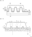
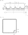
- FIG. 4 is a conceptual view of a semiconductor device according to an embodiment of the present invention.
- a recess 128 may be disposed in the bottom surface of the second conductive semiconductor layer 127 and also in a portion of the first conductive semiconductor layer 124 through the active layer 126.
- a first conductive layer 165 includes a connection electrode 167 disposed in the recess 128 and electrically connected to the first conductive semiconductor layer 124.
- a first electrode 142 may be disposed between the connection electrode 167 and the first conductive semiconductor layer 124.
- the first electrode 142 may be an ohmic electrode.
- the distance between the top surface of the recess 128 and the top surface of the semiconductor structure may range from about 1 ⁇ m to about 4 ⁇ m.
- the distance between the top surface of the semiconductor structure and the top surface of the recess 128 is less then 1 ⁇ m, it is possible for there to be a reduction in reliability of an emitting device.
- the distance is greater than about 4 ⁇ m, it is possible for there to be a reduction in light extraction efficiency due to defects of the crystal disposed inside the semiconductor structure or the like.
- a second conductive layer 150 may be disposed under and electrically connected to the 2-1 conductive semiconductor layer.
- the second conductive layer 150 may be disposed between a plurality of connection electrodes 167.
- the second conductive layer 150 may be partially exposed and electrically connected to a second electrode pad 166.
- a second electrode 246 may be disposed between and electrically connected to the second conductive layer 150 and the 2-1 conductive semiconductor layer 127a.
- the surface layer of the 2-1 conductive semiconductor layer 127a may have a relatively low aluminum composition and thus facilitate an ohmic connection.
- the 2-1 conductive semiconductor layer 127a has a thickness greater than about 1 nm and less than about 30 nm and thus may have low light absorption.
- the first conductive layer 165 and the second conductive layer 150 may be made of a transparent conductive oxide (TCO).
- the transparent conductive oxide may be selected from among an indium tin oxide (ITO), an indium zinc oxide (IZO), an aluminum zinc oxide (AZO), an aluminum gallium zinc oxide (AGZO), an indium zinc tin oxide (IZTO), an indium aluminum zinc oxide (IAZO), an indium gallium zinc oxide (IGZO), an indium gallium tin oxide (IGTO), an antimony tin oxide (ATO), a gallium zinc oxide (GZO), an IZO nitride (IZON), ZnO, IrO x , RuO x , and NiO.
- ITO indium tin oxide
- IZO indium zinc oxide
- AZO aluminum zinc oxide
- AGZO aluminum gallium zinc oxide
- IZTO indium zinc tin oxide
- IAZO indium aluminum zinc oxide
- IGZO indium gallium zinc oxide
- the first conductive layer 165 and the second conductive layer 150 may include an opaque metal such as Ag, Ni, Al, Rh, Pd, Ir, Ru, Mg, Zn, Pt, Au, and Hf.
- the first conductive layer 165 may be formed in single or multiple layers in which a TCO and an opaque metal are mixed, but is not limited thereto.
- An insulation layer 130 may be made of at least one material selected from a group consisting of SiO 2 , Si x O y , Si 3 N 4 , Si x N y , SiO x N y , Al 2 O 3 , TiO 2 , and AlN, but is not limited thereto.
- the insulation layer 130 may electrically insulate the connection electrode from the active layer 126 and the second conductive semiconductor layer 127.
- FIG. 5 is a conceptual view of a semiconductor device according to another embodiment of the present invention.
- FIG. 5 shows a semiconductor structure 120A according to the configuration of FIG. 1 .
- the first electrode 142 may be disposed on top of the recesses 128 and electrically connected with the first conductive semiconductor layer 124.
- a second electrode 246 may be formed under the second conductive semiconductor layer 127.
- the second electrode 246 may be brought into contact with and electrically connected to the 2-1 conductive semiconductor layer 127a.
- the 2-1 conductive semiconductor layer 127a in contact with the second electrode 246 may have an aluminum composition of 1% to 20%, it may thus facilitate an ohmic connection with the second electrode 246. Also, the 2-1 conductive semiconductor layer 127a has a thickness greater than about 1 nm and less than about 30 nm and thus may have low light absorption.
- Both the first electrode 142 and the second electrode 246 may be an ohmic electrode. Both the first electrode 142 and the second electrode 246 may be made of at least one of indium tin oxide (ITO), indium zinc oxide (IZO), indium zinc tin oxide (IZTO), indium aluminum zinc oxide (IAZO), indium gallium zinc oxide (IGZO), indium gallium tin oxide (IGTO), aluminum zinc oxide (AZO), antimony tin oxide (ATO), gallium zinc oxide (GZO), IZO nitride (IZON), Al-Ga ZnO (AGZO), In-Ga ZnO (IGZO), ZnO, IrOx, RuOx, NiO, RuOx/ITO, Ni/IrOx/Au, Ni/IrOx/Au/ITO, Ag, Ni, Cr, Ti, Al, Rh, Pd, Ir, Sn, In, Ru, Mg, Zn, Pt, Au, and Hf, but is not
- a second electrode pad 166 may be disposed in an edge of the semiconductor device. Since the second electrode pad 166 is disposed in a region from which a first insulation layer 131 and a passivation layer 180 are partially removed, the second electrode pad 166 may have a recessed central portion and also have a top surface having a concave portion and a convex portion. A wire (not shown) may be bonded to the concave portion of the top surface. Accordingly, since the bonding area increases, the second electrode pad 166 may be strongly bonded to the wire.
- the second electrode pad 166 may serve to reflect light. Thus, as the second electrode pad 166 gets closer to the semiconductor structure 120, it is possible to enhance light extraction efficiency.
- the convex portion of the second electrode pad 166 may be higher than the active layer 126. Accordingly, the second electrode pad 166 may enhance light extraction efficiency and control the beam angle by upwardly reflecting light emitted from the active layer 126 in a direction horizontal to the device.
- the first insulation layer 131 is partially opened under the second electrode pad 166 so that the second conductive layer 150 and the second electrode may be electrically connected to each other.
- the passivation layer 180 may be formed on top of and on the side of the semiconductor structure 120. The passivation layer 180 may be in contact with a region adjacent to the second electrode 246 or to the first insulation layer under the second electrode 246.
- the opened part of the first insulation layer 131 where the second electrode pad 166 is in contact with the second conductive layer 150 may have a width d22 ranging, for example, from about 40 ⁇ m to about 90 ⁇ m.
- the opening part has a width less than about 40 ⁇ m, the operating voltage may increase.
- the opened part has a width greater than about 90 ⁇ m, it may be difficult to secure a processing margin for preventing exposure of the second conductive layer 150 to the outside.
- the width d22 may preferably range from 60% to 95% of the entire width of the second electrode pad 166.
- the first insulation layer 131 may electrically insulate the first electrode 142 from the active layer 126 and the second conductive semiconductor layer 127. Also, the first insulation layer 131 may electrically insulate the second electrode 246 and the second conductive layer 150 from the first conductive layer 165.
- the first insulation layer 131 may be made of at least one material selected from the group consisting of SiO 2 , Si x O y , Si 3 N 4 , Si x N y , SiO x N y , Al 2 O 3 , TiO 2 , and AlN, but is not limited thereto.
- the first insulation layer 131 may be formed in single or multiple layers.
- the first insulation layer 131 may be a distributed Bragg reflector (DBR) having a multi-layered structure including an Si oxide or a Ti compound.
- DBR distributed Bragg reflector
- the present invention is not limited thereto, and the first insulation layer 131 may include various reflective structures.
- the first insulation layer 131 When the first insulation layer 131 has a reflective function, the first insulation layer 131 may upwardly reflect light emitted horizontally from the active layer 126, thereby enhancing light extraction efficiency. As described below, the light extraction efficiency may increase as the recesses 128 in an ultraviolet semiconductor device increase in number
- the second conductive layer 150 may be disposed under the second electrode 246. Accordingly, the second electrode pad 166, the second conductive layer 150, and the second electrode 246 may form one electrical channel.
- the second conductive layer 150 may entirely surround the second electrode 246 and may be in contact with the side surface and the top surface of the first insulation layer 131.
- the second conductive layer 150 may be made of a material having good adhesion to the first insulation layer 131 and may also be made of at least one material selected from a group consisting of Cr, Al, Ti, Ni, and Au or an alloy thereof.
- the second conductive layer 150 may be made in single or multiple layers.
- the second conductive layer 150 When the second conductive layer 150 is in contact with the side surface and the top surface of the first insulation layer 131, it is possible to enhance the thermal and electrical reliability of the second electrode 246. Also, the second conductive layer 150 may have a reflective function for upwardly reflecting light emitted from a gap between the first insulation layer 131 and the second electrode 246.
- the second conductive layer 150 may also be disposed a second separation distance, that is, disposed in a region where the second conductive semiconductor layer is exposed between the first insulation layer 131 and the second electrode 246.
- the second conductive layer 150 may be disposed in contact with a side surface and the top surface of the second electrode 246 and the side surface and the top surface of the first insulation layer 131 at the second separation distance.
- a region where a Schottky junction is formed by the second conductive semiconductor layer 127 coming into contact with the second conductive layer 150 may be disposed within the second separation distance.
- the second insulation layer 132 may electrically insulate the second electrode 246 and the second conductive layer 150 from the first conductive layer 165.
- the first conductive layer 165 may be electrically connected to the first electrode 142 via the second insulation layer 132.
- the first conductive layer 165 and a junction layer 160 may be disposed according to the bottom surface of the semiconductor structure 120 and the shape of the recesses 128.
- the first conductive layer 165 may be made of a material having good reflectivity.
- the first conductive layer 165 may include aluminum.
- the first conductive layer 165 may serve to upwardly reflect light emitted by the active layer 126, thereby enhancing light extraction efficiency.
- the junction layer 160 may include a conductive material.
- the junction layer 160 may include a material selected from a group consisting of gold, tin, indium, aluminum, silicon, silver, nickel, and copper or an alloy thereof.
- a substrate 170 may be made of a conductive material.
- the substrate 170 may include a metal or a semiconductor material.
- the substrate 170 may be made of a metal having good electrical conductivity and/or thermal conductivity. In this case, heat generated while the semiconductor device operates may be quickly released to the outside.
- the substrate 170 may include a material selected from a group consisting of silicon, molybdenum, tungsten, copper, and aluminum or an alloy thereof.
- a square wave pattern may be formed on top of the semiconductor structure 120.
- the square wave pattern may enhance the extraction efficiency of light emitted from the semiconductor structure 120.
- the square wave pattern may have a different average height depending on ultraviolet wavelengths. For UV-C, the average height ranges from about 300 nm to about 800 nm. When the height ranges from about 500 nm to about 600 nm, it is possible to enhance light extraction efficiency.
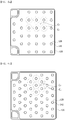
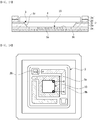
- FIGS. 6A and 6B are plan views of a semiconductor device according to an embodiment of the present invention.
- the active layer 126 may have an increasing quantity of light emitted to the side relative to a GaN-based blue light emitting device (TM mode).
- the TM mode may be performed by an ultraviolet semiconductor device.
- a larger number of recesses 128 may be formed on a GaN semiconductor that emits light having an ultraviolet wavelength band than on a GaN semiconductor that emits blue light, and then the first electrode 142 may be disposed in each of the recesses 128.
- an electric current may be distributed only to points adjacent to the first electrode 142, and electric current density may rapidly decrease at points apart from the first electrode 142. Accordingly, it is possible for an effective light emitting region C2 to become narrow.
- a region up to a boundary having an electric current density of 40% or less with respect to a point adjacent to the first electrode 142 and having the highest electric current density may be defined as the effective light emitting region C2.
- the effective light emitting region C2 may be adjusted in the range of about 5 ⁇ m to about 40 ⁇ m from the center of each of the recesses 128 depending on the injected electric current level and aluminum composition.
- a low electric current density region C3 which is a region between adjacent first electrodes 142, has a low electric current density and thus hardly contributes to light emission. Accordingly, according to an embodiment of the present invention, a first electrode 142 may be additionally disposed in the low electric current density region C3, which has a low electric current density, thereby enhancing optical output power.
- the areas of the recesses 128 and the first electrodes 142 be minimized. This is because the area of the active layer 126 decreases as the areas of the recess 128 and the first electrode 142 increase.
- the GaN semiconductor layer has lower electric current distribution characteristics than a semiconductor device that emits blue light because of a high aluminum composition. Accordingly, it may be preferable to reduce size of the low electric current density region C3 by increasing the number of first electrodes 142 while reducing the area of the active layer 126.
- the recesses 128 when the number of recesses 128 is 48, the recesses 128 cannot be straightly arranged in a horizontal or vertical direction and may be arranged in a zigzag form. In this case, since the area of the low electric current density region C3 is further decreased, most of the active layer may participate in light emission.
- the number of recesses 128 ranges from about 70 to about 110, an electric current may be efficiently distributed. Thus, it is possible to additionally decrease operating voltage and enhance optical output power.
- the number of recesses 128 when the number of recesses 128 is less than about 70, it is possible to reduce electrical characteristics and optical characteristics.
- the number of recesses 128 is greater than about 110, it is possible to enhance electrical characteristics, but there may be a reduction in optical characteristics due to the reduction in volume of the light emitting layer.
- a first area in which a plurality of first electrodes 142 are in contact with the first conductive semiconductor layer 124 may range from about 7.4% to about 20% or from about 10% to about 20% of the maximum horizontal sectional area of the semiconductor structure 120.
- the first area may be the sum of areas in which the first electrodes 142 are in contact with the first conductive semiconductor layer 124.
- the first area of the plurality of first electrodes 142 is greater than or equal to 7.4% of the maximum horizontal sectional area of the semiconductor structure 120, it is possible to have sufficient electric current distribution characteristics and enhance optical output power.
- the first area is less than or equal to 20% of the maximum horizontal sectional area of the semiconductor structure 120, it is possible to improve optical output power and operating voltage characteristics by securing areas of the active layer and the second electrodes.
- the total area of the plurality of recesses 128 may range from 13% to 30% of the maximum horizontal sectional area of the semiconductor structure 120. When the total area of the recesses 128 does not fall within this range, it may be difficult to keep the total area of the first electrode 142 within the range of about 7.4% to about 20%. Also, this may cause an increase in operating voltage and a decrease in optical output power.
- a second area in which the second electrode 246 is in contact with the second conductive semiconductor layer 127 may range from about 35% to about 70% of the maximum horizontal sectional area of the semiconductor structure 120.
- the second area may be the total area in which the second electrode 246 is in contact with the second conductive semiconductor layer 127.
- the second area is greater than or equal to 35%, it is possible to ensure the area of the second electrode and thus to enhance injection efficiency for second carriers and enhance operating voltage characteristics. Also, when the second area is less than or equal to 70%, it is possible to effectively widen the first area and thus improve injection efficiency for first carriers.
- the first area is inversely proportional to the second area. That is, when the number of recesses is increased to increase the number of first electrodes, the area of the second electrode decreases. In order to increase optical output power, the first carriers should be balanced with the second carriers. Thus, it is important to determine an appropriate ratio between the first area and the second area.
- a ratio of the first area in which the plurality of first electrodes are in contact with the first conductive semiconductor layer to the second area in which the second electrode is in contact with the second conductive semiconductor layer may range from 1: 3 to 1: 10.
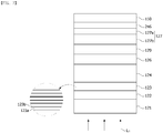
- FIG. 7 is a conceptual diagram of a semiconductor structure grown on a substrate
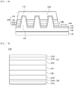
- FIG. 8 is a diagram illustrating a substrate separation process
- FIG. 9 is a diagram illustrating a semiconductor structure etching process
- FIG. 10 is a diagram showing a manufactured semiconductor device.
- a buffer layer 122, a light absorption layer 123, a first conductive semiconductor layer 124, an active layer 126, a second conductive semiconductor layer 127, a second electrode 246, and a second conductive layer 150 may be sequentially formed on a growth substrate 121.
- the light absorption layer 123 includes a first light absorption layer 123a having a low aluminum composition and a second light absorption layer 123b having a high aluminum composition.
- a plurality of first light absorption layers 123a and a plurality of second light absorption layers 123b may be alternately disposed.
- the first light absorption layer 123a may have a lower aluminum composition than the first conductive semiconductor layer 124.
- the first light absorption layer 123a may be separated when absorbing laser light during a laser lift-off (LLO) process. Accordingly, it is possible to remove the growth substrate.
- LLO laser lift-off
- the thickness and aluminum composition of the first light absorption layer 123a may be appropriately adjusted to absorb laser light having a predetermined wavelength (e.g., 246 nm).
- the first light absorption layer 123a may have an aluminum composition ranging from about 20% to about 50% and a thickness ranging from about 1 nm to about 10 nm.
- the first light absorption layer 123a may be made of AlGaN, but is not limited thereto.
- the second light absorption layer 123b may have a higher aluminum composition than the first conductive semiconductor layer 124. Accordingly, it is possible to enhance crystallinity of the first conductive semiconductor layer 124, which is grown on the light absorption layer 123, because a total aluminum composition decreased by the first light absorption layer 123a is increased by the second light absorption layer 123b.
- the second light absorption layer 123b may have an aluminum composition ranging from about 60% to about 100% and a thickness ranging from about 0.1 nm to about 2.0 nm.
- the second light absorption layer 123b may be made of AlGaN or AlN.
- the first light absorption layer 123a may be thicker than the second light absorption layer 123b.
- the thickness of the first light absorption layer 123a may range from about 1 nm to about 10 nm, and the thickness of the second light absorption layer 123b may range from about 0.5 nm to about 2.0 nm.
- the thickness ratio of the first light absorption layer 123a to the second light absorption layer 123b may range from 2:1 to 6:1. When the thickness ratio is less than 2:1, the first light absorption layer 123a is so thin that laser light cannot be sufficiently absorbed. When the thickness ratio is greater than 6:1, the second light absorption layer 123b is so thin that the total aluminum composition of the light absorption layer may be reduced.
- the light absorption layer may have a total thickness greater than about 100 nm and less than about 400 nm.
- the thickness is less than about 100 nm, the first light absorption layer 123a is so thin that it is difficult to absorb 246 nm laser light.
- the thickness is greater than about 400 nm, the total aluminum composition is reduced and thus crystallinity deteriorates.
- the light absorption layer 123 may function as a buffer layer for alleviating a lattice mismatch between the growth substrate 121 and the semiconductor structure 120.
- a step of removing the growth substrate 121 may include separating the growth substrate 121 by emitting laser L1 from the side where the growth substrate 121 is present.
- the laser L1 may have a wavelength band absorbable by the first light absorption layer 123a.
- the laser may be a KrF laser having a wavelength band of 248 nm.
- the growth substrate 121 and the second light absorption layer 123b have high energy band gaps and thus do not absorb laser L1.
- the first light absorption layer 123a having a low aluminum composition may be disassembled by absorbing laser L1. Accordingly, it is possible to separate the first light absorption layer 123a together with the growth substrate 121.
- a residual light absorption layer 123-2 on the first conductive semiconductor layer 124 may be removed through a labeling process.
- a plurality of recesses 128 may be formed to pass through up to a portion of the first conductive semiconductor layer 124 of the semiconductor structure 120. Subsequently, an insulation layer 130 may be formed at the side of each of the recesses 128 and over the second conductive semiconductor layer 127. Subsequently, a first electrodes 142 may be formed on the first conductive semiconductor layer 124 exposed by each of the recesses 128.
- a first conductive layer 165 may be formed under the insulation layer 130.
- the first conductive layer 165 may be electrically insulated from the second conductive layer 150 by the insulation layer 130.
- a conductive substrate 170 may be formed under the first conductive layer 165, and a second electrode pad 166 may be formed on a portion of the second conductive layer 150 that is exposed through a mesa etching process.
- FIG. 11 is a conceptual diagram of a semiconductor structure according to the third embodiment of the present invention
- FIG. 12 is a graph showing an aluminum composition of the semiconductor structure according to the third embodiment of the present invention
- a semiconductor device includes a semiconductor structure 120 including a first conductive semiconductor layer 124, a second conductive semiconductor layer 127, and an active layer 126 disposed between the first conductive semiconductor layer 124 and the second conductive semiconductor layer 127.
- the first conductive semiconductor layer 124 may include a 1-1 conductive semiconductor layer 124a, a 1-2 conductive semiconductor layer 124c, and an intermediate layer 124b disposed between the 1-1 conductive semiconductor layer 124a and the 1-2 conductive semiconductor layer 124c.
- the 1-2 conductive semiconductor layer 124c may be disposed closer to the active layer 126 than the 1-1 conductive semiconductor layer 124a.
- the 1-2 conductive semiconductor layer 124c may have a lower aluminum composition than the 1-1 conductive semiconductor layer 124a.
- the aluminum composition of the 1-2 conductive semiconductor layer 124c may range from about 40% to about 70%, and the aluminum composition of the 1-1 conductive semiconductor layer 124a may range from about 50% to about 80%.
- the 1-2 conductive semiconductor layer 124c may be thinner than the 1-1 conductive semiconductor layer 124a.
- the 1-1 conductive semiconductor layer 124a may have a thickness ranging from about 130% to about 500% of the thickness of the 1-2 conductive semiconductor layer 124c.
- the intermediate layer 124b disposed on the 1-1 conductive semiconductor layer 124a, the 1-2 conductive semiconductor layer 124c, or the like may have reduced crystallinity.
- the semiconductor structure When the thickness of the 1-1 conductive semiconductor layer 124a is greater than about 150%, the semiconductor structure is thick enough to cause stress to be applied to the semiconductor structure that is high enough to crack the semiconductor structure or change the wavelength of emitted light. According to such a configuration, the intermediate layer 124b is formed after the 1-1 conductive semiconductor layer 124a, which has a high aluminum composition, is sufficiently grown. Accordingly, it is possible to enhance the overall crystallinity of the semiconductor structure 120 and also adjust the wavelength of emitted light according to the user's desire.
- the intermediate layer 124b may have a smaller aluminum composition than the first conductive semiconductor layer 124.
- the intermediate layer 124b may serve to absorb laser light emitted to the semiconductor structure during an LLO process to prevent damage to the active layer 126. Accordingly, the semiconductor device according to an embodiment of the present invention can reduce damage to the active layer, thereby enhancing optical power and electrical characteristics.
- the thickness and aluminum composition of the intermediate layer 124b may be appropriately adjusted to absorb laser light emitted to the semiconductor structure 120 during an LLO process.
- the intermediate layer 124b may have an aluminum composition ranging from about 30% to about 60% and a thickness ranging from about 1 nm to about 10 nm.
- the intermediate layer 124b may be made of AlGaN, but is not limited thereto.
- the intermediate layer 124b may be disposed between the first conductive semiconductor layer 124 and the active layer 126. Also, the intermediate layer 124b may include a first intermediate layer having a lower aluminum composition than the first conductive semiconductor layer 124 and a second intermediate layer having a higher aluminum composition than the first conductive semiconductor layer 124. A plurality of first intermediate layers and a plurality of second intermediate layers may be alternately disposed.
- the active layer 126 may be disposed between the first conductive semiconductor layer 124 and the second conductive semiconductor layer 127.
- the active layer 126 is a layer in which electrons (or holes) injected through the first conductive semiconductor layer 124 are combined with holes (or electrons) injected through the second conductive semiconductor layer 127.
- the second conductive semiconductor layer 127 may be formed on the active layer 126 may be made of a group III-V or group II-VI compound semiconductor and may also be doped with a second dopant.
- the second conductive semiconductor layer 127 may be made of a semiconductor material having an empirical formula In x5 Al y2 Ga 1-x5-y2 N (0 ⁇ x5 ⁇ 1, 0 ⁇ y2 ⁇ 1, and 0 ⁇ x5+y2 ⁇ 1) or a material selected from among AlInN, AlGaAs, GaP, GaAs, GaAsP, and AlGaInP.
- the second dopant is a p-type dopant such as Mg, Zn, Ca, Sr, and Ba
- the second conductive semiconductor layer 127 doped with the second dopant may be a p-type semiconductor layer.
- the second conductive semiconductor layer 127 may include a 2-1 conductive semiconductor layer 127a, a 2-2 conductive semiconductor layer 127b, and a 2-3 conductive semiconductor layer 127c.
- the 2-1 conductive semiconductor layer 127a may have a lower aluminum composition than the 2-2 conductive semiconductor layer 127b.
- a blocking layer 129 may be disposed between the active layer 126 and the second conductive semiconductor layer 127.
- the blocking layer 129 may block first carriers (e.g., electrons) supplied from the first conductive semiconductor layer 124 from flowing out to the second conductive semiconductor layer 127.
- the first conductive semiconductor layer 124, the active layer 126, the second conductive semiconductor layer 127, and the blocking layer 129 may all include aluminum. Accordingly, the first conductive semiconductor layer 124, the active layer 126, the second conductive semiconductor layer 127, and the blocking layer 129 may have an AlGaN composition.
- the blocking layer 129 may have an aluminum composition ranging from about 50% to about 100%. When the aluminum composition of the blocking layer 129 is less than about 50%, an energy barrier for blocking electrons may be insufficient in height, and the blocking layer 129 may absorb light emitted from the active layer 126.
- the blocking layer 129 may include a 1-1 section 129a and a 1-2 section 129c.
- the blocking layer 129 may include a second dopant.
- the second dopant may include a p-type dopant such as Mg, Zn, Ca, Sr, and Ba.
- the blocking layer 129 may include a dopant that is identical to that of the second conductive semiconductor layer.
- the present invention is not limited thereto, and the blocking layer 129 may have the same polarity as the second conductive semiconductor layer 127 and may include a second dopant that is different from that of the second conductive semiconductor layer.
- the 1-1 section 129a may have an aluminum composition increasing toward the second conductive semiconductor layer 127.
- the region of highest aluminum composition in the 1-1 section 129a may have an aluminum composition ranging from about 80% to about 100%. That is, the 1-1 section 129a may be made of AlGaN or AIN. Alternatively, the 1-1 section 129a may be a superlattice layer in which AlGaN and AIN are alternately disposed.
- the 1-1 section 129a may have a thickness ranging from about 0.1 nm to about 4 nm.
- first carriers e.g., electrons
- second carriers e.g., holes
- the 1-2 section 129c may serve to efficiently block movement of the first carriers (e.g., electrons).
- the 1-2 section 129c may include a second dopant in order to enhance injection of second carriers (e.g., holes).
- the second dopant may include a p-type dopant such as Mg, Zn, Ca, Sr, and Ba.
- the 1-2 section 129c may have a thickness ranging from about 15 nm to about 30 nm. When the thickness is less than about 15 nm, it may not be possible to efficiently block movement of first carriers (e.g., electrons). Also, when the thickness is greater than about 30 nm, it is possible for there to be a reduction in the efficiency with which second carriers (e.g., holes) are injected into the active layer.
- An undoped section 129b which is not doped with Mg, may be disposed between the 1-1 section 129a and the 1-2 section 129c.
- the undoped section 129b may serve to prevent a dopant included in the second conductive semiconductor layer 127 from diffusing from the second conductive semiconductor layer 127 to the active layer 126.
- the undoped section 129b may have a thickness ranging from about 10 nm to about 15 nm. When the thickness is less than about 10 nm, it may be difficult to prevent a dopant from diffusing to the active layer 126. When the thickness is greater than about 15 nm, it is possible for there to be a reduction in the efficiency with which second carriers (e.g., holes) are injected.
- the second conductive semiconductor layer 127 may include a 2-1 conductive semiconductor layer 127a, a 2-2 conductive semiconductor layer 127b, and a 2-3 conductive semiconductor layer 127c.
- the 2-2 conductive semiconductor layer 127b may have a thickness greater than about 10 nm and less than about 50 nm.
- the 2-2 semiconductor layer 127b may have a thickness equal to about 25 nm.
- the 2-2 conductive semiconductor layer 127b has a thickness less than about 10 nm, it is possible to reduce electric current injection efficiency because of a horizontal increase in resistance.
- the 2-2 conductive semiconductor layer 127b has a thickness greater than about 50 nm, it is possible for there to be a reduction in electric current injection efficiency because of an increase in resistance in the horizontal direction.
- the 2-2 conductive semiconductor layer 127b may have a higher aluminum composition than the well layer 126a.
- the well layer 126a may have an aluminum composition ranging from about 30% to about 70%.
- the 2-2 conductive semiconductor layer 127b has a lower aluminum composition than the well layer 126a, it is possible for there to be a reduction in light extraction efficiency because the 2-2 conductive semiconductor layer 127b absorbs light.
- the present invention is not limited thereto.
- the 2-2 conductive semiconductor layer 127b may have a lower aluminum composition than the well layer 126a.
- the 2-2 conductive semiconductor layer 127b may have an aluminum composition greater than about 40% and less than about 80%.
- the aluminum composition of the 2-2 conductive semiconductor layer 127b is less than about 40%, light may be absorbed.
- the aluminum composition of the 2-2 conductive semiconductor layer 127b is greater than about 80%, electric current injection efficiency may deteriorate.
- the well layer 126a has an aluminum composition of about 30%
- the 2-2 conductive semiconductor layer 127b may have an aluminum composition of about 40%.
- the 2-1 conductive semiconductor layer 127a may have a lower aluminum composition than the well layer 126a.
- the 2-1 conductive semiconductor layer 127a has a higher aluminum composition than the well layer 126a, the 2-1 conductive semiconductor layer 127a is not sufficiently ohmic with a second electrode due to an increase in resistance therebetween, and electric current injection efficiency is also reduced.
- the 2-1 conductive semiconductor layer 127a may have an aluminum composition greater than about 1% and less than about 50%. When the aluminum composition is greater than about 50%, the 2-1 conductive semiconductor layer 127a may not be sufficiently ohmic with the second electrode. When the aluminum composition is less than about 1%, the composition is close to GaN, and thus the 2-1 conductive semiconductor layer 127a absorbs light.
- the 2-1 conductive semiconductor layer 127a may have a thickness ranging from about 1 nm to about 30 nm or ranging from about 1 nm to about 10 nm. As described above, the 2-1 conductive semiconductor layer 127a may absorb ultraviolet light because the 2-1 conductive semiconductor layer 127a has an aluminum composition low enough to be ohmic. Accordingly, it may be advantageous in terms of optical output power to control the 2-1 conductive semiconductor layer 127a to be as thin as possible.
- the thickness of the 2-1 conductive semiconductor layer 127a is controlled to be less than or equal to about 1 nm, it is possible for there to be a reduction in crystallinity due to a change in aluminum composition. Also, the 2-1 conductive semiconductor layer 127a is so thin that horizontal resistance of the 2-1 conductive semiconductor layer 127a may increase and the electrical characteristics of the semiconductor device may decrease. Also, when the thickness is greater than about 30 nm, the absorbed light quantity is large enough that optical output power efficiency may decrease.
- the 2-1 conductive semiconductor layer 127a may have a smaller thickness than the 2-2 conductive semiconductor layer 127b.
- the thickness ratio of the 2-2 conductive semiconductor layer 127b to the 2-1 conductive semiconductor layer 127a may range from 1.5:1 to 20:1. When the thickness ratio is less than 1.5:1, the 2-2 conductive semiconductor layer 127 is thin enough that the electric current injection efficiency may decrease. When the thickness ratio is greater than 20:1, the 2-1 conductive semiconductor layer 127a is thin enough that crystallinity may be reduced and the electrical characteristics of the semiconductor device may be reduced.
- the 2-2 conductive semiconductor layer 127b may have an aluminum composition decreasing away from the active layer 126.
- the 2-1 conductive semiconductor layer 127a may have an aluminum composition decreasing away from the active layer 126.
- the 2-1 conductive semiconductor layer 127a may have a greater reduction in aluminum composition than the 2-2 conductive semiconductor layer 127b. That is, the 2-1 conductive semiconductor layer 127a may have a greater variation in aluminum composition in the direction of thickness than the 2-2 conductive semiconductor layer 127b.
- the 2-2 conductive semiconductor layer 127b is thicker than the 2-1 conductive semiconductor layer 127a and has a higher aluminum composition than the well layer 126a, and thus may have a relatively low reduction in aluminum composition.
- the 2-1 conductive semiconductor layer 127a is thin and has a large change in aluminum composition, a reduction in aluminum composition may be relatively large. Since the 2-1 conductive semiconductor layer 127a is thin and has a large change in aluminum composition, it is possible to change the aluminum composition while relatively slowly growing the 2-1 conductive semiconductor layer 127a.
- the 2-3 conductive semiconductor layer 127c may have a uniform aluminum composition.
- the 2-3 conductive semiconductor layer 127c may have a thickness ranging from about 20 nm to about 60 nm.
- the 2-3 conductive semiconductor layer 127c may have an aluminum composition ranging from about 40% to about 70%.
- the aluminum composition of the 2-3 conductive semiconductor layer 127c is greater than or equal to about 40%, it is possible for there to be a reduction in crystallinity of the 2-1 conductive semiconductor layer 127a and the 2-2 conductive semiconductor layer 127b.
- the aluminum composition is less than about 70%, it is possible to prevent reduction of the crystallinity due to a rapid change in aluminum composition of the 2-1 conductive semiconductor layer 127a and the 2-2 conductive semiconductor layer 127b.
- the 2-1 conductive semiconductor layer 127a may have a thickness ranging from about 1 nm to about 10 nm
- the 2-2 conductive semiconductor layer 127b may have a thickness ranging from about 10 nm to about 50 nm
- the 2-3 conductive semiconductor layer 127c may have a thickness ranging from about 20 nm to about 60 nm.
- the ratio of the thickness of the 2-1 conductive semiconductor layer 127a to the total thickness of the second conductive semiconductor layer 127 may range from 1:3 to 1:120. When the ratio is greater than 1:3, the 2-1 conductive semiconductor layer 127a may ensure the electrical characteristics (e.g., an operating voltage) of the semiconductor device.
- the 2-1 conductive semiconductor layer 127a may ensure the optical characteristics (e.g., optical output power) of the semiconductor device.
- the present invention is not limited thereto, and the ratio of the thickness of the 2-1 conductive semiconductor layer 127a to the total thickness of the second conductive semiconductor layer 127 may range from 1:3 to 1:150 or range from 1:3 to 1:70.
- FIG. 13 is a secondary ion mass spectrometry (SIMS) graph showing the change in aluminum strength of the semiconductor structure according to the third embodiment of the present invention
- FIG. 14 is a partially enlarged view of FIG. 13 .
- the semiconductor structure may have aluminum ion strength that changes from the first conductive semiconductor layer 124 to the second conductive semiconductor layer 127.
- SIMS data may be analyzed through Time-of-Flight secondary ion mass spectrometry (TOF-SIMS).
- TOF-SIMS Time-of-Flight secondary ion mass spectrometry
- SIMS data may be analyzed by emitting primary ions to a target surface and counting the number of secondary ions discharged.
- the primary ions may be selected from among O 2 + , Cs + , Bi + , and so on, an acceleration voltage may be adjusted between the range of about 20 keV to about 30 KeV, an emitted current may be adjusted between the range of about 0.1 pA to about 5.0 pA, and a target area may be 20 nm ⁇ 20 nm.
- SIMS data may be obtained by collecting a secondary ion mass spectrum while gradually etching a surface of the second conductive semiconductor layer in a direction toward the first conductive semiconductor layer.
- the secondary ions may each be an aluminum ion.
- a spectrum of aluminum ion strength may be expressed on a linear scale, but the present invention is not limited thereto.
- the spectrum may also be expressed on a log scale.
- the semiconductor structure may have a first point P1 with the lowest aluminum ion strength in the first conductive semiconductor layer 124, a second point P2 with the highest aluminum ion strength in the blocking layer, and a third point P3 with the lowest aluminum ion strength in the second conductive semiconductor layer 127.
- the present invention is not limited thereto, and the point of highest aluminum ion strength and the point of lowest aluminum ion strength in the semiconductor structure may be different from those described above.
- the first point P1 may be positioned in the intermediate layer 124b that is disposed in the first conductive semiconductor layer, and may be a region that is in contact with the first electrode 142.
- the second point P2 may be positioned in the 1-1 section 129a of the blocking layer 129.
- the third point P3 may be positioned in a contact layer (the 2-1 conductive semiconductor layer) where the second conductive semiconductor layer is in direct contact with the second electrode (a P-ohmic electrode).
- a semiconductor layer of a certain thickness or greater may include noise.
- the first point P1 may be defined as a layer having the same strength as a layer having low aluminum ion strength in the first conductive semiconductor layer.
- noise at the first point P1 may be 2% or less of the difference between the high point and the low point
- the ratio of the difference in aluminum strength between the first point P1 and the second point P2, called D1, to the difference in aluminum strength between the first point P1 and the third point P3, called D2, (i.e., D1:D2) may range from 1:0.2 to 1:2.
- the ratio is less than or equal to 1:2, by preventing a relative increase in the second aluminum strength difference D2, it is possible to adjust the change in aluminum strength with respect to the thickness of the 2-1 conductive semiconductor layer 127a such that the change does not become too large Accordingly, it is possible to improve crystallinity of the semiconductor structure and improve transmittance of the 2-1 conductive semiconductor layer 127a with respect to light emitted by the active layer 126 to enhance the optical characteristics of the semiconductor device.
- the GaN layer that is in contact with the electrode does not include aluminum.
- the ratio of the first aluminum strength difference D1 to the second aluminum strength difference D2 may depart from the range of 1:0.2 to 1:2.
- the ratio between the first thickness W1 of the semiconductor structure to the second thickness W2 of the semiconductor may range from 1:0.2 to 1:1.
- the first thickness W1 may be the thickness of the semiconductor structure between a fourth point P1 and a second point P2 positioned in the second conductive semiconductor layer 127
- the second thickness W2 may be the thickness of the semiconductor structure between the fourth point P1 and a third point P3 positioned in the second conductive semiconductor layer 127.
- the thickness ratio is less than or equal to 1:1, it is possible to relatively reduce the second thickness W2. Accordingly, it is possible to improve light extraction efficiency by alleviating the problem of light emitted by the active layer 126 being absorbed inside the second thickness W2.
- a first conductive semiconductor layer 124, an active layer 126, a blocking layer 129, and a second conductive semiconductor layer 127 may be sequentially stacked on the semiconductor structure.
- a second electrode may be brought in direct contact with the surface 127a of the second conductive semiconductor layer 127 to form an ohmic contact.
- FIG. 16 is a conceptual diagram of the second conductive semiconductor layer of FIG. 1
- FIG. 17 shows AFM data obtained by measuring the surface of the second conductive semiconductor layer according to the third embodiment of the present invention
- FIG. 18 shows AFM data obtained by measuring the surface of a GaN thin film
- FIG. 19 shows AFM data obtained by measuring the surface of a fast-grown second conductive semiconductor layer.
- a second conductive semiconductor layer 127 may include a 2-1 conductive semiconductor layer 127a, a 2-2 conductive semiconductor layer 127b, and a 2-3 conductive semiconductor layer 127c.
- the 2-1 conductive semiconductor layer 127a may be a contact layer that is in contact with the second electrode.
- the above-description may be applied as it is.
- the surface of the 2-1 conductive semiconductor layer 127a may include a plurality of clusters C1.
- Each of the clusters C1 may be a protrusion protruding from the surface.
- each of the clusters C1 may be a protrusion protruding more than about 10 nm or 20 nm from the average surface height.
- Each of the clusters C1 may be formed due to a lattice mismatch between aluminum Al and gallium Ga.
- the 2-1 conductive semiconductor layer 127a includes aluminum, has a large variation in thickness of aluminum, and is thinner than other layers.
- the surface may be formed not in a single layer but in the form of clusters C 1.
- Each of the clusters C1 may include Al, Ga, N, Mg, or the like. However, the present invention is not limited thereto.
- clusters C1 formed in the shape of relatively bright dots may be seen from the surface of the second conductive semiconductor layer 127.
- the surface since the 2-1 conductive semiconductor layer 127a has an aluminum composition ranging from about 1% to about 10%, the surface may be generated in the form of clusters C1 to increase contact area. Accordingly, it is possible to enhance electrical characteristics.
- 100 to 800 clusters C1 may be observed per average 100 ⁇ m 2 in the surface of the second conductive semiconductor layer 127.
- the average value is the average of values measured at about 10 or more different positions.
- the result obtained by measuring position E1 of FIG. 17 was 12 clusters C1 observed per unit area, which is 2 ⁇ m ⁇ 2 ⁇ m. Only clusters protruding more than 25 nm from the surface were measured as the clusters C1. By adjusting contrast in an AFM image, it is possible to ensure that only clusters protruding more than 25 nm from the surface may be output.
- the clusters C1 using converted units based on the measurement results, may have a density ranging from 1 ⁇ 10 -8 /cm 2 to 8 ⁇ 10 -6 /cm 2 .
- the density of the clusters C1 is greater than or equal to 1 ⁇ 10 -8 /cm 2 , the contact area may relatively increase, and contact resistance with the second electrode may decrease.
- the density of the clusters C1 is less than or equal to 8 ⁇ 10 -6 /cm 2 , it is possible to alleviate the problem of light emitted by the active layer 126 being absorbed by Ga included in some of the clusters. Accordingly, it is possible to improve optical output power.
- the density of the clusters C1 may satisfy 1 ⁇ 10 -8 /cm 2 to 8 ⁇ 10 -6 /cm 2 , and thus it is possible to decrease contact resistance with the second electrode while not reducing the optical output power.
- FIG. 19 it can be seen that clusters are not grown well when the second conductive semiconductor layer is fast-grown. Accordingly, it can be seen that no clusters C1 are formed when the second conductive semiconductor layer is fast-grown although the second conductive semiconductor layer is controlled such that the aluminum composition of the surface of the second conductive semiconductor layer ranges from about 1% to about 10%.
- FIG. 19 is a photograph obtained by measuring the surface after P-AlGaN is grown at a speed of 0.06nm/s.
- a contact layer should have an aluminum composition ranging from about 1% to about 10% and also a sufficiently low growth speed in order to form a plurality of clusters C1 in the second conductive semiconductor layer 127.
- the 2-1 conductive semiconductor layer may have a lower growth speed than the 2-2 conductive semiconductor layer and the 2-3 conductive semiconductor layer.
- the ratio of the growth speed of the 2-2 conductive semiconductor layer and the 2-1 conductive semiconductor layer may range from 1: 0.2 to 1: 0.8.
- the growth speed ratio is less than 1: 0.2, the growth speed of the 2-1 conductive semiconductor layer is so low that AlGaN having a high aluminum composition may be grown by Ga being etched at the same high temperature at which the AlGaN is grown, and thus reducing ohmic characteristics.
- the growth speed ratio is greater than 1: 0.8, the growth speed of the 2-1 conductive semiconductor layer is so high that the crystallinity may be reduced.
- FIG. 20 is a conceptual diagram of a semiconductor device according to the third embodiment of the present invention
- FIG. 21A is a plan view of FIG. 20
- FIG. 21B is a view enlarging a portion A of FIG. 20
- FIG. 22 is a plan view illustrating a portion of an interface between the second conductive semiconductor layer and the second electrode.
- a semiconductor structure 120 may have a configuration of the above-described semiconductor structure 120 applied as it is.
- a plurality of recesses 128 may be disposed even in a portion of a first conductive semiconductor layer 124 through a second conductive semiconductor layer 127 and an active layer 126.
- the semiconductor device may include a side reflector Z1 disposed on an edge thereof.
- the side reflector Z1 may be formed by a second conductive layer 150, a first conductive layer 165, and a substrate 170 protruding in the direction of thickness (a y-axis direction). Referring to FIG. 21A , the side reflector Z1 may be disposed along the edge of the semiconductor device to surround the semiconductor structure.
- the second conductive layer 150 of the side reflector Z1 protrudes further than the active layer 126 so that the second conductive layer 150 may upwardly reflect light L2 emitted by the active layer 126. Accordingly, without a separate reflective layer being formed, it is possible to reflect light emitted in a horizontal direction (an x-axis direction) upward at the outermost portion because of the TM mode.
- the side reflector Z1 may have a slope angle greater than about 90 degrees and less than about 145 degrees.
- the slope angle may be an angle between the second conductive layer 150 and the horizontal plane (an XZ plane). When the angle is less than about 90 degrees or greater than about 145 degrees, it is possible for there to be a reduction in the efficiency with which light traveling toward the side is reflected upward.
- a second electrode 246 may be in direct contact with a 2-1 conductive semiconductor layer 127a. As described above, clusters may be disposed on the surface of the 2-1 conductive semiconductor layer 127a to increase contact area with the second electrode 246.
- the second electrode 246 may be deposited on the 2-1 conductive semiconductor layer 127a.
- the second electrode is made of a metal oxide such as ITO
- the 2-1 conductive semiconductor layer 127a may come in contact with oxygen.
- an aluminum oxide may be formed by aluminum that is disposed on the surface of the 2-1 conductive semiconductor layer 127a to react with oxygen.
- a nitride such as NO and an oxide such as Ga 2 O 3 may be additionally formed.
- an aluminum oxide C2 may be observed at an interface between the second electrode 246 and the 2-1 conductive semiconductor layer 127a.
- the interface may be observed using a transmission electron microscope (TEM).
- FIG. 23 is a conceptual diagram of a semiconductor device package according to an embodiment of the present invention
- FIG. 24 is a plan view of the semiconductor device package according to an embodiment of the present invention
- FIG. 25 is a modification of FIG. 24 .
- the semiconductor device package may include a body 2 with a groove (an opening) 3, a semiconductor device 1 disposed in the body 2, and a pair of lead frames 5a and 5b disposed in the body 2 and electrically connected to the semiconductor device 1.
- the semiconductor device 1 may include all of the above-described elements.
- the body 2 may include a material or a coating layer that reflects ultraviolet light.
- the body 2 may be formed by stacking a plurality of layers 2a, 2b, 2c, 2d, and 2e.
- the plurality of layers 2a, 2b, 2c, 2d, and 2e may be made of the same material or include different materials.
- the plurality of layers 2a, 2b, 2c, 2d, and 2e may include an aluminum material.
- the groove 3 may have a width that increases away from the semiconductor device and may have an inclined surface having a stepped portion formed therein.
- a light transmitting layer 4 may cover the groove 3.
- the light transmitting layer 4 may be made of glass, but is not limited thereto. There is no limitation in material of the light transmitting layer 4 as long as the material can effectively transmit ultraviolet light.
- the groove 3 may have an empty space formed therein.
- a semiconductor device 10 may be disposed on a first lead frame 5a and connected with a second lead frame 5b by using a wire.
- the second lead frame 5b may be disposed to surround the first lead frame 5a.
- the semiconductor device package may have a plurality of semiconductor devices 10a, 10b, 10c, and 10d disposed therein.
- the lead frame may include a first lead frame 5a, a second lead frame 5b, a third lead frame 5c, a fourth lead frame 5d, and a fifth lead frame 5e.
- the first semiconductor device 10a may be disposed on the first lead frame 5a and connected with the second lead frame 5b using a wire.
- the second semiconductor device 10b may be disposed on the second lead frame 5b and connected with the third lead frame 5c by using a wire.
- the third semiconductor device 10c may be disposed on the third lead frame 5c and connected with the fourth lead frame 5d using a wire.
- the fourth semiconductor device 10d may be disposed on the fourth lead frame 5d and connected with the fifth lead frame 5e using a wire.
- the semiconductor device may be applied to various kinds of light source devices.
- the light source devices may include a sterilizing device, a curing device, a lighting device, a display device, and a vehicle lamp. That is, the semiconductor device may be applied in various electronic devices disposed in a housing and configured to provide light.
- the sterilizing device may have a semiconductor device to sterilize a desired region according to an embodiment of the present invention.
- the sterilizing device may be applied to home appliances such as a water purifiers, air conditioners, and refrigerators, but is not limited thereto. That is, the sterilizing device may be applied in various products needing to be sterilized (e.g., medical apparatuses).
- a water purifier may have the sterilizing device to sterilize circulating water according to an embodiment of the present invention.
- the sterilizing device may be placed at a nozzle or a discharging port through which water circulates and configured to emit ultraviolet light.
- the sterilizing device may include a waterproof structure.
- the curing device may have a semiconductor device to cure various kinds of liquids according to an embodiment of the present invention.
- the liquids may include various materials that are cured when ultraviolet light is emitted.
- the curing device may cure various types of resins.
- the curing device may also be applied to cure beauty products such as manicure products.
- the lighting device may, according to an embodiment of the present invention, include a light source module including a substrate and a semiconductor device, a heat dissipation unit configured to dissipate heat of the light source module, and a power supply unit configured to process or convert an electric signal from the outside and provide the electric signal to the light source module.
- the lighting device may include a lamp, a headlamp, or a streetlight.
- the display device may include a bottom cover, a reflective plate, a light emitting module, a light guide plate, an optical sheet, a display panel, an image signal output circuit, and a color filter.
- the bottom cover, the reflective plate, the light emitting module, the light guide plate, and the optical sheet may constitute a backlight unit.
- the reflective plate may be placed on the bottom cover, and the light emitting module may emit light.
- the light guide plate may be placed in front of the reflective plate to guide light emitted by the light emitting module forward.
- the optical sheet may include a prism sheet or the like and may be placed in front of the light guide plate.
- the display panel may be placed in front of the optical sheet.
- the image signal output circuit may supply an image signal to the display panel.
- the color filter may be placed in front of the display panel.
- the semiconductor device When the semiconductor device is used as a backlight unit of a display device, the semiconductor device may be used as an edge-type backlight unit or a direct-type backlight unit.
- the semiconductor device may be a laser diode rather than the above-described light emitting diode.
- the laser diode may include a first conductive semiconductor layer, an active layer, and a second conductive semiconductor layer that have the above-described structures.
- the laser diode may also utilize an electroluminescence phenomenon in which light is emitted when electric current flows after a p-type first conductive semiconductor and an n-type second conductive semiconductor are brought in contact with each other, but has a difference in the directionality and phase of the emitted light. That is, the laser diode uses stimulated emission and constructive interference so that light having a specific single wavelength may be emitted at the same phase and in the same direction. Due to these characteristics, the laser diode may be used for an optical communication device, a medical device, a semiconductor processing device, or the like.
- a light receiving device may include, for example, a photodetector, which is a kind of transducer configured to detect light and convert intensity of the light into an electric signal.
- the photodetector may include a photocell (silicon and selenium), an optical output element (cadmium sulfide and cadmium selenide), a photodiode (e.g., a PD with a peak wavelength in a visible blind spectral region or a true blind spectral region), a photo transistor, a photomultiplier, a photoelectric tube (vacuum and gas filling), an infra-red (IR) detector, or the like, but is not limited thereto.
- a photocell silicon and selenium
- an optical output element cadmium sulfide and cadmium selenide
- a photodiode e.g., a PD with a peak wavelength in a visible blind spectral region or a true blind spectral region
- a semiconductor device such as the photodetector may be produced using a direct bandgap semiconductor having good photoelectric transformation efficiency.
- the photodetector may have various structures.
- the photodetector may include a pin-type photodetector using a p-n junction, a Schottky photodetector using a Schottky junction, a metal-semiconductor-metal (MSM) photodetector, or the like.
- MSM metal-semiconductor-metal
- the photodiode may include a first conductive semiconductor layer and a second conductive semiconductor layer that have the above-described structures and may be formed as a p-n junction or a pin structure.
- the photodiode operates when a reverse bias or a zero bias is applied.
- When light is incident on the photodiode electrons and holes are generated such that electric current flows.
- the magnitude of electric current may be approximately proportional to intensity of light incident on the photodiode.
- a photocell or a solar cell which is a kind of photodiode, may convert light into electric current.
- the solar cell may include a first conductive semiconductor layer, an active layer, and a second conductive semiconductor layer that have the above-described structures.
- the solar cell may be used as a rectifier of an electronic circuit through the rectification characteristics of a general diode using a p-n junction and may be applied to an oscillation circuit or the like of a microwave circuit.
- the above-described semiconductor device is not necessarily implemented only with semiconductors.
- the semiconductor device may additionally include a metal material.
- a semiconductor device such as the light receiving device may be implemented using at least one of Ag, Al, Au, In, Ga, N, Zn, Se, P, and As and may be implemented using an intrinsic semiconductor material or a semiconductor material doped with a p-type dopant or an n-type dopant.
Landscapes
- Physics & Mathematics (AREA)
- Condensed Matter Physics & Semiconductors (AREA)
- General Physics & Mathematics (AREA)
- Electromagnetism (AREA)
- Optics & Photonics (AREA)
- Geometry (AREA)
- Led Devices (AREA)
- Led Device Packages (AREA)
Abstract
Description
- This application claims priority to and the benefit of Korean Patent Applications No.
2016-0112809, filed on September 01, 2016 2016-0163830, filed on December 02, 2016 - Embodiments relate to a semiconductor device and a semiconductor device package including the same.
- Semiconductor devices including compounds such as GaN and AlGaN have many merits such as wide and adjustable band gap energy and thus may be variously used as light emitting devices, light receiving devices, various kinds of diodes, or the like.
- In particular, light emitting devices using group III-V or II-VI compound semiconductors or light emitting devices such as a laser diode may implement various colors such as red, green, blue, and ultraviolet due to the development of thin film growth technology and device materials and implement efficient white light rays by using fluorescent materials or combining colors. These light emitting devices also have advantages with respect to low power consumption, semi-permanent life span, fast response time, safety, and environmental friendliness compared to conventional light sources such as a fluorescent lamp, an incandescent lamp, or the like.
- In addition, when light receiving devices such as optical detectors or solar cells are produced using group III-V or II-VI compound semiconductors, an optical current is generated by absorbing light in various wavelength ranges due to development of device materials, and thus light may be used in various wavelength ranges from gamma rays to radio wavelength regions. Also, the light receiving devices have the advantages of fast response time, stability, environmental friendliness, and ease of adjustment of device materials and may be easily used to power control or microwave circuits or communication modules.
- Accordingly, semiconductor devices are being extended and applied to the transmission modules of optical communication means, light emitting diode backlights substituted for cold cathode fluorescence lamps (CCFL) forming the backlights of liquid crystal display (LCD) devices, white light emitting diode lamps to be substituted for fluorescent bulbs, incandescent bulbs, car headlights, traffic lights, and sensors for detecting gas or fire. In addition, semiconductor devices may also be extended and applied to high-frequency application circuits or other power control devices and communication modules.
- In particular, a light emitting device that emits light in an ultraviolet wavelength range may be used for curing, medical, and sterilization purposes due to its curing or sterilizing action.
- Recently, research on ultraviolet light emitting devices has been actively conducted, but the ultraviolet light emitting devices are difficult to vertically realize and also have decreased crystallinity during the substrate separation process.
- An embodiment provides a vertical ultraviolet light emitting device.
- An embodiment also provides a light emitting device having enhanced optical output power.
- Problems to be solved in the embodiments are not limited thereto, and include the following technical solutions and objectives or effects understandable from the embodiments.
- According to an aspect of the present invention, there is provided a semiconductor device including a semiconductor structure including a first conductive semiconductor layer, a second conductive semiconductor layer, and an active layer disposed between the first conductive semiconductor layer and the second conductive semiconductor layer. The active layer may include a plurality of barrier layers and a plurality of well layers. The second conductive semiconductor layer may include a 2-2 conductive semiconductor layer and a 2-1 conductive semiconductor layer disposed on the 2-2 conductive semiconductor layer. The barrier layers, the well layers, the 2-2 conductive semiconductor layer, and the 2-1 conductive semiconductor layer may include AlGaN. The 2-2 conductive semiconductor layer may have a higher aluminum composition than the well layers, and the 2-1 conductive semiconductor layer may have a lower aluminum composition than the well layers.
- The above and other objects, features and advantages of the present invention will become more apparent to those of ordinary skill in the art by describing exemplary embodiments thereof in detail with reference to the accompanying drawings, in which:
-
FIG. 1 is a conceptual diagram of a semiconductor structure according to a first embodiment of the present invention; -
FIG. 2 is a graph showing an aluminum composition of the semiconductor structure according to the first embodiment of the present invention; -
FIG. 3A is a conceptual diagram of a semiconductor structure according to a second embodiment of the present invention; -
FIG. 3B is a graph showing an aluminum composition of the semiconductor structure according to the second embodiment of the present invention; -
FIG. 4 is a conceptual diagram of a semiconductor device according to the first embodiment of the present invention; -
FIG. 5 is a conceptual diagram of a semiconductor device according to the second embodiment of the present invention; -
FIGS. 6A and 6B are plan views of a semiconductor device according to an embodiment of the present invention; -
FIG. 7 is a conceptual diagram of a semiconductor structure grown on a substrate; -
FIG. 8 is a diagram illustrating a substrate separation process; -
FIG. 9 is a diagram illustrating a semiconductor structure etching process; -
FIG. 10 is a diagram showing a manufactured semiconductor device; -
FIG. 11 is a conceptual diagram of a semiconductor structure according to the third embodiment of the present invention; -
FIG. 12 is a graph showing an aluminum composition of the semiconductor structure according to the third embodiment of the present invention; -
FIG. 13 is a secondary ion mass spectrometry (SIMS) graph showing a change in aluminum strength of the semiconductor structure according to the third embodiment of the present invention; -
FIG. 14 is a partially enlarged view ofFIG. 13 ; -
FIG. 15 is a photograph of the semiconductor structure according to the third embodiment of the present invention; -
FIG. 16 is a conceptual diagram of a second conductive semiconductor layer according to the first embodiment of the present invention; -
FIG. 17 shows AFM data obtained by measuring the surface of a second conductive semiconductor layer according to the third embodiment of the present invention; -
FIG. 18 shows AFM data obtained by measuring the surface of a GaN thin film; -
FIG. 19 shows AFM data obtained by measuring the surface of a fast-grown P-AlGaN layer; -
FIG. 20 is a conceptual diagram of a semiconductor device according to the third embodiment of the present invention; -
FIG. 21A is a plan view ofFIG. 20 ; -
FIG. 21B is a view enlarging portion A ofFIG. 20 ; -
FIG. 22 is a plan view illustrating an interface between a second conductive semiconductor layer and a second electrode; -
FIG. 23 is a conceptual diagram of a semiconductor device package according to an embodiment of the present invention; -
FIG. 24 is a plan view of the semiconductor device package according to an embodiment of the present invention; and -
FIG. 25 is a modification ofFIG. 24 . - The following embodiments may be modified or combined with each other, and the scope of the present invention is not limited to the embodiments.
- Details described in a specific embodiment may be understood as descriptions associated with other embodiments unless otherwise stated or contradicted even if there is no description thereof in the other embodiments.
- For example, when features of element A are described in a specific embodiment and features of element B are described in another embodiment, an embodiment in which element A and element B are combined with each other should be understood as falling within the scope of the present invention unless otherwise stated or contradicted even if not explicitly stated.
- In the descriptions of embodiments, when an element is referred to as being above or under another element, the two elements may be in direct contact with each other, or one or more other elements may be disposed between the two elements. In addition, the term "above or under" used herein may represent a downward direction in addition to an upward direction with respect to one element.
- Hereinafter, example embodiments will be described in detail with reference to the accompanying drawings so that they can be easily practiced by those skilled in the art to which the present invention pertains.
- A semiconductor structure according to an embodiment of the present invention may output light of an ultraviolet wavelength band. For example, the semiconductor structure may output light of near-ultraviolet wavelengths (UV-A), light of far-ultraviolet wavelengths (UV-B), or light of deep-ultraviolet wavelengths (UV-C). The wavelength range may be determined by the aluminum composition of the semiconductor structure.
- For example, the light of near-ultraviolet wavelengths (UV-A) may have wavelengths ranging from 320 nm to 420 nm, the light of far-ultraviolet wavelengths (UV-B) may have wavelengths ranging from 280 nm to 320 nm, and the light of deep-ultraviolet wavelengths (UV-C) may have wavelengths ranging from 100 nm to 280 nm.
-
FIG. 1 is a conceptual diagram of a semiconductor structure according to an embodiment of the present invention, andFIG. 2 is a graph showing the aluminum composition of the semiconductor structure according to an embodiment of the present invention. - Referring to
FIG. 1 , a semiconductor device according to an embodiment of the present invention includes asemiconductor structure 120A, which includes a firstconductive semiconductor layer 124, a secondconductive semiconductor layer 127, and anactive layer 126 disposed between the firstconductive semiconductor layer 124 and the secondconductive semiconductor layer 127. - The first
conductive semiconductor layer 124 may be made of a group III-V or group II-VI compound semiconductor and may be doped with a first dopant. The firstconductive semiconductor layer 124 may be made of a material selected from among semiconductor materials having an empirical formula Inx1Aly1Ga1-x1-y1N (0≤x1≤1, 0≤y1≤1, and 0≤x1+y1≤1)such as GaN, AlGaN, InGaN, InAlGaN, and so on. Also, the first dopant may be an n-type dopant such as Si, Ge, Sn, Se, and Te. When the first dopant is an n-type dopant, the firstconductive semiconductor layer 124 doped with the first dopant may be an n-type semiconductor layer. - The
active layer 126 is disposed between the firstconductive semiconductor layer 124 and the secondconductive semiconductor layer 127. Theactive layer 126 is a layer in which electrons (or holes) injected through the firstconductive semiconductor layer 124 are combined with holes (or electrons) injected through the secondconductive semiconductor layer 127. Theactive layer 126 may transition to a lower energy level due to recombination between an electron and a hole and generate light having an ultraviolet wavelength. - The
active layer 126 may have, but is not limited to, any one of a single-well structure, a multi-well structure, a single-quantum-well structure, a multi-quantum-well (MQW) structure, a quantum dot structure, or a quantum wire structure. Also, theactive layer 126 may include awell layer 126a, and abarrier layer 126b, and thebarrier layer 126b may have a greater energy band gap than thewell layer 126a. - The second
conductive semiconductor layer 127 may be formed on theactive layer 126 and be made of a group III-V or group II-VI compound semiconductor. The secondconductive semiconductor layer 127 may also be doped with a second dopant. The secondconductive semiconductor layer 127 may be made of a semiconductor material having an empirical formula Inx5Aly2Ga1-x5-y2N (0≤x5≤1, 0≤y2≤1, and 0≤x5+y2≤1) or a material selected from among AlInN, AlGaAs, GaP, GaAs, GaAsP, and AlGaInP. When the second dopant is a p-type dopant such as Mg, Zn, Ca, Sr, and Ba, the secondconductive semiconductor layer 127 doped with the second dopant may be a p-type semiconductor layer. - The second
conductive semiconductor layer 127 may include a 2-1conductive semiconductor layer 127a having a relatively low aluminum composition and a 2-2conductive semiconductor layer 127b having a relatively high aluminum composition. - A
blocking layer 129 may be disposed between theactive layer 126 and the secondconductive semiconductor layer 127. Theblocking layer 129 may block first carriers supplied from the firstconductive semiconductor layer 124 to theactive layer 126 from flowing out to the secondconductive semiconductor layer 127 and may increase the probability that first carriers will be recombined with second carriers in theactive layer 126. Theblocking layer 129 may have a greater energy band gap than theactive layer 126 and/or the secondconductive semiconductor layer 127. - The
blocking layer 129 may be made of a material selected from among semiconductor materials having an empirical formula Inx1Aly1Ga1-x1-y1N (0≤x1≤1, 0≤y1≤1, and 0≤x1+y1≤1), for example, AlGaN, InGaN, InAlGaN, and so on, but is not limited thereto. In theblocking layer 129, a first layer having ahigh aluminum composition 129b and a second layer having alow aluminum composition 129a may be alternately disposed. - Referring to
FIG. 2 , the firstconductive semiconductor layer 124, thebarrier layer 126b, thewell layer 126a, the 2-2conductive semiconductor layer 127b, and the 2-1conductive semiconductor layer 127a may be GaN-based semiconductors including aluminum. - The first
conductive semiconductor layer 124, thebarrier layer 126b, thewell layer 126a, the 2-2conductive semiconductor layer 127b, and the 2-1conductive semiconductor layer 127a may be made of AlGaN, but are not limited thereto. - The 2-2
conductive semiconductor layer 127b may have a thickness greater than about 10 nm and less than about 200 nm. When the 2-2conductive semiconductor layer 127b has a thickness less than about 10 nm, it may be difficult for electric current to spread evenly in the 2-2conductive semiconductor layer 127b, and it also may be difficult to evenly inject electric current to the area of the top surface of the semiconductor device. When the 2-2conductive semiconductor layer 127b has a thickness greater than about 200 nm, it is possible for there to be a reduction in injection efficiency for electric current injected into theactive layer 126 due to an increase in resistance. - The 2-2
conductive semiconductor layer 127b may have a higher aluminum composition than thewell layer 126a. In order to generate ultraviolet light, thewell layer 126a may have an aluminum composition ranging from about 30 % to about 50%. When the 2-2conductive semiconductor layer 127b has a lower aluminum composition than thewell layer 126a, light extraction efficiency may be reduced because the 2-2conductive semiconductor layer 127b absorbs light. - The 2-2
conductive semiconductor layer 127b may have an aluminum composition ranging from about 40% to about 80%. It is possible to reduce light absorption when the 2-2conductive semiconductor layer 127b has an aluminum composition of 40% or higher and also possible to reduce deterioration of electric current injection efficiency when the 2-2conductive semiconductor layer 127b has an aluminum composition of 80% or less. For example, when thewell layer 126a has an aluminum composition of 30%, the 2-2conductive semiconductor layer 127b may have an average aluminum composition of 40%. - The 2-1
conductive semiconductor layer 127a may have a lower aluminum composition than thewell layer 126a. When the 2-1conductive semiconductor layer 127a has a higher aluminum composition than thewell layer 126a, the 2-1conductive semiconductor layer 127a is not sufficiently ohmic with a p-ohmic electrode due to an increase in resistance therebetween, and also electric current injection efficiency is reduced. - The 2-1
conductive semiconductor layer 127a may have an aluminum composition greater than about 1% and less than about 50%. When the aluminum composition is greater than about 50%, the 2-1conductive semiconductor layer 127a may not be sufficiently ohmic with a p-ohmic electrode. When the aluminum composition is less than about 1%, the aluminum composition is close to a GaN composition, and thus the 2-1conductive semiconductor layer 127a absorbs light. - The 2-1
conductive semiconductor layer 127a may have a thickness greater than about 1 nm and less than about 30 nm. As described above, the 2-1conductive semiconductor layer 127a may absorb ultraviolet light because the 2-1conductive semiconductor layer 127a has an aluminum composition low enough to be ohmic. Accordingly, it may be advantageous in terms of optical output power to control the 2-1conductive semiconductor layer 127a to be as thin as possible. - However, when the thickness of the 2-1
conductive semiconductor layer 127a is controlled to be 1 nm or less, the 2-1conductive semiconductor layer 127a may not be disposed in some sections, and a region in which the 2-2conductive semiconductor layer 127b is exposed outside thesemiconductor structure 120 may be generated. Accordingly, it is possible for there to be a reduction in injection efficiency of electric current injected into the semiconductor device and an increase in the operating voltage of the semiconductor device. Also, when the thickness is greater than about 30 nm, the absorbed quantity of light is so large that optical output power efficiency may decrease. - The 2-1
conductive semiconductor layer 127a may include asurface layer 127a-2, and anadjustment layer 127a-1. Thesurface layer 127a-2 may be a region that is in contact with a p-ohmic electrode, and theadjustment layer 127a-1 may be a region that adjusts aluminum composition. - The
surface layer 127a-2 may have an aluminum composition greater than about 1% and less than about 20%. - When the aluminum composition is greater than or equal to 1%, it is possible to solve the problem of an excessively increasing light absorption rate in the
surface layer 127a-2. When the aluminum composition is less than or equal to 20%, it is possible to alleviate the problem of the reduction in electric current injection efficiency due to an increase in contact resistance of a second electrode (a p-ohmic electrode). - However, the present invention is not limited thereto, and the aluminum composition of the
surface layer 127a-2 may be adjusted in consideration of electric current injection characteristics and light absorption rate. Alternatively, the aluminum composition of thesurface layer 127a-2 may be adjusted according to optical output power required by a product. - For example, when the electric current injection characteristics are more important than the light absorption rate in products to which semiconductor devices are applied, the aluminum composition of the
surface layer 127a-2 may be adjusted to within the range of about 1% to about 10%. When optical output power characteristics are more important than electrical characteristics in products to which semiconductor devices are applied, the aluminum composition of thesurface layer 127a-2 may be adjusted to within the range of about 10% to about 20%. - When the aluminum composition of the
surface layer 127a-2 is greater than about 1% and less than about 20%, the operating voltage may decease due to a decrease in resistance between thesurface layer 127a-2 and the second electrode. Accordingly, it is possible to enhance the electrical characteristics. Thesurface layer 127a-2 may have a thickness greater than about 1 nm and less than about 10 nm. Accordingly, it is possible to alleviate the light absorption problem. - The 2-1
conductive semiconductor layer 127a may have a smaller thickness than the 2-2conductive semiconductor layer 127b. The thickness ratio of the 2-1conductive semiconductor layer 127a to the 2-2conductive semiconductor layer 127b may range from 1:1.5 to 1:20. When the thickness ratio is 1:1.5 or greater (for example, 1:1.6), it is possible to improve the electric current injection efficiency by achieving a sufficient thickness for the 2-2conductive semiconductor layer 127b. When the thickness ratio is 1:20 or less, it is possible to alleviate the problem of ohmic reliability being reduced due to an insufficient thickness of the 2-1conductive semiconductor layer 127a. - The aluminum composition of the 2-2
conductive semiconductor layer 127b may decrease with a second slope L2 as the 2-2conductive semiconductor layer 127b gets farther away from theactive layer 126. Also, the aluminum composition of the 2-2conductive semiconductor layer 127b may decrease with a first slope L1 as the 2-2conductive semiconductor layer 127b gets farther away from theactive layer 126. Accordingly, the aluminum composition of thesurface layer 127a-2 may satisfy the range of about 1% to about 20%. - However, the present invention is not limited thereto, and the aluminum compositions of the 2-2
conductive semiconductor layer 127b and the 2-1 conductive semiconductor layer may not continuously decrease but may include some sections in which there is no decrease. - In this case, the 2-1
conductive semiconductor layer 127a may have a greater aluminum reduction than the 2-2conductive semiconductor layer 127b. That is, the first slope L1 may be greater than the second slope L2. Here, the slope may be determined on the basis of semiconductor layer thickness and aluminum reduction. - The 2-2
conductive semiconductor layer 127b is thicker and has a smaller change in aluminum composition than the 2-1conductive semiconductor layer 127a. Thus, the second slope L2 may be relatively gentle. - However, the 2-1
conductive semiconductor layer 127a is thin and has a large change in aluminum composition. Thus, the first slope L1 may be relatively steep. -
FIG. 3A is a conceptual diagram of a semiconductor structure according to another embodiment of the present invention, andFIG. 3B is a graph showing aluminum composition according to another embodiment of the present invention. - Referring to
FIGS. 3A and 3B , a semiconductor device according to an embodiment of the present invention includes asemiconductor structure 120B, which includes a firstconductive semiconductor layer 124, a secondconductive semiconductor layer 127, an active layer between the firstconductive semiconductor layer 124 and the secondconductive semiconductor layer 127, and a third conductive semiconductor layer 124-1 disposed on the secondconductive semiconductor layer 127. - The second
conductive semiconductor layer 127 may have a thickness greater than about 20 nm and less than about 200 nm. When the secondconductive semiconductor layer 127 has a thickness less than about 20 nm, it is possible for there to be a reduction in electric current injection efficiency because of an increase in resistance. When the secondconductive semiconductor layer 127 has a thickness greater than about 200 nm, it is possible for there to be a deterioration in crystallinity and an increase in the probability that light emitted by theactive layer 126 will be absorbed because of the excessive thickness of the secondconductive semiconductor layer 127. - The second
conductive semiconductor layer 127 may have an aluminum composition greater than about 40% and less than about 80%. When the aluminum composition of the secondconductive semiconductor layer 127 is less than about 40%, light may be absorbed. When the aluminum composition of the secondconductive semiconductor layer 127 is greater than about 80%, crystallinity may be bad, and electric current injection efficiency may be insufficient. - The third conductive semiconductor layer 124-1 may have an aluminum composition greater than about 1% and less than about 60%. The third conductive semiconductor layer 124-1 may be doped with an n-type dopant and may have the same polarity as the first
conductive semiconductor layer 124. For example, the first and third conductive semiconductor layers 124 and 124-1 may be made of n-AlGaN. In this case, the secondconductive semiconductor layer 127 may be made of P-AlGaN doped with a p-type dopant. - Since electrical characteristics are better between the third conductive semiconductor layer 124-1 and the second electrode (the ITO) than between the second
conductive semiconductor layer 127 and the second electrode (the ITO), the aluminum composition of the secondconductive semiconductor layer 127 may be controlled to be higher than that of thewell layer 126a. Accordingly, it is possible to reduce absorbed light and enhance optical output power. - The third conductive semiconductor layer 124-1 may have a thickness less than about 10 nm. When the third conductive semiconductor layer 124-1 has a thickness greater than about 10 nm, the tunneling effect may be weakened. Accordingly, it is possible for there to be a reduction in the efficiency with which second carriers are injected to the
active layer 126 through the secondconductive semiconductor layer 127. Accordingly, the third conductive semiconductor layer 124-1 may have a smaller thickness than the secondconductive semiconductor layer 127. -
FIG. 4 is a conceptual view of a semiconductor device according to an embodiment of the present invention. - Referring to
FIG. 4 , the structure that has been described with reference toFIGS. 1 and 2 may be applied to asemiconductor structure 120. Arecess 128 may be disposed in the bottom surface of the secondconductive semiconductor layer 127 and also in a portion of the firstconductive semiconductor layer 124 through theactive layer 126. - A first
conductive layer 165 includes aconnection electrode 167 disposed in therecess 128 and electrically connected to the firstconductive semiconductor layer 124. Afirst electrode 142 may be disposed between theconnection electrode 167 and the firstconductive semiconductor layer 124. Thefirst electrode 142 may be an ohmic electrode. - The distance between the top surface of the
recess 128 and the top surface of the semiconductor structure may range from about 1 µm to about 4 µm. When the distance between the top surface of the semiconductor structure and the top surface of therecess 128 is less then 1 µm, it is possible for there to be a reduction in reliability of an emitting device. When the distance is greater than about 4 µm, it is possible for there to be a reduction in light extraction efficiency due to defects of the crystal disposed inside the semiconductor structure or the like. - A second
conductive layer 150 may be disposed under and electrically connected to the 2-1 conductive semiconductor layer. The secondconductive layer 150 may be disposed between a plurality ofconnection electrodes 167. The secondconductive layer 150 may be partially exposed and electrically connected to asecond electrode pad 166. - A
second electrode 246 may be disposed between and electrically connected to the secondconductive layer 150 and the 2-1conductive semiconductor layer 127a. The surface layer of the 2-1conductive semiconductor layer 127a may have a relatively low aluminum composition and thus facilitate an ohmic connection. The 2-1conductive semiconductor layer 127a has a thickness greater than about 1 nm and less than about 30 nm and thus may have low light absorption. - The first
conductive layer 165 and the secondconductive layer 150 may be made of a transparent conductive oxide (TCO). The transparent conductive oxide may be selected from among an indium tin oxide (ITO), an indium zinc oxide (IZO), an aluminum zinc oxide (AZO), an aluminum gallium zinc oxide (AGZO), an indium zinc tin oxide (IZTO), an indium aluminum zinc oxide (IAZO), an indium gallium zinc oxide (IGZO), an indium gallium tin oxide (IGTO), an antimony tin oxide (ATO), a gallium zinc oxide (GZO), an IZO nitride (IZON), ZnO, IrOx, RuOx, and NiO. - The first
conductive layer 165 and the secondconductive layer 150 may include an opaque metal such as Ag, Ni, Al, Rh, Pd, Ir, Ru, Mg, Zn, Pt, Au, and Hf. The firstconductive layer 165 may be formed in single or multiple layers in which a TCO and an opaque metal are mixed, but is not limited thereto. - An
insulation layer 130 may be made of at least one material selected from a group consisting of SiO2, SixOy, Si3N4, SixNy, SiOxNy, Al2O3, TiO2, and AlN, but is not limited thereto. Theinsulation layer 130 may electrically insulate the connection electrode from theactive layer 126 and the secondconductive semiconductor layer 127. -
FIG. 5 is a conceptual view of a semiconductor device according to another embodiment of the present invention. - The configuration of the
semiconductor structure 120 that has been described with reference toFIG. 1 orFIG. 3 may be applied to thesemiconductor structure 120 ofFIG. 5 . For example,FIG. 5 shows asemiconductor structure 120A according to the configuration ofFIG. 1 . - The
first electrode 142 may be disposed on top of therecesses 128 and electrically connected with the firstconductive semiconductor layer 124. Asecond electrode 246 may be formed under the secondconductive semiconductor layer 127. - The
second electrode 246 may be brought into contact with and electrically connected to the 2-1conductive semiconductor layer 127a. - Since the 2-1
conductive semiconductor layer 127a in contact with thesecond electrode 246 may have an aluminum composition of 1% to 20%, it may thus facilitate an ohmic connection with thesecond electrode 246. Also, the 2-1conductive semiconductor layer 127a has a thickness greater than about 1 nm and less than about 30 nm and thus may have low light absorption. - Both the
first electrode 142 and thesecond electrode 246 may be an ohmic electrode. Both thefirst electrode 142 and thesecond electrode 246 may be made of at least one of indium tin oxide (ITO), indium zinc oxide (IZO), indium zinc tin oxide (IZTO), indium aluminum zinc oxide (IAZO), indium gallium zinc oxide (IGZO), indium gallium tin oxide (IGTO), aluminum zinc oxide (AZO), antimony tin oxide (ATO), gallium zinc oxide (GZO), IZO nitride (IZON), Al-Ga ZnO (AGZO), In-Ga ZnO (IGZO), ZnO, IrOx, RuOx, NiO, RuOx/ITO, Ni/IrOx/Au, Ni/IrOx/Au/ITO, Ag, Ni, Cr, Ti, Al, Rh, Pd, Ir, Sn, In, Ru, Mg, Zn, Pt, Au, and Hf, but is not limited thereto. - A
second electrode pad 166 may be disposed in an edge of the semiconductor device. Since thesecond electrode pad 166 is disposed in a region from which afirst insulation layer 131 and apassivation layer 180 are partially removed, thesecond electrode pad 166 may have a recessed central portion and also have a top surface having a concave portion and a convex portion. A wire (not shown) may be bonded to the concave portion of the top surface. Accordingly, since the bonding area increases, thesecond electrode pad 166 may be strongly bonded to the wire. - The
second electrode pad 166 may serve to reflect light. Thus, as thesecond electrode pad 166 gets closer to thesemiconductor structure 120, it is possible to enhance light extraction efficiency. - The convex portion of the
second electrode pad 166 may be higher than theactive layer 126. Accordingly, thesecond electrode pad 166 may enhance light extraction efficiency and control the beam angle by upwardly reflecting light emitted from theactive layer 126 in a direction horizontal to the device. - The
first insulation layer 131 is partially opened under thesecond electrode pad 166 so that the secondconductive layer 150 and the second electrode may be electrically connected to each other. Thepassivation layer 180 may be formed on top of and on the side of thesemiconductor structure 120. Thepassivation layer 180 may be in contact with a region adjacent to thesecond electrode 246 or to the first insulation layer under thesecond electrode 246. - The opened part of the
first insulation layer 131 where thesecond electrode pad 166 is in contact with the secondconductive layer 150 may have a width d22 ranging, for example, from about 40 µm to about 90 µm. When the opened part has a width less than about 40 µm, the operating voltage may increase. When the opened part has a width greater than about 90 µm, it may be difficult to secure a processing margin for preventing exposure of the secondconductive layer 150 to the outside. When the secondconductive layer 150 is exposed outside thesecond electrode 246, it is possible for there to be reduction in reliability of the device. Accordingly, the width d22 may preferably range from 60% to 95% of the entire width of thesecond electrode pad 166. - The
first insulation layer 131 may electrically insulate thefirst electrode 142 from theactive layer 126 and the secondconductive semiconductor layer 127. Also, thefirst insulation layer 131 may electrically insulate thesecond electrode 246 and the secondconductive layer 150 from the firstconductive layer 165. - The
first insulation layer 131 may be made of at least one material selected from the group consisting of SiO2, SixOy, Si3N4, SixNy, SiOxNy, Al2O3, TiO2, and AlN, but is not limited thereto. Thefirst insulation layer 131 may be formed in single or multiple layers. For example, thefirst insulation layer 131 may be a distributed Bragg reflector (DBR) having a multi-layered structure including an Si oxide or a Ti compound. However, the present invention is not limited thereto, and thefirst insulation layer 131 may include various reflective structures. - When the
first insulation layer 131 has a reflective function, thefirst insulation layer 131 may upwardly reflect light emitted horizontally from theactive layer 126, thereby enhancing light extraction efficiency. As described below, the light extraction efficiency may increase as therecesses 128 in an ultraviolet semiconductor device increase in number - The second
conductive layer 150 may be disposed under thesecond electrode 246. Accordingly, thesecond electrode pad 166, the secondconductive layer 150, and thesecond electrode 246 may form one electrical channel. - Also, the second
conductive layer 150 may entirely surround thesecond electrode 246 and may be in contact with the side surface and the top surface of thefirst insulation layer 131. The secondconductive layer 150 may be made of a material having good adhesion to thefirst insulation layer 131 and may also be made of at least one material selected from a group consisting of Cr, Al, Ti, Ni, and Au or an alloy thereof. The secondconductive layer 150 may be made in single or multiple layers. - When the second
conductive layer 150 is in contact with the side surface and the top surface of thefirst insulation layer 131, it is possible to enhance the thermal and electrical reliability of thesecond electrode 246. Also, the secondconductive layer 150 may have a reflective function for upwardly reflecting light emitted from a gap between thefirst insulation layer 131 and thesecond electrode 246. - The second
conductive layer 150 may also be disposed a second separation distance, that is, disposed in a region where the second conductive semiconductor layer is exposed between thefirst insulation layer 131 and thesecond electrode 246. The secondconductive layer 150 may be disposed in contact with a side surface and the top surface of thesecond electrode 246 and the side surface and the top surface of thefirst insulation layer 131 at the second separation distance. - Also, a region where a Schottky junction is formed by the second
conductive semiconductor layer 127 coming into contact with the secondconductive layer 150 may be disposed within the second separation distance. By forming the Schottky junction, it is possible to facilitate distribution of electric current. - The
second insulation layer 132 may electrically insulate thesecond electrode 246 and the secondconductive layer 150 from the firstconductive layer 165. The firstconductive layer 165 may be electrically connected to thefirst electrode 142 via thesecond insulation layer 132. - The first
conductive layer 165 and ajunction layer 160 may be disposed according to the bottom surface of thesemiconductor structure 120 and the shape of therecesses 128. The firstconductive layer 165 may be made of a material having good reflectivity. For example, the firstconductive layer 165 may include aluminum. When the firstconductive layer 165 includes aluminum, the firstconductive layer 165 may serve to upwardly reflect light emitted by theactive layer 126, thereby enhancing light extraction efficiency. - The
junction layer 160 may include a conductive material. For example, thejunction layer 160 may include a material selected from a group consisting of gold, tin, indium, aluminum, silicon, silver, nickel, and copper or an alloy thereof. - A
substrate 170 may be made of a conductive material. For example, thesubstrate 170 may include a metal or a semiconductor material. For example, thesubstrate 170 may be made of a metal having good electrical conductivity and/or thermal conductivity. In this case, heat generated while the semiconductor device operates may be quickly released to the outside. - The
substrate 170 may include a material selected from a group consisting of silicon, molybdenum, tungsten, copper, and aluminum or an alloy thereof. - A square wave pattern may be formed on top of the
semiconductor structure 120. The square wave pattern may enhance the extraction efficiency of light emitted from thesemiconductor structure 120. The square wave pattern may have a different average height depending on ultraviolet wavelengths. For UV-C, the average height ranges from about 300 nm to about 800 nm. When the height ranges from about 500 nm to about 600 nm, it is possible to enhance light extraction efficiency. -
FIGS. 6A and 6B are plan views of a semiconductor device according to an embodiment of the present invention. - When the
semiconductor structure 120 has an increasing aluminum composition, it is possible for there to be a reduction in electric current spreading characteristics in thesemiconductor structure 120. Also, theactive layer 126 may have an increasing quantity of light emitted to the side relative to a GaN-based blue light emitting device (TM mode). The TM mode may be performed by an ultraviolet semiconductor device. - According to an embodiment of the present invention, a larger number of
recesses 128 may be formed on a GaN semiconductor that emits light having an ultraviolet wavelength band than on a GaN semiconductor that emits blue light, and then thefirst electrode 142 may be disposed in each of therecesses 128. - Referring to
FIG. 6A , when aluminum composition increases, electric current distribution characteristics may be weakened. Accordingly, an electric current may be distributed only to points adjacent to thefirst electrode 142, and electric current density may rapidly decrease at points apart from thefirst electrode 142. Accordingly, it is possible for an effective light emitting region C2 to become narrow. A region up to a boundary having an electric current density of 40% or less with respect to a point adjacent to thefirst electrode 142 and having the highest electric current density may be defined as the effective light emitting region C2. For example, the effective light emitting region C2 may be adjusted in the range of about 5 µm to about 40 µm from the center of each of therecesses 128 depending on the injected electric current level and aluminum composition. - In particular, a low electric current density region C3, which is a region between adjacent
first electrodes 142, has a low electric current density and thus hardly contributes to light emission. Accordingly, according to an embodiment of the present invention, afirst electrode 142 may be additionally disposed in the low electric current density region C3, which has a low electric current density, thereby enhancing optical output power. - Generally, since a GaN semiconductor layer has relatively good electric current distribution characteristics, it is preferable that the areas of the
recesses 128 and thefirst electrodes 142 be minimized. This is because the area of theactive layer 126 decreases as the areas of therecess 128 and thefirst electrode 142 increase. However, according to an embodiment of the present invention, the GaN semiconductor layer has lower electric current distribution characteristics than a semiconductor device that emits blue light because of a high aluminum composition. Accordingly, it may be preferable to reduce size of the low electric current density region C3 by increasing the number offirst electrodes 142 while reducing the area of theactive layer 126. - Referring to
FIG. 6B , when the number ofrecesses 128 is 48, therecesses 128 cannot be straightly arranged in a horizontal or vertical direction and may be arranged in a zigzag form. In this case, since the area of the low electric current density region C3 is further decreased, most of the active layer may participate in light emission. When the number ofrecesses 128 ranges from about 70 to about 110, an electric current may be efficiently distributed. Thus, it is possible to additionally decrease operating voltage and enhance optical output power. For a semiconductor device that emits UV-C light, when the number ofrecesses 128 is less than about 70, it is possible to reduce electrical characteristics and optical characteristics. When the number ofrecesses 128 is greater than about 110, it is possible to enhance electrical characteristics, but there may be a reduction in optical characteristics due to the reduction in volume of the light emitting layer. - A first area in which a plurality of
first electrodes 142 are in contact with the firstconductive semiconductor layer 124 may range from about 7.4% to about 20% or from about 10% to about 20% of the maximum horizontal sectional area of thesemiconductor structure 120. The first area may be the sum of areas in which thefirst electrodes 142 are in contact with the firstconductive semiconductor layer 124. - When the first area of the plurality of
first electrodes 142 is greater than or equal to 7.4% of the maximum horizontal sectional area of thesemiconductor structure 120, it is possible to have sufficient electric current distribution characteristics and enhance optical output power. When the first area is less than or equal to 20% of the maximum horizontal sectional area of thesemiconductor structure 120, it is possible to improve optical output power and operating voltage characteristics by securing areas of the active layer and the second electrodes. - Also, the total area of the plurality of
recesses 128 may range from 13% to 30% of the maximum horizontal sectional area of thesemiconductor structure 120. When the total area of therecesses 128 does not fall within this range, it may be difficult to keep the total area of thefirst electrode 142 within the range of about 7.4% to about 20%. Also, this may cause an increase in operating voltage and a decrease in optical output power. - A second area in which the
second electrode 246 is in contact with the secondconductive semiconductor layer 127 may range from about 35% to about 70% of the maximum horizontal sectional area of thesemiconductor structure 120. The second area may be the total area in which thesecond electrode 246 is in contact with the secondconductive semiconductor layer 127. - When the second area is greater than or equal to 35%, it is possible to ensure the area of the second electrode and thus to enhance injection efficiency for second carriers and enhance operating voltage characteristics. Also, when the second area is less than or equal to 70%, it is possible to effectively widen the first area and thus improve injection efficiency for first carriers.
- The first area is inversely proportional to the second area. That is, when the number of recesses is increased to increase the number of first electrodes, the area of the second electrode decreases. In order to increase optical output power, the first carriers should be balanced with the second carriers. Thus, it is important to determine an appropriate ratio between the first area and the second area.
- Accordingly, in order to control the first carriers and the second carriers injected into the
active layer 126 through an appropriate ratio between the first area and the second area, a ratio of the first area in which the plurality of first electrodes are in contact with the first conductive semiconductor layer to the second area in which the second electrode is in contact with the second conductive semiconductor layer (i.e., the first area: the second area) may range from 1: 3 to 1: 10. -
FIG. 7 is a conceptual diagram of a semiconductor structure grown on a substrate,FIG. 8 is a diagram illustrating a substrate separation process,FIG. 9 is a diagram illustrating a semiconductor structure etching process, andFIG. 10 is a diagram showing a manufactured semiconductor device. - Referring to
FIG. 7 , abuffer layer 122, alight absorption layer 123, a firstconductive semiconductor layer 124, anactive layer 126, a secondconductive semiconductor layer 127, asecond electrode 246, and a secondconductive layer 150 may be sequentially formed on agrowth substrate 121. - The
light absorption layer 123 includes a firstlight absorption layer 123a having a low aluminum composition and a secondlight absorption layer 123b having a high aluminum composition. A plurality of firstlight absorption layers 123a and a plurality of secondlight absorption layers 123b may be alternately disposed. - The first
light absorption layer 123a may have a lower aluminum composition than the firstconductive semiconductor layer 124. The firstlight absorption layer 123a may be separated when absorbing laser light during a laser lift-off (LLO) process. Accordingly, it is possible to remove the growth substrate. - The thickness and aluminum composition of the first
light absorption layer 123a may be appropriately adjusted to absorb laser light having a predetermined wavelength (e.g., 246 nm). The firstlight absorption layer 123a may have an aluminum composition ranging from about 20% to about 50% and a thickness ranging from about 1 nm to about 10 nm. For example, the firstlight absorption layer 123a may be made of AlGaN, but is not limited thereto. - The second
light absorption layer 123b may have a higher aluminum composition than the firstconductive semiconductor layer 124. Accordingly, it is possible to enhance crystallinity of the firstconductive semiconductor layer 124, which is grown on thelight absorption layer 123, because a total aluminum composition decreased by the firstlight absorption layer 123a is increased by the secondlight absorption layer 123b. - For example, the second
light absorption layer 123b may have an aluminum composition ranging from about 60% to about 100% and a thickness ranging from about 0.1 nm to about 2.0 nm. The secondlight absorption layer 123b may be made of AlGaN or AlN. - In order to absorb laser light of 246 nm wavelength, the first
light absorption layer 123a may be thicker than the secondlight absorption layer 123b. The thickness of the firstlight absorption layer 123a may range from about 1 nm to about 10 nm, and the thickness of the secondlight absorption layer 123b may range from about 0.5 nm to about 2.0 nm. - The thickness ratio of the first
light absorption layer 123a to the secondlight absorption layer 123b may range from 2:1 to 6:1. When the thickness ratio is less than 2:1, the firstlight absorption layer 123a is so thin that laser light cannot be sufficiently absorbed. When the thickness ratio is greater than 6:1, the secondlight absorption layer 123b is so thin that the total aluminum composition of the light absorption layer may be reduced. - The light absorption layer may have a total thickness greater than about 100 nm and less than about 400 nm. When the thickness is less than about 100 nm, the first
light absorption layer 123a is so thin that it is difficult to absorb 246 nm laser light. When the thickness is greater than about 400 nm, the total aluminum composition is reduced and thus crystallinity deteriorates. - According to an embodiment of the present invention, it is possible to enhance crystallinity by forming the
light absorption layer 123 to have a superlattice structure. Due to such a structure, thelight absorption layer 123 may function as a buffer layer for alleviating a lattice mismatch between thegrowth substrate 121 and thesemiconductor structure 120. - Referring to
FIG. 8 , a step of removing thegrowth substrate 121 may include separating thegrowth substrate 121 by emitting laser L1 from the side where thegrowth substrate 121 is present. The laser L1 may have a wavelength band absorbable by the firstlight absorption layer 123a. As an example, the laser may be a KrF laser having a wavelength band of 248 nm. - The
growth substrate 121 and the secondlight absorption layer 123b have high energy band gaps and thus do not absorb laser L1. However, the firstlight absorption layer 123a having a low aluminum composition may be disassembled by absorbing laser L1. Accordingly, it is possible to separate the firstlight absorption layer 123a together with thegrowth substrate 121. - Subsequently, a residual light absorption layer 123-2 on the first
conductive semiconductor layer 124 may be removed through a labeling process. - Referring to
FIG. 9 , after the secondconductive layer 150 is formed over the secondconductive semiconductor layer 127, a plurality ofrecesses 128 may be formed to pass through up to a portion of the firstconductive semiconductor layer 124 of thesemiconductor structure 120. Subsequently, aninsulation layer 130 may be formed at the side of each of therecesses 128 and over the secondconductive semiconductor layer 127. Subsequently, afirst electrodes 142 may be formed on the firstconductive semiconductor layer 124 exposed by each of therecesses 128. - Referring to
FIG. 10 , a firstconductive layer 165 may be formed under theinsulation layer 130. The firstconductive layer 165 may be electrically insulated from the secondconductive layer 150 by theinsulation layer 130. - Subsequently, a
conductive substrate 170 may be formed under the firstconductive layer 165, and asecond electrode pad 166 may be formed on a portion of the secondconductive layer 150 that is exposed through a mesa etching process. -
FIG. 11 is a conceptual diagram of a semiconductor structure according to the third embodiment of the present invention, andFIG. 12 is a graph showing an aluminum composition of the semiconductor structure according to the third embodiment of the present invention - Referring to
FIG. 11 , a semiconductor device according to the embodiment includes asemiconductor structure 120 including a firstconductive semiconductor layer 124, a secondconductive semiconductor layer 127, and anactive layer 126 disposed between the firstconductive semiconductor layer 124 and the secondconductive semiconductor layer 127. - The first
conductive semiconductor layer 124 may include a 1-1conductive semiconductor layer 124a, a 1-2conductive semiconductor layer 124c, and anintermediate layer 124b disposed between the 1-1conductive semiconductor layer 124a and the 1-2conductive semiconductor layer 124c. - The 1-2
conductive semiconductor layer 124c may be disposed closer to theactive layer 126 than the 1-1conductive semiconductor layer 124a. The 1-2conductive semiconductor layer 124c may have a lower aluminum composition than the 1-1conductive semiconductor layer 124a. The aluminum composition of the 1-2conductive semiconductor layer 124c may range from about 40% to about 70%, and the aluminum composition of the 1-1conductive semiconductor layer 124a may range from about 50% to about 80%. - The 1-2
conductive semiconductor layer 124c may be thinner than the 1-1conductive semiconductor layer 124a. The 1-1conductive semiconductor layer 124a may have a thickness ranging from about 130% to about 500% of the thickness of the 1-2conductive semiconductor layer 124c. When the thickness of the 1-1conductive semiconductor layer 124a is smaller than about 130% of the thickness of the 1-2conductive semiconductor layer 124c, theintermediate layer 124b disposed on the 1-1conductive semiconductor layer 124a, the 1-2conductive semiconductor layer 124c, or the like may have reduced crystallinity. When the thickness of the 1-1conductive semiconductor layer 124a is greater than about 150%, the semiconductor structure is thick enough to cause stress to be applied to the semiconductor structure that is high enough to crack the semiconductor structure or change the wavelength of emitted light. According to such a configuration, theintermediate layer 124b is formed after the 1-1conductive semiconductor layer 124a, which has a high aluminum composition, is sufficiently grown. Accordingly, it is possible to enhance the overall crystallinity of thesemiconductor structure 120 and also adjust the wavelength of emitted light according to the user's desire. - The
intermediate layer 124b may have a smaller aluminum composition than the firstconductive semiconductor layer 124. Theintermediate layer 124b may serve to absorb laser light emitted to the semiconductor structure during an LLO process to prevent damage to theactive layer 126. Accordingly, the semiconductor device according to an embodiment of the present invention can reduce damage to the active layer, thereby enhancing optical power and electrical characteristics. - The thickness and aluminum composition of the
intermediate layer 124b may be appropriately adjusted to absorb laser light emitted to thesemiconductor structure 120 during an LLO process. For example, theintermediate layer 124b may have an aluminum composition ranging from about 30% to about 60% and a thickness ranging from about 1 nm to about 10 nm. For example, theintermediate layer 124b may be made of AlGaN, but is not limited thereto. - The
intermediate layer 124b may be disposed between the firstconductive semiconductor layer 124 and theactive layer 126. Also, theintermediate layer 124b may include a first intermediate layer having a lower aluminum composition than the firstconductive semiconductor layer 124 and a second intermediate layer having a higher aluminum composition than the firstconductive semiconductor layer 124. A plurality of first intermediate layers and a plurality of second intermediate layers may be alternately disposed. - The
active layer 126 may be disposed between the firstconductive semiconductor layer 124 and the secondconductive semiconductor layer 127. Theactive layer 126 is a layer in which electrons (or holes) injected through the firstconductive semiconductor layer 124 are combined with holes (or electrons) injected through the secondconductive semiconductor layer 127. - The second
conductive semiconductor layer 127 may be formed on theactive layer 126 may be made of a group III-V or group II-VI compound semiconductor and may also be doped with a second dopant. The secondconductive semiconductor layer 127 may be made of a semiconductor material having an empirical formula Inx5Aly2Ga1-x5-y2N (0≤x5≤1, 0≤y2≤1, and 0≤x5+y2≤1) or a material selected from among AlInN, AlGaAs, GaP, GaAs, GaAsP, and AlGaInP. When the second dopant is a p-type dopant such as Mg, Zn, Ca, Sr, and Ba, the secondconductive semiconductor layer 127 doped with the second dopant may be a p-type semiconductor layer. - The second
conductive semiconductor layer 127 may include a 2-1conductive semiconductor layer 127a, a 2-2conductive semiconductor layer 127b, and a 2-3conductive semiconductor layer 127c. The 2-1conductive semiconductor layer 127a may have a lower aluminum composition than the 2-2conductive semiconductor layer 127b. - A
blocking layer 129 may be disposed between theactive layer 126 and the secondconductive semiconductor layer 127. Theblocking layer 129 may block first carriers (e.g., electrons) supplied from the firstconductive semiconductor layer 124 from flowing out to the secondconductive semiconductor layer 127. - Referring to
FIG. 12 , the firstconductive semiconductor layer 124, theactive layer 126, the secondconductive semiconductor layer 127, and theblocking layer 129 may all include aluminum. Accordingly, the firstconductive semiconductor layer 124, theactive layer 126, the secondconductive semiconductor layer 127, and theblocking layer 129 may have an AlGaN composition. - The
blocking layer 129 may have an aluminum composition ranging from about 50% to about 100%. When the aluminum composition of theblocking layer 129 is less than about 50%, an energy barrier for blocking electrons may be insufficient in height, and theblocking layer 129 may absorb light emitted from theactive layer 126. - The
blocking layer 129 may include a 1-1section 129a and a 1-2section 129c. Theblocking layer 129 may include a second dopant. The second dopant may include a p-type dopant such as Mg, Zn, Ca, Sr, and Ba. When theblocking layer 129 includes a second dopant, theblocking layer 129 may include a dopant that is identical to that of the second conductive semiconductor layer. However, the present invention is not limited thereto, and theblocking layer 129 may have the same polarity as the secondconductive semiconductor layer 127 and may include a second dopant that is different from that of the second conductive semiconductor layer. By using the 1-1section 129a and the 1-2section 129c, it is possible to increase injection efficiency for second carriers (e.g., holes) and reduce resistance, thereby improving the operating voltage Vf. However, the present invention is not limited thereto, and theblocking layer 129 may not include a dopant. The 1-1section 129a may have an aluminum composition increasing toward the secondconductive semiconductor layer 127. The region of highest aluminum composition in the 1-1section 129a may have an aluminum composition ranging from about 80% to about 100%. That is, the 1-1section 129a may be made of AlGaN or AIN. Alternatively, the 1-1section 129a may be a superlattice layer in which AlGaN and AIN are alternately disposed. - The 1-1
section 129a may have a thickness ranging from about 0.1 nm to about 4 nm. When the 1-1section 129a has a thickness of less than about 0.1 nm and/or when the region of highest aluminum composition in the 1-1section 129a has an aluminum composition of less than 80%, it may not be possible to efficiently block the movement of first carriers (e.g., electrons). Also, when the 1-1section 129a has a thickness greater than about 4 nm, it is possible for there to be a reduction in the efficiency with which second carriers (e.g., holes) are injected into the active layer. - Together with the 1-1
section 129a, the 1-2section 129c may serve to efficiently block movement of the first carriers (e.g., electrons). The 1-2section 129c may include a second dopant in order to enhance injection of second carriers (e.g., holes). The second dopant may include a p-type dopant such as Mg, Zn, Ca, Sr, and Ba. The 1-2section 129c may have a thickness ranging from about 15 nm to about 30 nm. When the thickness is less than about 15 nm, it may not be possible to efficiently block movement of first carriers (e.g., electrons). Also, when the thickness is greater than about 30 nm, it is possible for there to be a reduction in the efficiency with which second carriers (e.g., holes) are injected into the active layer. - An
undoped section 129b, which is not doped with Mg, may be disposed between the 1-1section 129a and the 1-2section 129c. Theundoped section 129b may serve to prevent a dopant included in the secondconductive semiconductor layer 127 from diffusing from the secondconductive semiconductor layer 127 to theactive layer 126. Theundoped section 129b may have a thickness ranging from about 10 nm to about 15 nm. When the thickness is less than about 10 nm, it may be difficult to prevent a dopant from diffusing to theactive layer 126. When the thickness is greater than about 15 nm, it is possible for there to be a reduction in the efficiency with which second carriers (e.g., holes) are injected. - The second
conductive semiconductor layer 127 may include a 2-1conductive semiconductor layer 127a, a 2-2conductive semiconductor layer 127b, and a 2-3conductive semiconductor layer 127c. - The 2-2
conductive semiconductor layer 127b may have a thickness greater than about 10 nm and less than about 50 nm. For example, the 2-2semiconductor layer 127b may have a thickness equal to about 25 nm. When the 2-2conductive semiconductor layer 127b has a thickness less than about 10 nm, it is possible to reduce electric current injection efficiency because of a horizontal increase in resistance. When the 2-2conductive semiconductor layer 127b has a thickness greater than about 50 nm, it is possible for there to be a reduction in electric current injection efficiency because of an increase in resistance in the horizontal direction. - The 2-2
conductive semiconductor layer 127b may have a higher aluminum composition than thewell layer 126a. In order to generate ultraviolet light, thewell layer 126a may have an aluminum composition ranging from about 30% to about 70%. When the 2-2conductive semiconductor layer 127b has a lower aluminum composition than thewell layer 126a, it is possible for there to be a reduction in light extraction efficiency because the 2-2conductive semiconductor layer 127b absorbs light. However, the present invention is not limited thereto. For example, in some sections, the 2-2conductive semiconductor layer 127b may have a lower aluminum composition than thewell layer 126a. - The 2-2
conductive semiconductor layer 127b may have an aluminum composition greater than about 40% and less than about 80%. When the aluminum composition of the 2-2conductive semiconductor layer 127b is less than about 40%, light may be absorbed. When the aluminum composition of the 2-2conductive semiconductor layer 127b is greater than about 80%, electric current injection efficiency may deteriorate. For example, when thewell layer 126a has an aluminum composition of about 30%, the 2-2conductive semiconductor layer 127b may have an aluminum composition of about 40%. - The 2-1
conductive semiconductor layer 127a may have a lower aluminum composition than thewell layer 126a. When the 2-1conductive semiconductor layer 127a has a higher aluminum composition than thewell layer 126a, the 2-1conductive semiconductor layer 127a is not sufficiently ohmic with a second electrode due to an increase in resistance therebetween, and electric current injection efficiency is also reduced. - The 2-1
conductive semiconductor layer 127a may have an aluminum composition greater than about 1% and less than about 50%. When the aluminum composition is greater than about 50%, the 2-1conductive semiconductor layer 127a may not be sufficiently ohmic with the second electrode. When the aluminum composition is less than about 1%, the composition is close to GaN, and thus the 2-1conductive semiconductor layer 127a absorbs light. - The 2-1
conductive semiconductor layer 127a may have a thickness ranging from about 1 nm to about 30 nm or ranging from about 1 nm to about 10 nm. As described above, the 2-1conductive semiconductor layer 127a may absorb ultraviolet light because the 2-1conductive semiconductor layer 127a has an aluminum composition low enough to be ohmic. Accordingly, it may be advantageous in terms of optical output power to control the 2-1conductive semiconductor layer 127a to be as thin as possible. - However, when the thickness of the 2-1
conductive semiconductor layer 127a is controlled to be less than or equal to about 1 nm, it is possible for there to be a reduction in crystallinity due to a change in aluminum composition. Also, the 2-1conductive semiconductor layer 127a is so thin that horizontal resistance of the 2-1conductive semiconductor layer 127a may increase and the electrical characteristics of the semiconductor device may decrease. Also, when the thickness is greater than about 30 nm, the absorbed light quantity is large enough that optical output power efficiency may decrease. - The 2-1
conductive semiconductor layer 127a may have a smaller thickness than the 2-2conductive semiconductor layer 127b. The thickness ratio of the 2-2conductive semiconductor layer 127b to the 2-1conductive semiconductor layer 127a may range from 1.5:1 to 20:1. When the thickness ratio is less than 1.5:1, the 2-2conductive semiconductor layer 127 is thin enough that the electric current injection efficiency may decrease. When the thickness ratio is greater than 20:1, the 2-1conductive semiconductor layer 127a is thin enough that crystallinity may be reduced and the electrical characteristics of the semiconductor device may be reduced. - The 2-2
conductive semiconductor layer 127b may have an aluminum composition decreasing away from theactive layer 126. Also, the 2-1conductive semiconductor layer 127a may have an aluminum composition decreasing away from theactive layer 126. - In this case, the 2-1
conductive semiconductor layer 127a may have a greater reduction in aluminum composition than the 2-2conductive semiconductor layer 127b. That is, the 2-1conductive semiconductor layer 127a may have a greater variation in aluminum composition in the direction of thickness than the 2-2conductive semiconductor layer 127b. - The 2-2
conductive semiconductor layer 127b is thicker than the 2-1conductive semiconductor layer 127a and has a higher aluminum composition than thewell layer 126a, and thus may have a relatively low reduction in aluminum composition. However, since the 2-1conductive semiconductor layer 127a is thin and has a large change in aluminum composition, a reduction in aluminum composition may be relatively large. Since the 2-1conductive semiconductor layer 127a is thin and has a large change in aluminum composition, it is possible to change the aluminum composition while relatively slowly growing the 2-1conductive semiconductor layer 127a. - The 2-3
conductive semiconductor layer 127c may have a uniform aluminum composition. The 2-3conductive semiconductor layer 127c may have a thickness ranging from about 20 nm to about 60 nm. The 2-3conductive semiconductor layer 127c may have an aluminum composition ranging from about 40% to about 70%. When the aluminum composition of the 2-3conductive semiconductor layer 127c is greater than or equal to about 40%, it is possible for there to be a reduction in crystallinity of the 2-1conductive semiconductor layer 127a and the 2-2conductive semiconductor layer 127b. When the aluminum composition is less than about 70%, it is possible to prevent reduction of the crystallinity due to a rapid change in aluminum composition of the 2-1conductive semiconductor layer 127a and the 2-2conductive semiconductor layer 127b. Thus, it is possible to enhance the electrical characteristics of the semiconductor device. - As described above, the 2-1
conductive semiconductor layer 127a may have a thickness ranging from about 1 nm to about 10 nm, the 2-2conductive semiconductor layer 127b may have a thickness ranging from about 10 nm to about 50 nm, and the 2-3conductive semiconductor layer 127c may have a thickness ranging from about 20 nm to about 60 nm. Accordingly, the ratio of the thickness of the 2-1conductive semiconductor layer 127a to the total thickness of the secondconductive semiconductor layer 127 may range from 1:3 to 1:120. When the ratio is greater than 1:3, the 2-1conductive semiconductor layer 127a may ensure the electrical characteristics (e.g., an operating voltage) of the semiconductor device. When the ratio is less than 1:120, the 2-1conductive semiconductor layer 127a may ensure the optical characteristics (e.g., optical output power) of the semiconductor device. However, the present invention is not limited thereto, and the ratio of the thickness of the 2-1conductive semiconductor layer 127a to the total thickness of the secondconductive semiconductor layer 127 may range from 1:3 to 1:150 or range from 1:3 to 1:70. -
FIG. 13 is a secondary ion mass spectrometry (SIMS) graph showing the change in aluminum strength of the semiconductor structure according to the third embodiment of the present invention, andFIG. 14 is a partially enlarged view ofFIG. 13 . - Referring to
FIGS. 13 and14 , the semiconductor structure may have aluminum ion strength that changes from the firstconductive semiconductor layer 124 to the secondconductive semiconductor layer 127. - SIMS data may be analyzed through Time-of-Flight secondary ion mass spectrometry (TOF-SIMS).
- SIMS data may be analyzed by emitting primary ions to a target surface and counting the number of secondary ions discharged. In this case, the primary ions may be selected from among O2 +, Cs+, Bi+, and so on, an acceleration voltage may be adjusted between the range of about 20 keV to about 30 KeV, an emitted current may be adjusted between the range of about 0.1 pA to about 5.0 pA, and a target area may be 20 nm × 20 nm.
- SIMS data may be obtained by collecting a secondary ion mass spectrum while gradually etching a surface of the second conductive semiconductor layer in a direction toward the first conductive semiconductor layer. Here, the secondary ions may each be an aluminum ion. In this case, a spectrum of aluminum ion strength may be expressed on a linear scale, but the present invention is not limited thereto. The spectrum may also be expressed on a log scale.
- The semiconductor structure may have a first point P1 with the lowest aluminum ion strength in the first
conductive semiconductor layer 124, a second point P2 with the highest aluminum ion strength in the blocking layer, and a third point P3 with the lowest aluminum ion strength in the secondconductive semiconductor layer 127. However, the present invention is not limited thereto, and the point of highest aluminum ion strength and the point of lowest aluminum ion strength in the semiconductor structure may be different from those described above. - The first point P1 may be positioned in the
intermediate layer 124b that is disposed in the first conductive semiconductor layer, and may be a region that is in contact with thefirst electrode 142. The second point P2 may be positioned in the 1-1section 129a of theblocking layer 129. The third point P3 may be positioned in a contact layer (the 2-1 conductive semiconductor layer) where the second conductive semiconductor layer is in direct contact with the second electrode (a P-ohmic electrode). - When the first point P1, the second point P2, and the third point P3 are measured through SIMS, a semiconductor layer of a certain thickness or greater may include noise. For example, the first point P1 may be defined as a layer having the same strength as a layer having low aluminum ion strength in the first conductive semiconductor layer. In this case, noise at the first point P1 may be 2% or less of the difference between the high point and the low point
- The ratio of the difference in aluminum strength between the first point P1 and the second point P2, called D1, to the difference in aluminum strength between the first point P1 and the third point P3, called D2, (i.e., D1:D2) may range from 1:0.2 to 1:2.
- When the ratio is greater than 1:0.2, it is possible to sufficiently ensure the second aluminum strength difference D2, thus improving contact resistance between the second conductive semiconductor layer and the second electrode.
- When the ratio is less than or equal to 1:2, by preventing a relative increase in the second aluminum strength difference D2, it is possible to adjust the change in aluminum strength with respect to the thickness of the 2-1
conductive semiconductor layer 127a such that the change does not become too large Accordingly, it is possible to improve crystallinity of the semiconductor structure and improve transmittance of the 2-1conductive semiconductor layer 127a with respect to light emitted by theactive layer 126 to enhance the optical characteristics of the semiconductor device. - On the other hand, when a thin GaN layer (a surface layer) is inserted for the purpose of ohmic contact between the second conductive semiconductor layer and an electrode, the GaN layer that is in contact with the electrode does not include aluminum. Thus it is possible to rapidly increase the second aluminum strength difference D2. Accordingly, the ratio of the first aluminum strength difference D1 to the second aluminum strength difference D2 (D1:D2) may depart from the range of 1:0.2 to 1:2.
- The ratio between the first thickness W1 of the semiconductor structure to the second thickness W2 of the semiconductor (W1:W2) may range from 1:0.2 to 1:1. The first thickness W1 may be the thickness of the semiconductor structure between a fourth point P1 and a second point P2 positioned in the second
conductive semiconductor layer 127, and the second thickness W2 may be the thickness of the semiconductor structure between the fourth point P1 and a third point P3 positioned in the secondconductive semiconductor layer 127. - When the ratio of the first thickness W1 to the second thickness W2 (W1:W2) is greater than or equal to 1:0.2, it is possible to improve crystallinity by ensuring the second thickness W2.
- Also, when the thickness ratio is less than or equal to 1:1, it is possible to relatively reduce the second thickness W2. Accordingly, it is possible to improve light extraction efficiency by alleviating the problem of light emitted by the
active layer 126 being absorbed inside the second thickness W2. - Referring to
FIG. 15 , a firstconductive semiconductor layer 124, anactive layer 126, ablocking layer 129, and a secondconductive semiconductor layer 127 may be sequentially stacked on the semiconductor structure. A second electrode may be brought in direct contact with thesurface 127a of the secondconductive semiconductor layer 127 to form an ohmic contact. -
FIG. 16 is a conceptual diagram of the second conductive semiconductor layer ofFIG. 1 ,FIG. 17 shows AFM data obtained by measuring the surface of the second conductive semiconductor layer according to the third embodiment of the present invention,FIG. 18 shows AFM data obtained by measuring the surface of a GaN thin film, andFIG. 19 shows AFM data obtained by measuring the surface of a fast-grown second conductive semiconductor layer. - Referring to
FIG. 18 , a secondconductive semiconductor layer 127 according to an embodiment of the present invention may include a 2-1conductive semiconductor layer 127a, a 2-2conductive semiconductor layer 127b, and a 2-3conductive semiconductor layer 127c. The 2-1conductive semiconductor layer 127a may be a contact layer that is in contact with the second electrode. As features of the layers, the above-description may be applied as it is. - The surface of the 2-1
conductive semiconductor layer 127a may include a plurality of clusters C1. Each of the clusters C1 may be a protrusion protruding from the surface. For example, each of the clusters C1 may be a protrusion protruding more than about 10 nm or 20 nm from the average surface height. Each of the clusters C1 may be formed due to a lattice mismatch between aluminum Al and gallium Ga. - The 2-1
conductive semiconductor layer 127a includes aluminum, has a large variation in thickness of aluminum, and is thinner than other layers. Thus, the surface may be formed not in a single layer but in the form ofclusters C 1. Each of the clusters C1 may include Al, Ga, N, Mg, or the like. However, the present invention is not limited thereto. - Referring to
FIG. 17 , clusters C1 formed in the shape of relatively bright dots may be seen from the surface of the secondconductive semiconductor layer 127. According to an embodiment of the present invention, since the 2-1conductive semiconductor layer 127a has an aluminum composition ranging from about 1% to about 10%, the surface may be generated in the form of clusters C1 to increase contact area. Accordingly, it is possible to enhance electrical characteristics. - 100 to 800 clusters C1 may be observed per average 100 µm2 in the surface of the second
conductive semiconductor layer 127. Here, the average value is the average of values measured at about 10 or more different positions. The result obtained by measuring position E1 ofFIG. 17 was 12 clusters C1 observed per unit area, which is 2 µm × 2 µm. Only clusters protruding more than 25 nm from the surface were measured as the clusters C1. By adjusting contrast in an AFM image, it is possible to ensure that only clusters protruding more than 25 nm from the surface may be output. - The clusters C1, using converted units based on the measurement results, may have a density ranging from 1×10⁻⁸/cm2 to 8×10⁻⁶/cm2. When the density of the clusters C1 is greater than or equal to 1×10⁻⁸/cm2, the contact area may relatively increase, and contact resistance with the second electrode may decrease.
- Also, when the density of the clusters C1 is less than or equal to 8×10⁻⁶/cm2, it is possible to alleviate the problem of light emitted by the
active layer 126 being absorbed by Ga included in some of the clusters. Accordingly, it is possible to improve optical output power. - According to an embodiment of the present invention, the density of the clusters C1 may satisfy 1×10⁻⁸/cm2 to 8×10⁻⁶/cm2, and thus it is possible to decrease contact resistance with the second electrode while not reducing the optical output power.
- Referring to
FIG. 18 , it can be seen that no cluster was observed from the surface of a GaN thin film. This is because the surface is formed in a single layer as the density of the clusters increases. Accordingly, it can be seen that no cluster is formed on the contact surface when a GaN thin film is formed between the second conductive semiconductor layer and the second electrode. Accordingly, when a GaN-based semiconductor material including aluminum such as AlGaN is disposed on the surface of the semiconductor structure, the clusters C1 may be formed on the surface of the semiconductor structure. - Referring to
FIG. 19 , it can be seen that clusters are not grown well when the second conductive semiconductor layer is fast-grown. Accordingly, it can be seen that no clusters C1 are formed when the second conductive semiconductor layer is fast-grown although the second conductive semiconductor layer is controlled such that the aluminum composition of the surface of the second conductive semiconductor layer ranges from about 1% to about 10%. For example,FIG. 19 is a photograph obtained by measuring the surface after P-AlGaN is grown at a speed of 0.06nm/s. - That is, it can be seen that a contact layer should have an aluminum composition ranging from about 1% to about 10% and also a sufficiently low growth speed in order to form a plurality of clusters C1 in the second
conductive semiconductor layer 127. - According to an embodiment of the present invention, the 2-1 conductive semiconductor layer may have a lower growth speed than the 2-2 conductive semiconductor layer and the 2-3 conductive semiconductor layer. For example, the ratio of the growth speed of the 2-2 conductive semiconductor layer and the 2-1 conductive semiconductor layer may range from 1: 0.2 to 1: 0.8. When the growth speed ratio is less than 1: 0.2, the growth speed of the 2-1 conductive semiconductor layer is so low that AlGaN having a high aluminum composition may be grown by Ga being etched at the same high temperature at which the AlGaN is grown, and thus reducing ohmic characteristics. When the growth speed ratio is greater than 1: 0.8, the growth speed of the 2-1 conductive semiconductor layer is so high that the crystallinity may be reduced.
FIG. 20 is a conceptual diagram of a semiconductor device according to the third embodiment of the present invention,FIG. 21A is a plan view ofFIG. 20 ,FIG. 21B is a view enlarging a portion A ofFIG. 20 , andFIG. 22 is a plan view illustrating a portion of an interface between the second conductive semiconductor layer and the second electrode. - Referring to
FIG. 20 , asemiconductor structure 120 may have a configuration of the above-describedsemiconductor structure 120 applied as it is. A plurality ofrecesses 128 may be disposed even in a portion of a firstconductive semiconductor layer 124 through a secondconductive semiconductor layer 127 and anactive layer 126. - The semiconductor device may include a side reflector Z1 disposed on an edge thereof. The side reflector Z1 may be formed by a second
conductive layer 150, a firstconductive layer 165, and asubstrate 170 protruding in the direction of thickness (a y-axis direction). Referring toFIG. 21A , the side reflector Z1 may be disposed along the edge of the semiconductor device to surround the semiconductor structure. - The second
conductive layer 150 of the side reflector Z1 protrudes further than theactive layer 126 so that the secondconductive layer 150 may upwardly reflect light L2 emitted by theactive layer 126. Accordingly, without a separate reflective layer being formed, it is possible to reflect light emitted in a horizontal direction (an x-axis direction) upward at the outermost portion because of the TM mode. - The side reflector Z1 may have a slope angle greater than about 90 degrees and less than about 145 degrees. The slope angle may be an angle between the second
conductive layer 150 and the horizontal plane (an XZ plane). When the angle is less than about 90 degrees or greater than about 145 degrees, it is possible for there to be a reduction in the efficiency with which light traveling toward the side is reflected upward. - Referring to
FIG. 21B , asecond electrode 246 may be in direct contact with a 2-1conductive semiconductor layer 127a. As described above, clusters may be disposed on the surface of the 2-1conductive semiconductor layer 127a to increase contact area with thesecond electrode 246. - The
second electrode 246 may be deposited on the 2-1conductive semiconductor layer 127a. When the second electrode is made of a metal oxide such as ITO, the 2-1conductive semiconductor layer 127a may come in contact with oxygen. Accordingly, an aluminum oxide may be formed by aluminum that is disposed on the surface of the 2-1conductive semiconductor layer 127a to react with oxygen. In addition, a nitride such as NO and an oxide such as Ga2O3 may be additionally formed. - Referring to
FIG. 22 , an aluminum oxide C2 may be observed at an interface between thesecond electrode 246 and the 2-1conductive semiconductor layer 127a. The interface may be observed using a transmission electron microscope (TEM). -
FIG. 23 is a conceptual diagram of a semiconductor device package according to an embodiment of the present invention,FIG. 24 is a plan view of the semiconductor device package according to an embodiment of the present invention, andFIG. 25 is a modification ofFIG. 24 . - Referring to
FIG. 23 , the semiconductor device package may include abody 2 with a groove (an opening) 3, asemiconductor device 1 disposed in thebody 2, and a pair oflead frames body 2 and electrically connected to thesemiconductor device 1. Thesemiconductor device 1 may include all of the above-described elements. - The
body 2 may include a material or a coating layer that reflects ultraviolet light. Thebody 2 may be formed by stacking a plurality oflayers layers layers - The
groove 3 may have a width that increases away from the semiconductor device and may have an inclined surface having a stepped portion formed therein. - A
light transmitting layer 4 may cover thegroove 3. Thelight transmitting layer 4 may be made of glass, but is not limited thereto. There is no limitation in material of thelight transmitting layer 4 as long as the material can effectively transmit ultraviolet light. Thegroove 3 may have an empty space formed therein. - Referring to
FIG. 24 , asemiconductor device 10 may be disposed on afirst lead frame 5a and connected with asecond lead frame 5b by using a wire. In this case, thesecond lead frame 5b may be disposed to surround thefirst lead frame 5a. - Referring to
FIG. 25 , the semiconductor device package may have a plurality ofsemiconductor devices first lead frame 5a, asecond lead frame 5b, athird lead frame 5c, afourth lead frame 5d, and afifth lead frame 5e. - The
first semiconductor device 10a may be disposed on thefirst lead frame 5a and connected with thesecond lead frame 5b using a wire. Thesecond semiconductor device 10b may be disposed on thesecond lead frame 5b and connected with thethird lead frame 5c by using a wire. The third semiconductor device 10c may be disposed on thethird lead frame 5c and connected with thefourth lead frame 5d using a wire. Thefourth semiconductor device 10d may be disposed on thefourth lead frame 5d and connected with thefifth lead frame 5e using a wire. - The semiconductor device may be applied to various kinds of light source devices. For example, conceptually, the light source devices may include a sterilizing device, a curing device, a lighting device, a display device, and a vehicle lamp. That is, the semiconductor device may be applied in various electronic devices disposed in a housing and configured to provide light.
- The sterilizing device may have a semiconductor device to sterilize a desired region according to an embodiment of the present invention. The sterilizing device may be applied to home appliances such as a water purifiers, air conditioners, and refrigerators, but is not limited thereto. That is, the sterilizing device may be applied in various products needing to be sterilized (e.g., medical apparatuses).
- For example, a water purifier may have the sterilizing device to sterilize circulating water according to an embodiment of the present invention. The sterilizing device may be placed at a nozzle or a discharging port through which water circulates and configured to emit ultraviolet light. In this case, the sterilizing device may include a waterproof structure.
- The curing device may have a semiconductor device to cure various kinds of liquids according to an embodiment of the present invention. Conceptually, the liquids may include various materials that are cured when ultraviolet light is emitted. For example, the curing device may cure various types of resins. Alternatively, the curing device may also be applied to cure beauty products such as manicure products.
- The lighting device may, according to an embodiment of the present invention, include a light source module including a substrate and a semiconductor device, a heat dissipation unit configured to dissipate heat of the light source module, and a power supply unit configured to process or convert an electric signal from the outside and provide the electric signal to the light source module. Also, the lighting device may include a lamp, a headlamp, or a streetlight.
- The display device may include a bottom cover, a reflective plate, a light emitting module, a light guide plate, an optical sheet, a display panel, an image signal output circuit, and a color filter. The bottom cover, the reflective plate, the light emitting module, the light guide plate, and the optical sheet may constitute a backlight unit.
- The reflective plate may be placed on the bottom cover, and the light emitting module may emit light. The light guide plate may be placed in front of the reflective plate to guide light emitted by the light emitting module forward. The optical sheet may include a prism sheet or the like and may be placed in front of the light guide plate. The display panel may be placed in front of the optical sheet. The image signal output circuit may supply an image signal to the display panel. The color filter may be placed in front of the display panel.
- When the semiconductor device is used as a backlight unit of a display device, the semiconductor device may be used as an edge-type backlight unit or a direct-type backlight unit.
- The semiconductor device may be a laser diode rather than the above-described light emitting diode.
- Like the light emitting device, the laser diode may include a first conductive semiconductor layer, an active layer, and a second conductive semiconductor layer that have the above-described structures. The laser diode may also utilize an electroluminescence phenomenon in which light is emitted when electric current flows after a p-type first conductive semiconductor and an n-type second conductive semiconductor are brought in contact with each other, but has a difference in the directionality and phase of the emitted light. That is, the laser diode uses stimulated emission and constructive interference so that light having a specific single wavelength may be emitted at the same phase and in the same direction. Due to these characteristics, the laser diode may be used for an optical communication device, a medical device, a semiconductor processing device, or the like.
- A light receiving device may include, for example, a photodetector, which is a kind of transducer configured to detect light and convert intensity of the light into an electric signal. The photodetector may include a photocell (silicon and selenium), an optical output element (cadmium sulfide and cadmium selenide), a photodiode (e.g., a PD with a peak wavelength in a visible blind spectral region or a true blind spectral region), a photo transistor, a photomultiplier, a photoelectric tube (vacuum and gas filling), an infra-red (IR) detector, or the like, but is not limited thereto.
- Generally, a semiconductor device such as the photodetector may be produced using a direct bandgap semiconductor having good photoelectric transformation efficiency. Alternatively, the photodetector may have various structures. As the most common structure, the photodetector may include a pin-type photodetector using a p-n junction, a Schottky photodetector using a Schottky junction, a metal-semiconductor-metal (MSM) photodetector, or the like.
- Like the light emitting device, the photodiode may include a first conductive semiconductor layer and a second conductive semiconductor layer that have the above-described structures and may be formed as a p-n junction or a pin structure. The photodiode operates when a reverse bias or a zero bias is applied. When light is incident on the photodiode, electrons and holes are generated such that electric current flows. In this case, the magnitude of electric current may be approximately proportional to intensity of light incident on the photodiode.
- A photocell or a solar cell, which is a kind of photodiode, may convert light into electric current. Like the light emitting device, the solar cell may include a first conductive semiconductor layer, an active layer, and a second conductive semiconductor layer that have the above-described structures.
- Also, the solar cell may be used as a rectifier of an electronic circuit through the rectification characteristics of a general diode using a p-n junction and may be applied to an oscillation circuit or the like of a microwave circuit.
- Also, the above-described semiconductor device is not necessarily implemented only with semiconductors. Depending on the case, the semiconductor device may additionally include a metal material. For example, a semiconductor device such as the light receiving device may be implemented using at least one of Ag, Al, Au, In, Ga, N, Zn, Se, P, and As and may be implemented using an intrinsic semiconductor material or a semiconductor material doped with a p-type dopant or an n-type dopant.
- Depending on the embodiments of the present invention, it is possible to produce a vertical ultraviolet light emitting device.
- Also, it is possible to enhance optical output power by suppressing absorption of light in the semiconductor device.
- Also, it is possible to reduce contact resistance between the second conductive semiconductor layer and the second electrode without a GaN thin film.
- Various advantages and effects of the present invention are not limited to the above description and may be more easily understood while the embodiments of the present invention are described in detail.
- While the present invention has been described with reference to exemplary embodiments, these are just examples and do not limit the present invention. It will be understood by those skilled in the art that various modifications and applications may be made therein without departing from the essential characteristics of the embodiments. For example, elements described in the embodiments above in detail may be modified and implemented. Furthermore, differences associated with such modifications and applications should be construed as being included in the scope of the present invention defined by the appended claims.
Claims (15)
- A semiconductor device comprising:a first conductive semiconductor layer(124);a second conductive semiconductor layer(127); andan active layer(126) disposed between the first conductive semiconductor layer(124) and the second conductive semiconductor layer(127), wherein:the active layer(126) comprises a plurality of barrier layers(126b) and a plurality of well layers(126a);the second conductive semiconductor layer(127) comprises a 2-2 conductive semiconductor layer(127b) and a 2-1 conductive semiconductor layer(127a) disposed on the 2-2 conductive semiconductor layer(127b);the barrier layers(126b), the well layers(126a), the 2-2 conductive semiconductor layer(127b), and the 2-1 conductive semiconductor layer(127a) include aluminum;the 2-2 conductive semiconductor layer(127b) has a higher aluminum composition than the plurality of well layers(126a);the 2-1 conductive semiconductor layer(127a) has a lower aluminum composition than the plurality of well layers(126a);the aluminum composition of the 2-1 conductive semiconductor layer(127a) decreases with a first slope(L1) as the 2-1 conductive semiconductor is further away from the active layer(126);the aluminum composition of the 2-2 conductive semiconductor layer(127b) decreases with a second slope(L2) as the 2-2 conductive semiconductor layer(127b) is further away from the active layer(126); andthe first slope(L1) is greater than the second slope(L2).
- The semiconductor device of claim 1, wherein the first conductive semiconductor layer(124) comprises a 1-1 conductive semiconductor layer(124a), a 1-2 conductive semiconductor layer(124c), and an intermediate layer(124b) disposed between the 1-1 conductive semiconductor layer(124a) and the 1-2 conductive semiconductor layer(124c),
wherein the intermediate layer(124b) has a lower aluminum composition than the 1-1 conductive semiconductor layer(124a) and the 1-2 conductive semiconductor layer(124c). - The semiconductor device of claim 2, wherein the intermediate layer(124b) has a higher aluminum composition than the plurality of well layers(126a)
- The semiconductor device of claim 1, wherein the 2-2 conductive semiconductor layer(127b) has an aluminum composition greater than 40% and less than 80%,
wherein the 2-2 conductive semiconductor layer(127b) has a thickness greater than 10 nm and less than 20 nm. - The semiconductor device of claim 1, wherein the 2-1 conductive semiconductor layer(127a) has an aluminum composition greater than 1% and less than 50%,
wherein the 2-1 conductive semiconductor layer(127a) has a thickness greater than 1 nm and less than 30 nm. - The semiconductor device of claim 1, wherein the 2-1 conductive semiconductor layer(127a) has a smaller thickness than the 2-2 conductive semiconductor layer(127b).
- The semiconductor device of claim 1, further comprising a plurality of recesses(128) arranged even in some regions of the first conductive semiconductor layer(124) through the second conductive semiconductor layer(127) and the active layer(126).
- The semiconductor device of claim 7, further comprising:a first electrode(142) disposed between the first conductive semiconductor layer(124) and the connection electrode; anda second electrode(246) electrically connected to the 2-1 conductive semiconductor layer(127a).
- The semiconductor device of claim 8, further comprising a first conductive layer(165) comprising a connection electrode disposed in the plurality of recesses(128) and electrically connected to the first conductive semiconductor layer(124).
- The semiconductor device of claim 9, wherein:the 2-1 conductive semiconductor layer(127a) comprises a surface layer(127a-2) that is in contact with the second electrode(246); andthe surface layer(127a-2) has an aluminum composition ranging from 1% to 20%.
- The semiconductor device of claim 1, further comprising a third conductive semiconductor layer(124-1) disposed on the second conductive semiconductor layer(127);
the third conductive semiconductor layer(124-1) has a lower aluminum composition than the well layers(126a);
the first and third conductive semiconductor layer(124-1) include an n-type dopant; and
the second conductive semiconductor layer(127) includes a p-type dopant. - The semiconductor device of claim 11, wherein the aluminum composition of the third conductive semiconductor layer(124-1) is greater than 1% and less than 60%.
- The semiconductor device of claim 12, wherein the third conductive semiconductor layer(124-1) has a thickness less than 10 nm.
- The semiconductor device of claim 11, wherein the third conductive semiconductor layer(124-1) has a smaller thickness than the second conductive semiconductor layer(127).
- A semiconductor device package comprising:a body; anda semiconductor device disposed in the body, wherein:the semiconductor device comprises:a first conductive semiconductor layer(124);a second conductive semiconductor layer(127); andan active layer(126) disposed between the first conductive semiconductor layer(124) and the second conductive semiconductor layer(127);the active layer(126) comprises a plurality of barrier layers(126b) and a plurality of well layers(126a);the second conductive semiconductor layer(127) comprises a 2-2 conductive semiconductor layer(127b) and a 2-1 conductive semiconductor layer(127a) disposed on the 2-2 conductive semiconductor layer(127b);the barrier layers(126b), the well layers(126a), the 2-2 conductive semiconductor layer(127b), and the 2-1 conductive semiconductor layer(127a) include AlGaN;the 2-2 conductive semiconductor layer(127b) has a higher aluminum composition than the well layers(126a);the 2-1 conductive semiconductor layer(127a) has a lower aluminum composition than the well layers(126a);the aluminum composition of the 2-1 conductive semiconductor layer(127a) decreases with a first slope as the 2-1 conductive semiconductor layer(127a) is further away from the active layer(126);the aluminum composition of the 2-2 conductive semiconductor layer(127b) decreases with a second slope as the 2-2 conductive semiconductor layer(127b) is further away from the active layer(126); andthe first slope is greater than the second slope.
Priority Applications (1)
| Application Number | Priority Date | Filing Date | Title |
|---|---|---|---|
| EP22188346.5A EP4102580A1 (en) | 2016-09-01 | 2017-09-01 | Semiconductor device |
Applications Claiming Priority (2)
| Application Number | Priority Date | Filing Date | Title |
|---|---|---|---|
| KR1020160112809A KR102582184B1 (en) | 2016-09-01 | 2016-09-01 | Semiconductor device and semiconductor device package including the same |
| KR1020160163830A KR102619743B1 (en) | 2016-12-02 | 2016-12-02 | Semiconductor device |
Related Child Applications (1)
| Application Number | Title | Priority Date | Filing Date |
|---|---|---|---|
| EP22188346.5A Division EP4102580A1 (en) | 2016-09-01 | 2017-09-01 | Semiconductor device |
Publications (2)
| Publication Number | Publication Date |
|---|---|
| EP3291314A1 true EP3291314A1 (en) | 2018-03-07 |
| EP3291314B1 EP3291314B1 (en) | 2022-08-31 |
Family
ID=59799227
Family Applications (2)
| Application Number | Title | Priority Date | Filing Date |
|---|---|---|---|
| EP17188926.4A Active EP3291314B1 (en) | 2016-09-01 | 2017-09-01 | Semiconductor device |
| EP22188346.5A Pending EP4102580A1 (en) | 2016-09-01 | 2017-09-01 | Semiconductor device |
Family Applications After (1)
| Application Number | Title | Priority Date | Filing Date |
|---|---|---|---|
| EP22188346.5A Pending EP4102580A1 (en) | 2016-09-01 | 2017-09-01 | Semiconductor device |
Country Status (4)
| Country | Link |
|---|---|
| US (2) | US10340415B2 (en) |
| EP (2) | EP3291314B1 (en) |
| JP (1) | JP2018037660A (en) |
| CN (2) | CN107799639B (en) |
Cited By (5)
| Publication number | Priority date | Publication date | Assignee | Title |
|---|---|---|---|---|
| EP3327797A1 (en) * | 2016-11-24 | 2018-05-30 | LG Innotek Co., Ltd. | Semiconductor device and semiconductor device package including the same |
| US10340415B2 (en) | 2016-09-01 | 2019-07-02 | Lg Innotek Co., Ltd. | Semiconductor device and semiconductor device package including the same |
| US10593838B2 (en) | 2017-08-14 | 2020-03-17 | Lg Innotek Co., Ltd. | Semiconductor device |
| US10910519B2 (en) | 2016-09-13 | 2021-02-02 | Lg Innotek Co., Ltd. | Semiconductor device having layers including aluminum and semiconductor device package including same |
| US11569416B2 (en) | 2016-09-10 | 2023-01-31 | Suzhou Lekin Semiconductor Co., Ltd. | Light emitting semiconductor device |
Families Citing this family (13)
| Publication number | Priority date | Publication date | Assignee | Title |
|---|---|---|---|---|
| EP3428977A4 (en) | 2016-03-08 | 2019-10-02 | ALPAD Corporation | LIGHT-EMITTING SEMICONDUCTOR ELEMENT AND METHOD OF MANUFACTURING THE SAME |
| JP7118427B2 (en) * | 2016-06-20 | 2022-08-16 | スージョウ レキン セミコンダクター カンパニー リミテッド | semiconductor element |
| KR102502335B1 (en) | 2018-04-04 | 2023-02-22 | 쑤저우 레킨 세미컨덕터 컴퍼니 리미티드 | Semiconductor device |
| CN108933340A (en) * | 2018-05-25 | 2018-12-04 | 宁夏中科天际防雷研究院有限公司 | A kind of corrosion resistance lightning protection pole and preparation method thereof |
| KR102575569B1 (en) * | 2018-08-13 | 2023-09-07 | 쑤저우 레킨 세미컨덕터 컴퍼니 리미티드 | Smeiconductor device |
| US10879419B2 (en) * | 2018-08-17 | 2020-12-29 | Seoul Viosys Co., Ltd. | Light emitting device |
| KR102594206B1 (en) * | 2018-09-04 | 2023-10-26 | 쑤저우 레킨 세미컨덕터 컴퍼니 리미티드 | Semiconductor device |
| KR102600336B1 (en) * | 2018-09-20 | 2023-11-09 | 쑤저우 레킨 세미컨덕터 컴퍼니 리미티드 | Light emitting device |
| JP7262965B2 (en) | 2018-10-17 | 2023-04-24 | スタンレー電気株式会社 | semiconductor light emitting device |
| CN111668697B (en) * | 2019-03-07 | 2023-04-18 | 旭化成株式会社 | Nitride semiconductor element |
| JP7388859B2 (en) * | 2019-09-27 | 2023-11-29 | 旭化成株式会社 | nitride semiconductor device |
| US20230238419A1 (en) * | 2021-01-21 | 2023-07-27 | Photon Wave Co., Ltd. | Ultraviolet light-emitting device |
| CN114883361A (en) * | 2022-06-06 | 2022-08-09 | Tcl华星光电技术有限公司 | Display panel and manufacturing method thereof |
Citations (4)
| Publication number | Priority date | Publication date | Assignee | Title |
|---|---|---|---|---|
| US20030141506A1 (en) * | 2002-01-28 | 2003-07-31 | Masahiko Sano | Nitride semiconductor element with a supporting substrate and a method for producing a nitride semiconductor element |
| EP1385215A2 (en) * | 2002-07-08 | 2004-01-28 | Nichia Corporation | Nitride semiconductor device comprising bonded substrate and fabrication method of the same |
| US20050179045A1 (en) * | 2004-02-13 | 2005-08-18 | Ryu Yung H. | Nitride semiconductor light emitting diode having improved ohmic contact structure and fabrication method thereof |
| WO2016004374A1 (en) * | 2014-07-02 | 2016-01-07 | Trustees Of Boston University | Ultraviolet light emitting diodes |
Family Cites Families (97)
| Publication number | Priority date | Publication date | Assignee | Title |
|---|---|---|---|---|
| DE3884659T2 (en) * | 1987-04-21 | 1994-05-05 | Nippon Electric Co | Optical semiconductor device. |
| US5153889A (en) * | 1989-05-31 | 1992-10-06 | Kabushiki Kaisha Toshiba | Semiconductor light emitting device |
| JP2927158B2 (en) | 1993-09-29 | 1999-07-28 | サンケン電気株式会社 | Semiconductor light emitting device |
| US6340824B1 (en) | 1997-09-01 | 2002-01-22 | Kabushiki Kaisha Toshiba | Semiconductor light emitting device including a fluorescent material |
| JP3033564B2 (en) * | 1997-10-02 | 2000-04-17 | セイコーエプソン株式会社 | Method for manufacturing semiconductor device |
| JP3279266B2 (en) * | 1998-09-11 | 2002-04-30 | 日本電気株式会社 | Gallium nitride based semiconductor light emitting device |
| JP3614070B2 (en) | 2000-01-17 | 2005-01-26 | 日亜化学工業株式会社 | Nitride semiconductor light emitting diode |
| JP3786114B2 (en) | 2000-11-21 | 2006-06-14 | 日亜化学工業株式会社 | Nitride semiconductor device |
| US6777253B2 (en) * | 2000-12-20 | 2004-08-17 | Matsushita Electric Industrial Co., Ltd. | Method for fabricating semiconductor, method for fabricating semiconductor substrate, and semiconductor light emitting device |
| JP4161603B2 (en) | 2001-03-28 | 2008-10-08 | 日亜化学工業株式会社 | Nitride semiconductor device |
| US6958497B2 (en) | 2001-05-30 | 2005-10-25 | Cree, Inc. | Group III nitride based light emitting diode structures with a quantum well and superlattice, group III nitride based quantum well structures and group III nitride based superlattice structures |
| JP5055678B2 (en) | 2001-09-28 | 2012-10-24 | 日亜化学工業株式会社 | Nitride semiconductor light emitting device |
| EP1437776B1 (en) * | 2001-10-12 | 2011-09-21 | Nichia Corporation | Light emitting device and method for manufacture thereof |
| US7358522B2 (en) | 2001-11-05 | 2008-04-15 | Nichia Corporation | Semiconductor device |
| JP4236840B2 (en) * | 2001-12-25 | 2009-03-11 | 富士フイルム株式会社 | Semiconductor laser element |
| US7521693B2 (en) * | 2003-10-16 | 2009-04-21 | Alis Corporation | Ion sources, systems and methods |
| WO2005101532A1 (en) | 2004-04-16 | 2005-10-27 | Nitride Semiconductors Co., Ltd. | Gallium nitride based light-emitting device |
| JP2006032779A (en) | 2004-07-20 | 2006-02-02 | Sanyo Electric Co Ltd | Nitride semiconductor light emitting element |
| WO2006043422A1 (en) | 2004-10-19 | 2006-04-27 | Nichia Corporation | Semiconductor element |
| JP4925580B2 (en) * | 2004-12-28 | 2012-04-25 | 三菱化学株式会社 | Nitride semiconductor light emitting device and manufacturing method thereof |
| EP1865564B1 (en) * | 2005-03-18 | 2014-11-19 | Mitsubishi Chemical Corporation | Light-emitting device, white light-emitting device, illuminator, and image display |
| US20060260671A1 (en) | 2005-05-17 | 2006-11-23 | Rohm Co., Ltd. | Semiconductor device and semiconductor light emitting device |
| JP4968617B2 (en) | 2005-11-11 | 2012-07-04 | 日亜化学工業株式会社 | Semiconductor light emitting device and manufacturing method thereof |
| TWI318013B (en) | 2006-09-05 | 2009-12-01 | Epistar Corp | A light emitting device and the manufacture method thereof |
| KR100820546B1 (en) | 2006-09-07 | 2008-04-07 | 엘지이노텍 주식회사 | Nitride semiconductor light emitting device and manufacturing method |
| CN102779918B (en) | 2007-02-01 | 2015-09-02 | 日亚化学工业株式会社 | Semiconductor light-emitting elements |
| KR101330898B1 (en) | 2007-04-05 | 2013-11-18 | 엘지전자 주식회사 | Semiconductor laser diode |
| US20100006884A1 (en) | 2007-08-07 | 2010-01-14 | Epistar Corporation | Light Emitting Device and Manufacturing Method Therof |
| JP2008285758A (en) | 2008-06-02 | 2008-11-27 | Nippon Steel Corp | Unidirectional electrical steel sheet |
| KR20100003321A (en) | 2008-06-24 | 2010-01-08 | 삼성전자주식회사 | Light emitting element, light emitting device comprising the same, and fabricating method of the light emitting element and the light emitting device |
| JP5305790B2 (en) | 2008-08-28 | 2013-10-02 | 株式会社東芝 | Semiconductor light emitting device |
| US8008683B2 (en) | 2008-10-22 | 2011-08-30 | Samsung Led Co., Ltd. | Semiconductor light emitting device |
| WO2010067845A1 (en) * | 2008-12-10 | 2010-06-17 | 古河電気工業株式会社 | Semiconductor laser element and method for manufacturing same |
| JP5407359B2 (en) | 2009-01-23 | 2014-02-05 | 信越半導体株式会社 | Light emitting diode |
| WO2010146808A1 (en) | 2009-06-18 | 2010-12-23 | パナソニック株式会社 | Gallium nitride-based compound semiconductor light-emitting diode |
| KR101007087B1 (en) * | 2009-10-26 | 2011-01-10 | 엘지이노텍 주식회사 | Light emitting device and fabrication method thereof |
| US8154042B2 (en) | 2010-04-29 | 2012-04-10 | Koninklijke Philips Electronics N V | Light emitting device with trenches and a top contact |
| TWI557936B (en) * | 2010-04-30 | 2016-11-11 | 美國波士頓大學信託會 | High-efficiency ultraviolet light-emitting diode with variable structure position |
| JP5659966B2 (en) | 2010-06-29 | 2015-01-28 | 日亜化学工業株式会社 | Semiconductor device and manufacturing method thereof |
| KR101252032B1 (en) * | 2010-07-08 | 2013-04-10 | 삼성전자주식회사 | Semiconductor light emitting device and method of manufacturing the same |
| JP5319628B2 (en) * | 2010-08-26 | 2013-10-16 | シャープ株式会社 | Nitride semiconductor element and semiconductor optical device |
| DE102010044986A1 (en) | 2010-09-10 | 2012-03-15 | Osram Opto Semiconductors Gmbh | Light-emitting diode chip and method for producing a light-emitting diode chip |
| US20120112218A1 (en) * | 2010-11-04 | 2012-05-10 | Agency For Science, Technology And Research | Light Emitting Diode with Polarized Light Emission |
| CN103347982B (en) | 2010-12-01 | 2016-05-25 | 日东电工株式会社 | There is emissivity ceramic material and manufacture method and the using method of doping content gradient |
| JP5175918B2 (en) * | 2010-12-01 | 2013-04-03 | 株式会社東芝 | Semiconductor light emitting device |
| JP2012216603A (en) * | 2011-03-31 | 2012-11-08 | Sharp Corp | Nitride semiconductor light-emitting element and method of manufacturing the same |
| CN103797591A (en) * | 2011-08-17 | 2014-05-14 | 三星电子株式会社 | Method for manufacturing a nitride semiconductor light emitting device and nitride semiconductor light emitting device manufactured thereby |
| US9252329B2 (en) | 2011-10-04 | 2016-02-02 | Palo Alto Research Center Incorporated | Ultraviolet light emitting devices having compressively strained light emitting layer for enhanced light extraction |
| JP5988568B2 (en) | 2011-11-14 | 2016-09-07 | Dowaエレクトロニクス株式会社 | Semiconductor light emitting device and manufacturing method thereof |
| JP2013149889A (en) | 2012-01-23 | 2013-08-01 | Stanley Electric Co Ltd | GaN-BASED SEMICONDUCTOR LIGHT-EMITTING ELEMENT |
| JP5857786B2 (en) | 2012-02-21 | 2016-02-10 | 日亜化学工業株式会社 | Manufacturing method of semiconductor light emitting device |
| EP2942822A1 (en) * | 2012-04-02 | 2015-11-11 | Asahi Kasei E-materials Corporation | Optical substrate, semiconductor light-emitting element and method of manufacturing semiconductor light-emitting element |
| KR102005236B1 (en) * | 2012-07-05 | 2019-07-31 | 삼성전자주식회사 | Semiconductor light emitting device comprising contact layer for reflective layer |
| KR101941033B1 (en) | 2012-07-05 | 2019-01-22 | 엘지이노텍 주식회사 | Light emitting device |
| TWI544658B (en) | 2012-08-01 | 2016-08-01 | 晶元光電股份有限公司 | Light-emitting diode structure |
| KR101953716B1 (en) * | 2012-08-23 | 2019-03-05 | 엘지이노텍 주식회사 | Light emitting device, light emitting device package, and lighting system |
| US9401452B2 (en) * | 2012-09-14 | 2016-07-26 | Palo Alto Research Center Incorporated | P-side layers for short wavelength light emitters |
| KR20140038886A (en) * | 2012-09-21 | 2014-03-31 | 가부시키가이샤 한도오따이 에네루기 켄큐쇼 | Light-emitting element |
| WO2014110197A1 (en) * | 2013-01-09 | 2014-07-17 | Sensor Electronic Technology, Inc. | Ultraviolet reflective rough adhesive contact |
| JP2016084822A (en) | 2013-01-21 | 2016-05-19 | ジヤトコ株式会社 | Multi-disc transmission |
| KR102037865B1 (en) | 2013-02-01 | 2019-10-30 | 삼성전자주식회사 | Semiconductor light emitting device and method thereof |
| US20160005919A1 (en) | 2013-02-05 | 2016-01-07 | Tokuyama Corporation | Nitride semiconductor light emitting device |
| JP6118575B2 (en) | 2013-02-12 | 2017-04-19 | 日亜化学工業株式会社 | Light emitting device |
| JP6287317B2 (en) | 2013-02-28 | 2018-03-07 | 日亜化学工業株式会社 | Semiconductor light emitting device |
| KR20140130618A (en) | 2013-05-01 | 2014-11-11 | 서울바이오시스 주식회사 | Led module with a light emitting diode attached via solder paste and light emitting diode |
| JP6466653B2 (en) | 2013-05-17 | 2019-02-06 | スタンレー電気株式会社 | Nitride semiconductor light emitting device and nitride semiconductor wafer |
| JP6192378B2 (en) | 2013-06-18 | 2017-09-06 | 学校法人 名城大学 | Nitride semiconductor light emitting device |
| US9847457B2 (en) | 2013-07-29 | 2017-12-19 | Seoul Viosys Co., Ltd. | Light emitting diode, method of fabricating the same and LED module having the same |
| KR101804493B1 (en) * | 2013-09-03 | 2017-12-04 | 센서 일렉트로닉 테크놀로지, 인크 | Optoelectronic device with modulation doping |
| EP3043395B1 (en) | 2013-09-05 | 2018-11-07 | Panasonic Intellectual Property Management Co., Ltd. | Light-emitting device |
| JP5818853B2 (en) * | 2013-10-15 | 2015-11-18 | 株式会社トクヤマ | Vertical nitride semiconductor device using n-type aluminum nitride single crystal substrate |
| CN103682012A (en) * | 2013-10-17 | 2014-03-26 | 武汉光电工业技术研究院有限公司 | Deep UV (Ultraviolet) LED and preparation method thereof |
| KR102070089B1 (en) | 2013-10-23 | 2020-01-29 | 삼성전자주식회사 | Semiconductor light emitting diode package and lighting device using the same |
| KR102098245B1 (en) | 2014-02-11 | 2020-04-07 | 삼성전자 주식회사 | Light source package and a display device including the same |
| US9397309B2 (en) | 2014-03-13 | 2016-07-19 | Universal Display Corporation | Organic electroluminescent devices |
| KR101458389B1 (en) | 2014-04-01 | 2014-11-06 | (주)유비쿼스 | DEVICE FOR APPLYING G.hn TO ACCESS NETWORK |
| WO2015156588A1 (en) | 2014-04-07 | 2015-10-15 | 엘지이노텍 주식회사 | Light-emitting element and lighting system |
| JP2015216352A (en) | 2014-04-24 | 2015-12-03 | 国立研究開発法人理化学研究所 | Ultraviolet light-emitting diode and electrical apparatus including the same |
| EP2988339B1 (en) | 2014-08-20 | 2019-03-27 | LG Innotek Co., Ltd. | Light emitting device |
| JP6337686B2 (en) | 2014-08-21 | 2018-06-06 | 三菱ケミカル株式会社 | GaN substrate and method of manufacturing GaN substrate |
| KR102282141B1 (en) | 2014-09-02 | 2021-07-28 | 삼성전자주식회사 | Semiconductor light emitting device |
| JP6330604B2 (en) | 2014-09-24 | 2018-05-30 | 日亜化学工業株式会社 | Semiconductor light emitting device |
| KR20160062659A (en) | 2014-11-25 | 2016-06-02 | 서울바이오시스 주식회사 | Uv light emitting diode |
| US10193020B2 (en) | 2014-12-19 | 2019-01-29 | Seoul Viosys Co., Ltd. | Semiconductor light emitting device and method of manufacturing the same |
| US9865772B2 (en) * | 2015-01-06 | 2018-01-09 | Apple Inc. | LED structures for reduced non-radiative sidewall recombination |
| KR20160105126A (en) | 2015-02-27 | 2016-09-06 | 서울바이오시스 주식회사 | Light emitting diode having strain-enhanced well layer |
| KR102239627B1 (en) | 2015-03-26 | 2021-04-12 | 엘지이노텍 주식회사 | Light emitting device package |
| KR102416010B1 (en) | 2015-03-31 | 2022-07-05 | 서울바이오시스 주식회사 | Uv light emitting device |
| DE112016001618T5 (en) | 2015-04-09 | 2017-12-14 | Panasonic Intellectual Property Management Co., Ltd. | Light-emitting nitride semiconductor device |
| JP6860293B2 (en) | 2015-04-28 | 2021-04-14 | 日機装株式会社 | Light emitting element and manufacturing method of light emitting element |
| KR102388284B1 (en) | 2015-05-26 | 2022-04-19 | 쑤저우 레킨 세미컨덕터 컴퍼니 리미티드 | Light emitting device |
| US9540252B1 (en) | 2015-06-08 | 2017-01-10 | Rayvio Corporation | Ultraviolet disinfection system |
| US9680057B2 (en) | 2015-09-17 | 2017-06-13 | Crystal Is, Inc. | Ultraviolet light-emitting devices incorporating two-dimensional hole gases |
| KR102391513B1 (en) * | 2015-10-05 | 2022-04-27 | 삼성전자주식회사 | Material layer stack, light emitting device, light emitting package, and method of fabricating the light emitting device |
| CN120091672A (en) | 2016-06-24 | 2025-06-03 | 苏州立琻半导体有限公司 | Semiconductor device and semiconductor device package including the semiconductor device |
| US10340415B2 (en) | 2016-09-01 | 2019-07-02 | Lg Innotek Co., Ltd. | Semiconductor device and semiconductor device package including the same |
| US10903395B2 (en) | 2016-11-24 | 2021-01-26 | Lg Innotek Co., Ltd. | Semiconductor device having varying concentrations of aluminum |
-
2017
- 2017-08-31 US US15/692,617 patent/US10340415B2/en active Active
- 2017-09-01 JP JP2017168498A patent/JP2018037660A/en active Pending
- 2017-09-01 EP EP17188926.4A patent/EP3291314B1/en active Active
- 2017-09-01 EP EP22188346.5A patent/EP4102580A1/en active Pending
- 2017-09-01 CN CN201710780660.XA patent/CN107799639B/en active Active
- 2017-09-01 CN CN202210482686.7A patent/CN114864772B/en active Active
-
2019
- 2019-05-17 US US16/415,245 patent/US10937923B2/en active Active
Patent Citations (4)
| Publication number | Priority date | Publication date | Assignee | Title |
|---|---|---|---|---|
| US20030141506A1 (en) * | 2002-01-28 | 2003-07-31 | Masahiko Sano | Nitride semiconductor element with a supporting substrate and a method for producing a nitride semiconductor element |
| EP1385215A2 (en) * | 2002-07-08 | 2004-01-28 | Nichia Corporation | Nitride semiconductor device comprising bonded substrate and fabrication method of the same |
| US20050179045A1 (en) * | 2004-02-13 | 2005-08-18 | Ryu Yung H. | Nitride semiconductor light emitting diode having improved ohmic contact structure and fabrication method thereof |
| WO2016004374A1 (en) * | 2014-07-02 | 2016-01-07 | Trustees Of Boston University | Ultraviolet light emitting diodes |
Cited By (8)
| Publication number | Priority date | Publication date | Assignee | Title |
|---|---|---|---|---|
| US10340415B2 (en) | 2016-09-01 | 2019-07-02 | Lg Innotek Co., Ltd. | Semiconductor device and semiconductor device package including the same |
| US10937923B2 (en) | 2016-09-01 | 2021-03-02 | Lg Innotek Co., Ltd. | Semiconductor device and semiconductor device package including the same |
| US11569416B2 (en) | 2016-09-10 | 2023-01-31 | Suzhou Lekin Semiconductor Co., Ltd. | Light emitting semiconductor device |
| US11961943B2 (en) | 2016-09-10 | 2024-04-16 | Suzhou Lekin Semiconductor Co., Ltd. | Light emitting semiconductor device for enhancing light extraction efficiency |
| US10910519B2 (en) | 2016-09-13 | 2021-02-02 | Lg Innotek Co., Ltd. | Semiconductor device having layers including aluminum and semiconductor device package including same |
| EP3327797A1 (en) * | 2016-11-24 | 2018-05-30 | LG Innotek Co., Ltd. | Semiconductor device and semiconductor device package including the same |
| US10903395B2 (en) | 2016-11-24 | 2021-01-26 | Lg Innotek Co., Ltd. | Semiconductor device having varying concentrations of aluminum |
| US10593838B2 (en) | 2017-08-14 | 2020-03-17 | Lg Innotek Co., Ltd. | Semiconductor device |
Also Published As
| Publication number | Publication date |
|---|---|
| CN107799639B (en) | 2022-05-20 |
| CN114864772A (en) | 2022-08-05 |
| EP4102580A1 (en) | 2022-12-14 |
| US20190280154A1 (en) | 2019-09-12 |
| CN114864772B (en) | 2025-03-25 |
| US10937923B2 (en) | 2021-03-02 |
| US20180069150A1 (en) | 2018-03-08 |
| JP2018037660A (en) | 2018-03-08 |
| US10340415B2 (en) | 2019-07-02 |
| EP3291314B1 (en) | 2022-08-31 |
| CN107799639A (en) | 2018-03-13 |
Similar Documents
| Publication | Publication Date | Title |
|---|---|---|
| EP3291314B1 (en) | Semiconductor device | |
| KR102406803B1 (en) | Semiconductor device and semiconductor device package including the same | |
| US10910519B2 (en) | Semiconductor device having layers including aluminum and semiconductor device package including same | |
| EP3474337A1 (en) | Semiconductor device | |
| US11961943B2 (en) | Light emitting semiconductor device for enhancing light extraction efficiency | |
| US11227973B2 (en) | Semiconductor device | |
| KR102466006B1 (en) | Semiconductor device | |
| KR20180025733A (en) | Semiconductor device and semiconductor device package including the same | |
| KR20180086068A (en) | Semiconductor device and semiconductor device package including the same | |
| KR102430086B1 (en) | Semiconductor device | |
| KR102619743B1 (en) | Semiconductor device | |
| KR20180029750A (en) | Semiconductor device and semiconductor device package including the same | |
| KR20200077179A (en) | Semiconductor device |
Legal Events
| Date | Code | Title | Description |
|---|---|---|---|
| PUAI | Public reference made under article 153(3) epc to a published international application that has entered the european phase |
Free format text: ORIGINAL CODE: 0009012 |
|
| STAA | Information on the status of an ep patent application or granted ep patent |
Free format text: STATUS: THE APPLICATION HAS BEEN PUBLISHED |
|
| AK | Designated contracting states |
Kind code of ref document: A1 Designated state(s): AL AT BE BG CH CY CZ DE DK EE ES FI FR GB GR HR HU IE IS IT LI LT LU LV MC MK MT NL NO PL PT RO RS SE SI SK SM TR |
|
| AX | Request for extension of the european patent |
Extension state: BA ME |
|
| STAA | Information on the status of an ep patent application or granted ep patent |
Free format text: STATUS: REQUEST FOR EXAMINATION WAS MADE |
|
| 17P | Request for examination filed |
Effective date: 20180907 |
|
| RBV | Designated contracting states (corrected) |
Designated state(s): AL AT BE BG CH CY CZ DE DK EE ES FI FR GB GR HR HU IE IS IT LI LT LU LV MC MK MT NL NO PL PT RO RS SE SI SK SM TR |
|
| STAA | Information on the status of an ep patent application or granted ep patent |
Free format text: STATUS: EXAMINATION IS IN PROGRESS |
|
| RIC1 | Information provided on ipc code assigned before grant |
Ipc: H01L 33/04 20100101ALN20210216BHEP Ipc: H01L 33/14 20100101AFI20210216BHEP Ipc: H01L 33/32 20100101ALI20210216BHEP |
|
| 17Q | First examination report despatched |
Effective date: 20210323 |
|
| RAP1 | Party data changed (applicant data changed or rights of an application transferred) |
Owner name: SUZHOU LEKIN SEMICONDUCTOR CO., LTD. |
|
| RIC1 | Information provided on ipc code assigned before grant |
Ipc: H01L 33/04 20100101ALN20220204BHEP Ipc: H01L 33/32 20100101ALI20220204BHEP Ipc: H01L 33/14 20100101AFI20220204BHEP |
|
| GRAP | Despatch of communication of intention to grant a patent |
Free format text: ORIGINAL CODE: EPIDOSNIGR1 |
|
| RIC1 | Information provided on ipc code assigned before grant |
Ipc: H01L 33/04 20100101ALN20220214BHEP Ipc: H01L 33/32 20100101ALI20220214BHEP Ipc: H01L 33/14 20100101AFI20220214BHEP |
|
| STAA | Information on the status of an ep patent application or granted ep patent |
Free format text: STATUS: GRANT OF PATENT IS INTENDED |
|
| INTG | Intention to grant announced |
Effective date: 20220324 |
|
| GRAS | Grant fee paid |
Free format text: ORIGINAL CODE: EPIDOSNIGR3 |
|
| GRAA | (expected) grant |
Free format text: ORIGINAL CODE: 0009210 |
|
| STAA | Information on the status of an ep patent application or granted ep patent |
Free format text: STATUS: THE PATENT HAS BEEN GRANTED |
|
| AK | Designated contracting states |
Kind code of ref document: B1 Designated state(s): AL AT BE BG CH CY CZ DE DK EE ES FI FR GB GR HR HU IE IS IT LI LT LU LV MC MK MT NL NO PL PT RO RS SE SI SK SM TR |
|
| REG | Reference to a national code |
Ref country code: CH Ref legal event code: EP Ref country code: GB Ref legal event code: FG4D |
|
| REG | Reference to a national code |
Ref country code: AT Ref legal event code: REF Ref document number: 1515944 Country of ref document: AT Kind code of ref document: T Effective date: 20220915 Ref country code: DE Ref legal event code: R096 Ref document number: 602017061173 Country of ref document: DE |
|
| REG | Reference to a national code |
Ref country code: IE Ref legal event code: FG4D |
|
| REG | Reference to a national code |
Ref country code: NL Ref legal event code: FP |
|
| PGFP | Annual fee paid to national office [announced via postgrant information from national office to epo] |
Ref country code: FR Payment date: 20220822 Year of fee payment: 6 |
|
| REG | Reference to a national code |
Ref country code: LT Ref legal event code: MG9D |
|
| PG25 | Lapsed in a contracting state [announced via postgrant information from national office to epo] |
Ref country code: SE Free format text: LAPSE BECAUSE OF FAILURE TO SUBMIT A TRANSLATION OF THE DESCRIPTION OR TO PAY THE FEE WITHIN THE PRESCRIBED TIME-LIMIT Effective date: 20220831 Ref country code: RS Free format text: LAPSE BECAUSE OF FAILURE TO SUBMIT A TRANSLATION OF THE DESCRIPTION OR TO PAY THE FEE WITHIN THE PRESCRIBED TIME-LIMIT Effective date: 20220831 Ref country code: NO Free format text: LAPSE BECAUSE OF FAILURE TO SUBMIT A TRANSLATION OF THE DESCRIPTION OR TO PAY THE FEE WITHIN THE PRESCRIBED TIME-LIMIT Effective date: 20221130 Ref country code: LV Free format text: LAPSE BECAUSE OF FAILURE TO SUBMIT A TRANSLATION OF THE DESCRIPTION OR TO PAY THE FEE WITHIN THE PRESCRIBED TIME-LIMIT Effective date: 20220831 Ref country code: LT Free format text: LAPSE BECAUSE OF FAILURE TO SUBMIT A TRANSLATION OF THE DESCRIPTION OR TO PAY THE FEE WITHIN THE PRESCRIBED TIME-LIMIT Effective date: 20220831 Ref country code: FI Free format text: LAPSE BECAUSE OF FAILURE TO SUBMIT A TRANSLATION OF THE DESCRIPTION OR TO PAY THE FEE WITHIN THE PRESCRIBED TIME-LIMIT Effective date: 20220831 Ref country code: ES Free format text: LAPSE BECAUSE OF FAILURE TO SUBMIT A TRANSLATION OF THE DESCRIPTION OR TO PAY THE FEE WITHIN THE PRESCRIBED TIME-LIMIT Effective date: 20220831 |
|
| PGFP | Annual fee paid to national office [announced via postgrant information from national office to epo] |
Ref country code: NL Payment date: 20221117 Year of fee payment: 6 Ref country code: IT Payment date: 20221111 Year of fee payment: 6 |
|
| REG | Reference to a national code |
Ref country code: AT Ref legal event code: MK05 Ref document number: 1515944 Country of ref document: AT Kind code of ref document: T Effective date: 20220831 |
|
| PG25 | Lapsed in a contracting state [announced via postgrant information from national office to epo] |
Ref country code: PL Free format text: LAPSE BECAUSE OF FAILURE TO SUBMIT A TRANSLATION OF THE DESCRIPTION OR TO PAY THE FEE WITHIN THE PRESCRIBED TIME-LIMIT Effective date: 20220831 Ref country code: IS Free format text: LAPSE BECAUSE OF FAILURE TO SUBMIT A TRANSLATION OF THE DESCRIPTION OR TO PAY THE FEE WITHIN THE PRESCRIBED TIME-LIMIT Effective date: 20221231 Ref country code: HR Free format text: LAPSE BECAUSE OF FAILURE TO SUBMIT A TRANSLATION OF THE DESCRIPTION OR TO PAY THE FEE WITHIN THE PRESCRIBED TIME-LIMIT Effective date: 20220831 Ref country code: GR Free format text: LAPSE BECAUSE OF FAILURE TO SUBMIT A TRANSLATION OF THE DESCRIPTION OR TO PAY THE FEE WITHIN THE PRESCRIBED TIME-LIMIT Effective date: 20221201 |
|
| PG25 | Lapsed in a contracting state [announced via postgrant information from national office to epo] |
Ref country code: SM Free format text: LAPSE BECAUSE OF FAILURE TO SUBMIT A TRANSLATION OF THE DESCRIPTION OR TO PAY THE FEE WITHIN THE PRESCRIBED TIME-LIMIT Effective date: 20220831 Ref country code: RO Free format text: LAPSE BECAUSE OF FAILURE TO SUBMIT A TRANSLATION OF THE DESCRIPTION OR TO PAY THE FEE WITHIN THE PRESCRIBED TIME-LIMIT Effective date: 20220831 Ref country code: PT Free format text: LAPSE BECAUSE OF FAILURE TO SUBMIT A TRANSLATION OF THE DESCRIPTION OR TO PAY THE FEE WITHIN THE PRESCRIBED TIME-LIMIT Effective date: 20230102 Ref country code: DK Free format text: LAPSE BECAUSE OF FAILURE TO SUBMIT A TRANSLATION OF THE DESCRIPTION OR TO PAY THE FEE WITHIN THE PRESCRIBED TIME-LIMIT Effective date: 20220831 Ref country code: CZ Free format text: LAPSE BECAUSE OF FAILURE TO SUBMIT A TRANSLATION OF THE DESCRIPTION OR TO PAY THE FEE WITHIN THE PRESCRIBED TIME-LIMIT Effective date: 20220831 Ref country code: AT Free format text: LAPSE BECAUSE OF FAILURE TO SUBMIT A TRANSLATION OF THE DESCRIPTION OR TO PAY THE FEE WITHIN THE PRESCRIBED TIME-LIMIT Effective date: 20220831 |
|
| REG | Reference to a national code |
Ref country code: CH Ref legal event code: PL |
|
| REG | Reference to a national code |
Ref country code: BE Ref legal event code: MM Effective date: 20220930 |
|
| PG25 | Lapsed in a contracting state [announced via postgrant information from national office to epo] |
Ref country code: SK Free format text: LAPSE BECAUSE OF FAILURE TO SUBMIT A TRANSLATION OF THE DESCRIPTION OR TO PAY THE FEE WITHIN THE PRESCRIBED TIME-LIMIT Effective date: 20220831 Ref country code: MC Free format text: LAPSE BECAUSE OF FAILURE TO SUBMIT A TRANSLATION OF THE DESCRIPTION OR TO PAY THE FEE WITHIN THE PRESCRIBED TIME-LIMIT Effective date: 20220831 Ref country code: EE Free format text: LAPSE BECAUSE OF FAILURE TO SUBMIT A TRANSLATION OF THE DESCRIPTION OR TO PAY THE FEE WITHIN THE PRESCRIBED TIME-LIMIT Effective date: 20220831 |
|
| REG | Reference to a national code |
Ref country code: DE Ref legal event code: R097 Ref document number: 602017061173 Country of ref document: DE |
|
| PG25 | Lapsed in a contracting state [announced via postgrant information from national office to epo] |
Ref country code: LU Free format text: LAPSE BECAUSE OF NON-PAYMENT OF DUE FEES Effective date: 20220901 Ref country code: AL Free format text: LAPSE BECAUSE OF FAILURE TO SUBMIT A TRANSLATION OF THE DESCRIPTION OR TO PAY THE FEE WITHIN THE PRESCRIBED TIME-LIMIT Effective date: 20220831 |
|
| PLBE | No opposition filed within time limit |
Free format text: ORIGINAL CODE: 0009261 |
|
| STAA | Information on the status of an ep patent application or granted ep patent |
Free format text: STATUS: NO OPPOSITION FILED WITHIN TIME LIMIT |
|
| PG25 | Lapsed in a contracting state [announced via postgrant information from national office to epo] |
Ref country code: LI Free format text: LAPSE BECAUSE OF NON-PAYMENT OF DUE FEES Effective date: 20220930 Ref country code: IE Free format text: LAPSE BECAUSE OF NON-PAYMENT OF DUE FEES Effective date: 20220901 Ref country code: CH Free format text: LAPSE BECAUSE OF NON-PAYMENT OF DUE FEES Effective date: 20220930 |
|
| 26N | No opposition filed |
Effective date: 20230601 |
|
| PG25 | Lapsed in a contracting state [announced via postgrant information from national office to epo] |
Ref country code: SI Free format text: LAPSE BECAUSE OF FAILURE TO SUBMIT A TRANSLATION OF THE DESCRIPTION OR TO PAY THE FEE WITHIN THE PRESCRIBED TIME-LIMIT Effective date: 20220831 |
|
| PG25 | Lapsed in a contracting state [announced via postgrant information from national office to epo] |
Ref country code: BE Free format text: LAPSE BECAUSE OF NON-PAYMENT OF DUE FEES Effective date: 20220930 |
|
| PG25 | Lapsed in a contracting state [announced via postgrant information from national office to epo] |
Ref country code: HU Free format text: LAPSE BECAUSE OF FAILURE TO SUBMIT A TRANSLATION OF THE DESCRIPTION OR TO PAY THE FEE WITHIN THE PRESCRIBED TIME-LIMIT; INVALID AB INITIO Effective date: 20170901 |
|
| PG25 | Lapsed in a contracting state [announced via postgrant information from national office to epo] |
Ref country code: CY Free format text: LAPSE BECAUSE OF FAILURE TO SUBMIT A TRANSLATION OF THE DESCRIPTION OR TO PAY THE FEE WITHIN THE PRESCRIBED TIME-LIMIT Effective date: 20220831 |
|
| REG | Reference to a national code |
Ref country code: NL Ref legal event code: MM Effective date: 20231001 |
|
| PG25 | Lapsed in a contracting state [announced via postgrant information from national office to epo] |
Ref country code: MK Free format text: LAPSE BECAUSE OF FAILURE TO SUBMIT A TRANSLATION OF THE DESCRIPTION OR TO PAY THE FEE WITHIN THE PRESCRIBED TIME-LIMIT Effective date: 20220831 |
|
| PG25 | Lapsed in a contracting state [announced via postgrant information from national office to epo] |
Ref country code: NL Free format text: LAPSE BECAUSE OF NON-PAYMENT OF DUE FEES Effective date: 20231001 |
|
| PG25 | Lapsed in a contracting state [announced via postgrant information from national office to epo] |
Ref country code: TR Free format text: LAPSE BECAUSE OF FAILURE TO SUBMIT A TRANSLATION OF THE DESCRIPTION OR TO PAY THE FEE WITHIN THE PRESCRIBED TIME-LIMIT Effective date: 20220831 Ref country code: NL Free format text: LAPSE BECAUSE OF NON-PAYMENT OF DUE FEES Effective date: 20231001 |
|
| PG25 | Lapsed in a contracting state [announced via postgrant information from national office to epo] |
Ref country code: FR Free format text: LAPSE BECAUSE OF NON-PAYMENT OF DUE FEES Effective date: 20230930 Ref country code: BG Free format text: LAPSE BECAUSE OF FAILURE TO SUBMIT A TRANSLATION OF THE DESCRIPTION OR TO PAY THE FEE WITHIN THE PRESCRIBED TIME-LIMIT Effective date: 20220831 |
|
| PG25 | Lapsed in a contracting state [announced via postgrant information from national office to epo] |
Ref country code: MT Free format text: LAPSE BECAUSE OF FAILURE TO SUBMIT A TRANSLATION OF THE DESCRIPTION OR TO PAY THE FEE WITHIN THE PRESCRIBED TIME-LIMIT Effective date: 20220831 |
|
| REG | Reference to a national code |
Ref country code: DE Ref legal event code: R079 Ref document number: 602017061173 Country of ref document: DE Free format text: PREVIOUS MAIN CLASS: H01L0033140000 Ipc: H10H0020816000 |
|
| PG25 | Lapsed in a contracting state [announced via postgrant information from national office to epo] |
Ref country code: IT Free format text: LAPSE BECAUSE OF NON-PAYMENT OF DUE FEES Effective date: 20230901 |
|
| PG25 | Lapsed in a contracting state [announced via postgrant information from national office to epo] |
Ref country code: IT Free format text: LAPSE BECAUSE OF NON-PAYMENT OF DUE FEES Effective date: 20230901 |
|
| PGFP | Annual fee paid to national office [announced via postgrant information from national office to epo] |
Ref country code: DE Payment date: 20250805 Year of fee payment: 9 |
|
| PGFP | Annual fee paid to national office [announced via postgrant information from national office to epo] |
Ref country code: GB Payment date: 20250807 Year of fee payment: 9 |