EP3279827A1 - Chipkartenlesegerät - Google Patents
Chipkartenlesegerät Download PDFInfo
- Publication number
- EP3279827A1 EP3279827A1 EP17181429.6A EP17181429A EP3279827A1 EP 3279827 A1 EP3279827 A1 EP 3279827A1 EP 17181429 A EP17181429 A EP 17181429A EP 3279827 A1 EP3279827 A1 EP 3279827A1
- Authority
- EP
- European Patent Office
- Prior art keywords
- chip card
- card reader
- sealing
- thrust
- housing
- Prior art date
- Legal status (The legal status is an assumption and is not a legal conclusion. Google has not performed a legal analysis and makes no representation as to the accuracy of the status listed.)
- Granted
Links
Images



Classifications
-
- G—PHYSICS
- G06—COMPUTING OR CALCULATING; COUNTING
- G06K—GRAPHICAL DATA READING; PRESENTATION OF DATA; RECORD CARRIERS; HANDLING RECORD CARRIERS
- G06K7/00—Methods or arrangements for sensing record carriers, e.g. for reading patterns
- G06K7/0013—Methods or arrangements for sensing record carriers, e.g. for reading patterns by galvanic contacts, e.g. card connectors for ISO-7816 compliant smart cards or memory cards, e.g. SD card readers
- G06K7/0021—Methods or arrangements for sensing record carriers, e.g. for reading patterns by galvanic contacts, e.g. card connectors for ISO-7816 compliant smart cards or memory cards, e.g. SD card readers for reading/sensing record carriers having surface contacts
-
- G—PHYSICS
- G06—COMPUTING OR CALCULATING; COUNTING
- G06K—GRAPHICAL DATA READING; PRESENTATION OF DATA; RECORD CARRIERS; HANDLING RECORD CARRIERS
- G06K7/00—Methods or arrangements for sensing record carriers, e.g. for reading patterns
- G06K7/0013—Methods or arrangements for sensing record carriers, e.g. for reading patterns by galvanic contacts, e.g. card connectors for ISO-7816 compliant smart cards or memory cards, e.g. SD card readers
- G06K7/0056—Methods or arrangements for sensing record carriers, e.g. for reading patterns by galvanic contacts, e.g. card connectors for ISO-7816 compliant smart cards or memory cards, e.g. SD card readers housing of the card connector
-
- G—PHYSICS
- G06—COMPUTING OR CALCULATING; COUNTING
- G06K—GRAPHICAL DATA READING; PRESENTATION OF DATA; RECORD CARRIERS; HANDLING RECORD CARRIERS
- G06K7/00—Methods or arrangements for sensing record carriers, e.g. for reading patterns
- G06K7/0013—Methods or arrangements for sensing record carriers, e.g. for reading patterns by galvanic contacts, e.g. card connectors for ISO-7816 compliant smart cards or memory cards, e.g. SD card readers
- G06K7/0056—Methods or arrangements for sensing record carriers, e.g. for reading patterns by galvanic contacts, e.g. card connectors for ISO-7816 compliant smart cards or memory cards, e.g. SD card readers housing of the card connector
- G06K7/0078—Methods or arrangements for sensing record carriers, e.g. for reading patterns by galvanic contacts, e.g. card connectors for ISO-7816 compliant smart cards or memory cards, e.g. SD card readers housing of the card connector reinforced housing for protection against damage, be it due malevolent action, such as drilling and other ways of forced entry, or by accident, such as shock due to dropping
Definitions
- the present invention relates to a chip card reader according to the preamble of claim 1, a retraction device for such a chip card reader and a device which has a chip card reader or a corresponding retraction device.
- Object of the present invention is to propose a contrast improved chip card reader.
- the chip card reader has a housing in which a thrust element receiving a chip card is arranged to move back and forth between a retracted and an extended state.
- the chip card in the retracted state of the pusher element is not removable.
- the thrust element is sealed in the retracted state by means of a sealing element relative to the housing.
- the sealing element has on at least one side a space spaced from the housing. So it is not completely circumferential sealing. This has the advantage of allowing an exchange of air between the region surrounding the chip card and the environment and thus to avoid overheating in the area of the chip card.
- the area spaced from the housing is in the installed position at the bottom.
- a sealing lip of the sealing element thus lies only upwards and laterally completely against the housing, while at the bottom a more or less wide passage remains. This allows the drain from spray or condensation down, which can accumulate in front of the sealing element in the chip card remote area, so that it does not reach the chip card.
- the sealing element is arranged on a folding element.
- the area lying in front of the sealing element is removed by folding away the folding element in the extended state of the pusher element from the region of the chip card. Possibly there still existing water or foreign matter are then further removed from the smart card and can not or only slightly affect.
- the thrust element is formed in the region of the hinged element by a bar whose width is only a fraction of the width of the chip card. It makes sense to have two or more corresponding bars can be provided here.
- the bar or bars support the chip card sufficiently and at the same time make it possible to grip the chip card for removal or insertion.
- the flap element is held in the extended state of the thrust element in its position, preferably by latching elements.
- the defined by the holder position of the folding element corresponds after extension of the same as in the retracted state and protects the smart card against unwanted removal. Only when the folding element is actively moved out of the held position, the chip card can be removed and also used again.
- the thrust element advantageously has, in the region of the sealing element, a retaining edge whose extent in the direction of the thickness of the chip card is smaller than the corresponding extent of the sealing element. This facilitates the removal of the chip card, since it is only slightly raise in order to be able to be taken over the retaining edge away. In this case, even a minor bending of the chip card occurs as known from the prior art. A longer shelf life due lower mechanical stress on the chip card is achieved. The same applies to the onset of the smart card. At the same time the sealing element is protected when inserting and removing the card. On the other hand, however, the retaining edge is also so high that the chip card can neither be removed nor inserted in the retracted position of the thrust element, even if the folding element is erroneously removed or not mounted.
- the sealing element is back-injected behind a front surface of the folding element. This has the advantage of a good support on the folding element by the positive connection between the sealing element and the front surface.
- a retraction device according to the invention for a chip card reader has the stated advantages of the chip card reader according to the invention. It can also be sold without housing and shows some of the advantages of the invention only in interaction with the corresponding housing.
- a device with a chip card reader according to the invention has corresponding advantages. This is preferably a tachograph or other device in which tamper resistance is of great importance.
- the solution according to the invention ensures that the chip card can not be removed or inserted in the retracted state of the pusher. An attempt to remove the chip card after any removal of the folding element will also fail because the bars have a retaining edge. Removal or insertion of a chip card in the retracted state of the pusher is then possible only with active removal of the retaining edge, which is subsequently detectable.
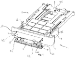
- Fig.1 shows an inventive chip card reader 1 in installation position in a spatial representation in a partially broken view from the top front.
- the retraction device 2 which has a stationary support member 3, in which a - here only partially visible - thrust element 4 is arranged movable back and forth.
- a folding element 5 is arranged in the front region, which is shown in its folded down by 90 ° position.
- a sealing element 6 is arranged positively.
- the folding element 5 is folded from its position shown by 90 ° to the front and moved backwards, so that the sealing element 6 rests against the front opening 17 of a housing front 7.
- the area 60 in which the sealing element 6 and the housing 8 are spaced from each other, is located in the lower - in the folded-down position in the rear - region of the folding element 5.
- the housing front. 7 closes the housing 8 towards the front. Both are shown here only partially and broken.
- a mounting hole 35 and snap hook 36 serve to attach the support member 2 to a printed circuit board, not shown here, which in turn is attached directly or indirectly to the housing 8.
- On the pusher 4 is a smart card 9, the front area is visible. It is supported in this area by two bars 41 of the pusher 4 down and stored by arranged at the front end retaining edges 42 from slipping out to the front.
- the chip card 9 is a multiple wider than the bars 41. Between the bar 41 is thus a large space within which a user grip the smart card 9 with two fingers, lift up over the retaining edge 42 and forward can pull out. It is also possible to lift the chip card 9 in the area between the two bars 41 by pressure from below beyond the holding edge 42. If, as provided according to a variant, the chip card 9 is arranged spring-loaded forward, it is moved after lifting over the retaining edge 42 also due to the spring force forward. It then protrudes even further forward beyond the front of the housing 7 and can thus be more easily gripped by the user. According to another variant, the chip card 9 is spring-loaded with a molded onto the thrust element 4 beam spring 40 forward.
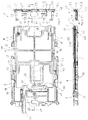
- Fig.2 shows the smart card reader 1 of Fig.1 in a partially broken top view from below.
- the same elements are provided with the same reference numerals and will generally be explained in more detail if further or different aspects than previously described arise.
- the retraction device 2 in which the thrust element 4 is in its retracted, retracted position with respect to the support member 3. It does not protrude forwards - in this illustration to the right - beyond the housing front 7.
- the housing 8 is here again only broken and partially shown to allow the view of the retraction device 2.
- the support element 3 has retaining arms 31, which are provided at their front end with inwardly projecting retaining lugs 32.
- stop elements 43 of the pusher element 4 cooperate with stop elements 43 of the pusher element 4, when this is moved from the position shown to the front - in the figure to the right. Once the stop members 43 abut against the retaining lugs 32, the pusher element 4 has reached its extended position and does not move further forward. In the retracted position of the push element 4 shown here, this is held by means of an edge 44 which bears against a release lever 34, not shown here. The edge 44 is located on a tongue 45.
- the thrust element 4 After loosening edge 44 and one not here represented unlocking lever 34 is moved to the right until it has reached its maximum extended position in which the stop members 43 abut against the retaining lugs 32.
- the unlocking lever 34 by which the edge 44 is held, is preferably movable by means of an electric actuator, for example by means of an electrically operated tension magnet. Once the release lever 34 is retracted, the push member 4 is moved to the right due to a spring bias.
- the release lever 34 no longer engage behind the edge 44, but lies laterally on the tongue 45 until, after insertion of the pusher element 4, it is again displaced to the left in the figure so far that the release lever 34, due to a spring preload, moves upward again in the illustration and engages behind the edge 44.
- the thrust element 4 has outwardly projecting guide lugs 48, 49, which interact with corresponding guide lugs 38, 39 of the carrier element 3. They serve for horizontal guidance of the push element. 4
- Figure 3 shows the section AA the Fig.2 , One recognizes the carrier element 3, under which the chip card 9 is located, which is mounted on the pusher element 4. On the left edge of the pusher member 4 can be seen whose tongue 45. On the right edge can be seen the housing 8 with the housing front 7, over which the folding element 5 does not extend in the retracted position shown.
- FIG 4 shows the enlarged right area of the Figure 3 , It can be seen that the front surface 51 of the folding element 5 does not protrude beyond the housing front 7 to the right.
- the sealing element 6 has a sealing lip 61, which seals up against the housing front 7 of the housing 8. Down the sealing element 6 is not on the front housing 7. Here is the spaced from the housing 8 area 60 of the sealing element 6.
- the sealing lip 61 extends over the entire width of the folding element and beyond even on the left and right vertical side. This is shown as a sealing lip 62 in one of the following figures. According to a variant of the invention, the sealing lip 61 terminates at the vertical sides approximately at the height in which the sealing element 6 ends in the illustrated section downwards. The spaced area 60 thus occupies the full width of the folding element 5.
- the sealing lip 61 extends downward in each case in an outer region, so that it seals the housing front 7 coming from the outer edges in this outer region also downwards. It then closes a less wide, spaced area 60th in, as shown here, sealing element 6 and housing front 7 are spaced down.
- this spaced-apart area 60 is relatively narrow and is bounded by another sealing area in the other direction.
- one or more spaced regions 60 may alternate with sealing regions. All these variants have in common that at the bottom of water or foreign substances, which are located in the region between the sealing lip 61 and front surface 51 in the upper and lateral areas, flow down and in the spaced area 60 through openings to the lowest area of the housing front. 7 can reach.
- This recess 14 is preferably a relatively wide gap. Variants provide that a plurality of narrow gaps or a plurality of bore-shaped recesses 14 are provided. All these variants have in common that they allow a connection of the interior of the housing 8 to the environment. In this way, both an air exchange take place, which serves to dissipate heat, as well as drain from above penetrated spray or condensate down.
- the folding element 5 has in its interior - in the Fig.linken - area a locking element 12. This engages upward beyond a projection 13 of the pusher element 4. In this way, the folding element 5 is held in its illustrated position, even if it is no longer held by the mechanical extension of the housing front 7 in this position after the extension of the thrust element 4 to the right. It can also be seen that the carrier element 3 in its front - right in the figure - area has a chamfer 33 which enables the smart card 9 in this area a certain mobility upwards, while otherwise only with little play down from support member 3 and thrust element 4 is held. Main function of the chamfer 33 is to facilitate the insertion of the smart card 9.
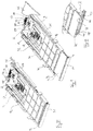
- Fig. 5 shows an enlarged top view from below, similar Fig. 2
- the folding element 5 from the front surface 51 in the figure to the left has extending arms 52, at the end of which inwardly facing pins 10 are located. These engage in holes 11 of the thrust element 4 and form the axis of rotation about which the folding element 5 can be folded down.
- the sealing element 6, which is sprayed flat behind the front surface 51 and is interrupted only by a few webs 53.
- the webs 53 connect the front surface 51 with rear parts of the folding element 5, for example the arms 52.
- the folding element 5 has a central part 54 which is provided with tongues 55 at the end of which the locking elements 12 are arranged.
- the sealing element 6 has a central part 64, which extends to the rear. It serves both for vibration damping of body vibrations in this area as well as folding down the folding element 5 down as a damping stop against the housing front 7.
- the central part 64 serves during manufacture as gate surface for the sealing element 6.
- the lateral sealing lips 62 which seal in this area against the housing front 7.
- the thrust element 4 can be further seen the projections 13, which cooperate in the mounted position of the folding element 5 with its locking elements 12.
- the thrust element 4 has stops 47, abut against the corresponding stops of the central part 54 of the folding element 5, when this is in its upper, unfolded position.
- the stops of the central part 54 are not visible because they are above, ie below the image plane shown here. In this position, the locking elements 12 and the projections 13 engage each other and hold the folding element 5 in the unfolded position.
- a spring tongue 46 which serves for fixing the chip card 9. On the other hand, it serves for pressing the chip card 9 to electrical contacts in order to ensure a secure electrical contact.
- a lowering mechanism is provided which lowers the pushing element in its retracted position in the direction of the electrical contacts. This is described in the following illustrations.
- the pins 10 are not round, but have a polygonal structure.
- the holes 11 in this case have a corrugated surface, which cooperates with the polygonal structure and serves to hold the folding element in its position.
- the polygonal structure is then a variant of the locking elements 12. It makes sense that the polygonal structure is designed so that they provide a solid support in the horizontal and folded down by 90 ° position. Under certain circumstances, two edges are sufficient.
- Figure 6 shows the section BB of Figure 5 , One recognizes the folding element 5 with front surface 51, the molded behind the front surface 51 positively sealing element 6 with sealing lip 61 and the central part 64.
- the central part 64 extends under the central part 54 of the folding element 5. Forward - in the figure to the right - closes the spaced area. A part of a web 53 is, as far as it is not covered by the sealing element 6, to recognize. In the left area of the folding element 5 is still a part of the arm 52 and the pin 10 can be seen.
- the carrier element 3 has a fastening hole 35.
- the carrier element 3 is fastened by means of a screw through the attachment hole 35 and two snap levers 36 on a printed circuit board of the housing 8, not shown here.
- the projection 13 and the stopper 47 In the right part of the pusher 4 can be seen the projection 13 and the stopper 47, to which a corresponding stop of the folding element 5 strikes when this assumes its upper, mounted position.
- Figure 7 shows the chip card reader the Fig.2 with extended thrust element 4. It can be seen the front of the housing 7 from below, the bars 41 of the outward - in the figure to the right - extended thrust element 4, the chip card mounted thereon 9 and the front surface 51 of the folded-down folding element 5.
- the lateral sealing lips 62nd and the upward sealing lip 61 are also visible.
- the stop elements 43 abut the retaining lugs 32 of the retaining arms 31.
- the spring tongue 46 exerts an upward pressure on the chip card 9.
- FIG 8 shows the section CC the Figure 7 , It can be seen the folded flap element 5 with sealing element 6, the central part 64 abuts against the housing front 7 dampening when the folding element 5 rotates when folding over the folded down by 90 ° position further out to the left.
- the smart card 9 is already in its front area - the right in the figure area - raised by the user up over the projection 13 and a piece far to the front - in the figure right - pulled out.
- the chip card 9 is bent upwards, which is facilitated by the chamfer 33 of the support member 3. Even in this position, the smart card 9 does not fall out of the smart card reader 1 by itself. For one thing, because she is prevented by the force exerted by the bending holding force on the projection 13 to a horizontal movement.
- the invention thus relates to a chip card reader 1 with a push element 4, on which a folding element 5 is arranged and into which a smart card 9 can be inserted.
- the sealing element 6 conducts water or condensed water or other foreign substances, which has penetrated from above, in the direction of the lower part of the housing 8.
- the chip card reader according to the invention it is easily possible to insert and remove the chip card 9.
- the proposed solution is inexpensive, allows the removal of heat from the interior and drainage of water from the inside out.
- the retraction device 2 of the chip card reader 1 has a carrier element 3 in which a movable thrust element 4 is arranged in front and back sliding. This is movable between a retracted position and an extended position.
- the folding element 5 has two pins 10, which are made of plastic and which are mounted in the front region of the thrust element 4 in holes 11. These fulfill the function of a joint.
- the flap member 5 which has two elastic latching elements 12, which are made of plastic, held in the horizontal position, since the latching elements 12 cooperate with projections 13 of the pusher 4.
- the thrust element 4 In order to remove the chip card 9 from the retraction device 2, the thrust element 4 must be in its extended position. Then the user folds down the folding element 5, the holding force of the locking elements 12 and projections 13, down from. Subsequently, the user has to lift the front end of the chip card 9 beyond the projections 13, which secure the chip card 9 in the push element 4.
- the folding element 5 has an elastic sealing element 6, which consists of a rubber material exists and in the closed state together with the front of the housing 7 about penetrated water towards the bottom of the housing 8 passes. Through the recess 14 in the bottom of the housing 8, this water is then passed out of the smart card reader 1.
- Figure 9 shows a smart card reader 1 in a spatial representation, similar to Fig.1 ,
- the support element 3 is fastened by means of its snap hooks 36 and the fastening hole 35 to a printed circuit board 21, which is only partially shown here.
- electrical contacts 22 are further attached, which serve to contact a contact pad 92 of the card 9.
- the contact field 92 is only partially visible in the pushed-out state of the push element 4 shown here.
- a switch 23 is further attached, the function of which is described in the following figures.
- a pull magnet 37 which cooperates with a release lever 34 is also attached to the circuit board 21.
- the snap hooks 36 have, unlike the snap hooks 36 shown in the preceding figures, a pyramidal shape, which facilitates insertion into corresponding holes of the printed circuit board 21.
- Figure 10 shows the chip card reader the Figure 9 with fold-down folding element 5. It can be seen the bar 41 with the holding edges 42, which have a rounded shape compared to the preceding figures. They are both rounded off to the side, and their upper edge is rounded in profile. This avoids both damage to the smart card 9 during removal and insertion, as well as possible injury to the user. In addition, the probability is reduced that foreign particles at the edges of the beams 41 and the Lock holding edges 42.
- the folding element 5 has recesses 56 which receive the front end of the beam 41 with the retaining edge 42 in the folded-up state.
- Figure 11 shows the chip card reader the Figure 9 with push element 4 in the retracted state.
- the contact field 92 of the chip card 9 is located below the electrical contacts 22.
- the chip card 9 is acted upon in this case by the spring tongue 46 so that a secure contact between the contacts 22 and the contact pad 92 is made.
- the thrust element 4 is displaced in its extremely retracted position in the vertical direction, thereby moving the chip card 9 with contact pad 92 toward the contacts 22. This is described in more detail in the following figures.
- compression springs 24 are biased more strongly in the retracted position of the thrust element 4 than in FIG Figure 9 shown. It can also be seen that the release lever 34 is moved further to the left and thereby engages behind the not visible here edge 44 of the tongue 45. A compression spring 27 of the tension magnet 37 is more relaxed than to Figure 9 shown. The pull magnet 37 is driven by electrical leads 25.
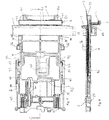
- Figure 12 shows a chip card reader in plan view from below.
- the drawn cut lines EE and DD do not run in a continuous line.
- the thrust element 4 with folded flap element 5 and sealing lip 62 of the sealing element 6.
- the guide lugs 48 which have an increase 481 in its end.
- a corresponding increase 482 in the front region of the guide lugs 48 is not visible here, since they are located in the figure below the guide lug 38.
- the guide tabs 38 have an increase 382 in their rear - left in the figure - area. This will be among the following Figures explained in more detail.
- the guide lugs 39 also have an elevation 392 in their rear area.
- Figure 13 shows the section DD of Figure 12 , It can be seen in the right area, the front surface 51, the sealing element 6 with upper sealing lip 61 and the front part of the smart card 9.
- the guide nose 48 of the pusher member 4 has at its retracted end of the increase 481 and at its front end, the increase 482. This is at the increase 382 of the guide nose 38 of the support member 3 at. It can be seen that in this position, the carrier element 3 is upwards - in the figure down - moved. In the left area can be seen the guide nose 39 with increase 392. At this is the increase 492 of the guide lug 49 at. Again, it can be seen that the thrust element 4 due to the interaction of the elevations 392 and 492 upwards - in the figure down - is shifted. The tongue 45 is still recognizable.
- Figure 14 shows the section EE the Figure 12 , In the right area can be seen the front surface 51 and the sealing element 6 with its upper sealing lip 62.
- the bar 41 with its holding edge 42 holds the smart card 9.
- the increase 482 of the guide nose 48 is present the increase 382 of the guide nose 38 at.
- the thrust element 4 and thus carried by this smart card 9 are thus shifted in this position of the thrust element 4 upwards.
- the increase 482 of the guide nose 48 which cooperates with an increase 392.
- the chip card 9 is thus also shifted upwards on this side, its contact field 92, which is located in the central region, is thus pressed against the electrical contacts 22, whereby a secure contact is ensured.
- the electrical leads 25 are shown for the pull magnet 37.
- Figure 15 shows the chip card reader the Figure 12 in the extended state of the pusher element 4.
- the cutting lines FF and GG do not run in a continuous line.
- the guide nose 38 with its increase 382 is compared to Figure 12 not shifted while the guide nose 48 is shifted to the right.
- Your increase 481 forms another stop on the increase 382, which is normally not needed.
- the elevation 482 is shifted far out of the region of the guide nose 38 to the right, the push element 4 is thus in its lowered position.
- the thrust element 4 is therefore lowered in this position.
- the compression springs 24 are relaxed after they have pushed the pusher 4 forward - in the figure to the right. This takes place as soon as the pull magnet 37 pulls the release lever 34 downwards in the illustration against the bias of the compression springs 27.
- the release lever disengages from the edge 44 and allows the displacement of the push element 4 to the right.
- the release lever 34 slides along the outside of the tongue 45 along.
- the arm 342 actuates the switch 23, which notifies a control unit, not shown, the unlocked state.
- the bar spring 40 presses the chip card 9 to the right against the retaining edge 42 (not shown here).
- the electrical contacts 22 and a switch 28 for the smart card 9 are visible in this position. The switch 28 is used to monitor whether a smart card 9 is inserted into the thrust element 4.
- Figure 16 shows the section FF the Figure 15 ,
- the front rounded corner of the smart card 9 is spaced from the sealing element 6, the upper sealing lip 62 is visible. It can also be seen here that the elevation 482 of the guide nose 48 is far away from the elevation 382 of the guide nose 38 of the carrier element 3. The same applies to the increase 492 of the guide nose 49 and the increase 392 of the guide nose 39.
- Fig. 17 shows the section GG the Fig. 15 ,
- the sealing element 6 with the upper sealing lip 62 is located between the bar and the front surface 51. Further to the left, it can be seen that the chip card 9 is spaced from the electrical contacts 22.
- the compression spring 24 can be seen in the relaxed state.
Landscapes
- Engineering & Computer Science (AREA)
- Artificial Intelligence (AREA)
- Computer Vision & Pattern Recognition (AREA)
- Physics & Mathematics (AREA)
- General Physics & Mathematics (AREA)
- Theoretical Computer Science (AREA)
- Credit Cards Or The Like (AREA)
- Coupling Device And Connection With Printed Circuit (AREA)
Abstract
Description
- Die vorliegende Erfindung betrifft ein Chipkartenlesegerät nach dem Oberbegriff des Anspruchs 1, eine Einfahrvorrichtung für ein solches Chipkartenlesegerät sowie ein Gerät welches ein Chipkartenlesegerät oder eine entsprechende Einfahrvorrichtung aufweist.
- Aus der
DE 103 39 931 A1 ist ein Chipkartenlesegerät mit abgedichteter Schublade bekannt. Aufgrund der Abdichtung bleibt die Chipkarte vor Wasser und anderen Fremdstoffen geschützt und ist im geschlossenen Zustand gegen die Umgebung abgeschottet. - Aufgabe der vorliegenden Erfindung ist es, ein demgegenüber verbessertes Chipkartenlesegerät vorzuschlagen.
- Erfindungsgemäß ist dazu ein Chipkartenlesegerät mit den Merkmalen des Anspruchs 1 vorgesehen.
- Das Chipkartenlesegerät weist ein Gehäuse auf, in dem ein eine Chipkarte aufnehmendes Schubelement zwischen einem eingefahrenen und einem ausgefahrenen Zustand vor- und zurückbeweglich angeordnet ist. Dabei ist die Chipkarte im eingefahrenen Zustand des Schubelements nicht entnehmbar. Das Schubelement ist im eingefahrenen Zustand mittels eines Dichtelements gegenüber dem Gehäuse abgedichtet. Das Dichtelement weist an zumindest einer Seite einen vom Gehäuse beabstandeten Bereich auf. Es ist also nicht komplett umlaufend abdichtend. Dies hat den Vorteil, einen Luftaustausch zwischen dem die Chipkarte umgebenden Bereich und der Umgebung zu ermöglichen und somit eine Überhitzung im Bereich der Chipkarte zu vermeiden.
- Erfindungsgemäß ist vorgesehen, dass sich der vom Gehäuse beabstandete Bereich in Einbaulage unten befindet. Eine Dichtlippe des Dichtelements liegt somit nur nach oben und seitlich komplett am Gehäuse an, während unten ein mehr oder weniger breiter Durchlass verbleibt. Dies ermöglicht den Abfluss von Spritz- oder Kondenswasser nach unten, welches sich vor dem Dichtelement im der Chipkarte abgewandten Bereich ansammeln kann, sodass es die Chipkarte nicht erreicht.
- Vorteilhafterweise ist das Dichtelement an einem Klappelement angeordnet. Der vor dem Dichtelement liegende Bereich wird durch Wegklappen des Klappelements im ausgefahrenen Zustand des Schubelements aus dem Bereich der Chipkarte entfernt. Eventuell dort noch befindliches Wasser oder Fremdstoffe sind dann weiter von der Chipkarte entfernt und können diese nicht oder nur unwesentlich beeinträchtigen.
- Erfindungsgemäß ist das Schubelement im Bereich des Klappelements durch einen Balken gebildet, dessen Breite nur einen Bruchteil der Breite der Chipkarte beträgt. Sinnvollerweise können hier auch zwei oder mehrere entsprechende Balken vorgesehen sein. Der oder die Balken stützen die Chipkarte ausreichend ab und ermöglichen es gleichzeitig, die Chipkarte zur Entnahme bzw. zum Einsetzen zu greifen.
- Gemäß einer vorteilhaften Ausgestaltung wird das Klappelement im ausgefahrenen Zustand des Schubelements in seiner Position gehalten, vorzugsweise durch Rastelemente. Die durch die Halterung definierte Stellung des Klappelements entspricht nach dem Ausfahren der selben wie im eingefahrenen Zustand und schützt die Chipkarte gegen ungewollte Entnahme. Erst wenn das Klappelement aktiv aus der gehaltenen Position herausbewegt wird, kann die Chipkarte entnommen und auch wieder eingesetzt werden.
- Das Schubelement weist vorteilhafterweise im Bereich des Dichtelements einer Haltekante auf, deren Ausdehnung in Richtung der Dicke der Chipkarte geringer ist, als die entsprechende Ausdehnung des Dichtelements. Dies erleichtert die Entnahme der Chipkarte, da sie nur geringfügig anzuheben ist um über die Haltekante hinweg herausgenommen werden zu können. Dabei tritt auch eine geringfügigere Verbiegung der Chipkarte auf als aus dem Stand der Technik bekannt. Eine längere Haltbarkeit aufgrund geringerer mechanischer Belastung der Chipkarte wird damit erzielt. Entsprechendes gilt für das Einsetzen der Chipkarte. Gleichzeitig wird das Dichtelement beim Einsetzen und Entnehmen der Karte geschont. Die Haltekante ist andererseits aber auch so hoch, dass die Chipkarte in der eingefahrenen Position des Schubelements weder entnehmbar noch einsetzbar ist, selbst wenn das Klappelement fehlerhafterweise entfernt oder nicht montiert sein sollte.
- Erfindungsgemäß ist das Dichtelement hinter einer Frontfläche des Klappelements flächig hinterspritzt. Dies hat den Vorteil einer guten Halterung am Klappelement durch die formschlüssige Verbindung zwischen Dichtelement und Frontfläche.
- Eine erfindungsgemäße Einfahrvorrichtung für ein Chipkartenlesegerät weist die genannten Vorteile des erfindungsgemäßen Chipkartenlesegeräts auf. Es kann auch ohne Gehäuse vertrieben werden und zeigt einige der erfindungsgemäßen Vorteile erst im Zusammenspiel mit dem entsprechenden Gehäuse.
- Ein Gerät mit einem erfindungsgemäßen Chipkartenlesegerät weist entsprechende Vorteile auf. Hierbei handelt es sich vorzugsweise um einen Tachographen oder ein anderes Gerät, bei dem Manipulationssicherheit von großer Wichtigkeit ist. Die erfindungsgemäße Lösung stellt sicher, dass die Chipkarte im eingefahrenen Zustand des Schubelements nicht entnehm- oder einsetzbar ist. Auch ein nach eventuellem Entfernen des Klappelements vorgenommener Versuch, die Chipkarte zu entnehmen, wird daran scheitern, dass die Balken eine Haltekante aufweisen. Ein Entfernen oder Einsetzen einer Chipkarte im eingefahrenen Zustand des Schubelements ist dann nur bei aktiver Entfernung der Haltekante möglich, welcher nachträglich detektierbar ist.
- Weitere Vorteile der Erfindung, Ausgestaltungen und Abwandlungen sind der nachfolgenden Beschreibung eines Ausführungsbeispiels entnehmbar. Dabei zeigen:
- Fig.1
- Chipkartenlesegerät in räumlicher Darstellung
- Fig.2
- Chipkartenlesegerät der
Fig.1 in teilweise gebrochener Draufsicht von unten - Fig.3
- Schnitt A-A der
Fig.2 - Fig.4
- vergrößerter rechter Bereich der
Fig.3 - Fig.5
- vergrößerte Draufsicht von unten mit separat dargestelltem Klappelement
- Fig.6
- Schnitt B-B der
Fig.5 - Fig.7
- Chipkartenlesegerät der
Fig.2 mit ausgefahrenem Schubelement - Fig.8
- Schnitt C-C der
Fig.7 - Fig.9
- Chipkartenlesegerät in räumlicher Darstellung
- Fig.10
- Chipkartenlesegerät in räumlicher Darstellung
- Fig.11
- Teil des Chipkartenlesegeräts der
Fig.10 - Fig.12
- Chipkartenlesegerät in Draufsicht von unten
- Fig.13
- Schnitt D-D der
Fig.12 - Fig.14
- Schnitt E-E der
Fig.12 - Fig.15
- Chipkartenlesegerät in Draufsicht von unten
- Fig.16
- Schnitt F-F der
Fig.15 - Fig.17
- Schnitt G-G der
Fig.15 -
Fig.1 zeigt ein erfindungsgemäßes Chipkartenlesegerät 1 in Einbaulage in räumlicher Darstellung in teilweise gebrochener Ansicht von vorne oben. Man erkennt die Einfahrvorrichtung 2, die ein ortsfestes Trägerelement 3 aufweist, in dem ein - hier nur teilweise sichtbares - Schubelement 4 vor- und zurückbeweglich angeordnet ist. Am Schubelement 4 ist in dessen vorderem Bereich ein Klappelement 5 angeordnet, welches in seiner um 90° nach unten abgeklappten Position gezeigt ist. Am Klappelement 5 ist ein Dichtelement 6 formschlüssig angeordnet. Im eingefahrenen Zustand des Schubelements 4 ist das Klappelement 5 von seiner dargestellten Stellung aus um 90° nach vorne hochgeklappt und nach hinten verschoben, sodass das Dichtelement 6 an der vorderen Öffnung 17 einer Gehäusefront 7 anliegt. Der Bereich 60, in dem Dichtelement 6 und Gehäuse 8 voneinander beabstandet sind, befindet sich im unteren - in der abgeklappten Position im hinteren - Bereich des Klappelements 5. Die Gehäusefront 7 schließt das Gehäuse 8 nach vorne hin ab. Beide sind hier nur teilweise und gebrochen dargestellt. Ein Befestigungsloch 35 und Schnapphaken 36 dienen der Befestigung des Trägerelements 2 an einer hier nicht dargestellten Leiterplatte, die wiederum direkt oder indirekt am Gehäuse 8 befestigt ist. Auf dem Schubelement 4 befindet sich eine Chipkarte 9, deren vorderer Bereich sichtbar ist. Sie wird in diesem Bereich von zwei Balken 41 des Schubelements 4 nach unten gestützt und durch an deren vorderem Ende angeordnete Haltekanten 42 vor einem Herausrutschen nach vorne bewahrt. - Man erkennt, dass die Chipkarte 9 um ein mehrfaches breiter ist, als die Balken 41. Zwischen den Balken 41 befindet sich somit ein großer Freiraum innerhalb dessen ein Nutzer die Chipkarte 9 mit zwei Fingern greifen, nach oben über die Haltekante 42 anheben und nach vorne herausziehen kann. Es ist ebenfalls möglich, die Chipkarte 9 im Bereich zwischen den beiden Balken 41 durch Druck von unten über die Haltekante 42 hinaus anzuheben. Wenn, wie nach einer Variante vorgesehen, die Chipkarte 9 nach vorne federbelastet angeordnet ist, wird sie nach dem Anheben über die Haltekante 42 hinaus aufgrund der Federkraft nach vorne verschoben. Sie ragt dann noch weiter nach vorne über die Gehäusefront 7 hinaus und lässt sich damit noch leichter vom Nutzer greifen. Gemäß einer anderen Variante ist die Chipkarte 9 mit einer an dem Schubelement 4 angespritzten Balkenfeder 40 nach vorne federbelastet. Dies dient nur zum Spielausgleich der Chipkarte 9 innerhalb ihrer Lagerung im Schubelement 4. Ein Vorspringen bei der Entnahme ist nach dieser Variante nicht vorgesehen. Zum Einsetzen der Chipkarte 9 wird diese über die Haltekanten 42 hinweg eingeschoben, bis ihr vorderes Ende die Haltekanten 42 passiert hat. Ihr hinteres Ende ist dabei dasjenige, das zuerst eingeschoben wird. Aufgrund einer nach unten gerichteten Kraft entlang der senkrechten Kante der Haltekante 42, die durch die Verbiegung der Chipkarte 9 beim Einschieben hervorgerufenen wird, rastet die Chipkarte 9 nach dem Passieren der Haltekanten 42 hinter diesen ein.
-
Fig.2 zeigt das Chipkartenlesegerät 1 derFig.1 in teilweise gebrochener Draufsicht von unten. Gleiche Elemente sind hier wie zu allen folgenden Figuren mit gleichen Bezugszeichen versehen und werden im allgemeinen dann näher erläutert, wenn sich weitere oder andere Aspekte als zuvor beschrieben ergeben. Man erkennt die Einfahrvorrichtung 2, in der sich das Schubelement 4 in seiner zurückbewegten, eingefahrenen Position bezüglich des Trägerelements 3 befindet. Es ragt nicht nach vorne - in dieser Abbildung nach rechts - über die Gehäusefront 7 hinaus. Das Gehäuse 8 ist auch hier wieder nur gebrochen und teilweise dargestellt, um den Blick auf die Einfahrvorrichtung 2 zu ermöglichen. Man erkennt, dass das Trägerelement 3 Haltearme 31 aufweist, die an ihrem vorderen Ende mit nach innen vorspringenden Haltenasen 32 versehen sind. Diese wirken mit Anschlagelementen 43 des Schubelements 4 zusammen, wenn dieses von der dargestellten Position aus nach vorne bewegt wird - in der Abbildung nach rechts. Sobald die Anschlagelemente 43 an die Haltenasen 32 anschlagen hat das Schubelement 4 seine ausgefahrene Position erreicht und bewegt sich nicht weiter nach vorne. In der hier dargestellten eingefahrenen Position des Schubelements 4 wird dieses mittels einer Kante 44 gehalten die an einem hier nicht dargestellten Entriegelungshebel 34 anliegt. Die Kante 44 befindet sich an einer Zunge 45. Über die Federkraft einer hier nicht dargestellten Feder, die in der dargestellten Position des Schubelements 4 auf dieses eine nach rechts gerichtete Kraft ausgeübt, wird das Schubelement 4 nach dem Lösen von Kante 44 und einem hier nicht dargestelltem Entriegelungshebel 34 nach rechts bewegt, bis es seine maximal ausgefahrenen Position erreicht hat, in der die Anschlagelemente 43 an die Haltenasen 32 anschlagen. Der Entriegelungshebel 34, durch den die Kante 44 gehalten wird, ist vorzugsweise mittels eines elektrischen Aktuators bewegbar, beispielsweise mittels eines elektrisch betätigten Zugmagneten. Sobald der Entriegelungshebel 34 zurückgezogen ist, wird das Schubelement 4 aufgrund einer Federvorspannung nach rechts bewegt. Auch wenn der Zugmagnet nicht mehr aktiv ist kann der Entriegelungshebel 34 dann nicht mehr hinter die Kante 44 einrasten, sondern liegt seitlich an der Zunge 45 an, bis diese, nach Einschieben des Schubelements 4, wieder so weit nach in der Abbildung links verschoben ist, dass der Entriegelungshebel 34 aufgrund einer Federvorspannung sich wieder in der Abbildung nach oben bewegt und hinter der Kante 44 einrastet. - Das Schubelement 4 weist nach außen vorstehende Führungsnasen 48,49 auf, die mit entsprechenden Führungsnasen 38,39 des Trägerelements 3 zusammenwirken. Sie dienen zur horizontalen Führung des Schubelements 4.
-
Fig.3 zeigt den Schnitt A-A derFig.2 . Man erkennt das Trägerelement 3, unter dem sich die Chipkarte 9 befindet, die auf dem Schubelement 4 gelagert ist. Am linken Rand des Schubelements 4 erkennt man dessen Zunge 45. Am rechten Rand erkennt man das Gehäuse 8 mit Gehäusefront 7, über die das Klappelement 5 in der dargestellten eingezogenen Position nicht hinausreicht. -
Fig.4 zeigt den vergrößerten rechten Bereich derFig.3 . Man erkennt, dass die Frontfläche 51 des Klappelements 5 nicht über die Gehäusefront 7 nach rechts hinausragt. Das Dichtelement 6 weist eine Dichtlippe 61 auf, die nach oben gegen die Gehäusefront 7 des Gehäuses 8 abdichtet. Nach unten liegt das Dichtelement 6 nicht an der Gehäusefront 7 an. Hier befindet sich der vom Gehäuse 8 beabstandete Bereich 60 des Dichtelements 6. Die Dichtlippe 61 erstreckt sich über die gesamte Breite des Klappelements und darüber hinaus auch noch auf der linken und rechten senkrechten Seite. Dies ist in einer der folgenden Abbildungen als Dichtlippe 62 gezeigt. Gemäß einer Variante der Erfindung endet die Dichtlippe 61 an den senkrechten Seiten in etwa auf der Höhe, in der das Dichtelement 6 im dargestellten Schnitt nach unten endet. Der beabstandete Bereich 60 nimmt somit die volle Breite des Klappelements 5 ein. Gemäß einer anderen Variante verläuft die Dichtlippe 61 auch nach unten in jeweils einem äußeren Bereich, sodass sie von den Außenkanten her kommend in diesem äußeren Bereich auch nach unten hin die Gehäusefront 7 abdichtet. Es schließt sich dann ein weniger breiter, beabstandeter Bereich 60 an, in dem, wie hier dargestellt, Dichtelement 6 und Gehäusefront 7 nach unten beabstandet sind. Gemäß einer Variante ist dieser beabstandete Bereich 60 relativ schmal und wird von einem weiteren abdichtenden Bereich in die andere Richtung begrenzt. Gemäß einer Variante können sich einer oder mehrere beabstandete Bereiche 60 mit abdichtenden Bereichen abwechseln. Allen diesen Varianten ist gemeinsam, dass im unteren Bereich Wasser oder Fremdstoffe, die sich im Bereich zwischen Dichtlippe 61 und Frontfläche 51 in deren oberen und seitlichen Bereichen befinden, nach unten abfließen und im beabstandeten Bereich 60 durch Öffnungen bis in den untersten Bereich der Gehäusefront 7 gelangen können. Dort befindet sich eine Ausnehmung 14, über die das dahin abgeleitete Wasser und Fremdstoffe aus dem Gehäuse 8 hinaus gelangen können. Diese Ausnehmung 14 ist vorzugsweise ein relativ breiter Spalt. Varianten sehen vor, dass mehrere schmale Spalte oder mehrere bohrungsförmige Ausnehmungen 14 vorgesehen sind. Allen diesen Varianten ist gemeinsam, dass sie eine Verbindung des Innenraums des Gehäuses 8 zur Umgebung ermöglichen. Auf diese Weise kann sowohl ein Luftaustausch stattfinden, der zur Wärmeabfuhr dient, als auch von oben eingedrungenes Spritzwasser oder Kondenswasser nach unten abfließen. - Das Klappelement 5 weist in seinem Inneren - in der Fig.linken - Bereich ein Rastelement 12 auf. Dieses greift nach oben über einen Vorsprung 13 des Schubelements 4 hinaus. Auf diese Weise wird das Klappelement 5 in seiner dargestellten Position gehalten, auch wenn es nach dem Ausfahren des Schubelements 4 nach rechts nicht mehr durch mechanische Anlage an der Gehäusefront 7 in dieser Position gehalten wird. Man erkennt weiterhin, dass das Trägerelement 3 in seinem vorderen - in der Abbildung rechten - Bereich eine Abschrägung 33 aufweist die der Chipkarte 9 in diesem Bereich eine gewisse Beweglichkeit nach oben ermöglicht, während sie ansonsten nur mit wenig Spiel nach unten von Trägerelement 3 und Schubelement 4 gehalten wird. Hauptfunktion der Abschrägung 33 ist es, das Einführen der Chipkarte 9 zu erleichtern.
-
Fig. 5 zeigt eine vergrößerte Draufsicht von unten, ähnlichFig. 2 , mit separat dargestelltem Klappelement 5 und ohne Darstellung von Gehäusefront 7 oder Gehäuse 8. Man erkennt, dass das Klappelement 5 von der Frontfläche 51 in der Abbildung nach links sich erstreckende Arme 52 aufweist, an deren Ende sich nach innen weisende Stifte 10 befinden. Diese greifen in Löcher 11 des Schubelements 4 ein und bilden die Drehachse, um die sich das Klappelement 5 abklappen lässt. Man erkennt weiterhin das Dichtelement 6, das flächig hinter die Frontfläche 51 verspritzt ist und nur von wenigen Stegen 53 unterbrochen wird. Die Stege 53 verbinden die Frontfläche 51 mit rückwärtigen Teilen des Klappelements 5, beispielsweise den Armen 52. Im mittleren Bereich weist das Klappelement 5 ein Zentralteil 54 auf, welches mit Zungen 55 versehen ist, an deren Ende die Rastelemente 12 angeordnet sind. Auch das Dichtelement 6 weist ein Zentralteil 64 auf, welches sich nach hinten erstreckt. Es dient sowohl zur Schwingungsdämpfung von Körperschwingungen in diesem Bereich als auch beim Abklappen des Klappelements 5 nach unten als dämpfender Anschlag gegen die Gehäusefront 7. Außerdem dient das Zentralteil 64 während der Herstellung als Angußfläche für das Dichtelement 6. Im in der Abbildung oberen und unteren Bereich erkennt man die seitlichen Dichtlippen 62, die in diesem Bereich gegen die Gehäusefront 7 abdichten. Am Schubelement 4 erkennt man weiterhin die Vorsprünge 13, die in montierter Position des Klappelements 5 mit dessen Rastelementen 12 zusammenwirken. Das Schubelement 4 weist Anschläge 47 auf, an die entsprechende Anschläge des Zentralteils 54 des Klappelements 5 anschlagen, wenn sich dieses in seiner oberen, nicht abgeklappten Position befindet. In der hier gewählten Darstellung sind die Anschläge des Zentralteils 54 nicht sichtbar, da sie sich oben, also unterhalb der hier gezeigten Bildebene befinden. In dieser Position greifen die Rastelemente 12 und die Vorsprünge 13 ineinander und halten das Klappelement 5 in der nicht-abgeklappten Position. Im linken Bereich des Schubelements 4 erkennt man eine Federzunge 46 die zum einen zur Fixierung der Chipkarte 9 dient. Zum anderen dient sie zum Anpressen der Chipkarte 9 an elektrische Kontakte, um einen sicheren elektrischen Kontakt zu gewährleisten. - Gemäß einer Variante ist statt einer Federzunge 46 ein Absenkmechanismus vorgesehen, der das Schubelement in seiner eingefahrenen Position in Richtung auf die elektrischen Kontakte hin absenkt. Dies ist zu folgenden Abbildungen beschrieben.
- Gemäß einer Variante sind die Stifte 10 nicht rund ausgebildet, sondern weisen eine Mehrkantstruktur auf. Die Löcher 11 weisen dabei eine geriffelte Oberfläche auf, die mit der Mehrkantstruktur zusammenwirkt und dazu dient das Klappelement in seiner Position zu halten. Die Mehrkantstruktur ist dann eine Variante der Rastelemente 12. Sinnvollerweise ist die Mehrkantstruktur so ausgebildet, dass sie eine feste Halterung in der waagrechten und der um 90° nach unten abgeklappten Position bieten. Dazu reichen unter Umständen zwei Kanten aus.
-
Fig.6 zeigt den Schnitt B-B derFig.5 . Man erkennt das Klappelement 5 mit Frontfläche 51, das hinter der Frontfläche 51 formschlüssig angespritzte Dichtelement 6 mit Dichtlippe 61 und das Zentralteil 64. Das Zentralteil 64 erstreckt sich unter dem Zentralteil 54 des Klappelements 5. Nach vorne - in der Abbildung nach rechts - schließt sich der beabstandete Bereich an. Ein Teil eines Stegs 53 ist, soweit er nicht vom Dichtelement 6 verdeckt ist, zu erkennen. Im linken Bereich des Klappelements 5 sind noch ein Teil des Arms 52 und der Stift 10 erkennbar. - Im linken Teil der
Fig.6 erkennt man das Schubelement 4 auf welchem die Chipkarte 9 aufliegt. Im in der Abbildung rechten Teil des Schubelements 4 liegt die Chipkarte 9 nicht mehr komplett auf sondern nur noch auf den Balken 41. Die Chipkarte 9 wird von deren Haltekante 42 am Herausfallen nach vorne - in der Abbildung nach rechts - gehindert. Die Haltekante 42 verriegelt die Chipkarte 9 auch dann, wenn im eingefahrenen Zustand des Schubelements 4 das Klappelement 5 demontiert sein sollte. Man erkennt, dass die Haltekante 42 sich weniger weit nach oben erstreckt als die Dichtlippe 61 des Dichtelements 6. Im linken Bereich des Schubelements 4 weist dieses eine nach oben gebogene Federzunge 46 auf, welche gegen die Chipkarte 9 eine nach oben gerichtete Kraft ausübt. Durch diese Kraft wird die Chipkarte 9 zum einen auch in diesem Bereich gegen Verschieben gesichert. Zum anderen dient dies zum sicheren Kontaktieren von in diesem Bereich im eingefahrenen Zustand befindlichen elektrischen Kontakten mit einem Kontaktfeld der Chipkarte 9. Das Trägerelement 3 weist ein Befestigungsloch 35 auf. Das Trägerelement 3 wird mittels einer Schraube durch das Befestigungsloch 35 und zweier Schnapphebel 36 an einer hier nicht dargestellten Leiterplatte des Gehäuses 8 befestigt. Im rechten Teil des Schubelements 4 erkennt man den Vorsprung 13 und den Anschlag 47, an den ein entsprechender Anschlag des Klappelements 5 anschlägt wenn dieses seine obere, montierte Position einnimmt. -
Fig.7 zeigt das Chipkartenlesegerät derFig.2 mit ausgefahrenem Schubelement 4. Man erkennt die Gehäusefront 7 von unten, die Balken 41 des nach außen - in der Abbildung nach rechts - ausgefahrenen Schubelements 4, die darauf gelagerte Chipkarte 9 und die Frontfläche 51 des nach unten abgeklappten Klappelements 5. Die seitlichen Dichtlippen 62 und die nach oben abdichtende Dichtlippe 61 sind ebenfalls erkennbar. Im mittleren Teil der Abbildung erkennt man, dass die Anschlagelemente 43 an den Haltenasen 32 der Haltearme 31 anschlagen. Die Federzunge 46 übt einen nach oben gerichteten Druck auf die Chipkarte 9 aus. -
Fig.8 zeigt den Schnitt C-C derFig.7 . Man erkennt das abgeklappte Klappelement 5 mit Dichtelement 6, dessen Zentralteil 64 gegen die Gehäusefront 7 dämpfend anschlägt wenn das Klappelement 5 sich beim Abklappen über die um 90° nach unten abgeklappte Position hinaus weiter nach links dreht. Die Chipkarte 9 ist bereits in ihrem vorderen Bereich - dem in der Abbildung rechten Bereich - vom Nutzer nach oben über den Vorsprung 13 hinaus angehoben und ein Stück weit nach vorne - in der Abbildung rechts - herausgezogen. Die Chipkarte 9 wird dabei nach oben gebogen, was durch die Abschrägung 33 des Trägerelements 3 erleichtert wird. Auch in dieser Position fällt die Chipkarte 9 nicht von alleine aus dem Chipkartenlesegerät 1 heraus. Zum einen weil sie durch die von der Verbiegung ausgeübten Haltekraft auf den Vorsprung 13 an einer Horizontalbewegung gehindert ist. Zum anderen auch weil sie von der Federzunge 46 des Schubelements 4 in ihrem hinteren Bereich beaufschlagt wird. Der Nutzer muss die Chipkarte 9 aktiv greifen und bewegen, um sie zu entnehmen. Beim Einschieben der Chipkarte 9 wird deren Bewegung abgebremst, sobald sie den Bereich der Federzunge 46 erreicht. - Die Erfindung betrifft also ein Chipkartenlesegerät 1 mit einem Schubelement 4, an dem ein Klappelement 5 angeordnet ist und in das eine Chipkarte 9 einlegbar ist. Das Dichtelement 6 leitet etwa von oben eingedrungenes Wasser oder Kondenswasser oder andere Fremdstoffe Richtung unterem Teil des Gehäuses 8. Mit dem erfindungsgemäßen Chipkartenlesegerät ist es einfach möglich, die Chipkarte 9 zu einzusetzen und wieder zu entnehmen. Die vorgeschlagene Lösung ist kostengünstig, ermöglicht die Abfuhr von Wärme aus dem Innenbereich sowie einen Abfluss von Wasser aus dem Innenbereich heraus. Die Einfahrvorrichtung 2 des Chipkartenlesegeräts 1 hat ein Trägerelement 3 in dem vor- und zurückgleitend ein bewegliches Schubelement 4 angeordnet ist. Dieses ist zwischen einer eingefahrenen und einer ausgefahrenen Position beweglich. Das Klappelement 5 hat zwei Stifte 10, die aus Kunststoff bestehen und die im vorderen Bereich des Schubelements 4 in Löchern 11 gelagert sind. Diese erfüllen die Funktion eines Gelenks. Wenn das Schubelement 4 sich in seiner ausgefahrenen Position befindet, wird das Klappelement 5, das zwei elastische Rastelemente 12 aufweist, die aus Kunststoff bestehen, in der horizontalen Position gehalten, da die Rastelemente 12 mit Vorsprüngen 13 des Schubelements 4 zusammenwirken. Um die Chipkarte 9 aus der Einfahrvorrichtung 2 zu entnehmen muss sich das Schubelement 4 in seiner ausgefahrenen Position befinden. Dann klappt der Nutzer das Klappelement 5, die Haltekraft der Rastelemente 12 und Vorsprünge 13 überwindend, nach unten ab. Anschließend muss der Nutzer das vordere Ende der Chipkarte 9 über die Vorsprünge 13 hinaus anheben, die die Chipkarte 9 im Schubelement 4 sichern. Das Klappelement 5 weist ein elastisches Dichtelement 6 auf, welches aus einem Gummimaterial besteht und im geschlossenen Zustand zusammen mit der Gehäusefront 7 etwa eingedrungenes Wasser Richtung Boden des Gehäuses 8 leitet. Durch die Ausnehmung 14 im Boden des Gehäuses 8 wird dieses Wasser dann aus dem Chipkartenlesegerät 1 hinausgeleitet.
-
Fig.9 zeigt ein Chipkartenlesegerät 1 in räumlicher Darstellung, ähnlich zuFig.1 . Man erkennt die Chipkarte 9, die Frontfläche 51 mit dahinterliegendem Dichtelement 6, und das Trägerelement 3 mit Haltearmen 31. Das Trägerelement 3 ist mittels seiner Schnapphaken 36 und dem Befestigungsloch 35 an einer Leiterplatte 21 befestigt, die hier nur sehr teilweise dargestellt ist. An der Leiterplatte 21 sind weiterhin elektrische Kontakte 22 befestigt, die zum Kontaktieren eines Kontaktfelds 92 der Karte 9 dienen. Das Kontaktfeld 92 ist in dem hier dargestellten herausgeschobenen Zustand des Schubelements 4 nur teilweise sichtbar. An der Leiterplatte 21 ist weiterhin ein Schalter 23 befestigt, dessen Funktion zu nachfolgenden Abbildungen beschrieben wird. Ein Zugmagnet 37, der mit einem Entriegelungshebel 34 zusammenwirkt ist ebenfalls an der Leiterplatte 21 befestigt. Man erkennt weiterhin Druckfedern 24, die das Schubelement 4 gegen das Trägerelement 3 in seine dargestellte herausgefahrene Position schieben. Die Schnapphaken 36 weisen, anders als die zu den vorhergehenden Abbildungen gezeigten Schnapphaken 36, eine pyramidenartige Form auf, welche das Einsetzen in entsprechende Löcher der Leiterplatte 21 erleichtert. -
Fig.10 zeigt das Chipkartenlesegerät derFig.9 mit abgeklapptem Klappelement 5. Man erkennt die Balken 41 mit den Haltekanten 42, die gegenüber den vorhergehenden Abbildungen eine abgerundete Form aufweisen. Dabei sind sie sowohl seitlich abgerundet, als auch ist ihre obere Kante im Profil abgerundet. Dies vermeidet sowohl Beschädigungen der Chipkarte 9 beim Entnehmen und Einschieben, als auch mögliche Verletzungen des Nutzers. Außerdem wird die Wahrscheinlichkeit gemindert, dass sich Fremdpartikel an den Kanten der Balken 41 beziehungsweise der Haltekanten 42 festsetzen. Das Klappelement 5 weist Aussparungen 56 auf, die im hochgeklappten Zustand das vordere Ende der Balken 41 mit der Haltekante 42 aufnehmen. -
Fig.11 zeigt das Chipkartenlesegerät derFig.9 mit Schubelement 4 im eingefahrenen Zustand. Das Kontaktfeld 92 der Chipkarte 9 befindet sich unterhalb der elektrischen Kontakte 22. Die Chipkarte 9 ist in diesem Fall durch die Federzunge 46 so beaufschlagt, dass ein sicherer Kontakt zwischen den Kontakten 22 und dem Kontaktfeld 92 besteht. Alternativ zur Federzunge 46 ist vorgesehen, dass das Schubelement 4 in seiner äußerst eingefahrenen Position in vertikaler Richtung verschoben wird und dadurch die Chipkarte 9 mit Kontaktfeld 92 auf die Kontakte 22 zubewegt wird. Dies wird zu den folgenden Abbildungen näher beschrieben. - Man erkennt, dass die Druckfedern 24 in der eingefahrenen Position des Schubelements 4 stärker vorgespannt sind als in
Fig.9 gezeigt. Man erkennt weiterhin, dass der Entriegelungshebel 34 weiter nach links verschoben ist und dabei hinter der hier nicht sichtbaren Kante 44 der Zunge 45 einrastet. Eine Druckfeder 27 des Zugmagneten 37 ist dabei entspannter als zuFig.9 gezeigt. Der Zugmagnet 37 wird über elektrische Zuleitungen 25 angesteuert. -
Fig.12 zeigt ein Chipkartenlesegerät in Draufsicht von unten. Die eingezeichneten Schnittlinien E-E und D-D verlaufen, wie eingezeichnet, nicht in einer durchgehenden Linie. Man erkennt das Schubelement 4 mit hochgeklapptem Klappelement 5 und Dichtlippe 62 des Dichtelements 6. Man erkennt weiterhin die Führungsnasen 48, die in ihrem Endbereich eine Erhöhung 481 aufweisen. Eine entsprechende Erhöhung 482 im vorderen Bereich der Führungsnasen 48 ist hier nicht sichtbar, da sie sich in der Abbildung unter der Führungsnase 38 befinden. Auch die Führungsnasen 38 weisen eine Erhöhung 382 in ihrem hinteren - in der Abbildung linken - Bereich auf. Dies wird zu den nachfolgenden Abbildungen näher erläutert. Auch die Führungsnasen 39 weisen eine Erhöhung 392 in ihrem hinteren Bereich auf. - Im linken Bereich der
Fig.12 erkennt man, dass hier keine Federzunge 46 wie zu den vorhergehenden Abbildungen beschrieben vorgesehen ist. Stattdessen wird das Schubelement 4 in seiner hinteren Position angehoben. Man erkennt weiterhin den Zugmagneten 37 mit seinen elektrischen Zuleitungen 25, der mittels einer Druckfeder 27 vorgespannt ist und mit einer Frontscheibe 30 versehen ist, die in eine Ausnehmung 341 des Entriegelungshebels 34 eingreift. Der Entriegelungshebel 34 befindet sich aufgrund der Vorspannung durch die Druckfeder 27 in seiner vorgeschobenen Position, in der er hinter die Kante 44 der Zunge 45 greift und somit das Schubelement 4 gegen ein Verschieben nach außen verriegelt. Ein Arm 342 des Entriegelungshebels 34 ist in dieser Position vom Schalter 23 beabstandet. Dieser ist damit nicht betätigt. -
Fig.13 zeigt den Schnitt D-D derFig.12 . Man erkennt im rechten Bereich die Frontfläche 51, das Dichtelement 6 mit oberer Dichtlippe 61 und den vorderen Teil der Chipkarte 9. Die Führungsnase 48 des Schubelements 4 weist an ihrem eingezogenen Ende die Erhöhung 481 auf und an ihrem vorderen Ende die Erhöhung 482. Diese liegt an der Erhöhung 382 der Führungsnase 38 des Trägerelements 3 an. Man erkennt, dass in dieser Position das Trägerelement 3 nach oben - in der Abbildung nach unten - verschoben ist. Im linken Bereich erkennt man die Führungsnase 39 mit Erhöhung 392. An dieser liegt die Erhöhung 492 der Führungsnase 49 an. Auch hier erkennt man, dass das Schubelement 4 aufgrund des Zusammenwirkens der Erhöhungen 392 und 492 nach oben - in der Abbildung nach unten - verschoben ist. Man erkennt weiterhin die Zunge 45. -
Fig.14 zeigt den Schnitt E-E derFig.12 . Im rechten Bereich erkennt man die Frontfläche 51 und das Dichtelement 6 mit seiner oberen Dichtlippe 62. Der Balken 41 mit seiner Haltekante 42 hält die Chipkarte 9. Die Erhöhung 482 der Führungsnase 48 liegt an der Erhöhung 382 der Führungsnase 38 an. Das Schubelement 4 und damit die von diesem getragene Chipkarte 9 sind somit in dieser Position des Schubelements 4 nach oben verschoben. Im linken Bereich erkennt man die Erhöhung 482 der Führungsnase 48, die mit einer Erhöhung 392 zusammenwirkt. Die Chipkarte 9 ist somit auch auf dieser Seite nach oben verschoben, ihr Kontaktfeld 92, welches sich im mittleren Bereich befindet, ist somit gegen die elektrischen Kontakte 22 gedrückt wodurch eine sichere Kontaktierung gewährleistet ist. Ganz links sind die elektrischen Zuleitungen 25 für den Zugmagneten 37 gezeigt. -
Fig.15 zeigt das Chipkartenlesegerät derFig.12 im ausgefahrenen Zustand des Schubelements 4. Auch hier verlaufen die Schnittlinien F-F und G-G nicht in einer durchlaufenden Linie. Die Führungsnase 38 mit ihrer Erhöhung 382 ist im Vergleich zuFig.12 nicht verschoben, während die Führungsnase 48 nach rechts verschoben ist. Ihre Erhöhung 481 bildet einen weiteren Anschlag an der Erhöhung 382, der im Normalfall nicht benötigt wird. Die Erhöhung 482 ist weit aus dem Bereich der Führungsnase 38 nach rechts verschoben, das Schubelement 4 befindet sich somit in seiner abgesenkten Position. Ähnliches gilt im Bereich der Führungsnase 39, die nun nichtmehr mit der Erhöhung 492 der Führungsnase 49 des Schubelements 4 in Kontakt steht. Das Schubelement 4 ist also auch in dieser Position abgesenkt. Man erkennt weiterhin, dass die Druckfedern 24 entspannt sind, nachdem sie das Schubelement 4 nach vorne - in der Abbildung nach rechts - verschoben haben. Dies erfolgt, sobald der Zugmagnet 37 gegen die Vorspannung der Druckfedern 27 den Entriegelungshebel 34 in der Abbildung nach unten zieht. Dabei rastet der Entriegelungshebel aus der Kante 44 aus und ermöglicht das Verschieben des Schubelements 4 nach rechts. Der Entriegelungshebel 34 gleitet dabei an der Außenseite der Zunge 45 entlang. Außerdem betätigt der Arm 342 den Schalter 23, der einer nicht dargestellten Steuerungseinheit den entriegelten Zustand mitteilt. Man erkennt weiterhin, dass die Balkenfeder 40 die Chipkarte 9 nach rechts gegen die Haltekante 42 (hier nicht dargestellt) drückt. Auch die elektrischen Kontakte 22 und ein Schalter 28 für die Chipkarte 9 sind in dieser Position sichtbar. Der Schalter 28 dient zur Überwachung ob eine Chipkarte 9 in das Schubelement 4 eingelegt ist. - Eingezeichnet ist hier auch die Vor-Zurück-Bewegungsrichtung 400 des Schubelements 4 sowie gestrichelt eine senkrecht auf dieser stehende Ebene 401. Man erkennt, dass in dieser Ebene 401 die Dichtlippen 62 liegen. Ebenso liegt die hier nicht sichtbare Dichtlippe 61 in der Ebene 401. Nach unten - in der Abbildung nach oben - anschließend liegt der Bereich 60, in dem das Dichtelement 6 keine Dichtlippe aufweist. Die Ebene 401 ist auch sich in die anschließenden Abbildungen
Fig.16 und Fig.17 erstreckend eingezeichnet. -
Fig.16 zeigt den Schnitt F-F derFig.15 . Die vordere abgerundete Ecke der Chipkarte 9 ist vom Dichtelement 6 beabstandet, dessen obere Dichtlippe 62 sichtbar ist. Man sieht auch hier, dass die Erhöhung 482 der Führungsnase 48 weit von der Erhöhung 382 der Führungsnase 38 des Trägerelements 3 entfernt ist. Entsprechendes gilt für die Erhöhung 492 der Führungsnase 49 und die Erhöhung 392 der Führungsnase 39. -
Fig. 17 zeigt den Schnitt G-G derFig. 15 . Man erkennt die Chipkarte 9, die an der Haltekante 42 des Balkens 41 vorne anliegt. Das Dichtelement 6 mit oberer Dichtlippe 62 befindet sich zwischen Balken und Frontfläche 51. Weiter links erkennt man, dass die Chipkarte 9 von den elektrischen Kontakten 22 beabstandet ist. Die Druckfeder 24 ist im entspannten Zustand erkennbar.
Claims (9)
- Chipkartenlesegerät (1) mit einem Gehäuse (8), in dem ein eine Chipkarte (9) aufnehmendes Schubelement (4) zwischen einem eingefahrenen und einem ausgefahrenen Zustand vor- und zurückbeweglich angeordnet ist, die Chipkarte (9) im eingefahrenen Zustand des Schubelements (4) nicht entnehmbar ist, und das Schubelement (4) im eingefahrenen Zustand mittels eines Dichtelements (6) abgedichtet ist,
dadurch gekennzeichnet, dass das Dichtelement (6) im eingefahrenen Zustand des Schubelements (4) an zumindest einer Seite einen vom Gehäuse (8) beabstandeten Bereich (60) aufweist. - Chipkartenlesegerät nach Anspruch 1, dadurch gekennzeichnet, dass sich der vom Gehäuse (8) beabstandete Bereich (60) in Einbaulage unten befindet.
- Chipkartenlesegerät nach einem der vorhergehenden Ansprüche, dadurch gekennzeichnet, dass das Dichtelement (6) an einem Klappelement (5) angeordnet ist.
- Chipkartenlesegerät nach einem der vorhergehenden Ansprüche, dadurch gekennzeichnet, dass das Schubelement (4) im Bereich des Klappelements (5) aus zumindest einem Balken (41) gebildet ist, dessen Breite nur einen Bruchteil der Breite der Chipkarte (9) beträgt.
- Chipkartenlesegerät nach einem der vorhergehenden Ansprüche, dadurch gekennzeichnet, dass das Klappelement (5) im ausgefahrenen Zustand des Schubelements (4) mittels Rastelementen (12) in seiner Position gehalten wird.
- Chipkartenlesegerät nach einem der vorhergehenden Ansprüche, dadurch gekennzeichnet, dass das Schubelement (4) im Bereich des Dichtelements (6) eine Haltekante (42) aufweist, deren Ausdehnung in Richtung der Dicke der Chipkarte (9) geringer ist, als die entsprechende Ausdehnung des Dichtelements (6).
- Chipkartenlesegerät nach einem der vorhergehenden Ansprüche, dadurch gekennzeichnet, dass das Dichtelement (6) hinter einer Frontfläche (51) des Klappelements (5) flächig hinterspritzt ist.
- Einfahrvorrichtung (2) für ein Chipkartenlesegerät (1), aufweisend ein eine Chipkarte (9) aufnehmendes Schubelement (4) welches zwischen einem eingefahrenen und einem ausgefahrenen Zustand vor- und zurückbeweglich angeordnet ist, die Chipkarte (9) im eingefahrenen Zustand des Schubelements (4) nicht entnehmbar ist, und das Schubelement (4) ein Dichtelement (6) aufweist, dadurch gekennzeichnet, dass das Dichtelement (6) in einer senkrecht zur Vor-Zurück-Bewegungsrichtung (400) des Schubelements (4) stehenden Ebene (401) sowohl zumindest einen Bereich mit Dichtlippe (61, 62) als auch zumindest einen Bereich (60) ohne Dichtlippe aufweist.
- Gerät mit einem Chipkartenlesegerät (1) oder einer Einfahrvorrichtung (2) gemäß einem der vorhergehenden Ansprüche.
Applications Claiming Priority (1)
| Application Number | Priority Date | Filing Date | Title |
|---|---|---|---|
| DE102016214180.5A DE102016214180A1 (de) | 2016-08-01 | 2016-08-01 | Chipkartenlesegerät |
Publications (2)
| Publication Number | Publication Date |
|---|---|
| EP3279827A1 true EP3279827A1 (de) | 2018-02-07 |
| EP3279827B1 EP3279827B1 (de) | 2020-06-24 |
Family
ID=59362977
Family Applications (1)
| Application Number | Title | Priority Date | Filing Date |
|---|---|---|---|
| EP17181429.6A Active EP3279827B1 (de) | 2016-08-01 | 2017-07-14 | Chipkartenlesegerät |
Country Status (2)
| Country | Link |
|---|---|
| EP (1) | EP3279827B1 (de) |
| DE (1) | DE102016214180A1 (de) |
Citations (4)
| Publication number | Priority date | Publication date | Assignee | Title |
|---|---|---|---|---|
| DE3916783A1 (de) * | 1988-10-19 | 1990-04-26 | Landis & Gyr Ag | Vorrichtung zum lesen und/oder beschreiben von chip-karten |
| DE10339931A1 (de) | 2003-08-29 | 2005-03-24 | Amphenol-Tuchel Electronics Gmbh | Smart Card Connector mit abgedichteter Schublade |
| EP1623364A2 (de) * | 2003-05-12 | 2006-02-08 | Siemens Aktiengesellschaft | Kartenaufnahmevorrichtung |
| US20160111802A1 (en) * | 2014-10-20 | 2016-04-21 | Molex, Llc | Card holding member and card connector set |
-
2016
- 2016-08-01 DE DE102016214180.5A patent/DE102016214180A1/de not_active Withdrawn
-
2017
- 2017-07-14 EP EP17181429.6A patent/EP3279827B1/de active Active
Patent Citations (4)
| Publication number | Priority date | Publication date | Assignee | Title |
|---|---|---|---|---|
| DE3916783A1 (de) * | 1988-10-19 | 1990-04-26 | Landis & Gyr Ag | Vorrichtung zum lesen und/oder beschreiben von chip-karten |
| EP1623364A2 (de) * | 2003-05-12 | 2006-02-08 | Siemens Aktiengesellschaft | Kartenaufnahmevorrichtung |
| DE10339931A1 (de) | 2003-08-29 | 2005-03-24 | Amphenol-Tuchel Electronics Gmbh | Smart Card Connector mit abgedichteter Schublade |
| US20160111802A1 (en) * | 2014-10-20 | 2016-04-21 | Molex, Llc | Card holding member and card connector set |
Also Published As
| Publication number | Publication date |
|---|---|
| EP3279827B1 (de) | 2020-06-24 |
| DE102016214180A1 (de) | 2018-02-01 |
Similar Documents
| Publication | Publication Date | Title |
|---|---|---|
| EP0326624B1 (de) | Montagefuss für Reihenklemmen | |
| EP2746503B1 (de) | Kraftfahrzeugschloss | |
| DE102006041734B4 (de) | Vorrichtung zur Befestigung einer Airbageinheit in einer Baugruppe eines Kraftfahrzeugs, insbesondere in einem Lenkrad, durch Verrasten | |
| EP2250099B1 (de) | Vorrichtung zum entriegeln von klappbaren seitenwänden von kästen und behältern | |
| EP2953212A1 (de) | Steckverbinderanordnung und löseelement hierzu | |
| DE202007015378U1 (de) | Gleitverriegelungsvorrichtung für zusammenklappbare Kisten | |
| DE112021005546T5 (de) | Anzeigebaugruppe einer stützbeineinrichtung für einen sicherheitssitz und sicherheitssitz | |
| DE112022002260T5 (de) | Seitenaufprallschutzblock, einbaubasis und kindersicherheitssitz | |
| DE112009000061T5 (de) | Positionsverriegelungseinrichtung für einen ausziehbaren Leistungsschalter | |
| EP2542448B1 (de) | Fahrzeugleuchte und verfahren zum montieren einer fahrzeugleuchte | |
| EP2140395A2 (de) | Sim-kartenleser mit fixierbarer schublade | |
| EP2843169B1 (de) | Schiebetür mit einem Tragsystem | |
| EP3279827B1 (de) | Chipkartenlesegerät | |
| EP2112080A1 (de) | Transport- und Lagerbehälter mit Riegeleinrichtung | |
| EP3348753A1 (de) | Verriegelbare kopplungsvorrichtung | |
| DD297933A5 (de) | Tastenelement mit daempfungsfedern | |
| DE10313667B3 (de) | Stecker mit Schieber zum Verbinden mit einer Steckbuchse | |
| EP3045644A1 (de) | Vorrichtung zum verhindern des schliessens einer tür | |
| DE69510627T2 (de) | Geräteträgereinrichtung Einzubringen auf einen Kabelkanalkörper | |
| EP2879472B1 (de) | Gehäuse für ein Steuergerät | |
| DE3524121A1 (de) | Hoehenverstellbarer befestigungs- oder umlenkbeschlag | |
| EP1411597A2 (de) | Stecker zum Verbinden mit einer Steckbuchse | |
| WO2017129499A1 (de) | Rastvorrichtung für eine elektrische baugruppe und baugruppe mit einer rastvorrichtung | |
| DE3940285C2 (de) | ||
| EP2101029A2 (de) | Steckverbinder |
Legal Events
| Date | Code | Title | Description |
|---|---|---|---|
| PUAI | Public reference made under article 153(3) epc to a published international application that has entered the european phase |
Free format text: ORIGINAL CODE: 0009012 |
|
| STAA | Information on the status of an ep patent application or granted ep patent |
Free format text: STATUS: THE APPLICATION HAS BEEN PUBLISHED |
|
| AK | Designated contracting states |
Kind code of ref document: A1 Designated state(s): AL AT BE BG CH CY CZ DE DK EE ES FI FR GB GR HR HU IE IS IT LI LT LU LV MC MK MT NL NO PL PT RO RS SE SI SK SM TR |
|
| AX | Request for extension of the european patent |
Extension state: BA ME |
|
| STAA | Information on the status of an ep patent application or granted ep patent |
Free format text: STATUS: REQUEST FOR EXAMINATION WAS MADE |
|
| 17P | Request for examination filed |
Effective date: 20180807 |
|
| RBV | Designated contracting states (corrected) |
Designated state(s): AL AT BE BG CH CY CZ DE DK EE ES FI FR GB GR HR HU IE IS IT LI LT LU LV MC MK MT NL NO PL PT RO RS SE SI SK SM TR |
|
| GRAP | Despatch of communication of intention to grant a patent |
Free format text: ORIGINAL CODE: EPIDOSNIGR1 |
|
| STAA | Information on the status of an ep patent application or granted ep patent |
Free format text: STATUS: GRANT OF PATENT IS INTENDED |
|
| INTG | Intention to grant announced |
Effective date: 20200116 |
|
| GRAS | Grant fee paid |
Free format text: ORIGINAL CODE: EPIDOSNIGR3 |
|
| GRAA | (expected) grant |
Free format text: ORIGINAL CODE: 0009210 |
|
| STAA | Information on the status of an ep patent application or granted ep patent |
Free format text: STATUS: THE PATENT HAS BEEN GRANTED |
|
| AK | Designated contracting states |
Kind code of ref document: B1 Designated state(s): AL AT BE BG CH CY CZ DE DK EE ES FI FR GB GR HR HU IE IS IT LI LT LU LV MC MK MT NL NO PL PT RO RS SE SI SK SM TR |
|
| REG | Reference to a national code |
Ref country code: GB Ref legal event code: FG4D Free format text: NOT ENGLISH |
|
| REG | Reference to a national code |
Ref country code: CH Ref legal event code: EP |
|
| REG | Reference to a national code |
Ref country code: AT Ref legal event code: REF Ref document number: 1284624 Country of ref document: AT Kind code of ref document: T Effective date: 20200715 |
|
| REG | Reference to a national code |
Ref country code: DE Ref legal event code: R096 Ref document number: 502017005825 Country of ref document: DE |
|
| REG | Reference to a national code |
Ref country code: IE Ref legal event code: FG4D Free format text: LANGUAGE OF EP DOCUMENT: GERMAN |
|
| REG | Reference to a national code |
Ref country code: SE Ref legal event code: TRGR |
|
| PG25 | Lapsed in a contracting state [announced via postgrant information from national office to epo] |
Ref country code: FI Free format text: LAPSE BECAUSE OF FAILURE TO SUBMIT A TRANSLATION OF THE DESCRIPTION OR TO PAY THE FEE WITHIN THE PRESCRIBED TIME-LIMIT Effective date: 20200624 Ref country code: GR Free format text: LAPSE BECAUSE OF FAILURE TO SUBMIT A TRANSLATION OF THE DESCRIPTION OR TO PAY THE FEE WITHIN THE PRESCRIBED TIME-LIMIT Effective date: 20200925 Ref country code: NO Free format text: LAPSE BECAUSE OF FAILURE TO SUBMIT A TRANSLATION OF THE DESCRIPTION OR TO PAY THE FEE WITHIN THE PRESCRIBED TIME-LIMIT Effective date: 20200924 Ref country code: LT Free format text: LAPSE BECAUSE OF FAILURE TO SUBMIT A TRANSLATION OF THE DESCRIPTION OR TO PAY THE FEE WITHIN THE PRESCRIBED TIME-LIMIT Effective date: 20200624 |
|
| REG | Reference to a national code |
Ref country code: LT Ref legal event code: MG4D |
|
| PG25 | Lapsed in a contracting state [announced via postgrant information from national office to epo] |
Ref country code: RS Free format text: LAPSE BECAUSE OF FAILURE TO SUBMIT A TRANSLATION OF THE DESCRIPTION OR TO PAY THE FEE WITHIN THE PRESCRIBED TIME-LIMIT Effective date: 20200624 Ref country code: BG Free format text: LAPSE BECAUSE OF FAILURE TO SUBMIT A TRANSLATION OF THE DESCRIPTION OR TO PAY THE FEE WITHIN THE PRESCRIBED TIME-LIMIT Effective date: 20200924 Ref country code: LV Free format text: LAPSE BECAUSE OF FAILURE TO SUBMIT A TRANSLATION OF THE DESCRIPTION OR TO PAY THE FEE WITHIN THE PRESCRIBED TIME-LIMIT Effective date: 20200624 Ref country code: HR Free format text: LAPSE BECAUSE OF FAILURE TO SUBMIT A TRANSLATION OF THE DESCRIPTION OR TO PAY THE FEE WITHIN THE PRESCRIBED TIME-LIMIT Effective date: 20200624 |
|
| REG | Reference to a national code |
Ref country code: NL Ref legal event code: MP Effective date: 20200624 |
|
| PG25 | Lapsed in a contracting state [announced via postgrant information from national office to epo] |
Ref country code: AL Free format text: LAPSE BECAUSE OF FAILURE TO SUBMIT A TRANSLATION OF THE DESCRIPTION OR TO PAY THE FEE WITHIN THE PRESCRIBED TIME-LIMIT Effective date: 20200624 Ref country code: NL Free format text: LAPSE BECAUSE OF FAILURE TO SUBMIT A TRANSLATION OF THE DESCRIPTION OR TO PAY THE FEE WITHIN THE PRESCRIBED TIME-LIMIT Effective date: 20200624 |
|
| PG25 | Lapsed in a contracting state [announced via postgrant information from national office to epo] |
Ref country code: ES Free format text: LAPSE BECAUSE OF FAILURE TO SUBMIT A TRANSLATION OF THE DESCRIPTION OR TO PAY THE FEE WITHIN THE PRESCRIBED TIME-LIMIT Effective date: 20200624 Ref country code: IT Free format text: LAPSE BECAUSE OF FAILURE TO SUBMIT A TRANSLATION OF THE DESCRIPTION OR TO PAY THE FEE WITHIN THE PRESCRIBED TIME-LIMIT Effective date: 20200624 Ref country code: SM Free format text: LAPSE BECAUSE OF FAILURE TO SUBMIT A TRANSLATION OF THE DESCRIPTION OR TO PAY THE FEE WITHIN THE PRESCRIBED TIME-LIMIT Effective date: 20200624 Ref country code: EE Free format text: LAPSE BECAUSE OF FAILURE TO SUBMIT A TRANSLATION OF THE DESCRIPTION OR TO PAY THE FEE WITHIN THE PRESCRIBED TIME-LIMIT Effective date: 20200624 Ref country code: RO Free format text: LAPSE BECAUSE OF FAILURE TO SUBMIT A TRANSLATION OF THE DESCRIPTION OR TO PAY THE FEE WITHIN THE PRESCRIBED TIME-LIMIT Effective date: 20200624 Ref country code: CZ Free format text: LAPSE BECAUSE OF FAILURE TO SUBMIT A TRANSLATION OF THE DESCRIPTION OR TO PAY THE FEE WITHIN THE PRESCRIBED TIME-LIMIT Effective date: 20200624 Ref country code: PT Free format text: LAPSE BECAUSE OF FAILURE TO SUBMIT A TRANSLATION OF THE DESCRIPTION OR TO PAY THE FEE WITHIN THE PRESCRIBED TIME-LIMIT Effective date: 20201026 |
|
| PG25 | Lapsed in a contracting state [announced via postgrant information from national office to epo] |
Ref country code: SK Free format text: LAPSE BECAUSE OF FAILURE TO SUBMIT A TRANSLATION OF THE DESCRIPTION OR TO PAY THE FEE WITHIN THE PRESCRIBED TIME-LIMIT Effective date: 20200624 Ref country code: PL Free format text: LAPSE BECAUSE OF FAILURE TO SUBMIT A TRANSLATION OF THE DESCRIPTION OR TO PAY THE FEE WITHIN THE PRESCRIBED TIME-LIMIT Effective date: 20200624 Ref country code: IS Free format text: LAPSE BECAUSE OF FAILURE TO SUBMIT A TRANSLATION OF THE DESCRIPTION OR TO PAY THE FEE WITHIN THE PRESCRIBED TIME-LIMIT Effective date: 20201024 |
|
| REG | Reference to a national code |
Ref country code: CH Ref legal event code: PL |
|
| REG | Reference to a national code |
Ref country code: DE Ref legal event code: R097 Ref document number: 502017005825 Country of ref document: DE |
|
| PG25 | Lapsed in a contracting state [announced via postgrant information from national office to epo] |
Ref country code: MC Free format text: LAPSE BECAUSE OF FAILURE TO SUBMIT A TRANSLATION OF THE DESCRIPTION OR TO PAY THE FEE WITHIN THE PRESCRIBED TIME-LIMIT Effective date: 20200624 |
|
| REG | Reference to a national code |
Ref country code: BE Ref legal event code: MM Effective date: 20200731 |
|
| PG25 | Lapsed in a contracting state [announced via postgrant information from national office to epo] |
Ref country code: LI Free format text: LAPSE BECAUSE OF NON-PAYMENT OF DUE FEES Effective date: 20200731 Ref country code: LU Free format text: LAPSE BECAUSE OF NON-PAYMENT OF DUE FEES Effective date: 20200714 Ref country code: CH Free format text: LAPSE BECAUSE OF NON-PAYMENT OF DUE FEES Effective date: 20200731 Ref country code: DK Free format text: LAPSE BECAUSE OF FAILURE TO SUBMIT A TRANSLATION OF THE DESCRIPTION OR TO PAY THE FEE WITHIN THE PRESCRIBED TIME-LIMIT Effective date: 20200624 |
|
| PLBE | No opposition filed within time limit |
Free format text: ORIGINAL CODE: 0009261 |
|
| STAA | Information on the status of an ep patent application or granted ep patent |
Free format text: STATUS: NO OPPOSITION FILED WITHIN TIME LIMIT |
|
| PG25 | Lapsed in a contracting state [announced via postgrant information from national office to epo] |
Ref country code: BE Free format text: LAPSE BECAUSE OF NON-PAYMENT OF DUE FEES Effective date: 20200731 |
|
| 26N | No opposition filed |
Effective date: 20210325 |
|
| PG25 | Lapsed in a contracting state [announced via postgrant information from national office to epo] |
Ref country code: IE Free format text: LAPSE BECAUSE OF NON-PAYMENT OF DUE FEES Effective date: 20200714 Ref country code: SI Free format text: LAPSE BECAUSE OF FAILURE TO SUBMIT A TRANSLATION OF THE DESCRIPTION OR TO PAY THE FEE WITHIN THE PRESCRIBED TIME-LIMIT Effective date: 20200624 |
|
| GBPC | Gb: european patent ceased through non-payment of renewal fee |
Effective date: 20210714 |
|
| PG25 | Lapsed in a contracting state [announced via postgrant information from national office to epo] |
Ref country code: GB Free format text: LAPSE BECAUSE OF NON-PAYMENT OF DUE FEES Effective date: 20210714 |
|
| PG25 | Lapsed in a contracting state [announced via postgrant information from national office to epo] |
Ref country code: TR Free format text: LAPSE BECAUSE OF FAILURE TO SUBMIT A TRANSLATION OF THE DESCRIPTION OR TO PAY THE FEE WITHIN THE PRESCRIBED TIME-LIMIT Effective date: 20200624 Ref country code: MT Free format text: LAPSE BECAUSE OF FAILURE TO SUBMIT A TRANSLATION OF THE DESCRIPTION OR TO PAY THE FEE WITHIN THE PRESCRIBED TIME-LIMIT Effective date: 20200624 Ref country code: CY Free format text: LAPSE BECAUSE OF FAILURE TO SUBMIT A TRANSLATION OF THE DESCRIPTION OR TO PAY THE FEE WITHIN THE PRESCRIBED TIME-LIMIT Effective date: 20200624 |
|
| PG25 | Lapsed in a contracting state [announced via postgrant information from national office to epo] |
Ref country code: MK Free format text: LAPSE BECAUSE OF FAILURE TO SUBMIT A TRANSLATION OF THE DESCRIPTION OR TO PAY THE FEE WITHIN THE PRESCRIBED TIME-LIMIT Effective date: 20200624 |
|
| REG | Reference to a national code |
Ref country code: DE Ref legal event code: R081 Ref document number: 502017005825 Country of ref document: DE Owner name: CONTINENTAL AUTOMOTIVE TECHNOLOGIES GMBH, DE Free format text: FORMER OWNER: CONTINENTAL AUTOMOTIVE GMBH, 30165 HANNOVER, DE Ref country code: DE Ref legal event code: R081 Ref document number: 502017005825 Country of ref document: DE Owner name: AUMOVIO GERMANY GMBH, DE Free format text: FORMER OWNER: CONTINENTAL AUTOMOTIVE GMBH, 30165 HANNOVER, DE |
|
| P01 | Opt-out of the competence of the unified patent court (upc) registered |
Effective date: 20230522 |
|
| REG | Reference to a national code |
Ref country code: AT Ref legal event code: MM01 Ref document number: 1284624 Country of ref document: AT Kind code of ref document: T Effective date: 20220714 |
|
| PG25 | Lapsed in a contracting state [announced via postgrant information from national office to epo] |
Ref country code: AT Free format text: LAPSE BECAUSE OF NON-PAYMENT OF DUE FEES Effective date: 20220714 |
|
| REG | Reference to a national code |
Ref country code: DE Ref legal event code: R081 Ref document number: 502017005825 Country of ref document: DE Owner name: CONTINENTAL AUTOMOTIVE TECHNOLOGIES GMBH, DE Free format text: FORMER OWNER: CONTINENTAL AUTOMOTIVE TECHNOLOGIES GMBH, 30165 HANNOVER, DE Ref country code: DE Ref legal event code: R081 Ref document number: 502017005825 Country of ref document: DE Owner name: AUMOVIO GERMANY GMBH, DE Free format text: FORMER OWNER: CONTINENTAL AUTOMOTIVE TECHNOLOGIES GMBH, 30165 HANNOVER, DE |
|
| PGFP | Annual fee paid to national office [announced via postgrant information from national office to epo] |
Ref country code: DE Payment date: 20250731 Year of fee payment: 9 |
|
| PGFP | Annual fee paid to national office [announced via postgrant information from national office to epo] |
Ref country code: FR Payment date: 20250725 Year of fee payment: 9 |
|
| PGFP | Annual fee paid to national office [announced via postgrant information from national office to epo] |
Ref country code: SE Payment date: 20250722 Year of fee payment: 9 |
|
| REG | Reference to a national code |
Ref country code: DE Ref legal event code: R081 Ref document number: 502017005825 Country of ref document: DE Owner name: AUMOVIO GERMANY GMBH, DE Free format text: FORMER OWNER: CONTINENTAL AUTOMOTIVE TECHNOLOGIES GMBH, 30175 HANNOVER, DE |