EP3275809A1 - Supporting device and supporting method for articles - Google Patents
Supporting device and supporting method for articles Download PDFInfo
- Publication number
- EP3275809A1 EP3275809A1 EP16768179.0A EP16768179A EP3275809A1 EP 3275809 A1 EP3275809 A1 EP 3275809A1 EP 16768179 A EP16768179 A EP 16768179A EP 3275809 A1 EP3275809 A1 EP 3275809A1
- Authority
- EP
- European Patent Office
- Prior art keywords
- article
- positioning
- drop
- drop member
- supporting
- Prior art date
- Legal status (The legal status is an assumption and is not a legal conclusion. Google has not performed a legal analysis and makes no representation as to the accuracy of the status listed.)
- Granted
Links
Images



Classifications
-
- H—ELECTRICITY
- H10—SEMICONDUCTOR DEVICES; ELECTRIC SOLID-STATE DEVICES NOT OTHERWISE PROVIDED FOR
- H10P—GENERIC PROCESSES OR APPARATUS FOR THE MANUFACTURE OR TREATMENT OF DEVICES COVERED BY CLASS H10
- H10P72/00—Handling or holding of wafers, substrates or devices during manufacture or treatment thereof
- H10P72/06—Apparatus for monitoring, sorting, marking, testing or measuring
- H10P72/0606—Position monitoring, e.g. misposition detection or presence detection
-
- H—ELECTRICITY
- H10—SEMICONDUCTOR DEVICES; ELECTRIC SOLID-STATE DEVICES NOT OTHERWISE PROVIDED FOR
- H10P—GENERIC PROCESSES OR APPARATUS FOR THE MANUFACTURE OR TREATMENT OF DEVICES COVERED BY CLASS H10
- H10P72/00—Handling or holding of wafers, substrates or devices during manufacture or treatment thereof
- H10P72/30—Handling or holding of wafers, substrates or devices during manufacture or treatment thereof for conveying, e.g. between different workstations
-
- B—PERFORMING OPERATIONS; TRANSPORTING
- B65—CONVEYING; PACKING; STORING; HANDLING THIN OR FILAMENTARY MATERIAL
- B65G—TRANSPORT OR STORAGE DEVICES, e.g. CONVEYORS FOR LOADING OR TIPPING, SHOP CONVEYOR SYSTEMS OR PNEUMATIC TUBE CONVEYORS
- B65G1/00—Storing articles, individually or in orderly arrangement, in warehouses or magazines
- B65G1/02—Storage devices
- B65G1/04—Storage devices mechanical
-
- H—ELECTRICITY
- H10—SEMICONDUCTOR DEVICES; ELECTRIC SOLID-STATE DEVICES NOT OTHERWISE PROVIDED FOR
- H10P—GENERIC PROCESSES OR APPARATUS FOR THE MANUFACTURE OR TREATMENT OF DEVICES COVERED BY CLASS H10
- H10P72/00—Handling or holding of wafers, substrates or devices during manufacture or treatment thereof
- H10P72/04—Apparatus for manufacture or treatment
- H10P72/0451—Apparatus for manufacturing or treating in a plurality of work-stations
- H10P72/0464—Apparatus for manufacturing or treating in a plurality of work-stations characterised by the construction of the transfer chamber
-
- H—ELECTRICITY
- H10—SEMICONDUCTOR DEVICES; ELECTRIC SOLID-STATE DEVICES NOT OTHERWISE PROVIDED FOR
- H10P—GENERIC PROCESSES OR APPARATUS FOR THE MANUFACTURE OR TREATMENT OF DEVICES COVERED BY CLASS H10
- H10P72/00—Handling or holding of wafers, substrates or devices during manufacture or treatment thereof
- H10P72/30—Handling or holding of wafers, substrates or devices during manufacture or treatment thereof for conveying, e.g. between different workstations
- H10P72/32—Handling or holding of wafers, substrates or devices during manufacture or treatment thereof for conveying, e.g. between different workstations between different workstations
- H10P72/3218—Conveying cassettes, containers or carriers
-
- H—ELECTRICITY
- H10—SEMICONDUCTOR DEVICES; ELECTRIC SOLID-STATE DEVICES NOT OTHERWISE PROVIDED FOR
- H10P—GENERIC PROCESSES OR APPARATUS FOR THE MANUFACTURE OR TREATMENT OF DEVICES COVERED BY CLASS H10
- H10P72/00—Handling or holding of wafers, substrates or devices during manufacture or treatment thereof
- H10P72/30—Handling or holding of wafers, substrates or devices during manufacture or treatment thereof for conveying, e.g. between different workstations
- H10P72/32—Handling or holding of wafers, substrates or devices during manufacture or treatment thereof for conveying, e.g. between different workstations between different workstations
- H10P72/3222—Loading to or unloading from a conveyor
-
- H—ELECTRICITY
- H10—SEMICONDUCTOR DEVICES; ELECTRIC SOLID-STATE DEVICES NOT OTHERWISE PROVIDED FOR
- H10P—GENERIC PROCESSES OR APPARATUS FOR THE MANUFACTURE OR TREATMENT OF DEVICES COVERED BY CLASS H10
- H10P72/00—Handling or holding of wafers, substrates or devices during manufacture or treatment thereof
- H10P72/30—Handling or holding of wafers, substrates or devices during manufacture or treatment thereof for conveying, e.g. between different workstations
- H10P72/34—Handling or holding of wafers, substrates or devices during manufacture or treatment thereof for conveying, e.g. between different workstations the wafers being stored in a carrier, involving loading and unloading
- H10P72/3402—Mechanical parts of transfer devices
-
- H—ELECTRICITY
- H10—SEMICONDUCTOR DEVICES; ELECTRIC SOLID-STATE DEVICES NOT OTHERWISE PROVIDED FOR
- H10P—GENERIC PROCESSES OR APPARATUS FOR THE MANUFACTURE OR TREATMENT OF DEVICES COVERED BY CLASS H10
- H10P72/00—Handling or holding of wafers, substrates or devices during manufacture or treatment thereof
- H10P72/30—Handling or holding of wafers, substrates or devices during manufacture or treatment thereof for conveying, e.g. between different workstations
- H10P72/34—Handling or holding of wafers, substrates or devices during manufacture or treatment thereof for conveying, e.g. between different workstations the wafers being stored in a carrier, involving loading and unloading
- H10P72/3404—Storage means
-
- H—ELECTRICITY
- H10—SEMICONDUCTOR DEVICES; ELECTRIC SOLID-STATE DEVICES NOT OTHERWISE PROVIDED FOR
- H10P—GENERIC PROCESSES OR APPARATUS FOR THE MANUFACTURE OR TREATMENT OF DEVICES COVERED BY CLASS H10
- H10P72/00—Handling or holding of wafers, substrates or devices during manufacture or treatment thereof
- H10P72/30—Handling or holding of wafers, substrates or devices during manufacture or treatment thereof for conveying, e.g. between different workstations
- H10P72/34—Handling or holding of wafers, substrates or devices during manufacture or treatment thereof for conveying, e.g. between different workstations the wafers being stored in a carrier, involving loading and unloading
- H10P72/3408—Docking arrangements
-
- H—ELECTRICITY
- H10—SEMICONDUCTOR DEVICES; ELECTRIC SOLID-STATE DEVICES NOT OTHERWISE PROVIDED FOR
- H10P—GENERIC PROCESSES OR APPARATUS FOR THE MANUFACTURE OR TREATMENT OF DEVICES COVERED BY CLASS H10
- H10P72/00—Handling or holding of wafers, substrates or devices during manufacture or treatment thereof
- H10P72/50—Handling or holding of wafers, substrates or devices during manufacture or treatment thereof for positioning, orientation or alignment
-
- B—PERFORMING OPERATIONS; TRANSPORTING
- B65—CONVEYING; PACKING; STORING; HANDLING THIN OR FILAMENTARY MATERIAL
- B65G—TRANSPORT OR STORAGE DEVICES, e.g. CONVEYORS FOR LOADING OR TIPPING, SHOP CONVEYOR SYSTEMS OR PNEUMATIC TUBE CONVEYORS
- B65G2201/00—Indexing codes relating to handling devices, e.g. conveyors, characterised by the type of product or load being conveyed or handled
- B65G2201/02—Articles
- B65G2201/0297—Wafer cassette
-
- H—ELECTRICITY
- H10—SEMICONDUCTOR DEVICES; ELECTRIC SOLID-STATE DEVICES NOT OTHERWISE PROVIDED FOR
- H10P—GENERIC PROCESSES OR APPARATUS FOR THE MANUFACTURE OR TREATMENT OF DEVICES COVERED BY CLASS H10
- H10P72/00—Handling or holding of wafers, substrates or devices during manufacture or treatment thereof
- H10P72/10—Handling or holding of wafers, substrates or devices during manufacture or treatment thereof using carriers specially adapted therefor, e.g. front opening unified pods [FOUP]
- H10P72/19—Handling or holding of wafers, substrates or devices during manufacture or treatment thereof using carriers specially adapted therefor, e.g. front opening unified pods [FOUP] closed carriers
Definitions
- the invention relates to a supporting device for articles and a supporting method.
- Patent Document 1 JP4543567B discloses a SCARA arm provided with an anti-drop member.
- the anti-drop member is attached to an arm of the SCARA arm and advances over a FOUP, the object to be transferred, to prevent it from dropping. It has been required to support two species of articles having different heights such as FOUPs for 300mm wafers and FOUPs for 450mm wafers.
- the SCARA arm of JP4543567B is not suitable for supporting both two species of articles and preventing their dropping.
- Patent Document 1 JP4543567B
- the object of the invention is to position plural species of articles which have different heights, to prevent them from dropping and tumbling, and to make the taller article in height not hinder to secure the lower article against dropping.
- a supporting device supports a first article and a second article which is lower than the first article in height, and has a supporting member comprises:
- a supporting method supports a first article and a second article which is lower than the first article in height by a supporting device, comprises:
- first and the second positioning members position and support the bottoms of the first and the second articles, however, the bottoms of the first and second articles may be supported by another supporting member.
- first anti-drop member and the second anti-drop member are on the same side of the supporting member.
- the end of the first article on the side of the first and second anti-drop members is positioned at the same position to or at a nearer position than the nearest end of the second article from the first and second anti-drop members.
- the first anti-drop member and the second anti-drop member are made to occupy a higher space over these articles and prevent the articles from elevating and being released from the positioning. Since the end of the first article is positioned at the same position to or at a nearer position than the end of the second article from the first and the second anti-drop members, the second anti-drop member may interfere with the taller first article. Therefore, when the first positioning member positions the first article, said second anti-drop member is made to retract from said end of the first article.
- the first anti-drop member prevents the first article from dropping and tumbling
- the second anti-drop member prevents the second article from dropping and tumbling.
- the first article does not hinder the provision of the second anti-drop member.
- dropping and tumbling of articles are prevented, however, they may be simply referred to as prevention of dropping without reference to tumbling.
- the second anti-drop member is configured to advance over the second article and to retract from the end of the first article when pushed by the first article, and an energizing member that energizes the second anti-drop member to advance over the second article is further provided.
- the second anti-drop member advances over the second article without any driving mechanism and retracts when pushed by the first article. Therefore, a space for the driving mechanism is not needed, and the maintenance for the driving mechanism is also not needed.
- a moving member that advances said supporting member to an advanced position for transferring the first article and the second article between a counterpart of transfer and retracts said supporting member to a position of origin
- the first anti-drop member and the second anti-drop member are both provided at the moving member and configured so that, at the advanced position, the first anti-drop member and the second anti-drop member are both positionally separated from the first article and the second article and that, at the position of origin, the first anti-drop member advances over the first article and the second article, and that the second anti-drop member advances only over the second article.
- the supporting device is integrated in a transfer apparatus for articles, and the first anti-drop member and the second anti-drop member move between positions over the articles and positions separated from the articles by the movements of the moving member. Further, the second anti-drop member advances and retracts with the energizement by the energizing member and the pushing force exerted by the first article, in addition to the movement of the moving member.
- the first anti-drop member and the second anti-drop member are attached to a common pillar at a higher position and at a lower position respectively, and the second anti-drop member is rotatably attached around a vertical shaft to said pillar. Since the second anti-drop member rotates around the vertical shaft, a smaller space is needed for the advancement and retraction, in comparison with horizontal advancement and retraction.
- the second anti-drop member is provided with a roller that contacts the end of the first article. According to this configuration, the second anti-drop member contacts with the first article gently, and for example particle generation due to the contact is decreased.
- a stopper that restricts the range of rotation of the second anti-drop member is provided to halt the second anti-drop member at a position over the second article.
- the second anti-drop member is energized by the energizing member, positioned by the stopper, and advances reliably over the second article.
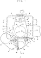
- Figs. 1- 6 show a SCARA arm 4 according to the embodiment.
- the SCARA arm 4 has a hand 2 (supporting member) for positioning and supporting articles and has arms 32, 34 for transferring articles with the advancement and retraction thereof from and to the counterparts of transfer such as cell supports 80, 81.
- Figs. 7 , 8 show the cell supports 80, 81 to and from which the SCARA arm transfers articles.
- Two species of articles comprising a FOUP 52 for 450mm wafers (the first article) and a FOUP 64 for 300mm wafers (the second article) are dealt with; however, any kind of articles may be dealt with.
- the second article is smaller than the first article in size and lower than the first article in height.
- chained lines show the FOUPs 52, 64, and their portions irrelevant to the invention, such as side flanges of the FOUPs 52, 64, are omitted.
- Figs. 1 , 4 , 7 , and 8 show the bottom structures of the FOUPs 52, 64 that are positioned by the hand 2 and the cell supports 80, 81.
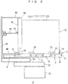
- Figs. 1 , 2 show the SCARA arm 4 which supports the FOUP 52 for 450mm wafers.
- the hand 2 is provided with a plate 6 that has thick portions 8, 9 at both the tip end and the base end, along the front and rear direction of the plate, and a thin portion 10 between them.
- the thick portion at the base end 9 is attached to a shaft 40 which rotates the hand 2.
- an end of the hand 2 near from the shaft 40 is referred to as the base end, the opposite thick portions 8 as the tip end, and the direction connecting the base and tip ends as the front and rear direction.
- An orthogonal direction to the front and rear direction in a horizontal plane is referred to as a lateral direction.
- the width of the plate 6 along the lateral direction is narrower than those of FOUPs 52, 64 so that the cell supports 80, 81 may support the FOUPs 52, 64.
- the thick portion 8 at the base end has a positioning guide 12 at the center portion of the thick portion along the lateral direction, and the thick portion 9 at the tip end has, for example, a pair of left and right positioning guides 16, 16.
- the positioning guides 12, 16 have the same structure except for their lengths and are provided with tapered surfaces 13, 17 which are inclined to be lower at the thin portion 10 and horizontal supporting surfaces 14, 18 which extend from the lower end of the tapered surfaces 13, 17 towards the thin portion 10.
- the thick portion 8 has, for example in plan view, a rectangular positioning protrusion 20 at a position near from the thin portion 10 and at the center portion of the thick portion along the lateral direction, and the positioning protrusion has R-shaped portions at the lateral edges.
- the thin portion 10 is provided with, for example, three kinematic coupling pins 22 (hereinafter referred to as pins 22), and the height of the pins 22 is lower than that of the supporting surfaces 14, 18.
- the upper surface of the thin portion 10 is made lower than the upper surface of the thick portion 8 by D, and therefore, there are difference in thickness D between the thick portions 8, 9 and the thin portion 10. Further, since the upper surface of the thin portion 10 is made lower than the upper surface of the thick portion 8, the height of the positioning guides 12, 16 can be made low.
- the SCARA arm 4 is provided with an arm 32 which rotates around an shaft 36 attached to a base 30 and also an arm 34 which rotates around a shaft 38 attached to a tip end of the arm 32, and said shaft 40 is provided at a tip end of the arm 34.
- the SCARA arm 4 is mounted on a carrier which is capable of rising and lowering and horizontal reciprocating.
- the carrier is provided in a stocker or the like for temporarily storing the FOUPs 52, 64, reciprocates along a rack, and supports, raises, and lowers the SCARA arm 4 by an arm 42.
- the combination of advancement and retraction of the SCARA arm 4 and rising and lowering of the base 30 performs the transfer of the FOUPs 52, 34 to and from the cell supports 80, 81.
- the anti-drop members 44, 46 are attached to a pillar 48 which stands vertically upright from the arm 34, and have respective fixed heights.
- the anti-drop member 44 is attached to a position near from the upward end of the pillar 44, and the anti-drop member 46 is attached to a lower position than the anti-drop member 44 is.
- the second anti-drop member 46 is attached to and rotatable, in a horizontal plane, around a shaft that is attached to the pillar 48 and has at the opposite tip end a roller 50 that rotates around a vertical axis.
- the first anti-drop member 44 prevents the FOUP 52 for 450mm wafers from dropping, and the second anti-drop member 46 prevents the FOUP 64 for 300mm wafers from dropping.
- the anti-drop member 44 regulates the upper end position of the door part 58 of the FOUP 52, and the anti-drop member 46 regulates the upper end position of the door part 68 of the FOUP 64. Further, the anti-drop member 46 retracts with the roller 50 being pushed by the end surface 59 of the door part 58, when in contact with the FOUP 52.
- the detailed structure of the anti-drop mechanism that comprises the anti-drop members 44, 46 and so on will be described later with reference to Fig. 6 .
- 69 designates the end surface of the door part 68 of the FOUP 64, and the end surface 59 is nearer to the pillar 48 than the end surface 69 is.
- the FOUP 52 for 450mm wafers is provided with the conveyor surfaces 54 on the four sides at the bottom.
- the side faces of the FOUP have, at their bottom ends, have conveyor guide surfaces 55 which intersect with the conveyor guide surfaces 54.
- the conveyor surfaces 54 and the conveyor guide surfaces 55 are flat and are provided at specified positions.
- the FOUP 52 is provided at the bottom with three V-grooves (inversely V-shaped grooves in section), and the V-grooves near from the door part 58 are referred to as V-grooves 56, and the V-groove far from the door part 58 is referred to as V-groove 57.
- the hand 2 positions the FOUP along the front and rear direction by the front and rear conveyor guide surfaces 55 and the positioning guides 12, 16 and supports the conveyor surfaces by the supporting surfaces 14, 18. Further, the positioning protrusion 20 positions the V-groove 57 which is opposite to the door part 58 so that the FOUP is positioned along the lateral direction. Since the positioning by the positioning protrusion 20 might allow the FOUP 52 to rotate about a vertical axis, the rotation of the FOUP 52 is inhibited by the anti-rotation elements 19.
- Figs. 1- 3 show how the FOUP 52 for 450mm wafers is supported.
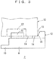
- one of the conveyor guide surfaces 55 is guided by the tapered surface 13 of the positioning guide 12, and one of the conveyor surfaces 54 is supported by the supporting surface 14.
- the tapered surfaces 17 guide one of the conveyor guide surfaces 55, and the supporting surfaces 18 support one of the conveyor surfaces 54.
- the FOUP 52 is positioned along the front and rear direction and is inhibited from rotation about a vertical axis by the anti-rotation elements 19.
- the FOUP 52 is positioned in a horizontal plane and has only one freedom of movement along the up and down direction.
- the first anti-drop member 44 regulates the height of the FOUP 52 so as to inhibit the falling and tumbling.
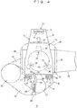
- Figs. 4 , 5 show the support of the FOUP 64 for 300mm wafers.
- the thin portion 10 has a length, along the front and rear direction, longer than the length or the depth of the FOUP 64, and the FOUP 64 is supported on the thin portion 10.
- the FOUP 64 is positioned, according to it's standard specification, with the kinematic coupling between the three V grooves 66 and the three pins 22, and the conveyor surfaces 65 are not used for the positioning. Since the FOUP 64 is smaller than the FOUP 52, and since the pins 22 are provided at positions corresponding to the V-grooves 66, the standard positioning becomes possible. Further, since the pins 22 are on the thin portion 10, they do not come in contact with the bottom of the FOUP 52.
- the positioning protrusion 20 is out of the bottom of the FOUP 64. Since the FOUP 64 is positioned by the pins 22 in a horizontal plane, the second anti-drop member 46 regulates the height of the FOUP 64 so as to inhibit the dropping and tumbling.
- the pillar 48 stands on the arm 34, and, when the arms 32, 34 advance from the state shown in Figs.1 , 4 , the anti-drop members 44, 46 do not come in contact with the top portions of FOUP 52, 64. Therefore, the anti-drop members 44, 46 do not interfere with the FOUPs 52, 64.
- the arms 32, 34 return to their positions of origin as shown in Figs. 1 , 4 , then the carrier becomes possible to travel. Further, when the arms 34 returns to the position of origin, the anti-drop members are moved to advance over the FOUPs 52, 64, the anti-drop member 44 advances over the door part 58 so as to prevent the FOUP 52 from dropping and tumbling.
- 60 designates elastic pieces which are provided on the bottoms of the anti-drop members 44, 46 and absorb the shock due to the contact with the FOUPs 52, 64. The elastic pieces 60 may be omitted.
- the anti-drop member 46 is rotatably supported around the vertical shaft 70 and is energized to advance over the FOUPs 52, 64 by an energizing member.
- 71, 72 designate brackets, 73 a bearing, and 74 a torsion spring, as an example of the energizing member. While the above elastic piece 60 is provided on the bottom of the tip end of the anti-drop member 46, it may be omitted.
- the orientation of the anti-drop member 46 is regulated by a stopper 76 so as to advance over the door part 68 of the FOUP 52.
- the roller 50 is supported by a bearing 78 so as to rotate about a vertical shaft 77. While the anti-drop member 46 retracts with the roller 50 being pushed by the front side of door part from the FOUP 52, the anti-drop member advances over the door part 68 of the FOUP 64 so as to prevent the dropping and the tumbling.
- the energizing member and the stopper 76 are provided so that the anti-drop member 46 advances and retracts according to the species of the FOUPs 52, 64, however a driving member, such as a solenoid or a motor, may be provided instead of them, in order to advance and retract the anti-drop member 46.
- a driving member such as a solenoid or a motor, may be provided instead of them, in order to advance and retract the anti-drop member 46.
- this configuration makes the anti-drop mechanism larger and increases the number of portions which need maintenance.
- Fig. 7 shows the support of the FOUP 52 for 450mm wafers by the cell supports 80, 81.
- Each of the cell supports 80,81 is provided with a positioning guide 82 for the front and rear direction, a positioning guide for the lateral direction, and a positioning guide 90 both for the front and rear direction and lateral direction and positions the FOUP 52 along the directions of front, rear, left, and right.
- 83 and 91 designate tapered surfaces inclined along the front and rear direction
- 87 and 92 designate tapered surfaces inclined along the lateral direction
- Fig. 8 shows the support of the FOUP 64 for 300mm wafers by the cell supports 80, 81.
- Positioning pins 94 associate with holes in the FOUP 64 for forklift trucks for positioning purpose. Further, the positioning pins 94 do not come into contact with the FOUP 52 for 450mm wafers, since they are accommodated in the V grooves 56.
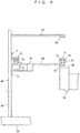
- Fig. 9 shows another anti-drop mechanism 100, according to a comparative example, for both the FOUPs 52 and 64.
- An adequate sensor is provided for discriminating the species of the FOUPs 52, 64, or a host controller informs the species of the FOUPs 62, 64.
- a direct motion mechanism comprising a ball screw 104 and a motor 106, elevates and lowers the anti-drop member 44, according to the species of the FOUP 52, 64.
- the comparative example needs more space for the direct motion mechanism, may generate particulates due to the direct motion mechanism, and has more portions which need maintenance.
- a SCARA arm 4 is used, however, the positioning guides 12, 16 and the positioning protrusion 20, and the pins 22 may be provided on the top plate of a slide fork, and the pillar 48 and the anti-drop member 44, 46 may be provided on the middle plate of the fork.
Landscapes
- Engineering & Computer Science (AREA)
- Mechanical Engineering (AREA)
- Container, Conveyance, Adherence, Positioning, Of Wafer (AREA)
- Warehouses Or Storage Devices (AREA)
Abstract

Description
- The invention relates to a supporting device for articles and a supporting method.
- Patent Document 1 (
JP4543567B JP4543567B - Patent Document 1:
JP4543567B - The object of the invention is to position plural species of articles which have different heights, to prevent them from dropping and tumbling, and to make the taller article in height not hinder to secure the lower article against dropping.
- A supporting device according to the invention supports a first article and a second article which is lower than the first article in height, and has a supporting member comprises:
- a first positioning member that positions a bottom of the first article and inhibits horizontal movement of the first article; and
- a second positioning member that positions a bottom of the second article and inhibits horizontal movement of the second article,
- wherein the first positioning member and the second positioning member are both configured to position the first article and the second article respectively when lowered on the supporting member and to release the first article and the second article respectively from positioning when elevated therefrom,
- the supporting device further comprises:
- a first anti-drop member that advances over the first article when the first article is positioned by the first positioning member and prevents the first article from elevating and thereby escaping from positioning; and
- a second anti-drop member that advances over the second article when the second article is positioned by the second positioning member and prevents the second article from elevating and thereby escaping from positioning,
- wherein said first positioning member is provided at a higher position than the second positioning member is,
- wherein said first anti-drop member and said second anti-drop member are provided at a same side of said supporting member in plan view,
- wherein said first positioning member and said second positioning member are configured to position one end of the first article that is on a side of said first anti-drop member and said second anti-drop member nearer or equally distant to said first anti-drop member and said second anti-drop member than one end of the second article that is on the side of said first anti-drop member and said second anti-drop member, and
- wherein said second anti-drop member is configured to retract from said one end of the first article, when said first positioning member positions the first article.
- A supporting method according to the invention supports a first article and a second article which is lower than the first article in height by a supporting device, comprises:
- positioning a bottom of the first article and inhibiting horizontal movement of the first article by a first positioning member of a supporting member of the supporting device and releasing the first article from positioning when the first article is elevated;
- positioning a bottom of the second article and inhibiting horizontal movement of the second article by a second positioning member of a supporting member of the supporting device and releasing the second article from positioning when the second article is elevated;
- advancing a first anti-drop member over the first article, when the first positioning member positions the first article, so as to prevent the first article from elevating and being released from positioning;
- advancing a second anti-drop member over the second article, when the second positioning member positions the second article, so as to prevent the second article from elevating and being released from positioning;
- wherein said first positioning member is provided at a higher position than the second positioning member is,
- wherein said first anti-drop member and said second anti-drop member are provided at a same side of said supporting member in plan view,
- wherein said first positioning member and said second positioning member position one end of the first article that is on a side of said first anti-drop member and said second anti-drop member nearer or equally distant to said first anti-drop member and said second anti-drop member than one end of the second article that is on the side of said first anti-drop member and said second anti-drop member, and
- retracting said second anti-drop member from said one end of the first article, when said first positioning member positions the first article. These steps may be carried out for example parallelly. In this specification, descriptions about the supporting device apply to the supporting method as they are.
- In the embodiment, the first and the second positioning members position and support the bottoms of the first and the second articles, however, the bottoms of the first and second articles may be supported by another supporting member. In plan view, the first anti-drop member and the second anti-drop member are on the same side of the supporting member. Further, the end of the first article on the side of the first and second anti-drop members is positioned at the same position to or at a nearer position than the nearest end of the second article from the first and second anti-drop members.
- Since the first article and the second article are released from the positioning, when they are lifted from the supporting member, they might drop or tumble. Therefore, the first anti-drop member and the second anti-drop member are made to occupy a higher space over these articles and prevent the articles from elevating and being released from the positioning. Since the end of the first article is positioned at the same position to or at a nearer position than the end of the second article from the first and the second anti-drop members, the second anti-drop member may interfere with the taller first article. Therefore, when the first positioning member positions the first article, said second anti-drop member is made to retract from said end of the first article.
- According to the invention, two species of articles which have different heights are positioned, the first anti-drop member prevents the first article from dropping and tumbling, and the second anti-drop member prevents the second article from dropping and tumbling. Further, since the second anti-drop member is retractable, the first article does not hinder the provision of the second anti-drop member. According to the invention, dropping and tumbling of articles are prevented, however, they may be simply referred to as prevention of dropping without reference to tumbling.
- Preferably, the second anti-drop member is configured to advance over the second article and to retract from the end of the first article when pushed by the first article, and an energizing member that energizes the second anti-drop member to advance over the second article is further provided. According to this configuration, the second anti-drop member advances over the second article without any driving mechanism and retracts when pushed by the first article. Therefore, a space for the driving mechanism is not needed, and the maintenance for the driving mechanism is also not needed.
- Further preferably, a moving member that advances said supporting member to an advanced position for transferring the first article and the second article between a counterpart of transfer and retracts said supporting member to a position of origin is provided; the first anti-drop member and the second anti-drop member are both provided at the moving member and configured so that, at the advanced position, the first anti-drop member and the second anti-drop member are both positionally separated from the first article and the second article and that, at the position of origin, the first anti-drop member advances over the first article and the second article, and that the second anti-drop member advances only over the second article. According to this configuration, the supporting device is integrated in a transfer apparatus for articles, and the first anti-drop member and the second anti-drop member move between positions over the articles and positions separated from the articles by the movements of the moving member. Further, the second anti-drop member advances and retracts with the energizement by the energizing member and the pushing force exerted by the first article, in addition to the movement of the moving member.
- Preferably, the first anti-drop member and the second anti-drop member are attached to a common pillar at a higher position and at a lower position respectively, and the second anti-drop member is rotatably attached around a vertical shaft to said pillar. Since the second anti-drop member rotates around the vertical shaft, a smaller space is needed for the advancement and retraction, in comparison with horizontal advancement and retraction.
- Further preferably, the second anti-drop member is provided with a roller that contacts the end of the first article. According to this configuration, the second anti-drop member contacts with the first article gently, and for example particle generation due to the contact is decreased.
- Particularly preferably, a stopper that restricts the range of rotation of the second anti-drop member is provided to halt the second anti-drop member at a position over the second article. According to this configuration, the second anti-drop member is energized by the energizing member, positioned by the stopper, and advances reliably over the second article.
-
- [
Fig. 1 ] A plan view wherein a SCARA arm that is equipped with a supporting device according to an embodiment supports a first article (FOUP for 450mm wafer) - [
Fig. 2 ] A side view wherein the SCARA arm supports the first article - [
Fig. 3 ] A partially enlarged side view ofFig. 2 indicating positioning of the first article by a positioning protrusion - [
Fig. 4 ] A plan view wherein the SCARA arm supports a second article (FOUP for 300mm wafer) - [
Fig. 5 ] A side view wherein the SCARA arm supports the second article - [
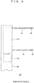
Fig. 6 ]A partially enlarged side view ofFig. 5 indicating an anti-drop mechanism - [
Fig. 7 ] A plan view of cell supports which support the first article - [
Fig. 8 ] A plan view of cell supports which support the second article - [
Fig. 9 ] A side view of an anti-drop mechanism according to a comparative example - The best embodiment for carrying out the invention will be described in the following. The scope of the invention shall be determined based upon the claims with reference to the specification and well-known arts in the field.
-
Figs. 1- 6 show aSCARA arm 4 according to the embodiment. TheSCARA arm 4 has a hand 2 (supporting member) for positioning and supporting articles and hasarms Figs. 7 ,8 show the cell supports 80, 81 to and from which the SCARA arm transfers articles. - Two species of articles comprising a
FOUP 52 for 450mm wafers (the first article) and aFOUP 64 for 300mm wafers (the second article) are dealt with; however, any kind of articles may be dealt with. The second article is smaller than the first article in size and lower than the first article in height. In the drawings, chained lines show theFOUPs FOUPs Figs. 1 ,4 ,7 , and8 show the bottom structures of theFOUPs hand 2 and the cell supports 80, 81. -
Figs. 1 ,2 show theSCARA arm 4 which supports theFOUP 52 for 450mm wafers. Thehand 2 is provided with aplate 6 that hasthick portions thin portion 10 between them. The thick portion at thebase end 9 is attached to ashaft 40 which rotates thehand 2. In the specification, an end of thehand 2 near from theshaft 40 is referred to as the base end, the oppositethick portions 8 as the tip end, and the direction connecting the base and tip ends as the front and rear direction. An orthogonal direction to the front and rear direction in a horizontal plane is referred to as a lateral direction. - The width of the
plate 6 along the lateral direction is narrower than those ofFOUPs FOUPs thick portion 8 at the base end has apositioning guide 12 at the center portion of the thick portion along the lateral direction, and thethick portion 9 at the tip end has, for example, a pair of left and right positioning guides 16, 16. The positioning guides 12, 16 have the same structure except for their lengths and are provided with taperedsurfaces thin portion 10 and horizontal supportingsurfaces thin portion 10. The outer-most points 19 of the positioning guides 12, 16 along the lateral direction, at the boundary between thetapered surfaces surfaces FOUP 52. - The
thick portion 8 has, for example in plan view, arectangular positioning protrusion 20 at a position near from thethin portion 10 and at the center portion of the thick portion along the lateral direction, and the positioning protrusion has R-shaped portions at the lateral edges. Thethin portion 10 is provided with, for example, three kinematic coupling pins 22 (hereinafter referred to as pins 22), and the height of thepins 22 is lower than that of the supportingsurfaces thin portion 10 is made lower than the upper surface of thethick portion 8 by D, and therefore, there are difference in thickness D between thethick portions thin portion 10. Further, since the upper surface of thethin portion 10 is made lower than the upper surface of thethick portion 8, the height of the positioning guides 12, 16 can be made low. - The
SCARA arm 4 is provided with anarm 32 which rotates around anshaft 36 attached to abase 30 and also anarm 34 which rotates around ashaft 38 attached to a tip end of thearm 32, and saidshaft 40 is provided at a tip end of thearm 34. TheSCARA arm 4 is mounted on a carrier which is capable of rising and lowering and horizontal reciprocating. The carrier is provided in a stocker or the like for temporarily storing theFOUPs SCARA arm 4 by anarm 42. The combination of advancement and retraction of theSCARA arm 4 and rising and lowering of thebase 30 performs the transfer of theFOUPs - 44 designates a first anti-drop member, and 46 a second anti-drop member. The
anti-drop members pillar 48 which stands vertically upright from thearm 34, and have respective fixed heights. Theanti-drop member 44 is attached to a position near from the upward end of thepillar 44, and theanti-drop member 46 is attached to a lower position than theanti-drop member 44 is. The secondanti-drop member 46 is attached to and rotatable, in a horizontal plane, around a shaft that is attached to thepillar 48 and has at the opposite tip end aroller 50 that rotates around a vertical axis. The firstanti-drop member 44 prevents theFOUP 52 for 450mm wafers from dropping, and the secondanti-drop member 46 prevents theFOUP 64 for 300mm wafers from dropping. Theanti-drop member 44 regulates the upper end position of thedoor part 58 of theFOUP 52, and theanti-drop member 46 regulates the upper end position of thedoor part 68 of theFOUP 64. Further, theanti-drop member 46 retracts with theroller 50 being pushed by theend surface 59 of thedoor part 58, when in contact with theFOUP 52. The detailed structure of the anti-drop mechanism that comprises theanti-drop members Fig. 6 . Further, 69 designates the end surface of thedoor part 68 of theFOUP 64, and theend surface 59 is nearer to thepillar 48 than theend surface 69 is. - As shown in
Figs.1 ,2 , theFOUP 52 for 450mm wafers is provided with the conveyor surfaces 54 on the four sides at the bottom. The side faces of the FOUP have, at their bottom ends, have conveyor guide surfaces 55 which intersect with the conveyor guide surfaces 54. The conveyor surfaces 54 and the conveyor guide surfaces 55 are flat and are provided at specified positions. TheFOUP 52 is provided at the bottom with three V-grooves (inversely V-shaped grooves in section), and the V-grooves near from thedoor part 58 are referred to as V-grooves 56, and the V-groove far from thedoor part 58 is referred to as V-groove 57. Thehand 2 positions the FOUP along the front and rear direction by the front and rear conveyor guide surfaces 55 and the positioning guides 12, 16 and supports the conveyor surfaces by the supportingsurfaces positioning protrusion 20 positions the V-groove 57 which is opposite to thedoor part 58 so that the FOUP is positioned along the lateral direction. Since the positioning by thepositioning protrusion 20 might allow theFOUP 52 to rotate about a vertical axis, the rotation of theFOUP 52 is inhibited by theanti-rotation elements 19. -
Figs. 1- 3 show how theFOUP 52 for 450mm wafers is supported. As shown inFig. 3 , one of the conveyor guide surfaces 55 is guided by the taperedsurface 13 of thepositioning guide 12, and one of the conveyor surfaces 54 is supported by the supportingsurface 14. Similarly, on the positioning guides 16, thetapered surfaces 17 guide one of the conveyor guide surfaces 55, and the supportingsurfaces 18 support one of the conveyor surfaces 54. Thereby, theFOUP 52 is positioned along the front and rear direction and is inhibited from rotation about a vertical axis by theanti-rotation elements 19. Thus, theFOUP 52 is positioned in a horizontal plane and has only one freedom of movement along the up and down direction. When large acceleration is exerted to theFOUP 52 with the movement of theSCARA arm 4 or the carrier which is provided with theSCARA arm 4, theFOUP 52 might fall or tumble. Therefore, the firstanti-drop member 44 regulates the height of theFOUP 52 so as to inhibit the falling and tumbling. -
Figs. 4 ,5 show the support of theFOUP 64 for 300mm wafers. Thethin portion 10 has a length, along the front and rear direction, longer than the length or the depth of theFOUP 64, and theFOUP 64 is supported on thethin portion 10. TheFOUP 64 is positioned, according to it's standard specification, with the kinematic coupling between the threeV grooves 66 and the threepins 22, and the conveyor surfaces 65 are not used for the positioning. Since theFOUP 64 is smaller than theFOUP 52, and since thepins 22 are provided at positions corresponding to the V-grooves 66, the standard positioning becomes possible. Further, since thepins 22 are on thethin portion 10, they do not come in contact with the bottom of theFOUP 52. Moreover, thepositioning protrusion 20 is out of the bottom of theFOUP 64. Since theFOUP 64 is positioned by thepins 22 in a horizontal plane, the secondanti-drop member 46 regulates the height of theFOUP 64 so as to inhibit the dropping and tumbling. - As shown in
Fig. 6 , thepillar 48 stands on thearm 34, and, when thearms Figs.1 ,4 , theanti-drop members FOUP anti-drop members FOUPs arms Figs. 1 ,4 , then the carrier becomes possible to travel. Further, when thearms 34 returns to the position of origin, the anti-drop members are moved to advance over theFOUPs anti-drop member 44 advances over thedoor part 58 so as to prevent theFOUP 52 from dropping and tumbling. By the way, 60 designates elastic pieces which are provided on the bottoms of theanti-drop members FOUPs elastic pieces 60 may be omitted. - The
anti-drop member 46 is rotatably supported around thevertical shaft 70 and is energized to advance over theFOUPs elastic piece 60 is provided on the bottom of the tip end of theanti-drop member 46, it may be omitted. The orientation of theanti-drop member 46 is regulated by astopper 76 so as to advance over thedoor part 68 of theFOUP 52. Theroller 50 is supported by a bearing 78 so as to rotate about avertical shaft 77. While theanti-drop member 46 retracts with theroller 50 being pushed by the front side of door part from theFOUP 52, the anti-drop member advances over thedoor part 68 of theFOUP 64 so as to prevent the dropping and the tumbling. - In the embodiment, the energizing member and the
stopper 76 are provided so that theanti-drop member 46 advances and retracts according to the species of theFOUPs anti-drop member 46. However, this configuration makes the anti-drop mechanism larger and increases the number of portions which need maintenance. -
Fig. 7 shows the support of theFOUP 52 for 450mm wafers by the cell supports 80, 81. Each of the cell supports 80,81 is provided with apositioning guide 82 for the front and rear direction, a positioning guide for the lateral direction, and apositioning guide 90 both for the front and rear direction and lateral direction and positions theFOUP 52 along the directions of front, rear, left, and right. 83 and 91 designate tapered surfaces inclined along the front and rear direction, 87 and 92 designate tapered surfaces inclined along the lateral direction, and the tapered surfaces guide the conveyor surfaces 54. -
Fig. 8 shows the support of theFOUP 64 for 300mm wafers by the cell supports 80, 81. Positioning pins 94 associate with holes in theFOUP 64 for forklift trucks for positioning purpose. Further, the positioning pins 94 do not come into contact with theFOUP 52 for 450mm wafers, since they are accommodated in theV grooves 56. -
Fig. 9 shows anotheranti-drop mechanism 100, according to a comparative example, for both the FOUPs 52 and 64. An adequate sensor is provided for discriminating the species of theFOUPs FOUPs 62, 64. Along avertical pillar 102 standing from thearm 34, a direct motion mechanism, comprising a ball screw 104 and amotor 106, elevates and lowers theanti-drop member 44, according to the species of theFOUP - In the embodiment, a
SCARA arm 4 is used, however, the positioning guides 12, 16 and thepositioning protrusion 20, and thepins 22 may be provided on the top plate of a slide fork, and thepillar 48 and theanti-drop member Description of Symbols 2 hand (supporting member) 4 SCARA arm (supporting device for an article) 6 plate 8,9 thick portion 10 thin portion 12,16 positioning guide (first positioning member) 13,17 tapered surface 14,18 supporting surface 19 anti-rotation element 20 positioning protrusion (first positioning member) 22 kinematic coupling pin (second positioning member) 30 base 32,34 arm 36-40 shaft 42 arm 44 first anti-drop member 46 second anti-drop member 48 pillar 50 roller 52 FOUP for 450mm wafers (first article) 54 conveyor surface 55 conveyor guide surface 56 V- groove 58 door part 59,69 end surface 64 FOUP for 300mm wafers (second article) 65 conveyor surface 66 V- groove 68 door part 70 shaft 71,72 bracket 73,78 bearing 74 torsion spring (energizing member) 75 elastic piece 76 stopper 77 shaft 80,81 cell support 82,86,90 positioning guide 83,87,91,92 tapered surface 84,88,93 supporting surface 94 positioning pin 100 anti-drop mechanism 102 pillar 104 ball screw 103 motor D difference in thickness
Claims (7)
- A supporting device for supporting a first article and a second article which is lower than the first article in height, comprising:a supporting member including a first positioning member that positions a bottom of the first article and inhibits horizontal movement of the first article; and a second positioning member that positions a bottom of the second article and inhibits horizontal movement of the second article;wherein the first positioning member and the second positioning member are both configured to position the first article and the second article respectively when lowered on the supporting member and to release the first article and the second article respectively from positioning when elevated therefrom,the supporting device further comprising:a first anti-drop member that advances over the first article when the first article is positioned by the first positioning member and prevents the first article from elevating and thereby escaping from positioning; anda second anti-drop member that advances over the second article when the second article is positioned by the second positioning member and prevents the second article from elevating and thereby escaping from positioning,wherein said first positioning member is provided at a higher position than the second positioning member is,wherein said first anti-drop member and said second anti-drop member are provided at a same side of said supporting member in plan view,wherein said first positioning member and said second positioning member are configured to position one end of the first article that is on a side of said first anti-drop member and said second anti-drop member nearer or equally distant to said first anti-drop member and said second anti-drop member than one end of the second article that is on the side of said first anti-drop member and said second anti-drop member, andwherein said second anti-drop member is configured to retract from said one end of the first article, when said first positioning member positions the first article.
- A supporting device according to claim 1, wherein the second anti-drop member is configured to advance over the second article and to retract from said one end of the first article when pushed by the first article,
the supporting device further comprising an energizing member that energizes the second anti-drop member to advance over the second article. - A supporting device according to claim 2, further comprising a moving member that advances said supporting member to an advanced position for transferring the first article and the second article between a counterpart of transfer and retracts said supporting member to a position of origin,
wherein the first anti-drop member and the second anti-drop member are both provided at the moving member and configured so thatat the advanced position, the first anti-drop member and the second anti-drop member are both positionally separated from the first article and the second article and thatat the position of origin, the first anti-drop member advances over the first article and the second article, and that the second anti-drop member advances only over the second article. - A supporting device according to one of claims 1- 3, wherein the first anti-drop member and the second anti-drop member are attached to a common pillar at a higher position and at a lower position respectively,
wherein the second anti-drop member is rotatably attached around a vertical shaft to said pillar. - A supporting device according to claim 4, wherein the second anti-drop member is provided with a roller that contact said one end of the first article.
- A supporting device according to claim 5, further comprising a stopper that restricts range of rotation of the second anti-drop member to halt the second anti-drop member at a position over the second article.
- A supporting method by a supporting device for supporting a first article and a second article which is lower than the first article in height, comprising:positioning a bottom of the first article and inhibiting horizontal movement of the first article by a first positioning member of a supporting member of the supporting device and releasing the first article from positioning when the first article is elevated;positioning a bottom of the second article and inhibiting horizontal movement of the second article by a second positioning member of a supporting member of the supporting device and releasing the second article from positioning when the second article is elevated;advancing a first anti-drop member over the first article, when the first positioning member positions the first article, so as to prevent the first article from elevating and being released from positioning;advancing a second anti-drop member over the second article, when the second positioning member positions the second article, so as to prevent the second article from elevating and being released from positioning;wherein said first positioning member is provided at a higher position than the second positioning member is,wherein said first anti-drop member and said second anti-drop member are provided on a same side of said supporting member in plan view,wherein said first positioning member and said second positioning member position one end of the first article that is on a side of said first anti-drop member and said second anti-drop member nearer or equally distant to said first anti-drop member and said second anti-drop member than one end of the second article that is on the side of said first anti-drop member and said second anti-drop member, andretracting said second anti-drop member from said one end of the first article, when said first positioning member positions the first article.
Applications Claiming Priority (2)
| Application Number | Priority Date | Filing Date | Title |
|---|---|---|---|
| JP2015063643 | 2015-03-26 | ||
| PCT/JP2016/053490 WO2016152276A1 (en) | 2015-03-26 | 2016-02-05 | Supporting device and supporting method for articles |
Publications (3)
| Publication Number | Publication Date |
|---|---|
| EP3275809A1 true EP3275809A1 (en) | 2018-01-31 |
| EP3275809A4 EP3275809A4 (en) | 2018-11-21 |
| EP3275809B1 EP3275809B1 (en) | 2019-10-23 |
Family
ID=56977972
Family Applications (1)
| Application Number | Title | Priority Date | Filing Date |
|---|---|---|---|
| EP16768179.0A Active EP3275809B1 (en) | 2015-03-26 | 2016-02-05 | Supporting device and supporting method for articles |
Country Status (9)
| Country | Link |
|---|---|
| US (1) | US10475684B2 (en) |
| EP (1) | EP3275809B1 (en) |
| JP (1) | JP6410068B2 (en) |
| KR (1) | KR101967272B1 (en) |
| CN (1) | CN107406195B (en) |
| IL (1) | IL253640B (en) |
| SG (1) | SG11201706227SA (en) |
| TW (1) | TWI661986B (en) |
| WO (1) | WO2016152276A1 (en) |
Families Citing this family (319)
| Publication number | Priority date | Publication date | Assignee | Title |
|---|---|---|---|---|
| US9394608B2 (en) | 2009-04-06 | 2016-07-19 | Asm America, Inc. | Semiconductor processing reactor and components thereof |
| US8802201B2 (en) | 2009-08-14 | 2014-08-12 | Asm America, Inc. | Systems and methods for thin-film deposition of metal oxides using excited nitrogen-oxygen species |
| US20130023129A1 (en) | 2011-07-20 | 2013-01-24 | Asm America, Inc. | Pressure transmitter for a semiconductor processing environment |
| US9017481B1 (en) | 2011-10-28 | 2015-04-28 | Asm America, Inc. | Process feed management for semiconductor substrate processing |
| US10714315B2 (en) | 2012-10-12 | 2020-07-14 | Asm Ip Holdings B.V. | Semiconductor reaction chamber showerhead |
| US20160376700A1 (en) | 2013-02-01 | 2016-12-29 | Asm Ip Holding B.V. | System for treatment of deposition reactor |
| US11015245B2 (en) | 2014-03-19 | 2021-05-25 | Asm Ip Holding B.V. | Gas-phase reactor and system having exhaust plenum and components thereof |
| US10858737B2 (en) | 2014-07-28 | 2020-12-08 | Asm Ip Holding B.V. | Showerhead assembly and components thereof |
| US9890456B2 (en) | 2014-08-21 | 2018-02-13 | Asm Ip Holding B.V. | Method and system for in situ formation of gas-phase compounds |
| US10941490B2 (en) | 2014-10-07 | 2021-03-09 | Asm Ip Holding B.V. | Multiple temperature range susceptor, assembly, reactor and system including the susceptor, and methods of using the same |
| US10276355B2 (en) | 2015-03-12 | 2019-04-30 | Asm Ip Holding B.V. | Multi-zone reactor, system including the reactor, and method of using the same |
| JP6332133B2 (en) * | 2015-05-14 | 2018-05-30 | 株式会社ダイフク | Container transfer equipment |
| US10458018B2 (en) | 2015-06-26 | 2019-10-29 | Asm Ip Holding B.V. | Structures including metal carbide material, devices including the structures, and methods of forming same |
| JP6460245B2 (en) * | 2015-08-27 | 2019-01-30 | 村田機械株式会社 | Extraction device and storage device |
| US10211308B2 (en) | 2015-10-21 | 2019-02-19 | Asm Ip Holding B.V. | NbMC layers |
| US11139308B2 (en) | 2015-12-29 | 2021-10-05 | Asm Ip Holding B.V. | Atomic layer deposition of III-V compounds to form V-NAND devices |
| US10529554B2 (en) | 2016-02-19 | 2020-01-07 | Asm Ip Holding B.V. | Method for forming silicon nitride film selectively on sidewalls or flat surfaces of trenches |
| US10343920B2 (en) | 2016-03-18 | 2019-07-09 | Asm Ip Holding B.V. | Aligned carbon nanotubes |
| US10190213B2 (en) | 2016-04-21 | 2019-01-29 | Asm Ip Holding B.V. | Deposition of metal borides |
| US10865475B2 (en) | 2016-04-21 | 2020-12-15 | Asm Ip Holding B.V. | Deposition of metal borides and silicides |
| US10367080B2 (en) | 2016-05-02 | 2019-07-30 | Asm Ip Holding B.V. | Method of forming a germanium oxynitride film |
| US11453943B2 (en) | 2016-05-25 | 2022-09-27 | Asm Ip Holding B.V. | Method for forming carbon-containing silicon/metal oxide or nitride film by ALD using silicon precursor and hydrocarbon precursor |
| US9859151B1 (en) | 2016-07-08 | 2018-01-02 | Asm Ip Holding B.V. | Selective film deposition method to form air gaps |
| US10612137B2 (en) | 2016-07-08 | 2020-04-07 | Asm Ip Holdings B.V. | Organic reactants for atomic layer deposition |
| US10714385B2 (en) | 2016-07-19 | 2020-07-14 | Asm Ip Holding B.V. | Selective deposition of tungsten |
| JP6593270B2 (en) * | 2016-07-26 | 2019-10-23 | 株式会社ダイフク | Goods transport equipment |
| KR102532607B1 (en) | 2016-07-28 | 2023-05-15 | 에이에스엠 아이피 홀딩 비.브이. | Substrate processing apparatus and method of operating the same |
| US9887082B1 (en) | 2016-07-28 | 2018-02-06 | Asm Ip Holding B.V. | Method and apparatus for filling a gap |
| US9812320B1 (en) | 2016-07-28 | 2017-11-07 | Asm Ip Holding B.V. | Method and apparatus for filling a gap |
| US10643826B2 (en) | 2016-10-26 | 2020-05-05 | Asm Ip Holdings B.V. | Methods for thermally calibrating reaction chambers |
| US11532757B2 (en) | 2016-10-27 | 2022-12-20 | Asm Ip Holding B.V. | Deposition of charge trapping layers |
| US10714350B2 (en) | 2016-11-01 | 2020-07-14 | ASM IP Holdings, B.V. | Methods for forming a transition metal niobium nitride film on a substrate by atomic layer deposition and related semiconductor device structures |
| US10229833B2 (en) | 2016-11-01 | 2019-03-12 | Asm Ip Holding B.V. | Methods for forming a transition metal nitride film on a substrate by atomic layer deposition and related semiconductor device structures |
| KR102546317B1 (en) | 2016-11-15 | 2023-06-21 | 에이에스엠 아이피 홀딩 비.브이. | Gas supply unit and substrate processing apparatus including the same |
| KR102762543B1 (en) | 2016-12-14 | 2025-02-05 | 에이에스엠 아이피 홀딩 비.브이. | Substrate processing apparatus |
| US11581186B2 (en) | 2016-12-15 | 2023-02-14 | Asm Ip Holding B.V. | Sequential infiltration synthesis apparatus |
| US11447861B2 (en) | 2016-12-15 | 2022-09-20 | Asm Ip Holding B.V. | Sequential infiltration synthesis apparatus and a method of forming a patterned structure |
| KR102700194B1 (en) | 2016-12-19 | 2024-08-28 | 에이에스엠 아이피 홀딩 비.브이. | Substrate processing apparatus |
| US10269558B2 (en) | 2016-12-22 | 2019-04-23 | Asm Ip Holding B.V. | Method of forming a structure on a substrate |
| US10867788B2 (en) | 2016-12-28 | 2020-12-15 | Asm Ip Holding B.V. | Method of forming a structure on a substrate |
| US11390950B2 (en) | 2017-01-10 | 2022-07-19 | Asm Ip Holding B.V. | Reactor system and method to reduce residue buildup during a film deposition process |
| US10468261B2 (en) | 2017-02-15 | 2019-11-05 | Asm Ip Holding B.V. | Methods for forming a metallic film on a substrate by cyclical deposition and related semiconductor device structures |
| US10529563B2 (en) | 2017-03-29 | 2020-01-07 | Asm Ip Holdings B.V. | Method for forming doped metal oxide films on a substrate by cyclical deposition and related semiconductor device structures |
| KR102457289B1 (en) | 2017-04-25 | 2022-10-21 | 에이에스엠 아이피 홀딩 비.브이. | Method for depositing a thin film and manufacturing a semiconductor device |
| US10892156B2 (en) | 2017-05-08 | 2021-01-12 | Asm Ip Holding B.V. | Methods for forming a silicon nitride film on a substrate and related semiconductor device structures |
| US10770286B2 (en) | 2017-05-08 | 2020-09-08 | Asm Ip Holdings B.V. | Methods for selectively forming a silicon nitride film on a substrate and related semiconductor device structures |
| US10532884B2 (en) * | 2017-05-24 | 2020-01-14 | Hall Labs Llc | Mechanical end effector for planar motion mechanism |
| US10886123B2 (en) | 2017-06-02 | 2021-01-05 | Asm Ip Holding B.V. | Methods for forming low temperature semiconductor layers and related semiconductor device structures |
| US12040200B2 (en) | 2017-06-20 | 2024-07-16 | Asm Ip Holding B.V. | Semiconductor processing apparatus and methods for calibrating a semiconductor processing apparatus |
| US11306395B2 (en) | 2017-06-28 | 2022-04-19 | Asm Ip Holding B.V. | Methods for depositing a transition metal nitride film on a substrate by atomic layer deposition and related deposition apparatus |
| US10685834B2 (en) | 2017-07-05 | 2020-06-16 | Asm Ip Holdings B.V. | Methods for forming a silicon germanium tin layer and related semiconductor device structures |
| KR20190009245A (en) | 2017-07-18 | 2019-01-28 | 에이에스엠 아이피 홀딩 비.브이. | Methods for forming a semiconductor device structure and related semiconductor device structures |
| US11018002B2 (en) | 2017-07-19 | 2021-05-25 | Asm Ip Holding B.V. | Method for selectively depositing a Group IV semiconductor and related semiconductor device structures |
| US11374112B2 (en) | 2017-07-19 | 2022-06-28 | Asm Ip Holding B.V. | Method for depositing a group IV semiconductor and related semiconductor device structures |
| US10541333B2 (en) | 2017-07-19 | 2020-01-21 | Asm Ip Holding B.V. | Method for depositing a group IV semiconductor and related semiconductor device structures |
| US10590535B2 (en) | 2017-07-26 | 2020-03-17 | Asm Ip Holdings B.V. | Chemical treatment, deposition and/or infiltration apparatus and method for using the same |
| TWI815813B (en) | 2017-08-04 | 2023-09-21 | 荷蘭商Asm智慧財產控股公司 | Showerhead assembly for distributing a gas within a reaction chamber |
| US10770336B2 (en) | 2017-08-08 | 2020-09-08 | Asm Ip Holding B.V. | Substrate lift mechanism and reactor including same |
| US10692741B2 (en) | 2017-08-08 | 2020-06-23 | Asm Ip Holdings B.V. | Radiation shield |
| US11769682B2 (en) | 2017-08-09 | 2023-09-26 | Asm Ip Holding B.V. | Storage apparatus for storing cassettes for substrates and processing apparatus equipped therewith |
| US11139191B2 (en) | 2017-08-09 | 2021-10-05 | Asm Ip Holding B.V. | Storage apparatus for storing cassettes for substrates and processing apparatus equipped therewith |
| US11830730B2 (en) | 2017-08-29 | 2023-11-28 | Asm Ip Holding B.V. | Layer forming method and apparatus |
| KR102491945B1 (en) | 2017-08-30 | 2023-01-26 | 에이에스엠 아이피 홀딩 비.브이. | Substrate processing apparatus |
| US11056344B2 (en) | 2017-08-30 | 2021-07-06 | Asm Ip Holding B.V. | Layer forming method |
| US11295980B2 (en) | 2017-08-30 | 2022-04-05 | Asm Ip Holding B.V. | Methods for depositing a molybdenum metal film over a dielectric surface of a substrate by a cyclical deposition process and related semiconductor device structures |
| KR102401446B1 (en) | 2017-08-31 | 2022-05-24 | 에이에스엠 아이피 홀딩 비.브이. | Substrate processing apparatus |
| KR102630301B1 (en) | 2017-09-21 | 2024-01-29 | 에이에스엠 아이피 홀딩 비.브이. | Method of sequential infiltration synthesis treatment of infiltrateable material and structures and devices formed using same |
| US10844484B2 (en) | 2017-09-22 | 2020-11-24 | Asm Ip Holding B.V. | Apparatus for dispensing a vapor phase reactant to a reaction chamber and related methods |
| US10658205B2 (en) | 2017-09-28 | 2020-05-19 | Asm Ip Holdings B.V. | Chemical dispensing apparatus and methods for dispensing a chemical to a reaction chamber |
| US10403504B2 (en) | 2017-10-05 | 2019-09-03 | Asm Ip Holding B.V. | Method for selectively depositing a metallic film on a substrate |
| US10319588B2 (en) | 2017-10-10 | 2019-06-11 | Asm Ip Holding B.V. | Method for depositing a metal chalcogenide on a substrate by cyclical deposition |
| US10923344B2 (en) | 2017-10-30 | 2021-02-16 | Asm Ip Holding B.V. | Methods for forming a semiconductor structure and related semiconductor structures |
| US10910262B2 (en) | 2017-11-16 | 2021-02-02 | Asm Ip Holding B.V. | Method of selectively depositing a capping layer structure on a semiconductor device structure |
| US11022879B2 (en) | 2017-11-24 | 2021-06-01 | Asm Ip Holding B.V. | Method of forming an enhanced unexposed photoresist layer |
| CN111316417B (en) | 2017-11-27 | 2023-12-22 | 阿斯莫Ip控股公司 | Storage device for use with batch furnaces for storing wafer cassettes |
| JP7206265B2 (en) | 2017-11-27 | 2023-01-17 | エーエスエム アイピー ホールディング ビー.ブイ. | Equipment with a clean mini-environment |
| JP6801640B2 (en) * | 2017-12-21 | 2020-12-16 | 株式会社ダイフク | Storage shelves and goods storage equipment |
| US10872771B2 (en) | 2018-01-16 | 2020-12-22 | Asm Ip Holding B. V. | Method for depositing a material film on a substrate within a reaction chamber by a cyclical deposition process and related device structures |
| TWI799494B (en) | 2018-01-19 | 2023-04-21 | 荷蘭商Asm 智慧財產控股公司 | Deposition method |
| CN111630203A (en) | 2018-01-19 | 2020-09-04 | Asm Ip私人控股有限公司 | Method of depositing a gap fill layer by plasma assisted deposition |
| US11018047B2 (en) | 2018-01-25 | 2021-05-25 | Asm Ip Holding B.V. | Hybrid lift pin |
| USD880437S1 (en) | 2018-02-01 | 2020-04-07 | Asm Ip Holding B.V. | Gas supply plate for semiconductor manufacturing apparatus |
| US11081345B2 (en) | 2018-02-06 | 2021-08-03 | Asm Ip Holding B.V. | Method of post-deposition treatment for silicon oxide film |
| US10896820B2 (en) | 2018-02-14 | 2021-01-19 | Asm Ip Holding B.V. | Method for depositing a ruthenium-containing film on a substrate by a cyclical deposition process |
| JP7124098B2 (en) | 2018-02-14 | 2022-08-23 | エーエスエム・アイピー・ホールディング・ベー・フェー | Method for depositing a ruthenium-containing film on a substrate by a cyclical deposition process |
| US10731249B2 (en) | 2018-02-15 | 2020-08-04 | Asm Ip Holding B.V. | Method of forming a transition metal containing film on a substrate by a cyclical deposition process, a method for supplying a transition metal halide compound to a reaction chamber, and related vapor deposition apparatus |
| KR102636427B1 (en) | 2018-02-20 | 2024-02-13 | 에이에스엠 아이피 홀딩 비.브이. | Substrate processing method and apparatus |
| US10975470B2 (en) | 2018-02-23 | 2021-04-13 | Asm Ip Holding B.V. | Apparatus for detecting or monitoring for a chemical precursor in a high temperature environment |
| US11473195B2 (en) | 2018-03-01 | 2022-10-18 | Asm Ip Holding B.V. | Semiconductor processing apparatus and a method for processing a substrate |
| US11629406B2 (en) | 2018-03-09 | 2023-04-18 | Asm Ip Holding B.V. | Semiconductor processing apparatus comprising one or more pyrometers for measuring a temperature of a substrate during transfer of the substrate |
| US11114283B2 (en) | 2018-03-16 | 2021-09-07 | Asm Ip Holding B.V. | Reactor, system including the reactor, and methods of manufacturing and using same |
| KR102646467B1 (en) | 2018-03-27 | 2024-03-11 | 에이에스엠 아이피 홀딩 비.브이. | Method of forming an electrode on a substrate and a semiconductor device structure including an electrode |
| US11230766B2 (en) | 2018-03-29 | 2022-01-25 | Asm Ip Holding B.V. | Substrate processing apparatus and method |
| US11088002B2 (en) | 2018-03-29 | 2021-08-10 | Asm Ip Holding B.V. | Substrate rack and a substrate processing system and method |
| KR102501472B1 (en) | 2018-03-30 | 2023-02-20 | 에이에스엠 아이피 홀딩 비.브이. | Substrate processing method |
| KR102600229B1 (en) | 2018-04-09 | 2023-11-10 | 에이에스엠 아이피 홀딩 비.브이. | Substrate supporting device, substrate processing apparatus including the same and substrate processing method |
| KR102709511B1 (en) | 2018-05-08 | 2024-09-24 | 에이에스엠 아이피 홀딩 비.브이. | Methods for depositing an oxide film on a substrate by a cyclical deposition process and related device structures |
| US12025484B2 (en) | 2018-05-08 | 2024-07-02 | Asm Ip Holding B.V. | Thin film forming method |
| US12272527B2 (en) | 2018-05-09 | 2025-04-08 | Asm Ip Holding B.V. | Apparatus for use with hydrogen radicals and method of using same |
| TWI816783B (en) | 2018-05-11 | 2023-10-01 | 荷蘭商Asm 智慧財產控股公司 | Methods for forming a doped metal carbide film on a substrate and related semiconductor device structures |
| KR102596988B1 (en) | 2018-05-28 | 2023-10-31 | 에이에스엠 아이피 홀딩 비.브이. | Method of processing a substrate and a device manufactured by the same |
| TWI840362B (en) | 2018-06-04 | 2024-05-01 | 荷蘭商Asm Ip私人控股有限公司 | Wafer handling chamber with moisture reduction |
| US11718913B2 (en) | 2018-06-04 | 2023-08-08 | Asm Ip Holding B.V. | Gas distribution system and reactor system including same |
| US11286562B2 (en) | 2018-06-08 | 2022-03-29 | Asm Ip Holding B.V. | Gas-phase chemical reactor and method of using same |
| US10797133B2 (en) | 2018-06-21 | 2020-10-06 | Asm Ip Holding B.V. | Method for depositing a phosphorus doped silicon arsenide film and related semiconductor device structures |
| KR102568797B1 (en) | 2018-06-21 | 2023-08-21 | 에이에스엠 아이피 홀딩 비.브이. | Substrate processing system |
| US11499222B2 (en) | 2018-06-27 | 2022-11-15 | Asm Ip Holding B.V. | Cyclic deposition methods for forming metal-containing material and films and structures including the metal-containing material |
| KR20250134000A (en) | 2018-06-27 | 2025-09-09 | 에이에스엠 아이피 홀딩 비.브이. | Cyclic deposition methods for forming metal-containing material and films and structures including the metal-containing material |
| KR102686758B1 (en) | 2018-06-29 | 2024-07-18 | 에이에스엠 아이피 홀딩 비.브이. | Method for depositing a thin film and manufacturing a semiconductor device |
| US10612136B2 (en) | 2018-06-29 | 2020-04-07 | ASM IP Holding, B.V. | Temperature-controlled flange and reactor system including same |
| US10755922B2 (en) | 2018-07-03 | 2020-08-25 | Asm Ip Holding B.V. | Method for depositing silicon-free carbon-containing film as gap-fill layer by pulse plasma-assisted deposition |
| US10388513B1 (en) | 2018-07-03 | 2019-08-20 | Asm Ip Holding B.V. | Method for depositing silicon-free carbon-containing film as gap-fill layer by pulse plasma-assisted deposition |
| US10767789B2 (en) | 2018-07-16 | 2020-09-08 | Asm Ip Holding B.V. | Diaphragm valves, valve components, and methods for forming valve components |
| US11348816B2 (en) * | 2018-07-31 | 2022-05-31 | Taiwan Semiconductor Manufacturing Co., Ltd. | Systems and methods for die container warehousing |
| US11053591B2 (en) | 2018-08-06 | 2021-07-06 | Asm Ip Holding B.V. | Multi-port gas injection system and reactor system including same |
| US10883175B2 (en) | 2018-08-09 | 2021-01-05 | Asm Ip Holding B.V. | Vertical furnace for processing substrates and a liner for use therein |
| US10829852B2 (en) | 2018-08-16 | 2020-11-10 | Asm Ip Holding B.V. | Gas distribution device for a wafer processing apparatus |
| US11430674B2 (en) | 2018-08-22 | 2022-08-30 | Asm Ip Holding B.V. | Sensor array, apparatus for dispensing a vapor phase reactant to a reaction chamber and related methods |
| US11024523B2 (en) | 2018-09-11 | 2021-06-01 | Asm Ip Holding B.V. | Substrate processing apparatus and method |
| KR102707956B1 (en) | 2018-09-11 | 2024-09-19 | 에이에스엠 아이피 홀딩 비.브이. | Method for deposition of a thin film |
| US11049751B2 (en) * | 2018-09-14 | 2021-06-29 | Asm Ip Holding B.V. | Cassette supply system to store and handle cassettes and processing apparatus equipped therewith |
| CN110970344B (en) | 2018-10-01 | 2024-10-25 | Asmip控股有限公司 | Substrate holding device, system including the same and method of using the same |
| US11232963B2 (en) | 2018-10-03 | 2022-01-25 | Asm Ip Holding B.V. | Substrate processing apparatus and method |
| KR102592699B1 (en) | 2018-10-08 | 2023-10-23 | 에이에스엠 아이피 홀딩 비.브이. | Substrate support unit and apparatuses for depositing thin film and processing the substrate including the same |
| US10847365B2 (en) | 2018-10-11 | 2020-11-24 | Asm Ip Holding B.V. | Method of forming conformal silicon carbide film by cyclic CVD |
| US10811256B2 (en) | 2018-10-16 | 2020-10-20 | Asm Ip Holding B.V. | Method for etching a carbon-containing feature |
| KR102546322B1 (en) | 2018-10-19 | 2023-06-21 | 에이에스엠 아이피 홀딩 비.브이. | Substrate processing apparatus and substrate processing method |
| KR102605121B1 (en) | 2018-10-19 | 2023-11-23 | 에이에스엠 아이피 홀딩 비.브이. | Substrate processing apparatus and substrate processing method |
| USD948463S1 (en) | 2018-10-24 | 2022-04-12 | Asm Ip Holding B.V. | Susceptor for semiconductor substrate supporting apparatus |
| US12378665B2 (en) | 2018-10-26 | 2025-08-05 | Asm Ip Holding B.V. | High temperature coatings for a preclean and etch apparatus and related methods |
| US11087997B2 (en) | 2018-10-31 | 2021-08-10 | Asm Ip Holding B.V. | Substrate processing apparatus for processing substrates |
| KR102748291B1 (en) | 2018-11-02 | 2024-12-31 | 에이에스엠 아이피 홀딩 비.브이. | Substrate support unit and substrate processing apparatus including the same |
| US11572620B2 (en) | 2018-11-06 | 2023-02-07 | Asm Ip Holding B.V. | Methods for selectively depositing an amorphous silicon film on a substrate |
| US11031242B2 (en) | 2018-11-07 | 2021-06-08 | Asm Ip Holding B.V. | Methods for depositing a boron doped silicon germanium film |
| US10818758B2 (en) | 2018-11-16 | 2020-10-27 | Asm Ip Holding B.V. | Methods for forming a metal silicate film on a substrate in a reaction chamber and related semiconductor device structures |
| US10847366B2 (en) | 2018-11-16 | 2020-11-24 | Asm Ip Holding B.V. | Methods for depositing a transition metal chalcogenide film on a substrate by a cyclical deposition process |
| US12040199B2 (en) | 2018-11-28 | 2024-07-16 | Asm Ip Holding B.V. | Substrate processing apparatus for processing substrates |
| US11217444B2 (en) | 2018-11-30 | 2022-01-04 | Asm Ip Holding B.V. | Method for forming an ultraviolet radiation responsive metal oxide-containing film |
| KR102636428B1 (en) | 2018-12-04 | 2024-02-13 | 에이에스엠 아이피 홀딩 비.브이. | A method for cleaning a substrate processing apparatus |
| US11158513B2 (en) | 2018-12-13 | 2021-10-26 | Asm Ip Holding B.V. | Methods for forming a rhenium-containing film on a substrate by a cyclical deposition process and related semiconductor device structures |
| JP7504584B2 (en) | 2018-12-14 | 2024-06-24 | エーエスエム・アイピー・ホールディング・ベー・フェー | Method and system for forming device structures using selective deposition of gallium nitride - Patents.com |
| TWI819180B (en) | 2019-01-17 | 2023-10-21 | 荷蘭商Asm 智慧財產控股公司 | Methods of forming a transition metal containing film on a substrate by a cyclical deposition process |
| KR102727227B1 (en) | 2019-01-22 | 2024-11-07 | 에이에스엠 아이피 홀딩 비.브이. | Semiconductor processing device |
| CN111524788B (en) | 2019-02-01 | 2023-11-24 | Asm Ip私人控股有限公司 | Method for forming topologically selective films of silicon oxide |
| US11482533B2 (en) | 2019-02-20 | 2022-10-25 | Asm Ip Holding B.V. | Apparatus and methods for plug fill deposition in 3-D NAND applications |
| KR102638425B1 (en) | 2019-02-20 | 2024-02-21 | 에이에스엠 아이피 홀딩 비.브이. | Method and apparatus for filling a recess formed within a substrate surface |
| KR102626263B1 (en) | 2019-02-20 | 2024-01-16 | 에이에스엠 아이피 홀딩 비.브이. | Cyclical deposition method including treatment step and apparatus for same |
| TWI845607B (en) | 2019-02-20 | 2024-06-21 | 荷蘭商Asm Ip私人控股有限公司 | Cyclical deposition method and apparatus for filling a recess formed within a substrate surface |
| TWI842826B (en) | 2019-02-22 | 2024-05-21 | 荷蘭商Asm Ip私人控股有限公司 | Substrate processing apparatus and method for processing substrate |
| KR102858005B1 (en) | 2019-03-08 | 2025-09-09 | 에이에스엠 아이피 홀딩 비.브이. | Method for Selective Deposition of Silicon Nitride Layer and Structure Including Selectively-Deposited Silicon Nitride Layer |
| KR102782593B1 (en) | 2019-03-08 | 2025-03-14 | 에이에스엠 아이피 홀딩 비.브이. | Structure Including SiOC Layer and Method of Forming Same |
| KR102762833B1 (en) | 2019-03-08 | 2025-02-04 | 에이에스엠 아이피 홀딩 비.브이. | STRUCTURE INCLUDING SiOCN LAYER AND METHOD OF FORMING SAME |
| JP2020167398A (en) | 2019-03-28 | 2020-10-08 | エーエスエム・アイピー・ホールディング・ベー・フェー | Door openers and substrate processing equipment provided with door openers |
| KR102809999B1 (en) | 2019-04-01 | 2025-05-19 | 에이에스엠 아이피 홀딩 비.브이. | Method of manufacturing semiconductor device |
| US11447864B2 (en) | 2019-04-19 | 2022-09-20 | Asm Ip Holding B.V. | Layer forming method and apparatus |
| KR20200125453A (en) | 2019-04-24 | 2020-11-04 | 에이에스엠 아이피 홀딩 비.브이. | Gas-phase reactor system and method of using same |
| KR102869364B1 (en) | 2019-05-07 | 2025-10-10 | 에이에스엠 아이피 홀딩 비.브이. | Method for Reforming Amorphous Carbon Polymer Film |
| KR102929471B1 (en) | 2019-05-07 | 2026-02-20 | 에이에스엠 아이피 홀딩 비.브이. | Chemical source vessel with dip tube |
| KR102929472B1 (en) | 2019-05-10 | 2026-02-20 | 에이에스엠 아이피 홀딩 비.브이. | Method of depositing material onto a surface and structure formed according to the method |
| JP7612342B2 (en) | 2019-05-16 | 2025-01-14 | エーエスエム・アイピー・ホールディング・ベー・フェー | Wafer boat handling apparatus, vertical batch furnace and method |
| JP7598201B2 (en) | 2019-05-16 | 2024-12-11 | エーエスエム・アイピー・ホールディング・ベー・フェー | Wafer boat handling apparatus, vertical batch furnace and method |
| USD975665S1 (en) | 2019-05-17 | 2023-01-17 | Asm Ip Holding B.V. | Susceptor shaft |
| USD947913S1 (en) | 2019-05-17 | 2022-04-05 | Asm Ip Holding B.V. | Susceptor shaft |
| USD935572S1 (en) | 2019-05-24 | 2021-11-09 | Asm Ip Holding B.V. | Gas channel plate |
| USD922229S1 (en) | 2019-06-05 | 2021-06-15 | Asm Ip Holding B.V. | Device for controlling a temperature of a gas supply unit |
| KR20200141003A (en) | 2019-06-06 | 2020-12-17 | 에이에스엠 아이피 홀딩 비.브이. | Gas-phase reactor system including a gas detector |
| KR102918757B1 (en) | 2019-06-10 | 2026-01-28 | 에이에스엠 아이피 홀딩 비.브이. | Method for cleaning quartz epitaxial chambers |
| KR20200143254A (en) | 2019-06-11 | 2020-12-23 | 에이에스엠 아이피 홀딩 비.브이. | Method of forming an electronic structure using an reforming gas, system for performing the method, and structure formed using the method |
| USD944946S1 (en) | 2019-06-14 | 2022-03-01 | Asm Ip Holding B.V. | Shower plate |
| USD931978S1 (en) | 2019-06-27 | 2021-09-28 | Asm Ip Holding B.V. | Showerhead vacuum transport |
| KR102911421B1 (en) | 2019-07-03 | 2026-01-12 | 에이에스엠 아이피 홀딩 비.브이. | Temperature control assembly for substrate processing apparatus and method of using same |
| JP7499079B2 (en) | 2019-07-09 | 2024-06-13 | エーエスエム・アイピー・ホールディング・ベー・フェー | Plasma device using coaxial waveguide and substrate processing method |
| CN112216646B (en) | 2019-07-10 | 2026-02-10 | Asmip私人控股有限公司 | Substrate support assembly and substrate processing apparatus including the thereof |
| KR102895115B1 (en) | 2019-07-16 | 2025-12-03 | 에이에스엠 아이피 홀딩 비.브이. | Substrate processing apparatus |
| KR102860110B1 (en) | 2019-07-17 | 2025-09-16 | 에이에스엠 아이피 홀딩 비.브이. | Methods of forming silicon germanium structures |
| KR102955799B1 (en) | 2019-07-17 | 2026-04-21 | 에이에스엠 아이피 홀딩 비.브이. | Radical assist ignition plasma system and method |
| US11643724B2 (en) | 2019-07-18 | 2023-05-09 | Asm Ip Holding B.V. | Method of forming structures using a neutral beam |
| TWI839544B (en) | 2019-07-19 | 2024-04-21 | 荷蘭商Asm Ip私人控股有限公司 | Method of forming topology-controlled amorphous carbon polymer film |
| KR102903090B1 (en) | 2019-07-19 | 2025-12-19 | 에이에스엠 아이피 홀딩 비.브이. | Method of Forming Topology-Controlled Amorphous Carbon Polymer Film |
| TWI851767B (en) | 2019-07-29 | 2024-08-11 | 荷蘭商Asm Ip私人控股有限公司 | Methods for selective deposition utilizing n-type dopants and/or alternative dopants to achieve high dopant incorporation |
| KR20210015655A (en) | 2019-07-30 | 2021-02-10 | 에이에스엠 아이피 홀딩 비.브이. | Substrate processing apparatus and method |
| CN112309899B (en) | 2019-07-30 | 2025-11-14 | Asmip私人控股有限公司 | Substrate processing equipment |
| CN112309900B (en) | 2019-07-30 | 2025-11-04 | Asmip私人控股有限公司 | Substrate processing equipment |
| US12622218B2 (en) | 2019-07-31 | 2026-05-05 | Asm Ip Holding B.V. | Cassette lid opening device |
| US11587815B2 (en) | 2019-07-31 | 2023-02-21 | Asm Ip Holding B.V. | Vertical batch furnace assembly |
| US11587814B2 (en) | 2019-07-31 | 2023-02-21 | Asm Ip Holding B.V. | Vertical batch furnace assembly |
| US11227782B2 (en) | 2019-07-31 | 2022-01-18 | Asm Ip Holding B.V. | Vertical batch furnace assembly |
| CN112323048B (en) | 2019-08-05 | 2024-02-09 | Asm Ip私人控股有限公司 | Liquid level sensor for chemical source container |
| KR20210018761A (en) | 2019-08-09 | 2021-02-18 | 에이에스엠 아이피 홀딩 비.브이. | heater assembly including cooling apparatus and method of using same |
| USD965044S1 (en) | 2019-08-19 | 2022-09-27 | Asm Ip Holding B.V. | Susceptor shaft |
| USD965524S1 (en) | 2019-08-19 | 2022-10-04 | Asm Ip Holding B.V. | Susceptor support |
| JP7810514B2 (en) | 2019-08-21 | 2026-02-03 | エーエスエム・アイピー・ホールディング・ベー・フェー | Film-forming raw material mixed gas generating device and film-forming device |
| USD940837S1 (en) | 2019-08-22 | 2022-01-11 | Asm Ip Holding B.V. | Electrode |
| KR20210024423A (en) | 2019-08-22 | 2021-03-05 | 에이에스엠 아이피 홀딩 비.브이. | Method for forming a structure with a hole |
| USD930782S1 (en) | 2019-08-22 | 2021-09-14 | Asm Ip Holding B.V. | Gas distributor |
| USD979506S1 (en) | 2019-08-22 | 2023-02-28 | Asm Ip Holding B.V. | Insulator |
| USD949319S1 (en) | 2019-08-22 | 2022-04-19 | Asm Ip Holding B.V. | Exhaust duct |
| US11286558B2 (en) | 2019-08-23 | 2022-03-29 | Asm Ip Holding B.V. | Methods for depositing a molybdenum nitride film on a surface of a substrate by a cyclical deposition process and related semiconductor device structures including a molybdenum nitride film |
| KR102928101B1 (en) | 2019-08-23 | 2026-02-13 | 에이에스엠 아이피 홀딩 비.브이. | Method for depositing silicon oxide film having improved quality by peald using bis(diethylamino)silane |
| CN112442674A (en) | 2019-09-03 | 2021-03-05 | Asm Ip私人控股有限公司 | Method and apparatus for depositing chalcogenide films and structures including films |
| KR102806450B1 (en) | 2019-09-04 | 2025-05-12 | 에이에스엠 아이피 홀딩 비.브이. | Methods for selective deposition using a sacrificial capping layer |
| KR102733104B1 (en) | 2019-09-05 | 2024-11-22 | 에이에스엠 아이피 홀딩 비.브이. | Substrate processing apparatus |
| US12469693B2 (en) | 2019-09-17 | 2025-11-11 | Asm Ip Holding B.V. | Method of forming a carbon-containing layer and structure including the layer |
| US11562901B2 (en) | 2019-09-25 | 2023-01-24 | Asm Ip Holding B.V. | Substrate processing method |
| CN112593212B (en) | 2019-10-02 | 2023-12-22 | Asm Ip私人控股有限公司 | Method for forming topologically selective silicon oxide film through cyclic plasma enhanced deposition process |
| US12428726B2 (en) | 2019-10-08 | 2025-09-30 | Asm Ip Holding B.V. | Gas injection system and reactor system including same |
| TWI846953B (en) | 2019-10-08 | 2024-07-01 | 荷蘭商Asm Ip私人控股有限公司 | Substrate processing device |
| KR102948143B1 (en) | 2019-10-08 | 2026-04-07 | 에이에스엠 아이피 홀딩 비.브이. | Reactor system including a gas distribution assembly for use with activated species and method of using same |
| TWI846966B (en) | 2019-10-10 | 2024-07-01 | 荷蘭商Asm Ip私人控股有限公司 | Method of forming a photoresist underlayer and structure including same |
| US12009241B2 (en) | 2019-10-14 | 2024-06-11 | Asm Ip Holding B.V. | Vertical batch furnace assembly with detector to detect cassette |
| TWI834919B (en) | 2019-10-16 | 2024-03-11 | 荷蘭商Asm Ip私人控股有限公司 | Method of topology-selective film formation of silicon oxide |
| US11637014B2 (en) | 2019-10-17 | 2023-04-25 | Asm Ip Holding B.V. | Methods for selective deposition of doped semiconductor material |
| KR102845724B1 (en) | 2019-10-21 | 2025-08-13 | 에이에스엠 아이피 홀딩 비.브이. | Apparatus and methods for selectively etching films |
| US11996292B2 (en) | 2019-10-25 | 2024-05-28 | Asm Ip Holding B.V. | Methods for filling a gap feature on a substrate surface and related semiconductor structures |
| US11646205B2 (en) | 2019-10-29 | 2023-05-09 | Asm Ip Holding B.V. | Methods of selectively forming n-type doped material on a surface, systems for selectively forming n-type doped material, and structures formed using same |
| KR102890638B1 (en) | 2019-11-05 | 2025-11-25 | 에이에스엠 아이피 홀딩 비.브이. | Structures with doped semiconductor layers and methods and systems for forming same |
| US11501968B2 (en) | 2019-11-15 | 2022-11-15 | Asm Ip Holding B.V. | Method for providing a semiconductor device with silicon filled gaps |
| KR102861314B1 (en) | 2019-11-20 | 2025-09-17 | 에이에스엠 아이피 홀딩 비.브이. | Method of depositing carbon-containing material on a surface of a substrate, structure formed using the method, and system for forming the structure |
| KR20210065848A (en) | 2019-11-26 | 2021-06-04 | 에이에스엠 아이피 홀딩 비.브이. | Methods for selectivley forming a target film on a substrate comprising a first dielectric surface and a second metallic surface |
| CN112951697B (en) | 2019-11-26 | 2025-07-29 | Asmip私人控股有限公司 | Substrate processing apparatus |
| CN120998766A (en) | 2019-11-29 | 2025-11-21 | Asm Ip私人控股有限公司 | Substrate processing equipment |
| CN120432376A (en) | 2019-11-29 | 2025-08-05 | Asm Ip私人控股有限公司 | Substrate processing equipment |
| JP7527928B2 (en) | 2019-12-02 | 2024-08-05 | エーエスエム・アイピー・ホールディング・ベー・フェー | Substrate processing apparatus and substrate processing method |
| KR20210070898A (en) | 2019-12-04 | 2021-06-15 | 에이에스엠 아이피 홀딩 비.브이. | Substrate processing apparatus |
| JP7703317B2 (en) | 2019-12-17 | 2025-07-07 | エーエスエム・アイピー・ホールディング・ベー・フェー | Methods for forming vanadium nitride layers and structures including vanadium nitride layers - Patents.com |
| KR102943768B1 (en) | 2019-12-19 | 2026-03-26 | 에이에스엠 아이피 홀딩 비.브이. | Methods for filling a gap feature on a substrate and related semiconductor structures |
| TWI887322B (en) | 2020-01-06 | 2025-06-21 | 荷蘭商Asm Ip私人控股有限公司 | Reactor system, lift pin, and processing method |
| TWI901623B (en) | 2020-01-06 | 2025-10-21 | 荷蘭商Asm Ip私人控股有限公司 | Gas supply assembly and valve plate assembly |
| US11993847B2 (en) | 2020-01-08 | 2024-05-28 | Asm Ip Holding B.V. | Injector |
| KR102882467B1 (en) | 2020-01-16 | 2025-11-05 | 에이에스엠 아이피 홀딩 비.브이. | Method of forming high aspect ratio features |
| KR102675856B1 (en) | 2020-01-20 | 2024-06-17 | 에이에스엠 아이피 홀딩 비.브이. | Method of forming thin film and method of modifying surface of thin film |
| TWI889744B (en) | 2020-01-29 | 2025-07-11 | 荷蘭商Asm Ip私人控股有限公司 | Contaminant trap system, and baffle plate stack |
| TWI871421B (en) | 2020-02-03 | 2025-02-01 | 荷蘭商Asm Ip私人控股有限公司 | Devices and structures including a vanadium or indium layer and methods and systems for forming the same |
| KR20210100010A (en) | 2020-02-04 | 2021-08-13 | 에이에스엠 아이피 홀딩 비.브이. | Method and apparatus for transmittance measurements of large articles |
| US11776846B2 (en) | 2020-02-07 | 2023-10-03 | Asm Ip Holding B.V. | Methods for depositing gap filling fluids and related systems and devices |
| KR20210103953A (en) | 2020-02-13 | 2021-08-24 | 에이에스엠 아이피 홀딩 비.브이. | Gas distribution assembly and method of using same |
| KR102916725B1 (en) | 2020-02-13 | 2026-01-23 | 에이에스엠 아이피 홀딩 비.브이. | Substrate processing apparatus including light receiving device and calibration method of light receiving device |
| US11781243B2 (en) | 2020-02-17 | 2023-10-10 | Asm Ip Holding B.V. | Method for depositing low temperature phosphorous-doped silicon |
| TWI895326B (en) | 2020-02-28 | 2025-09-01 | 荷蘭商Asm Ip私人控股有限公司 | System dedicated for parts cleaning |
| TWI914330B (en) | 2020-03-04 | 2026-02-11 | 荷蘭商Asm Ip私人控股有限公司 | Reactor system, and alignment fixture |
| KR20210116249A (en) | 2020-03-11 | 2021-09-27 | 에이에스엠 아이피 홀딩 비.브이. | lockout tagout assembly and system and method of using same |
| KR20210116240A (en) | 2020-03-11 | 2021-09-27 | 에이에스엠 아이피 홀딩 비.브이. | Substrate handling device with adjustable joints |
| CN113394086A (en) | 2020-03-12 | 2021-09-14 | Asm Ip私人控股有限公司 | Method for producing a layer structure having a target topological profile |
| US12173404B2 (en) | 2020-03-17 | 2024-12-24 | Asm Ip Holding B.V. | Method of depositing epitaxial material, structure formed using the method, and system for performing the method |
| KR102755229B1 (en) | 2020-04-02 | 2025-01-14 | 에이에스엠 아이피 홀딩 비.브이. | Thin film forming method |
| TWI887376B (en) | 2020-04-03 | 2025-06-21 | 荷蘭商Asm Ip私人控股有限公司 | Method for manufacturing semiconductor device |
| TWI888525B (en) | 2020-04-08 | 2025-07-01 | 荷蘭商Asm Ip私人控股有限公司 | Apparatus and methods for selectively etching silcon oxide films |
| US11821078B2 (en) | 2020-04-15 | 2023-11-21 | Asm Ip Holding B.V. | Method for forming precoat film and method for forming silicon-containing film |
| KR20210128343A (en) | 2020-04-15 | 2021-10-26 | 에이에스엠 아이피 홀딩 비.브이. | Method of forming chromium nitride layer and structure including the chromium nitride layer |
| US11996289B2 (en) | 2020-04-16 | 2024-05-28 | Asm Ip Holding B.V. | Methods of forming structures including silicon germanium and silicon layers, devices formed using the methods, and systems for performing the methods |
| KR102901748B1 (en) | 2020-04-21 | 2025-12-17 | 에이에스엠 아이피 홀딩 비.브이. | Method for processing a substrate |
| KR102866804B1 (en) | 2020-04-24 | 2025-09-30 | 에이에스엠 아이피 홀딩 비.브이. | Vertical batch furnace assembly comprising a cooling gas supply |
| KR20210132612A (en) | 2020-04-24 | 2021-11-04 | 에이에스엠 아이피 홀딩 비.브이. | Methods and apparatus for stabilizing vanadium compounds |
| KR20210132600A (en) | 2020-04-24 | 2021-11-04 | 에이에스엠 아이피 홀딩 비.브이. | Methods and systems for depositing a layer comprising vanadium, nitrogen, and a further element |
| US11898243B2 (en) | 2020-04-24 | 2024-02-13 | Asm Ip Holding B.V. | Method of forming vanadium nitride-containing layer |
| KR102934380B1 (en) | 2020-04-24 | 2026-03-05 | 에이에스엠 아이피 홀딩 비.브이. | Methods of forming structures including vanadium boride and vanadium phosphide layers |
| KR102783898B1 (en) | 2020-04-29 | 2025-03-18 | 에이에스엠 아이피 홀딩 비.브이. | Solid source precursor vessel |
| KR20210134869A (en) | 2020-05-01 | 2021-11-11 | 에이에스엠 아이피 홀딩 비.브이. | Fast FOUP swapping with a FOUP handler |
| JP7726664B2 (en) | 2020-05-04 | 2025-08-20 | エーエスエム・アイピー・ホールディング・ベー・フェー | Substrate processing system for processing a substrate |
| JP7736446B2 (en) | 2020-05-07 | 2025-09-09 | エーエスエム・アイピー・ホールディング・ベー・フェー | Reactor system with tuned circuit |
| KR102788543B1 (en) | 2020-05-13 | 2025-03-27 | 에이에스엠 아이피 홀딩 비.브이. | Laser alignment fixture for a reactor system |
| TWI915365B (en) | 2020-05-15 | 2026-02-21 | 荷蘭商Asm Ip私人控股有限公司 | Method of forming a silicon germanium layer, semiconductor structure, semiconductor device, method of forming a deposition layer, and deposition system |
| TWI911214B (en) | 2020-05-19 | 2026-01-11 | 荷蘭商Asm Ip私人控股有限公司 | Substrate processing apparatus |
| KR20210145079A (en) | 2020-05-21 | 2021-12-01 | 에이에스엠 아이피 홀딩 비.브이. | Flange and apparatus for processing substrates |
| KR102795476B1 (en) | 2020-05-21 | 2025-04-11 | 에이에스엠 아이피 홀딩 비.브이. | Structures including multiple carbon layers and methods of forming and using same |
| TWI873343B (en) | 2020-05-22 | 2025-02-21 | 荷蘭商Asm Ip私人控股有限公司 | Reaction system for forming thin film on substrate |
| KR20210146802A (en) | 2020-05-26 | 2021-12-06 | 에이에스엠 아이피 홀딩 비.브이. | Method for depositing boron and gallium containing silicon germanium layers |
| TWI876048B (en) | 2020-05-29 | 2025-03-11 | 荷蘭商Asm Ip私人控股有限公司 | Substrate processing device |
| TW202212620A (en) | 2020-06-02 | 2022-04-01 | 荷蘭商Asm Ip私人控股有限公司 | Apparatus for processing substrate, method of forming film, and method of controlling apparatus for processing substrate |
| KR20210156219A (en) | 2020-06-16 | 2021-12-24 | 에이에스엠 아이피 홀딩 비.브이. | Method for depositing boron containing silicon germanium layers |
| TWI908816B (en) | 2020-06-24 | 2025-12-21 | 荷蘭商Asm Ip私人控股有限公司 | Method for forming a layer provided with silicon |
| TWI873359B (en) | 2020-06-30 | 2025-02-21 | 荷蘭商Asm Ip私人控股有限公司 | Substrate processing method |
| TWI896694B (en) | 2020-07-01 | 2025-09-11 | 荷蘭商Asm Ip私人控股有限公司 | Depositing method, semiconductor structure, and depositing system |
| TW202202649A (en) | 2020-07-08 | 2022-01-16 | 荷蘭商Asm Ip私人控股有限公司 | Substrate processing method |
| TWI864307B (en) | 2020-07-17 | 2024-12-01 | 荷蘭商Asm Ip私人控股有限公司 | Structures, methods and systems for use in photolithography |
| TWI878570B (en) | 2020-07-20 | 2025-04-01 | 荷蘭商Asm Ip私人控股有限公司 | Method and system for depositing molybdenum layers |
| KR20220011092A (en) | 2020-07-20 | 2022-01-27 | 에이에스엠 아이피 홀딩 비.브이. | Method and system for forming structures including transition metal layers |
| US12322591B2 (en) | 2020-07-27 | 2025-06-03 | Asm Ip Holding B.V. | Thin film deposition process |
| TW202605918A (en) | 2020-08-11 | 2026-02-01 | 荷蘭商Asm Ip私人控股有限公司 | Gate stack |
| KR102915124B1 (en) | 2020-08-14 | 2026-01-19 | 에이에스엠 아이피 홀딩 비.브이. | Method for processing a substrate |
| US12040177B2 (en) | 2020-08-18 | 2024-07-16 | Asm Ip Holding B.V. | Methods for forming a laminate film by cyclical plasma-enhanced deposition processes |
| TWI911263B (en) | 2020-08-25 | 2026-01-11 | 荷蘭商Asm Ip私人控股有限公司 | Method for cleaning a substrate, method for selectively depositing, and reaction system |
| US11725280B2 (en) | 2020-08-26 | 2023-08-15 | Asm Ip Holding B.V. | Method for forming metal silicon oxide and metal silicon oxynitride layers |
| KR102789354B1 (en) * | 2020-08-26 | 2025-03-31 | 세메스 주식회사 | Unit for supporting object and vehicle having the same |
| TWI911265B (en) | 2020-08-27 | 2026-01-11 | 荷蘭商Asm Ip私人控股有限公司 | Method of forming patterned structures, method of manipulating mechanical property, and device structure |
| TWI904232B (en) | 2020-09-10 | 2025-11-11 | 荷蘭商Asm Ip私人控股有限公司 | Methods for depositing gap filing fluids and related systems and devices |
| USD990534S1 (en) | 2020-09-11 | 2023-06-27 | Asm Ip Holding B.V. | Weighted lift pin |
| KR20220036866A (en) | 2020-09-16 | 2022-03-23 | 에이에스엠 아이피 홀딩 비.브이. | Silicon oxide deposition method |
| USD1012873S1 (en) | 2020-09-24 | 2024-01-30 | Asm Ip Holding B.V. | Electrode for semiconductor processing apparatus |
| TWI889903B (en) | 2020-09-25 | 2025-07-11 | 荷蘭商Asm Ip私人控股有限公司 | Semiconductor processing method |
| US12009224B2 (en) | 2020-09-29 | 2024-06-11 | Asm Ip Holding B.V. | Apparatus and method for etching metal nitrides |
| KR20220045900A (en) | 2020-10-06 | 2022-04-13 | 에이에스엠 아이피 홀딩 비.브이. | Deposition method and an apparatus for depositing a silicon-containing material |
| CN114388427A (en) | 2020-10-06 | 2022-04-22 | Asm Ip私人控股有限公司 | Method and system for forming silicon nitride on sidewalls of features |
| CN114293174A (en) | 2020-10-07 | 2022-04-08 | Asm Ip私人控股有限公司 | Gas supply unit and substrate processing apparatus including the same |
| KR102855834B1 (en) | 2020-10-14 | 2025-09-04 | 에이에스엠 아이피 홀딩 비.브이. | Method of Depositing Material on Stepped Structure |
| KR102873665B1 (en) | 2020-10-15 | 2025-10-17 | 에이에스엠 아이피 홀딩 비.브이. | Method of manufacturing semiconductor device, and substrate treatment apparatus using ether-cat |
| TW202217037A (en) | 2020-10-22 | 2022-05-01 | 荷蘭商Asm Ip私人控股有限公司 | Method of depositing vanadium metal, structure, device and a deposition assembly |
| TW202223136A (en) | 2020-10-28 | 2022-06-16 | 荷蘭商Asm Ip私人控股有限公司 | Method for forming layer on substrate, and semiconductor processing system |
| TW202229620A (en) | 2020-11-12 | 2022-08-01 | 特文特大學 | Deposition system, method for controlling reaction condition, method for depositing |
| TW202229795A (en) | 2020-11-23 | 2022-08-01 | 荷蘭商Asm Ip私人控股有限公司 | A substrate processing apparatus with an injector |
| TW202235649A (en) | 2020-11-24 | 2022-09-16 | 荷蘭商Asm Ip私人控股有限公司 | Methods for filling a gap and related systems and devices |
| KR20220076343A (en) | 2020-11-30 | 2022-06-08 | 에이에스엠 아이피 홀딩 비.브이. | an injector configured for arrangement within a reaction chamber of a substrate processing apparatus |
| KR20220077875A (en) | 2020-12-02 | 2022-06-09 | 에이에스엠 아이피 홀딩 비.브이. | Cleaning fixture for showerhead assemblies |
| US12255053B2 (en) | 2020-12-10 | 2025-03-18 | Asm Ip Holding B.V. | Methods and systems for depositing a layer |
| US12159788B2 (en) | 2020-12-14 | 2024-12-03 | Asm Ip Holding B.V. | Method of forming structures for threshold voltage control |
| US11946137B2 (en) | 2020-12-16 | 2024-04-02 | Asm Ip Holding B.V. | Runout and wobble measurement fixtures |
| TW202232639A (en) | 2020-12-18 | 2022-08-16 | 荷蘭商Asm Ip私人控股有限公司 | Wafer processing apparatus with a rotatable table |
| TW202226899A (en) | 2020-12-22 | 2022-07-01 | 荷蘭商Asm Ip私人控股有限公司 | Plasma treatment device having matching box |
| KR20220090438A (en) | 2020-12-22 | 2022-06-29 | 에이에스엠 아이피 홀딩 비.브이. | Transition metal deposition method |
| KR20220090435A (en) | 2020-12-22 | 2022-06-29 | 에이에스엠 아이피 홀딩 비.브이. | Precursor capsule, vessel and method |
| USD980814S1 (en) | 2021-05-11 | 2023-03-14 | Asm Ip Holding B.V. | Gas distributor for substrate processing apparatus |
| USD981973S1 (en) | 2021-05-11 | 2023-03-28 | Asm Ip Holding B.V. | Reactor wall for substrate processing apparatus |
| USD980813S1 (en) | 2021-05-11 | 2023-03-14 | Asm Ip Holding B.V. | Gas flow control plate for substrate processing apparatus |
| USD1023959S1 (en) | 2021-05-11 | 2024-04-23 | Asm Ip Holding B.V. | Electrode for substrate processing apparatus |
| KR102897579B1 (en) | 2021-08-05 | 2025-12-09 | 삼성전자주식회사 | Transfer apparatus having link arms and stockers having the same |
| USD990441S1 (en) | 2021-09-07 | 2023-06-27 | Asm Ip Holding B.V. | Gas flow control plate |
| USD1099184S1 (en) | 2021-11-29 | 2025-10-21 | Asm Ip Holding B.V. | Weighted lift pin |
| USD1060598S1 (en) | 2021-12-03 | 2025-02-04 | Asm Ip Holding B.V. | Split showerhead cover |
| KR102776234B1 (en) * | 2022-07-15 | 2025-03-07 | 세메스 주식회사 | System for stocker having active shelf module and its control method |
Family Cites Families (13)
| Publication number | Priority date | Publication date | Assignee | Title |
|---|---|---|---|---|
| JPH07206119A (en) * | 1994-01-20 | 1995-08-08 | Murata Mach Ltd | Rack device for automatic warehouse |
| JPH08290735A (en) * | 1995-04-21 | 1996-11-05 | Mitsubishi Electric Corp | Carrier |
| US6612797B1 (en) * | 1999-05-18 | 2003-09-02 | Asyst Technologies, Inc. | Cassette buffering within a minienvironment |
| JP4543567B2 (en) * | 2001-03-12 | 2010-09-15 | ムラテックオートメーション株式会社 | Stocker robot |
| JP2003128209A (en) * | 2001-10-30 | 2003-05-08 | Murata Mach Ltd | Transportation device |
| JP2004315191A (en) * | 2003-04-18 | 2004-11-11 | Daifuku Co Ltd | Fall preventing device for article storage facility |
| JP4826941B2 (en) * | 2005-08-22 | 2011-11-30 | ムラテックオートメーション株式会社 | Stacker crane |
| US8490802B2 (en) * | 2008-05-22 | 2013-07-23 | Murata Machinery, Ltd. | Overhead conveying vehicle |
| CN201284102Y (en) * | 2008-08-28 | 2009-08-05 | 内蒙古伊利实业集团股份有限公司 | Self-hoisting goods shelves |
| JP5024337B2 (en) * | 2009-07-29 | 2012-09-12 | 村田機械株式会社 | Transport system and storage device |
| JP5880991B2 (en) * | 2012-06-08 | 2016-03-09 | 村田機械株式会社 | Conveying system and method for temporarily storing articles in the conveying system |
| JP5888288B2 (en) * | 2013-06-26 | 2016-03-16 | 株式会社ダイフク | Inspection equipment for goods storage facilities |
| JP5920302B2 (en) * | 2013-09-24 | 2016-05-18 | 村田機械株式会社 | Automatic warehouse |
-
2016
- 2016-02-05 EP EP16768179.0A patent/EP3275809B1/en active Active
- 2016-02-05 SG SG11201706227SA patent/SG11201706227SA/en unknown
- 2016-02-05 US US15/555,602 patent/US10475684B2/en active Active
- 2016-02-05 JP JP2017507568A patent/JP6410068B2/en active Active
- 2016-02-05 CN CN201680017735.2A patent/CN107406195B/en active Active
- 2016-02-05 WO PCT/JP2016/053490 patent/WO2016152276A1/en not_active Ceased
- 2016-02-05 KR KR1020177030058A patent/KR101967272B1/en active Active
- 2016-03-18 TW TW105108457A patent/TWI661986B/en active
-
2017
- 2017-07-24 IL IL253640A patent/IL253640B/en active IP Right Grant
Also Published As
| Publication number | Publication date |
|---|---|
| EP3275809B1 (en) | 2019-10-23 |
| EP3275809A4 (en) | 2018-11-21 |
| TW201641231A (en) | 2016-12-01 |
| CN107406195B (en) | 2019-04-09 |
| IL253640B (en) | 2019-07-31 |
| JP6410068B2 (en) | 2018-10-24 |
| KR101967272B1 (en) | 2019-04-09 |
| US20180047591A1 (en) | 2018-02-15 |
| IL253640A0 (en) | 2017-09-28 |
| US10475684B2 (en) | 2019-11-12 |
| KR20170129241A (en) | 2017-11-24 |
| WO2016152276A1 (en) | 2016-09-29 |
| TWI661986B (en) | 2019-06-11 |
| CN107406195A (en) | 2017-11-28 |
| JPWO2016152276A1 (en) | 2018-01-11 |
| SG11201706227SA (en) | 2017-10-30 |
Similar Documents
| Publication | Publication Date | Title |
|---|---|---|
| EP3275809B1 (en) | Supporting device and supporting method for articles | |
| US20180118463A1 (en) | Transporter | |
| CN106104785A (en) | End effector and baseplate transportation robot | |
| JP7291760B2 (en) | Carriage robot and tower lift including it | |
| CN212845080U (en) | Article inspection device | |
| KR102779088B1 (en) | Unit for fixing cassette and vehicle having the same | |
| JP4683666B2 (en) | Stage equipment | |
| KR102844005B1 (en) | Guiding structure of hoist unit and apparatus for transferring carriers having the same | |
| JP2024522849A (en) | CONTAINER UNLOADING AND TRANSPORTATION ASSEMBLY, LOADING AND UNLOADING DEVICE, PICKING SYSTEM, LOGISTICS SORTING SYSTEM, AND CONTAINER UNLOADING AND TRANSPORTATION METHOD | |
| PL232973B1 (en) | Device for adding/removing of a machined workpiece | |
| CN112313791A (en) | Substrate holding device | |
| JP6233340B2 (en) | Stocker and article supporting method | |
| KR102554053B1 (en) | Substrate transfer robot and its control method | |
| KR20180077734A (en) | Apparatus for Transferring Substrate | |
| KR102789354B1 (en) | Unit for supporting object and vehicle having the same | |
| CN216028617U (en) | Immersion tin equipment | |
| KR101029064B1 (en) | Semiconductor device transfer device and test handler including the same | |
| KR102926245B1 (en) | Shelf unit and stocker having the same | |
| JP7067437B2 (en) | Transfer device | |
| KR101488604B1 (en) | Transfer arm and apparatus for transferring substrate | |
| CN219652183U (en) | Material taking mechanism and chip substrate material taking device | |
| JP2003128209A (en) | Transportation device | |
| KR102844017B1 (en) | Transferring unit and stocker having the same | |
| KR20250016316A (en) | Industrial robots | |
| JP6771349B2 (en) | Carrying-out method and carrying-out device and shelf device |
Legal Events
| Date | Code | Title | Description |
|---|---|---|---|
| STAA | Information on the status of an ep patent application or granted ep patent |
Free format text: STATUS: THE INTERNATIONAL PUBLICATION HAS BEEN MADE |
|
| PUAI | Public reference made under article 153(3) epc to a published international application that has entered the european phase |
Free format text: ORIGINAL CODE: 0009012 |
|
| STAA | Information on the status of an ep patent application or granted ep patent |
Free format text: STATUS: REQUEST FOR EXAMINATION WAS MADE |
|
| 17P | Request for examination filed |
Effective date: 20170913 |
|
| AK | Designated contracting states |
Kind code of ref document: A1 Designated state(s): AL AT BE BG CH CY CZ DE DK EE ES FI FR GB GR HR HU IE IS IT LI LT LU LV MC MK MT NL NO PL PT RO RS SE SI SK SM TR |
|
| AX | Request for extension of the european patent |
Extension state: BA ME |
|
| DAV | Request for validation of the european patent (deleted) | ||
| DAX | Request for extension of the european patent (deleted) | ||
| A4 | Supplementary search report drawn up and despatched |
Effective date: 20181023 |
|
| RIC1 | Information provided on ipc code assigned before grant |
Ipc: H01L 21/68 20060101ALI20181017BHEP Ipc: B65G 1/04 20060101AFI20181017BHEP Ipc: H01L 21/677 20060101ALI20181017BHEP |
|
| GRAP | Despatch of communication of intention to grant a patent |
Free format text: ORIGINAL CODE: EPIDOSNIGR1 |
|
| STAA | Information on the status of an ep patent application or granted ep patent |
Free format text: STATUS: GRANT OF PATENT IS INTENDED |
|
| INTG | Intention to grant announced |
Effective date: 20190503 |
|
| GRAS | Grant fee paid |
Free format text: ORIGINAL CODE: EPIDOSNIGR3 |
|
| GRAA | (expected) grant |
Free format text: ORIGINAL CODE: 0009210 |
|
| STAA | Information on the status of an ep patent application or granted ep patent |
Free format text: STATUS: THE PATENT HAS BEEN GRANTED |
|
| AK | Designated contracting states |
Kind code of ref document: B1 Designated state(s): AL AT BE BG CH CY CZ DE DK EE ES FI FR GB GR HR HU IE IS IT LI LT LU LV MC MK MT NL NO PL PT RO RS SE SI SK SM TR |
|
| REG | Reference to a national code |
Ref country code: GB Ref legal event code: FG4D |
|
| REG | Reference to a national code |
Ref country code: CH Ref legal event code: EP |
|
| REG | Reference to a national code |
Ref country code: IE Ref legal event code: FG4D |
|
| REG | Reference to a national code |
Ref country code: DE Ref legal event code: R096 Ref document number: 602016022990 Country of ref document: DE |
|
| REG | Reference to a national code |
Ref country code: AT Ref legal event code: REF Ref document number: 1193413 Country of ref document: AT Kind code of ref document: T Effective date: 20191115 |
|
| REG | Reference to a national code |
Ref country code: NL Ref legal event code: MP Effective date: 20191023 |
|
| REG | Reference to a national code |
Ref country code: LT Ref legal event code: MG4D |
|
| PG25 | Lapsed in a contracting state [announced via postgrant information from national office to epo] |
Ref country code: BG Free format text: LAPSE BECAUSE OF FAILURE TO SUBMIT A TRANSLATION OF THE DESCRIPTION OR TO PAY THE FEE WITHIN THE PRESCRIBED TIME-LIMIT Effective date: 20200123 Ref country code: FI Free format text: LAPSE BECAUSE OF FAILURE TO SUBMIT A TRANSLATION OF THE DESCRIPTION OR TO PAY THE FEE WITHIN THE PRESCRIBED TIME-LIMIT Effective date: 20191023 Ref country code: GR Free format text: LAPSE BECAUSE OF FAILURE TO SUBMIT A TRANSLATION OF THE DESCRIPTION OR TO PAY THE FEE WITHIN THE PRESCRIBED TIME-LIMIT Effective date: 20200124 Ref country code: NO Free format text: LAPSE BECAUSE OF FAILURE TO SUBMIT A TRANSLATION OF THE DESCRIPTION OR TO PAY THE FEE WITHIN THE PRESCRIBED TIME-LIMIT Effective date: 20200123 Ref country code: PL Free format text: LAPSE BECAUSE OF FAILURE TO SUBMIT A TRANSLATION OF THE DESCRIPTION OR TO PAY THE FEE WITHIN THE PRESCRIBED TIME-LIMIT Effective date: 20191023 Ref country code: LV Free format text: LAPSE BECAUSE OF FAILURE TO SUBMIT A TRANSLATION OF THE DESCRIPTION OR TO PAY THE FEE WITHIN THE PRESCRIBED TIME-LIMIT Effective date: 20191023 Ref country code: SE Free format text: LAPSE BECAUSE OF FAILURE TO SUBMIT A TRANSLATION OF THE DESCRIPTION OR TO PAY THE FEE WITHIN THE PRESCRIBED TIME-LIMIT Effective date: 20191023 Ref country code: PT Free format text: LAPSE BECAUSE OF FAILURE TO SUBMIT A TRANSLATION OF THE DESCRIPTION OR TO PAY THE FEE WITHIN THE PRESCRIBED TIME-LIMIT Effective date: 20200224 Ref country code: LT Free format text: LAPSE BECAUSE OF FAILURE TO SUBMIT A TRANSLATION OF THE DESCRIPTION OR TO PAY THE FEE WITHIN THE PRESCRIBED TIME-LIMIT Effective date: 20191023 Ref country code: NL Free format text: LAPSE BECAUSE OF FAILURE TO SUBMIT A TRANSLATION OF THE DESCRIPTION OR TO PAY THE FEE WITHIN THE PRESCRIBED TIME-LIMIT Effective date: 20191023 |
|
| PG25 | Lapsed in a contracting state [announced via postgrant information from national office to epo] |
Ref country code: HR Free format text: LAPSE BECAUSE OF FAILURE TO SUBMIT A TRANSLATION OF THE DESCRIPTION OR TO PAY THE FEE WITHIN THE PRESCRIBED TIME-LIMIT Effective date: 20191023 Ref country code: RS Free format text: LAPSE BECAUSE OF FAILURE TO SUBMIT A TRANSLATION OF THE DESCRIPTION OR TO PAY THE FEE WITHIN THE PRESCRIBED TIME-LIMIT Effective date: 20191023 Ref country code: IS Free format text: LAPSE BECAUSE OF FAILURE TO SUBMIT A TRANSLATION OF THE DESCRIPTION OR TO PAY THE FEE WITHIN THE PRESCRIBED TIME-LIMIT Effective date: 20200224 |
|
| PG25 | Lapsed in a contracting state [announced via postgrant information from national office to epo] |
Ref country code: AL Free format text: LAPSE BECAUSE OF FAILURE TO SUBMIT A TRANSLATION OF THE DESCRIPTION OR TO PAY THE FEE WITHIN THE PRESCRIBED TIME-LIMIT Effective date: 20191023 |
|
| REG | Reference to a national code |
Ref country code: DE Ref legal event code: R097 Ref document number: 602016022990 Country of ref document: DE |
|
| PG2D | Information on lapse in contracting state deleted |
Ref country code: IS |
|
| PG25 | Lapsed in a contracting state [announced via postgrant information from national office to epo] |
Ref country code: ES Free format text: LAPSE BECAUSE OF FAILURE TO SUBMIT A TRANSLATION OF THE DESCRIPTION OR TO PAY THE FEE WITHIN THE PRESCRIBED TIME-LIMIT Effective date: 20191023 Ref country code: DK Free format text: LAPSE BECAUSE OF FAILURE TO SUBMIT A TRANSLATION OF THE DESCRIPTION OR TO PAY THE FEE WITHIN THE PRESCRIBED TIME-LIMIT Effective date: 20191023 Ref country code: EE Free format text: LAPSE BECAUSE OF FAILURE TO SUBMIT A TRANSLATION OF THE DESCRIPTION OR TO PAY THE FEE WITHIN THE PRESCRIBED TIME-LIMIT Effective date: 20191023 Ref country code: CZ Free format text: LAPSE BECAUSE OF FAILURE TO SUBMIT A TRANSLATION OF THE DESCRIPTION OR TO PAY THE FEE WITHIN THE PRESCRIBED TIME-LIMIT Effective date: 20191023 Ref country code: RO Free format text: LAPSE BECAUSE OF FAILURE TO SUBMIT A TRANSLATION OF THE DESCRIPTION OR TO PAY THE FEE WITHIN THE PRESCRIBED TIME-LIMIT Effective date: 20191023 Ref country code: IS Free format text: LAPSE BECAUSE OF FAILURE TO SUBMIT A TRANSLATION OF THE DESCRIPTION OR TO PAY THE FEE WITHIN THE PRESCRIBED TIME-LIMIT Effective date: 20200223 |
|
| REG | Reference to a national code |
Ref country code: AT Ref legal event code: MK05 Ref document number: 1193413 Country of ref document: AT Kind code of ref document: T Effective date: 20191023 |
|
| PLBE | No opposition filed within time limit |
Free format text: ORIGINAL CODE: 0009261 |
|
| STAA | Information on the status of an ep patent application or granted ep patent |
Free format text: STATUS: NO OPPOSITION FILED WITHIN TIME LIMIT |
|
| PG25 | Lapsed in a contracting state [announced via postgrant information from national office to epo] |
Ref country code: IT Free format text: LAPSE BECAUSE OF FAILURE TO SUBMIT A TRANSLATION OF THE DESCRIPTION OR TO PAY THE FEE WITHIN THE PRESCRIBED TIME-LIMIT Effective date: 20191023 Ref country code: SM Free format text: LAPSE BECAUSE OF FAILURE TO SUBMIT A TRANSLATION OF THE DESCRIPTION OR TO PAY THE FEE WITHIN THE PRESCRIBED TIME-LIMIT Effective date: 20191023 Ref country code: SK Free format text: LAPSE BECAUSE OF FAILURE TO SUBMIT A TRANSLATION OF THE DESCRIPTION OR TO PAY THE FEE WITHIN THE PRESCRIBED TIME-LIMIT Effective date: 20191023 |
|
| 26N | No opposition filed |
Effective date: 20200724 |
|
| REG | Reference to a national code |
Ref country code: CH Ref legal event code: PL |
|
| GBPC | Gb: european patent ceased through non-payment of renewal fee |
Effective date: 20200205 |
|
| REG | Reference to a national code |
Ref country code: BE Ref legal event code: MM Effective date: 20200229 |
|
| PG25 | Lapsed in a contracting state [announced via postgrant information from national office to epo] |
Ref country code: LU Free format text: LAPSE BECAUSE OF NON-PAYMENT OF DUE FEES Effective date: 20200205 Ref country code: MC Free format text: LAPSE BECAUSE OF FAILURE TO SUBMIT A TRANSLATION OF THE DESCRIPTION OR TO PAY THE FEE WITHIN THE PRESCRIBED TIME-LIMIT Effective date: 20191023 |
|
| PG25 | Lapsed in a contracting state [announced via postgrant information from national office to epo] |
Ref country code: LI Free format text: LAPSE BECAUSE OF NON-PAYMENT OF DUE FEES Effective date: 20200229 Ref country code: AT Free format text: LAPSE BECAUSE OF FAILURE TO SUBMIT A TRANSLATION OF THE DESCRIPTION OR TO PAY THE FEE WITHIN THE PRESCRIBED TIME-LIMIT Effective date: 20191023 Ref country code: SI Free format text: LAPSE BECAUSE OF FAILURE TO SUBMIT A TRANSLATION OF THE DESCRIPTION OR TO PAY THE FEE WITHIN THE PRESCRIBED TIME-LIMIT Effective date: 20191023 Ref country code: CH Free format text: LAPSE BECAUSE OF NON-PAYMENT OF DUE FEES Effective date: 20200229 |
|
| PG25 | Lapsed in a contracting state [announced via postgrant information from national office to epo] |
Ref country code: FR Free format text: LAPSE BECAUSE OF NON-PAYMENT OF DUE FEES Effective date: 20200229 Ref country code: GB Free format text: LAPSE BECAUSE OF NON-PAYMENT OF DUE FEES Effective date: 20200205 |
|
| PG25 | Lapsed in a contracting state [announced via postgrant information from national office to epo] |
Ref country code: BE Free format text: LAPSE BECAUSE OF NON-PAYMENT OF DUE FEES Effective date: 20200229 |
|
| PG25 | Lapsed in a contracting state [announced via postgrant information from national office to epo] |
Ref country code: TR Free format text: LAPSE BECAUSE OF FAILURE TO SUBMIT A TRANSLATION OF THE DESCRIPTION OR TO PAY THE FEE WITHIN THE PRESCRIBED TIME-LIMIT Effective date: 20191023 Ref country code: MT Free format text: LAPSE BECAUSE OF FAILURE TO SUBMIT A TRANSLATION OF THE DESCRIPTION OR TO PAY THE FEE WITHIN THE PRESCRIBED TIME-LIMIT Effective date: 20191023 Ref country code: CY Free format text: LAPSE BECAUSE OF FAILURE TO SUBMIT A TRANSLATION OF THE DESCRIPTION OR TO PAY THE FEE WITHIN THE PRESCRIBED TIME-LIMIT Effective date: 20191023 |
|
| PG25 | Lapsed in a contracting state [announced via postgrant information from national office to epo] |
Ref country code: MK Free format text: LAPSE BECAUSE OF FAILURE TO SUBMIT A TRANSLATION OF THE DESCRIPTION OR TO PAY THE FEE WITHIN THE PRESCRIBED TIME-LIMIT Effective date: 20191023 |
|
| PGFP | Annual fee paid to national office [announced via postgrant information from national office to epo] |
Ref country code: IE Payment date: 20250124 Year of fee payment: 10 |
|
| PGFP | Annual fee paid to national office [announced via postgrant information from national office to epo] |
Ref country code: DE Payment date: 20260121 Year of fee payment: 11 |