EP3267490B1 - Anzeigevorrichtung - Google Patents
Anzeigevorrichtung Download PDFInfo
- Publication number
- EP3267490B1 EP3267490B1 EP17179767.3A EP17179767A EP3267490B1 EP 3267490 B1 EP3267490 B1 EP 3267490B1 EP 17179767 A EP17179767 A EP 17179767A EP 3267490 B1 EP3267490 B1 EP 3267490B1
- Authority
- EP
- European Patent Office
- Prior art keywords
- seal portion
- substrate
- area
- display device
- dummy
- Prior art date
- Legal status (The legal status is an assumption and is not a legal conclusion. Google has not performed a legal analysis and makes no representation as to the accuracy of the status listed.)
- Active
Links
Images






Classifications
-
- H—ELECTRICITY
- H10—SEMICONDUCTOR DEVICES; ELECTRIC SOLID-STATE DEVICES NOT OTHERWISE PROVIDED FOR
- H10K—ORGANIC ELECTRIC SOLID-STATE DEVICES
- H10K50/00—Organic light-emitting devices
- H10K50/80—Constructional details
- H10K50/84—Passivation; Containers; Encapsulations
- H10K50/842—Containers
- H10K50/8426—Peripheral sealing arrangements, e.g. adhesives, sealants
-
- H—ELECTRICITY
- H03—ELECTRONIC CIRCUITRY
- H03K—PULSE TECHNIQUE
- H03K17/00—Electronic switching or gating, i.e. not by contact-making and –breaking
- H03K17/94—Electronic switching or gating, i.e. not by contact-making and –breaking characterised by the way in which the control signals are generated
- H03K17/96—Touch switches
- H03K17/962—Capacitive touch switches
-
- H—ELECTRICITY
- H10—SEMICONDUCTOR DEVICES; ELECTRIC SOLID-STATE DEVICES NOT OTHERWISE PROVIDED FOR
- H10H—INORGANIC LIGHT-EMITTING SEMICONDUCTOR DEVICES HAVING POTENTIAL BARRIERS
- H10H20/00—Individual inorganic light-emitting semiconductor devices having potential barriers, e.g. light-emitting diodes [LED]
- H10H20/80—Constructional details
- H10H20/85—Packages
- H10H20/852—Encapsulations
- H10H20/853—Encapsulations characterised by their shape
-
- H—ELECTRICITY
- H10—SEMICONDUCTOR DEVICES; ELECTRIC SOLID-STATE DEVICES NOT OTHERWISE PROVIDED FOR
- H10K—ORGANIC ELECTRIC SOLID-STATE DEVICES
- H10K50/00—Organic light-emitting devices
- H10K50/80—Constructional details
- H10K50/805—Electrodes
-
- H—ELECTRICITY
- H10—SEMICONDUCTOR DEVICES; ELECTRIC SOLID-STATE DEVICES NOT OTHERWISE PROVIDED FOR
- H10K—ORGANIC ELECTRIC SOLID-STATE DEVICES
- H10K50/00—Organic light-emitting devices
- H10K50/80—Constructional details
- H10K50/84—Passivation; Containers; Encapsulations
- H10K50/844—Encapsulations
-
- H—ELECTRICITY
- H10—SEMICONDUCTOR DEVICES; ELECTRIC SOLID-STATE DEVICES NOT OTHERWISE PROVIDED FOR
- H10K—ORGANIC ELECTRIC SOLID-STATE DEVICES
- H10K59/00—Integrated devices, or assemblies of multiple devices, comprising at least one organic light-emitting element covered by group H10K50/00
- H10K59/10—OLED displays
- H10K59/12—Active-matrix OLED [AMOLED] displays
- H10K59/131—Interconnections, e.g. wiring lines or terminals
-
- H—ELECTRICITY
- H10—SEMICONDUCTOR DEVICES; ELECTRIC SOLID-STATE DEVICES NOT OTHERWISE PROVIDED FOR
- H10K—ORGANIC ELECTRIC SOLID-STATE DEVICES
- H10K59/00—Integrated devices, or assemblies of multiple devices, comprising at least one organic light-emitting element covered by group H10K50/00
- H10K59/40—OLEDs integrated with touch screens
-
- H—ELECTRICITY
- H10—SEMICONDUCTOR DEVICES; ELECTRIC SOLID-STATE DEVICES NOT OTHERWISE PROVIDED FOR
- H10K—ORGANIC ELECTRIC SOLID-STATE DEVICES
- H10K59/00—Integrated devices, or assemblies of multiple devices, comprising at least one organic light-emitting element covered by group H10K50/00
- H10K59/80—Constructional details
- H10K59/87—Passivation; Containers; Encapsulations
- H10K59/871—Self-supporting sealing arrangements
- H10K59/8722—Peripheral sealing arrangements, e.g. adhesives, sealants
-
- H—ELECTRICITY
- H10—SEMICONDUCTOR DEVICES; ELECTRIC SOLID-STATE DEVICES NOT OTHERWISE PROVIDED FOR
- H10K—ORGANIC ELECTRIC SOLID-STATE DEVICES
- H10K59/00—Integrated devices, or assemblies of multiple devices, comprising at least one organic light-emitting element covered by group H10K50/00
- H10K59/80—Constructional details
- H10K59/88—Dummy elements, i.e. elements having non-functional features
-
- H—ELECTRICITY
- H10—SEMICONDUCTOR DEVICES; ELECTRIC SOLID-STATE DEVICES NOT OTHERWISE PROVIDED FOR
- H10K—ORGANIC ELECTRIC SOLID-STATE DEVICES
- H10K71/00—Manufacture or treatment specially adapted for the organic devices covered by this subclass
- H10K71/851—Division of substrate
-
- H—ELECTRICITY
- H10—SEMICONDUCTOR DEVICES; ELECTRIC SOLID-STATE DEVICES NOT OTHERWISE PROVIDED FOR
- H10W—GENERIC PACKAGES, INTERCONNECTIONS, CONNECTORS OR OTHER CONSTRUCTIONAL DETAILS OF DEVICES COVERED BY CLASS H10
- H10W76/00—Containers; Fillings or auxiliary members therefor; Seals
- H10W76/60—Seals
-
- H—ELECTRICITY
- H10—SEMICONDUCTOR DEVICES; ELECTRIC SOLID-STATE DEVICES NOT OTHERWISE PROVIDED FOR
- H10K—ORGANIC ELECTRIC SOLID-STATE DEVICES
- H10K59/00—Integrated devices, or assemblies of multiple devices, comprising at least one organic light-emitting element covered by group H10K50/00
- H10K59/10—OLED displays
- H10K59/12—Active-matrix OLED [AMOLED] displays
- H10K59/1201—Manufacture or treatment
-
- H—ELECTRICITY
- H10—SEMICONDUCTOR DEVICES; ELECTRIC SOLID-STATE DEVICES NOT OTHERWISE PROVIDED FOR
- H10K—ORGANIC ELECTRIC SOLID-STATE DEVICES
- H10K59/00—Integrated devices, or assemblies of multiple devices, comprising at least one organic light-emitting element covered by group H10K50/00
- H10K59/80—Constructional details
- H10K59/87—Passivation; Containers; Encapsulations
- H10K59/873—Encapsulations
-
- H—ELECTRICITY
- H10—SEMICONDUCTOR DEVICES; ELECTRIC SOLID-STATE DEVICES NOT OTHERWISE PROVIDED FOR
- H10K—ORGANIC ELECTRIC SOLID-STATE DEVICES
- H10K71/00—Manufacture or treatment specially adapted for the organic devices covered by this subclass
- H10K71/40—Thermal treatment, e.g. annealing in the presence of a solvent vapour
Definitions
- One or more exemplary embodiments relate to display technology, and, more particularly, to display devices.
- Display devices may be used for electronic apparatuses, such as, mobile devices (e.g., smart phones, laptop computers, digital cameras, camcorders, portable information terminals, and tablet personal computers), desktop computers, televisions, advertising billboards, display devices for car dashboards, head up displays (HUDs), etc.
- display devices may be manufactured using mother substrates.
- a plurality of patterns for display devices may be formed on a mother substrate and cut into separate display devices using a cutting instrument, such as a cutting wheel or a laser apparatus. During a cutting process, stress may be applied to the mother substrate that may cause the mother substrate to be damaged.
- US 2016037639A1 relates to a display panel and a mother panel for manufacturing the same.
- US 2012294003A1 relates to a mother substrate structure of light emitting devices, a light emitting device and a method of fabricating the same.
- US2015048330A1 relates to an organic light-emitting display apparatus and a method of manufacturing the same.
- One or more exemplary embodiments provide a display device that may prevent (or at least reduce) damage to a substrate.
- a display device according to the solution of claim 1 is provided.
- the illustrated exemplary embodiments are to be understood as providing exemplary features of varying detail of various exemplary embodiments. Therefore, unless otherwise specified, the features, components, modules, layers, films, panels, regions, and/or aspects of the various illustrations may be otherwise combined, separated, interchanged, and/or rearranged without departing from the disclosed exemplary embodiments. Further, in the accompanying figures, the size and relative sizes of layers, films, panels, regions, etc., may be exaggerated for clarity and descriptive purposes. When an exemplary embodiment may be implemented differently, a specific process order may be performed differently from the described order. For example, two consecutively described processes may be performed substantially at the same time or performed in an order opposite to the described order. Also, like reference numerals denote like elements.
- an element or layer When an element or layer is referred to as being “on,” “connected to,” or “coupled to” another element or layer, it may be directly on, connected to, or coupled to the other element or layer or intervening elements or layers may be present. When, however, an element or layer is referred to as being “directly on,” “directly connected to,” or “directly coupled to” another element or layer, there are no intervening elements or layers present.
- the x-axis, the y-axis, and the z-axis are not limited to three axes of a rectangular coordinate system, and may be interpreted in a broader sense.
- the x-axis, the y-axis, and the z-axis may be perpendicular to one another, or may represent different directions that are not perpendicular to one another.
- "at least one of X, Y, and Z" and "at least one selected from the group consisting of X, Y, and Z” may be construed as X only, Y only, Z only, or any combination of two or more of X, Y, and Z, such as, for instance, XYZ, XYY, YZ, and ZZ.
- the term "and/or" includes any and all combinations of one or more of the associated listed items.
- first the terms “first,” “second,” etc. may be used herein to describe various elements, components, regions, layers, and/or sections, these elements, components, regions, layers, and/or sections should not be limited by these terms. These terms are used to distinguish one element, component, region, layer, and/or section from another element, component, region, layer, and/or section. Thus, a first element, component, region, layer, and/or section discussed below could be termed a second element, component, region, layer, and/or section without departing from the teachings of the present disclosure.
- Spatially relative terms such as “beneath,” “below,” “lower,” “above,” “upper,” and the like, may be used herein for descriptive purposes, and, thereby, to describe one element or feature's relationship to another element(s) or feature(s) as illustrated in the drawings.
- Spatially relative terms are intended to encompass different orientations of an apparatus in use, operation, and/or manufacture in addition to the orientation depicted in the drawings. For example, if the apparatus in the drawings is turned over, elements described as “below” or “beneath” other elements or features would then be oriented “above” the other elements or features.
- the exemplary term “below” can encompass both an orientation of above and below.
- the apparatus may be otherwise oriented (e.g., rotated 90 degrees or at other orientations), and, as such, the spatially relative descriptors used herein interpreted accordingly.
- exemplary embodiments are described herein with reference to sectional illustrations that are schematic illustrations of idealized exemplary embodiments and/or intermediate structures. As such, variations from the shapes of the illustrations as a result, for example, of manufacturing techniques and/or tolerances, are to be expected. Thus, exemplary embodiments disclosed herein should not be construed as limited to the particular illustrated shapes of regions, but are to include deviations in shapes that result from, for instance, manufacturing. For example, an implanted region illustrated as a rectangle will, typically, have rounded or curved features and/or a gradient of implant concentration at its edges rather than a binary change from implanted to non-implanted region.
- a buried region formed by implantation may result in some implantation in the region between the buried region and the surface through which the implantation takes place.
- the regions illustrated in the drawings are schematic in nature and their shapes are not intended to illustrate the actual shape of a region of a device and are not intended to be limiting.
- FIG. 1 is an exploded perspective view of a display device, according to one or more exemplary embodiments.
- FIG. 2 is a partially enlarged plan view of a portion of a display panel of the display device of FIG. 1 , according to one or more exemplary embodiments.
- a display device 100 may include a display panel 200.
- the display device 100 will be described as an organic light-emitting display device (OLED). It is contemplated, however, that the display device 100 may be any suitable display device for forming an image using power, such as, for example, a liquid crystal display device (LCD), a field emission display device (FEDs), an electronic paper display device (EPD), etc.
- LCD liquid crystal display device
- FEDs field emission display device
- EPD electronic paper display device
- the display panel 200 may include a substrate 201 and an encapsulation portion 208 arranged on the substrate 201.
- a seal portion 211 may be arranged between the substrate 201 and the encapsulation portion 208.
- the seal portion 211 may be arranged on surfaces of the substrate 201 and the encapsulation portion 208 that face each other.
- the seal portion 211 may be formed along edges of the substrate 201 and the encapsulation portion 208. Any one of the substrate 201 and the encapsulation portion 208 may be outwardly extended to be longer than the other, and, as such, exposed to the outside.
- one side of the substrate 201 may be exposed, in a first direction (e.g., Y direction), outside a boundary line BL of an area where the substrate 201 and the encapsulation portion 208 overlap each other.
- An exposed area 217 may be an inactive area IAA. Additionally or alternatively, one side of the encapsulation portion 208 may be exposed.
- the inactive area IAA may include a pad area PA where a plurality of pad terminals 215 are patterned and a fan-out area FA where a plurality of signal lines 216 are patterned may be arranged.
- Each pad terminal 215 is connected to a corresponding signal line 216 and may be electrically connected to a drive terminal 151 of a driving portion 150, which may be formed as a chip-on-film (COF) component.
- the signal lines 216 may be electrically connected to elements of an active area 220.
- the active area 220 may be an area for displaying an image., however, other active functions may be provided in association with the active area 220, such as, for instance, a touch sensing function, etc.
- a touch sensing unit (or touch sensor) 120 may be arranged on the encapsulation portion 208.
- the touch sensing unit 120 may be an "on-cell" touch sensing unit formed by patterning a touch screen pattern on the encapsulation portion 208. It is also contemplated that the touch sensing unit 120 may be integrally formed with the encapsulation portion 208, but exemplary embodiments are not limited thereto or thereby.
- a polarizing layer 130 may be arranged on the touch sensing unit 120. The polarizing layer 130 may prevent (or at least reduce) external light from being reflected from the active area 220.
- a window cover 140 for protecting the display panel 200, the touch sensing unit 120, and the polarizing layer 130 may be arranged on the polarizing layer 130.
- the window cover 140 may be formed of glass having rigidity or a film having flexibility. An exemplary internal structure of the display panel 200 is described below with reference to FIG. 3 .
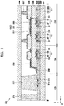
- FIG. 3 is a cross-sectional view taken along sectional line III-III' of the display panel of FIG. 2 , according to one or more exemplary embodiments.
- the display panel 200 may include the substrate 201 and the encapsulation portion 208 arranged on the substrate 201.
- the substrate 201 may be a glass substrate having rigidity or a plastic substrate. It is also contemplated that the substrate 201 may be a film having flexibility.
- the substrate 201 may be transparent, opaque, or semitransparent.
- the active area 220, a circuit area CA extending out of the active area 220, and a cell seal area CSA extending out of the circuit area CA are arranged on the substrate 201.
- the active area 220 may include an area for displaying an image, in which a display device, for example, an organic light-emitting display device (OLED), may be arranged.
- a display device for example, an organic light-emitting display device (OLED)
- OLED organic light-emitting display device
- a plurality of circuit wires (or transmission lines) for transmitting electric signals to the elements in the active area 220 may be arranged in the circuit area CA.
- the seal portion 211 for sealing an inner space between the substrate 201 and the encapsulation portion 208 may be arranged in the cell seal area CSA.
- a barrier film 202 may be arranged on the substrate 201.
- the barrier film 202 may planarize a surface of the substrate 201 and prevent (or at least reduce) intrusion of moisture or external air.
- the barrier film 202 may be an inorganic film and may be a single layer film or a multilayer film.
- a plurality of thin film transistors T1 and T2 and a storage capacitor Cst may be arranged in the active area 220.
- a first thin film transistor T1 may be a driving thin film transistor
- a second thin film transistor T2 may be a switching thin film transistor. Exemplary embodiments, however, are not limited thereto or thereby. It is also contemplated that additional thin film transistors and/or storage capacitors may be arranged in the active area 220.
- the first thin film transistor T1 may include a first semiconductor layer A1, a first gate electrode G1, a first source electrode S1, and a first drain electrode D1.
- the second thin film transistor T2 may include a second semiconductor layer A2, a second gate electrode G2, a second source electrode S2, and a second drain electrode D2.
- the first and second semiconductor layers A1 and A2 may be arranged on the barrier film 202.
- the first and second semiconductor layers A1 and A2 may include at least one of amorphous silicon, polysilicon, and an organic semiconductor material. It is also contemplated that the first and second semiconductor layers A1 and A2 may be formed of an oxide semiconductor material.
- the first and second semiconductor layers A1 and A2 may include a channel region that spaces a source region from a drain region. For instance, the source region and the drain region may be arranged at opposing sides of the channel region and may be doped with impurities.
- the gate insulating film 203 may be arranged on the first and second semiconductor layers A1 and A2.
- the gate insulating film 203 may be an inorganic film and may be a single layer film or a multilayer film.
- the first and second gate electrodes G1 and G2 may be arranged on the gate insulating film 203.
- the first and second gate electrodes G1 and G2 may be formed of a conductive material, such as a conductive metal material.
- the first and second gate electrodes G1 and G2 may include at least one of molybdenum (Mo), aluminum (Al), copper (Cu), and titanium (Ti). It is contemplated, however, that any suitable material may be utilized in association with exemplary embodiments.
- the first and second gate electrodes G1 and G2 may be a single layer film or a multilayer film.
- An interlayer insulating film 204 may be arranged on the first and second gate electrodes G1 and G2.
- the interlayer insulating film 204 may be an inorganic film.
- the interlayer insulating film 204 may be a single layer film or a multilayer film.
- the first and second source electrodes S1 and S2 and the first and second drain electrodes D1 and D2 may be arranged on the interlayer insulating film 204.
- Contact holes may be formed by removing parts of the gate insulating film 203 and parts of the interlayer insulating film 204. In this manner, the first and second source electrodes S1 and S2 and the first and second drain electrodes D1 and D2 may be electrically connected to corresponding source regions and drain regions of the first and second semiconductor layers A1 and A2 via the contact holes.
- the first and second source electrodes S1 and S2 and the first and second drain electrodes D1 and D2 may be formed of a conductive material, such as a conductive metal material.
- the first and second source electrodes S1 and S2 and the first and second drain electrodes D1 and D2 may include at least one Mo, A1, Cu, and Ti. It is contemplated, however, that any suitable material may be utilized in association with exemplary embodiments.
- the first and second source electrodes S1 and S2 and the first and second drain electrodes D1 and D2 may be single layer films or multilayer films.
- the first and second source electrodes S1 and S2 and the first and second drain electrodes D1 and D2 may have a stack structure of Ti/ Al/Ti.
- a protective film 205 may be arranged on the first and second source electrodes S1 and S2 and the first and second drain electrodes D1 and D2.
- the protective film 205 may be an organic film or an inorganic film.
- the protective film 205 may be (or include) a passivation film and/or a planarization film. In this manner, any one of the passivation film and the planarization film may be omitted.
- the first electrode 231 is a pixel electrode and may be formed of various conductive materials.
- the first electrode 231 may include a transparent electrode or a reflective electrode.
- the first electrode 231 may include a transparent conductive film.
- the first electrode 231 may include a reflective film and a transparent conductive film arranged on the reflective film.
- a pixel defining layer 206 may be arranged on the protective film 205.
- the pixel defining layer 206 may cover a portion of the first electrode 231.
- the pixel defining layer 206 defines a light-emitting area for each pixel (or sub-pixels) by encompassing an edge of the first electrode 231.
- the first electrode 231 may be patterned for each sub-pixel, and the pixel defining layer 206 may include corresponding patterned regions overlapping the sub-pixel patterns of the first electrode 231.
- the pixel defining layer 206 may be an organic film and may be a single layer film or a multilayer film.
- An intermediate layer 232 may be arranged on the first electrode 231 in an area exposed by etching a portion of the pixel defining layer 206.
- the intermediate layer 232 may include an organic emissive layer. It is also contemplated that the intermediate layer 232 may include an organic emissive layer and may further include at least one of a hole injection layer (HIL), a hole transport layer (HTL), an electron transport layer (ETL), and an electron injection layer (EIL). In one or more exemplary embodiments, the intermediate layer 232 may further include various functional layers, in addition to the organic emissive layer.
- the second electrode 233 may be arranged on the intermediate layer 232.
- the second electrode 233 may be a counter electrode.
- the second electrode 233 may include a transparent electrode or a reflective electrode.
- the second electrode 233 may include a metal film and a transparent conductive film arranged on the metal film.
- the second electrode 233 may include a metal film.
- a plurality of sub-pixels may be formed on the substrate 201.
- each sub-pixel may emit a red color, a green color, a blue color, or a white color. It is contemplated, however, that exemplary embodiments are not limited thereto or thereby. In this manner, any suitable color may be utilized in association with exemplary embodiments.
- a circuit wiring 210 may be arranged in the circuit area CA.
- the circuit wiring 210 may be arranged on the protective film 205.
- the circuit wiring 210 may be formed of the same material as the first electrode 231, however, exemplary embodiments are not limited thereto or thereby.
- the circuit wiring 210 may be electrically connected to the second electrode 233.
- the circuit wiring 210 may be connected to a power wiring 209.
- the power wiring 209 may be arranged on the interlayer insulating film 204.
- the power wiring 209 may be formed of the same material as the source electrode S3 and the drain electrode D3, but exemplary embodiments are not limited thereto or thereby.
- the power wiring 209 may be a wire through which an external power is applied.
- the power wiring 209 may be a triple layered structure of Ti/Al/Ti.
- One end of the circuit wiring 210 may contact the power wiring 209.
- at least a portion of the circuit wiring 210 may overlap the power wiring 209.
- An opening 214 may be arranged in the interlayer insulating film 204 covering the metal pattern layer 213.
- the opening 214 may be formed to increase a contact area between the interlayer insulating film 204 and the seal portion 211. In this manner, a combination strength between the interlayer insulating film 204 and the seal portion 211 may be improved.
- the seal portion 211 may be arranged on opposing surfaces of the substrate 201 and the encapsulation portion 208 that facing each other.
- the seal portion 211 may be formed along an area in which the substrate 201 and the encapsulation portion 208 overlap each other. In this manner, the seal portion 211 may encompass an edge of the active area 220.
- At least one dummy seal portion 212 may be arranged around the seal portion 211.
- the dummy seal portion 212 may be arranged, as seen in FIG. 2 , between the seal portion 211 and the boundary line BL.
- the dummy seal portion 212 may be formed of the same material as the seal portion 211.
- the dummy seal portion 212 may include frit glass.
- a cutting line CL may be arranged on the seal portion 211.
- the cutting line CL may be a cutting portion for splitting the substrate 201 into a plurality of separate display devices.
- the substrate 201 may be a mother substrate.
- a pattern corresponding to each display device may be formed on the substrate 201, and then the substrate 201 may be cut into separate display devices using at least one of a cutting wheel, a laser device, or the like.
- the display panel 200 may be cut on the seal portion 211 to reduce dead space.
- the cutting line CL may be located in an area in which the substrate 201, the encapsulation portion 208, and the seal portion 211 overlap one another in a perpendicular direction to the display panel 200, such as a second direction (e.g., the Z direction), which may be perpendicular to the first direction and a third direction (e.g., the X direction).
- the display panel 200 may be cut along the cutting line CL.
- the cutting line CL may correspond to an edge 201a of the substrate 201.
- an inflection point may be generated at a boundary between an area where the seal portion 211 is arranged and an area where the seal portion 211 is not arranged with respect to the boundary line BL in the area where the substrate 201 and the encapsulation portion 208 overlap each other. In this manner, the display panel 200 may be damaged at (or around) the boundary line BL.
- At least a portion 216a of each of the signal lines 216 may be arranged in the area defined by the distance d between the outer edge 211a of the seal portion 211 and the boundary line BL in the area where the substrate 201 and the encapsulation portion 208 overlap each other.
- the area defined by the distance d may be an area where the portion 216a of each of the signal lines 216 drawn from the active area 220 and the circuit area CA are arranged.
- the area defined by the distance d may be a space for escaping thermal deformation of the signal lines 216.
- the distance d may be an allowable space used when the substrate 201 and the encapsulation portion 208 are combined with each other with respect to the seal portion 211 disposed therebetween.
- the signal lines 216 may be arranged in the first direction (e.g., Y direction) of the display panel 200 across the boundary line BL of the area where the substrate 201 and the encapsulation portion 208 overlap each other.
- the dummy seal portion 212 may be arranged inside the cutting line CL. In one or more exemplary embodiments, the dummy seal portion 212 may be spaced apart from the seal portion 211.
- the dummy seal portion 212 has an island shape when viewed in the second direction (e.g., Z direction). When the display panel 200 is rectangular when viewed in the second direction, the seal portion 211 may have a rectangular band shape encompassing the active area 220 when viewed in the second direction, and the dummy seal portion 212 may have at least one dot pattern spaced apart from the seal portion 211 when viewed in the second direction.
- the dummy seal portion 212 may be arranged close to the cutting line CL, a cutting defect due to a step between the area where the seal portion 211 is arranged and the area where the seal portion 211 is not arranged when the display panel 200 is cut along the cutting line CL may be prevented or reduced.
- the dummy seal portion 212 may be arranged between the signal lines 216 and the cutting line CL.
- the dummy seal portion 212 may be arranged between the outermost signal line of the signal lines 216 in the third direction (e.g., X direction) and the cutting line CL. It is noted, however, that the position of the dummy seal portion 212 may be changed in any suitable manner according to exemplary embodiments.
- a display panel 400 may include a substrate 401 and an encapsulation portion 408.
- a plurality of pad terminals 415 may be arranged in an exposed area 417 of the substrate 401 extending out of an area where the substrate 401 and the encapsulation portion 408 overlap each other.
- the pad terminals 415 may be electrically connected to an active area 420 by a plurality of signal lines 416.
- a seal portion 411 may be arranged between the substrate 401 and the encapsulation portion 408.
- the seal portion 411 may be formed in the area where the substrate 401 and the encapsulation portion 408 overlap each other. In one or more exemplary embodiments, the seal portion 411 encompasses an edge of the active area 420.
- the cutting line CL may be arranged on the seal portion 411.
- the cutting line CL may be located in an area where the substrate 401, the encapsulation portion 408, and the seal portion 411 overlap one another in a direction perpendicular to the display panel 400, e.g., the Z direction.
- the cutting line CL may correspond to an edge 401a of the substrate 401.
- a dummy seal portion 412 may be arranged outside the seal portion 411.
- the dummy seal portion 412 may be arranged in an area defined by a distance d between an outer edge 411a of the seal portion 411 and the boundary line BL in the area where the substrate 401 and the encapsulation portion 408 overlap each other.
- the dummy seal portion 412 may be arranged at (or near) a corner C of the area where the substrate 401 and the encapsulation portion 408 overlap each other.
- At least a portion 416a of the signal lines 416 may be arranged in the area defined by a distance d between the outer edge 411a of the seal portion 411 and the boundary line BL in the area where the substrate 401 and the encapsulation portion 408 overlap each other.
- the signal lines 416 may be arranged in a Y direction of the display panel 400 across the boundary line BL of the area where the substrate 401 and the encapsulation portion 408 overlap each other.
- the dummy seal portion 412 may contact the cutting line CL.
- a part of the dummy seal portion 412 may be cut with a part of the seal portion 411.
- the part of the dummy seal portion 412 that is cut may be a tolerance generated when the dummy seal portion 412 is patterned using a seal patterning mask.
- the dummy seal portion 412 may be arranged between the signal lines 416 and the cutting line CL.
- FIG. 5 is a partially enlarged plan view of a portion of a display panel, according to one or more exemplary embodiments.
- the display panel 500 of FIG. 5 is similar to the display panel 200 of FIGS. 1 to 3 and the display panel 400 of FIG. 4 , and, as such, duplicative descriptions will be primarily omitted to avoid obscuring exemplary embodiments.
- a display panel 500 may include a substrate 501 and an encapsulation portion 508.
- a plurality of pad terminals 515 may be arranged in an exposed area 517 of the substrate 501.
- the pad terminals 515 may be electrically connected to an active area 520 by a plurality of signal lines 516.
- a seal portion 511 may be arranged between the substrate 501 and the encapsulation portion 508. In one or more exemplary embodiments, the seal portion 511 encompasses an edge of the active area 520.
- the cutting line CL may be arranged on the seal portion 511. The cutting line CL may correspond to an edge 501a of the substrate 501.
- a dummy seal portion 512 may be arranged outside the seal portion 511.
- the dummy seal portion 512 may be arranged in an area defined by a distance d between an outer edge 511a of the seal portion 511 and the boundary line BL of an area where the substrate 501 and the encapsulation portion 508 overlap each other.
- At least a part 516a of each of the signal lines 516 may be arranged in the area defined by the distance d.
- the dummy seal portion 512 may be connected to the seal portion 511. At least a part 512a of the dummy seal portion 512 may be connected to the outer edge 511a of the seal portion 511. The part 512a of the dummy seal portion 512 may be connected to the seal portion 511 as the dummy seal portion 512 having a dot shape extends during patterning using a seal patterning mask. In one or more exemplary embodiments, the dummy seal portion 512 may be arranged between the signal lines 516 and the cutting line CL.
- seal portions 211, 411, or 511 A process of manufacturing separate display devices by cutting a display panel on a seal portion, such as seal portions 211, 411, or 511, will be described below.
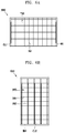
- FIG. 6A to 6G sequentially illustrate a process of manufacturing a plurality of unit display panels 700, according to one or more exemplary embodiments.
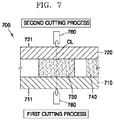
- FIG. 7 is a cross-sectional view of cutting a display panel on a seal portion, according to one or more exemplary embodiments.
- a mother substrate 600 is prepared.
- the mother substrate 600 may be a substrate used to simultaneously manufacture the unit display panels 700.
- the unit display panels 700 may be patterned on a first surface 601 of the mother substrate 600 and may be spaced apart from one another.
- Each of the unit display panels 700 may include a substrate 710 (see FIG. 7 ), on which a display portion, such as a thin film transistor or an organic light-emitting display device is patterned, and a seal substrate 720 (see FIG. 7 ) arranged above the substrate 710.
- the unit display panels 700 are cut on the first surface 601 of the mother substrate 600 along first cutting lines CL1 extending in a vertical direction at horizontally opposite edges of the unit display panels 700.
- the first surface 601 of the mother substrate 600 may be a surface on which the substrate 710 of FIG. 7 is arranged.
- the unit display panels 700 may be cut in a thickness direction of the mother substrate 600 from the first surface 601 of the mother substrate 600 towards a second surface 602 (see FIG. 6C ) of the mother substrate 600 opposing the first surface 601 in the thickness direction of the mother substrate 600.
- a depth of the cuts in the thickness direction may be about half the thickness of the mother substrate 600.
- the unit display panels 700 may be cut on the first surface 601 of the mother substrate 600 along second cutting lines CL2 extending in a horizontal direction and corresponding to second edges 702 of each of the unit display panels 700.
- the unit display panels 700 may be cut in the thickness direction of the mother substrate 600 from the first surface 601 of the mother substrate 600 towards a second surface 602 (see FIG. 6C ) of the mother substrate 600 opposing the first surface 601 in the thickness direction of the mother substrate 600.
- a depth of the cuts in the thickness direction may be about half the thickness of the mother substrate 600.
- the unit display panels 700 are cut on the second surface 602 of the mother substrate 600 along third cutting lines CL3 extending in the vertical direction at the horizontally opposite edges of the unit display panels 700.
- the second surface 602 of the mother substrate 600 may be a surface opposite to the first surface 601 of the mother substrate 600.
- the second surface 602 of the mother substrate 600 may be a surface on which the seal substrate 720 of FIG. 7 is arranged.
- the third cutting line CL3 may correspond to (e.g., overlap) the first cutting lines CL1.
- the unit display panels 700 may be cut in the thickness direction of the mother substrate 600 from the second surface 602 of the mother substrate 600 toward the first surface 601 of the mother substrate 600.
- a depth of the cuts in the thickness direction may be about half the thickness of the mother substrate 600.
- the horizontally opposite peripheral edge portions 670 of the mother substrate 600 may be cut from a central portion of the mother substrate 600.
- the unit display panels 700 are cut on the second surface 602 of the mother substrate 600 along fourth cutting lines CL4 extending in the horizontal direction and corresponding to a second edge 702 of each of the unit display panels 700.
- the fourth cutting lines CL4 may correspond to (e.g., overlap) the second cutting lines CL2.
- the unit display panels 700 may be cut in the thickness direction of the mother substrate 600 from the second surface 602 of the mother substrate 600 toward the first surface 601 of the mother substrate 600.
- a depth of the cuts in the thickness direction may be about half the thickness of the mother substrate 600.
- the mother substrate 600 may be split into a plurality of unit sticks 660 of unit display panels 700.
- An exemplary unit stick 660 of unit display panels 700 is illustrated in FIG. 6E .
- the unit stick 660 may include the unit display panels 700 arranged in a same line, e.g., row of unit display panels 700 of a matrix of unit display panels 700 formed on mother substrate 600.
- the unit display panels 700 are cut on a first surface 661 of the unit sticks 660 along fifth cutting lines CL5 corresponding to the first edge 701 of each of the unit display panels 700.
- the first surface 661 of each of the unit sticks 660 may be a surface on which the substrate 710 of FIG. 7 is arranged.
- the first surface 661 of the unit sticks 660 may correspond to the first surface 601 of the mother substrate 600.
- the unit display panels 700 may be cut in a thickness direction of each of the unit sticks 660 from the first surface 661 of each of the unit sticks 660 toward a second surface 662 (see FIG. 6F ) of each of the unit sticks 660.
- a depth of the cuts in the thickness direction may be about half the thickness of the unit sticks 660.
- the unit display panels 700 are cut on a second surface 662 of each of the unit sticks 660 along sixth cutting lines CL6 corresponding to the first edge 701 of each of the unit display panels 700.
- the second surface 662 of each of the unit sticks 660 is a surface opposite the first surface 661 of each of the unit sticks 660.
- the second surface 662 of each of the unit sticks 660 may correspond to the second surface 602 of the mother substrate 600.
- the second surface 662 of each of the unit sticks 660 may be a surface on which the seal substrate 720 of FIG. 7 is arranged.
- the unit display panels 700 may be cut in the thickness direction of each of the unit sticks 660 from the second surface 662 of each of the unit sticks 660 toward the first surface 661 of each of the unit sticks 660.
- a depth of the cuts in the thickness direction may be about half the thickness of the unit sticks 660.
- separate unit display devices 700 may be manufactured, as illustrated in FIG. 6G .
- FIG. 7 is a cross-sectional view of cutting a display panel on a seal portion, according to one or more exemplary embodiments.
- each of the unit display panels 700 may include the substrate 710 on which the display portion, which may include one or more thin film transistors and/or one or more organic light-emitting display devices, is patterned, and the seal substrate 720 arranged above the substrate 710.
- the unit display panels 700 may be cut on the substrate 710 using a cutting wheel 760 or any other suitable cutting mechanism, e.g., laser, etc.
- the cutting wheel 760 cuts the substrate 710 in a thickness direction of the substrate 710 from a surface 711 of the substrate 710 towards seal portion 730.
- FIG. 7 illustrates that the cutting wheel 760 starts cutting from a lower surface of the substrate 710 for convenience of explanation, the cutting wheel 760 may start cutting from an upper surface of the substrate 710.
- the unit display panels 700 may be cut on the seal substrate 720 using the cutting wheel 760 or any other suitable cutting mechanism, such as a laser, etc.
- the cutting wheel 760 cuts the seal substrate 720 in a thickness direction of the seal substrate 720 from a surface 721 of the seal substrate 720 towards the seal portion 730.
- about the other half of the thickness of the seal portion 730 may be cut in the thickness direction by the cutting wheel 760.
- the unit display panels 700 may be completely cut on the seal portion 730.
- damage to the unit display panels 700 may be prevented or at least reduced.
- a dummy seal portion arranged near a seal portion of a display device may be utilized to reduce (or prevent) damage to a substrate of the display device.
Landscapes
- Physics & Mathematics (AREA)
- Optics & Photonics (AREA)
- Engineering & Computer Science (AREA)
- Microelectronics & Electronic Packaging (AREA)
- Manufacturing & Machinery (AREA)
- Electroluminescent Light Sources (AREA)
- Devices For Indicating Variable Information By Combining Individual Elements (AREA)
Claims (12)
- Anzeigevorrichtung (100), umfassend:ein Substrat (201);einen Verkapselungsabschnitt (208) auf dem Substrat (201);einen Dichtungsabschnitt (211) zwischen dem Substrat (201) und dem Verkapselungsabschnitt (208); undmindestens einen Dummydichtungsabschnitt (212) benachbart zu dem Dichtungsabschnitt (211),wobei:das Substrat (201) und der Verkapselungsabschnitt (208) sich in einer ersten Richtung, die senkrecht zu einer Oberfläche des Substrats (201) verläuft, mindestens teilweise überlappen; undder Dummydichtungsabschnitt (212), in der ersten Richtung betrachtet, in einem Bereich zwischen einem Rand des Dichtungsabschnitts (211) und einer Grenzlinie eines überlappenden Bereichs des Substrats (201) und des Verkapselungsabschnitts (208) angeordnet ist, wobei:der Dichtungsabschnitt (211), in der ersten Richtung betrachtet, einen aktiven Bereich (220) des Substrats (201) umschließt; undder Dummydichtungsabschnitt (212), in der ersten Richtung betrachtet, außerhalb des aktiven Bereichs (220) und des Dichtungsabschnitts (211) angeordnet ist,wobei, in der ersten Richtung betrachtet:ein Bereich des Substrats (201) sich über die Grenzlinie hinaus erstreckt;Kontaktflächenanschlüsse (215) in dem Bereich, der sich über die Grenzlinie hinaus erstreckt, angeordnet sind;Signalleitungen (216) jeweils mit den Kontaktflächenanschlüssen (215) verbunden sind; unddie Signalleitungen (216) die Grenzlinie kreuzen, wobei:der Dummydichtungsabschnitt (212), in der ersten Richtung betrachtet, von dem Dichtungsabschnitt (211) beabstandet ist;dadurch gekennzeichnet, dass der Dummydichtungsabschnitt (212) mindestens eine Inselform umfasst.
- Anzeigevorrichtung (100) nach Anspruch 1, wobei, in der ersten Richtung betrachtet, der Dummydichtungsabschnitt (212) relativ näher an mindestens einer Ecke des überlappenden Bereichs als der aktive Bereich (220) angeordnet ist.
- Anzeigevorrichtung (100) nach Anspruch 1, wobei der Dummydichtungsabschnitt (212) eine Mehrzahl strukturierter Inselformen umfasst.
- Anzeigevorrichtung (100) nach Anspruch 2, wobei der Dummydichtungsabschnitt (212) mit einem Rand des Substrats (201) in Kontakt steht.
- Anzeigevorrichtung (100) nach Anspruch 2, wobei der Dummydichtungsabschnitt (512) mit dem Rand des Dichtungsabschnitts (511) verbunden ist.
- Anzeigevorrichtung (100) nach Anspruch 1, wobei der Bereich, der sich über die Grenzlinie hinaus erstreckt, einem Bereich des Substrats (201) entspricht, wobei, in der ersten Richtung betrachtet, jeweilige Abschnitte der Signalleitungen (216) in dem Bereich zwischen dem Rand des Dichtungsabschnitts (211) und der Grenzlinie des überlappenden Bereichs des Substrats (201) und des Verkapselungsabschnitts (208) angeordnet sind, und/oder
wobei:mindestens eine andere Anzeigevorrichtung (100) das Substrat (201) umfasst; undeine Schnittlinie zum Abtrennen der Anzeigevorrichtung (100) von der mindestens einen anderen Anzeigevorrichtung (100), in der ersten Richtung betrachtet, den Dichtungsabschnitt (211) überlappt. - Anzeigevorrichtung (100) nach Anspruch 6, wobei, in der ersten Richtung betrachtet, das Substrat (201), der Verkapselungsabschnitt (208) und der Dichtungsabschnitt (211) sich entlang eines Abschnitts der Schnittlinie überlappen, wobei die Schnittlinie einem Rand der Anzeigevorrichtung (100) entspricht, und/oder
wobei, in der ersten Richtung betrachtet, der Dummydichtungsabschnitt (212) zwischen der Schnittlinie und dem Rand des Dichtungsabschnitts (211) angeordnet ist. - Anzeigevorrichtung (100) nach Anspruch 7, wobei:
der Dummydichtungsabschnitt (212), in der ersten Richtung betrachtet, von dem Dichtungsabschnitt (211) beabstandet ist. - Anzeigevorrichtung (100) nach Anspruch 8, wobei der Dummydichtungsabschnitt (212) eine Mehrzahl strukturierter Inselformen umfasst.
- Anzeigevorrichtung (100) nach Anspruch 7, wobei mindestens ein Teil des Dummydichtungsabschnitts (512) mit dem äußeren Rand (511a) des Dichtungsabschnitts (511) verbunden ist.
- Anzeigevorrichtung (100) nach Anspruch 6, wobei, in der ersten Richtung betrachtet, die Schnittlinie sich durch den Dummydichtungsabschnitt (412) hindurch erstreckt.
- Anzeigevorrichtung (100) nach Anspruch 1, wobei das Substrat (201) Folgendes umfasst:einen aktiven Bereich (220) zum Anzeigen eines Bildes;einen Schaltungsbereich (CA), der sich von dem aktiven Bereich (220) aus erstreckt, wobei der Schaltungsbereich (CA) eine Schaltungsverdrahtung (210) umfasst; undeinen Zellabdichtungsbereich (CSA), der sich von dem Schaltungsbereich (CA) aus erstreckt, wobei der Zellabdichtungsbereich (CSA) den Dichtungsabschnitt (211) und den Dummydichtungsabschnitt (212) umfasst, und/oderwobei der Dummydichtungsabschnitt (212) Fritteglas umfasst.
Applications Claiming Priority (1)
| Application Number | Priority Date | Filing Date | Title |
|---|---|---|---|
| KR1020160085066A KR102570551B1 (ko) | 2016-07-05 | 2016-07-05 | 디스플레이 장치 |
Publications (2)
| Publication Number | Publication Date |
|---|---|
| EP3267490A1 EP3267490A1 (de) | 2018-01-10 |
| EP3267490B1 true EP3267490B1 (de) | 2021-02-24 |
Family
ID=59296744
Family Applications (1)
| Application Number | Title | Priority Date | Filing Date |
|---|---|---|---|
| EP17179767.3A Active EP3267490B1 (de) | 2016-07-05 | 2017-07-05 | Anzeigevorrichtung |
Country Status (4)
| Country | Link |
|---|---|
| US (1) | US10170728B2 (de) |
| EP (1) | EP3267490B1 (de) |
| KR (1) | KR102570551B1 (de) |
| CN (1) | CN107579162B (de) |
Families Citing this family (7)
| Publication number | Priority date | Publication date | Assignee | Title |
|---|---|---|---|---|
| KR102566157B1 (ko) * | 2018-06-28 | 2023-08-11 | 삼성디스플레이 주식회사 | 표시장치 |
| CN109671865B (zh) * | 2018-12-21 | 2022-02-01 | 厦门天马微电子有限公司 | 显示面板及显示装置 |
| US11264582B2 (en) * | 2019-03-03 | 2022-03-01 | Innolux Corporation | Light emitting device |
| KR102823250B1 (ko) | 2019-08-20 | 2025-06-20 | 삼성디스플레이 주식회사 | 표시 장치 및 그 제조 방법 |
| CN110867136B (zh) | 2019-11-22 | 2021-10-15 | 维沃移动通信有限公司 | 极点屏及电子设备 |
| KR102903711B1 (ko) * | 2020-06-02 | 2025-12-24 | 삼성디스플레이 주식회사 | 표시 장치 |
| KR20220000440A (ko) * | 2020-06-25 | 2022-01-04 | 삼성디스플레이 주식회사 | 표시 장치 및 표시 장치의 제조 방법 |
Citations (1)
| Publication number | Priority date | Publication date | Assignee | Title |
|---|---|---|---|---|
| US20150048330A1 (en) * | 2013-08-14 | 2015-02-19 | Samsung Display Co., Ltd. | Organic light-emitting display apparatus and method of manufacturing the same |
Family Cites Families (13)
| Publication number | Priority date | Publication date | Assignee | Title |
|---|---|---|---|---|
| JPH0822013A (ja) * | 1994-07-08 | 1996-01-23 | Mitsubishi Electric Corp | 液晶表示素子及びその製造方法 |
| JP2001281675A (ja) | 2000-03-29 | 2001-10-10 | Matsushita Electric Ind Co Ltd | 液晶表示装置の製造方法 |
| US6879110B2 (en) * | 2000-07-27 | 2005-04-12 | Semiconductor Energy Laboratory Co., Ltd. | Method of driving display device |
| US7351300B2 (en) * | 2001-08-22 | 2008-04-01 | Semiconductor Energy Laboratory Co., Ltd. | Peeling method and method of manufacturing semiconductor device |
| KR100798310B1 (ko) | 2001-08-24 | 2008-01-28 | 엘지.필립스 엘시디 주식회사 | 액정 표시장치의 실 패터닝방법 및 실패턴 |
| JP2008096836A (ja) | 2006-10-13 | 2008-04-24 | Sharp Corp | 液晶表示パネルの製造方法、および液晶表示パネル |
| JP2011107556A (ja) | 2009-11-20 | 2011-06-02 | Technology Research Association For Advanced Display Materials | 表示装置の製造方法及び表示装置 |
| KR101813906B1 (ko) * | 2011-03-15 | 2018-01-03 | 삼성디스플레이 주식회사 | 디스플레이 패널 |
| TWI451610B (zh) | 2011-05-17 | 2014-09-01 | Au Optronics Corp | 發光裝置之母板結構以及發光裝置及其製造方法 |
| KR20150043605A (ko) * | 2013-10-11 | 2015-04-23 | 삼성디스플레이 주식회사 | 유기 발광 표시 장치 및 유기 발광 표시 패널의 절단 방법 |
| KR102147964B1 (ko) | 2014-01-03 | 2020-08-25 | 삼성전자주식회사 | 개선된 디스플레이 조립 구조를 갖는 전자 장치 |
| KR102210523B1 (ko) * | 2014-07-17 | 2021-02-02 | 삼성디스플레이 주식회사 | 표시장치 및 이의 제조방법 |
| KR102223679B1 (ko) * | 2014-08-04 | 2021-03-08 | 삼성디스플레이 주식회사 | 디스플레이 패널 및 이를 제조하기 위한 모패널 |
-
2016
- 2016-07-05 KR KR1020160085066A patent/KR102570551B1/ko active Active
-
2017
- 2017-02-21 US US15/437,671 patent/US10170728B2/en active Active
- 2017-07-05 CN CN201710542309.7A patent/CN107579162B/zh active Active
- 2017-07-05 EP EP17179767.3A patent/EP3267490B1/de active Active
Patent Citations (1)
| Publication number | Priority date | Publication date | Assignee | Title |
|---|---|---|---|---|
| US20150048330A1 (en) * | 2013-08-14 | 2015-02-19 | Samsung Display Co., Ltd. | Organic light-emitting display apparatus and method of manufacturing the same |
Also Published As
| Publication number | Publication date |
|---|---|
| CN107579162A (zh) | 2018-01-12 |
| EP3267490A1 (de) | 2018-01-10 |
| CN107579162B (zh) | 2021-07-02 |
| US10170728B2 (en) | 2019-01-01 |
| US20180013094A1 (en) | 2018-01-11 |
| KR102570551B1 (ko) | 2023-08-25 |
| KR20180005325A (ko) | 2018-01-16 |
Similar Documents
| Publication | Publication Date | Title |
|---|---|---|
| KR102798596B1 (ko) | 표시 장치 | |
| KR102906638B1 (ko) | 디스플레이 장치 및 전자 장치 | |
| US12089434B2 (en) | Organic light-emitting display apparatus and fabrication method thereof | |
| US10170728B2 (en) | Display device | |
| US11925066B2 (en) | Display device | |
| EP3678202B1 (de) | Anzeigesubstrat und herstellungsverfahren dafür sowie anzeigevorrichtung | |
| US10206276B2 (en) | Flexible display and method of manufacturing the same | |
| US10014491B2 (en) | Organic light-emitting diode display and manufacturing method thereof | |
| US10629855B2 (en) | Mask for manufacturing an organic light emitting display device, the mask including plurality of bridges to connect blocking plate to mask body | |
| US10446786B2 (en) | Display device and manufacturing method thereof | |
| KR20180005779A (ko) | 플렉서블 디스플레이 장치 | |
| US20220199920A1 (en) | Display panel, display apparatus, and method of manufacturing display apparatus | |
| CN114551530A (zh) | 显示设备 | |
| US11963431B2 (en) | Mask, flexible display panel and manufacturing method thereof | |
| US11545079B2 (en) | Display device and manufacturing method of the same | |
| US12396332B2 (en) | Electronic device and method of manufacturing the same | |
| US12193285B2 (en) | Display panel, display device including the same, and method of manufacturing the same | |
| US20240260436A1 (en) | Display panel and manufacturing method of the same | |
| CN121463671A (zh) | 显示面板及显示装置 | |
| KR20260007467A (ko) | 표시 패널 및 이를 포함하는 전자 기기 |
Legal Events
| Date | Code | Title | Description |
|---|---|---|---|
| PUAI | Public reference made under article 153(3) epc to a published international application that has entered the european phase |
Free format text: ORIGINAL CODE: 0009012 |
|
| STAA | Information on the status of an ep patent application or granted ep patent |
Free format text: STATUS: THE APPLICATION HAS BEEN PUBLISHED |
|
| STAA | Information on the status of an ep patent application or granted ep patent |
Free format text: STATUS: REQUEST FOR EXAMINATION WAS MADE |
|
| AK | Designated contracting states |
Kind code of ref document: A1 Designated state(s): AL AT BE BG CH CY CZ DE DK EE ES FI FR GB GR HR HU IE IS IT LI LT LU LV MC MK MT NL NO PL PT RO RS SE SI SK SM TR |
|
| AX | Request for extension of the european patent |
Extension state: BA ME |
|
| 17P | Request for examination filed |
Effective date: 20171218 |
|
| RBV | Designated contracting states (corrected) |
Designated state(s): AL AT BE BG CH CY CZ DE DK EE ES FI FR GB GR HR HU IE IS IT LI LT LU LV MC MK MT NL NO PL PT RO RS SE SI SK SM TR |
|
| STAA | Information on the status of an ep patent application or granted ep patent |
Free format text: STATUS: EXAMINATION IS IN PROGRESS |
|
| 17Q | First examination report despatched |
Effective date: 20180705 |
|
| GRAP | Despatch of communication of intention to grant a patent |
Free format text: ORIGINAL CODE: EPIDOSNIGR1 |
|
| STAA | Information on the status of an ep patent application or granted ep patent |
Free format text: STATUS: GRANT OF PATENT IS INTENDED |
|
| INTG | Intention to grant announced |
Effective date: 20200916 |
|
| GRAS | Grant fee paid |
Free format text: ORIGINAL CODE: EPIDOSNIGR3 |
|
| GRAA | (expected) grant |
Free format text: ORIGINAL CODE: 0009210 |
|
| STAA | Information on the status of an ep patent application or granted ep patent |
Free format text: STATUS: THE PATENT HAS BEEN GRANTED |
|
| AK | Designated contracting states |
Kind code of ref document: B1 Designated state(s): AL AT BE BG CH CY CZ DE DK EE ES FI FR GB GR HR HU IE IS IT LI LT LU LV MC MK MT NL NO PL PT RO RS SE SI SK SM TR |
|
| REG | Reference to a national code |
Ref country code: CH Ref legal event code: EP |
|
| REG | Reference to a national code |
Ref country code: AT Ref legal event code: REF Ref document number: 1365570 Country of ref document: AT Kind code of ref document: T Effective date: 20210315 |
|
| REG | Reference to a national code |
Ref country code: IE Ref legal event code: FG4D |
|
| REG | Reference to a national code |
Ref country code: DE Ref legal event code: R096 Ref document number: 602017033093 Country of ref document: DE |
|
| REG | Reference to a national code |
Ref country code: NL Ref legal event code: FP |
|
| REG | Reference to a national code |
Ref country code: LT Ref legal event code: MG9D |
|
| PG25 | Lapsed in a contracting state [announced via postgrant information from national office to epo] |
Ref country code: FI Free format text: LAPSE BECAUSE OF FAILURE TO SUBMIT A TRANSLATION OF THE DESCRIPTION OR TO PAY THE FEE WITHIN THE PRESCRIBED TIME-LIMIT Effective date: 20210224 Ref country code: GR Free format text: LAPSE BECAUSE OF FAILURE TO SUBMIT A TRANSLATION OF THE DESCRIPTION OR TO PAY THE FEE WITHIN THE PRESCRIBED TIME-LIMIT Effective date: 20210525 Ref country code: HR Free format text: LAPSE BECAUSE OF FAILURE TO SUBMIT A TRANSLATION OF THE DESCRIPTION OR TO PAY THE FEE WITHIN THE PRESCRIBED TIME-LIMIT Effective date: 20210224 Ref country code: NO Free format text: LAPSE BECAUSE OF FAILURE TO SUBMIT A TRANSLATION OF THE DESCRIPTION OR TO PAY THE FEE WITHIN THE PRESCRIBED TIME-LIMIT Effective date: 20210524 Ref country code: PT Free format text: LAPSE BECAUSE OF FAILURE TO SUBMIT A TRANSLATION OF THE DESCRIPTION OR TO PAY THE FEE WITHIN THE PRESCRIBED TIME-LIMIT Effective date: 20210624 Ref country code: LT Free format text: LAPSE BECAUSE OF FAILURE TO SUBMIT A TRANSLATION OF THE DESCRIPTION OR TO PAY THE FEE WITHIN THE PRESCRIBED TIME-LIMIT Effective date: 20210224 Ref country code: BG Free format text: LAPSE BECAUSE OF FAILURE TO SUBMIT A TRANSLATION OF THE DESCRIPTION OR TO PAY THE FEE WITHIN THE PRESCRIBED TIME-LIMIT Effective date: 20210524 |
|
| REG | Reference to a national code |
Ref country code: AT Ref legal event code: MK05 Ref document number: 1365570 Country of ref document: AT Kind code of ref document: T Effective date: 20210224 |
|
| PG25 | Lapsed in a contracting state [announced via postgrant information from national office to epo] |
Ref country code: RS Free format text: LAPSE BECAUSE OF FAILURE TO SUBMIT A TRANSLATION OF THE DESCRIPTION OR TO PAY THE FEE WITHIN THE PRESCRIBED TIME-LIMIT Effective date: 20210224 Ref country code: PL Free format text: LAPSE BECAUSE OF FAILURE TO SUBMIT A TRANSLATION OF THE DESCRIPTION OR TO PAY THE FEE WITHIN THE PRESCRIBED TIME-LIMIT Effective date: 20210224 Ref country code: LV Free format text: LAPSE BECAUSE OF FAILURE TO SUBMIT A TRANSLATION OF THE DESCRIPTION OR TO PAY THE FEE WITHIN THE PRESCRIBED TIME-LIMIT Effective date: 20210224 Ref country code: SE Free format text: LAPSE BECAUSE OF FAILURE TO SUBMIT A TRANSLATION OF THE DESCRIPTION OR TO PAY THE FEE WITHIN THE PRESCRIBED TIME-LIMIT Effective date: 20210224 |
|
| PG25 | Lapsed in a contracting state [announced via postgrant information from national office to epo] |
Ref country code: IS Free format text: LAPSE BECAUSE OF FAILURE TO SUBMIT A TRANSLATION OF THE DESCRIPTION OR TO PAY THE FEE WITHIN THE PRESCRIBED TIME-LIMIT Effective date: 20210624 |
|
| PG25 | Lapsed in a contracting state [announced via postgrant information from national office to epo] |
Ref country code: EE Free format text: LAPSE BECAUSE OF FAILURE TO SUBMIT A TRANSLATION OF THE DESCRIPTION OR TO PAY THE FEE WITHIN THE PRESCRIBED TIME-LIMIT Effective date: 20210224 Ref country code: CZ Free format text: LAPSE BECAUSE OF FAILURE TO SUBMIT A TRANSLATION OF THE DESCRIPTION OR TO PAY THE FEE WITHIN THE PRESCRIBED TIME-LIMIT Effective date: 20210224 Ref country code: AT Free format text: LAPSE BECAUSE OF FAILURE TO SUBMIT A TRANSLATION OF THE DESCRIPTION OR TO PAY THE FEE WITHIN THE PRESCRIBED TIME-LIMIT Effective date: 20210224 Ref country code: SM Free format text: LAPSE BECAUSE OF FAILURE TO SUBMIT A TRANSLATION OF THE DESCRIPTION OR TO PAY THE FEE WITHIN THE PRESCRIBED TIME-LIMIT Effective date: 20210224 |
|
| REG | Reference to a national code |
Ref country code: DE Ref legal event code: R097 Ref document number: 602017033093 Country of ref document: DE |
|
| PG25 | Lapsed in a contracting state [announced via postgrant information from national office to epo] |
Ref country code: DK Free format text: LAPSE BECAUSE OF FAILURE TO SUBMIT A TRANSLATION OF THE DESCRIPTION OR TO PAY THE FEE WITHIN THE PRESCRIBED TIME-LIMIT Effective date: 20210224 Ref country code: RO Free format text: LAPSE BECAUSE OF FAILURE TO SUBMIT A TRANSLATION OF THE DESCRIPTION OR TO PAY THE FEE WITHIN THE PRESCRIBED TIME-LIMIT Effective date: 20210224 Ref country code: SK Free format text: LAPSE BECAUSE OF FAILURE TO SUBMIT A TRANSLATION OF THE DESCRIPTION OR TO PAY THE FEE WITHIN THE PRESCRIBED TIME-LIMIT Effective date: 20210224 |
|
| PLBE | No opposition filed within time limit |
Free format text: ORIGINAL CODE: 0009261 |
|
| STAA | Information on the status of an ep patent application or granted ep patent |
Free format text: STATUS: NO OPPOSITION FILED WITHIN TIME LIMIT |
|
| PG25 | Lapsed in a contracting state [announced via postgrant information from national office to epo] |
Ref country code: ES Free format text: LAPSE BECAUSE OF FAILURE TO SUBMIT A TRANSLATION OF THE DESCRIPTION OR TO PAY THE FEE WITHIN THE PRESCRIBED TIME-LIMIT Effective date: 20210224 Ref country code: AL Free format text: LAPSE BECAUSE OF FAILURE TO SUBMIT A TRANSLATION OF THE DESCRIPTION OR TO PAY THE FEE WITHIN THE PRESCRIBED TIME-LIMIT Effective date: 20210224 |
|
| 26N | No opposition filed |
Effective date: 20211125 |
|
| PG25 | Lapsed in a contracting state [announced via postgrant information from national office to epo] |
Ref country code: SI Free format text: LAPSE BECAUSE OF FAILURE TO SUBMIT A TRANSLATION OF THE DESCRIPTION OR TO PAY THE FEE WITHIN THE PRESCRIBED TIME-LIMIT Effective date: 20210224 |
|
| REG | Reference to a national code |
Ref country code: CH Ref legal event code: PL |
|
| PG25 | Lapsed in a contracting state [announced via postgrant information from national office to epo] |
Ref country code: MC Free format text: LAPSE BECAUSE OF FAILURE TO SUBMIT A TRANSLATION OF THE DESCRIPTION OR TO PAY THE FEE WITHIN THE PRESCRIBED TIME-LIMIT Effective date: 20210224 |
|
| REG | Reference to a national code |
Ref country code: BE Ref legal event code: MM Effective date: 20210731 |
|
| PG25 | Lapsed in a contracting state [announced via postgrant information from national office to epo] |
Ref country code: LI Free format text: LAPSE BECAUSE OF NON-PAYMENT OF DUE FEES Effective date: 20210731 Ref country code: IT Free format text: LAPSE BECAUSE OF FAILURE TO SUBMIT A TRANSLATION OF THE DESCRIPTION OR TO PAY THE FEE WITHIN THE PRESCRIBED TIME-LIMIT Effective date: 20210224 Ref country code: CH Free format text: LAPSE BECAUSE OF NON-PAYMENT OF DUE FEES Effective date: 20210731 |
|
| PG25 | Lapsed in a contracting state [announced via postgrant information from national office to epo] |
Ref country code: IS Free format text: LAPSE BECAUSE OF FAILURE TO SUBMIT A TRANSLATION OF THE DESCRIPTION OR TO PAY THE FEE WITHIN THE PRESCRIBED TIME-LIMIT Effective date: 20210624 Ref country code: LU Free format text: LAPSE BECAUSE OF NON-PAYMENT OF DUE FEES Effective date: 20210705 |
|
| PG25 | Lapsed in a contracting state [announced via postgrant information from national office to epo] |
Ref country code: IE Free format text: LAPSE BECAUSE OF NON-PAYMENT OF DUE FEES Effective date: 20210705 Ref country code: BE Free format text: LAPSE BECAUSE OF NON-PAYMENT OF DUE FEES Effective date: 20210731 |
|
| REG | Reference to a national code |
Ref country code: DE Ref legal event code: R079 Ref document number: 602017033093 Country of ref document: DE Free format text: PREVIOUS MAIN CLASS: H01L0027320000 Ipc: H10K0059000000 |
|
| PG25 | Lapsed in a contracting state [announced via postgrant information from national office to epo] |
Ref country code: HU Free format text: LAPSE BECAUSE OF FAILURE TO SUBMIT A TRANSLATION OF THE DESCRIPTION OR TO PAY THE FEE WITHIN THE PRESCRIBED TIME-LIMIT; INVALID AB INITIO Effective date: 20170705 |
|
| P01 | Opt-out of the competence of the unified patent court (upc) registered |
Effective date: 20230516 |
|
| PG25 | Lapsed in a contracting state [announced via postgrant information from national office to epo] |
Ref country code: CY Free format text: LAPSE BECAUSE OF FAILURE TO SUBMIT A TRANSLATION OF THE DESCRIPTION OR TO PAY THE FEE WITHIN THE PRESCRIBED TIME-LIMIT Effective date: 20210224 |
|
| PG25 | Lapsed in a contracting state [announced via postgrant information from national office to epo] |
Ref country code: MK Free format text: LAPSE BECAUSE OF FAILURE TO SUBMIT A TRANSLATION OF THE DESCRIPTION OR TO PAY THE FEE WITHIN THE PRESCRIBED TIME-LIMIT Effective date: 20210224 |
|
| PG25 | Lapsed in a contracting state [announced via postgrant information from national office to epo] |
Ref country code: MT Free format text: LAPSE BECAUSE OF FAILURE TO SUBMIT A TRANSLATION OF THE DESCRIPTION OR TO PAY THE FEE WITHIN THE PRESCRIBED TIME-LIMIT Effective date: 20210224 |
|
| PGFP | Annual fee paid to national office [announced via postgrant information from national office to epo] |
Ref country code: GB Payment date: 20250624 Year of fee payment: 9 |
|
| PGFP | Annual fee paid to national office [announced via postgrant information from national office to epo] |
Ref country code: NL Payment date: 20250623 Year of fee payment: 9 |
|
| PGFP | Annual fee paid to national office [announced via postgrant information from national office to epo] |
Ref country code: FR Payment date: 20250624 Year of fee payment: 9 |
|
| PGFP | Annual fee paid to national office [announced via postgrant information from national office to epo] |
Ref country code: DE Payment date: 20250624 Year of fee payment: 9 |
|
| PG25 | Lapsed in a contracting state [announced via postgrant information from national office to epo] |
Ref country code: TR Free format text: LAPSE BECAUSE OF FAILURE TO SUBMIT A TRANSLATION OF THE DESCRIPTION OR TO PAY THE FEE WITHIN THE PRESCRIBED TIME-LIMIT Effective date: 20210224 |