EP3264448A1 - Verfahren und system zur substratinspektion - Google Patents
Verfahren und system zur substratinspektion Download PDFInfo
- Publication number
- EP3264448A1 EP3264448A1 EP16755780.0A EP16755780A EP3264448A1 EP 3264448 A1 EP3264448 A1 EP 3264448A1 EP 16755780 A EP16755780 A EP 16755780A EP 3264448 A1 EP3264448 A1 EP 3264448A1
- Authority
- EP
- European Patent Office
- Prior art keywords
- interest
- region
- image
- substrate
- good
- Prior art date
- Legal status (The legal status is an assumption and is not a legal conclusion. Google has not performed a legal analysis and makes no representation as to the accuracy of the status listed.)
- Granted
Links
Images









Classifications
-
- G—PHYSICS
- G06—COMPUTING OR CALCULATING; COUNTING
- G06T—IMAGE DATA PROCESSING OR GENERATION, IN GENERAL
- G06T7/00—Image analysis
- G06T7/0002—Inspection of images, e.g. flaw detection
- G06T7/0004—Industrial image inspection
- G06T7/0006—Industrial image inspection using a design-rule based approach
-
- H—ELECTRICITY
- H10—SEMICONDUCTOR DEVICES; ELECTRIC SOLID-STATE DEVICES NOT OTHERWISE PROVIDED FOR
- H10P—GENERIC PROCESSES OR APPARATUS FOR THE MANUFACTURE OR TREATMENT OF DEVICES COVERED BY CLASS H10
- H10P74/00—Testing or measuring during manufacture or treatment of wafers, substrates or devices
- H10P74/20—Testing or measuring during manufacture or treatment of wafers, substrates or devices characterised by the properties tested or measured, e.g. structural or electrical properties
- H10P74/203—Structural properties, e.g. testing or measuring thicknesses, line widths, warpage, bond strengths or physical defects
-
- G—PHYSICS
- G01—MEASURING; TESTING
- G01R—MEASURING ELECTRIC VARIABLES; MEASURING MAGNETIC VARIABLES
- G01R31/00—Arrangements for testing electric properties; Arrangements for locating electric faults; Arrangements for electrical testing characterised by what is being tested not provided for elsewhere
- G01R31/28—Testing of electronic circuits, e.g. by signal tracer
- G01R31/2801—Testing of printed circuits, backplanes, motherboards, hybrid circuits or carriers for multichip packages [MCP]
-
- G—PHYSICS
- G06—COMPUTING OR CALCULATING; COUNTING
- G06T—IMAGE DATA PROCESSING OR GENERATION, IN GENERAL
- G06T17/00—Three-dimensional [3D] modelling for computer graphics
-
- G—PHYSICS
- G06—COMPUTING OR CALCULATING; COUNTING
- G06T—IMAGE DATA PROCESSING OR GENERATION, IN GENERAL
- G06T7/00—Image analysis
- G06T7/10—Segmentation; Edge detection
- G06T7/11—Region-based segmentation
-
- G—PHYSICS
- G06—COMPUTING OR CALCULATING; COUNTING
- G06T—IMAGE DATA PROCESSING OR GENERATION, IN GENERAL
- G06T7/00—Image analysis
- G06T7/10—Segmentation; Edge detection
- G06T7/174—Segmentation; Edge detection involving the use of two or more images
-
- G—PHYSICS
- G06—COMPUTING OR CALCULATING; COUNTING
- G06T—IMAGE DATA PROCESSING OR GENERATION, IN GENERAL
- G06T7/00—Image analysis
- G06T7/50—Depth or shape recovery
- G06T7/521—Depth or shape recovery from laser ranging, e.g. using interferometry; from the projection of structured light
-
- G—PHYSICS
- G06—COMPUTING OR CALCULATING; COUNTING
- G06T—IMAGE DATA PROCESSING OR GENERATION, IN GENERAL
- G06T7/00—Image analysis
- G06T7/60—Analysis of geometric attributes
- G06T7/62—Analysis of geometric attributes of area, perimeter, diameter or volume
-
- H—ELECTRICITY
- H10—SEMICONDUCTOR DEVICES; ELECTRIC SOLID-STATE DEVICES NOT OTHERWISE PROVIDED FOR
- H10P—GENERIC PROCESSES OR APPARATUS FOR THE MANUFACTURE OR TREATMENT OF DEVICES COVERED BY CLASS H10
- H10P74/00—Testing or measuring during manufacture or treatment of wafers, substrates or devices
- H10P74/20—Testing or measuring during manufacture or treatment of wafers, substrates or devices characterised by the properties tested or measured, e.g. structural or electrical properties
- H10P74/207—Electrical properties, e.g. testing or measuring of resistance, deep levels or capacitance-voltage characteristics
-
- H—ELECTRICITY
- H10—SEMICONDUCTOR DEVICES; ELECTRIC SOLID-STATE DEVICES NOT OTHERWISE PROVIDED FOR
- H10P—GENERIC PROCESSES OR APPARATUS FOR THE MANUFACTURE OR TREATMENT OF DEVICES COVERED BY CLASS H10
- H10P74/00—Testing or measuring during manufacture or treatment of wafers, substrates or devices
- H10P74/23—Testing or measuring during manufacture or treatment of wafers, substrates or devices characterised by multiple measurements, corrections, marking or sorting processes
-
- H—ELECTRICITY
- H10—SEMICONDUCTOR DEVICES; ELECTRIC SOLID-STATE DEVICES NOT OTHERWISE PROVIDED FOR
- H10P—GENERIC PROCESSES OR APPARATUS FOR THE MANUFACTURE OR TREATMENT OF DEVICES COVERED BY CLASS H10
- H10P74/00—Testing or measuring during manufacture or treatment of wafers, substrates or devices
- H10P74/27—Structural arrangements therefor
-
- G—PHYSICS
- G01—MEASURING; TESTING
- G01N—INVESTIGATING OR ANALYSING MATERIALS BY DETERMINING THEIR CHEMICAL OR PHYSICAL PROPERTIES
- G01N21/00—Investigating or analysing materials by the use of optical means, i.e. using sub-millimetre waves, infrared, visible or ultraviolet light
- G01N21/84—Systems specially adapted for particular applications
- G01N21/88—Investigating the presence of flaws or contamination
- G01N21/95—Investigating the presence of flaws or contamination characterised by the material or shape of the object to be examined
- G01N21/956—Inspecting patterns on the surface of objects
- G01N2021/95638—Inspecting patterns on the surface of objects for PCB's
-
- G—PHYSICS
- G06—COMPUTING OR CALCULATING; COUNTING
- G06T—IMAGE DATA PROCESSING OR GENERATION, IN GENERAL
- G06T2200/00—Indexing scheme for image data processing or generation, in general
- G06T2200/24—Indexing scheme for image data processing or generation, in general involving graphical user interfaces [GUIs]
-
- G—PHYSICS
- G06—COMPUTING OR CALCULATING; COUNTING
- G06T—IMAGE DATA PROCESSING OR GENERATION, IN GENERAL
- G06T2207/00—Indexing scheme for image analysis or image enhancement
- G06T2207/10—Image acquisition modality
- G06T2207/10028—Range image; Depth image; 3D point clouds
-
- G—PHYSICS
- G06—COMPUTING OR CALCULATING; COUNTING
- G06T—IMAGE DATA PROCESSING OR GENERATION, IN GENERAL
- G06T2207/00—Indexing scheme for image analysis or image enhancement
- G06T2207/20—Special algorithmic details
- G06T2207/20092—Interactive image processing based on input by user
- G06T2207/20104—Interactive definition of region of interest [ROI]
-
- G—PHYSICS
- G06—COMPUTING OR CALCULATING; COUNTING
- G06T—IMAGE DATA PROCESSING OR GENERATION, IN GENERAL
- G06T2207/00—Indexing scheme for image analysis or image enhancement
- G06T2207/20—Special algorithmic details
- G06T2207/20212—Image combination
-
- G—PHYSICS
- G06—COMPUTING OR CALCULATING; COUNTING
- G06T—IMAGE DATA PROCESSING OR GENERATION, IN GENERAL
- G06T2207/00—Indexing scheme for image analysis or image enhancement
- G06T2207/20—Special algorithmic details
- G06T2207/20212—Image combination
- G06T2207/20221—Image fusion; Image merging
-
- G—PHYSICS
- G06—COMPUTING OR CALCULATING; COUNTING
- G06T—IMAGE DATA PROCESSING OR GENERATION, IN GENERAL
- G06T2207/00—Indexing scheme for image analysis or image enhancement
- G06T2207/30—Subject of image; Context of image processing
- G06T2207/30108—Industrial image inspection
- G06T2207/30141—Printed circuit board [PCB]
Definitions
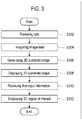
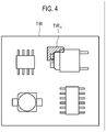
- the region of interest is fixed to a particular shape, for example, a rectangle. Accordingly, when a plurality of regions of interest is set on the image of the substrate, a new region of interest cannot be set by combining a region of interest with the previously set region of interest, and must be set by newly adding a region of interest. Meanwhile, as the shapes of electronic components mounted on the substrate become more diverse, it is necessary to set the region of interest having arbitrary shape on the image of the substrate, and it is also necessary to set a 3D region of interest on a 3D image of the substrate.
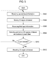
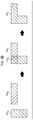
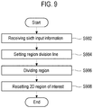
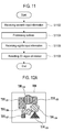
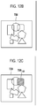
- FIG. 11 is a flowchart illustrating a process of resetting a 2D region of interest by performing outline processing in at least two 2D regions of interest set on the substrate image according to the first embodiment of the present disclosure.
- the 2D substrate image is an image (hereinafter, referred to as a "2D development image") that is two-dimensionally developed from the 3D substrate image.
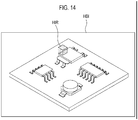
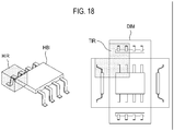
- the processor 130 is configured to generate a 2D development image DIM by two-dimensionally developing a 3D substrate image HBI, as illustrated in FIG. 16 .
- the 2D development image DIM includes 2D images corresponding to the top surface and four lateral surfaces of the 3D substrate image HBI. That is, the 2D development image DIM does not include a 2D image corresponding to the bottom (that is, the surface which cannot be photographed by the substrate photographing part 110) of the 3D substrate image HBI.
- the 2D substrate image generated by the processor 130 is displayed on the display part 140 in S1516.
- the 3D substrate image and the 2D substrate image are displayed on the display part 140 in leftward and rightward directions.
- the 3D substrate image and the 2D substrate image are displayed on the display part 140 in upward and downward directions.
- the substrate photographing part 2110 is configured to radiate a light on a substrate having an inspection object, and receive the light reflected from the substrate so as to acquire image data corresponding to the inspection object in the substrate.
- the image data includes a plurality of view data.
- the substrate inspection system 2100 further includes a user input part 2120.
- the user input part 2120 is configured to receive input information for setting a region of interest with respect to a substrate image corresponding to the substrate S from the user. Further, the user input part 2120 is configured to receive input information for adjusting reference data for a plurality of view data and setting an inspection condition for the region of interest.
- the processor 2130 When input information (hereinafter, referred to as "twelfth input information") for setting a region of interest at a particular position of the 3D substrate image is received through the user input part 2120 in S2310, the processor 2130 is configured to display a 3D region of interest on the display part 2140 in accordance with the twelfth input information in S2312. Since the twelfth input information is the same as the ninth input information in the second embodiment, a detailed description thereof will be omitted in the present embodiment.
Landscapes
- Engineering & Computer Science (AREA)
- Physics & Mathematics (AREA)
- General Physics & Mathematics (AREA)
- Theoretical Computer Science (AREA)
- Computer Vision & Pattern Recognition (AREA)
- Geometry (AREA)
- General Engineering & Computer Science (AREA)
- Microelectronics & Electronic Packaging (AREA)
- Computer Hardware Design (AREA)
- Quality & Reliability (AREA)
- Optics & Photonics (AREA)
- Computer Graphics (AREA)
- Software Systems (AREA)
- Investigating Materials By The Use Of Optical Means Adapted For Particular Applications (AREA)
- Image Processing (AREA)
- Length Measuring Devices By Optical Means (AREA)
- Manufacturing & Machinery (AREA)
- Image Analysis (AREA)
Priority Applications (1)
| Application Number | Priority Date | Filing Date | Title |
|---|---|---|---|
| EP20190465.3A EP3764320B1 (de) | 2015-02-27 | 2016-01-29 | Verfahren und system zur substratinspektion |
Applications Claiming Priority (3)
| Application Number | Priority Date | Filing Date | Title |
|---|---|---|---|
| KR20150028627 | 2015-02-27 | ||
| KR1020160008813A KR101784276B1 (ko) | 2015-02-27 | 2016-01-25 | 기판 검사 방법 및 시스템 |
| PCT/KR2016/000997 WO2016137130A1 (ko) | 2015-02-27 | 2016-01-29 | 기판 검사 방법 및 시스템 |
Related Child Applications (2)
| Application Number | Title | Priority Date | Filing Date |
|---|---|---|---|
| EP20190465.3A Division-Into EP3764320B1 (de) | 2015-02-27 | 2016-01-29 | Verfahren und system zur substratinspektion |
| EP20190465.3A Division EP3764320B1 (de) | 2015-02-27 | 2016-01-29 | Verfahren und system zur substratinspektion |
Publications (3)
| Publication Number | Publication Date |
|---|---|
| EP3264448A1 true EP3264448A1 (de) | 2018-01-03 |
| EP3264448A4 EP3264448A4 (de) | 2018-10-31 |
| EP3264448B1 EP3264448B1 (de) | 2020-09-23 |
Family
ID=56946136
Family Applications (2)
| Application Number | Title | Priority Date | Filing Date |
|---|---|---|---|
| EP16755780.0A Active EP3264448B1 (de) | 2015-02-27 | 2016-01-29 | Verfahren und system zur substratinspektion |
| EP20190465.3A Active EP3764320B1 (de) | 2015-02-27 | 2016-01-29 | Verfahren und system zur substratinspektion |
Family Applications After (1)
| Application Number | Title | Priority Date | Filing Date |
|---|---|---|---|
| EP20190465.3A Active EP3764320B1 (de) | 2015-02-27 | 2016-01-29 | Verfahren und system zur substratinspektion |
Country Status (4)
| Country | Link |
|---|---|
| US (1) | US10672116B2 (de) |
| EP (2) | EP3264448B1 (de) |
| KR (2) | KR101784276B1 (de) |
| CN (1) | CN107408518B (de) |
Families Citing this family (7)
| Publication number | Priority date | Publication date | Assignee | Title |
|---|---|---|---|---|
| KR101784276B1 (ko) * | 2015-02-27 | 2017-10-12 | 주식회사 고영테크놀러지 | 기판 검사 방법 및 시스템 |
| SG11201709029QA (en) * | 2017-05-02 | 2018-12-28 | Generic Power Pte Ltd | System and Method for Lead Foot Angle Inspection Using Multiview Stereo Vision |
| JP6897398B2 (ja) * | 2017-07-31 | 2021-06-30 | セイコーエプソン株式会社 | 三次元形状測定装置、ロボットシステム、及び三次元形状測定方法 |
| KR102211600B1 (ko) * | 2018-10-15 | 2021-02-03 | 주식회사 고영테크놀러지 | 무 초점(Focus-less) 검사 장치 및 검사 방법 |
| EP3640629B1 (de) | 2018-10-15 | 2024-05-08 | Koh Young Technology Inc | Vorrichtung und verfahren zur fokuslosen inspektion |
| CN109752392B (zh) * | 2018-12-24 | 2021-08-03 | 苏州江奥光电科技有限公司 | 一种pcb板缺陷类型检测系统和方法 |
| IT202100001718A1 (it) | 2021-01-28 | 2022-07-28 | Getcoo S R L | Metodo di elaborazione di un'immagine di un oggetto e sistema per l'ispezione dell'oggetto. |
Family Cites Families (26)
| Publication number | Priority date | Publication date | Assignee | Title |
|---|---|---|---|---|
| JPS6361104A (ja) * | 1986-08-30 | 1988-03-17 | T Ii D:Kk | 位置ずれ検査装置 |
| JPH05102275A (ja) | 1991-10-07 | 1993-04-23 | Sony Corp | 欠陥検出方法および欠陥検出装置 |
| JPH06149967A (ja) | 1992-11-16 | 1994-05-31 | Toshiba Medical Eng Co Ltd | 三次元画像診断装置 |
| JPH1047929A (ja) | 1996-07-31 | 1998-02-20 | Seidensha Denshi Kogyo Kk | 筒体の内面検査方法およびその装置 |
| US5966677A (en) | 1997-02-28 | 1999-10-12 | Fiekowsky; Peter J. | High accuracy particle dimension measurement system |
| US6476913B1 (en) * | 1998-11-30 | 2002-11-05 | Hitachi, Ltd. | Inspection method, apparatus and system for circuit pattern |
| WO2001041068A1 (fr) | 1999-11-29 | 2001-06-07 | Olympus Optical Co., Ltd. | Systeme de detection de defaut |
| WO2002001597A1 (en) * | 2000-06-27 | 2002-01-03 | Ebara Corporation | Charged particle beam inspection apparatus and method for fabricating device using that inspection apparatus |
| DE102007047933B3 (de) | 2007-12-20 | 2009-02-26 | Vistec Semiconductor Systems Gmbh | Verfahren zur Inspektion von einer Oberfläche eines Wafers mit Bereichen unterschiedlicher Detektionsempfindlichkeit |
| DE102010064635B4 (de) | 2009-07-03 | 2024-03-14 | Koh Young Technology Inc. | Verfahren zum Untersuchen eines Messobjektes |
| KR101133641B1 (ko) | 2010-01-29 | 2012-04-10 | 주식회사 고영테크놀러지 | 3차원 형상 검사방법 |
| KR101056995B1 (ko) | 2009-07-03 | 2011-08-16 | 주식회사 고영테크놀러지 | 3차원 형상 검사방법 |
| JP5357725B2 (ja) | 2009-12-03 | 2013-12-04 | 株式会社日立ハイテクノロジーズ | 欠陥検査方法及び欠陥検査装置 |
| KR101342203B1 (ko) * | 2010-01-05 | 2013-12-16 | 가부시키가이샤 히다치 하이테크놀로지즈 | Sem을 이용한 결함 검사 방법 및 장치 |
| KR101078781B1 (ko) | 2010-02-01 | 2011-11-01 | 주식회사 고영테크놀러지 | 3차원 형상 검사방법 |
| JP5444092B2 (ja) | 2010-04-06 | 2014-03-19 | 株式会社日立ハイテクノロジーズ | 検査方法およびその装置 |
| JP5599062B2 (ja) * | 2010-12-06 | 2014-10-01 | 株式会社リガク | X線回折装置及びx線回折測定方法 |
| DE112011104658B4 (de) * | 2010-12-29 | 2020-06-18 | Koh Young Technology Inc. | Verfahren zum Prüfen eines Substrats |
| JP5765651B2 (ja) | 2011-02-01 | 2015-08-19 | Jukiオートメーションシステムズ株式会社 | 3次元測定装置 |
| JP5626122B2 (ja) | 2011-05-30 | 2014-11-19 | 東京エレクトロン株式会社 | 基板検査装置、基板検査方法及び記憶媒体 |
| KR20150017421A (ko) | 2013-07-17 | 2015-02-17 | 주식회사 고영테크놀러지 | 3차원 기판검사장치의 그래픽 유저 인터페이스 |
| KR101457040B1 (ko) | 2013-09-03 | 2014-10-31 | 주식회사 고영테크놀러지 | 3차원 기판검사장치의 그래픽 유저 인터페이스 |
| US9494468B2 (en) * | 2013-10-01 | 2016-11-15 | Infineon Technologies Ag | Method of examining a substrate and corresponding device |
| CN103698910B (zh) | 2013-11-28 | 2016-03-16 | 南京中电熊猫液晶显示科技有限公司 | 一种异物检查机及其检查方法 |
| KR101784276B1 (ko) * | 2015-02-27 | 2017-10-12 | 주식회사 고영테크놀러지 | 기판 검사 방법 및 시스템 |
| JP7188870B2 (ja) * | 2017-05-31 | 2022-12-13 | 株式会社キーエンス | 画像検査装置 |
-
2016
- 2016-01-25 KR KR1020160008813A patent/KR101784276B1/ko active Active
- 2016-01-29 CN CN201680012305.1A patent/CN107408518B/zh active Active
- 2016-01-29 EP EP16755780.0A patent/EP3264448B1/de active Active
- 2016-01-29 EP EP20190465.3A patent/EP3764320B1/de active Active
- 2016-01-29 US US15/554,041 patent/US10672116B2/en active Active
-
2017
- 2017-02-13 KR KR1020170019505A patent/KR101810992B1/ko active Active
Also Published As
| Publication number | Publication date |
|---|---|
| EP3764320C0 (de) | 2023-07-19 |
| KR101784276B1 (ko) | 2017-10-12 |
| EP3264448B1 (de) | 2020-09-23 |
| EP3764320A1 (de) | 2021-01-13 |
| KR20160105295A (ko) | 2016-09-06 |
| US10672116B2 (en) | 2020-06-02 |
| KR20170019403A (ko) | 2017-02-21 |
| EP3764320B1 (de) | 2023-07-19 |
| US20180040118A1 (en) | 2018-02-08 |
| KR101810992B1 (ko) | 2017-12-20 |
| CN107408518B (zh) | 2021-01-05 |
| EP3264448A4 (de) | 2018-10-31 |
| CN107408518A (zh) | 2017-11-28 |
Similar Documents
| Publication | Publication Date | Title |
|---|---|---|
| EP3764320B1 (de) | Verfahren und system zur substratinspektion | |
| KR102461093B1 (ko) | 깊이 영상 제공 장치 및 방법 | |
| JP6364777B2 (ja) | 画像データ取得システム及び画像データ取得方法 | |
| EP3382645B1 (de) | Verfahren zur erzeugung eines 3d-modells auf basis von structure from motion und photometrischem stereo von sparse 2d bildern | |
| JP6104662B2 (ja) | 計測装置、方法及びプログラム | |
| CN108616726A (zh) | 基于结构光的曝光控制方法及曝光控制装置 | |
| CN111344103B (zh) | 基于高光谱光学传感器的涂层区域定位方法和装置、及除胶系统 | |
| JP6211197B2 (ja) | 基板検査装置 | |
| JP6425406B2 (ja) | 情報処理装置、情報処理方法、プログラム | |
| JP6792369B2 (ja) | 回路基板の検査方法及び検査装置 | |
| US10986761B2 (en) | Board inspecting apparatus and board inspecting method using the same | |
| JP2017122614A (ja) | 画像生成方法及び検査装置 | |
| JP5611875B2 (ja) | 情報表示装置、情報表示方法、及びプログラム | |
| US20160027183A1 (en) | Image processing apparatus, image processing method and program | |
| US11062184B1 (en) | Using augmented reality to perform complex print jobs | |
| CN109804730B (zh) | 基板检查装置及利用其的基板歪曲补偿方法 | |
| CN108777784B (zh) | 深度获取方法和装置、电子装置、计算机设备和存储介质 | |
| JP6229134B2 (ja) | 計測装置 | |
| WO2011096136A1 (ja) | 疑似画像生成装置および疑似画像生成方法 | |
| EP4269940B1 (de) | Vorrichtung und verfahren zur inspektion | |
| KR101511089B1 (ko) | Aoi 장비의 티칭 데이터 자동 생성 방법 | |
| JP7156794B2 (ja) | 検査装置の高さ情報の取得方法及び検査装置 | |
| US10360719B2 (en) | Method and apparatus for obtaining high-quality textures | |
| JP2023030314A (ja) | 三次元計測装置、及び、三次元計測における高さ計測の計測誤差を決定する方法 | |
| JP2022147530A (ja) | 特徴位置推定方法、特徴位置推定装置、及び、特徴位置推定プログラム |
Legal Events
| Date | Code | Title | Description |
|---|---|---|---|
| STAA | Information on the status of an ep patent application or granted ep patent |
Free format text: STATUS: THE INTERNATIONAL PUBLICATION HAS BEEN MADE |
|
| PUAI | Public reference made under article 153(3) epc to a published international application that has entered the european phase |
Free format text: ORIGINAL CODE: 0009012 |
|
| STAA | Information on the status of an ep patent application or granted ep patent |
Free format text: STATUS: REQUEST FOR EXAMINATION WAS MADE |
|
| 17P | Request for examination filed |
Effective date: 20170911 |
|
| AK | Designated contracting states |
Kind code of ref document: A1 Designated state(s): AL AT BE BG CH CY CZ DE DK EE ES FI FR GB GR HR HU IE IS IT LI LT LU LV MC MK MT NL NO PL PT RO RS SE SI SK SM TR |
|
| AX | Request for extension of the european patent |
Extension state: BA ME |
|
| DAV | Request for validation of the european patent (deleted) | ||
| DAX | Request for extension of the european patent (deleted) | ||
| A4 | Supplementary search report drawn up and despatched |
Effective date: 20181001 |
|
| RIC1 | Information provided on ipc code assigned before grant |
Ipc: G06T 7/00 20170101AFI20180925BHEP Ipc: G06T 7/62 20170101ALI20180925BHEP |
|
| STAA | Information on the status of an ep patent application or granted ep patent |
Free format text: STATUS: EXAMINATION IS IN PROGRESS |
|
| 17Q | First examination report despatched |
Effective date: 20191031 |
|
| REG | Reference to a national code |
Ref country code: DE Ref legal event code: R079 Ref document number: 602016044547 Country of ref document: DE Free format text: PREVIOUS MAIN CLASS: H01L0021660000 Ipc: G06T0007000000 |
|
| GRAP | Despatch of communication of intention to grant a patent |
Free format text: ORIGINAL CODE: EPIDOSNIGR1 |
|
| RIC1 | Information provided on ipc code assigned before grant |
Ipc: G06T 7/00 20170101AFI20200312BHEP Ipc: G01N 21/956 20060101ALI20200312BHEP Ipc: G06T 7/62 20170101ALI20200312BHEP |
|
| STAA | Information on the status of an ep patent application or granted ep patent |
Free format text: STATUS: GRANT OF PATENT IS INTENDED |
|
| INTG | Intention to grant announced |
Effective date: 20200416 |
|
| GRAS | Grant fee paid |
Free format text: ORIGINAL CODE: EPIDOSNIGR3 |
|
| GRAA | (expected) grant |
Free format text: ORIGINAL CODE: 0009210 |
|
| STAA | Information on the status of an ep patent application or granted ep patent |
Free format text: STATUS: THE PATENT HAS BEEN GRANTED |
|
| AK | Designated contracting states |
Kind code of ref document: B1 Designated state(s): AL AT BE BG CH CY CZ DE DK EE ES FI FR GB GR HR HU IE IS IT LI LT LU LV MC MK MT NL NO PL PT RO RS SE SI SK SM TR |
|
| REG | Reference to a national code |
Ref country code: GB Ref legal event code: FG4D |
|
| REG | Reference to a national code |
Ref country code: CH Ref legal event code: EP |
|
| REG | Reference to a national code |
Ref country code: IE Ref legal event code: FG4D |
|
| REG | Reference to a national code |
Ref country code: AT Ref legal event code: REF Ref document number: 1317150 Country of ref document: AT Kind code of ref document: T Effective date: 20201015 Ref country code: DE Ref legal event code: R096 Ref document number: 602016044547 Country of ref document: DE |
|
| PG25 | Lapsed in a contracting state [announced via postgrant information from national office to epo] |
Ref country code: HR Free format text: LAPSE BECAUSE OF FAILURE TO SUBMIT A TRANSLATION OF THE DESCRIPTION OR TO PAY THE FEE WITHIN THE PRESCRIBED TIME-LIMIT Effective date: 20200923 Ref country code: GR Free format text: LAPSE BECAUSE OF FAILURE TO SUBMIT A TRANSLATION OF THE DESCRIPTION OR TO PAY THE FEE WITHIN THE PRESCRIBED TIME-LIMIT Effective date: 20201224 Ref country code: NO Free format text: LAPSE BECAUSE OF FAILURE TO SUBMIT A TRANSLATION OF THE DESCRIPTION OR TO PAY THE FEE WITHIN THE PRESCRIBED TIME-LIMIT Effective date: 20201223 Ref country code: BG Free format text: LAPSE BECAUSE OF FAILURE TO SUBMIT A TRANSLATION OF THE DESCRIPTION OR TO PAY THE FEE WITHIN THE PRESCRIBED TIME-LIMIT Effective date: 20201223 Ref country code: SE Free format text: LAPSE BECAUSE OF FAILURE TO SUBMIT A TRANSLATION OF THE DESCRIPTION OR TO PAY THE FEE WITHIN THE PRESCRIBED TIME-LIMIT Effective date: 20200923 Ref country code: FI Free format text: LAPSE BECAUSE OF FAILURE TO SUBMIT A TRANSLATION OF THE DESCRIPTION OR TO PAY THE FEE WITHIN THE PRESCRIBED TIME-LIMIT Effective date: 20200923 |
|
| REG | Reference to a national code |
Ref country code: AT Ref legal event code: MK05 Ref document number: 1317150 Country of ref document: AT Kind code of ref document: T Effective date: 20200923 |
|
| PG25 | Lapsed in a contracting state [announced via postgrant information from national office to epo] |
Ref country code: LV Free format text: LAPSE BECAUSE OF FAILURE TO SUBMIT A TRANSLATION OF THE DESCRIPTION OR TO PAY THE FEE WITHIN THE PRESCRIBED TIME-LIMIT Effective date: 20200923 Ref country code: RS Free format text: LAPSE BECAUSE OF FAILURE TO SUBMIT A TRANSLATION OF THE DESCRIPTION OR TO PAY THE FEE WITHIN THE PRESCRIBED TIME-LIMIT Effective date: 20200923 |
|
| REG | Reference to a national code |
Ref country code: NL Ref legal event code: MP Effective date: 20200923 |
|
| REG | Reference to a national code |
Ref country code: LT Ref legal event code: MG4D |
|
| PG25 | Lapsed in a contracting state [announced via postgrant information from national office to epo] |
Ref country code: PT Free format text: LAPSE BECAUSE OF FAILURE TO SUBMIT A TRANSLATION OF THE DESCRIPTION OR TO PAY THE FEE WITHIN THE PRESCRIBED TIME-LIMIT Effective date: 20210125 Ref country code: RO Free format text: LAPSE BECAUSE OF FAILURE TO SUBMIT A TRANSLATION OF THE DESCRIPTION OR TO PAY THE FEE WITHIN THE PRESCRIBED TIME-LIMIT Effective date: 20200923 Ref country code: CZ Free format text: LAPSE BECAUSE OF FAILURE TO SUBMIT A TRANSLATION OF THE DESCRIPTION OR TO PAY THE FEE WITHIN THE PRESCRIBED TIME-LIMIT Effective date: 20200923 Ref country code: LT Free format text: LAPSE BECAUSE OF FAILURE TO SUBMIT A TRANSLATION OF THE DESCRIPTION OR TO PAY THE FEE WITHIN THE PRESCRIBED TIME-LIMIT Effective date: 20200923 Ref country code: EE Free format text: LAPSE BECAUSE OF FAILURE TO SUBMIT A TRANSLATION OF THE DESCRIPTION OR TO PAY THE FEE WITHIN THE PRESCRIBED TIME-LIMIT Effective date: 20200923 Ref country code: SM Free format text: LAPSE BECAUSE OF FAILURE TO SUBMIT A TRANSLATION OF THE DESCRIPTION OR TO PAY THE FEE WITHIN THE PRESCRIBED TIME-LIMIT Effective date: 20200923 |
|
| PG25 | Lapsed in a contracting state [announced via postgrant information from national office to epo] |
Ref country code: ES Free format text: LAPSE BECAUSE OF FAILURE TO SUBMIT A TRANSLATION OF THE DESCRIPTION OR TO PAY THE FEE WITHIN THE PRESCRIBED TIME-LIMIT Effective date: 20200923 Ref country code: AT Free format text: LAPSE BECAUSE OF FAILURE TO SUBMIT A TRANSLATION OF THE DESCRIPTION OR TO PAY THE FEE WITHIN THE PRESCRIBED TIME-LIMIT Effective date: 20200923 Ref country code: AL Free format text: LAPSE BECAUSE OF FAILURE TO SUBMIT A TRANSLATION OF THE DESCRIPTION OR TO PAY THE FEE WITHIN THE PRESCRIBED TIME-LIMIT Effective date: 20200923 Ref country code: IS Free format text: LAPSE BECAUSE OF FAILURE TO SUBMIT A TRANSLATION OF THE DESCRIPTION OR TO PAY THE FEE WITHIN THE PRESCRIBED TIME-LIMIT Effective date: 20210123 Ref country code: PL Free format text: LAPSE BECAUSE OF FAILURE TO SUBMIT A TRANSLATION OF THE DESCRIPTION OR TO PAY THE FEE WITHIN THE PRESCRIBED TIME-LIMIT Effective date: 20200923 |
|
| REG | Reference to a national code |
Ref country code: DE Ref legal event code: R097 Ref document number: 602016044547 Country of ref document: DE |
|
| PG25 | Lapsed in a contracting state [announced via postgrant information from national office to epo] |
Ref country code: SK Free format text: LAPSE BECAUSE OF FAILURE TO SUBMIT A TRANSLATION OF THE DESCRIPTION OR TO PAY THE FEE WITHIN THE PRESCRIBED TIME-LIMIT Effective date: 20200923 |
|
| PLBE | No opposition filed within time limit |
Free format text: ORIGINAL CODE: 0009261 |
|
| STAA | Information on the status of an ep patent application or granted ep patent |
Free format text: STATUS: NO OPPOSITION FILED WITHIN TIME LIMIT |
|
| PG25 | Lapsed in a contracting state [announced via postgrant information from national office to epo] |
Ref country code: SI Free format text: LAPSE BECAUSE OF FAILURE TO SUBMIT A TRANSLATION OF THE DESCRIPTION OR TO PAY THE FEE WITHIN THE PRESCRIBED TIME-LIMIT Effective date: 20200923 Ref country code: MC Free format text: LAPSE BECAUSE OF FAILURE TO SUBMIT A TRANSLATION OF THE DESCRIPTION OR TO PAY THE FEE WITHIN THE PRESCRIBED TIME-LIMIT Effective date: 20200923 Ref country code: DK Free format text: LAPSE BECAUSE OF FAILURE TO SUBMIT A TRANSLATION OF THE DESCRIPTION OR TO PAY THE FEE WITHIN THE PRESCRIBED TIME-LIMIT Effective date: 20200923 |
|
| REG | Reference to a national code |
Ref country code: CH Ref legal event code: PL |
|
| 26N | No opposition filed |
Effective date: 20210624 |
|
| GBPC | Gb: european patent ceased through non-payment of renewal fee |
Effective date: 20210129 |
|
| PG25 | Lapsed in a contracting state [announced via postgrant information from national office to epo] |
Ref country code: LU Free format text: LAPSE BECAUSE OF NON-PAYMENT OF DUE FEES Effective date: 20210129 |
|
| REG | Reference to a national code |
Ref country code: BE Ref legal event code: MM Effective date: 20210131 |
|
| PG25 | Lapsed in a contracting state [announced via postgrant information from national office to epo] |
Ref country code: IT Free format text: LAPSE BECAUSE OF FAILURE TO SUBMIT A TRANSLATION OF THE DESCRIPTION OR TO PAY THE FEE WITHIN THE PRESCRIBED TIME-LIMIT Effective date: 20200923 Ref country code: FR Free format text: LAPSE BECAUSE OF NON-PAYMENT OF DUE FEES Effective date: 20210131 |
|
| PG25 | Lapsed in a contracting state [announced via postgrant information from national office to epo] |
Ref country code: LI Free format text: LAPSE BECAUSE OF NON-PAYMENT OF DUE FEES Effective date: 20210131 Ref country code: GB Free format text: LAPSE BECAUSE OF NON-PAYMENT OF DUE FEES Effective date: 20210129 Ref country code: CH Free format text: LAPSE BECAUSE OF NON-PAYMENT OF DUE FEES Effective date: 20210131 |
|
| PG25 | Lapsed in a contracting state [announced via postgrant information from national office to epo] |
Ref country code: IE Free format text: LAPSE BECAUSE OF NON-PAYMENT OF DUE FEES Effective date: 20210129 |
|
| PG25 | Lapsed in a contracting state [announced via postgrant information from national office to epo] |
Ref country code: IS Free format text: LAPSE BECAUSE OF FAILURE TO SUBMIT A TRANSLATION OF THE DESCRIPTION OR TO PAY THE FEE WITHIN THE PRESCRIBED TIME-LIMIT Effective date: 20210123 |
|
| PG25 | Lapsed in a contracting state [announced via postgrant information from national office to epo] |
Ref country code: BE Free format text: LAPSE BECAUSE OF NON-PAYMENT OF DUE FEES Effective date: 20210131 |
|
| PG25 | Lapsed in a contracting state [announced via postgrant information from national office to epo] |
Ref country code: NL Free format text: LAPSE BECAUSE OF NON-PAYMENT OF DUE FEES Effective date: 20200923 Ref country code: CY Free format text: LAPSE BECAUSE OF FAILURE TO SUBMIT A TRANSLATION OF THE DESCRIPTION OR TO PAY THE FEE WITHIN THE PRESCRIBED TIME-LIMIT Effective date: 20200923 |
|
| PG25 | Lapsed in a contracting state [announced via postgrant information from national office to epo] |
Ref country code: HU Free format text: LAPSE BECAUSE OF FAILURE TO SUBMIT A TRANSLATION OF THE DESCRIPTION OR TO PAY THE FEE WITHIN THE PRESCRIBED TIME-LIMIT; INVALID AB INITIO Effective date: 20160129 |
|
| PG25 | Lapsed in a contracting state [announced via postgrant information from national office to epo] |
Ref country code: MK Free format text: LAPSE BECAUSE OF FAILURE TO SUBMIT A TRANSLATION OF THE DESCRIPTION OR TO PAY THE FEE WITHIN THE PRESCRIBED TIME-LIMIT Effective date: 20200923 |
|
| PG25 | Lapsed in a contracting state [announced via postgrant information from national office to epo] |
Ref country code: MT Free format text: LAPSE BECAUSE OF FAILURE TO SUBMIT A TRANSLATION OF THE DESCRIPTION OR TO PAY THE FEE WITHIN THE PRESCRIBED TIME-LIMIT Effective date: 20200923 |
|
| PG25 | Lapsed in a contracting state [announced via postgrant information from national office to epo] |
Ref country code: TR Free format text: LAPSE BECAUSE OF FAILURE TO SUBMIT A TRANSLATION OF THE DESCRIPTION OR TO PAY THE FEE WITHIN THE PRESCRIBED TIME-LIMIT Effective date: 20200923 |
|
| PGFP | Annual fee paid to national office [announced via postgrant information from national office to epo] |
Ref country code: DE Payment date: 20251203 Year of fee payment: 11 |