EP3259227B1 - Selektive gestufte beschichtung für mikrogefertigte strukturen - Google Patents
Selektive gestufte beschichtung für mikrogefertigte strukturen Download PDFInfo
- Publication number
- EP3259227B1 EP3259227B1 EP16709197.4A EP16709197A EP3259227B1 EP 3259227 B1 EP3259227 B1 EP 3259227B1 EP 16709197 A EP16709197 A EP 16709197A EP 3259227 B1 EP3259227 B1 EP 3259227B1
- Authority
- EP
- European Patent Office
- Prior art keywords
- opening
- shadow mask
- thickness
- width
- micro
- Prior art date
- Legal status (The legal status is an assumption and is not a legal conclusion. Google has not performed a legal analysis and makes no representation as to the accuracy of the status listed.)
- Active
Links
Images


Classifications
-
- B—PERFORMING OPERATIONS; TRANSPORTING
- B05—SPRAYING OR ATOMISING IN GENERAL; APPLYING FLUENT MATERIALS TO SURFACES, IN GENERAL
- B05B—SPRAYING APPARATUS; ATOMISING APPARATUS; NOZZLES
- B05B12/00—Arrangements for controlling delivery; Arrangements for controlling the spray area
- B05B12/16—Arrangements for controlling delivery; Arrangements for controlling the spray area for controlling the spray area
- B05B12/20—Masking elements, i.e. elements defining uncoated areas on an object to be coated
-
- B—PERFORMING OPERATIONS; TRANSPORTING
- B81—MICROSTRUCTURAL TECHNOLOGY
- B81C—PROCESSES OR APPARATUS SPECIALLY ADAPTED FOR THE MANUFACTURE OR TREATMENT OF MICROSTRUCTURAL DEVICES OR SYSTEMS
- B81C1/00—Manufacture or treatment of devices or systems in or on a substrate
- B81C1/00349—Creating layers of material on a substrate
- B81C1/00373—Selective deposition, e.g. printing or microcontact printing
-
- B—PERFORMING OPERATIONS; TRANSPORTING
- B81—MICROSTRUCTURAL TECHNOLOGY
- B81C—PROCESSES OR APPARATUS SPECIALLY ADAPTED FOR THE MANUFACTURE OR TREATMENT OF MICROSTRUCTURAL DEVICES OR SYSTEMS
- B81C1/00—Manufacture or treatment of devices or systems in or on a substrate
- B81C1/00349—Creating layers of material on a substrate
- B81C1/0038—Processes for creating layers of materials not provided for in groups B81C1/00357 - B81C1/00373
-
- B—PERFORMING OPERATIONS; TRANSPORTING
- B81—MICROSTRUCTURAL TECHNOLOGY
- B81C—PROCESSES OR APPARATUS SPECIALLY ADAPTED FOR THE MANUFACTURE OR TREATMENT OF MICROSTRUCTURAL DEVICES OR SYSTEMS
- B81C1/00—Manufacture or treatment of devices or systems in or on a substrate
- B81C1/00388—Etch mask forming
- B81C1/00404—Mask characterised by its size, orientation or shape
-
- C—CHEMISTRY; METALLURGY
- C23—COATING METALLIC MATERIAL; COATING MATERIAL WITH METALLIC MATERIAL; CHEMICAL SURFACE TREATMENT; DIFFUSION TREATMENT OF METALLIC MATERIAL; COATING BY VACUUM EVAPORATION, BY SPUTTERING, BY ION IMPLANTATION OR BY CHEMICAL VAPOUR DEPOSITION, IN GENERAL; INHIBITING CORROSION OF METALLIC MATERIAL OR INCRUSTATION IN GENERAL
- C23C—COATING METALLIC MATERIAL; COATING MATERIAL WITH METALLIC MATERIAL; SURFACE TREATMENT OF METALLIC MATERIAL BY DIFFUSION INTO THE SURFACE, BY CHEMICAL CONVERSION OR SUBSTITUTION; COATING BY VACUUM EVAPORATION, BY SPUTTERING, BY ION IMPLANTATION OR BY CHEMICAL VAPOUR DEPOSITION, IN GENERAL
- C23C14/00—Coating by vacuum evaporation, by sputtering or by ion implantation of the coating forming material
- C23C14/04—Coating on selected surface areas, e.g. using masks
- C23C14/042—Coating on selected surface areas, e.g. using masks using masks
-
- C—CHEMISTRY; METALLURGY
- C23—COATING METALLIC MATERIAL; COATING MATERIAL WITH METALLIC MATERIAL; CHEMICAL SURFACE TREATMENT; DIFFUSION TREATMENT OF METALLIC MATERIAL; COATING BY VACUUM EVAPORATION, BY SPUTTERING, BY ION IMPLANTATION OR BY CHEMICAL VAPOUR DEPOSITION, IN GENERAL; INHIBITING CORROSION OF METALLIC MATERIAL OR INCRUSTATION IN GENERAL
- C23C—COATING METALLIC MATERIAL; COATING MATERIAL WITH METALLIC MATERIAL; SURFACE TREATMENT OF METALLIC MATERIAL BY DIFFUSION INTO THE SURFACE, BY CHEMICAL CONVERSION OR SUBSTITUTION; COATING BY VACUUM EVAPORATION, BY SPUTTERING, BY ION IMPLANTATION OR BY CHEMICAL VAPOUR DEPOSITION, IN GENERAL
- C23C14/00—Coating by vacuum evaporation, by sputtering or by ion implantation of the coating forming material
- C23C14/04—Coating on selected surface areas, e.g. using masks
- C23C14/046—Coating cavities or hollow spaces, e.g. interior of tubes; Infiltration of porous substrates
-
- C—CHEMISTRY; METALLURGY
- C23—COATING METALLIC MATERIAL; COATING MATERIAL WITH METALLIC MATERIAL; CHEMICAL SURFACE TREATMENT; DIFFUSION TREATMENT OF METALLIC MATERIAL; COATING BY VACUUM EVAPORATION, BY SPUTTERING, BY ION IMPLANTATION OR BY CHEMICAL VAPOUR DEPOSITION, IN GENERAL; INHIBITING CORROSION OF METALLIC MATERIAL OR INCRUSTATION IN GENERAL
- C23C—COATING METALLIC MATERIAL; COATING MATERIAL WITH METALLIC MATERIAL; SURFACE TREATMENT OF METALLIC MATERIAL BY DIFFUSION INTO THE SURFACE, BY CHEMICAL CONVERSION OR SUBSTITUTION; COATING BY VACUUM EVAPORATION, BY SPUTTERING, BY ION IMPLANTATION OR BY CHEMICAL VAPOUR DEPOSITION, IN GENERAL
- C23C16/00—Chemical coating by decomposition of gaseous compounds, without leaving reaction products of surface material in the coating, i.e. chemical vapour deposition [CVD] processes
- C23C16/04—Coating on selected surface areas, e.g. using masks
- C23C16/042—Coating on selected surface areas, e.g. using masks using masks
-
- H—ELECTRICITY
- H01—ELECTRIC ELEMENTS
- H01L—SEMICONDUCTOR DEVICES NOT COVERED BY CLASS H10
- H01L21/00—Processes or apparatus adapted for the manufacture or treatment of semiconductor or solid state devices or of parts thereof
- H01L21/67—Apparatus specially adapted for handling semiconductor or electric solid state devices during manufacture or treatment thereof; Apparatus specially adapted for handling wafers during manufacture or treatment of semiconductor or electric solid state devices or components ; Apparatus not specifically provided for elsewhere
- H01L21/68—Apparatus specially adapted for handling semiconductor or electric solid state devices during manufacture or treatment thereof; Apparatus specially adapted for handling wafers during manufacture or treatment of semiconductor or electric solid state devices or components ; Apparatus not specifically provided for elsewhere for positioning, orientation or alignment
- H01L21/682—Mask-wafer alignment
-
- B—PERFORMING OPERATIONS; TRANSPORTING
- B81—MICROSTRUCTURAL TECHNOLOGY
- B81B—MICROSTRUCTURAL DEVICES OR SYSTEMS, e.g. MICROMECHANICAL DEVICES
- B81B2201/00—Specific applications of microelectromechanical systems
- B81B2201/04—Optical MEMS
- B81B2201/042—Micromirrors, not used as optical switches
-
- B—PERFORMING OPERATIONS; TRANSPORTING
- B81—MICROSTRUCTURAL TECHNOLOGY
- B81B—MICROSTRUCTURAL DEVICES OR SYSTEMS, e.g. MICROMECHANICAL DEVICES
- B81B2201/00—Specific applications of microelectromechanical systems
- B81B2201/04—Optical MEMS
- B81B2201/047—Optical MEMS not provided for in B81B2201/042 - B81B2201/045
-
- B—PERFORMING OPERATIONS; TRANSPORTING
- B81—MICROSTRUCTURAL TECHNOLOGY
- B81C—PROCESSES OR APPARATUS SPECIALLY ADAPTED FOR THE MANUFACTURE OR TREATMENT OF MICROSTRUCTURAL DEVICES OR SYSTEMS
- B81C2201/00—Manufacture or treatment of microstructural devices or systems
- B81C2201/01—Manufacture or treatment of microstructural devices or systems in or on a substrate
- B81C2201/0174—Manufacture or treatment of microstructural devices or systems in or on a substrate for making multi-layered devices, film deposition or growing
- B81C2201/0183—Selective deposition
-
- B—PERFORMING OPERATIONS; TRANSPORTING
- B81—MICROSTRUCTURAL TECHNOLOGY
- B81C—PROCESSES OR APPARATUS SPECIALLY ADAPTED FOR THE MANUFACTURE OR TREATMENT OF MICROSTRUCTURAL DEVICES OR SYSTEMS
- B81C2201/00—Manufacture or treatment of microstructural devices or systems
- B81C2201/01—Manufacture or treatment of microstructural devices or systems in or on a substrate
- B81C2201/0198—Manufacture or treatment of microstructural devices or systems in or on a substrate for making a masking layer
-
- H—ELECTRICITY
- H01—ELECTRIC ELEMENTS
- H01J—ELECTRIC DISCHARGE TUBES OR DISCHARGE LAMPS
- H01J2229/00—Details of cathode ray tubes or electron beam tubes
- H01J2229/07—Shadow masks
Definitions
- the present invention relates in general to metallization or thin film coating of optical surfaces in micro-optical bench devices, and in particular to the fabrication of a shadow mask providing selective step coverage of optical surfaces of micro-fabricated structures within micro-optical bench devices.
- Deeply etched micro-optical benches are typically formed using a Deep Reactive Ion Etching (DRIE) process on Silicon On Insulator (SOI) wafers in order to produce microoptical and Micro-Electro-Mechanical Systems (MEMS) components that are able to process free-space optical beams propagating parallel to the SOI substrate.
- DRIE Deep Reactive Ion Etching
- SOI Silicon On Insulator
- MEMS Micro-Electro-Mechanical Systems
- a one-level shadow mask is used to provide step coverage and selective metallization or thin film coating of optical surfaces within deeply etched micro-optical benches.
- Example of in-plane surfaces coating is described in documents US 2011/0177637 A1 and US 2013/0299345 A1 .
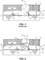
- FIG. 1 illustrates an exemplary prior art one-level shadow mask 100 for use in metallizing etched surfaces of a substrate 110, such as a Silicon On Insulator (SOI) wafer/substrate.
- the substrate 110 includes a device layer 120, an etch stop or sacrificial (e.g., buried oxide (BOX)) layer 130 and a handle layer 140.
- Various micro-fabricated structures e.g., structures 152 and 162 of a micro-optical bench device 170 are etched into the device layer 120 using, for example, a DRIE Bosch process, to expose micro-optical surfaces 150 and 160.
- an opening in the shadow mask of width L m is required, assuming a metallization angle, ⁇ m .
- a protection distance L p from the metallization opening is required.
- L t M + h + D 2 tan ⁇ m h + D 2 D 1 ⁇ h 2 D 2 + 2 h + D 2 tan ⁇ m
- Various aspects of the present disclosure provide a shadow mask for use in selectively coating micro-fabricated structures within a micro-optical bench device.
- the shadow mask includes a first opening within a top surface of the shadow mask and a second opening within a bottom surface of the shadow mask.
- the second opening is aligned with the first opening and has a second width less than a first width of the first opening.
- An overlap between the first opening and the second opening forms a hole within the shadow mask through which selective coating of micro-fabricated structures within the micro-optical bench device may occur.
- the present invention is directed to a method and a shadow mask for selective coating of out-of-plane surfaces of micro-fabricated structures within a device, the main and subsidiaries aspects of which are defined by the appended claims.
- Embodiments and examples in the following description which are not covered by the appended claims are considered as being not part of the present invention, and are merely provided for the purpose of understanding.
- selective metallization or thin film coating of optical surfaces of micro-fabricated structures within micro-optical bench devices is performed using two or more levels of openings in a shadow mask, placed above the micro-optical bench device.
- the multi-level shadow mask enables forming optical mirrors in Silicon-On-Insulator SOI wafers with smaller bench foot print (i.e., reduced optical propagation distance) and controlled thin firm coating of the micro-optical components inside the micro-optical bench device.
- the size and shape of the top level shadow mask openings are used to control the profile and thickness of the deposited thin film.
- the second level shadow mask openings are used to control the spread of the deposition and to protect the surfaces that are not to be coated.
- the multi-level shadow mask may further improve the uniformity of coating from one optical surface to another inside a single micro-optical bench device and across a wafer containing multiple micro-optical bench devices before singulation of the wafer.
- FIG. 2 illustrates an exemplary multi-level shadow mask 200 for use in providing selective step coverage for micro-fabricated structures within a micro-optical bench device 270, in accordance with aspects of the present disclosure.
- the micro-optical bench device 270 is fabricated within a substrate 230, such as a Silicon On Insulator (SOI) wafer/substrate.
- the substrate 230 includes a device layer 240, an etch stop or sacrificial (e.g., buried oxide (BOX)) layer 250 and a handle layer 260.
- SOI Silicon On Insulator
- BOX buried oxide
- micro-fabricated structures e.g., structures 282 and 292 of the micro-optical bench device 270 are etched into the device layer 240 using, for example, a DRIE Bosch process, to expose optical surfaces 280 and 290 thereof.
- the etched optical surfaces 280 and 290 are out-of-plane with respect to the substrate 230 and may be vertical or at an inclination angle with respect to the plane of the substrate 230
- the shadow mask 200 may be, for example, formed of a silicon (Si) substrate or other type of substrate (e.g., plastic, glass, etc.) that has a top surface 202 and a bottom surface 206.
- the multiple levels of the shadow mask 200 are formed using two or more openings therein.
- the shadow mask 200 includes a first opening 205 within the top surface 202 of the shadow mask 200 and a second opening 210 within the bottom surface 204 of the shadow mask 200.
- the second opening 210 is aligned with the first opening 205 and has a width L mb that is less than the width L m of the first opening 205.
- the overlap between the widths of the first and second openings 205 and 210 forms a hole 215 within the shadow mask 200 that extends through the top and bottom surfaces 202 and 204 thereof.
- additional openings between the first and second openings 205 and 210 may also be included within the shadow mask.
- a recessed portion 206 of the shadow mask 200 provides a gap between the shadow mask 200 and the moving/fragile micro-fabricated structures 282 and 292 within the micro-optical bench device 270.
- a protection lip 220 may be formed within the shadow mask 200, in which the width of the protection lip 220 corresponds to a difference between the first width L m of the first opening 205 and the second width L mb of the second opening 210.
- the protection lip 220 enables protection of a surface 290 during deposition of the coating material (i.e., metal layer) on an opposing surface 280.
- the first level D 1 of the shadow mask 200 includes the thickness of the shadow mask 200 less the recessed portion 206 and corresponds to the depth of the hole 215.
- the second level D 2 of the shadow mask 200 includes the total thickness of the shadow mask 200 including the recessed portion 206.
- the third level D 3 of the shadow mask 200 includes the thickness of the shadow mask 200 corresponding to the depth of the second opening 210, in which D 3 is much smaller than D 2 .
- the third level D 3 of the shadow mask 200 extends from the recessed bottom surface 204 of the shadow mask 200 through the depth of the second opening 210.
- the first opening 205 extends from the top surface 202 of the shadow mask 200 through a thickness corresponding to a difference between D 1 and D 3 .
- the protection lip 220 is formed within the third level D 3 of the shadow mask 200.
- the different levels are designed to expose some optical surfaces (e.g., surface 280), while at the same time protect other optical surfaces (e.g, surface 290) within the micro-optical bench device 270.
- these levels represent the control parameters for selective metallization or thin film coating of the micro-optical bench device 270.
- optimization of the levels may further control the optical quality of the micro-mirrors and optical interfaces within the micro-optical bench device 170. Consequently, the multi-level shadow mask 200 enhances the optical efficiency of the micro-optical bench device 170.
- the distance between a surface to be metallized/coated (e.g., surface 280) and a surface to be protected from metallization/thin film coating (e.g., surface 390) may be minimized by controlling the shadow mask levels.
- the width of the top level opening 205 may be the same as that shown in FIG. 1 , and thus, given by Equation 1.
- the total optical propagation distance ( L t ) may be reduced to half of the value when using the conventional shadow mask. Further reduction may also be achieved by further increases in D 2 and/or decreases in D 3 .
- the sputtered metal thickness profile and maximum thickness value may be controlled by the shadow mask opening shape and profile, respectively, as shown in FIG. 3 .
- the shape of the shadow mask top opening g(x,y) controls the profile shape of the sputtered thin film t(x,y).
- the maximum achievable thickness is controlled from t 1 to t 2 ... to t 4 , as shown in FIG. 4 .
- the opening size is smaller than a given threshold value L m-th , the sputtering thickness will be negligible. This threshold value is controlled by the process conditions, including the distance between the target and the wafer in the reactor, biasing power and the sputtering gas.
- the threshold value depends on the overall thickness of the shadow mask used.
- An example experimental dependence of the thin firm thickness on the opening size is shown in FIG. 5 .
- the thickness saturates a certain value. This value is controlled by the process time and process conditions.
- the shadow mask 200 may have different opening sizes simultaneously leading to different metallization or thin film thickness. This may enable, for example, the formation of fully reflective mirrors 282b and partially reflective/transmitting mirrors 280a with controlled transmission.
- the different top level opening sizes lead to two different thin film thicknesses t 1 and t 2 on the coated optical surfaces 280a and 280b of micro-fabricated structures 282a and 282b.
- the coated surfaces 280a and 280b may have different reflectivity and transmission characteristics, depending on the metal thickness with respect to the optical skin depth at the given wavelength of the light propagating in the micro-optical bench 270. If one or both of the metallized surfaces 280a and 280b coating thickness is much larger than the skin depth, then the surface (e.g., surface 280b) will act as a fully reflecting surface with the respect to the incident light.
- the widths of the bottom level openings 210a and 210b may be the same or different.
- the widths of the bottom level openings 210a and 210b may be selected to provide protection to other surfaces 290a and 290b within the micro-optical bench device 270 during deposition of the coating material 285 on coated surfaces 280a and 280b.
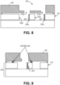
- both uniform and non-uniform step coverage may be achieved using the multi-level shadow mask 200.
- the shadow mask top level and bottom level opening sizes 205 and 210, respectively, along with the process conditions, may be optimized to produce either uniform coating across the height of the optical surface 280, as shown in FIG. 7A , or non-uniform coating, as shown in FIG. 7B .
- the non-uniform coating can lead to, for example, a wedge shape of the coating material 285, as can be seen in FIG. 7B .
- the shadow mask 200 may include a single large top level opening 205 overlapping two or more bottom level openings 210a and 210b.
- the top level opening 205 may provide the same thin film thickness on both optical surfaces 280a and 280b of the micro-optical bench device 270.
- the bottom level openings 210a and 210b may be used to control the spread of the thin film material 285 and to protect other non-coated surfaces 290a and 290b.
- FIG. 9 illustrates an exemplary shadow mask 200 including spacers 900 between the shadow mask 200 and the substrate 230, in accordance with aspects of the present disclosure.
- the spacers 900 may control the thin film thickness across the wafer and prevent stress on the shadow mask 200, thus preventing bending of the shadow mask 200.
- the spacers 900 may be distributed between the shadow mask 200 and the substrate/wafer 230 before singulation. In one example, the spacers 900 may be distributed in the bottom level (i.e., recessed portion) of the shadow mask 200 and may be etched in the shadow mask using a photolithographic mask on the bottom surface of the shadow mask 200.
- the spacers 900 may be positioned in the bottom level so as to not overlap with the moving/fragile micro-fabricated structures 282 in the micro-optical bench device 270.
- the stoppers 900 may maintain a nearly constant gap between the recessed bottom surface of the shadow mask 200 and the top surface of the substrate 230, and thus, may improve uniformity of metallization across the substrate/wafer 230.
- FIG. 10 is a top view of a layout of an exemplary multi-level shadow mask 200, in accordance with aspects of the present disclosure.
- the bottom level opening 210 can be seen through the top level opening 205 in the shadow mask 200.
- the bottom level opening 210 includes several sub-openings 210a-210d aligned in different directions to produce the desired thin film coating on the micro-optical bench device 270 (shown as a dotted line).
- the micro-optical bench device 270 shown in FIG. 10 forms at least a part of an optical interferometer including a micro-mirror to be metallized and an interface (e.g., a beam splitter) to be protected from metallization.
- one sub-opening may be designed to minimize the opening size in the direction connecting the micro-mirror surface 280 to be metallized and the interface surface 290 to be protected.
- Another sub-opening e.g., sub-opening 210b
- the bottom level opening 210 may include a union of at least one rectangular shape and at least one parallelogram shape, where the parallelogram shape forms an opening that is tilted with respect to the rectangular shape.
- FIG. 11 An example of a spectrometer including an interferometer that may be fabricated as a micro-optical bench device is shown in FIG. 11 .
- the spectrometer 1100 includes a Michelson interferometer 1105.
- other types of interferometers such as Fabry-Perot and Mach-Zehnder interferometers, may be utilized.
- collimated light I 0 from a broadband source 1110 is split into two beams I 1 and I 2 by a beam splitter 1120.
- One beam I 1 is reflected off a fixed mirror 1130 and the other beam I 2 is reflected off a moving mirror 1140 coupled to an actuator 1150, such as a MEMS actuator.
- an actuator 1150 such as a MEMS actuator.
- the (light) coupling efficiency of the interferometer 1150 may be maximized by optimizing the step coverage uniformity of the metal layer along the height of the fixed and moveable mirrors 1130 and 1140 using a multi-level shadow mask 200, as discussed above.
- the MEMS actuator 1150 is formed of a comb drive and spring.
- a voltage to the comb drive By applying a voltage to the comb drive, a potential difference results across the actuator 1150, which induces a capacitance therein, causing a driving force to be generated as well as a restoring force from the spring, thereby causing a displacement of moveable mirror 1140 to the desired position for reflection of the beam L 2 .
- An optical path length difference (OPD) is then created between the reflected beams that is substantially equal to twice the mirror 1140 displacement.
- the reflected beams interfere at the beam splitter 1120, allowing the temporal coherence of the light to be measured at each different Optical Path Difference (OPD) offered by the moving mirror.
- OPD Optical Path Difference
- the signal called the interferogram, is measured by a detector 1160 at many discrete positions of the moving mirror.
- the spectrum may then be retrieved, for example, using a Fourier transform carried out by a processor 1170.
- the processor 1170 may be a single processing device or a plurality of processing devices.
- a processing device may be a microprocessor, micro-controller, digital signal processor, microcomputer, central processing unit, field programmable gate array, programmable logic device, logic circuitry, analog circuitry, digital circuitry, and/or any device that manipulates signals (analog and/or digital) based on hard coding of the circuitry and/or operational instructions.
- the processor 1170 may have an associated memory and/or memory element, which may be a single memory device, a plurality of memory devices, and/or embedded circuitry of the processor.
- Such a memory device may be a read-only memory, random access memory, volatile memory, non-volatile memory, static memory, dynamic memory, flash memory, cache memory, and/or any device that stores digital information.
- FIG. 12 is a flowchart illustrating an exemplary method 1200 for selective coating of micro-fabricated structures within a micro-optical bench device using a multi-level shadow mask, in accordance with aspects of the present disclosure.
- the method 1200 begins at block 1210 by providing a substrate including micro-fabricated structures forming a micro-optical bench device.
- a multi-level shadow mask is provided that includes a first opening within a top surface of the shadow mask and a second opening within a bottom surface of the shadow mask.
- the second opening is aligned with the first opening and has a width less than the width of the first opening, such that an overlap between the first opening and the second opening form a hole within the shadow mask.
- the shadow mask is placed on the substrate in a position to enable a surface of a micro-fabricated structure to be coated through the hole.
- the bottom surface of the shadow mask is placed adjacent to a top surface of the substrate and the micro-fabricated structure surface to be coated is aligned with the hole.
- a coating material such as a metal layer, is deposited on the surface of the micro-fabricated structure through the hole.
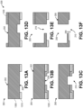
- FIGs. 13A-13F illustrate an exemplary process for fabricating a multi-level shadow mask 200, in accordance with aspects of the present disclosure.
- a substrate 1300 for the shadow mask is provided and a recess pattern 1310 is formed on a bottom surface 204 of the substrate 1300 through a lithography step.
- the recess pattern 1310 may be formed, for example, by depositing a layer of aluminum on the bottom surface 204 of the substrate 1300 and patterning the layer of aluminum to form the recess pattern 1310.
- a layer of photo-resist 1320 is deposited on the bottom surface 204 of the substrate 1300 and patterned to form a bottom opening pattern.
- the bottom opening 210 is etched in the substrate 1300 through the bottom opening pattern for a predefined depth.
- FIG. 13D another layer of photo-resist 1330 is deposited on the top surface 202 of the substrate 1300 and patterned to form a top opening pattern.
- FIG. 13E the top opening 205 is etched in the substrate 1300 through the top opening pattern until the top opening 205 meets the bottom opening 210, and a hole 215 forms in the substrate 1300.
- FIG. 13F the shadow mask recess portion 206 is etched using the recess pattern 1310 to ensure the shadow mask 200 does not come into contact with any movable/fragile micro-fabricated structures while using the shadow mask for step coverage.
Landscapes
- Chemical & Material Sciences (AREA)
- Engineering & Computer Science (AREA)
- Microelectronics & Electronic Packaging (AREA)
- Manufacturing & Machinery (AREA)
- Mechanical Engineering (AREA)
- Organic Chemistry (AREA)
- Materials Engineering (AREA)
- Chemical Kinetics & Catalysis (AREA)
- Metallurgy (AREA)
- General Chemical & Material Sciences (AREA)
- Physics & Mathematics (AREA)
- General Physics & Mathematics (AREA)
- Condensed Matter Physics & Semiconductors (AREA)
- Computer Hardware Design (AREA)
- Power Engineering (AREA)
- Physical Vapour Deposition (AREA)
- Micromachines (AREA)
- Mechanical Light Control Or Optical Switches (AREA)
- Optics & Photonics (AREA)
Claims (14)
- Verfahren zum selektiven Beschichten außerhalb der Ebene liegender Flächen von mikrogefertigten Strukturen innerhalb einer Vorrichtung, umfassend:Bereitstellen eines Substrats (230), das die mikrogefertigten Strukturen beinhaltet;Bereitstellen einer Schattenmaske (200), die eine erste Öffnung (205) in einer obenliegenden Fläche (202) der Schattenmaske (200) und eine zweite Öffnung (210) in einer untenliegenden Fläche (204) der Schattenmaske (200) beinhaltet, wobei die zweite Öffnung (210) auf die erste Öffnung (205) ausgerichtet ist und eine zweite Weite (Lmb) aufweist, welche geringer als eine erste Weite (Lm) der ersten Öffnung (205) ist, wobei eine erste Überlappung zwischen der ersten Öffnung (205) und der zweiten Öffnung (210) ein erstes Loch (215) in der Schattenmaske (200) bildet;Anordnen der Schattenmaske (200) auf dem Substrat (230), derart, dass die untenliegende Fläche (204) der Schattenmaske (200) dem Substrat (230) zugewandt ist; undAbscheiden eines Beschichtungsmaterials (285) auf einer ersten Fläche (280) einer ersten mikrogefertigten Struktur (282) durch das erste Loch (215), wobei die erste Fläche (280) unter Bezugnahme auf das Substrat (230) außerhalb der Ebene liegt;wobei es sich bei der Schattenmaske (200) um eine Schattenmaske mit mehreren Ebenen handelt, die eine erste Dicke (D1), welche einer ersten Tiefe des ersten Lochs (215) entspricht, eine zweite Dicke (D2), welche größer als die erste Dicke (D1) ist und einer Gesamtdicke der Schattenmaske (200) entspricht, und eine dritte Dicke (D3) umfasst, welche geringer als die erste Dicke (D1) ist und einer zweiten Tiefe der zweiten Öffnung (210) entspricht;wobei sich die dritte Dicke (D3) ausgehend von der untenliegenden Fläche (204) der Schattenmaske (200) erstreckt; undwobei die erste Öffnung (205) sich ausgehend von der obenliegenden Fläche (202) durch eine vierte Dicke erstreckt, welche einem Unterschied zwischen der ersten Dicke (D1) und der dritten Dicke (D3) entspricht;dadurch gekennzeichnet, dass der Schritt des Bereitstellens der Schattenmaske weiterhin das Bilden einer Schutzlippe (220) entlang der untenliegenden Fläche (204) der Schattenmaske (200) umfasst, wobei die Schutzlippe (220) eine dritte Weite aufweist, welche einem Unterschied zwischen der ersten Weite (Lm) der ersten Öffnung (205) und der zweiten Weite (Lmb) der zweiten Öffnung (210) entspricht;wobei eine Seitenwand des Lochs sich durch die erste Dicke (D1) erstreckt, indem die erste Öffnung (205) und die zweite Öffnung (210) auf einer Seite des Lochs aufeinander ausgerichtet werden; undwobei die dritte Dicke (D3) ausschließlich auf der anderen Seite des Lochs, welche der Seitenwand entgegengesetzt ist, eine Schutzlippe (220) bildet.
- Verfahren nach Anspruch 1, weiterhin Folgendes umfassend:Schützen einer zweiten Fläche (290) einer zweiten mikrogefertigten Struktur (292) während des Abscheidens des Beschichtungsmaterials unter Verwendung der Schutzlippe (220); undmöglichst geringes Auslegen eines Abstands zwischen der ersten Fläche (280) der ersten mikrogefertigten Struktur (282) und der zweiten Fläche (290) der zweiten mikrogefertigten Struktur (292), auf Grundlage der ersten Weite (Lm) der ersten Öffnung (205), der ersten Dicke (D1) der Schattenmaske (200) und der dritten Dicke (D3) der Schattenmaske (200).
- Verfahren nach Anspruch 2, wobei die Vorrichtung ein Interferometer beinhaltet, die erste mikrogefertigte Struktur (282) einen Mikrospiegel beinhaltet und die zweite mikrogefertigte Struktur (292) einen Strahlteiler beinhaltet; und
wobei das Abscheiden des Beschichtungsmaterials weiterhin ein möglichst großes Auslegen einer Kopplungswirksamkeit des Interferometers umfasst, indem die Gleichmäßigkeit der Stufenbedeckung der Metallschicht entlang einer Höhe des Mikrospiegels optimiert wird. - Verfahren nach Anspruch 1, wobei es sich bei der ersten Öffnung (205) um eine erste oben befindliche Öffnung handelt und es sich bei der zweiten Öffnung (210) und eine erste unten befindliche Öffnung handelt, wobei das Bereitstellen der Schattenmaske weiterhin Folgendes umfasst:Bereitstellen einer zweiten oben befindlichen Öffnung in der obenliegenden Fläche der Schattenmaske, undBereitstellen einer zweiten unten befindlichen Öffnung, die getrennt von der ersten unten befindlichen Öffnung in der untenliegenden Fläche der Schattenmaske ist;wobei die zweite unten befindliche Öffnung auf die zweite oben befindliche Öffnung ausgerichtet ist und eine vierte Weite aufweist, die geringer als eine dritte Weite der zweiten oben befindlichen Öffnung ist, wobei eine zweite Überlappung zwischen der zweiten oben befindlichen Öffnung und der zweiten unten befindlichen Öffnung ein zweites Loch in der Schattenmaske bildet;und wobei das Verfahren weiterhin ein Abscheiden des Beschichtungsmaterials auf einer optischen Fläche einer dritten mikrogefertigten Struktur durch das zweite Loch umfasst.
- Verfahren nach Anspruch 4, wobei die dritte Weite der zweiten oben befindlichen Öffnung sich von der ersten Weite der ersten, sich oben befindlichen Öffnung unterscheidet; und
wobei das Abscheiden des Beschichtungsmaterials weiterhin ein Steuern der jeweiligen Dicke des Beschichtungsmaterials, welches auf der ersten Fläche der ersten mikrogefertigten Struktur und der optischen Fläche der dritten mikrogefertigten Struktur abgeschieden wird, auf Grundlage eines Unterschieds zwischen der ersten Weite der ersten oben befindlichen Öffnung und der dritten Weite der zweiten oben befindlichen Öffnung umfasst. - Verfahren nach Anspruch 1, wobei das Bereitstellen der Schattenmaske weiterhin Folgendes umfasst:Bereitstellen einer ersten mit einem Muster versehenen Maske auf der untenliegenden Fläche der Schattenmaske (200), wobei sich in der ersten mit einem Muster versehenen Maske eine erste Maskenöffnung befindet;Ätzen der untenliegenden Fläche (204) der Schattenmaske durch die erste Maskenöffnung, um die zweite Öffnung (210) auf der untenliegenden Fläche (204) der Schattenmaske zu bilden;Bereitstellen einer zweiten mit einem Muster versehenen Maske auf der obenliegenden Fläche (202) der Schattenmaske, wobei sich in der zweiten mit einem Muster versehenen Maske eine zweite Maskenöffnung befindet; undÄtzen der obenliegenden Fläche der Schattenmaske durch die zweite Maskenöffnung, um die erste Öffnung (205) auf der obenliegenden Fläche der Schattenmaske zu bilden;und wobei sowohl beim Ätzen der obenliegenden Fläche (202), um die erste Öffnung (205) zu bilden, und beim Ätzen der untenliegenden Fläche (204), um die zweite Öffnung zu bilden, reaktives Ionentiefenätzen (DRIE) zur Anwendung gebracht wird.
- Schattenmaske zum selektiven Beschichten außerhalb der Ebene liegender Flächen von mikrogefertigten Strukturen innerhalb einer Vorrichtung, wobei die Schattenmaske Folgendes umfasst:ein Substrat, das eine obenliegende Fläche (202) und eine untenliegende Fläche (204) aufweist;eine erste Öffnung (205) in der obenliegenden Fläche (202) des Substrats; undeine zweite Öffnung (210) in der untenliegenden Fläche (204) des Substrats;wobei die zweite Öffnung (210) auf die erste Öffnung (205) ausgerichtet ist und eine zweite Weite (Lmb) aufweist, welche geringer als die erste Weite (Lm) der ersten Öffnung (205) ist;wobei eine erste Überlappung zwischen der ersten Öffnung (205) und der zweiten Öffnung (210) ein erstes Loch (215) in der Schattenmaske (200) bildet;wobei es sich bei der Schattenmaske (200) um eine Schattenmaske mit mehreren Ebenen handelt, die eine erste Dicke (D1), welche einer ersten Tiefe des ersten Lochs (215) entspricht, eine zweite Dicke (D2), welche größer als die erste Dicke (D1) ist und einer Gesamtdicke des Substrats entspricht, und eine dritte Dicke (D3) umfasst, welche geringer als die erste Dicke (D1) ist und einer zweiten Tiefe der zweiten Öffnung (210) entspricht;wobei sich die dritte Dicke (D3) ausgehend von der untenliegenden Fläche (204) des Substrats erstreckt;wobei die erste Öffnung (205) sich ausgehend von der obenliegenden Fläche (202) durch eine vierte Dicke erstreckt, welche dem Unterschied zwischen der ersten Dicke (D1) und der dritten Dicke (D3) entspricht;dadurch gekennzeichnet, dass die Schattenmaske weiterhin Folgendes umfasst:eine Schutzlippe (220) entlang der untenliegenden Fläche (204), wobei die Schutzlippe (220) eine dritte Weite hat, welche dem Unterschied zwischen der ersten Weite (Lm) der ersten Öffnung (205) und der zweiten Weite (Lmb) der zweiten Öffnung (210) entspricht;wobei die untenliegende Fläche (204) derart ausgestaltet ist, dass sie der Vorrichtung zugewandt ist;wobei eine Seitenwand des Lochs sich durch die erste Dicke (D1) erstreckt, indem die erste Öffnung (205) und die zweite Öffnung (210) auf einer Seite des Lochs aufeinander ausgerichtet werden; undwobei die dritte Dicke (D3) ausschließlich auf der anderen Seite des Lochs, die der Seitenwand entgegengesetzt ist, eine Schutzlippe (220) bildet.
- Schattenmaske nach Anspruch 7, wobei sie weiterhin Folgendes umfasst:
mindestens einen Abstandhalter auf der untenliegenden Seite (204) des Substrats, wobei der mindestens eine Abstandhalter eine fünfte Dicke aufweist, welche dem Unterschied zwischen der ersten Dicke (D1) und der zwischen Dicke (D2) entspricht. - Schattenmaske nach Anspruch 7, wobei es sich bei der ersten Öffnung (205) um eine erste oben befindliche Öffnung handelt und es sich bei der zweiten Öffnung (210) und eine erste unten befindliche Öffnung handelt, und sie weiterhin Folgendes umfasst:eine zweite oben befindliche Öffnung in der obenliegenden Fläche (202) des Substrats;eine zweite unten befindliche Öffnung, die getrennt von der ersten unten befindlichen Öffnung in der untenliegenden Fläche (204) des Substrats ist;wobei die zweite unten befindliche Öffnung auf die zweite oben befindliche Öffnung ausgerichtet ist und eine vierte Weite aufweist, die geringer als eine dritte Weite der dritten Öffnung ist, wobei eine zweite Überlappung zwischen der zweiten oben befindlichen Öffnung und der zweiten unten befindlichen Öffnung ein zweites Loch in dem Substrat bildet.
- Schattenmaske nach Anspruch 9, wobei die dritte Weite der zweiten oben befindlichen Öffnung sich von der ersten Weite der ersten oben befindlichen Öffnung unterscheidet.
- Schattenmaske nach Anspruch 9, wobei die vierte Weite der zweiten unten befindlichen Öffnung sich von der zweiten Weite der ersten unten befindlichen Öffnung unterscheidet.
- Schattenmaske nach Anspruch 9, wobei sie weiterhin Folgendes umfasst:
eine dritte oben befindliche Öffnung in der oben liegenden Fläche des Substrats, wobei die dritte oben befindliche Öffnung die erste oben befindliche Öffnung und die zweite oben befindliche Öffnung beinhaltet. - Schattenmaske nach Anspruch 7, wobei sie weiterhin Folgendes umfasst:eine erste Teilöffnung (210a) in der zweiten Öffnung des Substrats, wobei die erste Teilöffnung eine erste Öffnungsgröße hat; undeine zweite Teilöffnung (210b) in der zweiten Öffnung des Substrats, wobei die zweite Teilöffnung eine zweite Öffnungsgröße hat, welche größer als die erste Öffnungsgröße ist.
- Schattenmaske nach Anspruch 13, wobei die zweite Teilöffnung sich in derselben Ebene wie die erste Teilöffnung befindet und unter Bezugnahme auf die erste Teilöffnung gekippt ist.
Applications Claiming Priority (3)
| Application Number | Priority Date | Filing Date | Title |
|---|---|---|---|
| US201562119065P | 2015-02-20 | 2015-02-20 | |
| US15/047,032 US10562055B2 (en) | 2015-02-20 | 2016-02-18 | Selective step coverage for micro-fabricated structures |
| PCT/US2016/018802 WO2016134329A1 (en) | 2015-02-20 | 2016-02-19 | Selective step coverage for micro-fabricated structures |
Publications (3)
| Publication Number | Publication Date |
|---|---|
| EP3259227A1 EP3259227A1 (de) | 2017-12-27 |
| EP3259227B1 true EP3259227B1 (de) | 2025-01-01 |
| EP3259227C0 EP3259227C0 (de) | 2025-01-01 |
Family
ID=55521817
Family Applications (1)
| Application Number | Title | Priority Date | Filing Date |
|---|---|---|---|
| EP16709197.4A Active EP3259227B1 (de) | 2015-02-20 | 2016-02-19 | Selektive gestufte beschichtung für mikrogefertigte strukturen |
Country Status (5)
| Country | Link |
|---|---|
| US (2) | US10562055B2 (de) |
| EP (1) | EP3259227B1 (de) |
| JP (1) | JP6989382B2 (de) |
| CN (1) | CN107250033B (de) |
| WO (1) | WO2016134329A1 (de) |
Families Citing this family (15)
| Publication number | Priority date | Publication date | Assignee | Title |
|---|---|---|---|---|
| CN106086782B (zh) * | 2016-06-28 | 2018-10-23 | 京东方科技集团股份有限公司 | 一种掩膜版组件及其安装方法、蒸镀装置 |
| KR102671457B1 (ko) * | 2017-11-06 | 2024-05-30 | 매직 립, 인코포레이티드 | 쉐도우 마스크를 사용한 튜닝가능한 구배 패터닝을 위한 방법 |
| US11047039B2 (en) * | 2018-01-08 | 2021-06-29 | Applied Materials, Inc. | Substrate carrier having hard mask |
| CN108726474A (zh) * | 2018-06-05 | 2018-11-02 | 中国电子科技集团公司第二十六研究所 | 一种制作三维电极图形的辅助装置 |
| JP2020122740A (ja) * | 2019-01-31 | 2020-08-13 | セイコーエプソン株式会社 | 構造体形成方法およびデバイス |
| CN110699662B (zh) * | 2019-10-21 | 2022-05-27 | 江苏菲沃泰纳米科技股份有限公司 | 镀膜方法及其膜层 |
| EP4050121A4 (de) | 2019-10-21 | 2024-04-17 | Jiangsu Favored Nanotechnology Co., Ltd. | Verfahren zur beschichtung und filmschicht dafür sowie beschichtungsvorrichtung und verwendung derselben |
| US11335531B2 (en) | 2020-02-13 | 2022-05-17 | Applied Materials, Inc. | Shadow mask apparatus and methods for variable etch depths |
| CN111893432B (zh) * | 2020-08-11 | 2022-11-29 | 京东方科技集团股份有限公司 | 一种掩膜板及其制作方法、显示基板及其制作方法 |
| US20220100078A1 (en) * | 2020-09-25 | 2022-03-31 | Applied Materials, Inc. | Devices and methods for variable etch depths |
| CN218413054U (zh) * | 2021-04-30 | 2023-01-31 | 意法半导体股份有限公司 | 微机电反射镜设备、微投影仪装置和便携式电子装置 |
| IT202100011039A1 (it) | 2021-04-30 | 2022-10-30 | St Microelectronics Srl | Procedimento per la fabbricazione di un dispositivo microelettromeccanico a specchio e dispositivo microelettromeccanico a specchio |
| CN115786844A (zh) * | 2021-09-10 | 2023-03-14 | 北京华卓精科科技股份有限公司 | 改善沉积薄膜厚度均匀性的方法及其掩膜板 |
| US20230333294A1 (en) * | 2022-04-14 | 2023-10-19 | California Institute Of Technology | Non-Uniform-Thickness Layers and Methods for Forming |
| DE102024204674A1 (de) * | 2024-05-21 | 2025-11-27 | Robert Bosch Gesellschaft mit beschränkter Haftung | Verfahren zum Strukturieren und/oder Beschichten bereits vorstrukturierter und/oder vorbeschichteter Substratoberflächen eines Produktwafers |
Citations (3)
| Publication number | Priority date | Publication date | Assignee | Title |
|---|---|---|---|---|
| US20110177637A1 (en) * | 2000-07-12 | 2011-07-21 | 3M Innovative Properties Company | Encapsulated organic electronic devices and method for making same |
| US20130015444A1 (en) * | 2011-07-12 | 2013-01-17 | Sony Corporation | Evaporation mask, method of manufacturing evaporation mask, electronic device, and method of manufacturing electronic device |
| US20130299345A1 (en) * | 2012-05-09 | 2013-11-14 | Iza Corporation | Sputtering apparatus |
Family Cites Families (21)
| Publication number | Priority date | Publication date | Assignee | Title |
|---|---|---|---|---|
| JPS5776842A (en) | 1980-10-31 | 1982-05-14 | Fujitsu Ltd | Pattern forming method |
| JPH06104206A (ja) * | 1992-09-18 | 1994-04-15 | Seiko Instr Inc | 半導体装置の製造方法および製造装置 |
| JPH0987828A (ja) * | 1995-09-28 | 1997-03-31 | Murata Mfg Co Ltd | 電子部品の電極を形成する方法およびそれに用いる装置 |
| TW480572B (en) * | 2001-04-11 | 2002-03-21 | Princo Corp | Vacuum vapor deposition apparatus |
| US6884327B2 (en) * | 2002-03-16 | 2005-04-26 | Tao Pan | Mode size converter for a planar waveguide |
| JP2006002243A (ja) | 2004-06-21 | 2006-01-05 | Seiko Epson Corp | マスク、マスクの製造方法、成膜方法、電子デバイス、及び電子機器 |
| US20060021869A1 (en) * | 2004-07-28 | 2006-02-02 | Advantech Global, Ltd | System for and method of ensuring accurate shadow mask-to-substrate registration in a deposition process |
| JP2006199998A (ja) * | 2005-01-20 | 2006-08-03 | Seiko Epson Corp | 成膜装置、成膜方法 |
| JP4438710B2 (ja) * | 2005-07-20 | 2010-03-24 | セイコーエプソン株式会社 | マスク、マスクチップ、マスクの製造方法及びマスクチップの製造方法 |
| US7485956B2 (en) | 2005-08-16 | 2009-02-03 | Tessera, Inc. | Microelectronic package optionally having differing cover and device thermal expansivities |
| US7796267B2 (en) | 2006-09-28 | 2010-09-14 | Si-Ware Systems | System, method and apparatus for a micromachined interferometer using optical splitting |
| JP2008264137A (ja) * | 2007-04-18 | 2008-11-06 | Topcon Corp | 角膜観察装置 |
| JP2011074404A (ja) * | 2009-09-29 | 2011-04-14 | Nippon Seiki Co Ltd | 蒸着用マスク |
| US9046690B2 (en) | 2011-10-20 | 2015-06-02 | Si-Ware Systems | Integrated monolithic optical bench containing 3-D curved optical elements and methods of its fabrication |
| TWI456080B (zh) * | 2012-07-17 | 2014-10-11 | Wintek Corp | 遮罩組件及使用其之有機氣相沉積裝置與熱蒸鍍裝置 |
| KR102124040B1 (ko) * | 2013-02-01 | 2020-06-29 | 삼성디스플레이 주식회사 | 박막 증착용 마스크, 이의 제조 방법, 및 이를 이용한 유기 발광 표시 장치의 제조 방법 |
| WO2014119548A1 (ja) * | 2013-02-04 | 2014-08-07 | シャープ株式会社 | 蒸着装置および蒸着方法 |
| KR102134363B1 (ko) * | 2013-09-10 | 2020-07-16 | 삼성디스플레이 주식회사 | 메탈 마스크 제작 방법 및 이를 이용한 메탈 마스크 |
| CN103589996A (zh) * | 2013-10-09 | 2014-02-19 | 昆山允升吉光电科技有限公司 | 一种掩模板 |
| CN103882375B (zh) * | 2014-03-12 | 2016-03-09 | 京东方科技集团股份有限公司 | 一种掩膜板及其制作方法 |
| CN203999787U (zh) | 2014-08-12 | 2014-12-10 | 北京维信诺科技有限公司 | 一种蒸镀掩膜版 |
-
2016
- 2016-02-18 US US15/047,032 patent/US10562055B2/en active Active
- 2016-02-19 WO PCT/US2016/018802 patent/WO2016134329A1/en not_active Ceased
- 2016-02-19 CN CN201680011162.2A patent/CN107250033B/zh active Active
- 2016-02-19 JP JP2017542406A patent/JP6989382B2/ja active Active
- 2016-02-19 EP EP16709197.4A patent/EP3259227B1/de active Active
-
2019
- 2019-12-30 US US16/730,947 patent/US11499218B2/en active Active
Patent Citations (3)
| Publication number | Priority date | Publication date | Assignee | Title |
|---|---|---|---|---|
| US20110177637A1 (en) * | 2000-07-12 | 2011-07-21 | 3M Innovative Properties Company | Encapsulated organic electronic devices and method for making same |
| US20130015444A1 (en) * | 2011-07-12 | 2013-01-17 | Sony Corporation | Evaporation mask, method of manufacturing evaporation mask, electronic device, and method of manufacturing electronic device |
| US20130299345A1 (en) * | 2012-05-09 | 2013-11-14 | Iza Corporation | Sputtering apparatus |
Also Published As
| Publication number | Publication date |
|---|---|
| US11499218B2 (en) | 2022-11-15 |
| EP3259227A1 (de) | 2017-12-27 |
| EP3259227C0 (de) | 2025-01-01 |
| JP6989382B2 (ja) | 2022-01-05 |
| US20160246010A1 (en) | 2016-08-25 |
| US20200130006A1 (en) | 2020-04-30 |
| US10562055B2 (en) | 2020-02-18 |
| CN107250033B (zh) | 2020-10-09 |
| CN107250033A (zh) | 2017-10-13 |
| WO2016134329A1 (en) | 2016-08-25 |
| JP2018508375A (ja) | 2018-03-29 |
Similar Documents
| Publication | Publication Date | Title |
|---|---|---|
| US11499218B2 (en) | Selective step coverage for micro-fabricated structures | |
| EP3803957B1 (de) | Steuerung von ätzwinkeln durch substratdrehung bei winkelätzwerkzeugen | |
| US9618323B2 (en) | Method for manufacturing optical interferometer | |
| JP5860809B2 (ja) | マイクロ電子機械的システム(mems)干渉計 | |
| US7796267B2 (en) | System, method and apparatus for a micromachined interferometer using optical splitting | |
| JP4713464B2 (ja) | 中空コアの導波路を含む可変光減衰器 | |
| US20010008457A1 (en) | Microelectromechanical optical switch and method of manufacture thereof | |
| US7903318B2 (en) | MEMS micromirror devices with anti-reflective structures | |
| JP2014522510A (ja) | 調整可能なマイクロメカニカルファブリー・ペローの干渉計およびその製造方法 | |
| CN103582830A (zh) | 光学部件的制造方法以及光学部件 | |
| US10120134B2 (en) | Micro-optical bench device with highly/selectively-controlled optical surfaces | |
| US8508745B2 (en) | System, method and apparatus for a micromachined interferometer using optical splitting | |
| US20210033847A1 (en) | Micromechanical Mirror Device, Mirror System, and Method for Producing a Micromechanical Mirror Device | |
| US8885245B2 (en) | Biaxial MEMS mirror with hidden hinge and staggered electrodes | |
| JP4069041B2 (ja) | エッチング用マスク及びその形成方法 | |
| WO2006096724A2 (en) | Mechanically-active anti-reflection switch (mars) modulator with wide angle tolerance |
Legal Events
| Date | Code | Title | Description |
|---|---|---|---|
| STAA | Information on the status of an ep patent application or granted ep patent |
Free format text: STATUS: THE INTERNATIONAL PUBLICATION HAS BEEN MADE |
|
| PUAI | Public reference made under article 153(3) epc to a published international application that has entered the european phase |
Free format text: ORIGINAL CODE: 0009012 |
|
| STAA | Information on the status of an ep patent application or granted ep patent |
Free format text: STATUS: REQUEST FOR EXAMINATION WAS MADE |
|
| 17P | Request for examination filed |
Effective date: 20170919 |
|
| AK | Designated contracting states |
Kind code of ref document: A1 Designated state(s): AL AT BE BG CH CY CZ DE DK EE ES FI FR GB GR HR HU IE IS IT LI LT LU LV MC MK MT NL NO PL PT RO RS SE SI SK SM TR |
|
| AX | Request for extension of the european patent |
Extension state: BA ME |
|
| DAV | Request for validation of the european patent (deleted) | ||
| DAX | Request for extension of the european patent (deleted) | ||
| STAA | Information on the status of an ep patent application or granted ep patent |
Free format text: STATUS: EXAMINATION IS IN PROGRESS |
|
| 17Q | First examination report despatched |
Effective date: 20190219 |
|
| GRAP | Despatch of communication of intention to grant a patent |
Free format text: ORIGINAL CODE: EPIDOSNIGR1 |
|
| STAA | Information on the status of an ep patent application or granted ep patent |
Free format text: STATUS: GRANT OF PATENT IS INTENDED |
|
| RIC1 | Information provided on ipc code assigned before grant |
Ipc: B81C 1/00 20060101AFI20240916BHEP |
|
| INTG | Intention to grant announced |
Effective date: 20241014 |
|
| GRAS | Grant fee paid |
Free format text: ORIGINAL CODE: EPIDOSNIGR3 |
|
| GRAA | (expected) grant |
Free format text: ORIGINAL CODE: 0009210 |
|
| STAA | Information on the status of an ep patent application or granted ep patent |
Free format text: STATUS: THE PATENT HAS BEEN GRANTED |
|
| AK | Designated contracting states |
Kind code of ref document: B1 Designated state(s): AL AT BE BG CH CY CZ DE DK EE ES FI FR GB GR HR HU IE IS IT LI LT LU LV MC MK MT NL NO PL PT RO RS SE SI SK SM TR |
|
| REG | Reference to a national code |
Ref country code: GB Ref legal event code: FG4D |
|
| REG | Reference to a national code |
Ref country code: CH Ref legal event code: EP |
|
| REG | Reference to a national code |
Ref country code: DE Ref legal event code: R096 Ref document number: 602016090793 Country of ref document: DE |
|
| REG | Reference to a national code |
Ref country code: IE Ref legal event code: FG4D |
|
| U01 | Request for unitary effect filed |
Effective date: 20250101 |
|
| U07 | Unitary effect registered |
Designated state(s): AT BE BG DE DK EE FI FR IT LT LU LV MT NL PT RO SE SI Effective date: 20250110 |
|
| U20 | Renewal fee for the european patent with unitary effect paid |
Year of fee payment: 10 Effective date: 20250225 |
|
| PG25 | Lapsed in a contracting state [announced via postgrant information from national office to epo] |
Ref country code: PL Free format text: LAPSE BECAUSE OF FAILURE TO SUBMIT A TRANSLATION OF THE DESCRIPTION OR TO PAY THE FEE WITHIN THE PRESCRIBED TIME-LIMIT Effective date: 20250101 |
|
| PG25 | Lapsed in a contracting state [announced via postgrant information from national office to epo] |
Ref country code: ES Free format text: LAPSE BECAUSE OF FAILURE TO SUBMIT A TRANSLATION OF THE DESCRIPTION OR TO PAY THE FEE WITHIN THE PRESCRIBED TIME-LIMIT Effective date: 20250101 |
|
| PG25 | Lapsed in a contracting state [announced via postgrant information from national office to epo] |
Ref country code: IS Free format text: LAPSE BECAUSE OF FAILURE TO SUBMIT A TRANSLATION OF THE DESCRIPTION OR TO PAY THE FEE WITHIN THE PRESCRIBED TIME-LIMIT Effective date: 20250501 Ref country code: NO Free format text: LAPSE BECAUSE OF FAILURE TO SUBMIT A TRANSLATION OF THE DESCRIPTION OR TO PAY THE FEE WITHIN THE PRESCRIBED TIME-LIMIT Effective date: 20250401 |
|
| PG25 | Lapsed in a contracting state [announced via postgrant information from national office to epo] |
Ref country code: HR Free format text: LAPSE BECAUSE OF FAILURE TO SUBMIT A TRANSLATION OF THE DESCRIPTION OR TO PAY THE FEE WITHIN THE PRESCRIBED TIME-LIMIT Effective date: 20250101 |
|
| PG25 | Lapsed in a contracting state [announced via postgrant information from national office to epo] |
Ref country code: GR Free format text: LAPSE BECAUSE OF FAILURE TO SUBMIT A TRANSLATION OF THE DESCRIPTION OR TO PAY THE FEE WITHIN THE PRESCRIBED TIME-LIMIT Effective date: 20250402 |
|
| PG25 | Lapsed in a contracting state [announced via postgrant information from national office to epo] |
Ref country code: CZ Free format text: LAPSE BECAUSE OF FAILURE TO SUBMIT A TRANSLATION OF THE DESCRIPTION OR TO PAY THE FEE WITHIN THE PRESCRIBED TIME-LIMIT Effective date: 20250101 |
|
| REG | Reference to a national code |
Ref country code: CH Ref legal event code: PL |
|
| PG25 | Lapsed in a contracting state [announced via postgrant information from national office to epo] |
Ref country code: SM Free format text: LAPSE BECAUSE OF FAILURE TO SUBMIT A TRANSLATION OF THE DESCRIPTION OR TO PAY THE FEE WITHIN THE PRESCRIBED TIME-LIMIT Effective date: 20250101 |
|
| PG25 | Lapsed in a contracting state [announced via postgrant information from national office to epo] |
Ref country code: MC Free format text: LAPSE BECAUSE OF FAILURE TO SUBMIT A TRANSLATION OF THE DESCRIPTION OR TO PAY THE FEE WITHIN THE PRESCRIBED TIME-LIMIT Effective date: 20250101 |
|
| PG25 | Lapsed in a contracting state [announced via postgrant information from national office to epo] |
Ref country code: CH Free format text: LAPSE BECAUSE OF NON-PAYMENT OF DUE FEES Effective date: 20250228 |
|
| PG25 | Lapsed in a contracting state [announced via postgrant information from national office to epo] |
Ref country code: SK Free format text: LAPSE BECAUSE OF FAILURE TO SUBMIT A TRANSLATION OF THE DESCRIPTION OR TO PAY THE FEE WITHIN THE PRESCRIBED TIME-LIMIT Effective date: 20250101 |
|
| PLBE | No opposition filed within time limit |
Free format text: ORIGINAL CODE: 0009261 |
|
| STAA | Information on the status of an ep patent application or granted ep patent |
Free format text: STATUS: NO OPPOSITION FILED WITHIN TIME LIMIT |