EP3255487B1 - Anzeigevorrichtung und herstellungsverfahren dafür - Google Patents
Anzeigevorrichtung und herstellungsverfahren dafür Download PDFInfo
- Publication number
- EP3255487B1 EP3255487B1 EP15880864.2A EP15880864A EP3255487B1 EP 3255487 B1 EP3255487 B1 EP 3255487B1 EP 15880864 A EP15880864 A EP 15880864A EP 3255487 B1 EP3255487 B1 EP 3255487B1
- Authority
- EP
- European Patent Office
- Prior art keywords
- leads
- display
- cell device
- display apparatus
- pins
- Prior art date
- Legal status (The legal status is an assumption and is not a legal conclusion. Google has not performed a legal analysis and makes no representation as to the accuracy of the status listed.)
- Active
Links
Images


Classifications
-
- G—PHYSICS
- G06—COMPUTING OR CALCULATING; COUNTING
- G06F—ELECTRIC DIGITAL DATA PROCESSING
- G06F3/00—Input arrangements for transferring data to be processed into a form capable of being handled by the computer; Output arrangements for transferring data from processing unit to output unit, e.g. interface arrangements
- G06F3/01—Input arrangements or combined input and output arrangements for interaction between user and computer
- G06F3/03—Arrangements for converting the position or the displacement of a member into a coded form
- G06F3/041—Digitisers, e.g. for touch screens or touch pads, characterised by the transducing means
- G06F3/0416—Control or interface arrangements specially adapted for digitisers
- G06F3/04164—Connections between sensors and controllers, e.g. routing lines between electrodes and connection pads
-
- G—PHYSICS
- G02—OPTICS
- G02F—OPTICAL DEVICES OR ARRANGEMENTS FOR THE CONTROL OF LIGHT BY MODIFICATION OF THE OPTICAL PROPERTIES OF THE MEDIA OF THE ELEMENTS INVOLVED THEREIN; NON-LINEAR OPTICS; FREQUENCY-CHANGING OF LIGHT; OPTICAL LOGIC ELEMENTS; OPTICAL ANALOGUE/DIGITAL CONVERTERS
- G02F1/00—Devices or arrangements for the control of the intensity, colour, phase, polarisation or direction of light arriving from an independent light source, e.g. switching, gating or modulating; Non-linear optics
- G02F1/01—Devices or arrangements for the control of the intensity, colour, phase, polarisation or direction of light arriving from an independent light source, e.g. switching, gating or modulating; Non-linear optics for the control of the intensity, phase, polarisation or colour
- G02F1/15—Devices or arrangements for the control of the intensity, colour, phase, polarisation or direction of light arriving from an independent light source, e.g. switching, gating or modulating; Non-linear optics for the control of the intensity, phase, polarisation or colour based on an electrochromic effect
- G02F1/153—Constructional details
- G02F1/1533—Constructional details structural features not otherwise provided for
-
- G—PHYSICS
- G02—OPTICS
- G02B—OPTICAL ELEMENTS, SYSTEMS OR APPARATUS
- G02B30/00—Optical systems or apparatus for producing three-dimensional [3D] effects, e.g. stereoscopic images
- G02B30/20—Optical systems or apparatus for producing three-dimensional [3D] effects, e.g. stereoscopic images by providing first and second parallax images to an observer's left and right eyes
- G02B30/26—Optical systems or apparatus for producing three-dimensional [3D] effects, e.g. stereoscopic images by providing first and second parallax images to an observer's left and right eyes of the autostereoscopic type
- G02B30/27—Optical systems or apparatus for producing three-dimensional [3D] effects, e.g. stereoscopic images by providing first and second parallax images to an observer's left and right eyes of the autostereoscopic type involving lenticular arrays
- G02B30/28—Optical systems or apparatus for producing three-dimensional [3D] effects, e.g. stereoscopic images by providing first and second parallax images to an observer's left and right eyes of the autostereoscopic type involving lenticular arrays involving active lenticular arrays
-
- G—PHYSICS
- G02—OPTICS
- G02B—OPTICAL ELEMENTS, SYSTEMS OR APPARATUS
- G02B30/00—Optical systems or apparatus for producing three-dimensional [3D] effects, e.g. stereoscopic images
- G02B30/20—Optical systems or apparatus for producing three-dimensional [3D] effects, e.g. stereoscopic images by providing first and second parallax images to an observer's left and right eyes
- G02B30/26—Optical systems or apparatus for producing three-dimensional [3D] effects, e.g. stereoscopic images by providing first and second parallax images to an observer's left and right eyes of the autostereoscopic type
- G02B30/30—Optical systems or apparatus for producing three-dimensional [3D] effects, e.g. stereoscopic images by providing first and second parallax images to an observer's left and right eyes of the autostereoscopic type involving parallax barriers
- G02B30/31—Optical systems or apparatus for producing three-dimensional [3D] effects, e.g. stereoscopic images by providing first and second parallax images to an observer's left and right eyes of the autostereoscopic type involving parallax barriers involving active parallax barriers
-
- G—PHYSICS
- G02—OPTICS
- G02F—OPTICAL DEVICES OR ARRANGEMENTS FOR THE CONTROL OF LIGHT BY MODIFICATION OF THE OPTICAL PROPERTIES OF THE MEDIA OF THE ELEMENTS INVOLVED THEREIN; NON-LINEAR OPTICS; FREQUENCY-CHANGING OF LIGHT; OPTICAL LOGIC ELEMENTS; OPTICAL ANALOGUE/DIGITAL CONVERTERS
- G02F1/00—Devices or arrangements for the control of the intensity, colour, phase, polarisation or direction of light arriving from an independent light source, e.g. switching, gating or modulating; Non-linear optics
- G02F1/01—Devices or arrangements for the control of the intensity, colour, phase, polarisation or direction of light arriving from an independent light source, e.g. switching, gating or modulating; Non-linear optics for the control of the intensity, phase, polarisation or colour
- G02F1/13—Devices or arrangements for the control of the intensity, colour, phase, polarisation or direction of light arriving from an independent light source, e.g. switching, gating or modulating; Non-linear optics for the control of the intensity, phase, polarisation or colour based on liquid crystals, e.g. single liquid crystal display cells
- G02F1/133—Constructional arrangements; Operation of liquid crystal cells; Circuit arrangements
- G02F1/1333—Constructional arrangements; Manufacturing methods
- G02F1/1343—Electrodes
-
- G—PHYSICS
- G02—OPTICS
- G02F—OPTICAL DEVICES OR ARRANGEMENTS FOR THE CONTROL OF LIGHT BY MODIFICATION OF THE OPTICAL PROPERTIES OF THE MEDIA OF THE ELEMENTS INVOLVED THEREIN; NON-LINEAR OPTICS; FREQUENCY-CHANGING OF LIGHT; OPTICAL LOGIC ELEMENTS; OPTICAL ANALOGUE/DIGITAL CONVERTERS
- G02F1/00—Devices or arrangements for the control of the intensity, colour, phase, polarisation or direction of light arriving from an independent light source, e.g. switching, gating or modulating; Non-linear optics
- G02F1/01—Devices or arrangements for the control of the intensity, colour, phase, polarisation or direction of light arriving from an independent light source, e.g. switching, gating or modulating; Non-linear optics for the control of the intensity, phase, polarisation or colour
- G02F1/13—Devices or arrangements for the control of the intensity, colour, phase, polarisation or direction of light arriving from an independent light source, e.g. switching, gating or modulating; Non-linear optics for the control of the intensity, phase, polarisation or colour based on liquid crystals, e.g. single liquid crystal display cells
- G02F1/133—Constructional arrangements; Operation of liquid crystal cells; Circuit arrangements
- G02F1/1333—Constructional arrangements; Manufacturing methods
- G02F1/1345—Conductors connecting electrodes to cell terminals
- G02F1/13452—Conductors connecting driver circuitry and terminals of panels
-
- G—PHYSICS
- G06—COMPUTING OR CALCULATING; COUNTING
- G06F—ELECTRIC DIGITAL DATA PROCESSING
- G06F3/00—Input arrangements for transferring data to be processed into a form capable of being handled by the computer; Output arrangements for transferring data from processing unit to output unit, e.g. interface arrangements
- G06F3/01—Input arrangements or combined input and output arrangements for interaction between user and computer
- G06F3/03—Arrangements for converting the position or the displacement of a member into a coded form
- G06F3/041—Digitisers, e.g. for touch screens or touch pads, characterised by the transducing means
-
- H—ELECTRICITY
- H04—ELECTRIC COMMUNICATION TECHNIQUE
- H04N—PICTORIAL COMMUNICATION, e.g. TELEVISION
- H04N13/00—Stereoscopic video systems; Multi-view video systems; Details thereof
- H04N13/30—Image reproducers
- H04N13/302—Image reproducers for viewing without the aid of special glasses, i.e. using autostereoscopic displays
- H04N13/305—Image reproducers for viewing without the aid of special glasses, i.e. using autostereoscopic displays using lenticular lenses, e.g. arrangements of cylindrical lenses
-
- H—ELECTRICITY
- H04—ELECTRIC COMMUNICATION TECHNIQUE
- H04N—PICTORIAL COMMUNICATION, e.g. TELEVISION
- H04N13/00—Stereoscopic video systems; Multi-view video systems; Details thereof
- H04N13/30—Image reproducers
- H04N13/302—Image reproducers for viewing without the aid of special glasses, i.e. using autostereoscopic displays
- H04N13/31—Image reproducers for viewing without the aid of special glasses, i.e. using autostereoscopic displays using parallax barriers
-
- G—PHYSICS
- G02—OPTICS
- G02B—OPTICAL ELEMENTS, SYSTEMS OR APPARATUS
- G02B30/00—Optical systems or apparatus for producing three-dimensional [3D] effects, e.g. stereoscopic images
- G02B30/20—Optical systems or apparatus for producing three-dimensional [3D] effects, e.g. stereoscopic images by providing first and second parallax images to an observer's left and right eyes
- G02B30/26—Optical systems or apparatus for producing three-dimensional [3D] effects, e.g. stereoscopic images by providing first and second parallax images to an observer's left and right eyes of the autostereoscopic type
- G02B30/27—Optical systems or apparatus for producing three-dimensional [3D] effects, e.g. stereoscopic images by providing first and second parallax images to an observer's left and right eyes of the autostereoscopic type involving lenticular arrays
-
- G—PHYSICS
- G02—OPTICS
- G02F—OPTICAL DEVICES OR ARRANGEMENTS FOR THE CONTROL OF LIGHT BY MODIFICATION OF THE OPTICAL PROPERTIES OF THE MEDIA OF THE ELEMENTS INVOLVED THEREIN; NON-LINEAR OPTICS; FREQUENCY-CHANGING OF LIGHT; OPTICAL LOGIC ELEMENTS; OPTICAL ANALOGUE/DIGITAL CONVERTERS
- G02F1/00—Devices or arrangements for the control of the intensity, colour, phase, polarisation or direction of light arriving from an independent light source, e.g. switching, gating or modulating; Non-linear optics
- G02F1/01—Devices or arrangements for the control of the intensity, colour, phase, polarisation or direction of light arriving from an independent light source, e.g. switching, gating or modulating; Non-linear optics for the control of the intensity, phase, polarisation or colour
- G02F1/13—Devices or arrangements for the control of the intensity, colour, phase, polarisation or direction of light arriving from an independent light source, e.g. switching, gating or modulating; Non-linear optics for the control of the intensity, phase, polarisation or colour based on liquid crystals, e.g. single liquid crystal display cells
- G02F1/133—Constructional arrangements; Operation of liquid crystal cells; Circuit arrangements
- G02F1/1333—Constructional arrangements; Manufacturing methods
- G02F1/13338—Input devices, e.g. touch panels
-
- G—PHYSICS
- G02—OPTICS
- G02F—OPTICAL DEVICES OR ARRANGEMENTS FOR THE CONTROL OF LIGHT BY MODIFICATION OF THE OPTICAL PROPERTIES OF THE MEDIA OF THE ELEMENTS INVOLVED THEREIN; NON-LINEAR OPTICS; FREQUENCY-CHANGING OF LIGHT; OPTICAL LOGIC ELEMENTS; OPTICAL ANALOGUE/DIGITAL CONVERTERS
- G02F1/00—Devices or arrangements for the control of the intensity, colour, phase, polarisation or direction of light arriving from an independent light source, e.g. switching, gating or modulating; Non-linear optics
- G02F1/01—Devices or arrangements for the control of the intensity, colour, phase, polarisation or direction of light arriving from an independent light source, e.g. switching, gating or modulating; Non-linear optics for the control of the intensity, phase, polarisation or colour
- G02F1/13—Devices or arrangements for the control of the intensity, colour, phase, polarisation or direction of light arriving from an independent light source, e.g. switching, gating or modulating; Non-linear optics for the control of the intensity, phase, polarisation or colour based on liquid crystals, e.g. single liquid crystal display cells
- G02F1/133—Constructional arrangements; Operation of liquid crystal cells; Circuit arrangements
- G02F1/1333—Constructional arrangements; Manufacturing methods
- G02F1/1345—Conductors connecting electrodes to cell terminals
-
- G—PHYSICS
- G02—OPTICS
- G02F—OPTICAL DEVICES OR ARRANGEMENTS FOR THE CONTROL OF LIGHT BY MODIFICATION OF THE OPTICAL PROPERTIES OF THE MEDIA OF THE ELEMENTS INVOLVED THEREIN; NON-LINEAR OPTICS; FREQUENCY-CHANGING OF LIGHT; OPTICAL LOGIC ELEMENTS; OPTICAL ANALOGUE/DIGITAL CONVERTERS
- G02F1/00—Devices or arrangements for the control of the intensity, colour, phase, polarisation or direction of light arriving from an independent light source, e.g. switching, gating or modulating; Non-linear optics
- G02F1/01—Devices or arrangements for the control of the intensity, colour, phase, polarisation or direction of light arriving from an independent light source, e.g. switching, gating or modulating; Non-linear optics for the control of the intensity, phase, polarisation or colour
- G02F1/15—Devices or arrangements for the control of the intensity, colour, phase, polarisation or direction of light arriving from an independent light source, e.g. switching, gating or modulating; Non-linear optics for the control of the intensity, phase, polarisation or colour based on an electrochromic effect
- G02F1/153—Constructional details
- G02F1/155—Electrodes
-
- G—PHYSICS
- G02—OPTICS
- G02F—OPTICAL DEVICES OR ARRANGEMENTS FOR THE CONTROL OF LIGHT BY MODIFICATION OF THE OPTICAL PROPERTIES OF THE MEDIA OF THE ELEMENTS INVOLVED THEREIN; NON-LINEAR OPTICS; FREQUENCY-CHANGING OF LIGHT; OPTICAL LOGIC ELEMENTS; OPTICAL ANALOGUE/DIGITAL CONVERTERS
- G02F1/00—Devices or arrangements for the control of the intensity, colour, phase, polarisation or direction of light arriving from an independent light source, e.g. switching, gating or modulating; Non-linear optics
- G02F1/01—Devices or arrangements for the control of the intensity, colour, phase, polarisation or direction of light arriving from an independent light source, e.g. switching, gating or modulating; Non-linear optics for the control of the intensity, phase, polarisation or colour
- G02F1/15—Devices or arrangements for the control of the intensity, colour, phase, polarisation or direction of light arriving from an independent light source, e.g. switching, gating or modulating; Non-linear optics for the control of the intensity, phase, polarisation or colour based on an electrochromic effect
- G02F1/163—Operation of electrochromic cells, e.g. electrodeposition cells; Circuit arrangements therefor
-
- G—PHYSICS
- G02—OPTICS
- G02F—OPTICAL DEVICES OR ARRANGEMENTS FOR THE CONTROL OF LIGHT BY MODIFICATION OF THE OPTICAL PROPERTIES OF THE MEDIA OF THE ELEMENTS INVOLVED THEREIN; NON-LINEAR OPTICS; FREQUENCY-CHANGING OF LIGHT; OPTICAL LOGIC ELEMENTS; OPTICAL ANALOGUE/DIGITAL CONVERTERS
- G02F1/00—Devices or arrangements for the control of the intensity, colour, phase, polarisation or direction of light arriving from an independent light source, e.g. switching, gating or modulating; Non-linear optics
- G02F1/29—Devices or arrangements for the control of the intensity, colour, phase, polarisation or direction of light arriving from an independent light source, e.g. switching, gating or modulating; Non-linear optics for the control of the position or the direction of light beams, i.e. deflection
-
- G—PHYSICS
- G02—OPTICS
- G02F—OPTICAL DEVICES OR ARRANGEMENTS FOR THE CONTROL OF LIGHT BY MODIFICATION OF THE OPTICAL PROPERTIES OF THE MEDIA OF THE ELEMENTS INVOLVED THEREIN; NON-LINEAR OPTICS; FREQUENCY-CHANGING OF LIGHT; OPTICAL LOGIC ELEMENTS; OPTICAL ANALOGUE/DIGITAL CONVERTERS
- G02F2201/00—Constructional arrangements not provided for in groups G02F1/00 - G02F7/00
- G02F2201/44—Arrangements combining different electro-active layers, e.g. electrochromic, liquid crystal or electroluminescent layers
-
- H—ELECTRICITY
- H04—ELECTRIC COMMUNICATION TECHNIQUE
- H04N—PICTORIAL COMMUNICATION, e.g. TELEVISION
- H04N2213/00—Details of stereoscopic systems
- H04N2213/001—Constructional or mechanical details
-
- H—ELECTRICITY
- H05—ELECTRIC TECHNIQUES NOT OTHERWISE PROVIDED FOR
- H05K—PRINTED CIRCUITS; CASINGS OR CONSTRUCTIONAL DETAILS OF ELECTRIC APPARATUS; MANUFACTURE OF ASSEMBLAGES OF ELECTRICAL COMPONENTS
- H05K2201/00—Indexing scheme relating to printed circuits covered by H05K1/00
- H05K2201/10—Details of components or other objects attached to or integrated in a printed circuit board
- H05K2201/10007—Types of components
- H05K2201/10128—Display
-
- H—ELECTRICITY
- H05—ELECTRIC TECHNIQUES NOT OTHERWISE PROVIDED FOR
- H05K—PRINTED CIRCUITS; CASINGS OR CONSTRUCTIONAL DETAILS OF ELECTRIC APPARATUS; MANUFACTURE OF ASSEMBLAGES OF ELECTRICAL COMPONENTS
- H05K3/00—Apparatus or processes for manufacturing printed circuits
- H05K3/36—Assembling printed circuits with other printed circuits
- H05K3/361—Assembling flexible printed circuits with other printed circuits
Definitions
- the present invention relates to the display technical field, particularly to a display apparatus and a manufacturing method thereof.
- a naked-eye three-dimensional liquid crystal display is taken as an example.
- the display panel of the display mainly comprises a first substrate 01, a second substrate 02 and a liquid crystal layer (not shown) sandwiched between the first substrate 01 and the second substrate 02.
- a liquid crystal barrier as the out-cell device of the display mainly comprises a third substrate 03, a fourth substrate 04 and a liquid crystal layer (not shown) sandwiched between the third substrate 03 and the fourth substrate 04.
- the display panel and the out-cell device are both provided with their respective FPCs, i.e., an FPC1 electrically connected to the first substrate 01 and an FPC2 electrically connected to the third substrate 03, as shown in Fig. 1 .
- FPC1 electrically connected to the first substrate 01
- FPC2 electrically connected to the third substrate 03
- the display structure as shown in Fig. 1 needs to additionally make an FPC2 connected to the liquid crystal barrier for three-dimensional display. This would cause an increase in the cost of manufacturing the display and does not facilitate simplification of the structure of the out-cell device.
- CN104049802A discloses such as in Figures 2-3 thereof a touch display apparatus 200, comprising a first substrate 201, a second substrate 202, a display medium layer 203, a flexible circuit board 207, a bonding layer 209, a conductive structure 210 and a driving IC 205, wherein the touch display apparatus 200 further comprises a first electrode lead 206 and a second electrode lead 202a connected to the first electrode lead 206, and the first electrode lead 206 comprises a first sub-pin part 206a electrically connected with the second electrode lead 202a and a second sub-pin part 206b.
- the flexible circuit board 207 comprises a first flexible circuit board electrically connected with the first sub-pin part 206a of the first electrode lead 206 and a second flexible circuit board electrically connected with the second sub-pin part 206b of the second electrode lead 206.
- US 2012/0235948A1 discloses such as in Figure 15 thereof a liquid crystal device, comprising a liquid crystal panel 331, a touch panel 350 and a flexible substrate 640, wherein the flexible substrate 640 comprises two folded sections 645, 646, where a rear surface of the end 642A is connected to the touch panel terminal section 50A of the touch panel 350 through ACF 43B, a front surface of the middle portion 647 is connected to the connecting terminal section 332A through ACF 42B, and the touch panel driver 22 is connected to the front surface of the flexible substrate 640 through ACF 22B.
- US2014/375907A1 discloses such as in Figures 3E-3F thereof a first substrate, a second substrate, a touch electrode unit 33 and at least one conducting unit 34.
- the touch display panel 3d has the conducting units 34 disposed on two neighboring sides of the first substrate 31 to electrically connect the electrodes of the touch electrode unit 33 with different directions to the conductive pattern layer 321. Furthermore, the conducting units 34 on two sides of the first substrate 31 are electrically connected to the touch control IC 38 through the patterned electrodes 3211 and the electrical connection members 39, respectively.
- JP 2009199107A discloses such as in [0014] thereof that the touch-panel lateral electrode 2 and the TFT board substrate lateral electrode 6 are electrically connected by the electrically conductive paste 7.
- One may use a conductive ink, a conductive resin, and a conductive adhesive as the electrically conductive paste 7 here.
- the embodiments of the present invention provide a display apparatus and a manufacturing method thereof, for solving the problems existing in the prior art that the out-cell device of the display apparatus is complex in structure and high in the cost of production.
- the embodiments of the present invention provide a display apparatus, comprising a display device, an out-cell device, and a flexible printed circuit board for being connected to an external signal; wherein,
- the conductive glue is a silver adhesive.
- the first leads and the second leads are arranged in parallel, and the second leads are located at two sides or one side of the first leads.
- the auxiliary device for three-dimensional display is a liquid crystal barrier, an electrochromic grating or a liquid crystal lens.
- the out-cell device comprises a transparent electrode, and the transparent electrode is an interdigitated structure or a laminated structure.
- the embodiments of the present invention further provide a method for manufacturing the aforesaid display apparatus, wherein the out-cell device is an auxiliary device for three-dimensional display, a touch control device or an electrochromic device, the method comprising:
- the embodiments of the present invention provide a display apparatus and a manufacturing method thereof.
- the display apparatus comprises a display device, an out-cell device and a flexible printed circuit board for being connected to an external signal; wherein a binding area of the display device has first leads and second leads; a binding area of the out-cell device has third leads, and the third leads are electrically connected to the second leads; and the flexible printed circuit board has first pins and second pins, the first leads are electrically connected to the first pins, and the second leads are electrically connected to the second pins.
- the third leads are electrically connected to the second leads via a conductive glue, and the conductive glue is further covered with a layer of protective glue.
- the third leads of the out-cell device are electrically connected to the second leads of the display device, while the second leads are electrically connected to the second pins of the flexible printed circuit board, thereby enabling conduction between the out-cell device and the external signal.
- the display apparatus as provided in the embodiments of the present invention omits the step of separately making a flexible printed circuit board of the out-cell device, thereby reducing the cost of production of the display apparatus and at the same time further simplifying the structure of the out-cell device of the display apparatus.
- Covering a layer of protective glue on the conductive glue can prevent the conductive glue from falling off by accident due to direct contact during the processes of manufacturing the display apparatus, thereby ensuring the electrical connection between the third leads of the out-cell device and the second leads of the display device and thus ensuring conduction between the out-cell device and the external signal.
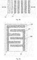
- the embodiments of the present invention provide a display apparatus, which may specifically comprise, as shown in Figure 2 , a display device 1, an out-cell device 2 and a flexible printed circuit board 3 for being connected to an external signal; wherein,
- the aforesaid display apparatus as provided in the embodiments of the present invention comprises a display device 1, an out-cell device 2 and a flexible printed circuit board 3 for being connected to an external signal; wherein a binding area (an area marked with the dashed frame A) of the display device 1 has first leads and second leads (not shown); a binding area (an area marked with the dashed frame B) of the out-cell device 2 has third leads (not shown), and the third leads are electrically connected to the second leads ( as shown in Figure 2 , they are electrically connected via a conductive glue D1); and the flexible printed circuit board 3 has first pins and second pins, the first leads are electrically connected to the first pins, and the second leads are electrically connected to the second pins.
- the third leads of the out-cell device 2 are electrically connected to the second leads of the display device 1 via the conductive glue, while the second leads are electrically connected to the second pins of the flexible printed circuit board 3, thereby enabling conduction between the out-cell device 2 and the external signal.
- the display apparatus as provided in the embodiments of the present invention omits the step of separately making a flexible printed circuit board of the out-cell device, thereby reducing the cost of production of the display apparatus and at the same time further simplifying the structure of the out-cell device of the display apparatus.
- the first leads L1 and the second leads L2 can be arranged in parallel, and the second leads L2 are located at two sides or one side of the first leads L1. Namely, it is possible to set the second leads L2, as shown in Figure 3a , at two sides of the first leads L1. And it is also possible to set the second leads L2, as shown in Figure 3b , at one side of the first leads L1. Specifically, the first leads L1 and the second leads L2 may also be arranged in any other suitable manner, which is not defined here.
- first leads L1 and the second leads L2 in parallel and setting the second leads L2 at two sides or one side of the first leads L1, it is advantageous to differentiation between these two categories of leads and to facilitate coating of the conductive glue. Namely, when coating the conductive glue on the second leads L2, it is easy to find the positions of the second leads L2, and this facilitates coating of the conductive glue.
- the conductive glue D1 is further covered with a layer of protective glue D2, as shown in Figure 2 .
- a layer of protective glue D2 on the conductive glue D1 can prevent the conductive glue D1 from falling off by accident due to direct contact during the processes of manufacturing the display apparatus, thereby ensuring the electrical connection between the third leads of the out-cell device and the second leads of the display device and thus ensuring conduction between the out-cell device and the external signal.
- the third leads of the out-cell device are electrically connected to the second leads of the display panel by virtue of the conductive glue coating technology.
- the conductive glue is one kind of metal adhesives capable of realizing the conductive glue coating technology.
- the conductive glue may be a silver adhesive, because the silver adhesive has good conductivity and facilitates signal transmission between leads.
- the out-cell device may be an auxiliary device for three-dimensional display, a touch control device or an electrochromic device.
- Third leads can be set for different types of out-cell devices. However, conduction between the out-cell device and the external signal can be realized by electrically connecting the third leads of the out-cell device to the second leads of the display device via the conductive glue.
- the display apparatus as provided in the embodiments of the present invention omits the step of separately making a flexible printed circuit board of the out-cell device, thereby reducing the cost of production of the display apparatus and at the same time further simplifying the structure of the out-cell device of the display apparatus.
- the aforesaid display apparatus as provided in the embodiments of the present invention may be a three-dimensional display, and the corresponding auxiliary devices for three-dimensional display may be a liquid crystal barrier (LC barrier), an electrochromic grating or a liquid crystal lens (LC lens).
- LC barrier liquid crystal barrier
- LC lens liquid crystal lens
- the aforesaid display apparatus as provided in the embodiments of the present invention may also be applied in any product or component having a display function, such as mobile phone, tablet computer, television, display, notebook computer, digital frame, navigator, and so on. Namely, it can be applied in various display products based on practical needs, which is not defined here.
- the out-cell device comprises a transparent electrode, which may be an interdigitated structure or a laminated structure.
- a transparent electrode which may be an interdigitated structure or a laminated structure.
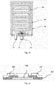
- an electrochromic grating as the out-cell device will be illustrated as an example as follows. As shown in Figure 4a , the electrochromic grating comprises two transparent comb-like electrodes 201 and 202 that form an interdigitated structure, and an electrochromic material 203 filled in gaps between the two comb-like electrodes. Specifically, two ends P1 and P2 of the two separate comb-like electrodes may serve as third lead terminals of the out-cell device.
- Conduction between the out-cell device and the external signal is realized by electrically connecting the third lead terminals to the second leads of the display device via the conductive glue.
- An electric field is formed between the comb-like electrodes by applying positive and negative voltage signals to the two ends P1 and P2 of the two separate comb-like electrodes, such that the electrochromic material filled in gaps between the two comb-like electrodes can change its color under the effect of the electric field, thereby enabling display of different colors and finally achieving the normal display function of the electrochromic grating.
- the electrochromic grating may also be the laminated structure as shown in Figure 4b , wherein the electrochromic grating comprises a first transparent electrode 204 and a second transparent electrode 205, and an electrochromic material 203 filled between the two transparent electrodes.
- Two ends P3 and P4 of the two separate transparent electrodes may serve as third lead ends of the out-cell device. Electrically connecting the third lead ends to the second leads of the display device via a conductive glue enables conduction between the out-cell device and the external signal.
- FIG. 4c shows a cross-sectional diagram of the transparent electrode layers of a laminated structure along the cut direction AB as shown in Figure 4b .
- the embodiments of the present invention provide a method for manufacturing the aforesaid display apparatus.
- the out-cell device is an auxiliary device for three-dimensional display, a touch control device or an electrochromic device. As shown in Figure 5 , the method may specifically comprise the steps of:
- first leads and second leads are set in the binding area of the display device; third leads are set in the binding area of the out-cell device; the third leads of the out-cell device are electrically connected to the second leads of the display device the electrical connection is realized using a conductive glue); the first leads of the display device are electrically connected to the first pins of the flexible printed circuit board; and the second leads of the display device are electrically connected to the second pins of the flexible printed circuit board.
- the third leads of the out-cell device are electrically connected to the second leads of the display device via the conductive glue, while the second leads are electrically connected to the second pins of the flexible printed circuit board, thereby realizing conduction between the out-cell device and the external signal.
- the display apparatus as provided in the embodiments of the present invention omits the step of separately making a flexible printed circuit board of the out-cell device, thereby reducing the cost of production of the display apparatus and at the same time further simplifying the structure of the out-cell device of the display apparatus.
- covering a layer of protective glue on the conductive glue can prevent the conductive glue from falling off by accident due to direct contact during the processes of manufacturing the display apparatus, thereby ensuring the electrical connection between the third leads of the out-cell device and the second leads of the display device and thus ensuring conduction between the out-cell device and the external signal.
- the embodiments of the present invention provide a display apparatus and a manufacturing method thereof.
- the display apparatus comprises a display device, an out-cell device and a flexible printed circuit board for being connected to an external signal; wherein a binding area of the display device has first leads and second leads; a binding area of the out-cell device has third leads, and the third leads are electrically connected to the second leads; and the flexible printed circuit board has first pins and second pins, the first leads are electrically connected to the first pins, and the second leads are electrically connected to the second pins.
- the third leads are electrically connected to the second leads via a conductive glue, and the conductive glue is further covered with a layer of protective glue.
- the third leads of the out-cell device are electrically connected to the second leads of the display device, while the second leads are electrically connected to the second pins of the flexible printed circuit board, thereby enabling conduction between the out-cell device and the external signal.
- the display apparatus as provided in the embodiments of the present invention omits the step of separately making a flexible printed circuit board of the out-cell device, thereby reducing the cost of production of the display apparatus and at the same time further simplifying the structure of the out-cell device of the display apparatus.
- Covering a layer of protective glue on the conductive glue can prevent the conductive glue from falling off by accident due to direct contact during the processes of manufacturing the display apparatus, thereby ensuring the electrical connection between the third leads of the out-cell device and the second leads of the display device and thus ensuring conduction between the out-cell device and the external signal.
Landscapes
- Physics & Mathematics (AREA)
- Nonlinear Science (AREA)
- General Physics & Mathematics (AREA)
- Engineering & Computer Science (AREA)
- Optics & Photonics (AREA)
- Mathematical Physics (AREA)
- Chemical & Material Sciences (AREA)
- Crystallography & Structural Chemistry (AREA)
- Theoretical Computer Science (AREA)
- General Engineering & Computer Science (AREA)
- Signal Processing (AREA)
- Multimedia (AREA)
- Human Computer Interaction (AREA)
- Computer Networks & Wireless Communication (AREA)
- Devices For Indicating Variable Information By Combining Individual Elements (AREA)
- Electrochromic Elements, Electrophoresis, Or Variable Reflection Or Absorption Elements (AREA)
- Liquid Crystal (AREA)
Claims (6)
- Anzeigevorrichtung, umfassend eine Anzeigeeinrichtung (1), eine Ausgangszelleneinrichtung (2) und eine flexible Leiterplatte (3), die dazu angepasst ist, mit einem externen Signal verbunden zu werden, wobei die Ausgangszelleneinrichtung (2) eine Hilfseinrichtung zur Realisierung eines dreidimensionalen Anzeigeeffekts, eine Berührungssteuereinrichtung oder eine elektrochrome Einrichtung ist;ein Bindebereich der Anzeigeeinrichtung (1) erste Leitungen (L1) und zweite Leitungen (L2) aufweist;ein Bindungsbereich der Ausgangszelleneinrichtung (2) dritte Leitungen aufweist, wobei die dritten Leitungen elektrisch mit den zweiten Leitungen (L2) verbunden sind;die flexible Leiterplatte (3) erste Stifte und zweite Stifte aufweist, wobei die ersten Leitungen (L1) elektrisch mit den ersten Stiften verbunden sind und die zweiten Leitungen (L2) elektrisch mit den zweiten Stiften verbunden sind; und dadurch gekennzeichnet, dassdie dritten Leitungen mit den zweiten Leitungen (L2) über einen leitfähigen Klebstoff (D1) elektrisch verbunden sind,der leitfähige Klebstoff (D1) ferner mit einer Schicht Schutzklebstoff (D2) bedeckt ist.
- Anzeigevorrichtung gemäß Anspruch 1, wobei der leitfähige Klebstoff (D1) ein Silberklebstoff ist.
- Anzeigevorrichtung gemäß Anspruch 1, wobei in dem Bindungsbereich der Anzeigeeinrichtung (1) die ersten Leitungen (L1) und die zweiten Leitungen (L2) parallel angeordnet sind und die zweiten Leitungen (L2) an zwei Seiten oder einer Seite der ersten Leitungen (L1) angeordnet sind.
- Anzeigevorrichtung gemäß Anspruch 1, wobei die Hilfseinrichtung zur Realisierung eines dreidimensionalen Anzeigeeffekts eine Flüssigkristallbarriere, ein elektrochromes Gitter oder eine Flüssigkristalllinse ist.
- Anzeigevorrichtung gemäß Anspruch 1, wobei die Ausgangszelleneinrichtung (2) eine transparente Elektrode (201, 202, 204, 205) umfasst, wobei die transparente Elektrode (201, 202, 204, 205) eine interdigitale Struktur oder eine laminierte Struktur ist.
- Verfahren zur Herstellung der Anzeigeeinrichtung gemäß einem der Ansprüche 1 bis 5, wobei das Verfahren umfasst:Bilden von ersten Leitungen (L1) und zweiten Leitungen (L2) im Bindungsbereich der Anzeigeeinrichtung (1);Bilden von dritten Leitungen im Bindungsbereich der Ausgangszelleneinrichtung (2);elektrisches Verbinden der dritten Leitungen der Ausgangszelleneinrichtung (2) mit den zweiten Leitungen (L2) der Anzeigeeinrichtung (1) mittels eines leitfähigen Klebstoffs (D1);elektrisches Verbinden der ersten Leitungen (L1) der Anzeigeeinrichtung (1) mit den ersten Stiften der flexiblen Leiterplatte (3) und elektrisches Verbinden der zweiten Leitungen (L2) der Anzeigeeinrichtung (1) mit den zweiten Stiften der flexiblen Leiterplatte (3); wobeinach dem elektrischen Verbinden der dritten Leitungen der Ausgangszelleneinrichtung (2) mit den zweiten Leitungen (L2) der Anzeigeeinrichtung (1) mittels eines leitfähigen Klebstoffs (D1) Beschichten des leitfähigen Klebstoffs (D1) mit einer Schicht aus Schutzklebstoff (D2) .
Applications Claiming Priority (2)
| Application Number | Priority Date | Filing Date | Title |
|---|---|---|---|
| CN201510064932.7A CN104570518A (zh) | 2015-02-06 | 2015-02-06 | 一种显示装置及其制作方法 |
| PCT/CN2015/084238 WO2016123911A1 (zh) | 2015-02-06 | 2015-07-16 | 一种显示装置及其制作方法 |
Publications (3)
| Publication Number | Publication Date |
|---|---|
| EP3255487A1 EP3255487A1 (de) | 2017-12-13 |
| EP3255487A4 EP3255487A4 (de) | 2018-08-08 |
| EP3255487B1 true EP3255487B1 (de) | 2021-10-20 |
Family
ID=53086969
Family Applications (1)
| Application Number | Title | Priority Date | Filing Date |
|---|---|---|---|
| EP15880864.2A Active EP3255487B1 (de) | 2015-02-06 | 2015-07-16 | Anzeigevorrichtung und herstellungsverfahren dafür |
Country Status (4)
| Country | Link |
|---|---|
| US (1) | US9946136B2 (de) |
| EP (1) | EP3255487B1 (de) |
| CN (1) | CN104570518A (de) |
| WO (1) | WO2016123911A1 (de) |
Families Citing this family (5)
| Publication number | Priority date | Publication date | Assignee | Title |
|---|---|---|---|---|
| CN104570518A (zh) | 2015-02-06 | 2015-04-29 | 京东方科技集团股份有限公司 | 一种显示装置及其制作方法 |
| JP2017044829A (ja) * | 2015-08-26 | 2017-03-02 | 三菱電機株式会社 | 液晶表示装置 |
| CN106773446A (zh) * | 2017-01-18 | 2017-05-31 | 张家港康得新光电材料有限公司 | 显示装置 |
| CN109597508A (zh) * | 2017-09-30 | 2019-04-09 | 南昌欧菲显示科技有限公司 | 柔性电路板、触控模组及触摸屏 |
| CN110047804B (zh) * | 2019-04-30 | 2021-08-03 | 京东方科技集团股份有限公司 | 阵列基板及制作方法、显示面板、拼接屏 |
Citations (2)
| Publication number | Priority date | Publication date | Assignee | Title |
|---|---|---|---|---|
| JP2009199107A (ja) * | 2008-02-19 | 2009-09-03 | Mitsubishi Electric Corp | タッチパネル付き表示装置 |
| US20140375907A1 (en) * | 2013-06-20 | 2014-12-25 | Gio Optoelectronics Corp. | Touch display panel and touch display apparatus |
Family Cites Families (20)
| Publication number | Priority date | Publication date | Assignee | Title |
|---|---|---|---|---|
| FR2618571B1 (fr) * | 1987-07-24 | 1990-10-19 | Warszawski Bernard | Materiau pour la modulation de la lumiere et procedes de fabrication |
| KR100637303B1 (ko) * | 2002-09-26 | 2006-10-24 | 샤프 가부시키가이샤 | 2d/3d 전환형 액정 표시 패널, 및 2d/3d 전환형 액정표시 장치 |
| US9710095B2 (en) * | 2007-01-05 | 2017-07-18 | Apple Inc. | Touch screen stack-ups |
| JP2009116090A (ja) * | 2007-11-07 | 2009-05-28 | Hitachi Displays Ltd | 液晶表示装置 |
| US8044330B2 (en) * | 2008-01-17 | 2011-10-25 | E.I. Du Pont De Nemours And Company | Electrically conductive adhesive |
| JP5224242B2 (ja) * | 2008-04-09 | 2013-07-03 | Nltテクノロジー株式会社 | 表示装置、液晶表示装置、電子機器、及び表示装置用製造方法 |
| DE112009003123B4 (de) * | 2008-12-11 | 2020-02-06 | Osram Oled Gmbh | Organische leuchtdiode und beleuchtungsmittel |
| JP5294883B2 (ja) * | 2009-01-05 | 2013-09-18 | 株式会社ジャパンディスプレイウェスト | 液晶表示装置および電子機器 |
| JP2011095451A (ja) * | 2009-10-29 | 2011-05-12 | Sony Corp | 横電界方式の液晶表示装置 |
| US8823668B2 (en) * | 2009-12-08 | 2014-09-02 | Sharp Kabushiki Kaisha | Liquid crystal device |
| TW201205384A (en) * | 2010-06-04 | 2012-02-01 | Wintek Corp | Touch-sensitive device and fabrication method thereof |
| KR101319347B1 (ko) * | 2010-06-10 | 2013-10-16 | 엘지디스플레이 주식회사 | 터치 패널 일체형 액정 표시 장치 |
| KR101756656B1 (ko) * | 2010-06-25 | 2017-07-11 | 엘지디스플레이 주식회사 | 터치 패널 내장형 유기발광다이오드 표시 장치 |
| JP2013182186A (ja) * | 2012-03-02 | 2013-09-12 | Japan Display West Co Ltd | 表示装置、電子機器および貼り合わせ構造 |
| CN102695364B (zh) * | 2012-05-30 | 2018-05-01 | 固安翌光科技有限公司 | Oled光源用fpc、oled光源及oled光源引出电极的连接方法 |
| CN103904096B (zh) * | 2012-12-27 | 2018-02-27 | 上海天马微电子有限公司 | 双面oled显示面板及制造方法 |
| CN103116233B (zh) * | 2013-01-23 | 2016-01-06 | 北京京东方光电科技有限公司 | 一种触摸液晶光栅结构及3d触摸显示装置 |
| CN103926736B (zh) * | 2013-12-23 | 2017-06-06 | 上海天马微电子有限公司 | 一种彩膜基板以及触摸屏显示装置 |
| CN104049802A (zh) * | 2014-06-06 | 2014-09-17 | 深圳莱宝高科技股份有限公司 | 触控显示装置 |
| CN104570518A (zh) * | 2015-02-06 | 2015-04-29 | 京东方科技集团股份有限公司 | 一种显示装置及其制作方法 |
-
2015
- 2015-02-06 CN CN201510064932.7A patent/CN104570518A/zh active Pending
- 2015-07-16 US US14/906,503 patent/US9946136B2/en active Active
- 2015-07-16 EP EP15880864.2A patent/EP3255487B1/de active Active
- 2015-07-16 WO PCT/CN2015/084238 patent/WO2016123911A1/zh not_active Ceased
Patent Citations (2)
| Publication number | Priority date | Publication date | Assignee | Title |
|---|---|---|---|---|
| JP2009199107A (ja) * | 2008-02-19 | 2009-09-03 | Mitsubishi Electric Corp | タッチパネル付き表示装置 |
| US20140375907A1 (en) * | 2013-06-20 | 2014-12-25 | Gio Optoelectronics Corp. | Touch display panel and touch display apparatus |
Also Published As
| Publication number | Publication date |
|---|---|
| US20160370683A1 (en) | 2016-12-22 |
| WO2016123911A1 (zh) | 2016-08-11 |
| CN104570518A (zh) | 2015-04-29 |
| US9946136B2 (en) | 2018-04-17 |
| EP3255487A4 (de) | 2018-08-08 |
| EP3255487A1 (de) | 2017-12-13 |
Similar Documents
| Publication | Publication Date | Title |
|---|---|---|
| CN105717682B (zh) | 一种触控显示装置 | |
| EP2946643B1 (de) | Verfahren und vorrichtung zur kopplung eines aktiven anzeigeteils und substrats | |
| US8754332B2 (en) | Display device | |
| US11543719B2 (en) | Light control unit | |
| EP3255487B1 (de) | Anzeigevorrichtung und herstellungsverfahren dafür | |
| CN108469927B (zh) | 触控显示面板及其驱动方法、触控显示装置 | |
| TWI526905B (zh) | 觸控面板模組與具有觸控面板模組的觸控顯示裝置 | |
| US20150022741A1 (en) | Display device, electronic device, and touch panel | |
| CN109188747B (zh) | 显示面板和显示装置 | |
| CN108363510B (zh) | 触控显示屏及其制备方法和电子产品 | |
| CN102073161A (zh) | 可切换式立体显示器 | |
| CN106445230A (zh) | 一种触控面板及其制备方法、显示装置 | |
| US20180373091A1 (en) | Display panel | |
| CN108803111B (zh) | 显示面板、显示装置和显示面板的制作方法 | |
| EP4286933B1 (de) | Elektrochromes bauelement und elektronische vorrichtung | |
| CN105912167A (zh) | 一种触控模组及其制作方法、显示面板和显示装置 | |
| CN107368216B (zh) | 触控面板及显示设备 | |
| CN113867575B (zh) | 触控显示面板、显示装置及制作方法 | |
| US7746662B2 (en) | Touch panel | |
| CN104731414B (zh) | 触控显示装置及电子设备 | |
| CN106843611A (zh) | 导电膜及触摸屏 | |
| CN107368217B (zh) | 触控面板及显示设备 | |
| CN112449486B (zh) | 显示设备 | |
| CN205507292U (zh) | 一种触控显示装置 | |
| CN203606592U (zh) | 一种液晶显示模组和液晶显示装置 |
Legal Events
| Date | Code | Title | Description |
|---|---|---|---|
| STAA | Information on the status of an ep patent application or granted ep patent |
Free format text: STATUS: THE INTERNATIONAL PUBLICATION HAS BEEN MADE |
|
| PUAI | Public reference made under article 153(3) epc to a published international application that has entered the european phase |
Free format text: ORIGINAL CODE: 0009012 |
|
| STAA | Information on the status of an ep patent application or granted ep patent |
Free format text: STATUS: REQUEST FOR EXAMINATION WAS MADE |
|
| 17P | Request for examination filed |
Effective date: 20170116 |
|
| AK | Designated contracting states |
Kind code of ref document: A1 Designated state(s): AL AT BE BG CH CY CZ DE DK EE ES FI FR GB GR HR HU IE IS IT LI LT LU LV MC MK MT NL NO PL PT RO RS SE SI SK SM TR |
|
| AX | Request for extension of the european patent |
Extension state: BA ME |
|
| DAV | Request for validation of the european patent (deleted) | ||
| DAX | Request for extension of the european patent (deleted) | ||
| REG | Reference to a national code |
Ref country code: DE Ref legal event code: R079 Ref document number: 602015074365 Country of ref document: DE Free format text: PREVIOUS MAIN CLASS: G02F0001134300 Ipc: G02F0001133300 |
|
| A4 | Supplementary search report drawn up and despatched |
Effective date: 20180710 |
|
| RIC1 | Information provided on ipc code assigned before grant |
Ipc: H05K 1/11 20060101ALN20180703BHEP Ipc: H01R 12/00 20060101ALN20180703BHEP Ipc: G02B 27/00 20060101ALN20180703BHEP Ipc: G02F 1/1333 20060101AFI20180703BHEP Ipc: H05K 3/32 20060101ALN20180703BHEP Ipc: G02F 1/1345 20060101ALI20180703BHEP Ipc: H04N 13/00 20060101ALN20180703BHEP Ipc: G06F 3/041 20060101ALI20180703BHEP Ipc: H01R 12/50 20110101ALN20180703BHEP |
|
| STAA | Information on the status of an ep patent application or granted ep patent |
Free format text: STATUS: EXAMINATION IS IN PROGRESS |
|
| 17Q | First examination report despatched |
Effective date: 20200925 |
|
| GRAP | Despatch of communication of intention to grant a patent |
Free format text: ORIGINAL CODE: EPIDOSNIGR1 |
|
| STAA | Information on the status of an ep patent application or granted ep patent |
Free format text: STATUS: GRANT OF PATENT IS INTENDED |
|
| INTG | Intention to grant announced |
Effective date: 20210428 |
|
| GRAS | Grant fee paid |
Free format text: ORIGINAL CODE: EPIDOSNIGR3 |
|
| GRAA | (expected) grant |
Free format text: ORIGINAL CODE: 0009210 |
|
| STAA | Information on the status of an ep patent application or granted ep patent |
Free format text: STATUS: THE PATENT HAS BEEN GRANTED |
|
| AK | Designated contracting states |
Kind code of ref document: B1 Designated state(s): AL AT BE BG CH CY CZ DE DK EE ES FI FR GB GR HR HU IE IS IT LI LT LU LV MC MK MT NL NO PL PT RO RS SE SI SK SM TR |
|
| REG | Reference to a national code |
Ref country code: GB Ref legal event code: FG4D |
|
| REG | Reference to a national code |
Ref country code: CH Ref legal event code: EP |
|
| REG | Reference to a national code |
Ref country code: IE Ref legal event code: FG4D |
|
| REG | Reference to a national code |
Ref country code: DE Ref legal event code: R096 Ref document number: 602015074365 Country of ref document: DE |
|
| REG | Reference to a national code |
Ref country code: AT Ref legal event code: REF Ref document number: 1440421 Country of ref document: AT Kind code of ref document: T Effective date: 20211115 |
|
| REG | Reference to a national code |
Ref country code: LT Ref legal event code: MG9D |
|
| REG | Reference to a national code |
Ref country code: NL Ref legal event code: MP Effective date: 20211020 |
|
| REG | Reference to a national code |
Ref country code: AT Ref legal event code: MK05 Ref document number: 1440421 Country of ref document: AT Kind code of ref document: T Effective date: 20211020 |
|
| PG25 | Lapsed in a contracting state [announced via postgrant information from national office to epo] |
Ref country code: RS Free format text: LAPSE BECAUSE OF FAILURE TO SUBMIT A TRANSLATION OF THE DESCRIPTION OR TO PAY THE FEE WITHIN THE PRESCRIBED TIME-LIMIT Effective date: 20211020 Ref country code: LT Free format text: LAPSE BECAUSE OF FAILURE TO SUBMIT A TRANSLATION OF THE DESCRIPTION OR TO PAY THE FEE WITHIN THE PRESCRIBED TIME-LIMIT Effective date: 20211020 Ref country code: FI Free format text: LAPSE BECAUSE OF FAILURE TO SUBMIT A TRANSLATION OF THE DESCRIPTION OR TO PAY THE FEE WITHIN THE PRESCRIBED TIME-LIMIT Effective date: 20211020 Ref country code: BG Free format text: LAPSE BECAUSE OF FAILURE TO SUBMIT A TRANSLATION OF THE DESCRIPTION OR TO PAY THE FEE WITHIN THE PRESCRIBED TIME-LIMIT Effective date: 20220120 Ref country code: AT Free format text: LAPSE BECAUSE OF FAILURE TO SUBMIT A TRANSLATION OF THE DESCRIPTION OR TO PAY THE FEE WITHIN THE PRESCRIBED TIME-LIMIT Effective date: 20211020 |
|
| PG25 | Lapsed in a contracting state [announced via postgrant information from national office to epo] |
Ref country code: IS Free format text: LAPSE BECAUSE OF FAILURE TO SUBMIT A TRANSLATION OF THE DESCRIPTION OR TO PAY THE FEE WITHIN THE PRESCRIBED TIME-LIMIT Effective date: 20220220 Ref country code: SE Free format text: LAPSE BECAUSE OF FAILURE TO SUBMIT A TRANSLATION OF THE DESCRIPTION OR TO PAY THE FEE WITHIN THE PRESCRIBED TIME-LIMIT Effective date: 20211020 Ref country code: PT Free format text: LAPSE BECAUSE OF FAILURE TO SUBMIT A TRANSLATION OF THE DESCRIPTION OR TO PAY THE FEE WITHIN THE PRESCRIBED TIME-LIMIT Effective date: 20220221 Ref country code: PL Free format text: LAPSE BECAUSE OF FAILURE TO SUBMIT A TRANSLATION OF THE DESCRIPTION OR TO PAY THE FEE WITHIN THE PRESCRIBED TIME-LIMIT Effective date: 20211020 Ref country code: NO Free format text: LAPSE BECAUSE OF FAILURE TO SUBMIT A TRANSLATION OF THE DESCRIPTION OR TO PAY THE FEE WITHIN THE PRESCRIBED TIME-LIMIT Effective date: 20220120 Ref country code: NL Free format text: LAPSE BECAUSE OF FAILURE TO SUBMIT A TRANSLATION OF THE DESCRIPTION OR TO PAY THE FEE WITHIN THE PRESCRIBED TIME-LIMIT Effective date: 20211020 Ref country code: LV Free format text: LAPSE BECAUSE OF FAILURE TO SUBMIT A TRANSLATION OF THE DESCRIPTION OR TO PAY THE FEE WITHIN THE PRESCRIBED TIME-LIMIT Effective date: 20211020 Ref country code: HR Free format text: LAPSE BECAUSE OF FAILURE TO SUBMIT A TRANSLATION OF THE DESCRIPTION OR TO PAY THE FEE WITHIN THE PRESCRIBED TIME-LIMIT Effective date: 20211020 Ref country code: GR Free format text: LAPSE BECAUSE OF FAILURE TO SUBMIT A TRANSLATION OF THE DESCRIPTION OR TO PAY THE FEE WITHIN THE PRESCRIBED TIME-LIMIT Effective date: 20220121 Ref country code: ES Free format text: LAPSE BECAUSE OF FAILURE TO SUBMIT A TRANSLATION OF THE DESCRIPTION OR TO PAY THE FEE WITHIN THE PRESCRIBED TIME-LIMIT Effective date: 20211020 |
|
| REG | Reference to a national code |
Ref country code: DE Ref legal event code: R097 Ref document number: 602015074365 Country of ref document: DE |
|
| PG25 | Lapsed in a contracting state [announced via postgrant information from national office to epo] |
Ref country code: SM Free format text: LAPSE BECAUSE OF FAILURE TO SUBMIT A TRANSLATION OF THE DESCRIPTION OR TO PAY THE FEE WITHIN THE PRESCRIBED TIME-LIMIT Effective date: 20211020 Ref country code: SK Free format text: LAPSE BECAUSE OF FAILURE TO SUBMIT A TRANSLATION OF THE DESCRIPTION OR TO PAY THE FEE WITHIN THE PRESCRIBED TIME-LIMIT Effective date: 20211020 Ref country code: RO Free format text: LAPSE BECAUSE OF FAILURE TO SUBMIT A TRANSLATION OF THE DESCRIPTION OR TO PAY THE FEE WITHIN THE PRESCRIBED TIME-LIMIT Effective date: 20211020 Ref country code: EE Free format text: LAPSE BECAUSE OF FAILURE TO SUBMIT A TRANSLATION OF THE DESCRIPTION OR TO PAY THE FEE WITHIN THE PRESCRIBED TIME-LIMIT Effective date: 20211020 Ref country code: DK Free format text: LAPSE BECAUSE OF FAILURE TO SUBMIT A TRANSLATION OF THE DESCRIPTION OR TO PAY THE FEE WITHIN THE PRESCRIBED TIME-LIMIT Effective date: 20211020 Ref country code: CZ Free format text: LAPSE BECAUSE OF FAILURE TO SUBMIT A TRANSLATION OF THE DESCRIPTION OR TO PAY THE FEE WITHIN THE PRESCRIBED TIME-LIMIT Effective date: 20211020 |
|
| PLBE | No opposition filed within time limit |
Free format text: ORIGINAL CODE: 0009261 |
|
| STAA | Information on the status of an ep patent application or granted ep patent |
Free format text: STATUS: NO OPPOSITION FILED WITHIN TIME LIMIT |
|
| 26N | No opposition filed |
Effective date: 20220721 |
|
| PG25 | Lapsed in a contracting state [announced via postgrant information from national office to epo] |
Ref country code: AL Free format text: LAPSE BECAUSE OF FAILURE TO SUBMIT A TRANSLATION OF THE DESCRIPTION OR TO PAY THE FEE WITHIN THE PRESCRIBED TIME-LIMIT Effective date: 20211020 |
|
| PG25 | Lapsed in a contracting state [announced via postgrant information from national office to epo] |
Ref country code: SI Free format text: LAPSE BECAUSE OF FAILURE TO SUBMIT A TRANSLATION OF THE DESCRIPTION OR TO PAY THE FEE WITHIN THE PRESCRIBED TIME-LIMIT Effective date: 20211020 |
|
| PG25 | Lapsed in a contracting state [announced via postgrant information from national office to epo] |
Ref country code: MC Free format text: LAPSE BECAUSE OF FAILURE TO SUBMIT A TRANSLATION OF THE DESCRIPTION OR TO PAY THE FEE WITHIN THE PRESCRIBED TIME-LIMIT Effective date: 20211020 |
|
| REG | Reference to a national code |
Ref country code: CH Ref legal event code: PL |
|
| GBPC | Gb: european patent ceased through non-payment of renewal fee |
Effective date: 20220716 |
|
| REG | Reference to a national code |
Ref country code: BE Ref legal event code: MM Effective date: 20220731 |
|
| PG25 | Lapsed in a contracting state [announced via postgrant information from national office to epo] |
Ref country code: LU Free format text: LAPSE BECAUSE OF NON-PAYMENT OF DUE FEES Effective date: 20220716 Ref country code: LI Free format text: LAPSE BECAUSE OF NON-PAYMENT OF DUE FEES Effective date: 20220731 Ref country code: FR Free format text: LAPSE BECAUSE OF NON-PAYMENT OF DUE FEES Effective date: 20220731 Ref country code: CH Free format text: LAPSE BECAUSE OF NON-PAYMENT OF DUE FEES Effective date: 20220731 |
|
| PG25 | Lapsed in a contracting state [announced via postgrant information from national office to epo] |
Ref country code: IT Free format text: LAPSE BECAUSE OF FAILURE TO SUBMIT A TRANSLATION OF THE DESCRIPTION OR TO PAY THE FEE WITHIN THE PRESCRIBED TIME-LIMIT Effective date: 20211020 Ref country code: GB Free format text: LAPSE BECAUSE OF NON-PAYMENT OF DUE FEES Effective date: 20220716 Ref country code: BE Free format text: LAPSE BECAUSE OF NON-PAYMENT OF DUE FEES Effective date: 20220731 |
|
| PG25 | Lapsed in a contracting state [announced via postgrant information from national office to epo] |
Ref country code: IE Free format text: LAPSE BECAUSE OF NON-PAYMENT OF DUE FEES Effective date: 20220716 |
|
| PG25 | Lapsed in a contracting state [announced via postgrant information from national office to epo] |
Ref country code: HU Free format text: LAPSE BECAUSE OF FAILURE TO SUBMIT A TRANSLATION OF THE DESCRIPTION OR TO PAY THE FEE WITHIN THE PRESCRIBED TIME-LIMIT; INVALID AB INITIO Effective date: 20150716 |
|
| PG25 | Lapsed in a contracting state [announced via postgrant information from national office to epo] |
Ref country code: MK Free format text: LAPSE BECAUSE OF FAILURE TO SUBMIT A TRANSLATION OF THE DESCRIPTION OR TO PAY THE FEE WITHIN THE PRESCRIBED TIME-LIMIT Effective date: 20211020 Ref country code: CY Free format text: LAPSE BECAUSE OF FAILURE TO SUBMIT A TRANSLATION OF THE DESCRIPTION OR TO PAY THE FEE WITHIN THE PRESCRIBED TIME-LIMIT Effective date: 20211020 |
|
| PG25 | Lapsed in a contracting state [announced via postgrant information from national office to epo] |
Ref country code: TR Free format text: LAPSE BECAUSE OF FAILURE TO SUBMIT A TRANSLATION OF THE DESCRIPTION OR TO PAY THE FEE WITHIN THE PRESCRIBED TIME-LIMIT Effective date: 20211020 |
|
| PG25 | Lapsed in a contracting state [announced via postgrant information from national office to epo] |
Ref country code: MT Free format text: LAPSE BECAUSE OF FAILURE TO SUBMIT A TRANSLATION OF THE DESCRIPTION OR TO PAY THE FEE WITHIN THE PRESCRIBED TIME-LIMIT Effective date: 20211020 |
|
| PGFP | Annual fee paid to national office [announced via postgrant information from national office to epo] |
Ref country code: DE Payment date: 20250728 Year of fee payment: 11 |