EP3255486A1 - Anzeigevorrichtung - Google Patents
Anzeigevorrichtung Download PDFInfo
- Publication number
- EP3255486A1 EP3255486A1 EP15837077.5A EP15837077A EP3255486A1 EP 3255486 A1 EP3255486 A1 EP 3255486A1 EP 15837077 A EP15837077 A EP 15837077A EP 3255486 A1 EP3255486 A1 EP 3255486A1
- Authority
- EP
- European Patent Office
- Prior art keywords
- display panel
- light incoming
- light
- array substrate
- edge
- Prior art date
- Legal status (The legal status is an assumption and is not a legal conclusion. Google has not performed a legal analysis and makes no representation as to the accuracy of the status listed.)
- Granted
Links
Images

Classifications
-
- G—PHYSICS
- G02—OPTICS
- G02F—OPTICAL DEVICES OR ARRANGEMENTS FOR THE CONTROL OF LIGHT BY MODIFICATION OF THE OPTICAL PROPERTIES OF THE MEDIA OF THE ELEMENTS INVOLVED THEREIN; NON-LINEAR OPTICS; FREQUENCY-CHANGING OF LIGHT; OPTICAL LOGIC ELEMENTS; OPTICAL ANALOGUE/DIGITAL CONVERTERS
- G02F1/00—Devices or arrangements for the control of the intensity, colour, phase, polarisation or direction of light arriving from an independent light source, e.g. switching, gating or modulating; Non-linear optics
- G02F1/01—Devices or arrangements for the control of the intensity, colour, phase, polarisation or direction of light arriving from an independent light source, e.g. switching, gating or modulating; Non-linear optics for the control of the intensity, phase, polarisation or colour
- G02F1/13—Devices or arrangements for the control of the intensity, colour, phase, polarisation or direction of light arriving from an independent light source, e.g. switching, gating or modulating; Non-linear optics for the control of the intensity, phase, polarisation or colour based on liquid crystals, e.g. single liquid crystal display cells
- G02F1/133—Constructional arrangements; Operation of liquid crystal cells; Circuit arrangements
- G02F1/1333—Constructional arrangements; Manufacturing methods
- G02F1/1335—Structural association of cells with optical devices, e.g. polarisers or reflectors
- G02F1/1336—Illuminating devices
- G02F1/133615—Edge-illuminating devices, i.e. illuminating from the side
-
- G—PHYSICS
- G02—OPTICS
- G02F—OPTICAL DEVICES OR ARRANGEMENTS FOR THE CONTROL OF LIGHT BY MODIFICATION OF THE OPTICAL PROPERTIES OF THE MEDIA OF THE ELEMENTS INVOLVED THEREIN; NON-LINEAR OPTICS; FREQUENCY-CHANGING OF LIGHT; OPTICAL LOGIC ELEMENTS; OPTICAL ANALOGUE/DIGITAL CONVERTERS
- G02F1/00—Devices or arrangements for the control of the intensity, colour, phase, polarisation or direction of light arriving from an independent light source, e.g. switching, gating or modulating; Non-linear optics
- G02F1/01—Devices or arrangements for the control of the intensity, colour, phase, polarisation or direction of light arriving from an independent light source, e.g. switching, gating or modulating; Non-linear optics for the control of the intensity, phase, polarisation or colour
- G02F1/13—Devices or arrangements for the control of the intensity, colour, phase, polarisation or direction of light arriving from an independent light source, e.g. switching, gating or modulating; Non-linear optics for the control of the intensity, phase, polarisation or colour based on liquid crystals, e.g. single liquid crystal display cells
- G02F1/133—Constructional arrangements; Operation of liquid crystal cells; Circuit arrangements
- G02F1/1333—Constructional arrangements; Manufacturing methods
- G02F1/1335—Structural association of cells with optical devices, e.g. polarisers or reflectors
- G02F1/133509—Filters, e.g. light shielding masks
- G02F1/133512—Light shielding layers, e.g. black matrix
-
- G—PHYSICS
- G02—OPTICS
- G02B—OPTICAL ELEMENTS, SYSTEMS OR APPARATUS
- G02B6/00—Light guides; Structural details of arrangements comprising light guides and other optical elements, e.g. couplings
- G02B6/0001—Light guides; Structural details of arrangements comprising light guides and other optical elements, e.g. couplings specially adapted for lighting devices or systems
- G02B6/0011—Light guides; Structural details of arrangements comprising light guides and other optical elements, e.g. couplings specially adapted for lighting devices or systems the light guides being planar or of plate-like form
- G02B6/0033—Means for improving the coupling-out of light from the light guide
- G02B6/005—Means for improving the coupling-out of light from the light guide provided by one optical element, or plurality thereof, placed on the light output side of the light guide
- G02B6/0053—Prismatic sheet or layer; Brightness enhancement element, sheet or layer
-
- G—PHYSICS
- G02—OPTICS
- G02B—OPTICAL ELEMENTS, SYSTEMS OR APPARATUS
- G02B6/00—Light guides; Structural details of arrangements comprising light guides and other optical elements, e.g. couplings
- G02B6/0001—Light guides; Structural details of arrangements comprising light guides and other optical elements, e.g. couplings specially adapted for lighting devices or systems
- G02B6/0011—Light guides; Structural details of arrangements comprising light guides and other optical elements, e.g. couplings specially adapted for lighting devices or systems the light guides being planar or of plate-like form
- G02B6/0033—Means for improving the coupling-out of light from the light guide
- G02B6/0056—Means for improving the coupling-out of light from the light guide for producing polarisation effects, e.g. by a surface with polarizing properties or by an additional polarizing elements
-
- G—PHYSICS
- G02—OPTICS
- G02B—OPTICAL ELEMENTS, SYSTEMS OR APPARATUS
- G02B6/00—Light guides; Structural details of arrangements comprising light guides and other optical elements, e.g. couplings
- G02B6/0001—Light guides; Structural details of arrangements comprising light guides and other optical elements, e.g. couplings specially adapted for lighting devices or systems
- G02B6/0011—Light guides; Structural details of arrangements comprising light guides and other optical elements, e.g. couplings specially adapted for lighting devices or systems the light guides being planar or of plate-like form
- G02B6/0066—Light guides; Structural details of arrangements comprising light guides and other optical elements, e.g. couplings specially adapted for lighting devices or systems the light guides being planar or of plate-like form characterised by the light source being coupled to the light guide
- G02B6/0068—Arrangements of plural sources, e.g. multi-colour light sources
-
- G—PHYSICS
- G02—OPTICS
- G02B—OPTICAL ELEMENTS, SYSTEMS OR APPARATUS
- G02B6/00—Light guides; Structural details of arrangements comprising light guides and other optical elements, e.g. couplings
- G02B6/0001—Light guides; Structural details of arrangements comprising light guides and other optical elements, e.g. couplings specially adapted for lighting devices or systems
- G02B6/0011—Light guides; Structural details of arrangements comprising light guides and other optical elements, e.g. couplings specially adapted for lighting devices or systems the light guides being planar or of plate-like form
- G02B6/0081—Mechanical or electrical aspects of the light guide and light source in the lighting device peculiar to the adaptation to planar light guides, e.g. concerning packaging
- G02B6/0086—Positioning aspects
- G02B6/0088—Positioning aspects of the light guide or other optical sheets in the package
-
- G—PHYSICS
- G02—OPTICS
- G02B—OPTICAL ELEMENTS, SYSTEMS OR APPARATUS
- G02B6/00—Light guides; Structural details of arrangements comprising light guides and other optical elements, e.g. couplings
- G02B6/0001—Light guides; Structural details of arrangements comprising light guides and other optical elements, e.g. couplings specially adapted for lighting devices or systems
- G02B6/0011—Light guides; Structural details of arrangements comprising light guides and other optical elements, e.g. couplings specially adapted for lighting devices or systems the light guides being planar or of plate-like form
- G02B6/0081—Mechanical or electrical aspects of the light guide and light source in the lighting device peculiar to the adaptation to planar light guides, e.g. concerning packaging
- G02B6/0093—Means for protecting the light guide
-
- G—PHYSICS
- G02—OPTICS
- G02F—OPTICAL DEVICES OR ARRANGEMENTS FOR THE CONTROL OF LIGHT BY MODIFICATION OF THE OPTICAL PROPERTIES OF THE MEDIA OF THE ELEMENTS INVOLVED THEREIN; NON-LINEAR OPTICS; FREQUENCY-CHANGING OF LIGHT; OPTICAL LOGIC ELEMENTS; OPTICAL ANALOGUE/DIGITAL CONVERTERS
- G02F1/00—Devices or arrangements for the control of the intensity, colour, phase, polarisation or direction of light arriving from an independent light source, e.g. switching, gating or modulating; Non-linear optics
- G02F1/01—Devices or arrangements for the control of the intensity, colour, phase, polarisation or direction of light arriving from an independent light source, e.g. switching, gating or modulating; Non-linear optics for the control of the intensity, phase, polarisation or colour
- G02F1/13—Devices or arrangements for the control of the intensity, colour, phase, polarisation or direction of light arriving from an independent light source, e.g. switching, gating or modulating; Non-linear optics for the control of the intensity, phase, polarisation or colour based on liquid crystals, e.g. single liquid crystal display cells
- G02F1/133—Constructional arrangements; Operation of liquid crystal cells; Circuit arrangements
- G02F1/1333—Constructional arrangements; Manufacturing methods
- G02F1/133308—Support structures for LCD panels, e.g. frames or bezels
-
- G—PHYSICS
- G02—OPTICS
- G02F—OPTICAL DEVICES OR ARRANGEMENTS FOR THE CONTROL OF LIGHT BY MODIFICATION OF THE OPTICAL PROPERTIES OF THE MEDIA OF THE ELEMENTS INVOLVED THEREIN; NON-LINEAR OPTICS; FREQUENCY-CHANGING OF LIGHT; OPTICAL LOGIC ELEMENTS; OPTICAL ANALOGUE/DIGITAL CONVERTERS
- G02F1/00—Devices or arrangements for the control of the intensity, colour, phase, polarisation or direction of light arriving from an independent light source, e.g. switching, gating or modulating; Non-linear optics
- G02F1/01—Devices or arrangements for the control of the intensity, colour, phase, polarisation or direction of light arriving from an independent light source, e.g. switching, gating or modulating; Non-linear optics for the control of the intensity, phase, polarisation or colour
- G02F1/13—Devices or arrangements for the control of the intensity, colour, phase, polarisation or direction of light arriving from an independent light source, e.g. switching, gating or modulating; Non-linear optics for the control of the intensity, phase, polarisation or colour based on liquid crystals, e.g. single liquid crystal display cells
- G02F1/133—Constructional arrangements; Operation of liquid crystal cells; Circuit arrangements
- G02F1/1333—Constructional arrangements; Manufacturing methods
- G02F1/1335—Structural association of cells with optical devices, e.g. polarisers or reflectors
- G02F1/1336—Illuminating devices
-
- G—PHYSICS
- G02—OPTICS
- G02F—OPTICAL DEVICES OR ARRANGEMENTS FOR THE CONTROL OF LIGHT BY MODIFICATION OF THE OPTICAL PROPERTIES OF THE MEDIA OF THE ELEMENTS INVOLVED THEREIN; NON-LINEAR OPTICS; FREQUENCY-CHANGING OF LIGHT; OPTICAL LOGIC ELEMENTS; OPTICAL ANALOGUE/DIGITAL CONVERTERS
- G02F1/00—Devices or arrangements for the control of the intensity, colour, phase, polarisation or direction of light arriving from an independent light source, e.g. switching, gating or modulating; Non-linear optics
- G02F1/01—Devices or arrangements for the control of the intensity, colour, phase, polarisation or direction of light arriving from an independent light source, e.g. switching, gating or modulating; Non-linear optics for the control of the intensity, phase, polarisation or colour
- G02F1/13—Devices or arrangements for the control of the intensity, colour, phase, polarisation or direction of light arriving from an independent light source, e.g. switching, gating or modulating; Non-linear optics for the control of the intensity, phase, polarisation or colour based on liquid crystals, e.g. single liquid crystal display cells
- G02F1/133—Constructional arrangements; Operation of liquid crystal cells; Circuit arrangements
- G02F1/1333—Constructional arrangements; Manufacturing methods
- G02F1/133308—Support structures for LCD panels, e.g. frames or bezels
- G02F1/133317—Intermediate frames, e.g. between backlight housing and front frame
-
- G—PHYSICS
- G02—OPTICS
- G02F—OPTICAL DEVICES OR ARRANGEMENTS FOR THE CONTROL OF LIGHT BY MODIFICATION OF THE OPTICAL PROPERTIES OF THE MEDIA OF THE ELEMENTS INVOLVED THEREIN; NON-LINEAR OPTICS; FREQUENCY-CHANGING OF LIGHT; OPTICAL LOGIC ELEMENTS; OPTICAL ANALOGUE/DIGITAL CONVERTERS
- G02F2201/00—Constructional arrangements not provided for in groups G02F1/00 - G02F7/00
- G02F2201/50—Protective arrangements
- G02F2201/503—Arrangements improving the resistance to shock
-
- G—PHYSICS
- G02—OPTICS
- G02F—OPTICAL DEVICES OR ARRANGEMENTS FOR THE CONTROL OF LIGHT BY MODIFICATION OF THE OPTICAL PROPERTIES OF THE MEDIA OF THE ELEMENTS INVOLVED THEREIN; NON-LINEAR OPTICS; FREQUENCY-CHANGING OF LIGHT; OPTICAL LOGIC ELEMENTS; OPTICAL ANALOGUE/DIGITAL CONVERTERS
- G02F2202/00—Materials and properties
- G02F2202/28—Adhesive materials or arrangements
Definitions
- the invention refers to a technical field of display, and specifically to a display device.
- a display device of intermediate or small size includes a display panel and a backlight module for providing light source for the display panel, which backlight module includes a back plate, a light guide plate and a light strip mounted in the back plate.
- the display panel is mounted on the back plate of the backlight module, and a shading tape disposed along the edges of the display panel is provided between the display panel and the back light module, for preventing light leakage defect from occurring in the display device.
- a side of the light guide plate that is provided with a light strip is a light incoming side
- an edge at which the side of the display panel's sides which is opposite to the light incoming side of the backlight module is a light incoming edge.
- An end of the light incoming edge forms a light incoming corner with an end of an edge
- the other end of the light incoming edge forms a light incoming corner with an end of another edge. Since the light intensity incoming from a side of the light incoming surface of the light guide plate is larger, for achieving good shading effect, the shading tape at the light incoming edge and the light incoming corner of the display panel has a larger width.
- the display panel is increasing thinner, and an extrusive stress easily occurs when the corner of the thinning display panel is stuck by large area, resulting in water ripple in the picture of the display panel. Therefore, a phenomenon of water ripple and light leakage easily occurs in a portion of the display panel which corresponds to the light incoming corner.
- the invention provides a display device, wherein a phenomenon of water ripple and light leakage does not easily occur in a portion of a display panel which corresponds to a light incoming corner.
- the invention provides the following technical solution:
- the shading tape provided at each light incoming corner, the shading tape provided at the main body of the light incoming edge, and the shading tape provided at the main body of the adjacent edge forming the light incoming corner with the light incoming edge are separate from each other, that is have a separated structure; and only the shading tape provided at the parts of the edges of the display panel except the light incoming corners is provided with an adhesive layer, that is, the side, which faces the display panel, of the shading tape provided at the light incoming corners is not provided with an adhesive layer, i.e. does not been stuck to the display panel, so the parts of the display panel which correspond to the light incoming corners would not create extrusive stress due to the sticking of the shading tape. Therefore, a phenomenon of water ripple and light leakage does not easily occur in a portion of a display panel which corresponds to a light incoming corner.
- a side, which faces the backlight module, of the shading tape provided at the edges of the display panel is provided with an adhesive layer.
- the shading tape is located between the display panel and the back plate.
- the backlight module further comprises a prism mounted in the back plate and located between the light guide plate and the display panel, a protection layer located between the prism and the display panel; the shading tape is located between the display panel and the protection layer of the backlight module.
- the display panel comprises a lower polarizer, an array substrate, a liquid crystal layer, a color film layer and a upper polarizer which are arranged in turn from the light incoming side to the light outgoing side; when a side of the lower polarizer which is near the light incoming edge is located on a side of the array substrate which faces the backlight module, and a stepped structure is formed between the lower polarizer and the array substrate, an adhesive strip is provided between the shading tape at the main body and at the light incoming corner of the light incoming edge and the array substrate, for compensating for the gap in a panel thickness direction between the shading tape and the array substrate.
- the adhesive strip provided between each the light incoming corner and the array substrate and the adhesive strip provided between the main body of the light incoming edge and the array substrate are separate from each other; in the side, which faces the display panel, of the adhesive strip provided between the light incoming corner and the array substrate and the adhesive strip provided between the main body of the light incoming edge and the array substrate, only the adhesive strip provided between the main body of the light incoming edge and the array substrate is provided with an adhesive layer.
- an adhesive layer is provided in the side, which faces the shading tape, of the adhesive strip provided between each the light incoming corner and the array substrate and the adhesive strip provided between the main body of the light incoming edge and the array substrate, and the side of the adhesive strips which faces the shading tape is stuck to the shading tape.
- the backlight module comprises two light strips, which are disposed oppositely to two opposite sides of the light guide plate, and accordingly there are two light incoming edges of the display panel.
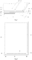
- Fig. 1 is a structure schematic view of a display device provided by an embodiment of the invention
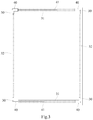
- Fig. 2 is an arrangement schematic view of a shading tape and a display panel of a display device provided by an embodiment of the invention
- Fig. 3 is an arrangement schematic view of a shading tape and a display panel of another display device provided by an embodiment of the invention
- Fig. 4 is an arrangement schematic view of a shading tape and a display panel of another display device provided by an embodiment of the invention
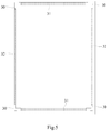
- Fig. 5 is an arrangement schematic view of a shading tape and a display panel of another display device provided by an embodiment of the invention.
- the display device comprises a display panel 1 and a backlight module 2, which backlight module 2 comprises a back plate 20, a light guide plate 21 and a light strip 22 mounted in the back plate 20, the display panel 1 having a polygon structure and being mounted on the back plate 20, and a shading tape 3 disposed along the edges of the display panel 1 being provided between the back plate 20 of the backlight module 2 and the display panel 1; in the edges of the display panel 1, an edge opposite to a side of the light strip 22 which faces the display panel 1 and having a extending direction parallel to that of the light strip 22 is a light incoming edge, that is, in the edges of the display panel 1, an edge close to the light strip 22 and having a extending direction parallel to that of the light strip 22 is the light incoming edge; each end of the light incoming edge forms a light incoming corner with an end of an adjacent edge, and the portion of the edge except the ends is a main body of the edge; the shading tape 30 provided at each light
- the shading tape 30 provided at each light incoming corner, the shading tape 31 provided at the main body of the light incoming edge, and the shading tape 32 provided at the main body of the adjacent edge forming the light incoming corner with the light incoming edge have a separated structure; and only the shading tape 30 provided at the parts of the edges of the display panel 1 except the light incoming corners is provided with an adhesive layer, that is, the side, which faces the display panel 1, of the shading tape 30 provided at the light incoming corners is not provided with an adhesive layer, so the parts of the display panel 1 which correspond to the light incoming corners would not be stuck by the shading tape 30, and thus would not create extrusive stress due to the sticking of the shading tape 30. Therefore, a phenomenon of water ripple and light leakage does not easily occur in a portion of a display panel 1 which corresponds to a light incoming corner.
- the backlight module 2 further comprises a prism 23 mounted in the back plate 20 and located between the light guide plate 21 and the display panel 1, a protection layer 24 located between the prism 23 and the display panel 1; the shading tape 3 is located between the display panel 1 and the protection layer 24 of the backlight module 2.
- a side, which faces the backlight module 2, of the shading tape 3 provided at the edges of the display panel 1 is provided with an adhesive layer, and a side of the shading tape 3 which faces the backlight module 2 is stuck to the protection layer 24 of the backlight module 2 and to the back plate 20, for shielding the light coming into the edge of the display panel 1.
- the display panel 1 comprises a lower polarizer 10, an array substrate 11, a color film layer 12 and a upper polarizer 13 which are arranged in turn from the light incoming side to the light outgoing side; when a side of the lower polarizer 10 which is near the light incoming edge is located on a side of the array substrate 11 which faces the backlight module 2, and a stepped structure is formed between the lower polarizer 10 and the array substrate 11, an adhesive strip 4 is provided between the shading tape 3 at the light incoming edge and at the light incoming corner and the array substrate 11, and the adhesive strip 4 is able to compensate for the gap in a panel thickness direction between the shading tape 3 and the array substrate 11.
- Fig. 4 is a structure diagram of the display panel with one light incoming edge and without the adhesive strip
- Fig. 5 is a structure diagram of the display panel with two light incoming edges and without the adhesive strip.
- the adhesive strip 40 provided between each the light incoming corner and the array substrate 11 and the adhesive strip 41 provided between the main body of the light incoming edge and the array substrate 11 have a separated structure; in the side, which faces the display panel, of the adhesive strip 40 provided between the light incoming corner and the array substrate 11 and the adhesive strip 41 provided between the main body of the light incoming edge and the array substrate 11, only the adhesive strip 41 provided between the main body of the light incoming edge and the array substrate 11 is provided with an adhesive layer, and the side of the adhesive strip 41 which faces the display panel 1 is stuck to the array substrate 11.
- the adhesive strip 40 provided between each the light incoming corner and the array substrate 11 and the adhesive strip 41 provided between the main body of the light incoming edge and the array substrate 11 have a separated structure, and the side, which faces the display panel 1, of the adhesive strip 40 provided between the light incoming corner and the array substrate 11 is not provided with an adhesive layer, the light incoming corner would not cause water ripple creating in the picture of the display panel 1 due to the extrusive stress generated by sticking adhesive strip 4. Therefore, a phenomenon of water ripple and light leakage does not occur in a portion, which corresponds to a light incoming corner, of the display panel 1, due to stick the adhesive strip 4.
- an adhesive layer is provided in the side, which faces the shading tape 3, of the adhesive strip 40 provided between each the light incoming corner and the array substrate 11 and the adhesive strip 41 provided between the main body of the light incoming edge and the array substrate 11, that is, the side of the adhesive strips 4 which faces the shading tape 3 is provided with an adhesive layer and is stuck to the shading tape 3.
- the backlight module 2 may comprise two light strips 22, which are disposed oppositely to two opposite sides of the light guide plate 21.
- the display panel has two light incoming edges and four light incoming corners.
- the shading tape 30 provided at each light incoming corner of the display panel 1, the shading tape 31 provided at the main bodies of the light incoming edges, and the shading tape 32 provided at the main bodies of the adjacent edges forming the light incoming corners with the light incoming edges have a separated structure, and the side, which faces the display panel 1, of the shading tape 30 provided at the light incoming corners is not provided with an adhesive layer, so the light incoming corners of the display panel 1 would not appear a phenomenon of water ripple and light leakage.
Landscapes
- Physics & Mathematics (AREA)
- Nonlinear Science (AREA)
- General Physics & Mathematics (AREA)
- Optics & Photonics (AREA)
- Mathematical Physics (AREA)
- Chemical & Material Sciences (AREA)
- Crystallography & Structural Chemistry (AREA)
- Liquid Crystal (AREA)
- Planar Illumination Modules (AREA)
Applications Claiming Priority (2)
| Application Number | Priority Date | Filing Date | Title |
|---|---|---|---|
| CN201510056050.6A CN104570485B (zh) | 2015-02-03 | 2015-02-03 | 一种显示装置 |
| PCT/CN2015/084353 WO2016123915A1 (zh) | 2015-02-03 | 2015-07-17 | 一种显示装置 |
Publications (3)
| Publication Number | Publication Date |
|---|---|
| EP3255486A1 true EP3255486A1 (de) | 2017-12-13 |
| EP3255486A4 EP3255486A4 (de) | 2018-09-05 |
| EP3255486B1 EP3255486B1 (de) | 2019-10-02 |
Family
ID=53086943
Family Applications (1)
| Application Number | Title | Priority Date | Filing Date |
|---|---|---|---|
| EP15837077.5A Active EP3255486B1 (de) | 2015-02-03 | 2015-07-17 | Anzeigevorrichtung |
Country Status (4)
| Country | Link |
|---|---|
| US (1) | US9971186B2 (de) |
| EP (1) | EP3255486B1 (de) |
| CN (1) | CN104570485B (de) |
| WO (1) | WO2016123915A1 (de) |
Cited By (1)
| Publication number | Priority date | Publication date | Assignee | Title |
|---|---|---|---|---|
| KR20210011551A (ko) * | 2019-07-22 | 2021-02-02 | 삼성디스플레이 주식회사 | 윈도우 부재, 이를 포함하는 전자 장치 및 윈도우 부재의 제조 방법 |
Families Citing this family (15)
| Publication number | Priority date | Publication date | Assignee | Title |
|---|---|---|---|---|
| CN104570485B (zh) * | 2015-02-03 | 2017-05-03 | 北京京东方茶谷电子有限公司 | 一种显示装置 |
| CN106200129B (zh) * | 2016-09-30 | 2019-11-05 | 京东方科技集团股份有限公司 | 背光模组及其制造方法、显示器模组及环形遮光胶带 |
| CN107340652B (zh) * | 2017-09-11 | 2020-05-15 | 京东方科技集团股份有限公司 | 封装胶、背光模组以及显示装置 |
| CN108286681B (zh) * | 2018-01-31 | 2021-01-15 | Oppo广东移动通信有限公司 | 电子装置及其显示组件、背光模组 |
| CN108302385B (zh) * | 2018-01-31 | 2021-01-15 | Oppo广东移动通信有限公司 | 一种背光模组及电子装置 |
| CN108302386B (zh) * | 2018-01-31 | 2021-01-15 | Oppo广东移动通信有限公司 | 电子装置及其显示组件、背光模组 |
| CN108150896B (zh) * | 2018-01-31 | 2021-01-15 | Oppo广东移动通信有限公司 | 电子装置及其背光模组 |
| CN108320666A (zh) * | 2018-02-08 | 2018-07-24 | 业成科技(成都)有限公司 | 显示装置 |
| CN109031781A (zh) * | 2018-07-27 | 2018-12-18 | 深圳市宝明科技股份有限公司 | 一种用于背光源的具有侧边包覆结构的遮光胶的制备方法 |
| CN109164635A (zh) * | 2018-09-20 | 2019-01-08 | 厦门天马微电子有限公司 | 背光模组及其制造方法及显示装置 |
| CN113037949B (zh) * | 2019-12-09 | 2022-07-26 | 宁波舜宇光电信息有限公司 | 滤光组件、摄像模组及多摄模组 |
| CN111290154A (zh) | 2020-02-24 | 2020-06-16 | 京东方科技集团股份有限公司 | 显示装置和拼接屏 |
| CN114002875B (zh) * | 2020-07-27 | 2023-10-27 | 海信视像科技股份有限公司 | 显示装置 |
| CN111983846A (zh) * | 2020-08-19 | 2020-11-24 | 武汉华星光电技术有限公司 | 显示装置 |
| CN113759617A (zh) * | 2021-09-22 | 2021-12-07 | 创维液晶器件(深圳)有限公司 | 液晶显示模组及制作方法、液晶显示装置 |
Family Cites Families (18)
| Publication number | Priority date | Publication date | Assignee | Title |
|---|---|---|---|---|
| JP2001108987A (ja) * | 1999-10-06 | 2001-04-20 | Nidec Copal Corp | 面発光装置 |
| JP2005084510A (ja) * | 2003-09-10 | 2005-03-31 | Seiko Epson Corp | 電気光学装置、および電気光学装置を備えた電子機器 |
| TWI327206B (en) * | 2007-07-16 | 2010-07-11 | Au Optronics Corp | Display device with shielding adhesive layer and method for manufacturing the same |
| US7800718B2 (en) | 2007-08-02 | 2010-09-21 | Seiko Epson Corporation | Electro-optical device and electronic apparatus having a light-shielding film at least partially overlapping with a transistor in plan view and having a plurality of openings overlapping with the transistor |
| JP5024793B2 (ja) * | 2007-10-19 | 2012-09-12 | Nltテクノロジー株式会社 | 表示装置 |
| JP4665983B2 (ja) * | 2008-03-28 | 2011-04-06 | ソニー株式会社 | 電気光学装置および電子機器 |
| JP5422051B2 (ja) | 2010-06-22 | 2014-02-19 | シャープ株式会社 | 表示パネルおよび表示装置 |
| CN102109689B (zh) * | 2010-12-30 | 2012-11-21 | 友达光电(苏州)有限公司 | 液晶显示器及此液晶显示器的液晶显示面板的拆解方法 |
| CN202056679U (zh) * | 2011-04-15 | 2011-11-30 | 郎应红 | 一种液晶显示背光源结构 |
| US9488772B2 (en) * | 2011-07-11 | 2016-11-08 | Seiko Epson Corporation | Display device, electronic apparatus and illumination device |
| CN102289089B (zh) * | 2011-07-22 | 2013-06-12 | 友达光电(厦门)有限公司 | 平面显示器 |
| US20130258232A1 (en) * | 2012-03-30 | 2013-10-03 | Shenzhen China Star Optoelectronics Technology Co. Ltd. | Middle Frame and Liquid Crystal Display Module |
| CN202870439U (zh) * | 2012-08-30 | 2013-04-10 | 无锡世成晶电柔性线路板有限公司 | 液晶显示器 |
| US20150253484A1 (en) * | 2012-10-18 | 2015-09-10 | Sharp Kabushiki Kaisha | Illumination device and display device |
| CN203561805U (zh) * | 2013-06-28 | 2014-04-23 | 上海天马微电子有限公司 | 液晶显示模组结构及液晶显示装置 |
| CN203757522U (zh) | 2014-03-31 | 2014-08-06 | 北京京东方茶谷电子有限公司 | 一种背光模组及显示装置 |
| CN204127794U (zh) | 2014-10-21 | 2015-01-28 | 厦门天马微电子有限公司 | 背光模组及液晶显示装置 |
| CN104570485B (zh) * | 2015-02-03 | 2017-05-03 | 北京京东方茶谷电子有限公司 | 一种显示装置 |
-
2015
- 2015-02-03 CN CN201510056050.6A patent/CN104570485B/zh active Active
- 2015-07-17 WO PCT/CN2015/084353 patent/WO2016123915A1/zh not_active Ceased
- 2015-07-17 US US14/893,913 patent/US9971186B2/en active Active
- 2015-07-17 EP EP15837077.5A patent/EP3255486B1/de active Active
Cited By (2)
| Publication number | Priority date | Publication date | Assignee | Title |
|---|---|---|---|---|
| KR20210011551A (ko) * | 2019-07-22 | 2021-02-02 | 삼성디스플레이 주식회사 | 윈도우 부재, 이를 포함하는 전자 장치 및 윈도우 부재의 제조 방법 |
| US12044866B2 (en) | 2019-07-22 | 2024-07-23 | Samsung Display Co., Ltd. | Window member, electronic apparatus including the same, and manufacturing method of window member |
Also Published As
| Publication number | Publication date |
|---|---|
| EP3255486B1 (de) | 2019-10-02 |
| EP3255486A4 (de) | 2018-09-05 |
| CN104570485B (zh) | 2017-05-03 |
| CN104570485A (zh) | 2015-04-29 |
| US9971186B2 (en) | 2018-05-15 |
| US20160357060A1 (en) | 2016-12-08 |
| WO2016123915A1 (zh) | 2016-08-11 |
Similar Documents
| Publication | Publication Date | Title |
|---|---|---|
| EP3255486B1 (de) | Anzeigevorrichtung | |
| US9897739B2 (en) | Optical film, backlight module, and display device | |
| US9594208B2 (en) | Backlight module and display device | |
| KR102301094B1 (ko) | 표시 장치 | |
| JP6440227B2 (ja) | バックライトモジュール及び表示装置 | |
| JP2019045855A (ja) | フレキシブルディスプレイ装置 | |
| US9817265B2 (en) | Display panel and display device | |
| US10012791B2 (en) | Rubber frame, backlight module and display device | |
| WO2019047151A1 (zh) | 一种显示模组、显示面板、显示装置及电子设备 | |
| KR20170015803A (ko) | 플렉서블 표시패널을 이용한 멀티비젼 표시장치 | |
| US11914239B2 (en) | Multi-screen and display device | |
| WO2016176929A1 (zh) | 背光模块及液晶显示器 | |
| US20160091743A1 (en) | Curved liquid crystal display | |
| WO2016173024A1 (zh) | 背光模组及显示器 | |
| US20170108640A1 (en) | Backlight module and display device | |
| CN108089365A (zh) | 显示装置 | |
| KR102293647B1 (ko) | 디스플레이 장치 | |
| CN205301764U (zh) | 一种背光源模组及显示装置 | |
| KR102173639B1 (ko) | 디스플레이 장치 | |
| CN104932042B (zh) | 背光模块及其光学膜片的保护膜 | |
| US20170020008A1 (en) | Display System Having Borderless Design | |
| KR20160015476A (ko) | 표시 장치 | |
| CN104534348B (zh) | 一种背光模组及显示装置 | |
| US20170219873A1 (en) | Liquid crystal panel and liquid crystal display device | |
| US9696586B2 (en) | Backlight module and a display device |
Legal Events
| Date | Code | Title | Description |
|---|---|---|---|
| STAA | Information on the status of an ep patent application or granted ep patent |
Free format text: STATUS: THE INTERNATIONAL PUBLICATION HAS BEEN MADE |
|
| PUAI | Public reference made under article 153(3) epc to a published international application that has entered the european phase |
Free format text: ORIGINAL CODE: 0009012 |
|
| STAA | Information on the status of an ep patent application or granted ep patent |
Free format text: STATUS: REQUEST FOR EXAMINATION WAS MADE |
|
| 17P | Request for examination filed |
Effective date: 20160304 |
|
| AK | Designated contracting states |
Kind code of ref document: A1 Designated state(s): AL AT BE BG CH CY CZ DE DK EE ES FI FR GB GR HR HU IE IS IT LI LT LU LV MC MK MT NL NO PL PT RO RS SE SI SK SM TR |
|
| AX | Request for extension of the european patent |
Extension state: BA ME |
|
| DAV | Request for validation of the european patent (deleted) | ||
| DAX | Request for extension of the european patent (deleted) | ||
| A4 | Supplementary search report drawn up and despatched |
Effective date: 20180802 |
|
| RIC1 | Information provided on ipc code assigned before grant |
Ipc: G02F 1/13357 20060101AFI20180727BHEP |
|
| GRAP | Despatch of communication of intention to grant a patent |
Free format text: ORIGINAL CODE: EPIDOSNIGR1 |
|
| STAA | Information on the status of an ep patent application or granted ep patent |
Free format text: STATUS: GRANT OF PATENT IS INTENDED |
|
| INTG | Intention to grant announced |
Effective date: 20190506 |
|
| GRAS | Grant fee paid |
Free format text: ORIGINAL CODE: EPIDOSNIGR3 |
|
| GRAA | (expected) grant |
Free format text: ORIGINAL CODE: 0009210 |
|
| STAA | Information on the status of an ep patent application or granted ep patent |
Free format text: STATUS: THE PATENT HAS BEEN GRANTED |
|
| AK | Designated contracting states |
Kind code of ref document: B1 Designated state(s): AL AT BE BG CH CY CZ DE DK EE ES FI FR GB GR HR HU IE IS IT LI LT LU LV MC MK MT NL NO PL PT RO RS SE SI SK SM TR |
|
| REG | Reference to a national code |
Ref country code: GB Ref legal event code: FG4D |
|
| REG | Reference to a national code |
Ref country code: CH Ref legal event code: EP Ref country code: AT Ref legal event code: REF Ref document number: 1186853 Country of ref document: AT Kind code of ref document: T Effective date: 20191015 |
|
| REG | Reference to a national code |
Ref country code: IE Ref legal event code: FG4D |
|
| REG | Reference to a national code |
Ref country code: DE Ref legal event code: R096 Ref document number: 602015039236 Country of ref document: DE |
|
| REG | Reference to a national code |
Ref country code: NL Ref legal event code: MP Effective date: 20191002 |
|
| REG | Reference to a national code |
Ref country code: LT Ref legal event code: MG4D |
|
| REG | Reference to a national code |
Ref country code: AT Ref legal event code: MK05 Ref document number: 1186853 Country of ref document: AT Kind code of ref document: T Effective date: 20191002 |
|
| PG25 | Lapsed in a contracting state [announced via postgrant information from national office to epo] |
Ref country code: SE Free format text: LAPSE BECAUSE OF FAILURE TO SUBMIT A TRANSLATION OF THE DESCRIPTION OR TO PAY THE FEE WITHIN THE PRESCRIBED TIME-LIMIT Effective date: 20191002 Ref country code: AT Free format text: LAPSE BECAUSE OF FAILURE TO SUBMIT A TRANSLATION OF THE DESCRIPTION OR TO PAY THE FEE WITHIN THE PRESCRIBED TIME-LIMIT Effective date: 20191002 Ref country code: LV Free format text: LAPSE BECAUSE OF FAILURE TO SUBMIT A TRANSLATION OF THE DESCRIPTION OR TO PAY THE FEE WITHIN THE PRESCRIBED TIME-LIMIT Effective date: 20191002 Ref country code: NL Free format text: LAPSE BECAUSE OF FAILURE TO SUBMIT A TRANSLATION OF THE DESCRIPTION OR TO PAY THE FEE WITHIN THE PRESCRIBED TIME-LIMIT Effective date: 20191002 Ref country code: NO Free format text: LAPSE BECAUSE OF FAILURE TO SUBMIT A TRANSLATION OF THE DESCRIPTION OR TO PAY THE FEE WITHIN THE PRESCRIBED TIME-LIMIT Effective date: 20200102 Ref country code: GR Free format text: LAPSE BECAUSE OF FAILURE TO SUBMIT A TRANSLATION OF THE DESCRIPTION OR TO PAY THE FEE WITHIN THE PRESCRIBED TIME-LIMIT Effective date: 20200103 Ref country code: LT Free format text: LAPSE BECAUSE OF FAILURE TO SUBMIT A TRANSLATION OF THE DESCRIPTION OR TO PAY THE FEE WITHIN THE PRESCRIBED TIME-LIMIT Effective date: 20191002 Ref country code: ES Free format text: LAPSE BECAUSE OF FAILURE TO SUBMIT A TRANSLATION OF THE DESCRIPTION OR TO PAY THE FEE WITHIN THE PRESCRIBED TIME-LIMIT Effective date: 20191002 Ref country code: PL Free format text: LAPSE BECAUSE OF FAILURE TO SUBMIT A TRANSLATION OF THE DESCRIPTION OR TO PAY THE FEE WITHIN THE PRESCRIBED TIME-LIMIT Effective date: 20191002 Ref country code: PT Free format text: LAPSE BECAUSE OF FAILURE TO SUBMIT A TRANSLATION OF THE DESCRIPTION OR TO PAY THE FEE WITHIN THE PRESCRIBED TIME-LIMIT Effective date: 20200203 Ref country code: FI Free format text: LAPSE BECAUSE OF FAILURE TO SUBMIT A TRANSLATION OF THE DESCRIPTION OR TO PAY THE FEE WITHIN THE PRESCRIBED TIME-LIMIT Effective date: 20191002 Ref country code: BG Free format text: LAPSE BECAUSE OF FAILURE TO SUBMIT A TRANSLATION OF THE DESCRIPTION OR TO PAY THE FEE WITHIN THE PRESCRIBED TIME-LIMIT Effective date: 20200102 |
|
| PG25 | Lapsed in a contracting state [announced via postgrant information from national office to epo] |
Ref country code: HR Free format text: LAPSE BECAUSE OF FAILURE TO SUBMIT A TRANSLATION OF THE DESCRIPTION OR TO PAY THE FEE WITHIN THE PRESCRIBED TIME-LIMIT Effective date: 20191002 Ref country code: RS Free format text: LAPSE BECAUSE OF FAILURE TO SUBMIT A TRANSLATION OF THE DESCRIPTION OR TO PAY THE FEE WITHIN THE PRESCRIBED TIME-LIMIT Effective date: 20191002 Ref country code: IS Free format text: LAPSE BECAUSE OF FAILURE TO SUBMIT A TRANSLATION OF THE DESCRIPTION OR TO PAY THE FEE WITHIN THE PRESCRIBED TIME-LIMIT Effective date: 20200224 Ref country code: CZ Free format text: LAPSE BECAUSE OF FAILURE TO SUBMIT A TRANSLATION OF THE DESCRIPTION OR TO PAY THE FEE WITHIN THE PRESCRIBED TIME-LIMIT Effective date: 20191002 |
|
| PG25 | Lapsed in a contracting state [announced via postgrant information from national office to epo] |
Ref country code: AL Free format text: LAPSE BECAUSE OF FAILURE TO SUBMIT A TRANSLATION OF THE DESCRIPTION OR TO PAY THE FEE WITHIN THE PRESCRIBED TIME-LIMIT Effective date: 20191002 |
|
| REG | Reference to a national code |
Ref country code: DE Ref legal event code: R097 Ref document number: 602015039236 Country of ref document: DE |
|
| PG2D | Information on lapse in contracting state deleted |
Ref country code: IS |
|
| PG25 | Lapsed in a contracting state [announced via postgrant information from national office to epo] |
Ref country code: RO Free format text: LAPSE BECAUSE OF FAILURE TO SUBMIT A TRANSLATION OF THE DESCRIPTION OR TO PAY THE FEE WITHIN THE PRESCRIBED TIME-LIMIT Effective date: 20191002 Ref country code: DK Free format text: LAPSE BECAUSE OF FAILURE TO SUBMIT A TRANSLATION OF THE DESCRIPTION OR TO PAY THE FEE WITHIN THE PRESCRIBED TIME-LIMIT Effective date: 20191002 Ref country code: EE Free format text: LAPSE BECAUSE OF FAILURE TO SUBMIT A TRANSLATION OF THE DESCRIPTION OR TO PAY THE FEE WITHIN THE PRESCRIBED TIME-LIMIT Effective date: 20191002 Ref country code: IS Free format text: LAPSE BECAUSE OF FAILURE TO SUBMIT A TRANSLATION OF THE DESCRIPTION OR TO PAY THE FEE WITHIN THE PRESCRIBED TIME-LIMIT Effective date: 20200202 |
|
| PLBE | No opposition filed within time limit |
Free format text: ORIGINAL CODE: 0009261 |
|
| STAA | Information on the status of an ep patent application or granted ep patent |
Free format text: STATUS: NO OPPOSITION FILED WITHIN TIME LIMIT |
|
| PG25 | Lapsed in a contracting state [announced via postgrant information from national office to epo] |
Ref country code: SK Free format text: LAPSE BECAUSE OF FAILURE TO SUBMIT A TRANSLATION OF THE DESCRIPTION OR TO PAY THE FEE WITHIN THE PRESCRIBED TIME-LIMIT Effective date: 20191002 Ref country code: IT Free format text: LAPSE BECAUSE OF FAILURE TO SUBMIT A TRANSLATION OF THE DESCRIPTION OR TO PAY THE FEE WITHIN THE PRESCRIBED TIME-LIMIT Effective date: 20191002 Ref country code: SM Free format text: LAPSE BECAUSE OF FAILURE TO SUBMIT A TRANSLATION OF THE DESCRIPTION OR TO PAY THE FEE WITHIN THE PRESCRIBED TIME-LIMIT Effective date: 20191002 |
|
| 26N | No opposition filed |
Effective date: 20200703 |
|
| PG25 | Lapsed in a contracting state [announced via postgrant information from national office to epo] |
Ref country code: SI Free format text: LAPSE BECAUSE OF FAILURE TO SUBMIT A TRANSLATION OF THE DESCRIPTION OR TO PAY THE FEE WITHIN THE PRESCRIBED TIME-LIMIT Effective date: 20191002 |
|
| PG25 | Lapsed in a contracting state [announced via postgrant information from national office to epo] |
Ref country code: MC Free format text: LAPSE BECAUSE OF FAILURE TO SUBMIT A TRANSLATION OF THE DESCRIPTION OR TO PAY THE FEE WITHIN THE PRESCRIBED TIME-LIMIT Effective date: 20191002 |
|
| REG | Reference to a national code |
Ref country code: CH Ref legal event code: PL |
|
| GBPC | Gb: european patent ceased through non-payment of renewal fee |
Effective date: 20200717 |
|
| REG | Reference to a national code |
Ref country code: BE Ref legal event code: MM Effective date: 20200731 |
|
| PG25 | Lapsed in a contracting state [announced via postgrant information from national office to epo] |
Ref country code: CH Free format text: LAPSE BECAUSE OF NON-PAYMENT OF DUE FEES Effective date: 20200731 Ref country code: GB Free format text: LAPSE BECAUSE OF NON-PAYMENT OF DUE FEES Effective date: 20200717 Ref country code: LU Free format text: LAPSE BECAUSE OF NON-PAYMENT OF DUE FEES Effective date: 20200717 Ref country code: LI Free format text: LAPSE BECAUSE OF NON-PAYMENT OF DUE FEES Effective date: 20200731 Ref country code: FR Free format text: LAPSE BECAUSE OF NON-PAYMENT OF DUE FEES Effective date: 20200731 |
|
| PG25 | Lapsed in a contracting state [announced via postgrant information from national office to epo] |
Ref country code: BE Free format text: LAPSE BECAUSE OF NON-PAYMENT OF DUE FEES Effective date: 20200731 |
|
| PG25 | Lapsed in a contracting state [announced via postgrant information from national office to epo] |
Ref country code: IE Free format text: LAPSE BECAUSE OF NON-PAYMENT OF DUE FEES Effective date: 20200717 |
|
| PG25 | Lapsed in a contracting state [announced via postgrant information from national office to epo] |
Ref country code: TR Free format text: LAPSE BECAUSE OF FAILURE TO SUBMIT A TRANSLATION OF THE DESCRIPTION OR TO PAY THE FEE WITHIN THE PRESCRIBED TIME-LIMIT Effective date: 20191002 Ref country code: MT Free format text: LAPSE BECAUSE OF FAILURE TO SUBMIT A TRANSLATION OF THE DESCRIPTION OR TO PAY THE FEE WITHIN THE PRESCRIBED TIME-LIMIT Effective date: 20191002 Ref country code: CY Free format text: LAPSE BECAUSE OF FAILURE TO SUBMIT A TRANSLATION OF THE DESCRIPTION OR TO PAY THE FEE WITHIN THE PRESCRIBED TIME-LIMIT Effective date: 20191002 |
|
| PG25 | Lapsed in a contracting state [announced via postgrant information from national office to epo] |
Ref country code: MK Free format text: LAPSE BECAUSE OF FAILURE TO SUBMIT A TRANSLATION OF THE DESCRIPTION OR TO PAY THE FEE WITHIN THE PRESCRIBED TIME-LIMIT Effective date: 20191002 |
|
| PGFP | Annual fee paid to national office [announced via postgrant information from national office to epo] |
Ref country code: DE Payment date: 20250728 Year of fee payment: 11 |