EP3248218B1 - Verbundgehäuse mit sandwichstruktur für eine vorrichtung - Google Patents
Verbundgehäuse mit sandwichstruktur für eine vorrichtung Download PDFInfo
- Publication number
- EP3248218B1 EP3248218B1 EP16705347.9A EP16705347A EP3248218B1 EP 3248218 B1 EP3248218 B1 EP 3248218B1 EP 16705347 A EP16705347 A EP 16705347A EP 3248218 B1 EP3248218 B1 EP 3248218B1
- Authority
- EP
- European Patent Office
- Prior art keywords
- conductive layer
- layer
- electronic components
- structured composite
- composite housing
- Prior art date
- Legal status (The legal status is an assumption and is not a legal conclusion. Google has not performed a legal analysis and makes no representation as to the accuracy of the status listed.)
- Active
Links
Images



Classifications
-
- G—PHYSICS
- G06—COMPUTING OR CALCULATING; COUNTING
- G06F—ELECTRIC DIGITAL DATA PROCESSING
- G06F1/00—Details not covered by groups G06F3/00 - G06F13/00 and G06F21/00
- G06F1/16—Constructional details or arrangements
- G06F1/20—Cooling means
- G06F1/203—Cooling means for portable computers, e.g. for laptops
-
- G—PHYSICS
- G06—COMPUTING OR CALCULATING; COUNTING
- G06F—ELECTRIC DIGITAL DATA PROCESSING
- G06F1/00—Details not covered by groups G06F3/00 - G06F13/00 and G06F21/00
- G06F1/16—Constructional details or arrangements
- G06F1/1613—Constructional details or arrangements for portable computers
- G06F1/1626—Constructional details or arrangements for portable computers with a single-body enclosure integrating a flat display, e.g. Personal Digital Assistants [PDAs]
-
- G—PHYSICS
- G06—COMPUTING OR CALCULATING; COUNTING
- G06F—ELECTRIC DIGITAL DATA PROCESSING
- G06F1/00—Details not covered by groups G06F3/00 - G06F13/00 and G06F21/00
- G06F1/16—Constructional details or arrangements
- G06F1/1613—Constructional details or arrangements for portable computers
- G06F1/1633—Constructional details or arrangements of portable computers not specific to the type of enclosures covered by groups G06F1/1615 - G06F1/1626
- G06F1/1637—Details related to the display arrangement, including those related to the mounting of the display in the housing
- G06F1/1643—Details related to the display arrangement, including those related to the mounting of the display in the housing the display being associated to a digitizer, e.g. laptops that can be used as penpads
-
- G—PHYSICS
- G06—COMPUTING OR CALCULATING; COUNTING
- G06F—ELECTRIC DIGITAL DATA PROCESSING
- G06F1/00—Details not covered by groups G06F3/00 - G06F13/00 and G06F21/00
- G06F1/16—Constructional details or arrangements
- G06F1/1613—Constructional details or arrangements for portable computers
- G06F1/1633—Constructional details or arrangements of portable computers not specific to the type of enclosures covered by groups G06F1/1615 - G06F1/1626
- G06F1/1656—Details related to functional adaptations of the enclosure, e.g. to provide protection against EMI, shock, water, or to host detachable peripherals like a mouse or removable expansions units like PCMCIA cards, or to provide access to internal components for maintenance or to removable storage supports like CDs or DVDs, or to mechanically mount accessories
- G06F1/1658—Details related to functional adaptations of the enclosure, e.g. to provide protection against EMI, shock, water, or to host detachable peripherals like a mouse or removable expansions units like PCMCIA cards, or to provide access to internal components for maintenance or to removable storage supports like CDs or DVDs, or to mechanically mount accessories related to the mounting of internal components, e.g. disc drive or any other functional module
-
- G—PHYSICS
- G06—COMPUTING OR CALCULATING; COUNTING
- G06F—ELECTRIC DIGITAL DATA PROCESSING
- G06F3/00—Input arrangements for transferring data to be processed into a form capable of being handled by the computer; Output arrangements for transferring data from processing unit to output unit, e.g. interface arrangements
- G06F3/01—Input arrangements or combined input and output arrangements for interaction between user and computer
- G06F3/03—Arrangements for converting the position or the displacement of a member into a coded form
- G06F3/041—Digitisers, e.g. for touch screens or touch pads, characterised by the transducing means
- G06F3/0412—Digitisers structurally integrated in a display
-
- G—PHYSICS
- G06—COMPUTING OR CALCULATING; COUNTING
- G06F—ELECTRIC DIGITAL DATA PROCESSING
- G06F3/00—Input arrangements for transferring data to be processed into a form capable of being handled by the computer; Output arrangements for transferring data from processing unit to output unit, e.g. interface arrangements
- G06F3/01—Input arrangements or combined input and output arrangements for interaction between user and computer
- G06F3/03—Arrangements for converting the position or the displacement of a member into a coded form
- G06F3/041—Digitisers, e.g. for touch screens or touch pads, characterised by the transducing means
- G06F3/045—Digitisers, e.g. for touch screens or touch pads, characterised by the transducing means using resistive elements, e.g. a single continuous surface or two parallel surfaces put in contact
-
- H—ELECTRICITY
- H05—ELECTRIC TECHNIQUES NOT OTHERWISE PROVIDED FOR
- H05K—PRINTED CIRCUITS; CASINGS OR CONSTRUCTIONAL DETAILS OF ELECTRIC APPARATUS; MANUFACTURE OF ASSEMBLAGES OF ELECTRICAL COMPONENTS
- H05K7/00—Constructional details common to different types of electric apparatus
- H05K7/20—Modifications to facilitate cooling, ventilating, or heating
- H05K7/2039—Modifications to facilitate cooling, ventilating, or heating characterised by the heat transfer by conduction from the heat generating element to a dissipating body
-
- H—ELECTRICITY
- H05—ELECTRIC TECHNIQUES NOT OTHERWISE PROVIDED FOR
- H05K—PRINTED CIRCUITS; CASINGS OR CONSTRUCTIONAL DETAILS OF ELECTRIC APPARATUS; MANUFACTURE OF ASSEMBLAGES OF ELECTRICAL COMPONENTS
- H05K7/00—Constructional details common to different types of electric apparatus
- H05K7/20—Modifications to facilitate cooling, ventilating, or heating
- H05K7/2039—Modifications to facilitate cooling, ventilating, or heating characterised by the heat transfer by conduction from the heat generating element to a dissipating body
- H05K7/20436—Inner thermal coupling elements in heat dissipating housings, e.g. protrusions or depressions integrally formed in the housing
-
- H—ELECTRICITY
- H10—SEMICONDUCTOR DEVICES; ELECTRIC SOLID-STATE DEVICES NOT OTHERWISE PROVIDED FOR
- H10W—GENERIC PACKAGES, INTERCONNECTIONS, CONNECTORS OR OTHER CONSTRUCTIONAL DETAILS OF DEVICES COVERED BY CLASS H10
- H10W40/00—Arrangements for thermal protection or thermal control
- H10W40/20—Arrangements for cooling
- H10W40/22—Arrangements for cooling characterised by their shape, e.g. having conical or cylindrical projections
-
- H—ELECTRICITY
- H10—SEMICONDUCTOR DEVICES; ELECTRIC SOLID-STATE DEVICES NOT OTHERWISE PROVIDED FOR
- H10W—GENERIC PACKAGES, INTERCONNECTIONS, CONNECTORS OR OTHER CONSTRUCTIONAL DETAILS OF DEVICES COVERED BY CLASS H10
- H10W40/00—Arrangements for thermal protection or thermal control
- H10W40/20—Arrangements for cooling
- H10W40/25—Arrangements for cooling characterised by their materials
- H10W40/255—Arrangements for cooling characterised by their materials having a laminate or multilayered structure, e.g. direct bond copper [DBC] ceramic substrates
-
- H—ELECTRICITY
- H10—SEMICONDUCTOR DEVICES; ELECTRIC SOLID-STATE DEVICES NOT OTHERWISE PROVIDED FOR
- H10W—GENERIC PACKAGES, INTERCONNECTIONS, CONNECTORS OR OTHER CONSTRUCTIONAL DETAILS OF DEVICES COVERED BY CLASS H10
- H10W40/00—Arrangements for thermal protection or thermal control
- H10W40/60—Securing means for detachable heating or cooling arrangements, e.g. clamps
- H10W40/611—Bolts or screws
-
- G—PHYSICS
- G06—COMPUTING OR CALCULATING; COUNTING
- G06F—ELECTRIC DIGITAL DATA PROCESSING
- G06F3/00—Input arrangements for transferring data to be processed into a form capable of being handled by the computer; Output arrangements for transferring data from processing unit to output unit, e.g. interface arrangements
- G06F3/01—Input arrangements or combined input and output arrangements for interaction between user and computer
- G06F3/03—Arrangements for converting the position or the displacement of a member into a coded form
- G06F3/041—Digitisers, e.g. for touch screens or touch pads, characterised by the transducing means
-
- H—ELECTRICITY
- H10—SEMICONDUCTOR DEVICES; ELECTRIC SOLID-STATE DEVICES NOT OTHERWISE PROVIDED FOR
- H10W—GENERIC PACKAGES, INTERCONNECTIONS, CONNECTORS OR OTHER CONSTRUCTIONAL DETAILS OF DEVICES COVERED BY CLASS H10
- H10W40/00—Arrangements for thermal protection or thermal control
- H10W40/20—Arrangements for cooling
- H10W40/231—Arrangements for cooling characterised by their places of attachment or cooling paths
- H10W40/242—Arrangements for cooling characterised by their places of attachment or cooling paths comprising thermal conductors between chips and the and the arrangements for cooling, e.g. compliant heat-spreaders
Definitions
- the description relates to devices, such as computing devices, and to housings for devices.
- the present concepts relate to devices, such as computing devices.
- devices such as computing devices.
- form factors such as tablets, notebooks, and/or wearable devices
- consumer preferences are toward smaller form factors, especially thinner and/or lighter form factors.
- consumers want high compute performance.
- the high performance tends to result in unwanted heat generation.
- Removing heat from the source within devices becomes increasingly difficult with thinner devices.
- venting has been removed for aesthetic reasons, as well as the difficulty involved with getting airflow through a thin device tightly packed with components.
- Current technology utilizes conductive materials such as aluminum, copper, and pyrolytic graphite to remove heat from the source and move it to another area. Structures are laminated with these conductive materials with the idea of removing heat from one area and distributing it evenly over a broader area.
- document US 2008/0151503 A1 proposes to solve the problem of "hot spots” by using an anisotropic heat spreading member, which quickly transfers the heat parallel to the planar region of the housing.
- the concepts underlying the present invention provide higher heat transfer efficiency and/or the ability to move heat from one surface to another within a device.
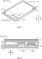
- FIGS. 1-2 show an example device 100 implemented as a tablet type computing device.
- FIG. 1 shows a partial cut-away view of device 100.
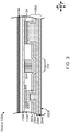
- FIG. 2 is a sectional view through device 100 as indicated in FIG. 1 .
- the device 100 can include first and second portions 102 and 104.
- the first portion is realised as a sandwich structured composite housing 106 and the second portion is realised as a display screen, such as a touch display 108.
- Computing device 100 can also include a set of heat generating electronic components 110.
- the set of electronic components can include processor 112 and memory 114.
- the processor 112 and memory 114 are secured to a printed circuit board 116 that can include other electronic components.
- the set of electronic components 110 can be positioned within the sandwich structured composite housing 106 with the touch display 108 positioned on top. Accordingly, in such instances the sandwich structured composite housing 106 is sometimes referred to as a 'bucket.'
- sandwich structured composite housing 106 includes inner and outer structural layers 202 and 204 as well as interposed thermal conductive and thermal insulative layers 206 and 208, respectively.
- the inner structural layer 202 defines windows 210 proximate to (e.g., beneath or along the z reference axis) individual heat generating electronic components.
- window 210(1) is located beneath processor 112 and window 210(2) is located beneath memory 114.
- the windows 210 allows the thermal conductive layer 206 to be extended toward (e.g., closer to) the heat generating electronic components 110 (e.g., in the positive z reference direction).
- the processor extends quite far toward the sandwich structured composite housing 106 in the z reference direction.
- the thermal conductive layer 206 is extended beyond the inner structural layer 202 (e.g., 'proud' to the inner structural layer) to be in close proximity to the memory for efficient heat transfer. Stated another way, extending the thermal conductive layer 206 toward the heat generating components can increase an amount of heat energy per unit time that can be transferred from the electronic components 110 by the thermal conductive layer 206. Further, the thermal conductive layer 206 can be configured to dissipate this captured heat energy laterally over a large portion of the device 100.
- the thermal conductive layer 206 is configured to efficiently move heat away from the heat generating components in the x and y reference directions rather than simply transferring the heat to the directly underlying portion of the outer structural layer 204.
- the thermal conductive layer can be anisotropic or it is more efficient at conveying thermal energy parallel to a planar region (e.g., parallel to the xy reference plane than perpendicular to the planar region (e.g., the z reference direction)).
- the structure of the sandwich structured composite housing 106 contributes to efficient heat removal from the heat generating electronic components 110 so that these components do not fail prematurely.
- the removed heat is efficiently distributed laterally (e.g., in the x and y reference directions) by the thermal conductive layer 206.
- the distributed heat is finally conducted from the thermal conductive layer 206 through the thermal insulative layer 208 to the outer structural layer 204 so that the outer structural layer is more evenly 'warm' rather than having hot spots directly under the heat generating electronic components.
- the sandwich structured composite housing 106 can be thought of as having a generally planar region in the xy reference plane that approximately corresponds to and underlies the touch display 108.
- the term 'generally' is used since (as is evident in FIG. 2 ) portions of the thermal conductive layer 206 extend through the plane when the plane is defined by the inner structural layer 202. While some implementations may be generally planar, the concepts are equally applicable to nonplanar implementations, such as curved smart phones, curved TVs, curved wearables, etc.
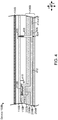
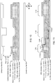
- FIG. 3 shows another device 100A that includes first and second portions 102A and 104A.
- the first portion 102A is realised as sandwich structured composite housing 106A.
- the set of electronic components 110A can include a general processor (e.g., CPU) 112A, a graphics processor (e.g., GPU) 302, and wireless circuitry 304, each of which is coupled to printed circuit board 116A.
- the graphics processor 302 has a curved surface 306 facing toward the sandwich structured composite housing 106A.
- a corresponding upper facing surface 308 of the thermal conductive layer 206A is shaped in an opposite manner (e.g., corresponding negative shape) to allow effective heat transfer from the graphics processor 302 to the thermal conductive layer 206A.
- the wireless circuitry 304 does not generate large amounts of heat, but structurally extends relatively far in the - z reference direction such that it would contact the inner structural layer 202A.
- the thermal conductive layer 206A is omitted below the wireless circuitry 304 as indicated at 310 and the inner structural layer 202 extends down into the space that would otherwise be occupied by the thermal conductive layer 206A.
- This configuration can create sufficient clearance between individual electronic components and the sandwich structured composite housing 106A.
- the bulk (e.g., z direction dimensions) of the wireless circuitry 304 would normally cause a thickness of the device to have to be increased, but the present implementations allow adaption of the bucket to accommodate the z direction dimensions of the wireless circuitry 304.
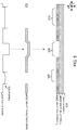
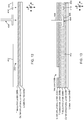
- FIG. 4 shows another device 100B.
- the thermal conductive layer 206B is shaped to be positioned against multiple surfaces 402 (e.g., a generally horizontal surface 402(1) and a generally vertical surface 402(2)) of processor 112B.
- a structural component 404 is embedded in the sandwich structured composite housing 106B.
- the structural component 404 includes a horizontally expanded base portion 406 (e.g. extends in the xy reference plane) located in the thermal insulative layer 208B and a vertical stem region 408 extending through the inner structural layer 202B toward the printed circuit board 116B.
- the structural component 404 can facilitate fastening the sandwich structured composite housing 106B to printed circuit board 116B or other elements.
- the structural component 404 is threaded to receive a fastener 410 through the printed circuit board 116B.
- a fastener 410 can be employed and/or the structural component 404 can be utilized in other ways and/or have other configurations.
- Device 100B also includes electronic components within the thermal insulative layer 208B or otherwise within the sandwich structured composite housing 106B.
- an individual electronic component 412 is implemented as an electrical conductor, such as a trace, that can electrically connect the printed circuit board to another element (not specifically shown).
- this electronic component 412 could function as an antenna.
- Another individual electronic component is implemented as a sensor 414 positioned within the sandwich structured composite housing 106B, in this this case within the thermal insulative layer 208B and against the outer structural layer 204B.
- the sensor 414 could be configured to sense conditions, such as pressure, through the outer structural layer 204B.
- the sensor 414 can be electrically connected to the printed circuit board via a trace 416, through various mechanisms, such as at the side of the structured composite housing 106B.
- the sandwich structured composite housing 106B can provide a very secure environment for these electronic components 412-416 so that they are secure from physical damage, water, corrosion, etc.
- the printed circuit board 116B can be readily grounded to portions of the thermal conductive layer 206B that are proud of (e.g., extend beyond) the inner structural layer 202B as indicated at 418.
- FIGS. 5-10 illustrate example processes for forming device 100A of FIG. 3 .
- FIG. 11 shows a similar device.
- FIGS. 12-15 illustrate example processes for forming device 100B of FIG. 4 . Further, FIGS. 5-15 include additional discussion about some of the elements of these devices.
- the assembly process can be accomplished with the aid of upper and lower platens or molds 502 and 504.
- the lower platen 504 is generally planar (e.g., has a linear profile) and the upper platen 502 approximates a portion of a profile 505 of the set of electronic components 110A (see Fig. 3 and compare to FIG. 5 ).
- FIG. 6 shows a view of thermal conductive layer 206A along the xy reference plane.
- the thermal conductive layer 206A is shaped so that no material of the layer occurs at area 508. Further, areas 506 and 510 occur proximate to heat generating electronic components.
- the thermal conductive layer 206A can efficiently diffuse heat from these areas to a large area 602 of the layer so that heat is spread throughout a majority of a surface of the device rather than being concentrated near the heat generating electronic components.
- FIG. 7 shows an alternative implementation of the thermal conductive layer manifest as an anisotropic thermal conductive layer 206A1.
- the anisotropic thermal conductive layer can be realised as a sheet of material.
- material usage can be reduced by shaping the sheet so that portions of the sheet are positioned proximate to the heat generating components (e.g., areas 506 and 510). Additional sheet material 702 and 704 can connect these areas 506 and 510 to a central area 706 that aids in even and widespread heat distribution.
- the stippled areas of the thermal conductive layer can be utilized as heat gathering areas which transfer heat to the non-stippled heat dissipation areas.
- Another portion 710 of the pyrolytic sheet can then be flipped or twisted at 712 so that the first surface is facing away from the heat generating component (e.g., toward the outside of the device and in this case toward the reader). Heat that is conducted laterally along the pyrolytic sheet from the surface facing away from the reader at portion 708 can travel along this 'flipped surface' so that it is more readily dissipated to the outside of the device at portion 710 (e.g., to the outer structural layer).
- the heat sources could be centrally located (e.g., positioned under the central area 706 (on the opposite side as the reader)). Heat could be conducted from the heat sources to the central area 706 and then dissipated throughout the surface of the device via the outer portions such as 506, 510, and 708. Further, twisting at 712 can be used so that heat that was captured on the surface of the graphite that was facing away from the reader and toward the heat source is now facing toward the reader and the outer structural layer 204A (see FIG. 5 ).
- some of the present implementations can take advantage of pyrolytic graphite's (or similar material's) ability to transfer heat in the X-Y plane readily, but not in the Z plane. This can allow for selective delivery of the heat to different surfaces by folding the pyrolytic graphite over within the structure. Selectively cutting and folding can allow a smaller piece of pyrolytic graphite to be utilized to reduce cost.
- an "origami" structure may be formed allowing heat to be moved radially around the center, and transferred from the inner surface to the outer surface farther away from the heat source.
- the pyrolytic graphite can be folded over to expose the hot side to the outer surface of the bucket in a location away from the heat source.
- Some implementations can employ the so-called "origami" structure where multiple strands and folds of the graphite could allow heat to travel along the inside of the device until a better location to couple to the outside of the device has been reached. At that point, the heated layer is now brought into contact with the outer layer to radiate heat externally to the device.
- the graphite has 10 equal legs cut into the sides, 5 legs on each side (though not illustrated, other geometric configurations are contemplated).
- the legs can be folded over to expose the side of the pyrolytic graphite that is transmitting heat well in the x-y plane.
- the heat source When this graphite is positioned between the heat source and the rear skin (e.g. outer structural layer) of the device, the heat source would be connected to the pyrolytic graphite, and the heat would be coupled away from the heat source to the outer skin. This would eliminate the hot spot that a customer might otherwise perceive at a specific area of the outer skin by distributing this heat evenly.
- FIG. 8 continues from FIG. 5 .
- the inner structural layer 202A is positioned over (e.g., against) the thermal conductive layer 206A and the upper platen 502 is positioned over (e.g., against) inner structural layer 202A.
- conditions can be created to cause thermal insulative layer 208A to expand.
- the temperature can be increased for a period of time to cause the thermal insulation to expand and cure into a relatively rigid bonding state.
- the conditions can be dictated by the specific thermal insulative layer composition utilized.
- the thermal insulative layer manufacturer can provide guidance to the conditions for their product.
- FIG. 9 shows the results after the expansion of the thermal insulative layer 208A forces the thermal conductive layer 206A up against the upper platen 502 to form the sandwich structured composite housing 106A.
- the thermal insulative layer has expanded and is now cured so that it provides bonding properties to secure the outer structural layer 204A, the thermal conductive layer 206A, and the inner structural layer 202A together as a 'sandwich structured composite' that has a collective strength greater than any of the individual elements.
- the thermal insulative layer can be selected from materials that when exposed to certain conditions, such as heat, the materials tend to expand. These conditions and/or other conditions can cause the material to cure to a state where the material functions as an adhesive. For instance, heating may cause the material to expand and then cooling the material may cause the material to cure and adhere to the surrounding materials.
- FIG. 11 shows an alternative version of a similar sandwich structured composite housing 106C.
- the thermal conductive layer 206C in areas 1102 and 1104 proximate to heat generating components (See 302 and 112A of FIG. 3 ) the thermal conductive layer 206C is positioned above the thermal insulative layer 208C (e.g., the thermal insulative layer 208C is closer to the outer structural layer 204C than is the thermal conductive layer 206C).
- the thermal conductive layer 206C is below thermal insulative layer 208C (e.g., closer to the outer structural layer 204C).
- This configuration can allow the thermal conductive layer 206C to be proximate to the heat generating components to pick up heat and then be proximate to the outer structural layer 204C to dissipate the heat.
- This configuration also lends itself to the 'flipped' thermal conductive layer configuration described above relative to FIG. 7 .
- the thermal conductive layer could be flipped 180 degrees in an intervening area 1108.
- heat can be picked up on an upward facing surface 1112(1) of the thermal conductive layer 206C proximate to the heat generating component. The heat can travel laterally along the thermal conductive layer.
- the upper facing surface 1112(2) becomes a downward facing surface that positions the captured heat against the outer structural layer 204A to be readily dissipated.
- FIG. 13 shows additional thermal insulative layer 208B positioned over the existing thin layer.
- the thermal conductive layer 206B can be positioned over the thermal insulative layer 208B.
- the inner structural layer 202B can be positioned over the thermal conductive layer 206B. Note that window 210B is formed in inner structural layer 202B directly under the location of processor 112B (see FIG. 4 ).
- One example is realised as a device that includes a metal composite material housing comprising inner and outer structural layers.
- the example can also include interposed thermal insulative and thermal conductive layers and components positioned over windows in the inner structural layer and the thermal conductive layer extending from between the inner and outer layers through the windows toward the components.
- the metal composite material housing defines a generally planar region, and wherein the heat generating electronic components are positioned over the generally planar region.
- a shape of an individual window corresponds to a shape of an individual heat generating electronic component positioned over the individual window when viewed through the generally planar region.
- thermal conductive layer occurs on an entirety of the generally planar region, or wherein the thermal conductive layer is selectively arranged on the generally planar region.
- thermal conductive layer comprises a sheet.
- thermal conductive layer comprises graphite, graphene or a carbon nanostructure.
- any combination of the above and/or below examples further comprising a structural member embedded in the thermal insulative layer and extending through the inner structural layer.
- Another example is realised as a computing device that includes a sandwich structured composite housing and a set of electronic components positioned over the sandwich structured composite housing.
- the set of electronic components having a profile against the sandwich structured composite housing, and the sandwich structured composite housing having a corresponding negative profile.
- the sandwich structured composite housing comprises a metal composite material.
- any combination of the above and/or below examples further comprising a touch display and wherein the set of electronic components are positioned between the sandwich structured composite housing and the touch display.
- any combination of the above and/or below examples further comprising another housing and wherein the set of electronic components are positioned between the sandwich structured composite housing and the another housing.
- the sandwich structured composite housing comprises an outer structural layer, a thermal insulative layer, a thermal conductive layer, and an inner structural layer.
- thermal conductive layer comprises a continuous sheet.
- Another example is realised as a sandwich structured composite housing that includes an inner structural layer defining a window and an outer structural layer.
- the example also includes an anisotropic thermal conductive layer, a first area of the thermal conductive layer positioned between the inner structural layer and the outer structural layer and a second area of the thermal conductive layer extending through the window beyond the inner structural layer.
- the example further includes a thermal insulative layer bonding the inner structural layer, the anisotropic thermal conductive layer, and the outer structural layer.
- anisotropic thermal conductive layer is generally continuous or is origami shaped.
Landscapes
- Engineering & Computer Science (AREA)
- Theoretical Computer Science (AREA)
- General Engineering & Computer Science (AREA)
- Computer Hardware Design (AREA)
- Physics & Mathematics (AREA)
- General Physics & Mathematics (AREA)
- Human Computer Interaction (AREA)
- Thermal Sciences (AREA)
- Microelectronics & Electronic Packaging (AREA)
- Cooling Or The Like Of Electrical Apparatus (AREA)
- Cooling Or The Like Of Semiconductors Or Solid State Devices (AREA)
- Chemical & Material Sciences (AREA)
- Ceramic Engineering (AREA)
Claims (12)
- Eine Vorrichtung, umfassend:
ein sandwichstrukturiertes Verbundgehäuse mit inneren (202) und äußeren Strukturschichten (204) und dazwischen liegenden wärmeisolierenden (208) und wärmeleitenden Schichten (206), wobei die wärmeleitende Schicht (206) über der wärmeisolierenden Schicht (208) angeordnet ist, die wiederum über der äußeren Strukturschicht (204) angeordnet ist; wobei elektronische Komponenten (112, 114) über Fenstern (210) in der inneren Strukturschicht (202) angeordnet sind,
wobei das sandwichstrukturierte Verbundgehäuse einen im Allgemeinen planaren Bereich definiert, dadurch gekennzeichnet, dass
die wärmeleitende Schicht (206) effizienter ist, um Wärmeenergie parallel zum planaren Bereich zu übertragen, als senkrecht zum planaren Bereich, und dass sich die wärmeleitende Schicht (206) von zwischen den inneren (202) und äußeren Strukturschichten (204) durch die Fenster zu den elektronischen Komponenten erstreckt. - Die Vorrichtung nach Anspruch 1, wobei die elektronischen Komponenten (112, 114) über dem im Allgemeinen planaren Bereich angeordnet sind.
- Vorrichtung nach Anspruch 2, wobei eine Form eines einzelnen Fensters (210) einer Form einer einzelnen elektronischen Komponente (112, 114) entspricht, die über dem einzelnen Fenster (210) positioniert ist, wenn sie entlang der Richtung orthogonal zum allgemein ebenen Bereich betrachtet wird.
- Die Vorrichtung nach Anspruch 2, wobei die wärmeleitende Schicht (206) auf einer Gesamtheit des im Allgemeinen planaren Bereichs angeordnet ist, oder wobei die wärmeleitende Schicht (206) selektiv auf dem im Allgemeinen planaren Bereich angeordnet ist.
- Die Vorrichtung nach Anspruch 2, worin die wärmeleitende Schicht (206) ein Blatt umfasst.
- Die Vorrichtung nach Anspruch 2, worin die wärmeleitende Schicht (206) Graphit, Graphen oder eine Kohlenstoff-Nanostruktur umfasst.
- Die Vorrichtung nach Anspruch 1, ferner umfassend eine zusätzliche Elektronik (412), die zwischen den inneren (202) und äußeren Strukturschichten (204) angeordnet ist.
- Die Vorrichtung nach Anspruch 7, worin die zusätzliche Elektronik (412) Leiterbahnen, Sensoren oder Antennen umfasst.
- Die Vorrichtung nach Anspruch 7, ferner umfassend ein in die wärmeisolierende Schicht eingebettetes Bauelement, das sich durch die innere Strukturschicht erstreckt.
- Die Vorrichtung nach Anspruch 1, ferner umfassend:
einen Satz von elektronischen Komponenten (302), die über dem sandwichstrukturierten Verbundgehäuse (106A) angeordnet sind, wobei die elektronischen Komponenten (302) ein Profil (306) der Oberfläche aufweisen, das gegen das sandwichstrukturierte Verbundgehäuse (106A) gerichtet ist, und das sandwichstrukturierte Verbundgehäuse (106A) ein entsprechendes negatives Profil (1002) der Oberseite der wärmeleitenden Schicht (206A, 206B) aufweist, das gegen den Satz von elektronischen Komponenten (302) gerichtet ist, wobei die Vorrichtung ferner ein anderes Gehäuse aufweist und wobei der Satz von elektronischen Komponenten zwischen dem sandwichstrukturierten Verbundgehäuse und dem anderen Gehäuse angeordnet ist. - Die Vorrichtung nach Anspruch 10, worin das sandwichstrukturierte Verbundgehäuse (106A) ein Metallverbundmaterial umfasst.
- Die Vorrichtung nach Anspruch 10, ferner umfassend ein Touch-Display und worin der Satz elektronischer Komponenten zwischen dem sandwichstrukturierten Verbundgehäuse und dem Touch-Display positioniert ist.
Applications Claiming Priority (2)
| Application Number | Priority Date | Filing Date | Title |
|---|---|---|---|
| US14/603,142 US9575523B2 (en) | 2015-01-22 | 2015-01-22 | Device sandwich structured composite housing |
| PCT/US2016/013814 WO2016118457A1 (en) | 2015-01-22 | 2016-01-19 | Device sandwich structured composite housing |
Publications (2)
| Publication Number | Publication Date |
|---|---|
| EP3248218A1 EP3248218A1 (de) | 2017-11-29 |
| EP3248218B1 true EP3248218B1 (de) | 2019-09-11 |
Family
ID=55398409
Family Applications (1)
| Application Number | Title | Priority Date | Filing Date |
|---|---|---|---|
| EP16705347.9A Active EP3248218B1 (de) | 2015-01-22 | 2016-01-19 | Verbundgehäuse mit sandwichstruktur für eine vorrichtung |
Country Status (4)
| Country | Link |
|---|---|
| US (2) | US9575523B2 (de) |
| EP (1) | EP3248218B1 (de) |
| CN (1) | CN107210277B (de) |
| WO (1) | WO2016118457A1 (de) |
Cited By (1)
| Publication number | Priority date | Publication date | Assignee | Title |
|---|---|---|---|---|
| EP4132244A4 (de) * | 2020-04-23 | 2023-09-13 | Huawei Technologies Co., Ltd. | Mobiles endgerät |
Families Citing this family (7)
| Publication number | Priority date | Publication date | Assignee | Title |
|---|---|---|---|---|
| US9575523B2 (en) | 2015-01-22 | 2017-02-21 | Microsoft Technology Licensing, Llc | Device sandwich structured composite housing |
| US10120423B1 (en) * | 2015-09-09 | 2018-11-06 | Amazon Technologies, Inc. | Unibody thermal enclosure |
| US10375845B2 (en) | 2017-01-06 | 2019-08-06 | Microsoft Technology Licensing, Llc | Devices with mounted components |
| US10606327B2 (en) * | 2017-06-16 | 2020-03-31 | Qualcomm Incorporated | Heat reduction using selective insulation and thermal spreading |
| CN110006282B (zh) * | 2018-01-05 | 2020-12-15 | 开文热工科技公司 | 热接地平面 |
| CN110843370B (zh) * | 2018-07-30 | 2021-08-17 | 卡西欧计算机株式会社 | 计算机可读的记录介质以及导电电路图的形成方法 |
| US20250365852A1 (en) * | 2024-05-21 | 2025-11-27 | Advanced Micro Devices, Inc. | Backplate and method for protecting and cooling a printed circuit board |
Citations (1)
| Publication number | Priority date | Publication date | Assignee | Title |
|---|---|---|---|---|
| US20080151503A1 (en) * | 2006-12-20 | 2008-06-26 | Nokia Corporation | Hand-held portable electronic device having a heat spreader |
Family Cites Families (31)
| Publication number | Priority date | Publication date | Assignee | Title |
|---|---|---|---|---|
| US4768286A (en) * | 1986-10-01 | 1988-09-06 | Eastman Christensen Co. | Printed circuit packaging for high vibration and temperature environments |
| US5054193A (en) * | 1989-08-28 | 1991-10-08 | Hewlett-Packard Company | Printed circuit board fixture and a method of assembling a printed circuit board |
| FR2669178B1 (fr) * | 1990-11-09 | 1996-07-26 | Merlin Gerin | Coffre et carte electronique a drain thermique et procede de fabrication d'une telle carte. |
| US5650662A (en) * | 1993-08-17 | 1997-07-22 | Edwards; Steven F. | Direct bonded heat spreader |
| US5581443A (en) | 1994-09-14 | 1996-12-03 | Kabushiki Kaisha Toshiba | Structure for cooling a circuit module having a circuit board and a heat-generating IC chip mounted on the board, and portable electronic apparatus incorporating the structure |
| US5825625A (en) * | 1996-05-20 | 1998-10-20 | Hewlett-Packard Company | Heat conductive substrate mounted in PC board for transferring heat from IC to heat sink |
| US6570086B1 (en) * | 2000-06-06 | 2003-05-27 | Mitsubishi Denki Kabushiki Kaisha | Cooling structure of communication device |
| US20030161132A1 (en) * | 2002-02-05 | 2003-08-28 | Mitsubishi Denki Kabushiki Kaisha | Communication device |
| JP2003289191A (ja) * | 2002-03-28 | 2003-10-10 | Denso Corp | 電子制御装置 |
| JP4382547B2 (ja) * | 2004-03-24 | 2009-12-16 | 株式会社アライドマテリアル | 半導体装置用基板と半導体装置 |
| US7072185B1 (en) | 2004-12-21 | 2006-07-04 | Hewlett-Packard Development Company, L.P. | Electronic module for system board with pass-thru holes |
| US7310233B2 (en) * | 2005-01-28 | 2007-12-18 | Tyco Electronics Power Systems | Apparatus and method for transferring heat from an electrical module |
| JP4498419B2 (ja) * | 2005-09-06 | 2010-07-07 | 富士通株式会社 | 電子機器 |
| EP2075993A4 (de) | 2007-07-02 | 2009-12-02 | Huawei Tech Co Ltd | Mobiles endgerät, das die temperaturerhöhung einer fläche, fühlbar für einen benutzer, vermeidet |
| US7969730B1 (en) | 2008-02-08 | 2011-06-28 | Motion Computer, Inc. | Portable computer with thermal control and power source shield |
| US8077479B2 (en) * | 2008-02-20 | 2011-12-13 | Apple Inc. | Apparatus for reducing electromagnetic interference and spreading heat |
| US8361668B2 (en) | 2008-05-27 | 2013-01-29 | Societe Bic | Devices for managing heat in portable electronic devices |
| DE112008003920B4 (de) | 2008-06-27 | 2019-10-10 | Hewlett-Packard Development Company, L.P. | Ableiten von Wärme innerhalb von Gehäusen für elektrische Komponenten |
| KR101179364B1 (ko) | 2008-09-22 | 2012-09-03 | 파나소닉 주식회사 | 휴대전자기기 |
| US7965514B2 (en) * | 2009-06-05 | 2011-06-21 | Laird Technologies, Inc. | Assemblies and methods for dissipating heat from handheld electronic devices |
| US20110073294A1 (en) | 2009-09-25 | 2011-03-31 | Macdonald Mark | System, method and apparatus of cool touch housings |
| US9317079B2 (en) * | 2011-03-29 | 2016-04-19 | Echostar Uk Holdings Limited | Media content device with customized panel |
| US8879269B2 (en) * | 2011-08-31 | 2014-11-04 | Apple Inc. | Systems and method for providing a graphite layer in an electronic device |
| US8804331B2 (en) * | 2011-12-02 | 2014-08-12 | Ati Technologies Ulc | Portable computing device with thermal management |
| US20130319640A1 (en) * | 2012-06-04 | 2013-12-05 | Motorola Mobility Llc | Methods, apparatuses, and systems for thermal management between devices |
| US10356946B2 (en) * | 2012-06-15 | 2019-07-16 | Kaneka Corporation | Heat dissipation structure |
| TW201404287A (zh) * | 2012-07-09 | 2014-01-16 | 華宏新技股份有限公司 | 散熱複合材料及其用途 |
| US8587945B1 (en) | 2012-07-27 | 2013-11-19 | Outlast Technologies Llc | Systems structures and materials for electronic device cooling |
| US10303227B2 (en) * | 2013-02-27 | 2019-05-28 | Dell Products L.P. | Information handling system housing heat spreader |
| CN103298321A (zh) | 2013-06-24 | 2013-09-11 | 江西量一光电科技有限公司 | 一种钨铜合金与石墨复合散热片及其制备方法 |
| US9575523B2 (en) * | 2015-01-22 | 2017-02-21 | Microsoft Technology Licensing, Llc | Device sandwich structured composite housing |
-
2015
- 2015-01-22 US US14/603,142 patent/US9575523B2/en active Active
-
2016
- 2016-01-19 EP EP16705347.9A patent/EP3248218B1/de active Active
- 2016-01-19 CN CN201680006973.3A patent/CN107210277B/zh active Active
- 2016-01-19 WO PCT/US2016/013814 patent/WO2016118457A1/en not_active Ceased
- 2016-12-15 US US15/380,274 patent/US10162395B2/en active Active
Patent Citations (1)
| Publication number | Priority date | Publication date | Assignee | Title |
|---|---|---|---|---|
| US20080151503A1 (en) * | 2006-12-20 | 2008-06-26 | Nokia Corporation | Hand-held portable electronic device having a heat spreader |
Cited By (2)
| Publication number | Priority date | Publication date | Assignee | Title |
|---|---|---|---|---|
| EP4132244A4 (de) * | 2020-04-23 | 2023-09-13 | Huawei Technologies Co., Ltd. | Mobiles endgerät |
| US12250793B2 (en) | 2020-04-23 | 2025-03-11 | Huawei Technoloiges Co., Ltd. | Mobile terminal |
Also Published As
| Publication number | Publication date |
|---|---|
| US20160216748A1 (en) | 2016-07-28 |
| CN107210277A (zh) | 2017-09-26 |
| US9575523B2 (en) | 2017-02-21 |
| CN107210277B (zh) | 2020-03-10 |
| EP3248218A1 (de) | 2017-11-29 |
| WO2016118457A1 (en) | 2016-07-28 |
| US20170097665A1 (en) | 2017-04-06 |
| US10162395B2 (en) | 2018-12-25 |
Similar Documents
| Publication | Publication Date | Title |
|---|---|---|
| US10162395B2 (en) | Device sandwich structured composite housing | |
| CN111279287B (zh) | 多部件设备外壳 | |
| US9445528B2 (en) | Thermal gap pad | |
| EP2023388B1 (de) | Halbleiterpaket | |
| US20150092351A1 (en) | Heat transfer structure | |
| CN110554739A (zh) | 一种防水电子装置及其制造方法 | |
| JP2008192697A (ja) | 熱拡散シート及び熱拡散シートの位置決め方法 | |
| US10945331B2 (en) | Mobile display device | |
| CN102077152B (zh) | 消散电气部件的外壳内的热量 | |
| CN104221142A (zh) | 热传导体以及使用其的电子设备 | |
| US20210385983A1 (en) | Electromagnetic interference shields | |
| JP4430523B2 (ja) | 熱拡散シート | |
| JP6421555B2 (ja) | 電子機器 | |
| US8576566B2 (en) | Systems and method of a carrier device for placement of thermal interface materials | |
| US20170034901A1 (en) | Heat dissipation structure | |
| TWM496156U (zh) | 行動電子裝置散熱結構 | |
| US9335801B2 (en) | Frame and electronic device having the same | |
| US10234916B2 (en) | Dissipating heat within housings for electrical components | |
| CN105555107B (zh) | 无风扇散热系统及电子设备 | |
| JP2015002623A (ja) | 熱伝導シート、回路構成体及び電気接続箱 | |
| CN210274986U (zh) | 一种电子设备散热贴片 | |
| JP2003212530A (ja) | グラファイトシートおよびグラファイトシートを用いた放熱装置 | |
| KR102102749B1 (ko) | 방열시트 및 그 제조 장치와 방법 | |
| US20210059070A1 (en) | Heat dissipation module and assembly method thereof | |
| CN107608161B (zh) | 终端设备、电路板组件、闪光灯组件及其制造方法 |
Legal Events
| Date | Code | Title | Description |
|---|---|---|---|
| STAA | Information on the status of an ep patent application or granted ep patent |
Free format text: STATUS: THE INTERNATIONAL PUBLICATION HAS BEEN MADE |
|
| PUAI | Public reference made under article 153(3) epc to a published international application that has entered the european phase |
Free format text: ORIGINAL CODE: 0009012 |
|
| STAA | Information on the status of an ep patent application or granted ep patent |
Free format text: STATUS: REQUEST FOR EXAMINATION WAS MADE |
|
| 17P | Request for examination filed |
Effective date: 20170524 |
|
| AK | Designated contracting states |
Kind code of ref document: A1 Designated state(s): AL AT BE BG CH CY CZ DE DK EE ES FI FR GB GR HR HU IE IS IT LI LT LU LV MC MK MT NL NO PL PT RO RS SE SI SK SM TR |
|
| AX | Request for extension of the european patent |
Extension state: BA ME |
|
| DAV | Request for validation of the european patent (deleted) | ||
| DAX | Request for extension of the european patent (deleted) | ||
| REG | Reference to a national code |
Ref country code: DE Ref legal event code: R079 Ref document number: 602016020337 Country of ref document: DE Free format text: PREVIOUS MAIN CLASS: H01L0023400000 Ipc: H01L0023367000 |
|
| RIC1 | Information provided on ipc code assigned before grant |
Ipc: G06F 1/16 20060101ALI20190207BHEP Ipc: H01L 23/367 20060101AFI20190207BHEP Ipc: H01L 23/40 20060101ALN20190207BHEP Ipc: H01L 23/373 20060101ALI20190207BHEP Ipc: G06F 1/20 20060101ALI20190207BHEP |
|
| GRAP | Despatch of communication of intention to grant a patent |
Free format text: ORIGINAL CODE: EPIDOSNIGR1 |
|
| STAA | Information on the status of an ep patent application or granted ep patent |
Free format text: STATUS: GRANT OF PATENT IS INTENDED |
|
| RIC1 | Information provided on ipc code assigned before grant |
Ipc: H01L 23/40 20060101ALI20190307BHEP Ipc: H01L 23/373 20060101ALI20190307BHEP Ipc: H01L 23/367 20060101AFI20190307BHEP Ipc: G06F 1/16 20060101ALI20190307BHEP Ipc: G06F 1/20 20060101ALI20190307BHEP |
|
| INTG | Intention to grant announced |
Effective date: 20190327 |
|
| RIN1 | Information on inventor provided before grant (corrected) |
Inventor name: HILL, ANDREW W. Inventor name: STELLMAN, TAYLOR Inventor name: NARAIN, JAYA Inventor name: BERGESON, ROBERT J. Inventor name: JENKINS, KURT A. Inventor name: BURRESS, EDWARD |
|
| GRAS | Grant fee paid |
Free format text: ORIGINAL CODE: EPIDOSNIGR3 |
|
| GRAA | (expected) grant |
Free format text: ORIGINAL CODE: 0009210 |
|
| STAA | Information on the status of an ep patent application or granted ep patent |
Free format text: STATUS: THE PATENT HAS BEEN GRANTED |
|
| AK | Designated contracting states |
Kind code of ref document: B1 Designated state(s): AL AT BE BG CH CY CZ DE DK EE ES FI FR GB GR HR HU IE IS IT LI LT LU LV MC MK MT NL NO PL PT RO RS SE SI SK SM TR |
|
| REG | Reference to a national code |
Ref country code: GB Ref legal event code: FG4D |
|
| REG | Reference to a national code |
Ref country code: CH Ref legal event code: EP |
|
| REG | Reference to a national code |
Ref country code: AT Ref legal event code: REF Ref document number: 1179575 Country of ref document: AT Kind code of ref document: T Effective date: 20190915 |
|
| REG | Reference to a national code |
Ref country code: IE Ref legal event code: FG4D |
|
| REG | Reference to a national code |
Ref country code: DE Ref legal event code: R096 Ref document number: 602016020337 Country of ref document: DE |
|
| REG | Reference to a national code |
Ref country code: NL Ref legal event code: FP |
|
| REG | Reference to a national code |
Ref country code: LT Ref legal event code: MG4D |
|
| PG25 | Lapsed in a contracting state [announced via postgrant information from national office to epo] |
Ref country code: FI Free format text: LAPSE BECAUSE OF FAILURE TO SUBMIT A TRANSLATION OF THE DESCRIPTION OR TO PAY THE FEE WITHIN THE PRESCRIBED TIME-LIMIT Effective date: 20190911 Ref country code: LT Free format text: LAPSE BECAUSE OF FAILURE TO SUBMIT A TRANSLATION OF THE DESCRIPTION OR TO PAY THE FEE WITHIN THE PRESCRIBED TIME-LIMIT Effective date: 20190911 Ref country code: HR Free format text: LAPSE BECAUSE OF FAILURE TO SUBMIT A TRANSLATION OF THE DESCRIPTION OR TO PAY THE FEE WITHIN THE PRESCRIBED TIME-LIMIT Effective date: 20190911 Ref country code: NO Free format text: LAPSE BECAUSE OF FAILURE TO SUBMIT A TRANSLATION OF THE DESCRIPTION OR TO PAY THE FEE WITHIN THE PRESCRIBED TIME-LIMIT Effective date: 20191211 Ref country code: BG Free format text: LAPSE BECAUSE OF FAILURE TO SUBMIT A TRANSLATION OF THE DESCRIPTION OR TO PAY THE FEE WITHIN THE PRESCRIBED TIME-LIMIT Effective date: 20191211 Ref country code: SE Free format text: LAPSE BECAUSE OF FAILURE TO SUBMIT A TRANSLATION OF THE DESCRIPTION OR TO PAY THE FEE WITHIN THE PRESCRIBED TIME-LIMIT Effective date: 20190911 |
|
| PG25 | Lapsed in a contracting state [announced via postgrant information from national office to epo] |
Ref country code: ES Free format text: LAPSE BECAUSE OF FAILURE TO SUBMIT A TRANSLATION OF THE DESCRIPTION OR TO PAY THE FEE WITHIN THE PRESCRIBED TIME-LIMIT Effective date: 20190911 Ref country code: AL Free format text: LAPSE BECAUSE OF FAILURE TO SUBMIT A TRANSLATION OF THE DESCRIPTION OR TO PAY THE FEE WITHIN THE PRESCRIBED TIME-LIMIT Effective date: 20190911 Ref country code: LV Free format text: LAPSE BECAUSE OF FAILURE TO SUBMIT A TRANSLATION OF THE DESCRIPTION OR TO PAY THE FEE WITHIN THE PRESCRIBED TIME-LIMIT Effective date: 20190911 Ref country code: GR Free format text: LAPSE BECAUSE OF FAILURE TO SUBMIT A TRANSLATION OF THE DESCRIPTION OR TO PAY THE FEE WITHIN THE PRESCRIBED TIME-LIMIT Effective date: 20191212 Ref country code: RS Free format text: LAPSE BECAUSE OF FAILURE TO SUBMIT A TRANSLATION OF THE DESCRIPTION OR TO PAY THE FEE WITHIN THE PRESCRIBED TIME-LIMIT Effective date: 20190911 |
|
| REG | Reference to a national code |
Ref country code: AT Ref legal event code: MK05 Ref document number: 1179575 Country of ref document: AT Kind code of ref document: T Effective date: 20190911 |
|
| PG25 | Lapsed in a contracting state [announced via postgrant information from national office to epo] |
Ref country code: EE Free format text: LAPSE BECAUSE OF FAILURE TO SUBMIT A TRANSLATION OF THE DESCRIPTION OR TO PAY THE FEE WITHIN THE PRESCRIBED TIME-LIMIT Effective date: 20190911 Ref country code: PL Free format text: LAPSE BECAUSE OF FAILURE TO SUBMIT A TRANSLATION OF THE DESCRIPTION OR TO PAY THE FEE WITHIN THE PRESCRIBED TIME-LIMIT Effective date: 20190911 Ref country code: AT Free format text: LAPSE BECAUSE OF FAILURE TO SUBMIT A TRANSLATION OF THE DESCRIPTION OR TO PAY THE FEE WITHIN THE PRESCRIBED TIME-LIMIT Effective date: 20190911 Ref country code: RO Free format text: LAPSE BECAUSE OF FAILURE TO SUBMIT A TRANSLATION OF THE DESCRIPTION OR TO PAY THE FEE WITHIN THE PRESCRIBED TIME-LIMIT Effective date: 20190911 Ref country code: PT Free format text: LAPSE BECAUSE OF FAILURE TO SUBMIT A TRANSLATION OF THE DESCRIPTION OR TO PAY THE FEE WITHIN THE PRESCRIBED TIME-LIMIT Effective date: 20200113 Ref country code: IT Free format text: LAPSE BECAUSE OF FAILURE TO SUBMIT A TRANSLATION OF THE DESCRIPTION OR TO PAY THE FEE WITHIN THE PRESCRIBED TIME-LIMIT Effective date: 20190911 |
|
| PG25 | Lapsed in a contracting state [announced via postgrant information from national office to epo] |
Ref country code: SK Free format text: LAPSE BECAUSE OF FAILURE TO SUBMIT A TRANSLATION OF THE DESCRIPTION OR TO PAY THE FEE WITHIN THE PRESCRIBED TIME-LIMIT Effective date: 20190911 Ref country code: SM Free format text: LAPSE BECAUSE OF FAILURE TO SUBMIT A TRANSLATION OF THE DESCRIPTION OR TO PAY THE FEE WITHIN THE PRESCRIBED TIME-LIMIT Effective date: 20190911 Ref country code: IS Free format text: LAPSE BECAUSE OF FAILURE TO SUBMIT A TRANSLATION OF THE DESCRIPTION OR TO PAY THE FEE WITHIN THE PRESCRIBED TIME-LIMIT Effective date: 20200224 Ref country code: CZ Free format text: LAPSE BECAUSE OF FAILURE TO SUBMIT A TRANSLATION OF THE DESCRIPTION OR TO PAY THE FEE WITHIN THE PRESCRIBED TIME-LIMIT Effective date: 20190911 |
|
| REG | Reference to a national code |
Ref country code: DE Ref legal event code: R097 Ref document number: 602016020337 Country of ref document: DE |
|
| PLBE | No opposition filed within time limit |
Free format text: ORIGINAL CODE: 0009261 |
|
| STAA | Information on the status of an ep patent application or granted ep patent |
Free format text: STATUS: NO OPPOSITION FILED WITHIN TIME LIMIT |
|
| PG2D | Information on lapse in contracting state deleted |
Ref country code: IS |
|
| PG25 | Lapsed in a contracting state [announced via postgrant information from national office to epo] |
Ref country code: DK Free format text: LAPSE BECAUSE OF FAILURE TO SUBMIT A TRANSLATION OF THE DESCRIPTION OR TO PAY THE FEE WITHIN THE PRESCRIBED TIME-LIMIT Effective date: 20190911 Ref country code: IS Free format text: LAPSE BECAUSE OF FAILURE TO SUBMIT A TRANSLATION OF THE DESCRIPTION OR TO PAY THE FEE WITHIN THE PRESCRIBED TIME-LIMIT Effective date: 20200112 |
|
| 26N | No opposition filed |
Effective date: 20200615 |
|
| PG25 | Lapsed in a contracting state [announced via postgrant information from national office to epo] |
Ref country code: SI Free format text: LAPSE BECAUSE OF FAILURE TO SUBMIT A TRANSLATION OF THE DESCRIPTION OR TO PAY THE FEE WITHIN THE PRESCRIBED TIME-LIMIT Effective date: 20190911 Ref country code: MC Free format text: LAPSE BECAUSE OF FAILURE TO SUBMIT A TRANSLATION OF THE DESCRIPTION OR TO PAY THE FEE WITHIN THE PRESCRIBED TIME-LIMIT Effective date: 20190911 |
|
| REG | Reference to a national code |
Ref country code: CH Ref legal event code: PL |
|
| REG | Reference to a national code |
Ref country code: BE Ref legal event code: MM Effective date: 20200131 |
|
| PG25 | Lapsed in a contracting state [announced via postgrant information from national office to epo] |
Ref country code: LU Free format text: LAPSE BECAUSE OF NON-PAYMENT OF DUE FEES Effective date: 20200119 |
|
| PG25 | Lapsed in a contracting state [announced via postgrant information from national office to epo] |
Ref country code: BE Free format text: LAPSE BECAUSE OF NON-PAYMENT OF DUE FEES Effective date: 20200131 Ref country code: CH Free format text: LAPSE BECAUSE OF NON-PAYMENT OF DUE FEES Effective date: 20200131 Ref country code: LI Free format text: LAPSE BECAUSE OF NON-PAYMENT OF DUE FEES Effective date: 20200131 |
|
| PG25 | Lapsed in a contracting state [announced via postgrant information from national office to epo] |
Ref country code: IE Free format text: LAPSE BECAUSE OF NON-PAYMENT OF DUE FEES Effective date: 20200119 |
|
| PG25 | Lapsed in a contracting state [announced via postgrant information from national office to epo] |
Ref country code: TR Free format text: LAPSE BECAUSE OF FAILURE TO SUBMIT A TRANSLATION OF THE DESCRIPTION OR TO PAY THE FEE WITHIN THE PRESCRIBED TIME-LIMIT Effective date: 20190911 Ref country code: MT Free format text: LAPSE BECAUSE OF FAILURE TO SUBMIT A TRANSLATION OF THE DESCRIPTION OR TO PAY THE FEE WITHIN THE PRESCRIBED TIME-LIMIT Effective date: 20190911 Ref country code: CY Free format text: LAPSE BECAUSE OF FAILURE TO SUBMIT A TRANSLATION OF THE DESCRIPTION OR TO PAY THE FEE WITHIN THE PRESCRIBED TIME-LIMIT Effective date: 20190911 |
|
| PG25 | Lapsed in a contracting state [announced via postgrant information from national office to epo] |
Ref country code: MK Free format text: LAPSE BECAUSE OF FAILURE TO SUBMIT A TRANSLATION OF THE DESCRIPTION OR TO PAY THE FEE WITHIN THE PRESCRIBED TIME-LIMIT Effective date: 20190911 |
|
| P01 | Opt-out of the competence of the unified patent court (upc) registered |
Effective date: 20230512 |
|
| PGFP | Annual fee paid to national office [announced via postgrant information from national office to epo] |
Ref country code: NL Payment date: 20231219 Year of fee payment: 9 Ref country code: FR Payment date: 20231219 Year of fee payment: 9 |
|
| REG | Reference to a national code |
Ref country code: NL Ref legal event code: MM Effective date: 20250201 |
|
| PG25 | Lapsed in a contracting state [announced via postgrant information from national office to epo] |
Ref country code: NL Free format text: LAPSE BECAUSE OF NON-PAYMENT OF DUE FEES Effective date: 20250201 |
|
| PG25 | Lapsed in a contracting state [announced via postgrant information from national office to epo] |
Ref country code: FR Free format text: LAPSE BECAUSE OF NON-PAYMENT OF DUE FEES Effective date: 20250131 |
|
| REG | Reference to a national code |
Ref country code: DE Ref legal event code: R079 Ref document number: 602016020337 Country of ref document: DE Free format text: PREVIOUS MAIN CLASS: H01L0023367000 Ipc: H10W0040220000 |
|
| PGFP | Annual fee paid to national office [announced via postgrant information from national office to epo] |
Ref country code: GB Payment date: 20251220 Year of fee payment: 11 |
|
| PGFP | Annual fee paid to national office [announced via postgrant information from national office to epo] |
Ref country code: DE Payment date: 20251217 Year of fee payment: 11 |