EP3245677B1 - Method of fabricating a magnetic tunnel junction - Google Patents
Method of fabricating a magnetic tunnel junction Download PDFInfo
- Publication number
- EP3245677B1 EP3245677B1 EP15878288.8A EP15878288A EP3245677B1 EP 3245677 B1 EP3245677 B1 EP 3245677B1 EP 15878288 A EP15878288 A EP 15878288A EP 3245677 B1 EP3245677 B1 EP 3245677B1
- Authority
- EP
- European Patent Office
- Prior art keywords
- magnetic
- tunnel barrier
- barrier material
- region
- forming
- Prior art date
- Legal status (The legal status is an assumption and is not a legal conclusion. Google has not performed a legal analysis and makes no representation as to the accuracy of the status listed.)
- Active
Links
- 230000005291 magnetic effect Effects 0.000 title claims description 199
- 238000004519 manufacturing process Methods 0.000 title description 7
- 239000000463 material Substances 0.000 claims description 299
- 230000004888 barrier function Effects 0.000 claims description 136
- 239000000696 magnetic material Substances 0.000 claims description 94
- CPLXHLVBOLITMK-UHFFFAOYSA-N magnesium oxide Inorganic materials [Mg]=O CPLXHLVBOLITMK-UHFFFAOYSA-N 0.000 claims description 39
- 239000000395 magnesium oxide Substances 0.000 claims description 39
- AXZKOIWUVFPNLO-UHFFFAOYSA-N magnesium;oxygen(2-) Chemical compound [O-2].[Mg+2] AXZKOIWUVFPNLO-UHFFFAOYSA-N 0.000 claims description 39
- 238000000034 method Methods 0.000 claims description 37
- 239000013078 crystal Substances 0.000 claims description 33
- 239000000758 substrate Substances 0.000 claims description 26
- 238000000137 annealing Methods 0.000 claims description 16
- 238000004544 sputter deposition Methods 0.000 claims description 8
- GWEVSGVZZGPLCZ-UHFFFAOYSA-N Titan oxide Chemical compound O=[Ti]=O GWEVSGVZZGPLCZ-UHFFFAOYSA-N 0.000 claims description 7
- TWNQGVIAIRXVLR-UHFFFAOYSA-N oxo(oxoalumanyloxy)alumane Chemical compound O=[Al]O[Al]=O TWNQGVIAIRXVLR-UHFFFAOYSA-N 0.000 claims description 5
- BPUBBGLMJRNUCC-UHFFFAOYSA-N oxygen(2-);tantalum(5+) Chemical compound [O-2].[O-2].[O-2].[O-2].[O-2].[Ta+5].[Ta+5] BPUBBGLMJRNUCC-UHFFFAOYSA-N 0.000 claims description 4
- WOCIAKWEIIZHES-UHFFFAOYSA-N ruthenium(iv) oxide Chemical compound O=[Ru]=O WOCIAKWEIIZHES-UHFFFAOYSA-N 0.000 claims description 4
- 229910001925 ruthenium oxide Inorganic materials 0.000 claims description 3
- 229910001936 tantalum oxide Inorganic materials 0.000 claims description 3
- 239000004408 titanium dioxide Substances 0.000 claims description 3
- 239000004065 semiconductor Substances 0.000 description 34
- BASFCYQUMIYNBI-UHFFFAOYSA-N platinum Chemical compound [Pt] BASFCYQUMIYNBI-UHFFFAOYSA-N 0.000 description 26
- 230000008878 coupling Effects 0.000 description 24
- 238000010168 coupling process Methods 0.000 description 24
- 238000005859 coupling reaction Methods 0.000 description 24
- 229910019236 CoFeB Inorganic materials 0.000 description 23
- PXHVJJICTQNCMI-UHFFFAOYSA-N Nickel Chemical compound [Ni] PXHVJJICTQNCMI-UHFFFAOYSA-N 0.000 description 21
- XEEYBQQBJWHFJM-UHFFFAOYSA-N Iron Chemical compound [Fe] XEEYBQQBJWHFJM-UHFFFAOYSA-N 0.000 description 20
- KDLHZDBZIXYQEI-UHFFFAOYSA-N Palladium Chemical compound [Pd] KDLHZDBZIXYQEI-UHFFFAOYSA-N 0.000 description 20
- 229910017052 cobalt Inorganic materials 0.000 description 17
- 239000010941 cobalt Substances 0.000 description 17
- GUTLYIVDDKVIGB-UHFFFAOYSA-N cobalt atom Chemical compound [Co] GUTLYIVDDKVIGB-UHFFFAOYSA-N 0.000 description 17
- 239000004020 conductor Substances 0.000 description 17
- QVGXLLKOCUKJST-UHFFFAOYSA-N atomic oxygen Chemical compound [O] QVGXLLKOCUKJST-UHFFFAOYSA-N 0.000 description 16
- 229910052760 oxygen Inorganic materials 0.000 description 16
- 239000001301 oxygen Substances 0.000 description 16
- 229910052715 tantalum Inorganic materials 0.000 description 16
- GUVRBAGPIYLISA-UHFFFAOYSA-N tantalum atom Chemical compound [Ta] GUVRBAGPIYLISA-UHFFFAOYSA-N 0.000 description 16
- 229910052697 platinum Inorganic materials 0.000 description 13
- KJTLSVCANCCWHF-UHFFFAOYSA-N Ruthenium Chemical compound [Ru] KJTLSVCANCCWHF-UHFFFAOYSA-N 0.000 description 10
- 229910052742 iron Inorganic materials 0.000 description 10
- 229910052759 nickel Inorganic materials 0.000 description 10
- 229910052763 palladium Inorganic materials 0.000 description 10
- 229910052707 ruthenium Inorganic materials 0.000 description 10
- 229910052721 tungsten Inorganic materials 0.000 description 10
- 239000010937 tungsten Substances 0.000 description 10
- WFKWXMTUELFFGS-UHFFFAOYSA-N tungsten Chemical compound [W] WFKWXMTUELFFGS-UHFFFAOYSA-N 0.000 description 9
- RYGMFSIKBFXOCR-UHFFFAOYSA-N Copper Chemical compound [Cu] RYGMFSIKBFXOCR-UHFFFAOYSA-N 0.000 description 8
- RTAQQCXQSZGOHL-UHFFFAOYSA-N Titanium Chemical compound [Ti] RTAQQCXQSZGOHL-UHFFFAOYSA-N 0.000 description 8
- 229910052802 copper Inorganic materials 0.000 description 8
- 239000010949 copper Substances 0.000 description 8
- 239000007772 electrode material Substances 0.000 description 8
- 125000006850 spacer group Chemical group 0.000 description 8
- 229910052719 titanium Inorganic materials 0.000 description 8
- 239000010936 titanium Substances 0.000 description 8
- FYYHWMGAXLPEAU-UHFFFAOYSA-N Magnesium Chemical compound [Mg] FYYHWMGAXLPEAU-UHFFFAOYSA-N 0.000 description 7
- 229910052796 boron Inorganic materials 0.000 description 7
- 238000007796 conventional method Methods 0.000 description 7
- 230000006870 function Effects 0.000 description 7
- 229910052749 magnesium Inorganic materials 0.000 description 7
- 239000011777 magnesium Substances 0.000 description 7
- 238000000168 high power impulse magnetron sputter deposition Methods 0.000 description 6
- 238000005240 physical vapour deposition Methods 0.000 description 6
- 238000001552 radio frequency sputter deposition Methods 0.000 description 6
- ZOXJGFHDIHLPTG-UHFFFAOYSA-N Boron Chemical compound [B] ZOXJGFHDIHLPTG-UHFFFAOYSA-N 0.000 description 5
- 229910003321 CoFe Inorganic materials 0.000 description 5
- QCWXUUIWCKQGHC-UHFFFAOYSA-N Zirconium Chemical compound [Zr] QCWXUUIWCKQGHC-UHFFFAOYSA-N 0.000 description 5
- 238000000231 atomic layer deposition Methods 0.000 description 5
- 238000005229 chemical vapour deposition Methods 0.000 description 5
- 238000004891 communication Methods 0.000 description 5
- 230000007423 decrease Effects 0.000 description 5
- 230000001747 exhibiting effect Effects 0.000 description 5
- 229910052735 hafnium Inorganic materials 0.000 description 5
- VBJZVLUMGGDVMO-UHFFFAOYSA-N hafnium atom Chemical compound [Hf] VBJZVLUMGGDVMO-UHFFFAOYSA-N 0.000 description 5
- 238000004518 low pressure chemical vapour deposition Methods 0.000 description 5
- 238000000623 plasma-assisted chemical vapour deposition Methods 0.000 description 5
- 230000008569 process Effects 0.000 description 5
- 229910052703 rhodium Inorganic materials 0.000 description 5
- 239000010948 rhodium Substances 0.000 description 5
- MHOVAHRLVXNVSD-UHFFFAOYSA-N rhodium atom Chemical compound [Rh] MHOVAHRLVXNVSD-UHFFFAOYSA-N 0.000 description 5
- MZLGASXMSKOWSE-UHFFFAOYSA-N tantalum nitride Chemical compound [Ta]#N MZLGASXMSKOWSE-UHFFFAOYSA-N 0.000 description 5
- 230000005641 tunneling Effects 0.000 description 5
- 229910052726 zirconium Inorganic materials 0.000 description 5
- VYZAMTAEIAYCRO-UHFFFAOYSA-N Chromium Chemical compound [Cr] VYZAMTAEIAYCRO-UHFFFAOYSA-N 0.000 description 4
- -1 CoxFey Chemical compound 0.000 description 4
- BQCADISMDOOEFD-UHFFFAOYSA-N Silver Chemical compound [Ag] BQCADISMDOOEFD-UHFFFAOYSA-N 0.000 description 4
- NRTOMJZYCJJWKI-UHFFFAOYSA-N Titanium nitride Chemical compound [Ti]#N NRTOMJZYCJJWKI-UHFFFAOYSA-N 0.000 description 4
- HCHKCACWOHOZIP-UHFFFAOYSA-N Zinc Chemical compound [Zn] HCHKCACWOHOZIP-UHFFFAOYSA-N 0.000 description 4
- 230000015572 biosynthetic process Effects 0.000 description 4
- 229910052804 chromium Inorganic materials 0.000 description 4
- 239000011651 chromium Substances 0.000 description 4
- 238000005137 deposition process Methods 0.000 description 4
- 229910052741 iridium Inorganic materials 0.000 description 4
- GKOZUEZYRPOHIO-UHFFFAOYSA-N iridium atom Chemical compound [Ir] GKOZUEZYRPOHIO-UHFFFAOYSA-N 0.000 description 4
- 238000001755 magnetron sputter deposition Methods 0.000 description 4
- 229910052751 metal Inorganic materials 0.000 description 4
- 239000002184 metal Substances 0.000 description 4
- 229910052709 silver Inorganic materials 0.000 description 4
- 239000004332 silver Substances 0.000 description 4
- 230000007847 structural defect Effects 0.000 description 4
- 229910052720 vanadium Inorganic materials 0.000 description 4
- LEONUFNNVUYDNQ-UHFFFAOYSA-N vanadium atom Chemical compound [V] LEONUFNNVUYDNQ-UHFFFAOYSA-N 0.000 description 4
- 229910052725 zinc Inorganic materials 0.000 description 4
- 239000011701 zinc Substances 0.000 description 4
- XUIMIQQOPSSXEZ-UHFFFAOYSA-N Silicon Chemical compound [Si] XUIMIQQOPSSXEZ-UHFFFAOYSA-N 0.000 description 3
- 230000008859 change Effects 0.000 description 3
- 230000003247 decreasing effect Effects 0.000 description 3
- 230000007547 defect Effects 0.000 description 3
- 238000010586 diagram Methods 0.000 description 3
- JKWMSGQKBLHBQQ-UHFFFAOYSA-N diboron trioxide Chemical compound O=BOB=O JKWMSGQKBLHBQQ-UHFFFAOYSA-N 0.000 description 3
- 230000005415 magnetization Effects 0.000 description 3
- 230000002093 peripheral effect Effects 0.000 description 3
- 229910052710 silicon Inorganic materials 0.000 description 3
- 239000010703 silicon Substances 0.000 description 3
- 229910052810 boron oxide Inorganic materials 0.000 description 2
- 238000009792 diffusion process Methods 0.000 description 2
- 238000005328 electron beam physical vapour deposition Methods 0.000 description 2
- 238000005516 engineering process Methods 0.000 description 2
- 238000010884 ion-beam technique Methods 0.000 description 2
- 229910001092 metal group alloy Inorganic materials 0.000 description 2
- 230000003647 oxidation Effects 0.000 description 2
- 238000007254 oxidation reaction Methods 0.000 description 2
- 229910021420 polycrystalline silicon Inorganic materials 0.000 description 2
- 229920005591 polysilicon Polymers 0.000 description 2
- 238000012545 processing Methods 0.000 description 2
- 238000005546 reactive sputtering Methods 0.000 description 2
- 229910021332 silicide Inorganic materials 0.000 description 2
- FVBUAEGBCNSCDD-UHFFFAOYSA-N silicide(4-) Chemical compound [Si-4] FVBUAEGBCNSCDD-UHFFFAOYSA-N 0.000 description 2
- 238000012546 transfer Methods 0.000 description 2
- JBRZTFJDHDCESZ-UHFFFAOYSA-N AsGa Chemical compound [As]#[Ga] JBRZTFJDHDCESZ-UHFFFAOYSA-N 0.000 description 1
- 229910018936 CoPd Inorganic materials 0.000 description 1
- 229910018979 CoPt Inorganic materials 0.000 description 1
- JMASRVWKEDWRBT-UHFFFAOYSA-N Gallium nitride Chemical compound [Ga]#N JMASRVWKEDWRBT-UHFFFAOYSA-N 0.000 description 1
- GPXJNWSHGFTCBW-UHFFFAOYSA-N Indium phosphide Chemical compound [In]#P GPXJNWSHGFTCBW-UHFFFAOYSA-N 0.000 description 1
- 229910006990 Si1-xGex Inorganic materials 0.000 description 1
- 229910007020 Si1−xGex Inorganic materials 0.000 description 1
- 229910000577 Silicon-germanium Inorganic materials 0.000 description 1
- LEVVHYCKPQWKOP-UHFFFAOYSA-N [Si].[Ge] Chemical compound [Si].[Ge] LEVVHYCKPQWKOP-UHFFFAOYSA-N 0.000 description 1
- IVHJCRXBQPGLOV-UHFFFAOYSA-N azanylidynetungsten Chemical compound [W]#N IVHJCRXBQPGLOV-UHFFFAOYSA-N 0.000 description 1
- 230000001413 cellular effect Effects 0.000 description 1
- 235000019504 cigarettes Nutrition 0.000 description 1
- 238000010276 construction Methods 0.000 description 1
- 239000002178 crystalline material Substances 0.000 description 1
- 230000001419 dependent effect Effects 0.000 description 1
- 238000000151 deposition Methods 0.000 description 1
- 230000008021 deposition Effects 0.000 description 1
- 230000000694 effects Effects 0.000 description 1
- 238000005530 etching Methods 0.000 description 1
- 230000005294 ferromagnetic effect Effects 0.000 description 1
- 239000003302 ferromagnetic material Substances 0.000 description 1
- 239000000446 fuel Substances 0.000 description 1
- 229910052732 germanium Inorganic materials 0.000 description 1
- GNPVGFCGXDBREM-UHFFFAOYSA-N germanium atom Chemical compound [Ge] GNPVGFCGXDBREM-UHFFFAOYSA-N 0.000 description 1
- 239000011521 glass Substances 0.000 description 1
- 238000010438 heat treatment Methods 0.000 description 1
- 239000012212 insulator Substances 0.000 description 1
- 230000003993 interaction Effects 0.000 description 1
- 238000001659 ion-beam spectroscopy Methods 0.000 description 1
- 230000005389 magnetism Effects 0.000 description 1
- 239000000203 mixture Substances 0.000 description 1
- 230000005693 optoelectronics Effects 0.000 description 1
- 230000001590 oxidative effect Effects 0.000 description 1
- 125000004430 oxygen atom Chemical group O* 0.000 description 1
- 238000000206 photolithography Methods 0.000 description 1
- 229910052594 sapphire Inorganic materials 0.000 description 1
- 239000010980 sapphire Substances 0.000 description 1
- 230000002000 scavenging effect Effects 0.000 description 1
- 238000005477 sputtering target Methods 0.000 description 1
- 230000003068 static effect Effects 0.000 description 1
- 238000003860 storage Methods 0.000 description 1
- 230000007704 transition Effects 0.000 description 1
- 235000012431 wafers Nutrition 0.000 description 1
Images


Classifications
-
- H—ELECTRICITY
- H10—SEMICONDUCTOR DEVICES; ELECTRIC SOLID-STATE DEVICES NOT OTHERWISE PROVIDED FOR
- H10N—ELECTRIC SOLID-STATE DEVICES NOT OTHERWISE PROVIDED FOR
- H10N50/00—Galvanomagnetic devices
- H10N50/01—Manufacture or treatment
-
- G—PHYSICS
- G11—INFORMATION STORAGE
- G11C—STATIC STORES
- G11C11/00—Digital stores characterised by the use of particular electric or magnetic storage elements; Storage elements therefor
- G11C11/02—Digital stores characterised by the use of particular electric or magnetic storage elements; Storage elements therefor using magnetic elements
- G11C11/16—Digital stores characterised by the use of particular electric or magnetic storage elements; Storage elements therefor using magnetic elements using elements in which the storage effect is based on magnetic spin effect
- G11C11/161—Digital stores characterised by the use of particular electric or magnetic storage elements; Storage elements therefor using magnetic elements using elements in which the storage effect is based on magnetic spin effect details concerning the memory cell structure, e.g. the layers of the ferromagnetic memory cell
-
- H—ELECTRICITY
- H10—SEMICONDUCTOR DEVICES; ELECTRIC SOLID-STATE DEVICES NOT OTHERWISE PROVIDED FOR
- H10N—ELECTRIC SOLID-STATE DEVICES NOT OTHERWISE PROVIDED FOR
- H10N50/00—Galvanomagnetic devices
- H10N50/10—Magnetoresistive devices
-
- H—ELECTRICITY
- H10—SEMICONDUCTOR DEVICES; ELECTRIC SOLID-STATE DEVICES NOT OTHERWISE PROVIDED FOR
- H10N—ELECTRIC SOLID-STATE DEVICES NOT OTHERWISE PROVIDED FOR
- H10N50/00—Galvanomagnetic devices
- H10N50/80—Constructional details
-
- H—ELECTRICITY
- H10—SEMICONDUCTOR DEVICES; ELECTRIC SOLID-STATE DEVICES NOT OTHERWISE PROVIDED FOR
- H10N—ELECTRIC SOLID-STATE DEVICES NOT OTHERWISE PROVIDED FOR
- H10N50/00—Galvanomagnetic devices
- H10N50/80—Constructional details
- H10N50/85—Magnetic active materials
Definitions
- Embodiments disclosed herein relate to semiconductor devices including magnetic memory cells having a magnetic tunnel junction and methods of forming such devices and magnetic tunnel junctions. More specifically, embodiments disclosed herein relate to magnetic tunnel junctions exhibiting a low resistance area product at a high tunnel magnetoresistance, semiconductor devices including the magnetic tunnel junctions, and methods of forming the magnetic tunnel junctions and semiconductor devices.
- Magnetic Random Access Memory is a non-volatile memory technology based on magnetoresistance.
- MRAM spin torque transfer MRAM
- a magnetic cell core includes a magnetic tunnel junction ("MTJ") sub-structure with at least two magnetic regions, for example, a "fixed region” and a "free region,” with anon-magnetic region (e.g., a tunnel barrier material) between.
- the free region and the fixed region may exhibit magnetic orientations that are either horizontally oriented ("in-plane”) or perpendicularly oriented (“out-of-plane”) relative to the thickness of the regions.
- the fixed region includes a magnetic material that has a substantially fixed (e.g., a non-switchable) magnetic orientation.
- the free region includes a magnetic material that has a magnetic orientation that may be switched, during operation of the cell, between a "parallel" configuration and an "anti-parallel” configuration.
- the magnetic orientations of the fixed region and the free region are directed in the same direction (e.g., north and north, east and east, south and south, or west and west, respectively).
- the magnetic orientations of the fixed region and the free region are directed in opposite directions (e.g., north and south, east and west, south and north, or west and east, respectively).
- the STT-MRAM cell In the parallel configuration, the STT-MRAM cell exhibits a lower electrical resistance across the magnetoresistive elements (e.g., the fixed region and free region), defining a "0" logic state of the MRAM cell. In the anti-parallel configuration, the STT-MRAM cell exhibits a higher electrical resistance across the magnetoresistive elements, defining a "1" logic state of the STT-MRAM cell.
- Switching of the magnetic orientation of the free region may be accomplished by passing a programming current through the magnetic cell core, including the fixed and free regions.
- the fixed region polarizes the electron spin of the programming current, and torque is created as the spin-polarized current passes through the core.
- the spin-polarized electron current exerts the torque on the free region.
- J c critical switching current density
- the programming current can be used to alter the electrical resistance across the magnetic regions.
- the resulting high or low electrical resistance states across the magnetoresistive elements enable the write and read operations of the MRAM cell.
- the magnetic orientation of the free region is usually desired to be maintained, during a "storage" stage, until the MRAM cell is to be rewritten to a different configuration (i.e., to a different logic state).
- TMR tunnel magnetoresistance
- RA resistance area product
- the TMR is equivalent to the change in resistance observed by changing the magnetic state of the free layer.
- a MTJ with a homogeneous crystal structure e.g., a bcc (001) crystal structure
- a cell with high TMR may have a high read-out signal, which may speed the reading of the MRAM cell during operation.
- a higher TMR is preferred for reliable read operation as it will generate a larger signal difference between the on and off states of the cell. In other words, the higher the TMR, the more sensitive the device, and the easier to distinguish logic states of an associated memory cell.
- the RA of a magnetic memory cell is an indication of the voltage used to switch the magnetic orientation of the free region during programming (e.g., the threshold switching voltage).
- An increase in the RA of a magnetic memory cell may degrade the performance of the cell by utilizing a higher threshold switching voltage, reducing the usable life of the cell.
- the RA may be decreased by decreasing a thickness of the tunnel barrier material. However, decreasing the thickness of the tunnel barrier material may also decrease the TMR.
- a conventional MTJ exhibits a TMR of less than about 120% at an RA of greater than about 4 ohm ⁇ m 2 .
- Efforts to increase the TMR of a MTJ while maintaining a low RA include attempts to reduce structural defects in the crystal structure of the MTJ.
- a magnesium oxide tunnel barrier material may be formed at elevated temperatures to produce the tunnel barrier material having stoichiometric proportions and minimal oxygen vacancies or interstitial oxygen.
- the elevated temperatures may undesirably cause an underlying magnetic material to crystalize in an undesired crystal orientation.
- a mismatch in crystal orientation of the magnetic material and the tunnel barrier material undesirably increases the RA and decreases the TMR of the MTJ.
- the increase in the RA increases the voltage required to switch the magnetic orientation of the free region during programming, increases the junction resistance, and increases the threshold switching voltage of the device.
- a decrease in the TMR reduces the effective spin-polarization of the electrons as they pass through the MTJ, reducing tunneling through the MTJ.
- the tunnel barrier material may be formed at lower temperatures.
- defects such as oxygen vacancies and interstitial oxygen atoms, within the tunnel barrier material increase.
- the atomic defects in the tunnel barrier material may degrade device performance by causing electrons to scatter as they travel through the MTJ and reducing the TMR of the MTJ.
- EP 1 801 895 A2 discloses a method in which an improved tunneling barrier layer is formed for use in a MTJ device. This is accomplished by forming the tunneling barrier layer in two steps. First a layer of magnesium is deposited by DC sputtering and converted to magnesium oxide through radical oxidation. This is followed by a second, thinner, magnesium layer that is converted to magnesium oxide through normal oxidation. Optionally, there may also be a thin layer of magnesium on the two magnesium oxide layers. The tunneling barrier layer is located between pinned ferrromagnetic layer and free ferromagnetic layer.
- JP 2010-087355 A describes a method of manufacturing tunnel magnetoresistance film.
- US 2010/328822 A1 describes a method and system for providing a barrier for a magnetoresistive structure utilizing heating.
- US 2003/228710 A1 describes a multilayer dielectric tunnel barrier used in magnetic tunnel junction devices, and its method of fabrication.
- a semiconductor device may include a magnetic cell structure comprising a MTJ.
- the MTJ may include a tunnel barrier material disposed between adjacent magnetic materials.
- a magnetic material may overlie a substrate and the tunnel barrier material may overlie the magnetic material.
- Another magnetic material may overlie the tunnel barrier material.
- the tunnel barrier material may exhibit the same crystal orientation as the adjacent magnetic materials.
- the semiconductor device including the MTJ may exhibit a high TMR, such as greater than about 180%, at a low RA, such as at less than about 8 ohm ⁇ m 2 .
- the tunnel barrier material formed according to the present invention includes at least two portions.
- a first portion of the tunnel barrier material is formed over the magnetic material at a first temperature.
- the first portion of the tunnel barrier material and the magnetic material are annealed, particularly to crystallize the magnetic material and orient the crystal structure of the magnetic material in alignment with the crystal structure of the first portion of the tunnel barrier material.
- the magnetic material and the first portion of the tunnel barrier material may be annealed at a temperature between about 300°C and about 600°C for an amount of time sufficient to crystallize the magnetic material.
- a second portion of the same tunnel barrier material is formed over the first portion at a second temperature, which is higher than the first temperature at which the first portion of the tunnel barrier material is formed.
- the tunnel barrier material including the first portion and the second portion may exhibit a higher TMR, such as greater than about 180%, at a low RA, such as at less than about 8 ohm ⁇ m 2 , than a conventional tunnel barrier material.
- the tunnel barrier material may also be thicker and exhibit the higher TMR than a conventional tunnel barrier material, while maintaining the low RA.
- the RA of the tunnel barrier material is between about 4 ohm ⁇ m 2 and about 8 ohm ⁇ m 2 and the TMR of the tunnel barrier material is between about 180% and about 205%.
- the magnetic cell core 101 may include a magnetic tunnel junction 150 and may be disposed between a lower electrode 104 and an upper electrode 126 over a substrate 102.
- the MTJ 150 may include a magnetic region and another magnetic region, for example, a "free region 110" and a "fixed region” 140, respectively.
- a tunnel barrier material 130 may be disposed between the free region 110 and the fixed region 140.
- the substrate 102 may include a base material or other construction upon which components, such as those within memory cells, are formed.
- the substrate 102 may be a semiconductor substrate, a base semiconductor material on a supporting substrate, a metal electrode, or a semiconductor substrate having one or more materials, structures, or regions formed thereon.
- the substrate 102 may be a conventional silicon substrate or other bulk substrate including semiconductor material.
- the term “bulk substrate” means and includes not only silicon wafers, but also silicon-on-insulator ("SOI”) substrates, such as silicon-on-sapphire (“SOS”) substrates or silicon-on-glass (“SOG”) substrates, epitaxial layers of silicon on a base semiconductor foundation, or other semiconductor or optoelectronic materials, such as silicon-germanium (Si 1-x Ge x , where x is, for example, a mole fraction between 0.2 and 0.8), germanium (Ge), gallium arsenide (GaAs), gallium nitride (GaN), or indium phosphide (InP), among others.
- SOI silicon-on-insulator
- SOS silicon-on-sapphire
- SOOG silicon-on-glass
- epitaxial layers of silicon on a base semiconductor foundation or other semiconductor or optoelectronic materials, such as silicon-germanium (Si 1-x Ge x , where x is, for example, a mole
- the lower electrode 104 may overlie the substrate 102.
- the lower electrode 104 may include a metal such as copper, tungsten, platinum, palladium, titanium, tantalum, nickel, titanium nitride (TiN), tantalum nitride (TaN), tungsten nitride (WN), polysilicon, a metal silicide, a metal alloy, or combinations thereof.
- One or more lower intermediary regions 106 may, optionally, be disposed under the magnetic regions (e.g., the free region 110 and the fixed region 140).
- the lower intermediary region 106 if included, may be configured to inhibit diffusion of species between the lower electrode 104 and materials overlying the lower electrode 104.
- the lower intermediary region 106 may include a conductive material such as one or more of copper, tantalum, titanium, tungsten, ruthenium, tantalum nitride, and titanium nitride.
- a seed material 108 may overlie the lower intermediary region 106, if present, or the lower electrode 104 if the lower intermediary region 106 is not present
- the seed material 108 may include tantalum, platinum, ruthenium, iron, nickel, cobalt, chromium, titanium, zirconium, vanadium, copper, zinc, rhodium, silver, hafnium, tungsten, iridium, tantalum nitride, and combinations thereof.
- the seed material 108 may include tungsten and at least one of iron, cobalt, nickel, or another suitable material.
- the seed material 108 may include iron and cobalt and may further include at least one transition element, such as tantalum, platinum, ruthenium, nickel, chromium, titanium, zirconium, vanadium, copper, zinc, rhodium, silver, hafnium, and tungsten.
- the seed material 108 may include at least one of hafnium, zirconium, and tantalum and at least one of iron, cobalt, and nickel, such as FeHf.
- the seed material 108 may be a homogeneous composition of the seed material 108 or may include distinct portions of one or more of tantalum, platinum, ruthenium, iron, nickel, cobalt, chromium, titanium, zirconium, vanadium, copper, zinc, rhodium, silver, hafnium, tungsten, and iridium adjacent to a distinct portion of another of tantalum, platinum, ruthenium, iron, nickel, cobalt, chromium, titanium, zirconium, vanadium, copper, zinc, rhodium, silver, hafnium, tungsten, and iridium.
- the free region 110 may overlie the seed material 108. In some embodiments, the free region 110 directly overlies and contacts the seed material 108.
- the free region 110 may include a magnetic material exhibiting a switchable magnetic orientation, indicated by arrows 109, during use and operation of the magnetic memory cell 100.
- the switchable magnetic orientation may be switched between a parallel configuration and an anti-parallel configuration by the application of a current or applied field to the magnetic memory cell 100.
- the free region 110 may be a conventional free region. In other embodiments, the free region 110 may include alternating portions of a magnetic material and a conductive material. However, the free region 110 is not so limited and may include other suitable magnetic materials that exhibit a switchable magnetic orientation.
- the free region 110 may include at least one of Co, Fe, and B (e.g., a CoFeB material, a CoFe material, a FeB material, a CoB material, etc.).
- a CoFeB material may or may not exhibit magnetism, depending on its configuration ( e.g ., its thickness).
- the free region 110 may alternatively or additionally include nickel (Ni) (e.g., an NiB material).
- the free region 110 may be substantially free of boron and may include, for example, CoFe.
- the CoFe may be formed as CoFeB and the boron may be diffused out of the free region 110 after formation thereof, or the CoFe may be formed (e.g., deposited) as CoFe, without any boron.
- the free region 110 may be homogeneous, or may include one or more sub-regions (e.g., a CoFeB material, with sub-regions having different relative atomic ratios of Co, Fe, and B).
- sub-regions e.g., a CoFeB material, with sub-regions having different relative atomic ratios of Co, Fe, and B.
- a tunnel barrier material 130 may overlie the free region 110.
- the tunnel barrier material 130 directly overlies and contacts the free region 110.
- the tunnel barrier material 130 may include a nonmagnetic, crystalline material, such as magnesium oxide (MgO), aluminum oxide (Al 2 O 3 ), titanium dioxide (TiO 2 ), tantalum oxide (Ta 2 O 5 ), ruthenium oxide (RuO 2 ), boron oxide (B 2 O 3 ), or combinations thereof.
- the tunnel barrier material 130 may be configured to induce interfacial magnetic anisotropy in the free region 110 and the fixed region 140 and may also be configured to function as a tunnel region of the MTJ 150 effected by interaction of the free region 110, the tunnel barrier material 130, and the fixed region 140.
- the tunnel barrier material 130 may include a first portion 112 and a second portion 114.
- the first portion 112 may overlie the free region 110.
- the first portion 112 directly overlies and contacts the free region 110.
- the first portion 112 may be formed over the free region 110 to form an interface 111 between the free region 110 and the tunnel barrier material 130.
- a crystal orientation of the MTJ 150 may not change at the interface 111 between the first portion 112 and the free region 110.
- each of the free region 110 and the first portion 112 may exhibit a bcc (001) crystal structure.
- each of the first portion 112 and the free region 110 may be amorphous (e.g., not crystalline) as formed, with the desired crystal structure occurring following an anneal.
- the first portion 112 is an oxide material and may include MgO, Al 2 O 3 , TiO 2 , Ta 2 O 5 , RuO 2 , B 2 O 3 , or combinations thereof.
- the second portion 114 may overlie the first portion 112. In some embodiments, the second portion 114 directly overlies and contacts the first portion 112. An interface 113 between the first portion 112 and the second portion 114 may be smooth and exhibit the same crystal orientation as the first portion 112 and the free region 110 (e.g., a bcc (001) crystal structure).
- the second portion 114 may be an oxide material and may include MgO, Al 2 O 3 , TiO 2 , Ta 2 O 5 , RuO 2 , B 2 O 3 , or combinations thereof.
- the first portion 112 and the second portion 114 may include the same material. In some embodiments, the first portion 112 and the second portion 114 include MgO.
- the second portion 114 includes a ratio of oxygen to magnesium closer to stoichiometric (e.g., 1:1) than the first portion 112.
- the second portion 114 may have less oxygen vacancies and less interstitial oxygen and also a higher density than the first portion 112.
- the second portion 114 may exhibit less structural defects than the first portion 112 and, in some embodiments, may exhibit a higher TMR and a lower RA than the first portion 112.
- the tunnel barrier material 130 may have a total thickness ( i . e. , a sum of a thickness of the first portion 112 and a thickness of the second portion 114) of between about 10 ⁇ and about 30 ⁇ , such as between about 10 ⁇ and about 15 ⁇ , between about 15 ⁇ and about 20 ⁇ , between about 20 ⁇ and about 25 ⁇ , or between about 25 ⁇ and about 30 ⁇
- the tunnel barrier material 130 may have a thickness of between about 10 ⁇ and about 20 ⁇ . In some embodiments, the thickness of the tunnel barrier material 130 is about 18 ⁇
- the first portion 112 and the second portion 114 may have the same thickness, the first portion 112 may have a greater thickness than the second portion 114, or the second portion 114 may have a greater thickness than the first portion 112.
- the RA and the TMR of the MTJ 150 may be tailored by altering the thickness of the first portion 112 relative to the thickness of the second portion 114 of the tunnel junction material 130.
- a ratio of the thickness of the first portion 112 to the thickness of the second portion 114 may be between about 0.9 and about 2.0, such as between about 0.9 and about 1.0, between about 1.0 and about 1.25, between about 1.25 and about 1.5, between about 1.2 and about 1.8, or between about 1.5 and about 2.0. In some embodiments, the ratio is between about 1.0 and about 1.5 and the total thickness of the tunnel barrier material 130 is about 18 ⁇ .
- the tunnel barrier material 130 having the first portion 112 and the second portion 114 may exhibit a TMR of between about 180% and about 600%, such as between about 180% and about 200%, between about 180% and about 225%, between about 180% and about 300%, between about 200% and about 220%, between about 220% and about 250%, between about 250% and about 300%, between about 300% and about 400%, or between about 400% and about 600%.
- the TMR is between about 180% and about 300%.
- the tunnel barrier material 130 may exhibit a RA of between about 3 ohm ⁇ m 2 and about 8 ohm ⁇ m 2 , such as between about 3 ohm ⁇ m 2 and about 4 ohm ⁇ m 2 , between about 4 ohm ⁇ m 2 and about 5 ohm ⁇ m 2 , between about 5 ohm ⁇ m 2 and about 6 ohm ⁇ m 2 , between about 6 ohm ⁇ m 2 and about 7 ohm ⁇ m 2 , or between about 7 ohm ⁇ m 2 and about 8 ohm ⁇ m 2 .
- the RA is between about 6 ohm ⁇ m 2 and about 7 ohm ⁇ m 2 .
- the tunnel barrier material 130 exhibits an RA of between about 4 ohm ⁇ m 2 and about 8 ohm ⁇ m 2 and a TMR of between about 180% and about 205%.
- the tunnel barrier material 130 may exhibit a RA of about 4 ohm ⁇ m 2 and a TMR of about 180%, or a RA of about 8 ohm ⁇ m 2 and a TMR of about 205% at a thickness of between about 10 ⁇ and about 20 ⁇ .
- the fixed region 140 may overlie the tunnel barrier material 130. In some embodiments, the fixed region 140 directly overlies and contacts the second portion 114 of the tunnel barrier material 130.
- the fixed region 140 may include one or more magnetic materials and, optionally, one or more non-magnetic materials.
- the fixed region 140 may be configured as a synthetic antiferromagnet including a sub-region of ruthenium or tantalum adjoined by magnetic sub-regions.
- the magnetic sub-regions may include a material including cobalt, and at least one of palladium and platinum, and combinations thereof, a CoFeB material, and combinations thereof.
- the fixed region 140 may be configured with structures of alternating sub-regions of magnetic material and coupler material.
- Each of the magnetic sub-regions may include one or more materials and one or more regions therein.
- the fixed region 140 may be configured as a single, homogeneous magnetic material. Accordingly, the fixed region 140 may have uniform magnetization, or sub-regions of differing magnetization that, overall, effect the fixed region 140 having a fixed magnetic orientation during use and operation of the magnetic memory cell 100.
- the fixed region 140 may include a first magnetic portion 116 over the second portion 114 of the tunnel barrier material 130, a coupling material 118 over the first magnetic portion 116, and a second magnetic portion 120 over the coupling material 118.
- the first magnetic portion 116 includes a first magnetic sub-region 116a that may include a CoFeB material overlying the second portion 114, a spacer 116b that may include a tantalum material overlying the first portion 116a, and a second magnetic sub-region 116c that may include a material including cobalt and at least one of palladium and platinum (e.g., CoPd, CoPt) over the spacer 116b.
- palladium and platinum e.g., CoPd, CoPt
- the coupling material 118 may include a ruthenium material overlying the second magnetic sub-region 116c of the first magnetic portion 116.
- the second magnetic portion 120 may include a material including cobalt, palladium, platinum, and combinations thereof, such as cobalt and at least one of palladium and platinum.
- the second magnetic portion 120 includes the same material as the second magnetic sub-region 116c of the first magnetic portion 116.
- the first magnetic portion 116 includes an artificial superlattice structure and the second magnetic portion 120 includes another artificial superlattice structure overlying the coupling material 118.
- the artificial superlattice structure of the first magnetic portion 116 may include alternating portions of a magnetic material 117 and a conductive material 115.
- the conductive material 115 may enable the magnetic material 117 to exhibit a perpendicular anisotropy (i.e., a vertical magnetic orientation).
- the magnetic material 117 may include cobalt, iron, and combinations thereof.
- the conductive material 115 may include at least one of platinum, palladium, nickel, and iridium In some embodiments, the magnetic material 117 includes cobalt and the conductive material 115 includes platinum Although FIG.
- the artificial superlattice structure of the first magnetic portion 116 is not so limited and may include any number ( e.g ., one, two, three, four, five, etc.) of alternating regions of magnetic material 117 and conductive material 115.
- a region of the conductive material 115 of the first magnetic portion 116 may directly overlie and contact the second portion 114 of the tunnel barrier material 130.
- a region of the conductive material 115 may directly overlie and contact the second portion 114 of the tunnel barrier material 130.
- a region of the magnetic material 117 may directly overlie and contact the second portion 114 of the tunnel barrier material 130.
- the coupling material 118 may overlie the first magnetic portion 116.
- the coupling material 118 directly overlies and contacts the first magnetic portion 116 ( e.g ., the second magnetic sub-region 116c of the first magnetic portion 116).
- the coupling material 118 may include tantalum, ruthenium, rhodium, and combinations thereof.
- the coupling material 118 is ruthenium.
- the coupling material 118 may have a thickness between about 1 ⁇ and about 10 ⁇ . In some embodiments, the coupling material 118 has a thickness between about 4 ⁇ and about 5 ⁇
- the second magnetic portion 120 may directly overlie the coupling material 118.
- the second magnetic portion 120 may include the same materials and may be substantially the same as at least a portion of the first magnetic portion 116.
- the second magnetic portion 120 includes a material including cobalt and at least one of palladium and platinum and may include the same material as the second magnetic sub-region 116c of the first magnetic portion 116.
- the first magnetic portion 116 and the second magnetic portion 120 of the fixed region 140 may include a fixed magnetic orientation, indicated by arrows 119.
- the fixed magnetic orientation may be north, south, east, west, etc.
- the fixed magnetic orientation of the first magnetic portion 116 and the second magnetic portion 120 may be the same or may be different
- One or more upper intermediary regions 124 may, optionally, be disposed over the fixed region 140.
- the upper intermediary region 124 may be configured to inhibit diffusion of species between the upper electrode 126 and underlying materials during operation of the memory cell.
- the upper intermediary region 124 may include a conductive material (e.g., one or more materials such as copper, tantalum, titanium, tungsten, ruthenium, tantalum nitride, titanium nitride) that may form a conductive capping region.
- the upper electrode 126 may overlie the upper intermediary region 124.
- the upper electrode 126 may include copper, tungsten, platinum, palladium, titanium, tantalum, nickel, titanium nitride, tantalum nitride, tungsten nitride, polysilicon, a metal silicide, a metal alloy, or combinations thereof.
- the upper electrode 126 includes the same materials as the lower electrode 104.
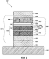
- the magnetic memory cell 100 of FIG. 1 is configured as a "top pinned" memory cell (i.e., a memory cell in which the fixed region 140 is disposed over the free region 110). However, in other embodiments, such as that of FIG. 3 , a free region 110' may overlie a fixed region 140'. Thus, with reference to FIG. 3 , a magnetic memory cell 100' including a MTJ 150' may be configured as a "bottom pinned" memory cell.
- the magnetic memory cell 100' may include a magnetic cell core 101' disposed between the lower electrode 104 and the top electrode 126.
- the magnetic memory cell 100' may include a lower intermediary region 106 overlying the lower electrode 104.
- the seed material 108 may overlie the lower intermediary region 106, if present. In other embodiments, the seed material 108 may directly overlie and contact the lower electrode 104.
- the seed material 108 may be the same as described above with reference to FIG. 1 .
- the fixed region 140' may directly overlie and contact the seed material 108.
- the fixed region 140' may include a fixed magnetic orientation, indicated by arrows 119.
- the fixed region 140' may include the same materials described above with reference to fixed region 140.
- the fixed region 140' includes a second magnetic portion 120', a coupling material 118', and a first magnetic portion 116'.
- the first magnetic portion 116' may include a first magnetic sub-region 116a', a spacer 116b', and a second magnetic sub-region 116c'.
- the first magnetic sub-region 116a', the spacer 116b', and the second magnetic sub-region 116c' may be the same as the first magnetic sub-region 116a, the spacer 116b, and the second magnetic sub-region 116c, respectively, described above with reference to FIG. 1 .
- Each of the first magnetic portion 116', the coupling material 118', and the second magnetic portion 120' may be the same as the first magnetic portion 116, the coupling material 118, and the second magnetic portion 120, respectively, described above with reference to FIG. 1 .
- the fixed region 140' may not directly overlie the tunnel barrier material 130 as in the magnetic memory cell 100 of FIG. 1 .
- the second magnetic portion 120' of the fixed region 140' may directly overlie and contact the underlying seed material 108.
- the coupling material 118' may overlie the second magnetic portion 120' and the first magnetic portion 116' may overlie the coupling material 118'.
- the tunnel barrier material 130 may overlie the fixed region 140'.
- the first portion 112 of the tunnel barrier material 130 may directly overlie and contact the fixed region 140'.
- the first portion 112 may be formed over the fixed region 140' to form an interface 111' between the fixed region 140' and the tunnel barrier material 130.
- the fixed region 140' may exhibit a crystal structure that is aligned with a crystal structure of the first portion 112.
- each of the first portion 112 and the fixed region 140' may exhibit a bcc (001) crystal structure without a change in the crystal structure of the MTJ 150' at the interface 111'.
- the tunnel barrier material 130 may include the same materials as described above with reference to FIG. 1 .
- each of the first portion 112 and the second portion 114 of the tunnel barrier material 130 may be the same as described above with reference to FIG. 1 .
- An interface 113' between the first portion 112 and the second portion 114 may be smooth and exhibit the same crystal orientation as the interface 111' on which the first portion 112 is formed.
- the tunnel barrier material 130 may be disposed directly between the fixed region 140' and the free region 110'.
- the free region 110' may directly overlie and contact the tunnel barrier material 130. In some embodiments, the free region 110' directly overlies and contacts the second portion 114 of the tunnel barrier material 130.
- the free region 110' may include the same materials as described above with reference to FIG. 1 .
- the free region 110' may include a switchable magnetic orientation, indicated by arrows 109.
- the optional upper intermediary region 124 may overlie the free region 110'.
- the upper electrode 126 may overlie the upper intermediary region 124, if present
- the memory cells of embodiments of the disclosure may be configured as "out-of-plane" STT-MRAM cells.
- "Out-of-plane" STT-MRAM cells may include magnetic regions exhibiting a magnetic orientation that is predominately oriented in a vertical direction (e.g., a direction that is perpendicular to a width and length of the respective region or a direction that is perpendicular to a primary surface of the substrate on which the STT-MRAM cell is located). For example, as illustrated in FIG. 1 and FIG.
- an STT-MRAM cell (e.g ., magnetic memory cell 100, magnetic memory cell 100') may be configured to exhibit a vertical magnetic orientation in at least one of the magnetic regions (e.g., the free region 110, 110' and the fixed region 140, 140'). As indicated in FIG. 1 and FIG. 3 , each of the free region 110, 110' and the fixed region 140, 140' may exhibit a vertical magnetic orientation as indicated by the arrows 109 and the arrows 119. The magnetic orientation of the fixed region 140, 140' may remain directed in essentially the same direction throughout use and operation of the STT-MRAM cell, for example, in the direction indicated by arrows 119.
- an in-plane magnetic memory cell 100" including a magnetic cell core 101" may be configured to exhibit a horizontal magnetic orientation in at least one of the magnetic regions (e.g., a free region 110" and a fixed region 140") of an MTJ 150", as indicated by arrow 109' in the free region 110" and arrow 119' in the fixed region 140".
- a semiconductor device may include at least one magnetic memory cell including the magnetic cell cores 101, 101', 101" of the disclosure disposed between a pair of electrodes.
- the semiconductor device comprises a magnetic tunnel junction over a seed material on a substrate, the magnetic tunnel junction exhibiting a tunnel magnetoresistance of between about 180% and about 300% and comprising a magnetic material over the seed material, an oxide material over the magnetic material, another oxide material over the oxide material, the oxide material and the another oxide material having a thickness of between about 10 ⁇ and about 20 ⁇ , and another magnetic material over the another oxide material.
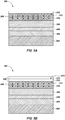
- the method may include forming a magnetic memory cell 200 over a substrate 202.
- a lower electrode material 204 is formed over the substrate 202.
- the lower electrode material may include any of the materials described above with reference to the lower electrode 104.
- An intermediary region material 206 may, optionally, be formed over the lower electrode material 204.
- the lower intermediary region material 206 may be formed from any of the materials described above with reference to the lower intermediary region 106.
- the lower intermediary region material 206 may be integral with the conductive material of the lower electrode material 204.
- the lower intermediary region material 206 may be an upper-most sub-region of the lower electrode material 204.
- a seed material 208 may be formed over the lower intermediary region material 206, if present, or the lower electrode material 204.
- the seed material 208 may be formed as described above with reference to FIG. 1 .
- Each portion of the seed material 208 may be formed by sputter deposition, such as by magnetron sputtering (e.g ., high-power impulse magnetron sputtering (HIPIMS), dc magnetron sputtering, etc.), ion-beam sputtering, or other PVD methods.
- the seed material 208 may be also formed by at least one of atomic layer deposition (ALD), chemical vapor deposition (CVD), plasma enhanced chemical vapor deposition (PECVD), low pressure chemical vapor deposition (LPCVD), or other film deposition processes.
- ALD atomic layer deposition
- CVD chemical vapor deposition
- PECVD plasma enhanced chemical vapor deposition
- LPCVD low pressure chemical vapor deposition
- a free region material 210 is formed over the seed material 208.
- the free region material 210 may be formed of any of the materials described above with reference to the free region 110.
- the free region material 210 may include a CoFeB material.
- the free region material 210 may include an artificial superlattice structure material formed of alternating portions of the magnetic material 117 and the conductive material 115, as described above with reference to the first magnetic portion 116 of FIG. 2 .
- the free region material 210 may be amorphous when formed and may be formed at a temperature such that the free region material 210 remains in an amorphous state.
- the free region material 210 may exhibit a switchable magnetic orientation, indicated by arrows 209.
- a tunnel barrier material 230 is formed over the free region material 210.
- the tunnel barrier material 230 may include a first portion 212 and a second portion 214.
- the first portion 212 of the tunnel barrier material 230 may be formed over the free region material 210 to form an interface 211.
- the first portion 212 of the tunnel barrier material 230 may be formed from the same materials as described above with reference to the first portion 112 of the tunnel barrier material 130.
- the first portion 212 may be formed by at least one of ALD, CVD, PECVD, LPCVD, PVD, or other film deposition processes.
- the first portion 212 is formed by sputter deposition, such as by magnetron sputtering (e.g., high-power impulse magnetron sputtering (HIPIMS), DC sputtering, etc.), RF sputtering, electron beam physical vapor deposition, ion-beam reactive sputtering, or other PVD methods.
- the first portion 212 is formed from MgO.
- the first portion 212 may be formed as MgO, rather than formed as a magnesium portion that is subsequently oxidized to MgO by exposing the magnesium portion to oxidizing conditions.
- the source of the MgO may be a single crystal MgO or a multi-crystal MgO deposition source or sputtering target
- the first portion 212 may be formed over the free region material 210 at a first temperature such that the underlying free region material 210 is not crystallized. In other words, the free region material 210 may remain amorphous during formation of the first portion 212 of the tunnel barrier material 230. As formed, the first portion 212 may be amorphous or crystalline. In some embodiments, the free region material 210 includes a CoFeB material that remains amorphous during formation of the first portion 212. In some embodiments, the first portion 212 is crystalline when initially formed.
- the first portion 212 may be formed at a temperature between about -150°C and about 150°C, such as between about -150°C and about 0°C, between about 0°C and about 25°C, between about 20°C and about 25°C, between about 25°C and about 50°C, or between about 50°C and about 150°C.
- the first portion 212 is formed at room temperature (e.g., between about 20°C and about 25°C). If the first portion 212 is formed at room temperature, the underlying free region material 210 may remain in its amorphous state.
- the free region material 210 and the first portion 212 are annealed, such as by thermal annealing. Exposing the free region material 210 and the first portion 212 to annealing conditions may crystallize the free region material 210 from the interface 211 through the free region material 210. After annealing the first portion 212 and the free region material 210, the free region material 210 may have a crystal structure that is aligned with (i.e., matched to) a crystal structure of the first portion 212.
- a CoFeB free region material 210 is crystallized from the interface 211 and includes the same crystal structure as the first portion 212 including MgO. Annealing the first portion 212 may also cause any oxygen vacancies within the first portion 212 to fill with oxygen, increasing the stoichiometry of the first portion 212 of the tunnel barrier material 230. By way of non-limiting example, where the first portion 212 includes MgO, annealing the first portion 212 may attract oxygen to the first portion 212, filling any oxygen vacancies that may have been formed during the low temperature formation of the first portion 212.
- the free region material 210 and the first portion 212 may be exposed to a temperature sufficient to crystalize the free region material 210 and for a sufficient amount of time. Exposing the first portion 212 to annealing conditions may increase the crystal quality of the first portion 212 upon which the second portion 214 may be subsequently formed, as described in more detail below. The annealing may also form a smooth surface of the first portion 212, upon which the second portion 214 is formed. The free region material 210 and the first portion 212 may be exposed to a temperature of between about 300°C and about 600°C for between about 60 seconds and about one hour (1 hr.).
- the free region material 210 and the first portion 212 may be exposed to a temperature of between about 300°C and about 350°C, between about 350°C and about 400°C, between about 400°C and about 500°C, or between about 500°C and about 600°C.
- the exposure time may be between about 60 seconds and about five minutes, between about 5 minutes and 15 minutes, between about 15 minutes and about 30 minutes, or between about 30 minutes and about 60 minutes.
- the second portion 214 of the tunnel barrier material 230 is formed.
- the second portion 214 may be formed directly over and in contact with the first portion 212.
- the second portion may be formed of the same materials described above with reference to the second portion 114.
- the second portion 214 is formed of the same material as the first portion 212.
- the first portion 212 of the tunnel barrier material 230 that has been annealed may act as a seed upon which the second portion 214 is formed, such that the crystal structure of the second portion 214 matches the crystal structure of the first portion 212.
- An exposed surface of the first portion 212 may be a seed upon which the second portion 214 is formed to the same crystal orientation as the first portion 212 and the free region material 210.
- the first portion 212 and the second portion 214 may exhibit the same crystal orientation at an interface 213.
- the second portion 214 of the tunnel barrier material 230 is formed at a second temperature that is higher than the first temperature at which the first portion 212 is formed.
- the second portion 214 may be formed by one of the same methods described above for forming the first portion 212.
- the second portion 214 may be formed by sputter deposition, such as by at least one of ALD, CVD, PECVD, LPCVD, PVD, or other film deposition processes.
- the second portion 214 is formed by sputter deposition, such as by magnetron sputtering (e.g., high-power impulse magnetron sputtering (HIPIMS), DC sputtering, etc.), RF sputtering, electron beam physical vapor deposition, ion-beam reactive sputtering, or other PVD methods.
- the second portion 214 is formed at a different, higher temperature than the first portion 212 is formed.
- the second portion 214 may be formed at a temperature between about 300°C and about 600°C, as described above.
- the second portion 214 may be formed at the same temperature as the temperature at which the first portion 212 and the free region material 210 are annealed.
- the second portion 214 may be formed at a different temperature than the temperature at which the first portion 212 and the free region material 210 are annealed.
- the second portion 214 may be formed at a temperature between about 300°C and about 600°C, such as between about 300°C and about 350°C, between about 350°C and about 400°C, between about 400°C and about 500°C, or between about 500°C and about 600°C. Forming the second portion 214 at an elevated temperature may form a more stoichiometric material having an increased crystal quality.
- the second portion 214 may include a stoichiometric amount of oxygen with less oxygen vacancies and less interstitial oxygen than the first portion 212.
- each of the first portion 212 and the second portion 214 have a ratio of magnesium to oxygen of approximately one to one.
- the second portion 214 may be formed to the same thickness, a greater thickness, or a lesser thickness than the first portion 212. In some embodiments, the ratio is about 1.5 and the total thickness of the tunnel barrier material 130 is about 18 ⁇ . The ratio of the thickness of the first portion 212 to the second portion 214 may be tailored to increase the TMR and decrease the RA of the tunnel barrier material 230.
- the tunnel barrier material 230 may be formed to exhibit a TMR of between about 180% and about 600% and an RA of between about 3 ohm ⁇ m 2 and about 8 ohm ⁇ m 2 , as described above with reference to the tunnel barrier material 130. In some embodiments, the thickness of the second portion 214 is less than a thickness of the first portion 212.
- a fixed region material 240 is formed over the second portion 214 of the tunnel barrier material 230.
- the fixed region material 240 may include a first magnetic material 216 over the second portion 214 of the tunnel barrier material 230, a coupling material 218 over the first magnetic material 216, and a second magnetic material 220 over the coupling material 218.
- the first magnetic material 216 may include a first magnetic sub-region 216a, a spacer material 216b, and a second magnetic sub-region 216c.
- Each of the first magnetic sub-region 216a, the spacer material 216b, and the second magnetic sub-region 216c may be formed of the same materials as the first magnetic sub-region 116a, the spacer 116b, and the second magnetic sub-region 116c, respectively, described above.
- Each of the first magnetic material 216, the coupling material 218, and the second magnetic material 220 may be formed of the same materials as the first magnetic portion 116, the coupling material 118, and the second magnetic portion 120, respectively, described above.
- the first magnetic material 216 and the second magnetic material 220 of the fixed region material 240 may include a fixed magnetic orientation, indicated by arrows 219.
- the coupling material 218 may be formed over the first magnetic material 216 (e.g., over the second magnetic sub-region 216c of the first magnetic material 216).
- the coupling material 218 may be formed between the first magnetic material 216 and the second magnetic material 220.
- the coupling material 218 may be formed by at least one of ALD, CVD, PVD, PECVD, LPCVD, or other film deposition processes.
- the second magnetic material 220 may be formed directly over the coupling material 218.
- the second magnetic material 220 may be formed in the same manner and from the same materials as the first magnetic material 216.
- An upper intermediary region material 224 may optionally be formed over the second magnetic material 220 and may include the same materials as the lower intermediary region material 206.
- An upper electrode material 226 is formed over the upper intermediary region material 224, if present, or over the second magnetic material 220.
- the upper electrode material 226 may be formed of the same materials as described above with reference to the upper electrode 126.
- the magnetic memory cell 200 may be processed to form the magnetic memory cell 100 as shown in FIG. 1 .
- the magnetic memory cell 200 structure may be processed by conventional photolithography, material removal, etching, or other processes that are not described in detail herein.
- the magnetic memory cell 100 described with reference to FIG. 5A through FIG. 5C describes forming the magnetic memory cell 100 of FIG. 1
- the magnetic memory cell 100' of FIG. 3 may be formed by similar methods.
- the fixed region material 240 would be formed over the seed material 208
- the first portion 212 of the tunnel barrier material 230 would be formed over the fixed region material 240
- the free region material 210 would be formed over the second portion 214 of the tunnel barrier material 230, resulting in the magnetic memory cell of FIG. 3
- the magnetic memory cell 100" of FIG. 4 may be formed by forming the free region material 210 and the fixed region material 240 to exhibit a horizontal magnetic orientation.
- Forming the tunnel barrier material 230 from the first portion 212 and the second portion 214 may increase the TMR and decrease the RA of the magnetic tunnel junction.
- the MTJ 150 may be substantially free of defects such as oxygen vacancies or interstitial oxygen within the crystal structure of the tunnel barrier material 230.
- the tunnel barrier material 230 may, therefore, exhibit improved tunneling characteristics at a high TMR and a low RA.
- a method of forming a semiconductor device comprises forming a magnetic material over an electrode on a substrate, forming a first tunnel barrier material over the magnetic material, annealing the magnetic material and the first tunnel barrier material, forming a second tunnel barrier material over the annealed first tunnel barrier material, forming another magnetic material over the second tunnel barrier material, and forming another electrode over the another magnetic material.
- a method of forming a magnetic tunnel junction comprises forming at a first temperature a barrier material over a magnetic material, annealing the barrier material and the magnetic material, forming at a second temperature another barrier material over the annealed barrier material, and forming another magnetic material over the another barrier material.
- a method of forming a semiconductor device comprises forming a seed material over a substrate, forming a magnetic material over the seed material, forming at a first temperature an oxide material over the magnetic material, forming at a second temperature higher than the first temperature, another oxide material over the oxide material, and forming another magnetic material over the another oxide material.
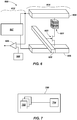
- an STT-MRAM system 600 that includes peripheral devices 612 in operable communication with an STT-MRAM cell 614, a grouping of which may be fabricated to form an array of memory cells in a grid pattern including a number of rows and columns, or in various other arrangements, depending on the system requirements and fabrication technology.
- the STT-MRAM cell 614 may include a magnetic cell core 601, an access transistor 603, a conductive material that may function as a data/sense line 604 (e.g., a bit line), a conductive material that may function as an access line 605 (e.g., a word line) and a conductive material that may function as a source line 606.
- the peripheral devices 612 of the STT-MRAM system may include read/write circuitry 607, a bit line reference 608, and a sense amplifier 609.
- the magnetic cell core 601 may be any one of the magnetic cell cores 101, 101', 101" described above. Due to the structure of the cell core 601, the method of fabrication, or both, the STT-MRAM cell 614 may have a high TMR and a low resistance (e.g., low RA product).
- an STT-MRAM cell 614 In use and operation, when an STT-MRAM cell 614 is selected to be programmed, a programming current is applied to the STT-MRAM cell 614, and the current is spin-polarized by the fixed region of the magnetic cell core 601 and exerts a torque on the free region of the cell core 601, which switches the magnetization of the free region to "write to" or "program” the STT-MRAM cell 614. In a read operation of the STT-MRAM cell 614, a current is used to detect the resistance state of the magnetic cell core 601.
- the read/write circuitry 607 may generate a write current (i.e ., a programming current) to the data/sense line 604 and the source line 606.
- a write current i.e ., a programming current
- the polarity of the voltage between the data/sense line 604 and the source line 606 determines the switch in magnetic orientation of the free region in the magnetic cell core 601.
- the free region is magnetized according to the spin polarity of the programming current and the programmed logic state is written to the STT-MRAM cell 614.
- the read/write circuitry 607 To read the STT-MRAM cell 614, the read/write circuitry 607 generates a read voltage to the data/sense line 604 and the source line 606 through the cell core 601 and the access transistor 603.
- the programmed state of the STT-MRAM cell 614 relates to the electrical resistance across the cell core 601, which may be determined by the voltage difference between the data/sense line 604 and the source line 606. In some embodiments, the voltage difference may be compared to the bit line reference 608 and amplified by the sense amplified 609.
- FIG. 6 illustrates one example of a STT-MRAM system 600 including at least one magnetic memory cell. It is contemplated, however, that the magnetic cell cores 101, 101', 101" may be incorporated and utilized within any STT-MRAM system configured to incorporate a magnetic cell core having magnetic regions. It is also contemplated that the magnetic cell cores 101, 101', 101" may be used in other magnetic memory cells besides STT-MRAM cells.
- the semiconductor device 700 includes a memory array 702 and a control logic component 704.
- the memory array 702 may include a plurality of STT-MRAM cells 614 ( FIG. 6 ) including any of the magnetic cell cores (e.g., the magnetic cell cores 101, 101', 101" of FIG. 1 , FIG. 3 , and FIG. 4 , respectively) discussed above, which magnetic cell cores (e.g., the magnetic cell cores 101, 101', 101") may have been formed according to a method described above and may be operated according to a method described above.
- the control logic component 704 may be configured to operatively interact with the memory array 702 so as to read from or write to any or all memory cells (e.g., STT-MRAM cell 614 ( FIG. 6 )) within the memory array 702.
- the semiconductor device comprises an array of magnetic cell structures, each magnetic cell structure comprising a magnetic tunnel junction over an electrode on a substrate, each magnetic tunnel junction comprising a magnetic material over the substrate, a first tunnel barrier material over the magnetic material, a second tunnel barrier material over the first tunnel barrier material, and another magnetic material over the second tunnel barrier material, each magnetic tunnel junction configured to exhibit a tunnel magnetoresistance of between about 180% and about 600% at a resistance area product of less than about 8 ohm ⁇ m 2 .
- the semiconductor device further comprises another electrode over the another magnetic material.
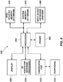
- the processor-based system 800 may include various electronic devices manufactured in accordance with embodiments of the present disclosure.
- the processor-based system 800 may be any of a variety of types such as a computer, pager, cellular phone, personal organizer, control circuit, or other electronic device.
- the processor-based system 800 may include one or more processors 802, such as a microprocessor, to control the processing of system functions and requests in the processor-based system 800.
- the processor 802 and other subcomponents of the processor-based system 800 may include magnetic memory devices manufactured in accordance with embodiments of the present disclosure.
- the processor-based system 800 may include a power supply 804 in operable communication with the processor 802.
- the power supply 804 may include one or more of a fuel cell, a power scavenging device, permanent batteries, replaceable batteries, and rechargeable batteries.
- the power supply 804 may also include an AC adapter; therefore, the processor-based system 800 may be plugged into a wall outlet, for example.
- the power supply 804 may also include a DC adapter such that the processor-based system 800 may be plugged into a vehicle cigarette lighter or a vehicle power port, for example.
- a user interface 806 may be coupled to the processor 802.
- the user interface 806 may include input devices such as buttons, switches, a keyboard, a light pen, a mouse, a digitizer and stylus, a touch screen, a voice recognition system, a microphone, or a combination thereof.
- a display 808 may also be coupled to the processor 802.
- the display 808 may include an LCD display, an SED display, a CRT display, a DLP display, a plasma display, an OLED display, an LED display, a three-dimensional projection, an audio display, or a combination thereof.
- an RF sub-system/baseband processor 810 may also be coupled to the processor 802.
- the RF sub-system/baseband processor 810 may include an antenna that is coupled to an RF receiver and to an RF transmitter (not shown).
- a communication port 812, or more than one communication port 812, may also be coupled to the processor 802.
- the communication port 812 may be adapted to be coupled to one or more peripheral devices 814, such as a modem, a printer, a computer, a scanner, or a camera, or to a network, such as a local area network, remote area network, intranet, or the Internet, for example.
- the processor 802 may control the processor-based system 800 by implementing software programs stored in the memory.
- the software programs may include an operating system, database software, drafting software, word processing software, media editing software, or media playing software, for example.
- the memory is operably coupled to the processor 802 to store and facilitate execution of various programs.
- the processor 802 may be coupled to system memory 816, which may include one or more of spin torque transfer magnetic random access memory (STT-MRAM), magnetic random access memory (MRAM), dynamic random access memory (DRAM), static random access memory (SRAM), racetrack memory, and other known memory types.
- STT-MRAM spin torque transfer magnetic random access memory
- MRAM magnetic random access memory
- DRAM dynamic random access memory
- SRAM static random access memory
- racetrack memory racetrack memory
- the system memory 816 may include volatile memory, non-volatile memory, or a combination thereof.
- the system memory 816 is typically large so that it can store dynamically loaded applications and data.
- the system memory 816 may include semiconductor devices, such as the semiconductor device 700 of FIG. 7 , memory cells including any of the magnetic cell cores 101, 101', 101" of FIG. 1 , FIG. 3 , and FIG. 4 , respectively, described above, or a combination thereof.
- the processor 802 may also be coupled to non-volatile memory 818, which is not to suggest that system memory 816 is necessarily volatile.
- the non-volatile memory 818 may include one or more of STT-MRAM, MRAM, read-only memory (ROM) such as an EPROM, resistive read-only memory (RROM), and flash memory to be used in conjunction with the system memory 816.
- ROM read-only memory
- RROM resistive read-only memory
- flash memory to be used in conjunction with the system memory 816.
- the size of the non-volatile memory 818 is typically selected to be just large enough to store any necessary operating system, application programs, and fixed data.
- the non-volatile memory 818 may include a high capacity memory such as disk drive memory, such as a hybrid-drive including resistive memory or other types of non-volatile solid-state memory, for example.
- the non-volatile memory 818 may include semiconductor devices, such as the semiconductor device 700 of FIG. 7 , memory cells including any of the magnetic cell cores 101, 101', 101" of FIG. 1 , FIG. 3 , and FIG. 4 , respectively, or a combination thereof.
- FIG. 9 is a graphical representation comparing the TMR vs. the RA of MTJs formed according to the present invention to MTJs formed by conventional methods.
- a MgO tunnel barrier material was formed by RF sputtering at about 20°C over a CoFeB magnetic material. The MgO and the CoFeB were annealed at a temperature of about 500°C to crystallize the CoFeB magnetic material in the same crystal orientation as the MgO.
- a second MgO tunnel barrier material was formed by RF sputtering at about 500°C over the annealed MgO. Another CoFeB magnetic material was formed over the second MgO tunnel barrier material.
- a tantalum material was formed over the CoFeB magnetic material and a cobalt/palladium magnetic material was formed over the tantalum to complete the MTJ structure.
- a conventional MTJ was formed by forming an MgO tunnel barrier material over a CoFeB magnetic material at room temperature. The MgO and the CoFeB were annealed at a temperature of about 500°C. Another CoFeB magnetic material was formed over the MgO.
- the TMR and the RA of the MTJ structures were measured using conventional techniques.
- the upper left line of FIG. 9 shows the TMR and the RA of MTJs formed according to embodiments of the disclosure and the lower right line shows the TMR and the RA of the MTJs formed by conventional methods. As shown in the graph, the MTJs formed by the methods disclosed herein exhibit a higher TMR at a lower RA than MTJs formed by conventional methods.
- FIG. 10 is a graphical representation of the TMR vs. the RA of MTJs formed according to the present invention.
- a first MgO tunnel barrier material was formed to a first thickness ("X") over a CoFeB magnetic material.
- the MgO was formed by RF sputtering at about 20°C.
- the MgO and the CoFeB were annealed at a temperature of about 500°C to crystallize the CoFeB in the same crystal orientation as the MgO.
- a second MgO tunnel barrier material was formed by RF sputtering at about 500°C over the annealed MgO.
- the second MgO tunnel barrier material was formed to a second thickness ("Y").
- FIG. 10 graphs the TMR and the RA of MTJs having different ratios of the thickness of the first MgO tunnel barrier material to the thickness of the second MgO tunnel barrier material ( i.e ., X/Y). Accordingly, the ratio of X/Y may be tailored to form a MTJ exhibiting a desired TMR at a desired RA.
Description
- Embodiments disclosed herein relate to semiconductor devices including magnetic memory cells having a magnetic tunnel junction and methods of forming such devices and magnetic tunnel junctions. More specifically, embodiments disclosed herein relate to magnetic tunnel junctions exhibiting a low resistance area product at a high tunnel magnetoresistance, semiconductor devices including the magnetic tunnel junctions, and methods of forming the magnetic tunnel junctions and semiconductor devices.
- Magnetic Random Access Memory (MRAM) is a non-volatile memory technology based on magnetoresistance. One type of MRAM is spin torque transfer MRAM (STT-MRAM), in which a magnetic cell core includes a magnetic tunnel junction ("MTJ") sub-structure with at least two magnetic regions, for example, a "fixed region" and a "free region," with anon-magnetic region (e.g., a tunnel barrier material) between. The free region and the fixed region may exhibit magnetic orientations that are either horizontally oriented ("in-plane") or perpendicularly oriented ("out-of-plane") relative to the thickness of the regions. The fixed region includes a magnetic material that has a substantially fixed (e.g., a non-switchable) magnetic orientation. The free region, on the other hand, includes a magnetic material that has a magnetic orientation that may be switched, during operation of the cell, between a "parallel" configuration and an "anti-parallel" configuration. In the parallel configuration, the magnetic orientations of the fixed region and the free region are directed in the same direction (e.g., north and north, east and east, south and south, or west and west, respectively). In the "anti-parallel" configuration, the magnetic orientations of the fixed region and the free region are directed in opposite directions (e.g., north and south, east and west, south and north, or west and east, respectively). In the parallel configuration, the STT-MRAM cell exhibits a lower electrical resistance across the magnetoresistive elements (e.g., the fixed region and free region), defining a "0" logic state of the MRAM cell. In the anti-parallel configuration, the STT-MRAM cell exhibits a higher electrical resistance across the magnetoresistive elements, defining a "1" logic state of the STT-MRAM cell.
- Switching of the magnetic orientation of the free region may be accomplished by passing a programming current through the magnetic cell core, including the fixed and free regions. The fixed region polarizes the electron spin of the programming current, and torque is created as the spin-polarized current passes through the core. The spin-polarized electron current exerts the torque on the free region. When the torque of the spin-polarized electron current is greater than a critical switching current density (J c ) of the free region, the direction of the magnetic orientation of the free region is switched. Thus, the programming current can be used to alter the electrical resistance across the magnetic regions. The resulting high or low electrical resistance states across the magnetoresistive elements enable the write and read operations of the MRAM cell. After switching the magnetic orientation of the free region to achieve the one of the parallel configuration and the anti-parallel configuration associated with a desired logic state, the magnetic orientation of the free region is usually desired to be maintained, during a "storage" stage, until the MRAM cell is to be rewritten to a different configuration (i.e., to a different logic state).
- Switching of the magnetic orientation of the free region of a magnetic memory cell including a MTJ may be affected by the tunnel magnetoresistance ("TMR") and the resistance area product ("RA") of the cell. The TMR of a MTJ is a function of the resistance between a top electrode and a bottom electrode, between which the MTJ is disposed, in the high electrical resistance state and the low electrical resistance state. Specifically, the TMR measures the difference between a cell's electrical resistance in the anti-parallel configuration (Rap) and its electrical resistance in the parallel configuration (Rp) to Rp (i.e., TMR = (Rap - Rp)/Rp). Thus, the TMR is equivalent to the change in resistance observed by changing the magnetic state of the free layer. Generally, a MTJ with a homogeneous crystal structure (e.g., a bcc (001) crystal structure), having few structural defects in the microstructure of its magnetic material, has a higher TMR than a MTJ with structural defects. A cell with high TMR may have a high read-out signal, which may speed the reading of the MRAM cell during operation. A higher TMR is preferred for reliable read operation as it will generate a larger signal difference between the on and off states of the cell. In other words, the higher the TMR, the more sensitive the device, and the easier to distinguish logic states of an associated memory cell.
- Another significant characteristic of a magnetic memory cell core includes the RA. The RA of a magnetic memory cell is an indication of the voltage used to switch the magnetic orientation of the free region during programming (e.g., the threshold switching voltage). An increase in the RA of a magnetic memory cell may degrade the performance of the cell by utilizing a higher threshold switching voltage, reducing the usable life of the cell. The RA may be decreased by decreasing a thickness of the tunnel barrier material. However, decreasing the thickness of the tunnel barrier material may also decrease the TMR. Thus, although a high TMR and a low RA are desired, in general, an increase in the TMR of a MTJ is obtained at the expense of a higher RA. A conventional MTJ exhibits a TMR of less than about 120% at an RA of greater than about 4 ohm µm2.
- Efforts to increase the TMR of a MTJ while maintaining a low RA include attempts to reduce structural defects in the crystal structure of the MTJ. For example, a magnesium oxide tunnel barrier material may be formed at elevated temperatures to produce the tunnel barrier material having stoichiometric proportions and minimal oxygen vacancies or interstitial oxygen. However, the elevated temperatures may undesirably cause an underlying magnetic material to crystalize in an undesired crystal orientation. A mismatch in crystal orientation of the magnetic material and the tunnel barrier material undesirably increases the RA and decreases the TMR of the MTJ. The increase in the RA increases the voltage required to switch the magnetic orientation of the free region during programming, increases the junction resistance, and increases the threshold switching voltage of the device. A decrease in the TMR reduces the effective spin-polarization of the electrons as they pass through the MTJ, reducing tunneling through the MTJ.
- Alternatively, the tunnel barrier material may be formed at lower temperatures. However, when the tunnel barrier material is formed at lower temperatures, defects, such as oxygen vacancies and interstitial oxygen atoms, within the tunnel barrier material increase. The atomic defects in the tunnel barrier material may degrade device performance by causing electrons to scatter as they travel through the MTJ and reducing the TMR of the MTJ.
-
EP 1 801 895 A2 discloses a method in which an improved tunneling barrier layer is formed for use in a MTJ device. This is accomplished by forming the tunneling barrier layer in two steps. First a layer of magnesium is deposited by DC sputtering and converted to magnesium oxide through radical oxidation. This is followed by a second, thinner, magnesium layer that is converted to magnesium oxide through normal oxidation. Optionally, there may also be a thin layer of magnesium on the two magnesium oxide layers. The tunneling barrier layer is located between pinned ferrromagnetic layer and free ferromagnetic layer. -
JP 2010-087355 A US 2010/328822 A1 describes a method and system for providing a barrier for a magnetoresistive structure utilizing heating.US 2003/228710 A1 describes a multilayer dielectric tunnel barrier used in magnetic tunnel junction devices, and its method of fabrication. -
-
FIG. 1 is a simplified cross-sectional view of a magnetic cell structure according to an embodiment of the disclosure; -
FIG. 2 is a simplified cross-sectional view of a magnetic material including alternating portions of a magnetic material and a conductive material; -
FIG. 3 is a simplified cross-sectional view of a magnetic cell structure according to another embodiment of the disclosure; -
FIG. 4 is a simplified cross-sectional view of a magnetic cell structure according to an embodiment of the present disclosure, wherein the fixed region and the free region exhibit in-plane magnetic orientations; -
FIGS. 5A through FIG. 5C are simplified cross-sectional views illustrating different process stages for a method according to the present invention for forming the magnetic cell structure ofFIG. 1 ; -
FIG. 6 is a schematic of an STT-MRAM system including a memory cell having a magnetic cell structure according to an embodiment of the disclosure; -
FIG. 7 is a simplified block diagram of a semiconductor device including memory cells having a magnetic cell structure according to an embodiment of the present disclosure; -
FIG. 8 is a simplified block diagram of a system implemented according to one or more embodiments of the present disclosure; -
FIG. 9 is a graphical representation comparing the TMR vs. the RA of magnetic tunnel junctions formed according to embodiments of the present disclosure and magnetic tunnel junctions formed by conventional methods; and -
FIG. 10 is a graphical representation of the TMR vs. the RA of magnetic tunnel junctions formed according to embodiments of the present disclosure. - The illustrations included herewith are not meant to be actual views of any particular systems or semiconductor structures, but are merely idealized representations that are employed to describe embodiments described herein. Elements and features common between figures may retain the same numerical designation.
- The following description provides specific details, such as material types, material thicknesses, and processing conditions in order to provide a thorough description of embodiments described herein. However, a person of ordinary skill in the art will understand that the embodiments disclosed herein may be practiced without employing these specific details. Indeed, the embodiments may be practiced in conjunction with conventional fabrication techniques employed in the semiconductor industry. In addition, the description provided herein does not describe a complete process flow for manufacturing semiconductor devices, magnetic tunnel junctions, or magnetic memory cells, and the semiconductor devices, magnetic tunnel junctions, and magnetic memory cells described below do not form a complete semiconductor device, magnetic tunnel junction, or magnetic memory cell. Only those process acts and structures necessary to understand the embodiments described herein are described in detail below. Additional acts to form a complete semiconductor device and a magnetic memory cell including the semiconductor device may be performed by conventional techniques.
- The present invention is embodied by a method of forming a magnetic device according to the independent claim 1. Further advantageous features are set out in the dependent claims. A semiconductor device may include a magnetic cell structure comprising a MTJ. The MTJ may include a tunnel barrier material disposed between adjacent magnetic materials. A magnetic material may overlie a substrate and the tunnel barrier material may overlie the magnetic material. Another magnetic material may overlie the tunnel barrier material. The tunnel barrier material may exhibit the same crystal orientation as the adjacent magnetic materials. The semiconductor device including the MTJ may exhibit a high TMR, such as greater than about 180%, at a low RA, such as at less than about 8 ohm µm2.
- The tunnel barrier material formed according to the present invention includes at least two portions. A first portion of the tunnel barrier material is formed over the magnetic material at a first temperature. The first portion of the tunnel barrier material and the magnetic material are annealed, particularly to crystallize the magnetic material and orient the crystal structure of the magnetic material in alignment with the crystal structure of the first portion of the tunnel barrier material. The magnetic material and the first portion of the tunnel barrier material may be annealed at a temperature between about 300°C and about 600°C for an amount of time sufficient to crystallize the magnetic material. After annealing, a second portion of the same tunnel barrier material is formed over the first portion at a second temperature, which is higher than the first temperature at which the first portion of the tunnel barrier material is formed. The tunnel barrier material including the first portion and the second portion may exhibit a higher TMR, such as greater than about 180%, at a low RA, such as at less than about 8 ohm µm2, than a conventional tunnel barrier material. The tunnel barrier material may also be thicker and exhibit the higher TMR than a conventional tunnel barrier material, while maintaining the low RA. In some embodiments, the RA of the tunnel barrier material is between about 4 ohm µm2 and about 8 ohm µm2 and the TMR of the tunnel barrier material is between about 180% and about 205%.
- Referring to
FIG. 1 , amagnetic memory cell 100 including amagnetic cell core 101 according to some embodiments is illustrated. Themagnetic cell core 101 may include amagnetic tunnel junction 150 and may be disposed between alower electrode 104 and anupper electrode 126 over asubstrate 102. TheMTJ 150 may include a magnetic region and another magnetic region, for example, a "free region 110" and a "fixed region" 140, respectively. Atunnel barrier material 130 may be disposed between thefree region 110 and the fixedregion 140. - The
substrate 102 may include a base material or other construction upon which components, such as those within memory cells, are formed. Thesubstrate 102 may be a semiconductor substrate, a base semiconductor material on a supporting substrate, a metal electrode, or a semiconductor substrate having one or more materials, structures, or regions formed thereon. Thesubstrate 102 may be a conventional silicon substrate or other bulk substrate including semiconductor material. As used herein, the term "bulk substrate" means and includes not only silicon wafers, but also silicon-on-insulator ("SOI") substrates, such as silicon-on-sapphire ("SOS") substrates or silicon-on-glass ("SOG") substrates, epitaxial layers of silicon on a base semiconductor foundation, or other semiconductor or optoelectronic materials, such as silicon-germanium (Si1-xGex, where x is, for example, a mole fraction between 0.2 and 0.8), germanium (Ge), gallium arsenide (GaAs), gallium nitride (GaN), or indium phosphide (InP), among others. Furthermore, when reference is made to a "substrate" in the following description, previous process stages may have been utilized to form materials, regions, or junctions in the base semiconductor structure or foundation. - The
lower electrode 104 may overlie thesubstrate 102. Thelower electrode 104 may include a metal such as copper, tungsten, platinum, palladium, titanium, tantalum, nickel, titanium nitride (TiN), tantalum nitride (TaN), tungsten nitride (WN), polysilicon, a metal silicide, a metal alloy, or combinations thereof. - One or more lower
intermediary regions 106 may, optionally, be disposed under the magnetic regions (e.g., thefree region 110 and the fixed region 140). The lowerintermediary region 106, if included, may be configured to inhibit diffusion of species between thelower electrode 104 and materials overlying thelower electrode 104. The lowerintermediary region 106 may include a conductive material such as one or more of copper, tantalum, titanium, tungsten, ruthenium, tantalum nitride, and titanium nitride. - A
seed material 108 may overlie the lowerintermediary region 106, if present, or thelower electrode 104 if the lowerintermediary region 106 is not present Theseed material 108 may include tantalum, platinum, ruthenium, iron, nickel, cobalt, chromium, titanium, zirconium, vanadium, copper, zinc, rhodium, silver, hafnium, tungsten, iridium, tantalum nitride, and combinations thereof. By way of non-limiting example, theseed material 108 may include tungsten and at least one of iron, cobalt, nickel, or another suitable material. In other embodiments, theseed material 108 may include iron and cobalt and may further include at least one transition element, such as tantalum, platinum, ruthenium, nickel, chromium, titanium, zirconium, vanadium, copper, zinc, rhodium, silver, hafnium, and tungsten. In yet other embodiments, theseed material 108 may include at least one of hafnium, zirconium, and tantalum and at least one of iron, cobalt, and nickel, such as FeHf. Theseed material 108 may be a homogeneous composition of theseed material 108 or may include distinct portions of one or more of tantalum, platinum, ruthenium, iron, nickel, cobalt, chromium, titanium, zirconium, vanadium, copper, zinc, rhodium, silver, hafnium, tungsten, and iridium adjacent to a distinct portion of another of tantalum, platinum, ruthenium, iron, nickel, cobalt, chromium, titanium, zirconium, vanadium, copper, zinc, rhodium, silver, hafnium, tungsten, and iridium. - The
free region 110 may overlie theseed material 108. In some embodiments, thefree region 110 directly overlies and contacts theseed material 108. Thefree region 110 may include a magnetic material exhibiting a switchable magnetic orientation, indicated byarrows 109, during use and operation of themagnetic memory cell 100. The switchable magnetic orientation may be switched between a parallel configuration and an anti-parallel configuration by the application of a current or applied field to themagnetic memory cell 100. - In some embodiments, the
free region 110 may be a conventional free region. In other embodiments, thefree region 110 may include alternating portions of a magnetic material and a conductive material. However, thefree region 110 is not so limited and may include other suitable magnetic materials that exhibit a switchable magnetic orientation. - In some embodiments, the
free region 110 may include a ferromagnetic material including at least one of cobalt (Co) and iron (Fe) (e.g., CoxFey, wherein x = 10 to 80 and y = 10 to 80) and, in some embodiments, also boron (B) (e.g., CoxFeyBz, wherein x = 10 to 80, y = 10 to 80, and z = 0 to 50). Thus, thefree region 110 may include at least one of Co, Fe, and B (e.g., a CoFeB material, a CoFe material, a FeB material, a CoB material, etc.). As used herein, the term "CoFeB material" means and includes a material comprising cobalt, iron, and boron (e.g., CoxFeyBz, wherein x = 10 to 80, y = 10 to 80, and z = 0 to 50). A CoFeB material may or may not exhibit magnetism, depending on its configuration (e.g., its thickness). In other embodiments, thefree region 110 may alternatively or additionally include nickel (Ni) (e.g., an NiB material). In some embodiments, thefree region 110 may be substantially free of boron and may include, for example, CoFe. The CoFe may be formed as CoFeB and the boron may be diffused out of thefree region 110 after formation thereof, or the CoFe may be formed (e.g., deposited) as CoFe, without any boron. - The
free region 110 may be homogeneous, or may include one or more sub-regions (e.g., a CoFeB material, with sub-regions having different relative atomic ratios of Co, Fe, and B). - A
tunnel barrier material 130 may overlie thefree region 110. In some embodiments, thetunnel barrier material 130 directly overlies and contacts thefree region 110. Thetunnel barrier material 130 may include a nonmagnetic, crystalline material, such as magnesium oxide (MgO), aluminum oxide (Al2O3), titanium dioxide (TiO2), tantalum oxide (Ta2O5), ruthenium oxide (RuO2), boron oxide (B2O3), or combinations thereof. Thetunnel barrier material 130 may be configured to induce interfacial magnetic anisotropy in thefree region 110 and the fixedregion 140 and may also be configured to function as a tunnel region of theMTJ 150 effected by interaction of thefree region 110, thetunnel barrier material 130, and the fixedregion 140. - The
tunnel barrier material 130 may include afirst portion 112 and asecond portion 114. Thefirst portion 112 may overlie thefree region 110. In some embodiments, thefirst portion 112 directly overlies and contacts thefree region 110. Thefirst portion 112 may be formed over thefree region 110 to form aninterface 111 between thefree region 110 and thetunnel barrier material 130. A crystal orientation of theMTJ 150 may not change at theinterface 111 between thefirst portion 112 and thefree region 110. By way of example and not limitation, each of thefree region 110 and thefirst portion 112 may exhibit a bcc (001) crystal structure. As described in more detail below, each of thefirst portion 112 and thefree region 110 may be amorphous (e.g., not crystalline) as formed, with the desired crystal structure occurring following an anneal. In some embodiments, thefirst portion 112 is an oxide material and may include MgO, Al2O3, TiO2, Ta2O5, RuO2, B2O3, or combinations thereof. - The
second portion 114 may overlie thefirst portion 112. In some embodiments, thesecond portion 114 directly overlies and contacts thefirst portion 112. Aninterface 113 between thefirst portion 112 and thesecond portion 114 may be smooth and exhibit the same crystal orientation as thefirst portion 112 and the free region 110 (e.g., a bcc (001) crystal structure). Thesecond portion 114 may be an oxide material and may include MgO, Al2O3, TiO2, Ta2O5, RuO2, B2O3, or combinations thereof. Thefirst portion 112 and thesecond portion 114 may include the same material. In some embodiments, thefirst portion 112 and thesecond portion 114 include MgO. In some such embodiments, thesecond portion 114 includes a ratio of oxygen to magnesium closer to stoichiometric (e.g., 1:1) than thefirst portion 112. Thus, thesecond portion 114 may have less oxygen vacancies and less interstitial oxygen and also a higher density than thefirst portion 112. Thesecond portion 114 may exhibit less structural defects than thefirst portion 112 and, in some embodiments, may exhibit a higher TMR and a lower RA than thefirst portion 112. - The
tunnel barrier material 130 may have a total thickness (i.e., a sum of a thickness of thefirst portion 112 and a thickness of the second portion 114) of between about 10 Å and about 30 Å, such as between about 10 Å and about 15 Å, between about 15 Å and about 20 Å, between about 20 Å and about 25 Å, or between about 25 Å and about 30 Å Thetunnel barrier material 130 may have a thickness of between about 10 Å and about 20 Å. In some embodiments, the thickness of thetunnel barrier material 130 is about 18 Å - The
first portion 112 and thesecond portion 114 may have the same thickness, thefirst portion 112 may have a greater thickness than thesecond portion 114, or thesecond portion 114 may have a greater thickness than thefirst portion 112. The RA and the TMR of theMTJ 150 may be tailored by altering the thickness of thefirst portion 112 relative to the thickness of thesecond portion 114 of thetunnel junction material 130. A ratio of the thickness of thefirst portion 112 to the thickness of thesecond portion 114 may be between about 0.9 and about 2.0, such as between about 0.9 and about 1.0, between about 1.0 and about 1.25, between about 1.25 and about 1.5, between about 1.2 and about 1.8, or between about 1.5 and about 2.0. In some embodiments, the ratio is between about 1.0 and about 1.5 and the total thickness of thetunnel barrier material 130 is about 18 Å. - The
tunnel barrier material 130 having thefirst portion 112 and thesecond portion 114 may exhibit a TMR of between about 180% and about 600%, such as between about 180% and about 200%, between about 180% and about 225%, between about 180% and about 300%, between about 200% and about 220%, between about 220% and about 250%, between about 250% and about 300%, between about 300% and about 400%, or between about 400% and about 600%. In some embodiments, the TMR is between about 180% and about 300%. Thetunnel barrier material 130 may exhibit a RA of between about 3 ohm µm2 and about 8 ohm µm2, such as between about 3 ohm µm2 and about 4 ohm µm2, between about 4 ohm µm2 and about 5 ohm µm2, between about 5 ohm µm2 and about 6 ohm µm2, between about 6 ohm µm2 and about 7 ohm µm2, or between about 7 ohm µm2 and about 8 ohm µm2. In some embodiments, the RA is between about 6 ohm µm2 and about 7 ohm µm2. In other embodiments, thetunnel barrier material 130 exhibits an RA of between about 4 ohm µm2 and about 8 ohm µm2 and a TMR of between about 180% and about 205%. By way of non-limiting example, thetunnel barrier material 130 may exhibit a RA of about 4 ohm µm2 and a TMR of about 180%, or a RA of about 8 ohm µm2 and a TMR of about 205% at a thickness of between about 10 Å and about 20 Å. - The fixed
region 140 may overlie thetunnel barrier material 130. In some embodiments, the fixedregion 140 directly overlies and contacts thesecond portion 114 of thetunnel barrier material 130. - The fixed
region 140 may include one or more magnetic materials and, optionally, one or more non-magnetic materials. For example, the fixedregion 140 may be configured as a synthetic antiferromagnet including a sub-region of ruthenium or tantalum adjoined by magnetic sub-regions. The magnetic sub-regions may include a material including cobalt, and at least one of palladium and platinum, and combinations thereof, a CoFeB material, and combinations thereof. Alternatively, the fixedregion 140 may be configured with structures of alternating sub-regions of magnetic material and coupler material. Each of the magnetic sub-regions may include one or more materials and one or more regions therein. As another example, the fixedregion 140 may be configured as a single, homogeneous magnetic material. Accordingly, the fixedregion 140 may have uniform magnetization, or sub-regions of differing magnetization that, overall, effect the fixedregion 140 having a fixed magnetic orientation during use and operation of themagnetic memory cell 100. - The fixed
region 140 may include a firstmagnetic portion 116 over thesecond portion 114 of thetunnel barrier material 130, acoupling material 118 over the firstmagnetic portion 116, and a secondmagnetic portion 120 over thecoupling material 118. In some embodiments, the firstmagnetic portion 116 includes a first magnetic sub-region 116a that may include a CoFeB material overlying thesecond portion 114, aspacer 116b that may include a tantalum material overlying the first portion 116a, and a secondmagnetic sub-region 116c that may include a material including cobalt and at least one of palladium and platinum (e.g., CoPd, CoPt) over thespacer 116b. Thecoupling material 118 may include a ruthenium material overlying the secondmagnetic sub-region 116c of the firstmagnetic portion 116. The secondmagnetic portion 120 may include a material including cobalt, palladium, platinum, and combinations thereof, such as cobalt and at least one of palladium and platinum. In some embodiments, the secondmagnetic portion 120 includes the same material as the secondmagnetic sub-region 116c of the firstmagnetic portion 116. - In other embodiments, the first
magnetic portion 116 includes an artificial superlattice structure and the secondmagnetic portion 120 includes another artificial superlattice structure overlying thecoupling material 118. Referring toFIG. 2 , the artificial superlattice structure of the firstmagnetic portion 116 may include alternating portions of amagnetic material 117 and aconductive material 115. Theconductive material 115 may enable themagnetic material 117 to exhibit a perpendicular anisotropy (i.e., a vertical magnetic orientation). Themagnetic material 117 may include cobalt, iron, and combinations thereof. Theconductive material 115 may include at least one of platinum, palladium, nickel, and iridium In some embodiments, themagnetic material 117 includes cobalt and theconductive material 115 includes platinum AlthoughFIG. 2 depicts six regions ofmagnetic material 117 and six regions ofconductive material 115 in the firstmagnetic portion 116, the artificial superlattice structure of the firstmagnetic portion 116 is not so limited and may include any number (e.g., one, two, three, four, five, etc.) of alternating regions ofmagnetic material 117 andconductive material 115. - In some embodiments, a region of the
conductive material 115 of the firstmagnetic portion 116 may directly overlie and contact thesecond portion 114 of thetunnel barrier material 130. For example, a region of theconductive material 115 may directly overlie and contact thesecond portion 114 of thetunnel barrier material 130. In other embodiments, a region of themagnetic material 117 may directly overlie and contact thesecond portion 114 of thetunnel barrier material 130. - Referring back to
FIG. 1 , thecoupling material 118 may overlie the firstmagnetic portion 116. In some embodiments, thecoupling material 118 directly overlies and contacts the first magnetic portion 116 (e.g., the secondmagnetic sub-region 116c of the first magnetic portion 116). Thecoupling material 118 may include tantalum, ruthenium, rhodium, and combinations thereof. In some embodiments, thecoupling material 118 is ruthenium. Thecoupling material 118 may have a thickness between about 1 Å and about 10 Å. In some embodiments, thecoupling material 118 has a thickness between about 4 Å and about 5 Å - The second
magnetic portion 120 may directly overlie thecoupling material 118. The secondmagnetic portion 120 may include the same materials and may be substantially the same as at least a portion of the firstmagnetic portion 116. In some embodiments, the secondmagnetic portion 120 includes a material including cobalt and at least one of palladium and platinum and may include the same material as the secondmagnetic sub-region 116c of the firstmagnetic portion 116. - The first
magnetic portion 116 and the secondmagnetic portion 120 of the fixedregion 140 may include a fixed magnetic orientation, indicated byarrows 119. The fixed magnetic orientation may be north, south, east, west, etc. The fixed magnetic orientation of the firstmagnetic portion 116 and the secondmagnetic portion 120 may be the same or may be different - One or more upper
intermediary regions 124 may, optionally, be disposed over the fixedregion 140. The upperintermediary region 124, if included, may be configured to inhibit diffusion of species between theupper electrode 126 and underlying materials during operation of the memory cell. The upperintermediary region 124 may include a conductive material (e.g., one or more materials such as copper, tantalum, titanium, tungsten, ruthenium, tantalum nitride, titanium nitride) that may form a conductive capping region. - The
upper electrode 126 may overlie the upperintermediary region 124. Theupper electrode 126 may include copper, tungsten, platinum, palladium, titanium, tantalum, nickel, titanium nitride, tantalum nitride, tungsten nitride, polysilicon, a metal silicide, a metal alloy, or combinations thereof. In some embodiments, theupper electrode 126 includes the same materials as thelower electrode 104. - The
magnetic memory cell 100 ofFIG. 1 is configured as a "top pinned" memory cell (i.e., a memory cell in which the fixedregion 140 is disposed over the free region 110). However, in other embodiments, such as that ofFIG. 3 , a free region 110' may overlie a fixed region 140'. Thus, with reference toFIG. 3 , a magnetic memory cell 100' including a MTJ 150' may be configured as a "bottom pinned" memory cell. The magnetic memory cell 100' may include a magnetic cell core 101' disposed between thelower electrode 104 and thetop electrode 126. - The magnetic memory cell 100' may include a lower
intermediary region 106 overlying thelower electrode 104. Theseed material 108 may overlie the lowerintermediary region 106, if present. In other embodiments, theseed material 108 may directly overlie and contact thelower electrode 104. Theseed material 108 may be the same as described above with reference toFIG. 1 . - The fixed region 140' may directly overlie and contact the
seed material 108. The fixed region 140' may include a fixed magnetic orientation, indicated byarrows 119. The fixed region 140' may include the same materials described above with reference to fixedregion 140. In some embodiments, the fixed region 140' includes a second magnetic portion 120', a coupling material 118', and a first magnetic portion 116'. The first magnetic portion 116' may include a first magnetic sub-region 116a', aspacer 116b', and a secondmagnetic sub-region 116c'. The first magnetic sub-region 116a', thespacer 116b', and the secondmagnetic sub-region 116c' may be the same as the first magnetic sub-region 116a, thespacer 116b, and the secondmagnetic sub-region 116c, respectively, described above with reference toFIG. 1 . Each of the first magnetic portion 116', the coupling material 118', and the second magnetic portion 120' may be the same as the firstmagnetic portion 116, thecoupling material 118, and the secondmagnetic portion 120, respectively, described above with reference toFIG. 1 . However, the fixed region 140' may not directly overlie thetunnel barrier material 130 as in themagnetic memory cell 100 ofFIG. 1 . Rather, the second magnetic portion 120' of the fixed region 140' may directly overlie and contact theunderlying seed material 108. The coupling material 118' may overlie the second magnetic portion 120' and the first magnetic portion 116' may overlie the coupling material 118'. - The
tunnel barrier material 130 may overlie the fixed region 140'. Thefirst portion 112 of thetunnel barrier material 130 may directly overlie and contact the fixed region 140'. Thefirst portion 112 may be formed over the fixed region 140' to form an interface 111' between the fixed region 140' and thetunnel barrier material 130. The fixed region 140' may exhibit a crystal structure that is aligned with a crystal structure of thefirst portion 112. By way of example and not limitation, each of thefirst portion 112 and the fixed region 140' may exhibit a bcc (001) crystal structure without a change in the crystal structure of the MTJ 150' at the interface 111'. - The
tunnel barrier material 130 may include the same materials as described above with reference toFIG. 1 . Thus, each of thefirst portion 112 and thesecond portion 114 of thetunnel barrier material 130 may be the same as described above with reference toFIG. 1 . An interface 113' between thefirst portion 112 and thesecond portion 114 may be smooth and exhibit the same crystal orientation as the interface 111' on which thefirst portion 112 is formed. Thetunnel barrier material 130 may be disposed directly between the fixed region 140' and the free region 110'. - The free region 110' may directly overlie and contact the
tunnel barrier material 130. In some embodiments, the free region 110' directly overlies and contacts thesecond portion 114 of thetunnel barrier material 130. The free region 110' may include the same materials as described above with reference toFIG. 1 . The free region 110' may include a switchable magnetic orientation, indicated byarrows 109. - The optional upper
intermediary region 124 may overlie the free region 110'. Theupper electrode 126 may overlie the upperintermediary region 124, if present - The memory cells of embodiments of the disclosure may be configured as "out-of-plane" STT-MRAM cells. "Out-of-plane" STT-MRAM cells may include magnetic regions exhibiting a magnetic orientation that is predominately oriented in a vertical direction (e.g., a direction that is perpendicular to a width and length of the respective region or a direction that is perpendicular to a primary surface of the substrate on which the STT-MRAM cell is located). For example, as illustrated in
FIG. 1 andFIG. 3 , an STT-MRAM cell (e.g.,magnetic memory cell 100, magnetic memory cell 100') may be configured to exhibit a vertical magnetic orientation in at least one of the magnetic regions (e.g., thefree region 110, 110' and the fixedregion 140, 140'). As indicated inFIG. 1 andFIG. 3 , each of thefree region 110, 110' and the fixedregion 140, 140' may exhibit a vertical magnetic orientation as indicated by thearrows 109 and thearrows 119. The magnetic orientation of the fixedregion 140, 140' may remain directed in essentially the same direction throughout use and operation of the STT-MRAM cell, for example, in the direction indicated byarrows 119. The magnetic orientation of thefree region 110, 110', on the other hand, may be switched during use and operation of the cell, between a parallel configuration and an anti-parallel configuration, as indicated by thearrows 109. As another example, as illustrated inFIG. 4 , an in-planemagnetic memory cell 100" including amagnetic cell core 101" may be configured to exhibit a horizontal magnetic orientation in at least one of the magnetic regions (e.g., afree region 110" and a fixedregion 140") of anMTJ 150", as indicated byarrow 109' in thefree region 110" and arrow 119' in the fixedregion 140". - A semiconductor device may include at least one magnetic memory cell including the
magnetic cell cores - Accordingly, a semiconductor device is disclosed. The semiconductor device comprises a magnetic tunnel junction over a seed material on a substrate, the magnetic tunnel junction exhibiting a tunnel magnetoresistance of between about 180% and about 300% and comprising a magnetic material over the seed material, an oxide material over the magnetic material, another oxide material over the oxide material, the oxide material and the another oxide material having a thickness of between about 10 Å and about 20 Å, and another magnetic material over the another oxide material.
- Referring to
FIG. 5A through FIG. 5C , a method according to the present invention of forming themagnetic memory cell 100 ofFIG. 1 is shown. The method may include forming amagnetic memory cell 200 over asubstrate 202. Alower electrode material 204 is formed over thesubstrate 202. The lower electrode material may include any of the materials described above with reference to thelower electrode 104. - An
intermediary region material 206 may, optionally, be formed over thelower electrode material 204. The lowerintermediary region material 206 may be formed from any of the materials described above with reference to the lowerintermediary region 106. In some embodiments, the lowerintermediary region material 206 may be integral with the conductive material of thelower electrode material 204. For example, the lowerintermediary region material 206 may be an upper-most sub-region of thelower electrode material 204. - A
seed material 208 may be formed over the lowerintermediary region material 206, if present, or thelower electrode material 204. Theseed material 208 may be formed as described above with reference toFIG. 1 . Each portion of theseed material 208 may be formed by sputter deposition, such as by magnetron sputtering (e.g., high-power impulse magnetron sputtering (HIPIMS), dc magnetron sputtering, etc.), ion-beam sputtering, or other PVD methods. Theseed material 208 may be also formed by at least one of atomic layer deposition (ALD), chemical vapor deposition (CVD), plasma enhanced chemical vapor deposition (PECVD), low pressure chemical vapor deposition (LPCVD), or other film deposition processes. - A
free region material 210 is formed over theseed material 208. Thefree region material 210 may be formed of any of the materials described above with reference to thefree region 110. For example, thefree region material 210 may include a CoFeB material. In other embodiments, thefree region material 210 may include an artificial superlattice structure material formed of alternating portions of themagnetic material 117 and theconductive material 115, as described above with reference to the firstmagnetic portion 116 ofFIG. 2 . Thefree region material 210 may be amorphous when formed and may be formed at a temperature such that thefree region material 210 remains in an amorphous state. Thefree region material 210 may exhibit a switchable magnetic orientation, indicated byarrows 209. - As shown in
FIGs. 5A and 5B , atunnel barrier material 230 is formed over thefree region material 210. Thetunnel barrier material 230 may include afirst portion 212 and asecond portion 214. Thefirst portion 212 of thetunnel barrier material 230 may be formed over thefree region material 210 to form aninterface 211. Thefirst portion 212 of thetunnel barrier material 230 may be formed from the same materials as described above with reference to thefirst portion 112 of thetunnel barrier material 130. - The
first portion 212 may be formed by at least one of ALD, CVD, PECVD, LPCVD, PVD, or other film deposition processes. In some embodiments, thefirst portion 212 is formed by sputter deposition, such as by magnetron sputtering (e.g., high-power impulse magnetron sputtering (HIPIMS), DC sputtering, etc.), RF sputtering, electron beam physical vapor deposition, ion-beam reactive sputtering, or other PVD methods. In some embodiments, thefirst portion 212 is formed from MgO. Thefirst portion 212 may be formed as MgO, rather than formed as a magnesium portion that is subsequently oxidized to MgO by exposing the magnesium portion to oxidizing conditions. The source of the MgO may be a single crystal MgO or a multi-crystal MgO deposition source or sputtering target - The
first portion 212 may be formed over thefree region material 210 at a first temperature such that the underlyingfree region material 210 is not crystallized. In other words, thefree region material 210 may remain amorphous during formation of thefirst portion 212 of thetunnel barrier material 230. As formed, thefirst portion 212 may be amorphous or crystalline. In some embodiments, thefree region material 210 includes a CoFeB material that remains amorphous during formation of thefirst portion 212. In some embodiments, thefirst portion 212 is crystalline when initially formed. Thefirst portion 212 may be formed at a temperature between about -150°C and about 150°C, such as between about -150°C and about 0°C, between about 0°C and about 25°C, between about 20°C and about 25°C, between about 25°C and about 50°C, or between about 50°C and about 150°C. In some embodiments, thefirst portion 212 is formed at room temperature (e.g., between about 20°C and about 25°C). If thefirst portion 212 is formed at room temperature, the underlyingfree region material 210 may remain in its amorphous state. - After forming the
first portion 212 of thetunnel barrier material 230 over thefree region material 210, thefree region material 210 and thefirst portion 212 are annealed, such as by thermal annealing. Exposing thefree region material 210 and thefirst portion 212 to annealing conditions may crystallize the free region material 210 from theinterface 211 through thefree region material 210. After annealing thefirst portion 212 and thefree region material 210, thefree region material 210 may have a crystal structure that is aligned with (i.e., matched to) a crystal structure of thefirst portion 212. In some embodiments, a CoFeBfree region material 210 is crystallized from theinterface 211 and includes the same crystal structure as thefirst portion 212 including MgO. Annealing thefirst portion 212 may also cause any oxygen vacancies within thefirst portion 212 to fill with oxygen, increasing the stoichiometry of thefirst portion 212 of thetunnel barrier material 230. By way of non-limiting example, where thefirst portion 212 includes MgO, annealing thefirst portion 212 may attract oxygen to thefirst portion 212, filling any oxygen vacancies that may have been formed during the low temperature formation of thefirst portion 212. - To anneal the
free region material 210 and thefirst portion 212, thefree region material 210 and thefirst portion 212 may be exposed to a temperature sufficient to crystalize thefree region material 210 and for a sufficient amount of time. Exposing thefirst portion 212 to annealing conditions may increase the crystal quality of thefirst portion 212 upon which thesecond portion 214 may be subsequently formed, as described in more detail below. The annealing may also form a smooth surface of thefirst portion 212, upon which thesecond portion 214 is formed. Thefree region material 210 and thefirst portion 212 may be exposed to a temperature of between about 300°C and about 600°C for between about 60 seconds and about one hour (1 hr.). Thefree region material 210 and thefirst portion 212 may be exposed to a temperature of between about 300°C and about 350°C, between about 350°C and about 400°C, between about 400°C and about 500°C, or between about 500°C and about 600°C. The exposure time may be between about 60 seconds and about five minutes, between about 5 minutes and 15 minutes, between about 15 minutes and about 30 minutes, or between about 30 minutes and about 60 minutes. - Referring to
FIG. 5B , after annealing thefree region material 210 and thefirst portion 212, thesecond portion 214 of thetunnel barrier material 230 is formed. Thesecond portion 214 may be formed directly over and in contact with thefirst portion 212. The second portion may be formed of the same materials described above with reference to thesecond portion 114. According to the present invention, thesecond portion 214 is formed of the same material as thefirst portion 212. Thefirst portion 212 of thetunnel barrier material 230 that has been annealed may act as a seed upon which thesecond portion 214 is formed, such that the crystal structure of thesecond portion 214 matches the crystal structure of thefirst portion 212. An exposed surface of thefirst portion 212 may be a seed upon which thesecond portion 214 is formed to the same crystal orientation as thefirst portion 212 and thefree region material 210. Thefirst portion 212 and thesecond portion 214 may exhibit the same crystal orientation at aninterface 213. - According to the present invention, the
second portion 214 of thetunnel barrier material 230 is formed at a second temperature that is higher than the first temperature at which thefirst portion 212 is formed. Thesecond portion 214 may be formed by one of the same methods described above for forming thefirst portion 212. For example, thesecond portion 214 may be formed by sputter deposition, such as by at least one of ALD, CVD, PECVD, LPCVD, PVD, or other film deposition processes. In some embodiments, thesecond portion 214 is formed by sputter deposition, such as by magnetron sputtering (e.g., high-power impulse magnetron sputtering (HIPIMS), DC sputtering, etc.), RF sputtering, electron beam physical vapor deposition, ion-beam reactive sputtering, or other PVD methods. However, thesecond portion 214 is formed at a different, higher temperature than thefirst portion 212 is formed. For example, thesecond portion 214 may be formed at a temperature between about 300°C and about 600°C, as described above. Thesecond portion 214 may be formed at the same temperature as the temperature at which thefirst portion 212 and thefree region material 210 are annealed. In other embodiments, thesecond portion 214 may be formed at a different temperature than the temperature at which thefirst portion 212 and thefree region material 210 are annealed. By way of non-limiting example, thesecond portion 214 may be formed at a temperature between about 300°C and about 600°C, such as between about 300°C and about 350°C, between about 350°C and about 400°C, between about 400°C and about 500°C, or between about 500°C and about 600°C. Forming thesecond portion 214 at an elevated temperature may form a more stoichiometric material having an increased crystal quality. For example, where thesecond portion 214 includes MgO, thesecond portion 214 may include a stoichiometric amount of oxygen with less oxygen vacancies and less interstitial oxygen than thefirst portion 212. In some embodiments, each of thefirst portion 212 and thesecond portion 214 have a ratio of magnesium to oxygen of approximately one to one. - The
second portion 214 may be formed to the same thickness, a greater thickness, or a lesser thickness than thefirst portion 212. In some embodiments, the ratio is about 1.5 and the total thickness of thetunnel barrier material 130 is about 18 Å. The ratio of the thickness of thefirst portion 212 to thesecond portion 214 may be tailored to increase the TMR and decrease the RA of thetunnel barrier material 230. Thetunnel barrier material 230 may be formed to exhibit a TMR of between about 180% and about 600% and an RA of between about 3 ohm µm2 and about 8 ohm µm2, as described above with reference to thetunnel barrier material 130. In some embodiments, the thickness of thesecond portion 214 is less than a thickness of thefirst portion 212. - With reference to
FIG. 5C , a fixedregion material 240 is formed over thesecond portion 214 of thetunnel barrier material 230. The fixedregion material 240 may include a firstmagnetic material 216 over thesecond portion 214 of thetunnel barrier material 230, acoupling material 218 over the firstmagnetic material 216, and a secondmagnetic material 220 over thecoupling material 218. The firstmagnetic material 216 may include a firstmagnetic sub-region 216a, aspacer material 216b, and a secondmagnetic sub-region 216c. Each of the firstmagnetic sub-region 216a, thespacer material 216b, and the secondmagnetic sub-region 216c may be formed of the same materials as the first magnetic sub-region 116a, thespacer 116b, and the secondmagnetic sub-region 116c, respectively, described above. Each of the firstmagnetic material 216, thecoupling material 218, and the secondmagnetic material 220 may be formed of the same materials as the firstmagnetic portion 116, thecoupling material 118, and the secondmagnetic portion 120, respectively, described above. The firstmagnetic material 216 and the secondmagnetic material 220 of the fixedregion material 240 may include a fixed magnetic orientation, indicated byarrows 219. - The
coupling material 218 may be formed over the first magnetic material 216 (e.g., over the secondmagnetic sub-region 216c of the first magnetic material 216). Thecoupling material 218 may be formed between the firstmagnetic material 216 and the secondmagnetic material 220. Thecoupling material 218 may be formed by at least one of ALD, CVD, PVD, PECVD, LPCVD, or other film deposition processes. - The second
magnetic material 220 may be formed directly over thecoupling material 218. The secondmagnetic material 220 may be formed in the same manner and from the same materials as the firstmagnetic material 216. - An upper
intermediary region material 224 may optionally be formed over the secondmagnetic material 220 and may include the same materials as the lowerintermediary region material 206. Anupper electrode material 226 is formed over the upperintermediary region material 224, if present, or over the secondmagnetic material 220. Theupper electrode material 226 may be formed of the same materials as described above with reference to theupper electrode 126. - The
magnetic memory cell 200 may be processed to form themagnetic memory cell 100 as shown inFIG. 1 . Themagnetic memory cell 200 structure may be processed by conventional photolithography, material removal, etching, or other processes that are not described in detail herein. - Although the
magnetic memory cell 200 described with reference toFIG. 5A through FIG. 5C describes forming themagnetic memory cell 100 ofFIG. 1 , the magnetic memory cell 100' ofFIG. 3 may be formed by similar methods. However, the fixedregion material 240 would be formed over theseed material 208, thefirst portion 212 of thetunnel barrier material 230 would be formed over the fixedregion material 240, and thefree region material 210 would be formed over thesecond portion 214 of thetunnel barrier material 230, resulting in the magnetic memory cell ofFIG. 3 . In other embodiments, themagnetic memory cell 100" ofFIG. 4 may be formed by forming thefree region material 210 and the fixedregion material 240 to exhibit a horizontal magnetic orientation. - Forming the
tunnel barrier material 230 from thefirst portion 212 and thesecond portion 214 may increase the TMR and decrease the RA of the magnetic tunnel junction. TheMTJ 150 may be substantially free of defects such as oxygen vacancies or interstitial oxygen within the crystal structure of thetunnel barrier material 230. Thetunnel barrier material 230 may, therefore, exhibit improved tunneling characteristics at a high TMR and a low RA. - Accordingly, a method of forming a semiconductor device is disclosed. The method comprises forming a magnetic material over an electrode on a substrate, forming a first tunnel barrier material over the magnetic material, annealing the magnetic material and the first tunnel barrier material, forming a second tunnel barrier material over the annealed first tunnel barrier material, forming another magnetic material over the second tunnel barrier material, and forming another electrode over the another magnetic material.
- Accordingly, a method of forming a magnetic tunnel junction is disclosed. The method comprises forming at a first temperature a barrier material over a magnetic material, annealing the barrier material and the magnetic material, forming at a second temperature another barrier material over the annealed barrier material, and forming another magnetic material over the another barrier material.
- Accordingly, a method of forming a semiconductor device is disclosed. The method comprises forming a seed material over a substrate, forming a magnetic material over the seed material, forming at a first temperature an oxide material over the magnetic material, forming at a second temperature higher than the first temperature, another oxide material over the oxide material, and forming another magnetic material over the another oxide material.
- With reference to
FIG. 6 , illustrated is an STT-MRAM system 600 that includesperipheral devices 612 in operable communication with an STT-MRAM cell 614, a grouping of which may be fabricated to form an array of memory cells in a grid pattern including a number of rows and columns, or in various other arrangements, depending on the system requirements and fabrication technology. The STT-MRAM cell 614 may include amagnetic cell core 601, anaccess transistor 603, a conductive material that may function as a data/sense line 604 (e.g., a bit line), a conductive material that may function as an access line 605 (e.g., a word line) and a conductive material that may function as asource line 606. Theperipheral devices 612 of the STT-MRAM system may include read/write circuitry 607, abit line reference 608, and asense amplifier 609. Themagnetic cell core 601 may be any one of themagnetic cell cores cell core 601, the method of fabrication, or both, the STT-MRAM cell 614 may have a high TMR and a low resistance (e.g., low RA product). - In use and operation, when an STT-
MRAM cell 614 is selected to be programmed, a programming current is applied to the STT-MRAM cell 614, and the current is spin-polarized by the fixed region of themagnetic cell core 601 and exerts a torque on the free region of thecell core 601, which switches the magnetization of the free region to "write to" or "program" the STT-MRAM cell 614. In a read operation of the STT-MRAM cell 614, a current is used to detect the resistance state of themagnetic cell core 601. - To initiate programming of the STT-
MRAM cell 614, the read/write circuitry 607 may generate a write current (i.e., a programming current) to the data/sense line 604 and thesource line 606. The polarity of the voltage between the data/sense line 604 and thesource line 606 determines the switch in magnetic orientation of the free region in themagnetic cell core 601. By changing the magnetic orientation of the free region with the spin polarity, the free region is magnetized according to the spin polarity of the programming current and the programmed logic state is written to the STT-MRAM cell 614. - To read the STT-
MRAM cell 614, the read/write circuitry 607 generates a read voltage to the data/sense line 604 and thesource line 606 through thecell core 601 and theaccess transistor 603. The programmed state of the STT-MRAM cell 614 relates to the electrical resistance across thecell core 601, which may be determined by the voltage difference between the data/sense line 604 and thesource line 606. In some embodiments, the voltage difference may be compared to thebit line reference 608 and amplified by the sense amplified 609. -
FIG. 6 illustrates one example of a STT-MRAM system 600 including at least one magnetic memory cell. It is contemplated, however, that themagnetic cell cores magnetic cell cores - With reference to
FIG. 7 , illustrated is a simplified block diagram of asemiconductor device 700 implemented according to one or more embodiments described herein. Thesemiconductor device 700 includes amemory array 702 and acontrol logic component 704. Thememory array 702 may include a plurality of STT-MRAM cells 614 (FIG. 6 ) including any of the magnetic cell cores (e.g., themagnetic cell cores FIG. 1 ,FIG. 3 , andFIG. 4 , respectively) discussed above, which magnetic cell cores (e.g., themagnetic cell cores control logic component 704 may be configured to operatively interact with thememory array 702 so as to read from or write to any or all memory cells (e.g., STT-MRAM cell 614 (FIG. 6 )) within thememory array 702. - Accordingly, a semiconductor device is disclosed. The semiconductor device comprises an array of magnetic cell structures, each magnetic cell structure comprising a magnetic tunnel junction over an electrode on a substrate, each magnetic tunnel junction comprising a magnetic material over the substrate, a first tunnel barrier material over the magnetic material, a second tunnel barrier material over the first tunnel barrier material, and another magnetic material over the second tunnel barrier material, each magnetic tunnel junction configured to exhibit a tunnel magnetoresistance of between about 180% and about 600% at a resistance area product of less than about 8 ohm µm2. The semiconductor device further comprises another electrode over the another magnetic material.
- With reference to
FIG. 8 , depicted is a processor-basedsystem 800. The processor-basedsystem 800 may include various electronic devices manufactured in accordance with embodiments of the present disclosure. The processor-basedsystem 800 may be any of a variety of types such as a computer, pager, cellular phone, personal organizer, control circuit, or other electronic device. The processor-basedsystem 800 may include one ormore processors 802, such as a microprocessor, to control the processing of system functions and requests in the processor-basedsystem 800. Theprocessor 802 and other subcomponents of the processor-basedsystem 800 may include magnetic memory devices manufactured in accordance with embodiments of the present disclosure. - The processor-based
system 800 may include apower supply 804 in operable communication with theprocessor 802. For example, if the processor-basedsystem 800 is a portable system, thepower supply 804 may include one or more of a fuel cell, a power scavenging device, permanent batteries, replaceable batteries, and rechargeable batteries. Thepower supply 804 may also include an AC adapter; therefore, the processor-basedsystem 800 may be plugged into a wall outlet, for example. Thepower supply 804 may also include a DC adapter such that the processor-basedsystem 800 may be plugged into a vehicle cigarette lighter or a vehicle power port, for example. - Various other devices may be coupled to the
processor 802 depending on the functions that the processor-basedsystem 800 performs. For example, auser interface 806 may be coupled to theprocessor 802. Theuser interface 806 may include input devices such as buttons, switches, a keyboard, a light pen, a mouse, a digitizer and stylus, a touch screen, a voice recognition system, a microphone, or a combination thereof. Adisplay 808 may also be coupled to theprocessor 802. Thedisplay 808 may include an LCD display, an SED display, a CRT display, a DLP display, a plasma display, an OLED display, an LED display, a three-dimensional projection, an audio display, or a combination thereof. Furthermore, an RF sub-system/baseband processor 810 may also be coupled to theprocessor 802. The RF sub-system/baseband processor 810 may include an antenna that is coupled to an RF receiver and to an RF transmitter (not shown). Acommunication port 812, or more than onecommunication port 812, may also be coupled to theprocessor 802. Thecommunication port 812 may be adapted to be coupled to one or moreperipheral devices 814, such as a modem, a printer, a computer, a scanner, or a camera, or to a network, such as a local area network, remote area network, intranet, or the Internet, for example. - The
processor 802 may control the processor-basedsystem 800 by implementing software programs stored in the memory. The software programs may include an operating system, database software, drafting software, word processing software, media editing software, or media playing software, for example. The memory is operably coupled to theprocessor 802 to store and facilitate execution of various programs. For example, theprocessor 802 may be coupled tosystem memory 816, which may include one or more of spin torque transfer magnetic random access memory (STT-MRAM), magnetic random access memory (MRAM), dynamic random access memory (DRAM), static random access memory (SRAM), racetrack memory, and other known memory types. Thesystem memory 816 may include volatile memory, non-volatile memory, or a combination thereof. Thesystem memory 816 is typically large so that it can store dynamically loaded applications and data. In some embodiments, thesystem memory 816 may include semiconductor devices, such as thesemiconductor device 700 ofFIG. 7 , memory cells including any of themagnetic cell cores FIG. 1 ,FIG. 3 , andFIG. 4 , respectively, described above, or a combination thereof. - The
processor 802 may also be coupled tonon-volatile memory 818, which is not to suggest thatsystem memory 816 is necessarily volatile. Thenon-volatile memory 818 may include one or more of STT-MRAM, MRAM, read-only memory (ROM) such as an EPROM, resistive read-only memory (RROM), and flash memory to be used in conjunction with thesystem memory 816. The size of thenon-volatile memory 818 is typically selected to be just large enough to store any necessary operating system, application programs, and fixed data. Additionally, thenon-volatile memory 818 may include a high capacity memory such as disk drive memory, such as a hybrid-drive including resistive memory or other types of non-volatile solid-state memory, for example. Thenon-volatile memory 818 may include semiconductor devices, such as thesemiconductor device 700 ofFIG. 7 , memory cells including any of themagnetic cell cores FIG. 1 ,FIG. 3 , andFIG. 4 , respectively, or a combination thereof. -
FIG. 9 is a graphical representation comparing the TMR vs. the RA of MTJs formed according to the present invention to MTJs formed by conventional methods. A MgO tunnel barrier material was formed by RF sputtering at about 20°C over a CoFeB magnetic material. The MgO and the CoFeB were annealed at a temperature of about 500°C to crystallize the CoFeB magnetic material in the same crystal orientation as the MgO. A second MgO tunnel barrier material was formed by RF sputtering at about 500°C over the annealed MgO. Another CoFeB magnetic material was formed over the second MgO tunnel barrier material. A tantalum material was formed over the CoFeB magnetic material and a cobalt/palladium magnetic material was formed over the tantalum to complete the MTJ structure. A conventional MTJ was formed by forming an MgO tunnel barrier material over a CoFeB magnetic material at room temperature. The MgO and the CoFeB were annealed at a temperature of about 500°C. Another CoFeB magnetic material was formed over the MgO. The TMR and the RA of the MTJ structures were measured using conventional techniques. The upper left line ofFIG. 9 shows the TMR and the RA of MTJs formed according to embodiments of the disclosure and the lower right line shows the TMR and the RA of the MTJs formed by conventional methods. As shown in the graph, the MTJs formed by the methods disclosed herein exhibit a higher TMR at a lower RA than MTJs formed by conventional methods. -
FIG. 10 is a graphical representation of the TMR vs. the RA of MTJs formed according to the present invention. A first MgO tunnel barrier material was formed to a first thickness ("X") over a CoFeB magnetic material. The MgO was formed by RF sputtering at about 20°C. The MgO and the CoFeB were annealed at a temperature of about 500°C to crystallize the CoFeB in the same crystal orientation as the MgO. A second MgO tunnel barrier material was formed by RF sputtering at about 500°C over the annealed MgO. The second MgO tunnel barrier material was formed to a second thickness ("Y"). Another CoFeB magnetic material was formed over the second MgO tunnel barrier material. A tantalum material was formed over the CoFeB magnetic material and a cobalt/palladium magnetic material was formed over the tantalum to complete the MTJ structure. The TMR and RA of the MTJ structure were measured by conventional techniques.FIG. 10 graphs the TMR and the RA of MTJs having different ratios of the thickness of the first MgO tunnel barrier material to the thickness of the second MgO tunnel barrier material (i.e., X/Y). Accordingly, the ratio of X/Y may be tailored to form a MTJ exhibiting a desired TMR at a desired RA. - While certain illustrative embodiments have been described in connection with the figures, those of ordinary skill in the art will recognize and appreciate that embodiments encompassed by the invention are not limited to those embodiments explicitly shown and described herein other than as defined by claim 1. Due account shall be taken of any element which is equivalent to an element specified in the claims.
Claims (8)
- A method of forming a magnetic device, the method comprising:forming a magnetic material (210) over an electrode (204) on a substrate (202);forming a first tunnel barrier material (212) over the magnetic material;annealing the magnetic material and the first tunnel barrier material;forming a second tunnel barrier material (214) over the annealed first tunnel barrier material, wherein the first tunnel barrier material and the second tunnel barrier material include the same material;forming another magnetic material (240) over the second tunnel barrier material; andforming another electrode (226) over the another magnetic material;characterised in that the forming a second tunnel barrier material over the annealed first tunnel barrier material comprises forming the second tunnel barrier material at a higher temperature than the first tunnel barrier material.
- The method of claim 1, further comprising forming an array of memory cells over the substrate, each memory cell comprising the magnetic material, the first tunnel barrier material, the second tunnel barrier material, and the another magnetic material.
- The method of claim 1, wherein forming a first tunnel barrier material over the magnetic material comprises forming at least one of magnesium oxide, aluminum oxide, titanium dioxide, tantalum oxide, and ruthenium oxide over the magnetic material.
- The method of claim 1, wherein forming a first tunnel barrier material comprises forming magnesium oxide by sputter deposition.
- The method of claim 1, wherein annealing the magnetic material and the first tunnel barrier material comprises crystallizing the magnetic material and the first tunnel barrier material to exhibit the same crystal structure.
- The method of any one of claims 1 through 5, wherein annealing the magnetic material and the first tunnel barrier material comprises exposing the magnetic material and the first tunnel barrier material to a temperature between about 300°C and about 600°C.
- The method of any one of claims 1 through 5, wherein annealing the magnetic material and the first tunnel barrier material comprises annealing the magnetic material and the first tunnel barrier material prior to forming the second tunnel barrier material over the first tunnel barrier material.
- The method of any one of claims 1 through 5, wherein:forming a first tunnel barrier material comprises forming the first tunnel barrier material at a temperature between about 0°C and about 25°C; andforming a second tunnel barrier material comprises forming the second tunnel barrier material at a temperature between about 300°C and about 600°C.
Applications Claiming Priority (2)
| Application Number | Priority Date | Filing Date | Title |
|---|---|---|---|
| US14/597,903 US10439131B2 (en) | 2015-01-15 | 2015-01-15 | Methods of forming semiconductor devices including tunnel barrier materials |
| PCT/US2015/066828 WO2016114900A1 (en) | 2015-01-15 | 2015-12-18 | Semiconductor devices, magnetic tunnel junctions, and methods of fabrication thereof |
Publications (3)
| Publication Number | Publication Date |
|---|---|
| EP3245677A1 EP3245677A1 (en) | 2017-11-22 |
| EP3245677A4 EP3245677A4 (en) | 2019-01-30 |
| EP3245677B1 true EP3245677B1 (en) | 2021-02-03 |
Family
ID=56406222
Family Applications (1)
| Application Number | Title | Priority Date | Filing Date |
|---|---|---|---|
| EP15878288.8A Active EP3245677B1 (en) | 2015-01-15 | 2015-12-18 | Method of fabricating a magnetic tunnel junction |
Country Status (7)
| Country | Link |
|---|---|
| US (1) | US10439131B2 (en) |
| EP (1) | EP3245677B1 (en) |
| JP (1) | JP6532946B2 (en) |
| KR (1) | KR101968435B1 (en) |
| CN (1) | CN107112416B (en) |
| TW (1) | TWI583034B (en) |
| WO (1) | WO2016114900A1 (en) |
Families Citing this family (21)
| Publication number | Priority date | Publication date | Assignee | Title |
|---|---|---|---|---|
| US9054030B2 (en) | 2012-06-19 | 2015-06-09 | Micron Technology, Inc. | Memory cells, semiconductor device structures, memory systems, and methods of fabrication |
| US9368714B2 (en) | 2013-07-01 | 2016-06-14 | Micron Technology, Inc. | Memory cells, methods of operation and fabrication, semiconductor device structures, and memory systems |
| US9461242B2 (en) | 2013-09-13 | 2016-10-04 | Micron Technology, Inc. | Magnetic memory cells, methods of fabrication, semiconductor devices, memory systems, and electronic systems |
| US10727271B2 (en) | 2017-01-05 | 2020-07-28 | Micron Trechnology, Inc. | Memory device having source contacts located at intersections of linear portions of a common source, electronic systems, and associated methods |
| US10453895B2 (en) | 2017-01-05 | 2019-10-22 | Micron Technology, Inc. | Magnetic memory device with a common source having an array of openings, system, and method of fabrication |
| US10014345B1 (en) | 2017-01-05 | 2018-07-03 | Micron Technology, Inc. | Magnetic memory device with grid-shaped common source plate, system, and method of fabrication |
| US10164177B2 (en) * | 2017-01-18 | 2018-12-25 | Samsung Electronics Co., Ltd. | Method and system for providing a magnetic junction usable in spin transfer torque applications using a post-pattern anneal |
| US10229705B2 (en) | 2017-01-24 | 2019-03-12 | International Business Machines Corporation | Shorting tolerant tunnel valve head and circuit |
| KR102406277B1 (en) * | 2017-10-25 | 2022-06-08 | 삼성전자주식회사 | Magnetoresistive random access device and method of manufacturing the same |
| US10727401B2 (en) | 2017-11-10 | 2020-07-28 | Taiwan Semiconductor Manufacturing Co., Ltd. | Magnetic random access memory |
| US10283701B1 (en) | 2017-11-20 | 2019-05-07 | Samsung Electronics Co., Ltd. | Method and system for providing a boron-free magnetic layer in perpendicular magnetic junctions |
| FR3078434A1 (en) * | 2018-02-23 | 2019-08-30 | Commissariat A L'energie Atomique Et Aux Energies Alternatives | MAGNETIC TUNNEL JUNCTION WITH ANISOTROPY OF PERPENDICULAR SHAPE AND MINIMIZED TEMPERATURE VARIATION, MEMORY POINT AND LOGIC ELEMENT COMPRISING THE MAGNETIC TUNNEL JUNCTION, METHOD FOR MANUFACTURING THE MAGNETIC TUNNEL JUNCTION |
| JP2020035975A (en) * | 2018-08-31 | 2020-03-05 | キオクシア株式会社 | Magnetic storage device |
| US10910557B2 (en) * | 2018-09-14 | 2021-02-02 | Applied Materials, Inc. | Apparatus and methods of fabricating a magneto-resistive random access memory (MRAM) device |
| KR102577238B1 (en) * | 2018-09-21 | 2023-09-12 | 삼성전자주식회사 | Method of manufacturing semiconductor device |
| US11527275B2 (en) | 2018-09-26 | 2022-12-13 | Taiwan Semiconductor Manufacturing Company, Ltd. | Crystal seed layer for magnetic random access memory (MRAM) |
| US11107980B2 (en) | 2018-09-28 | 2021-08-31 | Taiwan Semiconductor Manufacturing Company, Ltd. | MRAM fabrication and device |
| EP3739640B1 (en) * | 2019-05-13 | 2022-08-24 | IMEC vzw | A layer stack for a magnetic tunnel junction device |
| CN110459674B (en) * | 2019-07-30 | 2021-09-17 | 北京航空航天大学 | Magnetic tunnel junction, manufacturing method, spin diode and memory |
| KR20210032112A (en) * | 2019-09-16 | 2021-03-24 | 삼성전자주식회사 | sputtering system and manufacturing method of magnetic memory device using the same |
| US11489110B2 (en) * | 2020-04-10 | 2022-11-01 | Applied Materials, Inc. | Methods for treating magnesium oxide film |
Family Cites Families (339)
| Publication number | Priority date | Publication date | Assignee | Title |
|---|---|---|---|---|
| US4760745A (en) | 1986-12-05 | 1988-08-02 | Mag Dev Inc. | Magnetoelastic torque transducer |
| EP0459413B1 (en) | 1990-05-29 | 1996-02-28 | Oki Electric Industry Company, Limited | Method for fabricating a magnetic recording medium |
| US5565266A (en) | 1993-06-14 | 1996-10-15 | Eastman Kodak Company | Multilayer magnetooptic recording media |
| JP3260921B2 (en) | 1993-08-25 | 2002-02-25 | 株式会社デンソー | Movable body displacement detection device |
| US5563000A (en) | 1994-03-11 | 1996-10-08 | Eastman Kodak Company | Multilayer magnetooptic recording media |
| US5583725A (en) | 1994-06-15 | 1996-12-10 | International Business Machines Corporation | Spin valve magnetoresistive sensor with self-pinned laminated layer and magnetic recording system using the sensor |
| US5768069A (en) | 1996-11-27 | 1998-06-16 | International Business Machines Corporation | Self-biased dual spin valve sensor |
| US6256224B1 (en) | 2000-05-03 | 2001-07-03 | Hewlett-Packard Co | Write circuit for large MRAM arrays |
| US6468856B2 (en) | 1997-07-24 | 2002-10-22 | Texas Instruments Incorporated | High charge storage density integrated circuit capacitor |
| US6258470B1 (en) | 1998-01-16 | 2001-07-10 | Matsushita Electric Industrial Co., Ltd. | Exchange coupling film, magnetoresistance effect device, magnetoresistance effective head and method for producing exchange coupling film |
| JP2000020937A (en) | 1998-07-03 | 2000-01-21 | Hitachi Ltd | Magnetic recording medium and magnetic storage device using the same |
| GB2343308B (en) | 1998-10-30 | 2000-10-11 | Nikolai Franz Gregor Schwabe | Magnetic storage device |
| JP4568926B2 (en) | 1999-07-14 | 2010-10-27 | ソニー株式会社 | Magnetic functional element and magnetic recording apparatus |
| US6275363B1 (en) | 1999-07-23 | 2001-08-14 | International Business Machines Corporation | Read head with dual tunnel junction sensor |
| US6166948A (en) | 1999-09-03 | 2000-12-26 | International Business Machines Corporation | Magnetic memory array with magnetic tunnel junction memory cells having flux-closed free layers |
| US6611405B1 (en) | 1999-09-16 | 2003-08-26 | Kabushiki Kaisha Toshiba | Magnetoresistive element and magnetic memory device |
| JP2001084756A (en) | 1999-09-17 | 2001-03-30 | Sony Corp | Magnetization driving method, magnetic functional element and magnetic device |
| US6979586B2 (en) | 2000-10-06 | 2005-12-27 | Headway Technologies, Inc. | Magnetic random access memory array with coupled soft adjacent magnetic layer |
| US6710987B2 (en) | 2000-11-17 | 2004-03-23 | Tdk Corporation | Magnetic tunnel junction read head devices having a tunneling barrier formed by multi-layer, multi-oxidation processes |
| FR2817999B1 (en) | 2000-12-07 | 2003-01-10 | Commissariat Energie Atomique | MAGNETIC DEVICE WITH POLARIZATION OF SPIN AND A STRIP (S) TRI-LAYER (S) AND MEMORY USING THE DEVICE |
| US6955857B2 (en) | 2000-12-29 | 2005-10-18 | Seagate Technology Llc | Exchange decoupled cobalt/noble metal perpendicular recording media |
| US6603678B2 (en) | 2001-01-11 | 2003-08-05 | Hewlett-Packard Development Company, L.P. | Thermally-assisted switching of magnetic memory elements |
| JP2002208682A (en) | 2001-01-12 | 2002-07-26 | Hitachi Ltd | Magnetic semiconductor memory device and manufacturing method therefor |
| JP2002314164A (en) | 2001-02-06 | 2002-10-25 | Sony Corp | Magnetic tunnel element and its manufacturing method, thin film magnetic head, magnetic memory and magnetic sensor |
| JP2002314049A (en) | 2001-04-18 | 2002-10-25 | Nec Corp | Magnetic memory and manufacturing method therefor |
| JP2004179668A (en) | 2001-05-15 | 2004-06-24 | Matsushita Electric Ind Co Ltd | Magnetoresistive element |
| WO2002099905A1 (en) | 2001-05-31 | 2002-12-12 | National Institute Of Advanced Industrial Science And Technology | Tunnel magnetoresistance element |
| US6667861B2 (en) | 2001-07-16 | 2003-12-23 | International Business Machines Corporation | Dual/differential GMR head with a single AFM layer |
| JP4198900B2 (en) | 2001-07-19 | 2008-12-17 | アルプス電気株式会社 | Exchange coupling film and magnetic sensing element using the exchange coupling film |
| JP4189146B2 (en) | 2001-07-19 | 2008-12-03 | アルプス電気株式会社 | Exchange coupling film and magnetic sensing element using the exchange coupling film |
| JP2003031870A (en) | 2001-07-19 | 2003-01-31 | Alps Electric Co Ltd | Exchange coupling film and magnetic sensor element using the same |
| US6347049B1 (en) | 2001-07-25 | 2002-02-12 | International Business Machines Corporation | Low resistance magnetic tunnel junction device with bilayer or multilayer tunnel barrier |
| TW554398B (en) | 2001-08-10 | 2003-09-21 | Semiconductor Energy Lab | Method of peeling off and method of manufacturing semiconductor device |
| US6829157B2 (en) | 2001-12-05 | 2004-12-07 | Korea Institute Of Science And Technology | Method of controlling magnetization easy axis in ferromagnetic films using voltage, ultrahigh-density, low power, nonvolatile magnetic memory using the control method, and method of writing information on the magnetic memory |
| DE10202903B4 (en) | 2002-01-25 | 2009-01-22 | Qimonda Ag | Magnetoresistive memory cell with polarity-dependent resistor and memory cell |
| US7095933B2 (en) | 2002-04-09 | 2006-08-22 | Barth Phillip W | Systems and methods for designing and fabricating multi-layer structures having thermal expansion properties |
| US6866255B2 (en) | 2002-04-12 | 2005-03-15 | Xerox Corporation | Sputtered spring films with low stress anisotropy |
| US6815248B2 (en) | 2002-04-18 | 2004-11-09 | Infineon Technologies Ag | Material combinations for tunnel junction cap layer, tunnel junction hard mask and tunnel junction stack seed layer in MRAM processing |
| JP2003332649A (en) | 2002-05-14 | 2003-11-21 | Alps Electric Co Ltd | Magnetic detecting element |
| US6849464B2 (en) | 2002-06-10 | 2005-02-01 | Micron Technology, Inc. | Method of fabricating a multilayer dielectric tunnel barrier structure |
| JP3678213B2 (en) | 2002-06-20 | 2005-08-03 | ソニー株式会社 | Magnetoresistive effect element, magnetic memory device, magnetoresistive effect element, and method of manufacturing magnetic memory device |
| JP4252353B2 (en) | 2002-07-16 | 2009-04-08 | 株式会社日立製作所 | Manufacturing method of semiconductor laser device |
| US6653704B1 (en) | 2002-09-24 | 2003-11-25 | International Business Machines Corporation | Magnetic memory with tunnel junction memory cells and phase transition material for controlling current to the cells |
| JP2004128229A (en) | 2002-10-02 | 2004-04-22 | Nec Corp | Magnetic memory and its manufacture |
| US6985338B2 (en) | 2002-10-21 | 2006-01-10 | International Business Machines Corporation | Insulative in-stack hard bias for GMR sensor stabilization |
| US6980468B1 (en) | 2002-10-28 | 2005-12-27 | Silicon Magnetic Systems | High density MRAM using thermal writing |
| US7394626B2 (en) | 2002-11-01 | 2008-07-01 | Nec Corporation | Magnetoresistance device with a diffusion barrier between a conductor and a magnetoresistance element and method of fabricating the same |
| US6756128B2 (en) | 2002-11-07 | 2004-06-29 | International Business Machines Corporation | Low-resistance high-magnetoresistance magnetic tunnel junction device with improved tunnel barrier |
| US6771534B2 (en) | 2002-11-15 | 2004-08-03 | International Business Machines Corporation | Thermally-assisted magnetic writing using an oxide layer and current-induced heating |
| US6841395B2 (en) | 2002-11-25 | 2005-01-11 | International Business Machines Corporation | Method of forming a barrier layer of a tunneling magnetoresistive sensor |
| JP2004200245A (en) | 2002-12-16 | 2004-07-15 | Nec Corp | Magnetoresistive element and manufacturing method therefor |
| US6845038B1 (en) | 2003-02-01 | 2005-01-18 | Alla Mikhailovna Shukh | Magnetic tunnel junction memory device |
| US6952364B2 (en) | 2003-03-03 | 2005-10-04 | Samsung Electronics Co., Ltd. | Magnetic tunnel junction structures and methods of fabrication |
| US6998150B2 (en) | 2003-03-12 | 2006-02-14 | Headway Technologies, Inc. | Method of adjusting CoFe free layer magnetostriction |
| KR100544690B1 (en) | 2003-04-25 | 2006-01-24 | 재단법인서울대학교산학협력재단 | non-volatile MRAM cell and operating methode thereof, and ultra-high large scale integrated multi-radix MRAM using non-volatile MRAM cell |
| US6964819B1 (en) | 2003-05-06 | 2005-11-15 | Seagate Technology Llc | Anti-ferromagnetically coupled recording media with enhanced RKKY coupling |
| US20040224243A1 (en) | 2003-05-08 | 2004-11-11 | Sony Corporation | Mask, mask blank, and methods of producing these |
| US6865109B2 (en) | 2003-06-06 | 2005-03-08 | Seagate Technology Llc | Magnetic random access memory having flux closure for the free layer and spin transfer write mechanism |
| US6806096B1 (en) | 2003-06-18 | 2004-10-19 | Infineon Technologies Ag | Integration scheme for avoiding plasma damage in MRAM technology |
| US7189583B2 (en) | 2003-07-02 | 2007-03-13 | Micron Technology, Inc. | Method for production of MRAM elements |
| JP4169663B2 (en) | 2003-07-25 | 2008-10-22 | Hoya株式会社 | Perpendicular magnetic recording medium |
| US7092220B2 (en) | 2003-07-29 | 2006-08-15 | Hitachi Global Storage Technologies | Apparatus for enhancing thermal stability, improving biasing and reducing damage from electrostatic discharge in self-pinned abutted junction heads having a first self-pinned layer extending under the hard bias layers |
| US7282277B2 (en) | 2004-04-20 | 2007-10-16 | Seagate Technology Llc | Magnetic recording media with Cu-containing magnetic layers |
| KR100548997B1 (en) | 2003-08-12 | 2006-02-02 | 삼성전자주식회사 | Magnetic tunnel junction structures having a laminated free layer and magnetic random access memory cells employing the same |
| JP2005064050A (en) | 2003-08-14 | 2005-03-10 | Toshiba Corp | Semiconductor memory device and method of writing data therein |
| US7274080B1 (en) | 2003-08-22 | 2007-09-25 | International Business Machines Corporation | MgO-based tunnel spin injectors |
| US7298595B2 (en) | 2003-09-26 | 2007-11-20 | Hitachi Global Storage Technologies Netherlands B.V. | Differential GMR sensor with multi-layer bias structure between free layers of first and second self-pinned GMR sensors |
| US7195927B2 (en) | 2003-10-22 | 2007-03-27 | Hewlett-Packard Development Company, L.P. | Process for making magnetic memory structures having different-sized memory cell layers |
| US7282755B2 (en) | 2003-11-14 | 2007-10-16 | Grandis, Inc. | Stress assisted current driven switching for magnetic memory applications |
| US7105372B2 (en) | 2004-01-20 | 2006-09-12 | Headway Technologies, Inc. | Magnetic tunneling junction film structure with process determined in-plane magnetic anisotropy |
| US7083988B2 (en) | 2004-01-26 | 2006-08-01 | Micron Technology, Inc. | Magnetic annealing sequences for patterned MRAM synthetic antiferromagnetic pinned layers |
| US7564152B1 (en) | 2004-02-12 | 2009-07-21 | The United States Of America As Represented By The Secretary Of The Navy | High magnetostriction of positive magnetostrictive materials under tensile load |
| US6992359B2 (en) | 2004-02-26 | 2006-01-31 | Grandis, Inc. | Spin transfer magnetic element with free layers having high perpendicular anisotropy and in-plane equilibrium magnetization |
| US7130167B2 (en) | 2004-03-03 | 2006-10-31 | Hitachi Global Storage Technologies Netherlands B.V. | Magnetoresistive sensor having improved synthetic free layer |
| JP2005251990A (en) | 2004-03-04 | 2005-09-15 | Nec Electronics Corp | Nonvolatile semiconductor storage device |
| US20050211973A1 (en) | 2004-03-23 | 2005-09-29 | Kiyotaka Mori | Stressed organic semiconductor |
| US20070035890A1 (en) | 2004-04-02 | 2007-02-15 | Tdk Corporation | Composed free layer for stabilizing magnetoresistive head having low magnetostriction |
| US7190557B2 (en) | 2004-04-14 | 2007-03-13 | Hitachi Global Storage Technologies Netherlands B.V. | Current-in-the-plane spin valve magnetoresistive sensor with dual metal oxide capping layers |
| JP3863536B2 (en) | 2004-05-17 | 2006-12-27 | 株式会社東芝 | Magnetic random access memory and data writing method of the magnetic random access memory |
| US7449345B2 (en) | 2004-06-15 | 2008-11-11 | Headway Technologies, Inc. | Capping structure for enhancing dR/R of the MTJ device |
| JP2006005286A (en) | 2004-06-21 | 2006-01-05 | Alps Electric Co Ltd | Magnetic detecting element |
| JP4868198B2 (en) | 2004-08-19 | 2012-02-01 | 日本電気株式会社 | Magnetic memory |
| US20060042930A1 (en) | 2004-08-26 | 2006-03-02 | Daniele Mauri | Method for reactive sputter deposition of a magnesium oxide (MgO) tunnel barrier in a magnetic tunnel junction |
| US7355884B2 (en) | 2004-10-08 | 2008-04-08 | Kabushiki Kaisha Toshiba | Magnetoresistive element |
| US7351483B2 (en) | 2004-11-10 | 2008-04-01 | International Business Machines Corporation | Magnetic tunnel junctions using amorphous materials as reference and free layers |
| JP5093747B2 (en) | 2004-11-16 | 2012-12-12 | 日本電気株式会社 | Magnetic memory |
| JP2006156608A (en) | 2004-11-29 | 2006-06-15 | Hitachi Ltd | Magnetic memory and its manufacturing method |
| JP2006165059A (en) | 2004-12-02 | 2006-06-22 | Sony Corp | Storage element and memory |
| JP2006165327A (en) | 2004-12-08 | 2006-06-22 | Toshiba Corp | Magnetic random access memory |
| JP5077802B2 (en) | 2005-02-16 | 2012-11-21 | 日本電気株式会社 | Laminated ferromagnetic structure and MTJ element |
| US7230265B2 (en) | 2005-05-16 | 2007-06-12 | International Business Machines Corporation | Spin-polarization devices using rare earth-transition metal alloys |
| US8068317B2 (en) | 2005-07-22 | 2011-11-29 | Hitachi Global Storage Technologies Netherlands B.V. | Magnetic tunnel transistor with high magnetocurrent |
| US7372674B2 (en) | 2005-07-22 | 2008-05-13 | Hitachi Global Storage Technologies Netherlands B.V. | Magnetic tunnel transistor with high magnetocurrent and stronger pinning |
| JP2007035139A (en) | 2005-07-26 | 2007-02-08 | Hitachi Global Storage Technologies Netherlands Bv | Vertical magnetic recording medium and magnetic recording and reproducing apparatus |
| US7862914B2 (en) | 2005-07-26 | 2011-01-04 | Seagate Technology Llc | Heatsink films for magnetic recording media |
| US7349187B2 (en) | 2005-09-07 | 2008-03-25 | International Business Machines Corporation | Tunnel barriers based on alkaline earth oxides |
| FR2892231B1 (en) | 2005-10-14 | 2008-06-27 | Commissariat Energie Atomique | MAGNETIC DEVICE WITH MAGNETORESISTIVE TUNNEL JUNCTION AND MAGNETIC MEMORY WITH RANDOM ACCESS |
| JP4444241B2 (en) | 2005-10-19 | 2010-03-31 | 株式会社東芝 | Magnetoresistive element, magnetic random access memory, electronic card and electronic device |
| JP4768427B2 (en) | 2005-12-12 | 2011-09-07 | 株式会社東芝 | Semiconductor memory device |
| US7791844B2 (en) | 2005-12-14 | 2010-09-07 | Hitachi Global Storage Technologies Netherlands B.V. | Magnetoresistive sensor having a magnetically stable free layer with a positive magnetostriction |
| JP4786331B2 (en) | 2005-12-21 | 2011-10-05 | 株式会社東芝 | Method for manufacturing magnetoresistive element |
| US7479394B2 (en) | 2005-12-22 | 2009-01-20 | Magic Technologies, Inc. | MgO/NiFe MTJ for high performance MRAM application |
| US8058696B2 (en) | 2006-02-25 | 2011-11-15 | Avalanche Technology, Inc. | High capacity low cost multi-state magnetic memory |
| US7732881B2 (en) | 2006-11-01 | 2010-06-08 | Avalanche Technology, Inc. | Current-confined effect of magnetic nano-current-channel (NCC) for magnetic random access memory (MRAM) |
| US8508984B2 (en) | 2006-02-25 | 2013-08-13 | Avalanche Technology, Inc. | Low resistance high-TMR magnetic tunnel junction and process for fabrication thereof |
| CN101615653B (en) | 2006-03-03 | 2012-07-18 | 佳能安内华股份有限公司 | Method for manufacturing magnetoresistance element and apparatus for manufacturing magnetoresistance element |
| JP2007250094A (en) | 2006-03-16 | 2007-09-27 | Fujitsu Ltd | Magnetic recording medium, manufacturing method of magnetic recording medium and magnetic recording device |
| TWI309411B (en) | 2006-04-21 | 2009-05-01 | Nat Univ Tsing Hua | Perpendicular magnetic recording media |
| US8120949B2 (en) | 2006-04-27 | 2012-02-21 | Avalanche Technology, Inc. | Low-cost non-volatile flash-RAM memory |
| JP4731393B2 (en) | 2006-04-28 | 2011-07-20 | 株式会社日立製作所 | Magnetic read head |
| US7486550B2 (en) | 2006-06-06 | 2009-02-03 | Micron Technology, Inc. | Semiconductor magnetic memory integrating a magnetic tunneling junction above a floating-gate memory cell |
| US20070297220A1 (en) | 2006-06-22 | 2007-12-27 | Masatoshi Yoshikawa | Magnetoresistive element and magnetic memory |
| JP2008010590A (en) | 2006-06-28 | 2008-01-17 | Toshiba Corp | Magnetoresistive element, and magnetic memory |
| US7595520B2 (en) | 2006-07-31 | 2009-09-29 | Magic Technologies, Inc. | Capping layer for a magnetic tunnel junction device to enhance dR/R and a method of making the same |
| JP4496189B2 (en) | 2006-09-28 | 2010-07-07 | 株式会社東芝 | Magnetoresistive element and magnetoresistive random access memory |
| JP2008098523A (en) | 2006-10-13 | 2008-04-24 | Toshiba Corp | Magneto-resistance effect element, and magnetic memory |
| US20080170329A1 (en) | 2007-01-11 | 2008-07-17 | Seagate Technology Llc | Granular perpendicular magnetic recording media with improved corrosion resistance by SUL post-deposition heating |
| JP4751344B2 (en) | 2007-01-26 | 2011-08-17 | 株式会社東芝 | Perpendicular magnetic recording medium and magnetic recording / reproducing apparatus |
| US7598579B2 (en) | 2007-01-30 | 2009-10-06 | Magic Technologies, Inc. | Magnetic tunnel junction (MTJ) to reduce spin transfer magnetization switching current |
| JP2010518536A (en) | 2007-02-03 | 2010-05-27 | ダブリューディー メディア インコーポレイテッド | Perpendicular magnetic recording medium with improved anisotropic magnetic field |
| JP2008192926A (en) | 2007-02-06 | 2008-08-21 | Tdk Corp | Tunnel type magnetic detection element and manufacturing method therefor |
| US20090218645A1 (en) | 2007-02-12 | 2009-09-03 | Yadav Technology Inc. | multi-state spin-torque transfer magnetic random access memory |
| US8623452B2 (en) | 2010-12-10 | 2014-01-07 | Avalanche Technology, Inc. | Magnetic random access memory (MRAM) with enhanced magnetic stiffness and method of making same |
| JP5143444B2 (en) | 2007-02-13 | 2013-02-13 | 株式会社日立製作所 | Magnetoresistive element, magnetic memory cell and magnetic random access memory using the same |
| JP2008204539A (en) | 2007-02-20 | 2008-09-04 | Fujitsu Ltd | Perpendicular magnetic recording medium, its manufacturing method, and magnetic recording device |
| US20080205130A1 (en) | 2007-02-28 | 2008-08-28 | Freescale Semiconductor, Inc. | Mram free layer synthetic antiferromagnet structure and methods |
| JP4682998B2 (en) | 2007-03-15 | 2011-05-11 | ソニー株式会社 | Memory element and memory |
| US20080242088A1 (en) | 2007-03-29 | 2008-10-02 | Tokyo Electron Limited | Method of forming low resistivity copper film structures |
| JP2008263031A (en) | 2007-04-11 | 2008-10-30 | Toshiba Corp | Magnetoresistance effect element, its manufacturing method, magnetic memory device provided with magnetoresistance effect element and its manufacturing method |
| US8097175B2 (en) | 2008-10-28 | 2012-01-17 | Micron Technology, Inc. | Method for selectively permeating a self-assembled block copolymer, method for forming metal oxide structures, method for forming a metal oxide pattern, and method for patterning a semiconductor structure |
| US7682841B2 (en) | 2007-05-02 | 2010-03-23 | Qimonda Ag | Method of forming integrated circuit having a magnetic tunnel junction device |
| US7486552B2 (en) | 2007-05-21 | 2009-02-03 | Grandis, Inc. | Method and system for providing a spin transfer device with improved switching characteristics |
| US7602033B2 (en) | 2007-05-29 | 2009-10-13 | Headway Technologies, Inc. | Low resistance tunneling magnetoresistive sensor with composite inner pinned layer |
| EP2015307B8 (en) | 2007-07-13 | 2013-05-15 | Hitachi Ltd. | Magnetoresistive device |
| US7750421B2 (en) | 2007-07-23 | 2010-07-06 | Magic Technologies, Inc. | High performance MTJ element for STT-RAM and method for making the same |
| TW200907964A (en) | 2007-08-09 | 2009-02-16 | Ind Tech Res Inst | Structure of magnetic memory cell and magnetic memory device |
| JP5397926B2 (en) | 2007-08-31 | 2014-01-22 | 昭和電工株式会社 | Perpendicular magnetic recording medium, manufacturing method thereof, and magnetic recording / reproducing apparatus |
| JP4649457B2 (en) | 2007-09-26 | 2011-03-09 | 株式会社東芝 | Magnetoresistive element and magnetic memory |
| US8497559B2 (en) | 2007-10-10 | 2013-07-30 | Magic Technologies, Inc. | MRAM with means of controlling magnetic anisotropy |
| US8372661B2 (en) | 2007-10-31 | 2013-02-12 | Magic Technologies, Inc. | High performance MTJ element for conventional MRAM and for STT-RAM and a method for making the same |
| JP2009116930A (en) | 2007-11-02 | 2009-05-28 | Hitachi Global Storage Technologies Netherlands Bv | Vertical magnetic recording medium and magnetic recording and reproducing device using the same |
| US7488609B1 (en) * | 2007-11-16 | 2009-02-10 | Hitachi Global Storage Technologies Netherlands B.V. | Method for forming an MgO barrier layer in a tunneling magnetoresistive (TMR) device |
| KR20090074396A (en) | 2008-01-02 | 2009-07-07 | 삼성전자주식회사 | Information storage media using ferroelectric material, manufacturing method of the information storage media, and information storage device adopting the same |
| US7919794B2 (en) | 2008-01-08 | 2011-04-05 | Qualcomm, Incorporated | Memory cell and method of forming a magnetic tunnel junction (MTJ) of a memory cell |
| JP4703660B2 (en) | 2008-01-11 | 2011-06-15 | 株式会社東芝 | Spin MOS field effect transistor |
| JP5150284B2 (en) | 2008-01-30 | 2013-02-20 | 株式会社東芝 | Magnetoresistive element and manufacturing method thereof |
| US7727834B2 (en) | 2008-02-14 | 2010-06-01 | Toshiba America Electronic Components, Inc. | Contact configuration and method in dual-stress liner semiconductor device |
| JP2009194210A (en) | 2008-02-15 | 2009-08-27 | Renesas Technology Corp | Semiconductor device and method for manufacturing semiconductor device |
| US8545999B1 (en) | 2008-02-21 | 2013-10-01 | Western Digital (Fremont), Llc | Method and system for providing a magnetoresistive structure |
| WO2009110608A1 (en) | 2008-03-07 | 2009-09-11 | キヤノンアネルバ株式会社 | Process for producing magnetoresistive element and apparatus for producing magnetoresistive element |
| US9021685B2 (en) | 2008-03-12 | 2015-05-05 | Headway Technologies, Inc. | Two step annealing process for TMR device with amorphous free layer |
| JP4724196B2 (en) | 2008-03-25 | 2011-07-13 | 株式会社東芝 | Magnetoresistive element and magnetic random access memory |
| US7885105B2 (en) | 2008-03-25 | 2011-02-08 | Qualcomm Incorporated | Magnetic tunnel junction cell including multiple vertical magnetic domains |
| US8057925B2 (en) | 2008-03-27 | 2011-11-15 | Magic Technologies, Inc. | Low switching current dual spin filter (DSF) element for STT-RAM and a method for making the same |
| US8164862B2 (en) | 2008-04-02 | 2012-04-24 | Headway Technologies, Inc. | Seed layer for TMR or CPP-GMR sensor |
| JP2009252878A (en) | 2008-04-03 | 2009-10-29 | Renesas Technology Corp | Magnetic memory device |
| US7948044B2 (en) | 2008-04-09 | 2011-05-24 | Magic Technologies, Inc. | Low switching current MTJ element for ultra-high STT-RAM and a method for making the same |
| FR2931011B1 (en) | 2008-05-06 | 2010-05-28 | Commissariat Energie Atomique | MAGNETIC ELEMENT WITH THERMALLY ASSISTED WRITING |
| JP4774082B2 (en) | 2008-06-23 | 2011-09-14 | キヤノンアネルバ株式会社 | Method for manufacturing magnetoresistive element |
| US8274818B2 (en) | 2008-08-05 | 2012-09-25 | Tohoku University | Magnetoresistive element, magnetic memory cell and magnetic random access memory using the same |
| KR101435590B1 (en) | 2008-08-18 | 2014-08-29 | 삼성전자주식회사 | Magnetic memory device and method of the same |
| JP5182631B2 (en) | 2008-09-02 | 2013-04-17 | 富士電機株式会社 | Perpendicular magnetic recording medium |
| US8803263B2 (en) | 2008-09-03 | 2014-08-12 | Fuji Electric Co., Ltd. | Magnetic memory element and storage device using the same |
| WO2010026667A1 (en) | 2008-09-03 | 2010-03-11 | Canon Anelva Corporation | Ferromagnetic preferred grain growth promotion seed layer for amorphous or microcrystalline mgo tunnel barrier |
| KR101004506B1 (en) | 2008-09-09 | 2010-12-31 | 주식회사 하이닉스반도체 | Spin Transfer Torque memory device having common source line and method of the same |
| US8138561B2 (en) | 2008-09-18 | 2012-03-20 | Magic Technologies, Inc. | Structure and method to fabricate high performance MTJ devices for spin-transfer torque (STT)-RAM |
| US7940551B2 (en) | 2008-09-29 | 2011-05-10 | Seagate Technology, Llc | STRAM with electronically reflective insulative spacer |
| US8102700B2 (en) | 2008-09-30 | 2012-01-24 | Micron Technology, Inc. | Unidirectional spin torque transfer magnetic memory cell structure |
| US8310861B2 (en) | 2008-09-30 | 2012-11-13 | Micron Technology, Inc. | STT-MRAM cell structure incorporating piezoelectric stress material |
| JP2010087355A (en) | 2008-10-01 | 2010-04-15 | Fujitsu Ltd | Method of manufacturing tunnel magnetoresistance film, and tunnel magnetoresistance film |
| US8487390B2 (en) | 2008-10-08 | 2013-07-16 | Seagate Technology Llc | Memory cell with stress-induced anisotropy |
| JP2010093157A (en) | 2008-10-10 | 2010-04-22 | Fujitsu Ltd | Magneto-resistance effect element, magnetic reproducing head, magnetoresistive device, and information storage device |
| US7939188B2 (en) | 2008-10-27 | 2011-05-10 | Seagate Technology Llc | Magnetic stack design |
| KR101178767B1 (en) | 2008-10-30 | 2012-09-07 | 한국과학기술연구원 | Magnetic tunnel junction structure having free layer of double magnetic anisotropy |
| US9165625B2 (en) | 2008-10-30 | 2015-10-20 | Seagate Technology Llc | ST-RAM cells with perpendicular anisotropy |
| US7835173B2 (en) | 2008-10-31 | 2010-11-16 | Micron Technology, Inc. | Resistive memory |
| US7944738B2 (en) | 2008-11-05 | 2011-05-17 | Micron Technology, Inc. | Spin torque transfer cell structure utilizing field-induced antiferromagnetic or ferromagnetic coupling |
| US8043732B2 (en) | 2008-11-11 | 2011-10-25 | Seagate Technology Llc | Memory cell with radial barrier |
| US7929370B2 (en) | 2008-11-24 | 2011-04-19 | Magic Technologies, Inc. | Spin momentum transfer MRAM design |
| US8378438B2 (en) | 2008-12-04 | 2013-02-19 | Grandis, Inc. | Method and system for providing magnetic elements having enhanced magnetic anisotropy and memories using such magnetic elements |
| WO2010067520A1 (en) | 2008-12-10 | 2010-06-17 | 株式会社日立製作所 | Magnetoresistance effect element and magnetic memory cell and magnetic random access memory using same |
| FR2939955B1 (en) | 2008-12-11 | 2011-03-11 | Commissariat Energie Atomique | METHOD FOR PRODUCING MAGNETIC TUNNEL JUNCTION AND MAGNETIC TUNNEL JUNCTION THUS OBTAINED |
| US20100148167A1 (en) | 2008-12-12 | 2010-06-17 | Everspin Technologies, Inc. | Magnetic tunnel junction stack |
| WO2010080542A1 (en) | 2008-12-17 | 2010-07-15 | Yadav Technology, Inc. | Spin-transfer torque magnetic random access memory having magnetic tunnel junction with perpendicular magnetic anisotropy |
| US8089137B2 (en) | 2009-01-07 | 2012-01-03 | Macronix International Co., Ltd. | Integrated circuit memory with single crystal silicon on silicide driver and manufacturing method |
| US8553449B2 (en) | 2009-01-09 | 2013-10-08 | Micron Technology, Inc. | STT-MRAM cell structures |
| US7957182B2 (en) | 2009-01-12 | 2011-06-07 | Micron Technology, Inc. | Memory cell having nonmagnetic filament contact and methods of operating and fabricating the same |
| JP4952725B2 (en) | 2009-01-14 | 2012-06-13 | ソニー株式会社 | Nonvolatile magnetic memory device |
| JP4738499B2 (en) | 2009-02-10 | 2011-08-03 | 株式会社東芝 | Manufacturing method of spin transistor |
| US8120126B2 (en) | 2009-03-02 | 2012-02-21 | Qualcomm Incorporated | Magnetic tunnel junction device and fabrication |
| US8587993B2 (en) | 2009-03-02 | 2013-11-19 | Qualcomm Incorporated | Reducing source loading effect in spin torque transfer magnetoresisitive random access memory (STT-MRAM) |
| JP5150531B2 (en) | 2009-03-03 | 2013-02-20 | ルネサスエレクトロニクス株式会社 | Magnetoresistive element, magnetic random access memory, and manufacturing method thereof |
| US7969774B2 (en) | 2009-03-10 | 2011-06-28 | Micron Technology, Inc. | Electronic devices formed of two or more substrates bonded together, electronic systems comprising electronic devices and methods of making electronic devices |
| US7863060B2 (en) | 2009-03-23 | 2011-01-04 | Magic Technologies, Inc. | Method of double patterning and etching magnetic tunnel junction structures for spin-transfer torque MRAM devices |
| US8362482B2 (en) | 2009-04-14 | 2013-01-29 | Monolithic 3D Inc. | Semiconductor device and structure |
| US7936598B2 (en) | 2009-04-28 | 2011-05-03 | Seagate Technology | Magnetic stack having assist layer |
| ATE544153T1 (en) | 2009-05-08 | 2012-02-15 | Crocus Technology | MAGNETIC MEMORY WITH HEAT-ASSISTED WRITE PROCESS AND LOW WRITE CURRENT |
| WO2010134378A1 (en) | 2009-05-19 | 2010-11-25 | 富士電機ホールディングス株式会社 | Magnetic memory element and storage device using same |
| JP5579175B2 (en) | 2009-05-28 | 2014-08-27 | 株式会社日立製作所 | Magnetoresistive element and random access memory using the same |
| US8381391B2 (en) * | 2009-06-26 | 2013-02-26 | Western Digital (Fremont), Llc | Method for providing a magnetic recording transducer |
| US20100327248A1 (en) | 2009-06-29 | 2010-12-30 | Seagate Technology Llc | Cell patterning with multiple hard masks |
| WO2011001746A1 (en) | 2009-07-03 | 2011-01-06 | 富士電機ホールディングス株式会社 | Magnetic memory element and driving method therefor |
| US8159856B2 (en) | 2009-07-07 | 2012-04-17 | Seagate Technology Llc | Bipolar select device for resistive sense memory |
| US8273582B2 (en) | 2009-07-09 | 2012-09-25 | Crocus Technologies | Method for use in making electronic devices having thin-film magnetic components |
| US7999338B2 (en) | 2009-07-13 | 2011-08-16 | Seagate Technology Llc | Magnetic stack having reference layers with orthogonal magnetization orientation directions |
| US8125746B2 (en) | 2009-07-13 | 2012-02-28 | Seagate Technology Llc | Magnetic sensor with perpendicular anisotrophy free layer and side shields |
| US8609262B2 (en) | 2009-07-17 | 2013-12-17 | Magic Technologies, Inc. | Structure and method to fabricate high performance MTJ devices for spin-transfer torque (STT)-RAM application |
| US8779538B2 (en) | 2009-08-10 | 2014-07-15 | Samsung Electronics Co., Ltd. | Magnetic tunneling junction seed, capping, and spacer layer materials |
| US20110031569A1 (en) | 2009-08-10 | 2011-02-10 | Grandis, Inc. | Method and system for providing magnetic tunneling junction elements having improved performance through capping layer induced perpendicular anisotropy and memories using such magnetic elements |
| US10446209B2 (en) | 2009-08-10 | 2019-10-15 | Samsung Semiconductor Inc. | Method and system for providing magnetic tunneling junction elements having improved performance through capping layer induced perpendicular anisotropy and memories using such magnetic elements |
| JP5527649B2 (en) | 2009-08-28 | 2014-06-18 | ルネサスエレクトロニクス株式会社 | Semiconductor device and manufacturing method thereof |
| US8284594B2 (en) | 2009-09-03 | 2012-10-09 | International Business Machines Corporation | Magnetic devices and structures |
| US8445979B2 (en) | 2009-09-11 | 2013-05-21 | Samsung Electronics Co., Ltd. | Magnetic memory devices including magnetic layers separated by tunnel barriers |
| US9082534B2 (en) | 2009-09-15 | 2015-07-14 | Samsung Electronics Co., Ltd. | Magnetic element having perpendicular anisotropy with enhanced efficiency |
| US8072800B2 (en) | 2009-09-15 | 2011-12-06 | Grandis Inc. | Magnetic element having perpendicular anisotropy with enhanced efficiency |
| US8766341B2 (en) | 2009-10-20 | 2014-07-01 | The Regents Of The University Of California | Epitaxial growth of single crystalline MgO on germanium |
| US8169821B1 (en) | 2009-10-20 | 2012-05-01 | Avalanche Technology, Inc. | Low-crystallization temperature MTJ for spin-transfer torque magnetic random access memory (SSTTMRAM) |
| US8184411B2 (en) | 2009-10-26 | 2012-05-22 | Headway Technologies, Inc. | MTJ incorporating CoFe/Ni multilayer film with perpendicular magnetic anisotropy for MRAM application |
| KR101740040B1 (en) | 2010-07-16 | 2017-06-09 | 삼성전자주식회사 | A pattern structure, method for forming the same and method for manufacturing a semiconductor device using the same |
| US8334148B2 (en) | 2009-11-11 | 2012-12-18 | Samsung Electronics Co., Ltd. | Methods of forming pattern structures |
| JP2011123923A (en) | 2009-12-08 | 2011-06-23 | Hitachi Global Storage Technologies Netherlands Bv | Magnetoresistive effect head, magnetic recording/reproducing device |
| KR101658394B1 (en) | 2009-12-15 | 2016-09-22 | 삼성전자 주식회사 | Magnetic Tunnel Junction device, method of manufacturing the same and electronic device comprising the same |
| KR101608671B1 (en) | 2009-12-16 | 2016-04-05 | 삼성전자주식회사 | Method and apparatus for communicating data between processors in mobile terminal |
| US8238151B2 (en) | 2009-12-18 | 2012-08-07 | Micron Technology, Inc. | Transient heat assisted STTRAM cell for lower programming current |
| KR20110071702A (en) | 2009-12-21 | 2011-06-29 | 삼성전자주식회사 | Spin valve device using graphene, method of manufacturing the same and magnetic device comprising the same |
| KR20110071710A (en) | 2009-12-21 | 2011-06-29 | 삼성전자주식회사 | Perpendicular magnetic tunnel junction, magnetic device comprising the same and method of manufacturing the same |
| US8254162B2 (en) | 2010-01-11 | 2012-08-28 | Grandis, Inc. | Method and system for providing magnetic tunneling junctions usable in spin transfer torque magnetic memories |
| US9093163B2 (en) | 2010-01-14 | 2015-07-28 | Hitachi, Ltd. | Magnetoresistive device |
| US8223539B2 (en) | 2010-01-26 | 2012-07-17 | Micron Technology, Inc. | GCIB-treated resistive device |
| JP4903277B2 (en) | 2010-01-26 | 2012-03-28 | 株式会社日立製作所 | Magnetoresistive element, magnetic memory cell using the same, and random access memory |
| JP5732827B2 (en) | 2010-02-09 | 2015-06-10 | ソニー株式会社 | Storage element, storage device, and operation method of storage device |
| US8149614B2 (en) | 2010-03-31 | 2012-04-03 | Nanya Technology Corp. | Magnetoresistive random access memory element and fabrication method thereof |
| SG175482A1 (en) | 2010-05-04 | 2011-11-28 | Agency Science Tech & Res | Multi-bit cell magnetic memory with perpendicular magnetization and spin torque switching |
| US9287321B2 (en) | 2010-05-26 | 2016-03-15 | Samsung Electronics Co., Ltd. | Magnetic tunnel junction device having amorphous buffer layers that are magnetically connected together and that have perpendicular magnetic anisotropy |
| US8920947B2 (en) | 2010-05-28 | 2014-12-30 | Headway Technologies, Inc. | Multilayer structure with high perpendicular anisotropy for device applications |
| US8922956B2 (en) | 2010-06-04 | 2014-12-30 | Seagate Technology Llc | Tunneling magneto-resistive sensors with buffer layers |
| US8604572B2 (en) | 2010-06-14 | 2013-12-10 | Regents Of The University Of Minnesota | Magnetic tunnel junction device |
| US8324697B2 (en) | 2010-06-15 | 2012-12-04 | International Business Machines Corporation | Seed layer and free magnetic layer for perpendicular anisotropy in a spin-torque magnetic random access memory |
| JP5502627B2 (en) | 2010-07-09 | 2014-05-28 | 株式会社東芝 | Magnetic random access memory and manufacturing method thereof |
| US20120015099A1 (en) | 2010-07-15 | 2012-01-19 | Everspin Technologies, Inc. | Structure and method for fabricating a magnetic thin film memory having a high field anisotropy |
| US8564080B2 (en) | 2010-07-16 | 2013-10-22 | Qualcomm Incorporated | Magnetic storage element utilizing improved pinned layer stack |
| US8546896B2 (en) | 2010-07-16 | 2013-10-01 | Grandis, Inc. | Magnetic tunneling junction elements having magnetic substructures(s) with a perpendicular anisotropy and memories using such magnetic elements |
| KR101652006B1 (en) | 2010-07-20 | 2016-08-30 | 삼성전자주식회사 | Magnetic memory devices and methods of fabricating the same |
| KR101746615B1 (en) | 2010-07-22 | 2017-06-14 | 삼성전자 주식회사 | Magnetic memory device and memory card and system including the same |
| KR101684915B1 (en) | 2010-07-26 | 2016-12-12 | 삼성전자주식회사 | Magnetic memory device |
| US8772886B2 (en) | 2010-07-26 | 2014-07-08 | Avalanche Technology, Inc. | Spin transfer torque magnetic random access memory (STTMRAM) having graded synthetic free layer |
| JP5652075B2 (en) | 2010-09-13 | 2015-01-14 | ソニー株式会社 | Memory element and memory |
| US9024398B2 (en) | 2010-12-10 | 2015-05-05 | Avalanche Technology, Inc. | Perpendicular STTMRAM device with balanced reference layer |
| JP2012064624A (en) | 2010-09-14 | 2012-03-29 | Sony Corp | Storage element and memory unit |
| JP5123365B2 (en) | 2010-09-16 | 2013-01-23 | 株式会社東芝 | Magnetoresistive element and magnetic memory |
| JP5214691B2 (en) | 2010-09-17 | 2013-06-19 | 株式会社東芝 | Magnetic memory and manufacturing method thereof |
| US8310868B2 (en) | 2010-09-17 | 2012-11-13 | Micron Technology, Inc. | Spin torque transfer memory cell structures and methods |
| US8374020B2 (en) | 2010-10-29 | 2013-02-12 | Honeywell International Inc. | Reduced switching-energy magnetic elements |
| US20120104522A1 (en) | 2010-11-01 | 2012-05-03 | Seagate Technology Llc | Magnetic tunnel junction cells having perpendicular anisotropy and enhancement layer |
| JP2012099741A (en) | 2010-11-04 | 2012-05-24 | Toshiba Corp | Magnetic random access memory and method of manufacturing the same |
| US8470462B2 (en) | 2010-11-30 | 2013-06-25 | Magic Technologies, Inc. | Structure and method for enhancing interfacial perpendicular anisotropy in CoFe(B)/MgO/CoFe(B) magnetic tunnel junctions |
| CN103250263B (en) | 2010-12-22 | 2015-07-01 | 株式会社爱发科 | Method for producing tunneling magnetoresistance element |
| US8675317B2 (en) | 2010-12-22 | 2014-03-18 | HGST Netherlands B.V. | Current-perpendicular-to-plane (CPP) read sensor with dual seed and cap layers |
| JP5609652B2 (en) | 2011-01-05 | 2014-10-22 | 富士通株式会社 | Magnetic tunnel junction element, manufacturing method thereof, and MRAM |
| JP2012151213A (en) | 2011-01-18 | 2012-08-09 | Sony Corp | Storage device and memory unit |
| US8786036B2 (en) | 2011-01-19 | 2014-07-22 | Headway Technologies, Inc. | Magnetic tunnel junction for MRAM applications |
| JP5367739B2 (en) | 2011-02-03 | 2013-12-11 | 株式会社東芝 | Magnetoresistive element and magnetic random access memory using the same |
| US9006704B2 (en) | 2011-02-11 | 2015-04-14 | Headway Technologies, Inc. | Magnetic element with improved out-of-plane anisotropy for spintronic applications |
| KR101739952B1 (en) | 2011-02-25 | 2017-05-26 | 삼성전자주식회사 | Magnetic memory device |
| JP2012182219A (en) | 2011-02-28 | 2012-09-20 | Toshiba Corp | Magnetic random access memory |
| US8947914B2 (en) | 2011-03-18 | 2015-02-03 | Samsung Electronics Co., Ltd. | Magnetic tunneling junction devices, memories, electronic systems, and memory systems, and methods of fabricating the same |
| US20120241878A1 (en) | 2011-03-24 | 2012-09-27 | International Business Machines Corporation | Magnetic tunnel junction with iron dusting layer between free layer and tunnel barrier |
| JP2012204432A (en) | 2011-03-24 | 2012-10-22 | Toshiba Corp | Magnetic random access memory and manufacturing method thereof |
| US8790798B2 (en) | 2011-04-18 | 2014-07-29 | Alexander Mikhailovich Shukh | Magnetoresistive element and method of manufacturing the same |
| US20120267733A1 (en) | 2011-04-25 | 2012-10-25 | International Business Machines Corporation | Magnetic stacks with perpendicular magnetic anisotropy for spin momentum transfer magnetoresistive random access memory |
| US8592927B2 (en) | 2011-05-04 | 2013-11-26 | Magic Technologies, Inc. | Multilayers having reduced perpendicular demagnetizing field using moment dilution for spintronic applications |
| US8541855B2 (en) | 2011-05-10 | 2013-09-24 | Magic Technologies, Inc. | Co/Ni multilayers with improved out-of-plane anisotropy for magnetic device applications |
| US8508006B2 (en) | 2011-05-10 | 2013-08-13 | Magic Technologies, Inc. | Co/Ni multilayers with improved out-of-plane anisotropy for magnetic device applications |
| CN103534757B (en) | 2011-05-17 | 2016-08-17 | 昭和电工株式会社 | Magnetic recording media and manufacture method thereof and magnetic recorder/reproducer |
| US9799822B2 (en) | 2011-05-20 | 2017-10-24 | Nec Corporation | Magnetic memory element and magnetic memory |
| JP5768498B2 (en) | 2011-05-23 | 2015-08-26 | ソニー株式会社 | Memory element and memory device |
| JP5177256B2 (en) | 2011-06-03 | 2013-04-03 | 富士電機株式会社 | Perpendicular magnetic recording medium and manufacturing method thereof |
| JP2013008868A (en) | 2011-06-24 | 2013-01-10 | Toshiba Corp | Semiconductor memory device |
| EP2541554B1 (en) | 2011-06-30 | 2015-12-30 | Hitachi, Ltd. | Magnetic functional device |
| KR20130008929A (en) | 2011-07-13 | 2013-01-23 | 에스케이하이닉스 주식회사 | Magnetic memory device having improved margin of thickness in the magnetic layers |
| KR20130015929A (en) | 2011-08-05 | 2013-02-14 | 에스케이하이닉스 주식회사 | Magnetic memory device and fabrication method thereof |
| KR101831931B1 (en) | 2011-08-10 | 2018-02-26 | 삼성전자주식회사 | Magnetic Memory Device Having Extrinsic Perpendicular Magnetization Structure |
| US8492169B2 (en) | 2011-08-15 | 2013-07-23 | Magic Technologies, Inc. | Magnetic tunnel junction for MRAM applications |
| US20130059168A1 (en) | 2011-08-31 | 2013-03-07 | Agency Fo Science, Technology And Research | Magnetoresistance Device |
| US8704320B2 (en) | 2011-09-12 | 2014-04-22 | Qualcomm Incorporated | Strain induced reduction of switching current in spin-transfer torque switching devices |
| JP5767925B2 (en) | 2011-09-21 | 2015-08-26 | 株式会社東芝 | Magnetic storage element and nonvolatile storage device |
| US8878318B2 (en) | 2011-09-24 | 2014-11-04 | Taiwan Semiconductor Manufacturing Company, Ltd. | Structure and method for a MRAM device with an oxygen absorbing cap layer |
| JP5971927B2 (en) | 2011-11-29 | 2016-08-17 | デクセリアルズ株式会社 | Optical body, window material, joinery, solar shading device and building |
| JP5867030B2 (en) | 2011-12-01 | 2016-02-24 | ソニー株式会社 | Memory element and memory device |
| US9058885B2 (en) | 2011-12-07 | 2015-06-16 | Agency For Science, Technology And Research | Magnetoresistive device and a writing method for a magnetoresistive device |
| US8823117B2 (en) | 2011-12-08 | 2014-09-02 | Taiwan Semiconductor Manufacturing Company, Ltd. | Magnetic device fabrication |
| US8823118B2 (en) | 2012-01-05 | 2014-09-02 | Headway Technologies, Inc. | Spin torque transfer magnetic tunnel junction fabricated with a composite tunneling barrier layer |
| JP5999543B2 (en) | 2012-01-16 | 2016-09-28 | 株式会社アルバック | Method for manufacturing tunnel magnetoresistive element |
| JP5923999B2 (en) | 2012-01-30 | 2016-05-25 | 富士通株式会社 | Storage management method and storage management apparatus |
| US9679664B2 (en) | 2012-02-11 | 2017-06-13 | Samsung Electronics Co., Ltd. | Method and system for providing a smart memory architecture |
| US8871365B2 (en) | 2012-02-28 | 2014-10-28 | Headway Technologies, Inc. | High thermal stability reference structure with out-of-plane aniotropy to magnetic device applications |
| US8710603B2 (en) | 2012-02-29 | 2014-04-29 | Headway Technologies, Inc. | Engineered magnetic layer with improved perpendicular anisotropy using glassing agents for spintronic applications |
| US8617644B2 (en) | 2012-03-08 | 2013-12-31 | HGST Netherlands B.V. | Method for making a current-perpendicular-to-the-plane (CPP) magnetoresistive sensor containing a ferromagnetic alloy requiring post-deposition annealing |
| JP5956793B2 (en) | 2012-03-16 | 2016-07-27 | 株式会社東芝 | Magnetoresistive element, magnetic head assembly, magnetic recording / reproducing apparatus, and magnetic memory |
| US9007818B2 (en) | 2012-03-22 | 2015-04-14 | Micron Technology, Inc. | Memory cells, semiconductor device structures, systems including such cells, and methods of fabrication |
| KR101287370B1 (en) | 2012-05-22 | 2013-07-19 | 고려대학교 산학협력단 | Copt multilyers having an inverted structure and method for preparing the same |
| US8941950B2 (en) | 2012-05-23 | 2015-01-27 | WD Media, LLC | Underlayers for heat assisted magnetic recording (HAMR) media |
| US9054030B2 (en) | 2012-06-19 | 2015-06-09 | Micron Technology, Inc. | Memory cells, semiconductor device structures, memory systems, and methods of fabrication |
| US8923038B2 (en) | 2012-06-19 | 2014-12-30 | Micron Technology, Inc. | Memory cells, semiconductor device structures, memory systems, and methods of fabrication |
| KR101446338B1 (en) | 2012-07-17 | 2014-10-01 | 삼성전자주식회사 | Magnetic device and method of manufacturing the same |
| US9214624B2 (en) | 2012-07-27 | 2015-12-15 | Qualcomm Incorporated | Amorphous spacerlattice spacer for perpendicular MTJs |
| JP5961490B2 (en) | 2012-08-29 | 2016-08-02 | 昭和電工株式会社 | Magnetic recording medium and magnetic recording / reproducing apparatus |
| US8860156B2 (en) | 2012-09-11 | 2014-10-14 | Headway Technologies, Inc. | Minimal thickness synthetic antiferromagnetic (SAF) structure with perpendicular magnetic anisotropy for STT-MRAM |
| US8836056B2 (en) | 2012-09-26 | 2014-09-16 | Intel Corporation | Perpendicular MTJ stacks with magnetic anisotropy enhancing layer and crystallization barrier layer |
| US8865008B2 (en) | 2012-10-25 | 2014-10-21 | Headway Technologies, Inc. | Two step method to fabricate small dimension devices for magnetic recording applications |
| WO2014097520A1 (en) | 2012-12-20 | 2014-06-26 | キヤノンアネルバ株式会社 | Oxidation treatment device, oxidation method, and method for producing electronic device |
| US9287323B2 (en) | 2013-01-08 | 2016-03-15 | Yimin Guo | Perpendicular magnetoresistive elements |
| US20140242419A1 (en) | 2013-02-28 | 2014-08-28 | Showa Denko Hd Singapore Pte Ltd. | Perpendicular recording medium for hard disk drives |
| US9379315B2 (en) | 2013-03-12 | 2016-06-28 | Micron Technology, Inc. | Memory cells, methods of fabrication, semiconductor device structures, and memory systems |
| KR102131812B1 (en) | 2013-03-13 | 2020-08-05 | 삼성전자주식회사 | Source line floating circuit, memory device and method of reading data using the same |
| US9499899B2 (en) | 2013-03-13 | 2016-11-22 | Intermolecular, Inc. | Systems, methods, and apparatus for production coatings of low-emissivity glass including a ternary alloy |
| US9206078B2 (en) | 2013-03-13 | 2015-12-08 | Intermolecular, Inc. | Barrier layers for silver reflective coatings and HPC workflows for rapid screening of materials for such barrier layers |
| JP6199618B2 (en) | 2013-04-12 | 2017-09-20 | 昭和電工株式会社 | Magnetic recording medium, magnetic storage device |
| KR102099879B1 (en) | 2013-05-03 | 2020-04-10 | 삼성전자 주식회사 | Magnetic device |
| US9341685B2 (en) | 2013-05-13 | 2016-05-17 | HGST Netherlands B.V. | Antiferromagnetic (AFM) grain growth controlled random telegraph noise (RTN) suppressed magnetic head |
| KR20140135002A (en) | 2013-05-15 | 2014-11-25 | 삼성전자주식회사 | Magnetic memory devices and method of manufacturing the same |
| JP6182993B2 (en) | 2013-06-17 | 2017-08-23 | ソニー株式会社 | Storage element, storage device, storage element manufacturing method, and magnetic head |
| US9466787B2 (en) | 2013-07-23 | 2016-10-11 | Micron Technology, Inc. | Memory cells, methods of fabrication, semiconductor device structures, memory systems, and electronic systems |
| JP5689932B2 (en) | 2013-08-06 | 2015-03-25 | キヤノンアネルバ株式会社 | Method for manufacturing tunnel magnetoresistive element |
| US20150041933A1 (en) | 2013-08-08 | 2015-02-12 | Samsung Electronics Co., Ltd. | Method and system for providing magnetic junctions using bcc cobalt and suitable for use in spin transfer torque memories |
| US20150069556A1 (en) | 2013-09-11 | 2015-03-12 | Kabushiki Kaisha Toshiba | Magnetic memory and method for manufacturing the same |
| US9461242B2 (en) | 2013-09-13 | 2016-10-04 | Micron Technology, Inc. | Magnetic memory cells, methods of fabrication, semiconductor devices, memory systems, and electronic systems |
| US9608197B2 (en) | 2013-09-18 | 2017-03-28 | Micron Technology, Inc. | Memory cells, methods of fabrication, and semiconductor devices |
| US9082927B1 (en) * | 2013-12-20 | 2015-07-14 | Intermolecular, Inc. | Catalytic growth of Josephson junction tunnel barrier |
| US10454024B2 (en) | 2014-02-28 | 2019-10-22 | Micron Technology, Inc. | Memory cells, methods of fabrication, and memory devices |
| US9214625B2 (en) | 2014-03-18 | 2015-12-15 | International Business Machines Corporation | Thermally assisted MRAM with increased breakdown voltage using a double tunnel barrier |
| US9269893B2 (en) | 2014-04-02 | 2016-02-23 | Qualcomm Incorporated | Replacement conductive hard mask for multi-step magnetic tunnel junction (MTJ) etch |
| US9281466B2 (en) | 2014-04-09 | 2016-03-08 | Micron Technology, Inc. | Memory cells, semiconductor structures, semiconductor devices, and methods of fabrication |
| US9269888B2 (en) | 2014-04-18 | 2016-02-23 | Micron Technology, Inc. | Memory cells, methods of fabrication, and semiconductor devices |
| US9496489B2 (en) | 2014-05-21 | 2016-11-15 | Avalanche Technology, Inc. | Magnetic random access memory with multilayered seed structure |
| US9559296B2 (en) | 2014-07-03 | 2017-01-31 | Samsung Electronics Co., Ltd. | Method for providing a perpendicular magnetic anisotropy magnetic junction usable in spin transfer torque magnetic devices using a sacrificial insertion layer |
| US9799382B2 (en) | 2014-09-21 | 2017-10-24 | Samsung Electronics Co., Ltd. | Method for providing a magnetic junction on a substrate and usable in a magnetic device |
| US9349945B2 (en) | 2014-10-16 | 2016-05-24 | Micron Technology, Inc. | Memory cells, semiconductor devices, and methods of fabrication |
| US9768377B2 (en) | 2014-12-02 | 2017-09-19 | Micron Technology, Inc. | Magnetic cell structures, and methods of fabrication |
-
2015
- 2015-01-15 US US14/597,903 patent/US10439131B2/en active Active
- 2015-12-18 CN CN201580073144.2A patent/CN107112416B/en active Active
- 2015-12-18 KR KR1020177022674A patent/KR101968435B1/en active IP Right Grant
- 2015-12-18 JP JP2017531503A patent/JP6532946B2/en active Active
- 2015-12-18 EP EP15878288.8A patent/EP3245677B1/en active Active
- 2015-12-18 WO PCT/US2015/066828 patent/WO2016114900A1/en active Application Filing
-
2016
- 2016-01-07 TW TW105100413A patent/TWI583034B/en active
Non-Patent Citations (1)
| Title |
|---|
| None * |
Also Published As
| Publication number | Publication date |
|---|---|
| KR20170107000A (en) | 2017-09-22 |
| US20160211440A1 (en) | 2016-07-21 |
| TWI583034B (en) | 2017-05-11 |
| KR101968435B1 (en) | 2019-04-11 |
| JP6532946B2 (en) | 2019-06-19 |
| CN107112416B (en) | 2020-08-07 |
| WO2016114900A1 (en) | 2016-07-21 |
| EP3245677A1 (en) | 2017-11-22 |
| CN107112416A (en) | 2017-08-29 |
| US10439131B2 (en) | 2019-10-08 |
| TW201637254A (en) | 2016-10-16 |
| JP2018502450A (en) | 2018-01-25 |
| EP3245677A4 (en) | 2019-01-30 |
Similar Documents
| Publication | Publication Date | Title |
|---|---|---|
| EP3245677B1 (en) | Method of fabricating a magnetic tunnel junction | |
| US10134978B2 (en) | Magnetic cell structures, and methods of fabrication | |
| US11393872B2 (en) | Electronic devices with seed and magnetic regions and methods of fabrication | |
| US11211554B2 (en) | Electronic systems including magnetic regions | |
| US10680036B2 (en) | Magnetic devices with magnetic and getter regions | |
| US9379315B2 (en) | Memory cells, methods of fabrication, semiconductor device structures, and memory systems | |
| US10454024B2 (en) | Memory cells, methods of fabrication, and memory devices |
Legal Events
| Date | Code | Title | Description |
|---|---|---|---|
| STAA | Information on the status of an ep patent application or granted ep patent |
Free format text: STATUS: THE INTERNATIONAL PUBLICATION HAS BEEN MADE |
|
| PUAI | Public reference made under article 153(3) epc to a published international application that has entered the european phase |
Free format text: ORIGINAL CODE: 0009012 |
|
| STAA | Information on the status of an ep patent application or granted ep patent |
Free format text: STATUS: REQUEST FOR EXAMINATION WAS MADE |
|
| 17P | Request for examination filed |
Effective date: 20170710 |
|
| AK | Designated contracting states |
Kind code of ref document: A1 Designated state(s): AL AT BE BG CH CY CZ DE DK EE ES FI FR GB GR HR HU IE IS IT LI LT LU LV MC MK MT NL NO PL PT RO RS SE SI SK SM TR |
|
| AX | Request for extension of the european patent |
Extension state: BA ME |
|
| DAV | Request for validation of the european patent (deleted) | ||
| DAX | Request for extension of the european patent (deleted) | ||
| RIC1 | Information provided on ipc code assigned before grant |
Ipc: H01L 43/12 20060101AFI20180808BHEP Ipc: H01L 43/08 20060101ALI20180808BHEP |
|
| REG | Reference to a national code |
Ref country code: DE Ref legal event code: R079 Ref document number: 602015065446 Country of ref document: DE Free format text: PREVIOUS MAIN CLASS: H01L0043020000 Ipc: H01L0043120000 |
|
| A4 | Supplementary search report drawn up and despatched |
Effective date: 20190107 |
|
| RIC1 | Information provided on ipc code assigned before grant |
Ipc: H01L 43/08 20060101ALI20181221BHEP Ipc: H01L 43/12 20060101AFI20181221BHEP |
|
| GRAP | Despatch of communication of intention to grant a patent |
Free format text: ORIGINAL CODE: EPIDOSNIGR1 |
|
| STAA | Information on the status of an ep patent application or granted ep patent |
Free format text: STATUS: GRANT OF PATENT IS INTENDED |
|
| INTG | Intention to grant announced |
Effective date: 20200602 |
|
| GRAJ | Information related to disapproval of communication of intention to grant by the applicant or resumption of examination proceedings by the epo deleted |
Free format text: ORIGINAL CODE: EPIDOSDIGR1 |
|
| STAA | Information on the status of an ep patent application or granted ep patent |
Free format text: STATUS: REQUEST FOR EXAMINATION WAS MADE |
|
| GRAP | Despatch of communication of intention to grant a patent |
Free format text: ORIGINAL CODE: EPIDOSNIGR1 |
|
| STAA | Information on the status of an ep patent application or granted ep patent |
Free format text: STATUS: GRANT OF PATENT IS INTENDED |
|
| INTC | Intention to grant announced (deleted) | ||
| INTG | Intention to grant announced |
Effective date: 20200821 |
|
| GRAS | Grant fee paid |
Free format text: ORIGINAL CODE: EPIDOSNIGR3 |
|
| GRAA | (expected) grant |
Free format text: ORIGINAL CODE: 0009210 |
|
| STAA | Information on the status of an ep patent application or granted ep patent |
Free format text: STATUS: THE PATENT HAS BEEN GRANTED |
|
| AK | Designated contracting states |
Kind code of ref document: B1 Designated state(s): AL AT BE BG CH CY CZ DE DK EE ES FI FR GB GR HR HU IE IS IT LI LT LU LV MC MK MT NL NO PL PT RO RS SE SI SK SM TR |
|
| REG | Reference to a national code |
Ref country code: GB Ref legal event code: FG4D |
|
| REG | Reference to a national code |
Ref country code: AT Ref legal event code: REF Ref document number: 1359885 Country of ref document: AT Kind code of ref document: T Effective date: 20210215 Ref country code: CH Ref legal event code: EP |
|
| REG | Reference to a national code |
Ref country code: DE Ref legal event code: R096 Ref document number: 602015065446 Country of ref document: DE |
|
| REG | Reference to a national code |
Ref country code: IE Ref legal event code: FG4D |
|
| REG | Reference to a national code |
Ref country code: NL Ref legal event code: MP Effective date: 20210203 |
|
| REG | Reference to a national code |
Ref country code: LT Ref legal event code: MG9D |
|
| REG | Reference to a national code |
Ref country code: AT Ref legal event code: MK05 Ref document number: 1359885 Country of ref document: AT Kind code of ref document: T Effective date: 20210203 |
|
| PG25 | Lapsed in a contracting state [announced via postgrant information from national office to epo] |
Ref country code: NO Free format text: LAPSE BECAUSE OF FAILURE TO SUBMIT A TRANSLATION OF THE DESCRIPTION OR TO PAY THE FEE WITHIN THE PRESCRIBED TIME-LIMIT Effective date: 20210503 Ref country code: PT Free format text: LAPSE BECAUSE OF FAILURE TO SUBMIT A TRANSLATION OF THE DESCRIPTION OR TO PAY THE FEE WITHIN THE PRESCRIBED TIME-LIMIT Effective date: 20210604 Ref country code: BG Free format text: LAPSE BECAUSE OF FAILURE TO SUBMIT A TRANSLATION OF THE DESCRIPTION OR TO PAY THE FEE WITHIN THE PRESCRIBED TIME-LIMIT Effective date: 20210503 Ref country code: GR Free format text: LAPSE BECAUSE OF FAILURE TO SUBMIT A TRANSLATION OF THE DESCRIPTION OR TO PAY THE FEE WITHIN THE PRESCRIBED TIME-LIMIT Effective date: 20210504 Ref country code: HR Free format text: LAPSE BECAUSE OF FAILURE TO SUBMIT A TRANSLATION OF THE DESCRIPTION OR TO PAY THE FEE WITHIN THE PRESCRIBED TIME-LIMIT Effective date: 20210203 Ref country code: FI Free format text: LAPSE BECAUSE OF FAILURE TO SUBMIT A TRANSLATION OF THE DESCRIPTION OR TO PAY THE FEE WITHIN THE PRESCRIBED TIME-LIMIT Effective date: 20210203 Ref country code: LT Free format text: LAPSE BECAUSE OF FAILURE TO SUBMIT A TRANSLATION OF THE DESCRIPTION OR TO PAY THE FEE WITHIN THE PRESCRIBED TIME-LIMIT Effective date: 20210203 |
|
| PG25 | Lapsed in a contracting state [announced via postgrant information from national office to epo] |
Ref country code: SE Free format text: LAPSE BECAUSE OF FAILURE TO SUBMIT A TRANSLATION OF THE DESCRIPTION OR TO PAY THE FEE WITHIN THE PRESCRIBED TIME-LIMIT Effective date: 20210203 Ref country code: AT Free format text: LAPSE BECAUSE OF FAILURE TO SUBMIT A TRANSLATION OF THE DESCRIPTION OR TO PAY THE FEE WITHIN THE PRESCRIBED TIME-LIMIT Effective date: 20210203 Ref country code: PL Free format text: LAPSE BECAUSE OF FAILURE TO SUBMIT A TRANSLATION OF THE DESCRIPTION OR TO PAY THE FEE WITHIN THE PRESCRIBED TIME-LIMIT Effective date: 20210203 Ref country code: NL Free format text: LAPSE BECAUSE OF FAILURE TO SUBMIT A TRANSLATION OF THE DESCRIPTION OR TO PAY THE FEE WITHIN THE PRESCRIBED TIME-LIMIT Effective date: 20210203 Ref country code: LV Free format text: LAPSE BECAUSE OF FAILURE TO SUBMIT A TRANSLATION OF THE DESCRIPTION OR TO PAY THE FEE WITHIN THE PRESCRIBED TIME-LIMIT Effective date: 20210203 Ref country code: RS Free format text: LAPSE BECAUSE OF FAILURE TO SUBMIT A TRANSLATION OF THE DESCRIPTION OR TO PAY THE FEE WITHIN THE PRESCRIBED TIME-LIMIT Effective date: 20210203 |
|
| PG25 | Lapsed in a contracting state [announced via postgrant information from national office to epo] |
Ref country code: IS Free format text: LAPSE BECAUSE OF FAILURE TO SUBMIT A TRANSLATION OF THE DESCRIPTION OR TO PAY THE FEE WITHIN THE PRESCRIBED TIME-LIMIT Effective date: 20210603 |
|
| PG25 | Lapsed in a contracting state [announced via postgrant information from national office to epo] |
Ref country code: SM Free format text: LAPSE BECAUSE OF FAILURE TO SUBMIT A TRANSLATION OF THE DESCRIPTION OR TO PAY THE FEE WITHIN THE PRESCRIBED TIME-LIMIT Effective date: 20210203 Ref country code: EE Free format text: LAPSE BECAUSE OF FAILURE TO SUBMIT A TRANSLATION OF THE DESCRIPTION OR TO PAY THE FEE WITHIN THE PRESCRIBED TIME-LIMIT Effective date: 20210203 Ref country code: CZ Free format text: LAPSE BECAUSE OF FAILURE TO SUBMIT A TRANSLATION OF THE DESCRIPTION OR TO PAY THE FEE WITHIN THE PRESCRIBED TIME-LIMIT Effective date: 20210203 |
|
| REG | Reference to a national code |
Ref country code: DE Ref legal event code: R097 Ref document number: 602015065446 Country of ref document: DE |
|
| PG25 | Lapsed in a contracting state [announced via postgrant information from national office to epo] |
Ref country code: SK Free format text: LAPSE BECAUSE OF FAILURE TO SUBMIT A TRANSLATION OF THE DESCRIPTION OR TO PAY THE FEE WITHIN THE PRESCRIBED TIME-LIMIT Effective date: 20210203 Ref country code: RO Free format text: LAPSE BECAUSE OF FAILURE TO SUBMIT A TRANSLATION OF THE DESCRIPTION OR TO PAY THE FEE WITHIN THE PRESCRIBED TIME-LIMIT Effective date: 20210203 Ref country code: DK Free format text: LAPSE BECAUSE OF FAILURE TO SUBMIT A TRANSLATION OF THE DESCRIPTION OR TO PAY THE FEE WITHIN THE PRESCRIBED TIME-LIMIT Effective date: 20210203 |
|
| PLBE | No opposition filed within time limit |
Free format text: ORIGINAL CODE: 0009261 |
|
| STAA | Information on the status of an ep patent application or granted ep patent |
Free format text: STATUS: NO OPPOSITION FILED WITHIN TIME LIMIT |
|
| 26N | No opposition filed |
Effective date: 20211104 |
|
| PG25 | Lapsed in a contracting state [announced via postgrant information from national office to epo] |
Ref country code: AL Free format text: LAPSE BECAUSE OF FAILURE TO SUBMIT A TRANSLATION OF THE DESCRIPTION OR TO PAY THE FEE WITHIN THE PRESCRIBED TIME-LIMIT Effective date: 20210203 Ref country code: ES Free format text: LAPSE BECAUSE OF FAILURE TO SUBMIT A TRANSLATION OF THE DESCRIPTION OR TO PAY THE FEE WITHIN THE PRESCRIBED TIME-LIMIT Effective date: 20210203 |
|
| PG25 | Lapsed in a contracting state [announced via postgrant information from national office to epo] |
Ref country code: SI Free format text: LAPSE BECAUSE OF FAILURE TO SUBMIT A TRANSLATION OF THE DESCRIPTION OR TO PAY THE FEE WITHIN THE PRESCRIBED TIME-LIMIT Effective date: 20210203 |
|
| PG25 | Lapsed in a contracting state [announced via postgrant information from national office to epo] |
Ref country code: IT Free format text: LAPSE BECAUSE OF FAILURE TO SUBMIT A TRANSLATION OF THE DESCRIPTION OR TO PAY THE FEE WITHIN THE PRESCRIBED TIME-LIMIT Effective date: 20210203 |
|
| PG25 | Lapsed in a contracting state [announced via postgrant information from national office to epo] |
Ref country code: IS Free format text: LAPSE BECAUSE OF FAILURE TO SUBMIT A TRANSLATION OF THE DESCRIPTION OR TO PAY THE FEE WITHIN THE PRESCRIBED TIME-LIMIT Effective date: 20210603 |
|
| PG25 | Lapsed in a contracting state [announced via postgrant information from national office to epo] |
Ref country code: MC Free format text: LAPSE BECAUSE OF FAILURE TO SUBMIT A TRANSLATION OF THE DESCRIPTION OR TO PAY THE FEE WITHIN THE PRESCRIBED TIME-LIMIT Effective date: 20210203 |
|
| REG | Reference to a national code |
Ref country code: CH Ref legal event code: PL |
|
| REG | Reference to a national code |
Ref country code: BE Ref legal event code: MM Effective date: 20211231 |
|
| PG25 | Lapsed in a contracting state [announced via postgrant information from national office to epo] |
Ref country code: LU Free format text: LAPSE BECAUSE OF NON-PAYMENT OF DUE FEES Effective date: 20211218 Ref country code: IE Free format text: LAPSE BECAUSE OF NON-PAYMENT OF DUE FEES Effective date: 20211218 |
|
| REG | Reference to a national code |
Ref country code: DE Ref legal event code: R079 Ref document number: 602015065446 Country of ref document: DE Free format text: PREVIOUS MAIN CLASS: H01L0043120000 Ipc: H10N0050010000 |
|
| PG25 | Lapsed in a contracting state [announced via postgrant information from national office to epo] |
Ref country code: BE Free format text: LAPSE BECAUSE OF NON-PAYMENT OF DUE FEES Effective date: 20211231 |
|
| PG25 | Lapsed in a contracting state [announced via postgrant information from national office to epo] |
Ref country code: LI Free format text: LAPSE BECAUSE OF NON-PAYMENT OF DUE FEES Effective date: 20211231 Ref country code: CH Free format text: LAPSE BECAUSE OF NON-PAYMENT OF DUE FEES Effective date: 20211231 |
|
| PGFP | Annual fee paid to national office [announced via postgrant information from national office to epo] |
Ref country code: DE Payment date: 20220527 Year of fee payment: 8 |
|
| PG25 | Lapsed in a contracting state [announced via postgrant information from national office to epo] |
Ref country code: HU Free format text: LAPSE BECAUSE OF FAILURE TO SUBMIT A TRANSLATION OF THE DESCRIPTION OR TO PAY THE FEE WITHIN THE PRESCRIBED TIME-LIMIT; INVALID AB INITIO Effective date: 20151218 |
|
| PG25 | Lapsed in a contracting state [announced via postgrant information from national office to epo] |
Ref country code: CY Free format text: LAPSE BECAUSE OF FAILURE TO SUBMIT A TRANSLATION OF THE DESCRIPTION OR TO PAY THE FEE WITHIN THE PRESCRIBED TIME-LIMIT Effective date: 20210203 |
|
| PGFP | Annual fee paid to national office [announced via postgrant information from national office to epo] |
Ref country code: GB Payment date: 20231219 Year of fee payment: 9 |
|
| PGFP | Annual fee paid to national office [announced via postgrant information from national office to epo] |
Ref country code: FR Payment date: 20231226 Year of fee payment: 9 |