JP2012151213A - Storage device and memory unit - Google Patents
Storage device and memory unit Download PDFInfo
- Publication number
- JP2012151213A JP2012151213A JP2011007666A JP2011007666A JP2012151213A JP 2012151213 A JP2012151213 A JP 2012151213A JP 2011007666 A JP2011007666 A JP 2011007666A JP 2011007666 A JP2011007666 A JP 2011007666A JP 2012151213 A JP2012151213 A JP 2012151213A
- Authority
- JP
- Japan
- Prior art keywords
- layer
- magnetization
- memory
- storage
- storage layer
- Prior art date
- Legal status (The legal status is an assumption and is not a legal conclusion. Google has not performed a legal analysis and makes no representation as to the accuracy of the status listed.)
- Pending
Links
- 230000015654 memory Effects 0.000 title claims abstract description 297
- 238000003860 storage Methods 0.000 title claims abstract description 192
- 230000005415 magnetization Effects 0.000 claims abstract description 277
- 239000000463 material Substances 0.000 claims abstract description 57
- 230000005294 ferromagnetic effect Effects 0.000 claims abstract description 39
- 238000005260 corrosion Methods 0.000 claims abstract description 22
- 230000007797 corrosion Effects 0.000 claims abstract description 21
- 230000005291 magnetic effect Effects 0.000 claims description 97
- 239000000203 mixture Substances 0.000 claims description 65
- 239000000696 magnetic material Substances 0.000 claims description 21
- 229910052751 metal Inorganic materials 0.000 claims description 6
- 239000002184 metal Substances 0.000 claims description 6
- 229910052804 chromium Inorganic materials 0.000 claims description 5
- 229910052741 iridium Inorganic materials 0.000 claims description 5
- 229910052782 aluminium Inorganic materials 0.000 claims description 4
- 229910052796 boron Inorganic materials 0.000 claims description 4
- 229910052799 carbon Inorganic materials 0.000 claims description 4
- 229910052802 copper Inorganic materials 0.000 claims description 4
- 229910052737 gold Inorganic materials 0.000 claims description 4
- 229910052735 hafnium Inorganic materials 0.000 claims description 4
- 229910052750 molybdenum Inorganic materials 0.000 claims description 4
- 229910052697 platinum Inorganic materials 0.000 claims description 4
- 229910052709 silver Inorganic materials 0.000 claims description 4
- 229910052715 tantalum Inorganic materials 0.000 claims description 4
- 229910052721 tungsten Inorganic materials 0.000 claims description 4
- 229910052726 zirconium Inorganic materials 0.000 claims description 4
- 229910052758 niobium Inorganic materials 0.000 claims description 3
- 229910052757 nitrogen Inorganic materials 0.000 claims description 3
- 229910052760 oxygen Inorganic materials 0.000 claims description 3
- 229910052763 palladium Inorganic materials 0.000 claims description 3
- 229910052719 titanium Inorganic materials 0.000 claims description 3
- 229910052759 nickel Inorganic materials 0.000 claims description 2
- PXHVJJICTQNCMI-UHFFFAOYSA-N Nickel Chemical compound [Ni] PXHVJJICTQNCMI-UHFFFAOYSA-N 0.000 claims 3
- 239000011651 chromium Substances 0.000 claims 2
- VYZAMTAEIAYCRO-UHFFFAOYSA-N Chromium Chemical group [Cr] VYZAMTAEIAYCRO-UHFFFAOYSA-N 0.000 claims 1
- 230000004044 response Effects 0.000 claims 1
- 230000001965 increasing effect Effects 0.000 abstract description 24
- 229910019236 CoFeB Inorganic materials 0.000 abstract description 14
- 230000008859 change Effects 0.000 abstract description 10
- 238000009413 insulation Methods 0.000 abstract 1
- 238000003475 lamination Methods 0.000 abstract 1
- 239000010410 layer Substances 0.000 description 419
- 238000002347 injection Methods 0.000 description 53
- 239000007924 injection Substances 0.000 description 53
- 238000010438 heat treatment Methods 0.000 description 47
- 238000002474 experimental method Methods 0.000 description 34
- 229910000521 B alloy Inorganic materials 0.000 description 33
- CPLXHLVBOLITMK-UHFFFAOYSA-N magnesium oxide Inorganic materials [Mg]=O CPLXHLVBOLITMK-UHFFFAOYSA-N 0.000 description 30
- 239000000395 magnesium oxide Substances 0.000 description 30
- AXZKOIWUVFPNLO-UHFFFAOYSA-N magnesium;oxygen(2-) Chemical compound [O-2].[Mg+2] AXZKOIWUVFPNLO-UHFFFAOYSA-N 0.000 description 30
- 238000005259 measurement Methods 0.000 description 27
- 238000000034 method Methods 0.000 description 22
- 239000004065 semiconductor Substances 0.000 description 16
- 239000000758 substrate Substances 0.000 description 16
- 229910045601 alloy Inorganic materials 0.000 description 15
- 239000000956 alloy Substances 0.000 description 15
- 230000000694 effects Effects 0.000 description 14
- 238000005530 etching Methods 0.000 description 12
- 230000008569 process Effects 0.000 description 11
- 229910003321 CoFe Inorganic materials 0.000 description 10
- XUIMIQQOPSSXEZ-UHFFFAOYSA-N Silicon Chemical compound [Si] XUIMIQQOPSSXEZ-UHFFFAOYSA-N 0.000 description 9
- 230000004888 barrier function Effects 0.000 description 9
- 230000007423 decrease Effects 0.000 description 9
- 238000004519 manufacturing process Methods 0.000 description 9
- 229910052710 silicon Inorganic materials 0.000 description 9
- 239000010703 silicon Substances 0.000 description 9
- 239000003302 ferromagnetic material Substances 0.000 description 8
- 238000010586 diagram Methods 0.000 description 7
- 229910052742 iron Inorganic materials 0.000 description 7
- 238000012545 processing Methods 0.000 description 7
- 238000001755 magnetron sputter deposition Methods 0.000 description 6
- 238000000206 photolithography Methods 0.000 description 6
- 230000003628 erosive effect Effects 0.000 description 5
- CNQCVBJFEGMYDW-UHFFFAOYSA-N lawrencium atom Chemical compound [Lr] CNQCVBJFEGMYDW-UHFFFAOYSA-N 0.000 description 5
- 230000005290 antiferromagnetic effect Effects 0.000 description 4
- 230000008901 benefit Effects 0.000 description 4
- 230000003647 oxidation Effects 0.000 description 4
- 238000007254 oxidation reaction Methods 0.000 description 4
- 229910018072 Al 2 O 3 Inorganic materials 0.000 description 3
- 238000009792 diffusion process Methods 0.000 description 3
- 238000010894 electron beam technology Methods 0.000 description 3
- 238000011156 evaluation Methods 0.000 description 3
- 230000005350 ferromagnetic resonance Effects 0.000 description 3
- 239000012212 insulator Substances 0.000 description 3
- 238000002955 isolation Methods 0.000 description 3
- 230000000873 masking effect Effects 0.000 description 3
- 150000002739 metals Chemical class 0.000 description 3
- 230000002093 peripheral effect Effects 0.000 description 3
- 238000004544 sputter deposition Methods 0.000 description 3
- 229910019041 PtMn Inorganic materials 0.000 description 2
- 239000002885 antiferromagnetic material Substances 0.000 description 2
- 230000015572 biosynthetic process Effects 0.000 description 2
- 239000013078 crystal Substances 0.000 description 2
- 238000013016 damping Methods 0.000 description 2
- 230000009977 dual effect Effects 0.000 description 2
- -1 for example Chemical compound 0.000 description 2
- 230000014759 maintenance of location Effects 0.000 description 2
- 230000004048 modification Effects 0.000 description 2
- 238000012986 modification Methods 0.000 description 2
- 229910052762 osmium Inorganic materials 0.000 description 2
- TWNQGVIAIRXVLR-UHFFFAOYSA-N oxo(oxoalumanyloxy)alumane Chemical compound O=[Al]O[Al]=O TWNQGVIAIRXVLR-UHFFFAOYSA-N 0.000 description 2
- 229910052702 rhenium Inorganic materials 0.000 description 2
- 229910052707 ruthenium Inorganic materials 0.000 description 2
- 229910002058 ternary alloy Inorganic materials 0.000 description 2
- 229910052723 transition metal Inorganic materials 0.000 description 2
- 229910015902 Bi 2 O 3 Inorganic materials 0.000 description 1
- 229910020598 Co Fe Inorganic materials 0.000 description 1
- 229910002519 Co-Fe Inorganic materials 0.000 description 1
- 229910002548 FeFe Inorganic materials 0.000 description 1
- 229910015136 FeMn Inorganic materials 0.000 description 1
- 229910005335 FePt Inorganic materials 0.000 description 1
- 229910003289 NiMn Inorganic materials 0.000 description 1
- 229910004298 SiO 2 Inorganic materials 0.000 description 1
- 229910002367 SrTiO Inorganic materials 0.000 description 1
- 239000000654 additive Substances 0.000 description 1
- 230000000996 additive effect Effects 0.000 description 1
- 238000005275 alloying Methods 0.000 description 1
- 238000006243 chemical reaction Methods 0.000 description 1
- 230000001427 coherent effect Effects 0.000 description 1
- 230000000052 comparative effect Effects 0.000 description 1
- 238000012790 confirmation Methods 0.000 description 1
- PMHQVHHXPFUNSP-UHFFFAOYSA-M copper(1+);methylsulfanylmethane;bromide Chemical compound Br[Cu].CSC PMHQVHHXPFUNSP-UHFFFAOYSA-M 0.000 description 1
- 230000008878 coupling Effects 0.000 description 1
- 238000010168 coupling process Methods 0.000 description 1
- 238000005859 coupling reaction Methods 0.000 description 1
- 230000001687 destabilization Effects 0.000 description 1
- 230000006866 deterioration Effects 0.000 description 1
- 239000003989 dielectric material Substances 0.000 description 1
- 238000009826 distribution Methods 0.000 description 1
- 230000002708 enhancing effect Effects 0.000 description 1
- 230000006870 function Effects 0.000 description 1
- 230000001771 impaired effect Effects 0.000 description 1
- 230000006872 improvement Effects 0.000 description 1
- 230000010354 integration Effects 0.000 description 1
- 230000003993 interaction Effects 0.000 description 1
- 238000011835 investigation Methods 0.000 description 1
- 230000000704 physical effect Effects 0.000 description 1
- 230000010287 polarization Effects 0.000 description 1
- 238000003672 processing method Methods 0.000 description 1
- 230000009467 reduction Effects 0.000 description 1
- 239000002356 single layer Substances 0.000 description 1
- 238000010408 sweeping Methods 0.000 description 1
- 238000012546 transfer Methods 0.000 description 1
Images


Classifications
-
- G—PHYSICS
- G11—INFORMATION STORAGE
- G11C—STATIC STORES
- G11C11/00—Digital stores characterised by the use of particular electric or magnetic storage elements; Storage elements therefor
- G11C11/02—Digital stores characterised by the use of particular electric or magnetic storage elements; Storage elements therefor using magnetic elements
- G11C11/16—Digital stores characterised by the use of particular electric or magnetic storage elements; Storage elements therefor using magnetic elements using elements in which the storage effect is based on magnetic spin effect
- G11C11/161—Digital stores characterised by the use of particular electric or magnetic storage elements; Storage elements therefor using magnetic elements using elements in which the storage effect is based on magnetic spin effect details concerning the memory cell structure, e.g. the layers of the ferromagnetic memory cell
-
- G—PHYSICS
- G11—INFORMATION STORAGE
- G11C—STATIC STORES
- G11C11/00—Digital stores characterised by the use of particular electric or magnetic storage elements; Storage elements therefor
- G11C11/02—Digital stores characterised by the use of particular electric or magnetic storage elements; Storage elements therefor using magnetic elements
- G11C11/16—Digital stores characterised by the use of particular electric or magnetic storage elements; Storage elements therefor using magnetic elements using elements in which the storage effect is based on magnetic spin effect
- G11C11/165—Auxiliary circuits
- G11C11/1675—Writing or programming circuits or methods
-
- H—ELECTRICITY
- H10—SEMICONDUCTOR DEVICES; ELECTRIC SOLID-STATE DEVICES NOT OTHERWISE PROVIDED FOR
- H10B—ELECTRONIC MEMORY DEVICES
- H10B61/00—Magnetic memory devices, e.g. magnetoresistive RAM [MRAM] devices
- H10B61/20—Magnetic memory devices, e.g. magnetoresistive RAM [MRAM] devices comprising components having three or more electrodes, e.g. transistors
- H10B61/22—Magnetic memory devices, e.g. magnetoresistive RAM [MRAM] devices comprising components having three or more electrodes, e.g. transistors of the field-effect transistor [FET] type
-
- H—ELECTRICITY
- H10—SEMICONDUCTOR DEVICES; ELECTRIC SOLID-STATE DEVICES NOT OTHERWISE PROVIDED FOR
- H10N—ELECTRIC SOLID-STATE DEVICES NOT OTHERWISE PROVIDED FOR
- H10N50/00—Galvanomagnetic devices
- H10N50/01—Manufacture or treatment
-
- H—ELECTRICITY
- H10—SEMICONDUCTOR DEVICES; ELECTRIC SOLID-STATE DEVICES NOT OTHERWISE PROVIDED FOR
- H10N—ELECTRIC SOLID-STATE DEVICES NOT OTHERWISE PROVIDED FOR
- H10N50/00—Galvanomagnetic devices
- H10N50/10—Magnetoresistive devices
-
- H—ELECTRICITY
- H10—SEMICONDUCTOR DEVICES; ELECTRIC SOLID-STATE DEVICES NOT OTHERWISE PROVIDED FOR
- H10N—ELECTRIC SOLID-STATE DEVICES NOT OTHERWISE PROVIDED FOR
- H10N50/00—Galvanomagnetic devices
- H10N50/80—Constructional details
- H10N50/85—Magnetic active materials
Abstract
Description
本発明は、強磁性層の磁化状態を情報として記憶する記憶層と、磁化の向きが固定された磁化固定層とを有し、電流を流すことにより記憶層の磁化の向きを変化させる記憶素子及びこの記憶素子を備えたメモリ装置に関する。 The present invention has a storage layer that stores the magnetization state of a ferromagnetic layer as information and a magnetization fixed layer in which the magnetization direction is fixed, and changes the magnetization direction of the storage layer by passing a current. And a memory device including the memory element.
コンピュータ等の情報機器では、ランダム・アクセス・メモリとして、動作が高速で、高密度なDRAMが広く使われている。
しかし、DRAMは電源を切ると情報が消えてしまう揮発性メモリであるため、情報が消えない不揮発のメモリが望まれている。
In information devices such as computers, DRAMs with high speed and high density are widely used as random access memories.
However, since DRAM is a volatile memory in which information disappears when the power is turned off, a nonvolatile memory in which information does not disappear is desired.
そして、不揮発メモリの候補として、磁性体の磁化で情報を記録する磁気ランダム・アクセス・メモリ(MRAM)が注目され、開発が進められている。 As a candidate for a nonvolatile memory, a magnetic random access memory (MRAM) that records information by magnetization of a magnetic material has attracted attention and is being developed.
MRAMは、ほぼ直交する2種類のアドレス配線(ワード線、ビット線)にそれぞれ電流を流して、各アドレス配線から発生する電流磁場によって、アドレス配線の交点にある磁気記憶素子の磁性層の磁化を反転して情報の記録を行うものである。 In the MRAM, current is supplied to two types of address lines (word lines and bit lines) that are substantially orthogonal to each other, and the magnetization of the magnetic layer of the magnetic memory element at the intersection of the address lines is caused by a current magnetic field generated from each address line. Inverted information is recorded.
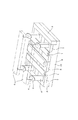
一般的なMRAMの模式図(斜視図)を図12に示す。
シリコン基板等の半導体基体110の素子分離層102により分離された部分に、各メモリセルを選択するための選択用トランジスタを構成する、ドレイン領域108、ソース領域107、並びにゲート電極101が、それぞれ形成されている。
また、ゲート電極101の上方には、図中前後方向に延びるワード線105が設けられている。
ドレイン領域108は、図中左右の選択用トランジスタに共通して形成されており、このドレイン領域108には、配線109が接続されている。
そして、ワード線105と、上方に配置された、図中左右方向に延びるビット線106との間に、磁化の向きが反転する記憶層を有する磁気記憶素子103が配置されている。この磁気記憶素子103は、例えば磁気トンネル接合素子(MTJ素子)により構成される。
さらに、磁気記憶素子103は、水平方向のバイパス線111及び上下方向のコンタクト層104を介して、ソース領域107に電気的に接続されている。
ワード線105及びビット線106にそれぞれ電流を流すことにより、電流磁界を磁気記憶素子103に印加して、これにより磁気記憶素子103の記憶層の磁化の向きを反転させて、情報の記録を行うことができる。
A schematic diagram (perspective view) of a general MRAM is shown in FIG.
A
A
The
A
Further, the
By applying current to each of the
そして、MRAM等の磁気メモリにおいて、記録した情報を安定に保持するためには、情報を記録する磁性層(記憶層)が、一定の保磁力を有していることが必要である。
一方、記録された情報を書き換えるためには、アドレス配線にある程度の電流を流さなければならない。
ところが、MRAMを構成する素子の微細化に従い、アドレス配線も細くなるため、充分な電流が流せなくなってくる。
In order to stably hold recorded information in a magnetic memory such as MRAM, it is necessary that a magnetic layer (storage layer) for recording information has a certain coercive force.
On the other hand, in order to rewrite the recorded information, a certain amount of current must be passed through the address wiring.
However, as the elements constituting the MRAM become finer, the address wiring becomes thinner, so that a sufficient current cannot flow.
そこで、より少ない電流で磁化反転が可能な構成として、スピン注入による磁化反転を利用する構成のメモリが注目されている(例えば、特許文献1、2、4、非特許文献1、2参照)。
スピン注入による磁化反転とは、磁性体の中を通過してスピン偏極した電子を、他の磁性体に注入することにより、他の磁性体において磁化反転を起こさせるものである。
In view of this, attention has been paid to a memory that uses magnetization reversal by spin injection as a configuration that allows magnetization reversal with a smaller current (see, for example,
Magnetization reversal by spin injection is to cause magnetization reversal in another magnetic material by injecting spin-polarized electrons that have passed through the magnetic material into another magnetic material.
例えば、巨大磁気抵抗効果素子(GMR素子)や磁気トンネル接合素子(MTJ素子)に対して、その膜面に垂直な方向に電流を流すことにより、これらの素子の少なくとも一部の磁性層の磁化の向きを反転させることができる。 For example, when a current is passed through a giant magnetoresistive element (GMR element) or a magnetic tunnel junction element (MTJ element) in a direction perpendicular to the film surface, magnetization of at least a part of the magnetic layer of these elements is performed. Can be reversed.
そして、スピン注入による磁化反転は、素子が微細化されても、電流を増やさずに磁化反転を実現することができる利点を有している。 Magnetization reversal by spin injection has an advantage that magnetization reversal can be realized without increasing current even if the element is miniaturized.
上述したスピン注入による磁化反転を利用する構成のメモリ装置の模式図を、図13及び図14に示す。図13は斜視図、図14は断面図である。
シリコン基板等の半導体基体60の素子分離層52により分離された部分に、各メモリセルを選択するための選択用トランジスタを構成する、ドレイン領域58、ソース領域57、並びにゲート電極51が、それぞれ形成されている。このうち、ゲート電極51は、図7中前後方向に延びるワード線を兼ねている。
ドレイン領域58は、図13中左右の選択用トランジスタに共通して形成されており、このドレイン領域58には、配線59が接続されている。
そして、ソース領域57と、上方に配置された、図13中左右方向に延びるビット線56との間に、スピン注入により磁化の向きが反転する記憶層を有する記憶素子53が配置されている。
この記憶素子53は、例えば磁気トンネル接合素子(MTJ素子)により構成される。記憶素子53は2つの磁性層61、62を有する。この2層の磁性層61,62のうち、一方の磁性層を磁化の向きが固定された磁化固定層として、他方の磁性層を磁化の向きが変化する磁化自由層即ち記憶層とする。
また、記憶素子53は、ビット線56と、ソース領域57とに、それぞれ上下のコンタクト層54を介して接続されている。これにより、記憶素子53に電流を流して、スピン注入により記憶層の磁化の向きを反転させることができる。
Schematic diagrams of the memory device configured to use the above-described magnetization reversal by spin injection are shown in FIGS. 13 is a perspective view, and FIG. 14 is a cross-sectional view.
A
The
A
The
The
このようなスピン注入による磁化反転を利用する構成のメモリ装置の場合、図12に示した一般的なMRAMと比較して、デバイス構造を単純化することができ、そのために高密度化が可能になるという特徴も有している。
また、スピン注入による磁化反転を利用することにより、外部磁界により磁化反転を行う一般的なMRAMと比較して、素子の微細化が進んでも、書き込みの電流が増大しないという利点がある。
In the case of a memory device configured to use such magnetization reversal by spin injection, the device structure can be simplified as compared with the general MRAM shown in FIG. It also has the feature of becoming.
Further, by utilizing magnetization reversal by spin injection, there is an advantage that the write current does not increase even when the element is miniaturized as compared with a general MRAM in which magnetization reversal is performed by an external magnetic field.
ところで、MRAMの場合は、記憶素子とは別に書き込み配線(ワード線やビット線)を設けて、書き込み配線に電流を流して発生する電流磁界により、情報の書き込み(記録)を行っている。そのため、書き込み配線に、書き込みに必要となる電流量を充分に流すことができる。
一方、スピン注入による磁化反転を利用する構成のメモリ装置においては、記憶素子に流す電流によりスピン注入を行って、記憶層の磁化の向きを反転させる必要がある。
そして、このように記憶素子に直接電流を流して情報の書き込み(記録)を行うことから、書き込みを行うメモリセルを選択するために、記憶素子を選択トランジスタと接続してメモリセルを構成する。この場合、記憶素子に流れる電流は、選択トランジスタに流すことが可能な電流(選択トランジスタの飽和電流)の大きさに制限される。
このため、選択トランジスタの飽和電流以下の電流で書き込みを行う必要があり、スピン注入の効率を改善して、記憶素子に流す電流を低減する必要がある。
In the case of an MRAM, a write wiring (word line or bit line) is provided separately from a memory element, and information is written (recorded) by a current magnetic field generated by passing a current through the write wiring. Therefore, a sufficient amount of current required for writing can be passed through the write wiring.
On the other hand, in a memory device configured to utilize magnetization reversal by spin injection, it is necessary to reverse the magnetization direction of the storage layer by performing spin injection with a current flowing through the storage element.
Since the current is directly supplied to the memory element and information is written (recorded) as described above, the memory cell is configured by connecting the memory element to a selection transistor in order to select a memory cell to be written. In this case, the current flowing through the memory element is limited to the magnitude of the current that can flow through the selection transistor (the saturation current of the selection transistor).
Therefore, it is necessary to perform writing with a current lower than the saturation current of the selection transistor, and it is necessary to improve the efficiency of spin injection and reduce the current flowing through the memory element.
また、読み出し信号を大きくするためには、大きな磁気抵抗変化率を確保する必要があり、そのためには記憶層の両側に接している中間層をトンネル絶縁層(トンネルバリア層)とした記憶素子の構成にすることが効果的である。
このように中間層としてトンネル絶縁層を用いた場合には、トンネル絶縁層が絶縁破壊することを防ぐために、記憶素子に流す電流量に制限が生じる。この観点からも、スピン注入時の電流を抑制する必要がある。
Also, in order to increase the read signal, it is necessary to secure a large rate of change in magnetoresistance. To that end, a memory element having a tunnel insulating layer (tunnel barrier layer) as an intermediate layer in contact with both sides of the memory layer is required. The configuration is effective.
When the tunnel insulating layer is used as the intermediate layer as described above, the amount of current flowing through the memory element is limited in order to prevent the tunnel insulating layer from being broken down. From this viewpoint, it is necessary to suppress the current during spin injection.
この電流値を下げるためには、この電流値が記憶層の膜厚に比例し、記憶層の飽和磁化の2乗に比例するので、これら(膜厚や飽和磁化)を調節すれば良いことがわかる(例えば、非特許文献3参照)。
そして、例えば特許文献3には、記録材料の磁化量(Ms)を低減すれば、電流値を低減できることが示されている。
In order to reduce the current value, the current value is proportional to the film thickness of the memory layer and proportional to the square of the saturation magnetization of the memory layer. Therefore, it is only necessary to adjust these (film thickness and saturation magnetization). It is understood (for example, refer nonpatent literature 3).
For example,
しかしながら、一方で、電流によって書き込まれた情報を記憶しなければ不揮発性メモリとはなり得ない。つまり、記憶層の熱揺らぎに対する安定性(熱安定性)の確保が必要である。
スピン注入による磁化反転を利用する記憶素子の場合、従来のMRAMと比較して、記憶層の体積が小さくなるので、単純に考えると熱安定性は低下する方向にある。
記憶層の熱安定性が確保されていないと、反転した磁化の向きが、熱により再反転してしまい、書き込みエラーとなってしまう。
そして、スピン注入による磁化反転を利用する記憶素子の大容量化を進めた場合、記録素子の体積は一層小さくなるので、熱安定性の確保は重要な課題となる。
However, on the other hand, if the information written by the current is not stored, it cannot be a nonvolatile memory. That is, it is necessary to ensure the stability (thermal stability) of the storage layer against thermal fluctuation.
In the case of a memory element using magnetization reversal by spin injection, the volume of the memory layer is smaller than that of a conventional MRAM, so that the thermal stability tends to be lowered in a simple way.
If the thermal stability of the storage layer is not ensured, the reversed magnetization direction is reversed again by heat, resulting in a write error.
When the capacity of a storage element that utilizes magnetization reversal by spin injection is increased, the volume of the recording element is further reduced, so ensuring thermal stability becomes an important issue.
そのため、スピン注入による磁化反転を利用する記憶素子において、熱安定性は非常に重要な特性である。 Therefore, thermal stability is a very important characteristic in a memory element using magnetization reversal by spin injection.
従って、スピン注入により記憶層の磁化の向きを反転させる構成の記憶素子がメモリとして存在し得るためには、スピン注入による磁化反転に必要な電流をトランジスタの飽和電流以下に減らし、また、書き込まれた情報をしっかり保持する熱安定性を確保する必要がある。 Therefore, in order for a memory element configured to reverse the magnetization direction of the memory layer by spin injection to exist as a memory, the current required for magnetization reversal by spin injection is reduced below the saturation current of the transistor and written. It is necessary to ensure the thermal stability to hold the information firmly.
以上のように、スピン注入による磁化反転に必要な電流を低減するには、記憶層の飽和磁化量Msを低減することや、記憶層を薄くすることが考えられる。例えば、上述の特許文献3のように、記憶層の材料に、飽和磁化量Msの低い材料を使用することが有効である。
As described above, in order to reduce the current required for magnetization reversal by spin injection, it is conceivable to reduce the saturation magnetization amount Ms of the storage layer or to make the storage layer thinner. For example, as in
しかしながら、このように、単純に飽和磁化量Msの低い材料を用いた場合、情報をしっかりと保持する熱安定性を確保することができない。
ST−MRAMにおいては、書き込み電流を増大させることなく、熱安定性を改善することができる記憶素子の実現が望まれるものである。
However, as described above, when a material having a low saturation magnetization Ms is simply used, it is not possible to ensure thermal stability that holds information firmly.
In the ST-MRAM, it is desired to realize a memory element that can improve the thermal stability without increasing the write current.
ここで、ST−MRAMに用いる強磁性体として、さまざまな材料が検討されているが、一般に面内磁気異方性を有するものよりも垂直磁気異方性を有するものの方が低電力化、大容量化に適しているとされている。これは垂直磁化の方がスピントルク磁化反転の際に超えるべきエネルギバリアが低く、また垂直磁化膜の有する高い磁気異方性が大容量化により微細化した記憶担体の熱安定性を保持するのに有利であるためである。 Here, various materials have been studied as a ferromagnetic material used in the ST-MRAM. In general, a material having perpendicular magnetic anisotropy has a lower power and a larger power than those having in-plane magnetic anisotropy. It is said that it is suitable for capacity increase. This is because the perpendicular magnetization has a lower energy barrier that must be exceeded during spin torque magnetization reversal, and the high magnetic anisotropy of the perpendicular magnetization film retains the thermal stability of the memory carrier miniaturized by increasing the capacity. It is because it is advantageous to.
垂直異方性を有する磁性材料としては、CoとFeとを含有する合金を採用するものが知られているが、このような磁性材料を用いた場合には、その組成としてFeを含むことにより、プロセスや熱処理において、酸化、つまりは腐食による抵抗の上昇が促進されてしまう虞がある。
特に、素子直径を100nm以下に微細化することが要求される高密度記録素子(ひいては大容量メモリ)では、外周部からの磁性層への侵食による抵抗上昇が無視できなくなるという問題がある。
As a magnetic material having perpendicular anisotropy, one using an alloy containing Co and Fe is known. However, when such a magnetic material is used, the composition contains Fe. In the process and heat treatment, there is a possibility that the increase in resistance due to oxidation, that is, corrosion, is promoted.
In particular, a high-density recording element (and consequently a large capacity memory) that is required to be miniaturized to an element diameter of 100 nm or less has a problem that a resistance increase due to erosion to the magnetic layer from the outer peripheral portion cannot be ignored.
本発明は以上の問題点に鑑み為されたものであり、ST−MRAMにおいて、書き込み電流の低減と熱安定性との両立を図ると共に、記憶層の微細加工時の抵抗上昇を防止し、低消費電力な記憶素子を提供することをその課題とする。 The present invention has been made in view of the above problems. In the ST-MRAM, while reducing both the write current and the thermal stability, the resistance increase at the time of microfabrication of the memory layer is prevented, and the low It is an object to provide a power consumption memory element.
本発明の記憶素子は、膜面に垂直な磁化を有し、情報に対応して磁化の向きが変化される記憶層と、上記記憶層に記憶された情報の基準となる膜面に垂直な磁化を有する磁化固定層と、上記記憶層と上記磁化固定層の間に設けられる非磁性体による絶縁層とを有する。
そして、上記記憶層、上記絶縁層、上記磁化固定層を有する層構造の積層方向にスピン偏極した電子を注入することにより、上記記憶層の磁化の向きが変化して、上記記憶層に対して情報の記録が行われるとともに、上記記憶層が受ける、実効的な反磁界の大きさが、上記記憶層の飽和磁化量よりも小さくなるように構成される。
さらに、上記記憶層を構成する強磁性層材料が、Co−Fe−Bを母材とし且つ当該母材に耐食性元素が添加されて成るものである。
The memory element of the present invention has a magnetization perpendicular to the film surface, the magnetization direction of which changes in accordance with information, and a film perpendicular to the film surface serving as a reference for information stored in the memory layer. A magnetization fixed layer having magnetization; and an insulating layer made of a nonmagnetic material provided between the storage layer and the magnetization fixed layer.
Then, by injecting spin-polarized electrons in the stacking direction of the layer structure having the memory layer, the insulating layer, and the magnetization fixed layer, the magnetization direction of the memory layer changes, and the memory layer Information is recorded, and the effective demagnetizing field received by the storage layer is configured to be smaller than the saturation magnetization of the storage layer.
Further, the ferromagnetic layer material constituting the memory layer is formed by using Co—Fe—B as a base material and adding a corrosion-resistant element to the base material.
また、本発明のメモリ装置は、情報を磁性体の磁化状態により保持する記憶素子と、互いに交差する2種類の配線とを備え、記憶素子は上記本発明の記憶素子の構成であり、2種類の配線の間に記憶素子が配置され、これら2種類の配線を通じて、記憶素子に積層方向の電流が流れ、スピン偏極した電子が注入されるものである。 The memory device of the present invention includes a memory element that holds information according to the magnetization state of the magnetic material, and two types of wirings that intersect each other, and the memory element has the configuration of the memory element of the present invention. A memory element is arranged between the two wirings, and a current in the stacking direction flows through the memory element through these two types of wiring, and spin-polarized electrons are injected.
上記による本発明の記憶素子の構成によれば、情報を磁性体の磁化状態により保持する記憶層を有し、この記憶層に対して中間層を介して磁化固定層が設けられ、中間層が絶縁体から成り、積層方向にスピン偏極した電子を注入することにより、記憶層の磁化の向きが変化して、記憶層に対して情報の記録が行われるので、積層方向に電流を流してスピン偏極した電子を注入することによって情報の記録を行うことができる。
そして、記憶層が受ける、実効的な反磁界の大きさが、記憶層の飽和磁化量よりも小さいことにより、記憶層が受ける反磁界が低くなっており、記憶層の磁化の向きを反転させるために必要となる、書き込み電流量を低減することができる。
一方、記憶層の飽和磁化量を低減しなくても書き込み電流量を低減することができるため、記憶層の飽和磁化量を充分な量として、記憶層の熱安定性を充分に確保することが可能になる。
さらに、本発明の記憶素子は、記憶層及び磁化固定層は膜面に垂直な磁化を有する。面内磁気異方性を有するものよりも垂直磁気異方性を有するものの方が低電力化、大容量化に好適である。理由は垂直磁化の方がスピントルク磁化反転の際に超えるべきエネルギバリアが低く、また垂直磁化膜の有する高い磁気異方性によって記憶層の情報保持の熱安定性が有利になるためである。
According to the configuration of the memory element of the present invention as described above, it has a memory layer that holds information according to the magnetization state of the magnetic material, and a magnetization pinned layer is provided via this intermediate layer with respect to this memory layer. By injecting electrons that are made of an insulator and spin-polarized in the stacking direction, the magnetization direction of the storage layer changes and information is recorded on the storage layer. Information can be recorded by injecting spin-polarized electrons.
Since the effective demagnetizing field received by the storage layer is smaller than the saturation magnetization of the storage layer, the demagnetizing field received by the storage layer is low, and the magnetization direction of the storage layer is reversed. Therefore, it is possible to reduce the amount of write current required.
On the other hand, since the amount of write current can be reduced without reducing the saturation magnetization amount of the storage layer, it is possible to sufficiently secure the thermal stability of the storage layer by making the saturation magnetization amount of the storage layer sufficient. It becomes possible.
Furthermore, in the memory element of the present invention, the memory layer and the magnetization fixed layer have magnetization perpendicular to the film surface. Those having perpendicular magnetic anisotropy are more suitable for reducing power and increasing capacity than those having in-plane magnetic anisotropy. The reason is that the perpendicular magnetization has a lower energy barrier to be exceeded when the spin torque magnetization is reversed, and the high magnetic anisotropy of the perpendicular magnetization film makes the thermal stability of information storage in the storage layer more advantageous.
また、本発明の記憶素子は、記憶層を構成する強磁性層材料が、Co−Fe−Bを母材とし且つ当該母材に耐食性元素が添加されて成る。このことで、記憶層の微細加工時の抵抗上昇を防止し、低消費電力な記憶素子を提供することができる。 In the memory element of the present invention, the ferromagnetic layer material constituting the memory layer is made by using Co—Fe—B as a base material and adding a corrosion-resistant element to the base material. As a result, it is possible to provide a memory element that can prevent an increase in resistance at the time of microfabrication of the memory layer and has low power consumption.
また上述の本発明のメモリ装置の構成によれば、2種類の配線の間に記憶素子が配置され、これら2種類の配線を通じて記憶素子に積層方向の電流が流れ、スピン偏極した電子が注入されるものであることにより、2種類の配線を通じて記憶素子の積層方向に電流を流してスピン注入による情報の記録を行うことができる。
また、記憶層の飽和磁化量を低減しなくても、記憶素子の書き込み電流量を低減することが可能になるため、記憶素子に記録された情報を安定して保持すると共に、メモリ装置の消費電力を低減することが可能になる。
また、上述のようにこの場合の記憶素子は、記憶層を構成する強磁性層材料の母材に耐食性元素が添加されていることで、記憶層の微細加工時の抵抗上昇が防止されるものとなり、この点でも低消費電力なメモリ装置の実現が図られる。また記憶層を構成する強磁性層材料の母材に耐食性元素が添加されることによっては、熱安定性の向上も図られる。
Further, according to the configuration of the memory device of the present invention described above, the memory element is arranged between the two types of wirings, current in the stacking direction flows through the memory elements through these two types of wirings, and spin-polarized electrons are injected. Thus, information can be recorded by spin injection by flowing current in the stacking direction of the memory element through two types of wiring.
Further, since it becomes possible to reduce the amount of write current of the storage element without reducing the saturation magnetization amount of the storage layer, it is possible to stably hold the information recorded in the storage element and to consume the memory device. It becomes possible to reduce electric power.
In addition, as described above, the memory element in this case has an anti-corrosion element added to the base material of the ferromagnetic layer material constituting the memory layer, thereby preventing an increase in resistance when the memory layer is finely processed. In this respect, a memory device with low power consumption can be realized. Further, by adding a corrosion-resistant element to the base material of the ferromagnetic layer material constituting the memory layer, the thermal stability can be improved.
本発明によれば、記憶層の飽和磁化量を低減しなくても、記憶素子の書き込み電流量を低減することが可能になるため、情報保持能力である熱安定性を充分に確保して、特性バランスに優れた記憶素子を構成することができる。これにより、動作エラーをなくして、記憶素子の動作マージンを充分に得ることができる。
従って、安定して動作する、信頼性の高いメモリ装置を実現することができる。
また、書き込み電流を低減して、記憶素子に書き込みを行う際の消費電力を低減することが可能になる。つまりこの点において、メモリ装置全体の消費電力を低減することが可能になる。
また本発明によれば、記憶層を構成する強磁性層材料の母材に耐食性元素が添加されていることで、記憶層の微細加工時の抵抗上昇が防止され、この点でも低消費電力なメモリ装置の実現化が図られる。
また、記憶層を構成する強磁性層材料の母材に耐食性元素が添加されることで、熱安定性の向上にも寄与する。
According to the present invention, it is possible to reduce the write current amount of the storage element without reducing the saturation magnetization amount of the storage layer. A memory element having excellent characteristic balance can be configured. Thereby, an operation error can be eliminated and a sufficient operation margin of the memory element can be obtained.
Therefore, a highly reliable memory device that operates stably can be realized.
In addition, the write current can be reduced, so that power consumption when writing to the memory element can be reduced. That is, in this respect, the power consumption of the entire memory device can be reduced.
Further, according to the present invention, the addition of a corrosion-resistant element to the base material of the ferromagnetic layer material constituting the memory layer prevents an increase in resistance during microfabrication of the memory layer, and in this respect also low power consumption. Realization of a memory device is achieved.
In addition, the addition of a corrosion-resistant element to the base material of the ferromagnetic layer material constituting the memory layer contributes to the improvement of thermal stability.
以下、本発明の実施の形態を次の順序で説明する。
<1.先行例としての記憶素子>
[1-1.先行例の記憶素子の概要]
[1-2.先行例1の構成]
[1-3.先行例1に関する実験]
[1-4.先行例2の構成]
[1-5.先行例2に関する実験]
<2.実施の形態の記憶素子>
[2-1.先行例の課題について]
[2-2.実施の形態の記憶素子の構成]
[2-3.実施の形態の記憶素子についての実験]
<3.変形例>
Hereinafter, embodiments of the present invention will be described in the following order.
<1. Memory element as a prior example>
[1-1. Overview of memory element of previous example]
[1-2. Configuration of Prior Example 1]
[1-3. Experiment on Prior Example 1]
[1-4. Configuration of Prior Example 2]
[1-5. Experiment on Prior Example 2]
<2. Memory Element of Embodiment>
[2-1. About the problem of the previous example]
[2-2. Configuration of Memory Element of Embodiment]
[2-3. Experiments on storage element of embodiment]
<3. Modification>
<1.先行例としての記憶素子>
[1-1.先行例の記憶素子の概要]
まず、本発明の記憶素子を見出すにあたりその基とした、先行例としての記憶素子の概要について説明する。
先行例(及び後述する実施の形態)としての記憶素子は、前述したスピン注入により、記憶素子の記憶層の磁化の向きを反転させて、情報の記録を行うものである。
記憶層は、強磁性層等の磁性体により構成され、情報を磁性体の磁化状態(磁化の向き)により保持するものである。
<1. Memory element as a prior example>
[1-1. Overview of memory element of previous example]
First, an outline of a memory element as a prior example based on which the memory element of the present invention is found will be described.
A memory element as a preceding example (and an embodiment described later) records information by reversing the magnetization direction of the memory layer of the memory element by the above-described spin injection.
The memory layer is made of a magnetic material such as a ferromagnetic layer, and holds information by the magnetization state (magnetization direction) of the magnetic material.
詳しくは後述するが、記憶素子は、例えば図2に一例を示す層構造とされ、少なくとも2つの磁性層としての記憶層17、磁化固定層15を備え、またその2つの磁性層の間の中間層としての絶縁層16(トンネル絶縁層)を備える。
記憶層17は、膜面に垂直な磁化を有し、情報に対応して磁化の向きが変化される。
磁化固定層15は、記憶層17に記憶された情報の基準となる膜面に垂直な磁化を有する。
絶縁層16は、非磁性体であって、記憶層17と磁化固定層15の間に設けられる。
そして記憶層17、絶縁層16、磁化固定層15を有する層構造の積層方向にスピン偏極した電子を注入することにより、記憶層17の磁化の向きが変化して、記憶層17に対して情報の記録が行われる。
As will be described in detail later, the storage element has a layer structure as shown in FIG. 2, for example. The storage element includes at least two
The
The magnetization fixed
The insulating
Then, by injecting spin-polarized electrons in the stacking direction of the layer structure having the
スピン注入により磁性層(記憶層17)の磁化の向きを反転させる基本的な動作は、巨大磁気抵抗効果素子(GMR素子)もしくはトンネル磁気抵抗効果素子(MTJ素子)から成る記憶素子に対して、その膜面に垂直な方向に、ある閾値以上の電流を流すものである。このとき、電流の極性(向き)は、反転させる磁化の向きに依存する。
この閾値よりも絶対値が小さい電流を流した場合には、磁化反転を生じない。
The basic operation of reversing the direction of magnetization of the magnetic layer (memory layer 17) by spin injection is performed on a memory element composed of a giant magnetoresistive element (GMR element) or a tunnel magnetoresistive element (MTJ element). A current exceeding a certain threshold is passed in a direction perpendicular to the film surface. At this time, the polarity (direction) of the current depends on the direction of magnetization to be reversed.
When a current having an absolute value smaller than this threshold is passed, magnetization reversal does not occur.
スピン注入によって、磁性層の磁化の向きを反転させるときに、必要となる電流の閾値Icは一般的には、
Ic=A・α・Ms・V・Hd/2η
により表される。
ここで、A:定数、α:スピン制動定数、η:スピン注入効率、Ms:飽和磁化量、V:記憶層の体積、Hd:実効的な反磁界である。
この式で表されるように、電流の閾値は、磁性層の体積V、磁性層の飽和磁化Ms、スピン注入効率η、スピン制動定数αを制御することにより、任意に設定することが可能である。
When the magnetization direction of the magnetic layer is reversed by spin injection, the required current threshold Ic is generally
Ic = A · α · Ms · V · Hd / 2η
It is represented by
Here, A: constant, α: spin braking constant, η: spin injection efficiency, Ms: saturation magnetization, V: volume of storage layer, Hd: effective demagnetizing field.
As represented by this equation, the threshold value of the current can be arbitrarily set by controlling the volume V of the magnetic layer, the saturation magnetization Ms of the magnetic layer, the spin injection efficiency η, and the spin braking constant α. is there.
なお厳密には、スピントルク磁化反転によって、磁性層の磁化の向きを反転させるときに、必要となる電流の閾値Icは、磁性層の磁化容易軸が面内方向であるか、垂直方向であるかによって異なる。
先行例や実施の形態の記憶素子は垂直磁化型であるが、従前の面内磁化型の記憶素子の場合における磁性層の磁化の向きを反転させる反転電流をIc_paraとすると、
同方向から逆方向(なお、同方向、逆方向とは、磁化固定層の磁化方向を基準としてみた記憶層の磁化方向)に反転させる場合、
Ic_para=(A・α・Ms・V/g(0)/P)(Hk+2πMs)
となり、逆方向から同方向に反転させる場合、
Ic_para=−(A・α・Ms・V/g(π)/P)(Hk+2πMs)
となる。
Strictly speaking, when the magnetization direction of the magnetic layer is reversed by spin torque magnetization reversal, the required current threshold Ic is the in-plane direction or the perpendicular direction of the magnetization easy axis of the magnetic layer. It depends on what.
The storage elements of the preceding examples and embodiments are of the perpendicular magnetization type, but if the reversal current that reverses the magnetization direction of the magnetic layer in the case of the conventional in-plane magnetization type storage element is Ic_para,
When reversing from the same direction to the reverse direction (note that the same direction and the reverse direction are the magnetization directions of the storage layer with reference to the magnetization direction of the magnetization fixed layer)
Ic_para = (A · α · Ms · V / g (0) / P) (Hk + 2πMs)
And when reversing from the opposite direction to the same direction,
Ic_para = − (A · α · Ms · V / g (π) / P) (Hk + 2πMs)
It becomes.
一方、本例のような垂直磁化型の記憶素子の反転電流をIc_perpとすると、同方向から逆方向に反転させる場合、
Ic_perp=(A・α・Ms・V/g(0)/P)(Hk−4πMs)
となり、逆方向から同方向に反転させる場合、
Ic_perp=−(A・α・Ms・V/g(π)/P)(Hk−4πMs)
となる。
On the other hand, when the reversal current of the perpendicular magnetization type storage element as in this example is Ic_perp, when reversing from the same direction to the reverse direction,
Ic_perp = (A · α · Ms · V / g (0) / P) (Hk−4πMs)
And when reversing from the opposite direction to the same direction,
Ic_perp = − (A · α · Ms · V / g (π) / P) (Hk−4πMs)
It becomes.
ただし、Aは定数、αはダンピング定数、Msは飽和磁化、Vは素子体積、Pはスピン分極率、g(0)、g(π)はそれぞれ同方向時、逆方向時にスピントルクが相手の磁性層に伝達される効率に対応する係数、Hkは磁気異方性である(非特許文献4参照)。 Where A is a constant, α is a damping constant, Ms is saturation magnetization, V is element volume, P is spin polarizability, g (0) and g (π) are in the same direction and spin torque in the opposite direction. A coefficient Hk corresponding to the efficiency transmitted to the magnetic layer is magnetic anisotropy (see Non-Patent Document 4).
上記各式において、垂直磁化型の場合の(Hk−4πMs)と面内磁化型の場合の(Hk+2πMs)とを比較すると、垂直磁化型が低記録電流化により適していることが理解できる。 In each of the above formulas, comparing (Hk−4πMs) in the perpendicular magnetization type and (Hk + 2πMs) in the in-plane magnetization type, it can be understood that the perpendicular magnetization type is more suitable for reducing the recording current.
本例の記憶素子は、トンネル磁気抵抗効果による抵抗の差で情報の読み出しを行う。つまり、トンネル磁気抵抗効果が大きい場合に出力も大きくなる。トンネル磁気抵抗効果TMRは、スピン分極率:Pを用いて式(1)により表される。 The memory element of this example reads information by the difference in resistance due to the tunnel magnetoresistance effect. That is, when the tunnel magnetoresistance effect is large, the output is also large. The tunnel magnetoresistive effect TMR is expressed by the formula (1) using the spin polarizability: P.

ここで、P1は固定層のスピン分極率、P2は記録層のスピン分極率である。式(1)において、スピン分極率が大きいときに、TMRが大きくなることが理解できる。
そして、反転電流の式との比較により、低電流化と高出力化(=高TMR化)が両立する関係であることも分かる。
Here, P1 is the spin polarizability of the fixed layer, and P2 is the spin polarizability of the recording layer. In equation (1), it can be understood that TMR increases when the spin polarizability is large.
It can also be seen from the comparison with the reversal current equation that both a low current and a high output (= high TMR) are compatible.
先行例及び実施の形態では、磁化状態により情報を保持することができる磁性層(記憶層17)と、磁化の向きが固定された磁化固定層15とを有する記憶素子を構成する。
メモリとして存在し得るためには、書き込まれた情報を保持することができなければならない。情報を保持する能力の指標として、熱安定性の指標Δ(=KV/kBT)の値で判断される。このΔは、下記式(2)により表される。
In the preceding example and the embodiment, a storage element including a magnetic layer (storage layer 17) capable of retaining information according to a magnetization state and a magnetization fixed
In order to be able to exist as a memory, it must be able to hold the written information. As an index of the ability to hold information, it is determined by the value of the thermal stability index Δ (= KV / k B T). This Δ is represented by the following formula (2).
![]()
ここで、Hk:実効的な異方性磁界、kB:ボルツマン定数、T:温度、Ms:飽和磁化量、V:記憶層の体積である。
![]()
Here, Hk: effective anisotropic magnetic field, k B : Boltzmann constant, T: temperature, Ms: saturation magnetization, and V: volume of the storage layer.
実効的な異方性磁界Hkには、形状磁気異方性、誘導磁気異方性、結晶磁気異方性等の影響が取り込まれており、単磁区のコヒーレントローテンションモデルを仮定した場合、保磁力と同等である。 The effective anisotropy magnetic field Hk incorporates effects such as shape magnetic anisotropy, induced magnetic anisotropy, and magnetocrystalline anisotropy. When a single domain coherent rotation model is assumed, It is equivalent to magnetic force.
熱安定性の指標Δと電流の閾値Icとは、トレードオフの関係になることが多い。そのため、メモリ特性を維持するには、これらの両立が課題となることが多い。 The thermal stability index Δ and the current threshold value Ic often have a trade-off relationship. Therefore, in order to maintain the memory characteristics, it is often a problem to achieve both.
記憶層17の磁化状態を変化させる電流の閾値は、実際には、例えば記憶層17の厚さが2nmであり、平面パターンが100nm×150nmの略楕円形のTMR素子において、+側の閾値+Ic=+0.5mAであり、−側の閾値−Ic=−0.3mAであり、その際の電流密度は約3.5×10⁶A/cm2である。これらは、上記のIcの式にほぼ一致する。
The threshold value of the current for changing the magnetization state of the
これに対して、電流磁場により磁化反転を行う通常のMRAMでは、書き込み電流が数mA以上必要となる。
従って、スピン注入によって磁化反転を行う場合には、上述のように書き込み電流の閾値が充分に小さくなるため、集積回路の消費電力を低減させるために有効であることが分かる。
また、通常のMRAMで必要とされる、電流磁界発生用の配線(図12の配線105)が不要となるため、集積度においても通常のMRAMに比較して有利である。
On the other hand, in a normal MRAM that performs magnetization reversal by a current magnetic field, a write current of several mA or more is required.
Therefore, it can be seen that when the magnetization reversal is performed by spin injection, the threshold value of the write current becomes sufficiently small as described above, which is effective in reducing the power consumption of the integrated circuit.
In addition, the current magnetic field generating wiring (
そして、スピン注入により磁化反転を行う場合には、記憶素子に直接電流を流して情報の書き込み(記録)を行うことから、書き込みを行うメモリセルを選択するために、記憶素子を選択トランジスタと接続してメモリセルを構成する。
この場合、記憶素子に流れる電流は、選択トランジスタで流すことが可能な電流(選択トランジスタの飽和電流)の大きさによって制限される。
When magnetization reversal is performed by spin injection, information is written (recorded) by directly passing a current through the memory element. Therefore, the memory element is connected to a selection transistor in order to select a memory cell to be written. Thus, a memory cell is configured.
In this case, the current flowing through the memory element is limited by the magnitude of the current that can be passed through the selection transistor (the saturation current of the selection transistor).
選択トランジスタの飽和電流よりも、スピン注入による磁化反転の電流の閾値Icを小さくするためには、上記Icの式より、記憶層17の飽和磁化量Msを減らせば良いことがわかる。
しかし、単純に飽和磁化量Msを減らした場合(例えば、特許文献3)には、記憶層17の熱安定性が著しく損なわれ、メモリとしての機能を果せなくなる。
メモリを構成するためには、熱安定性の指標Δがある程度以上の大きさである必要がある。
It can be seen from the above formula Ic that the saturation magnetization amount Ms of the
However, when the saturation magnetization amount Ms is simply reduced (for example, Patent Document 3), the thermal stability of the
In order to configure the memory, it is necessary that the thermal stability index Δ is larger than a certain level.
そこで、本願の発明者等が種々の検討を行った結果、記憶層17を構成する強磁性層として、例えばCo−Fe−Bの組成を選定することにより、記憶層17が受ける実効的な反磁界(Meffective)の大きさが、記憶層17の飽和磁化量Msよりも小さくなることを見出した。
上述の強磁性材料を用いることにより、記憶層17が受ける実効的な反磁界の大きさが、記憶層17の飽和磁化量Msよりも小さい構成となる。
これにより、記憶層17が受ける反磁界を小さくすることができるので、式(2)により表される熱安定性Δを損ねることなく、上記Icの式により表される電流の閾値Icを低減する効果が得られる。
さらに、発明者らは、上記の選定されたCo−Fe−B組成の内、限られた組成範囲において、Co−Fe−Bが膜面垂直方向に磁化し、それにより、Gbitクラスの容量を実現可能な極微小記録素子においても十分な熱安定性が確保可能であることを見出した。
従って、Gbitクラスのスピン注入型磁化反転メモリにおいて熱安定性を保った状態で、低電流で情報の書き込みができる、という安定したメモリの形成を可能にする。
Therefore, as a result of various studies by the inventors of the present application, an effective reaction that the
By using the above-described ferromagnetic material, the effective demagnetizing field received by the
As a result, the demagnetizing field received by the
Furthermore, the inventors have magnetized Co—Fe—B in the direction perpendicular to the film surface in the limited composition range of the selected Co—Fe—B composition, thereby increasing the capacity of the Gbit class. It has been found that sufficient thermal stability can be secured even in a feasible micro-recording element.
Therefore, it is possible to form a stable memory in which information can be written with a low current while maintaining thermal stability in a Gbit class spin-injection type magnetization reversal memory.
先行例及び実施の形態では、記憶層17が受ける実効的な反磁界の大きさが、記憶層17の飽和磁化量Msよりも小さい構成、即ち、記憶層17の飽和磁化量Msに対する実効的な反磁界の大きさの比の値を1より小さくする。
In the preceding example and the embodiment, the effective demagnetizing field received by the
さらに、選択トランジスタの飽和電流値を考慮して、記憶層17と磁化固定層15との間の非磁性の中間層として、絶縁体から成るトンネル絶縁層(絶縁層16)を用いて磁気トンネル接合(MTJ)素子を構成する。
トンネル絶縁層を用いて磁気トンネル接合(MTJ)素子を構成することにより、非磁性導電層を用いて巨大磁気抵抗効果(GMR)素子を構成した場合と比較して、磁気抵抗変化率(MR比)を大きくすることができ、読み出し信号強度を大きくすることができるためである。
Further, in consideration of the saturation current value of the selection transistor, a magnetic tunnel junction is formed by using a tunnel insulating layer (insulating layer 16) made of an insulator as a nonmagnetic intermediate layer between the
By constructing a magnetic tunnel junction (MTJ) element using a tunnel insulating layer, a magnetoresistance change rate (MR ratio) is compared with a case where a giant magnetoresistive effect (GMR) element is constructed using a nonmagnetic conductive layer. This is because the read signal intensity can be increased.
そして、特に、このトンネル絶縁層16の材料として、酸化マグネシウム(MgO)を用いることにより、これまで一般的に用いられてきた酸化アルミニウムを用いた場合よりも、磁気抵抗変化率(MR比)を大きくすることができる。
また、一般に、スピン注入効率はMR比に依存し、MR比が大きいほど、スピン注入効率が向上し、磁化反転電流密度を低減することができる。
従って、中間層であるトンネル絶縁層16の材料として酸化マグネシウムを用い、同時に上記の記憶層17を用いることにより、スピン注入による書き込み閾値電流を低減することができ、少ない電流で情報の書き込み(記録)を行うことができる。また、読み出し信号強度を大きくすることができる。
これにより、MR比(TMR比)を確保して、スピン注入による書き込み閾値電流を低減することができ、少ない電流で情報の書き込み(記録)を行うことができる。また、読み出し信号強度を大きくすることができる。
In particular, by using magnesium oxide (MgO) as the material of the
In general, the spin injection efficiency depends on the MR ratio, and the larger the MR ratio, the higher the spin injection efficiency and the lower the magnetization reversal current density.
Therefore, by using magnesium oxide as the material of the
As a result, the MR ratio (TMR ratio) can be ensured, the write threshold current by spin injection can be reduced, and information can be written (recorded) with a small current. In addition, the read signal intensity can be increased.
このようにトンネル絶縁層16を酸化マグネシウム(MgO)膜により形成する場合には、MgO膜が結晶化していて、(001)方向に結晶配向性を維持していることがより望ましい。
Thus, when the
なお、記憶層17と磁化固定層15との間の中間層(トンネル絶縁層16)は、酸化マグネシウムから成る構成とする他にも、例えば酸化アルミニウム、窒化アルミニウム、SiO2、Bi2O3、MgF2、CaF、SrTiO2、AlLaO3、Al−N−O等の各種の絶縁体、誘電体、半導体を用いて構成することもできる。
In addition, the intermediate layer (tunnel insulating layer 16) between the
トンネル絶縁層16の面積抵抗値は、スピン注入により記憶層17の磁化の向きを反転させるために必要な電流密度を得る観点から、数十Ωμm2程度以下に制御する必要がある。
そして、MgO膜から成るトンネル絶縁層16では、面積抵抗値を上述の範囲とするために、MgO膜の膜厚を1.5nm以下に設定する必要がある。
The area resistance value of the
In the
また、記憶層17の磁化の向きを、小さい電流で容易に反転できるように、記憶素子を小さくすることが望ましい。
従って、好ましくは、記憶素子の面積を0.01μm2以下とする。
In addition, it is desirable to make the memory element small so that the magnetization direction of the
Therefore, preferably, the area of the memory element is 0.01 μm 2 or less.
なお、記憶層17は、組成の異なる他の強磁性層を直接積層させることも可能である。また、強磁性層と軟磁性層とを積層させたり、複数層の強磁性層を軟磁性層や非磁性層を介して積層させたりすることも可能である。このように積層させた場合でも、先行例としての効果が得られる。
特に複数層の強磁性層を非磁性層に介して積層させた構成としたときには、強磁性層の層間の相互作用の強さを調整することが可能になるため、記憶素子の寸法がサブミクロン以下になっても、磁化反転電流が大きくならないように抑制することが可能になるという効果が得られる。この場合の非磁性層の材料としては、Ru,Os,Re,Ir,Au,Ag,Cu,Al,Bi,Si,B,C,Cr,Ta,Pd,Pt,Zr,Hf,W,Mo,Nbまたはそれらの合金を用いることができる。
The
In particular, when a configuration in which a plurality of ferromagnetic layers are laminated via a nonmagnetic layer, the strength of the interaction between the ferromagnetic layers can be adjusted. Even if it becomes below, the effect that it becomes possible to suppress so that a magnetization reversal current may not become large is acquired. The material of the nonmagnetic layer in this case is Ru, Os, Re, Ir, Au, Ag, Cu, Al, Bi, Si, B, C, Cr, Ta, Pd, Pt, Zr, Hf, W, Mo. , Nb or their alloys can be used.
磁化固定層15及び記憶層17は、一方向の異方性を有していることが望ましい。
また、磁化固定層15及び記憶層17のそれぞれの膜厚は、0.5nm〜30nmであることが好ましい。
It is desirable that the magnetization fixed
The film thicknesses of the magnetization fixed
記憶素子のその他の構成は、スピン注入により情報を記録する記憶素子の従来公知の構成と同様とすることができる。 The other configuration of the storage element can be the same as a conventionally known configuration of the storage element that records information by spin injection.
磁化固定層15は、強磁性層のみにより、或いは反強磁性層と強磁性層の反強磁性結合を利用することにより、その磁化の向きが固定された構成とすることが出来る。
また、磁化固定層15は、単層の強磁性層から成る構成、或いは複数層の強磁性層を非磁性層を介して積層した積層フェリピン構造とすることが出来る。
積層フェリピン構造の磁化固定層15を構成する強磁性層の材料としては、Co,CoFe,CoFeB等を用いることができる。また、非磁性層の材料としては、Ru,Re,Ir,Os等を用いることができる。
The magnetization pinned
In addition, the magnetization fixed
Co, CoFe, CoFeB, or the like can be used as the material of the ferromagnetic layer constituting the magnetization fixed
反強磁性層の材料としては、FeMn合金、PtMn合金、PtCrMn合金、NiMn合金、IrMn合金、NiO、Fe2O3等の磁性体を挙げることができる。
また、これらの磁性体に、Ag,Cu,Au,Al,Si,Bi,Ta,B,C,O,N,Pd,Pt,Zr,Hf,Ir,W,Mo,Nb等の非磁性元素を添加して、磁気特性を調整したり、その他の結晶構造や結晶性や物質の安定性等の各種物性を調整したりすることができる。
Examples of the material of the antiferromagnetic layer include magnetic materials such as FeMn alloy, PtMn alloy, PtCrMn alloy, NiMn alloy, IrMn alloy, NiO, and Fe 2 O 3 .
In addition, nonmagnetic elements such as Ag, Cu, Au, Al, Si, Bi, Ta, B, C, O, N, Pd, Pt, Zr, Hf, Ir, W, Mo, and Nb are included in these magnetic materials. Can be added to adjust the magnetic properties and other physical properties such as crystal structure, crystallinity and material stability.
また、記憶素子の膜構成は、記憶層17が磁化固定層15の下側に配置される構成でも、下側に配置される構成でも全く問題はない。さらには、磁化固定層15が記憶層17の上下に存在する、いわゆるデュアル構造でも全く問題ない。
In addition, the film configuration of the storage element has no problem whether the
なお、記憶素子の記憶層17に記録された情報を読み出す方法としては、記憶素子の記憶層17に薄い絶縁膜を介して、情報の基準となる磁性層を設けて、絶縁層16を介して流れる強磁性トンネル電流によって読み出してもよいし、磁気抵抗効果により読み出してもよい。
As a method for reading information recorded in the
[1-2.先行例1の構成]
本発明の先行例については、先行例1と先行例2の2例がある。
先ずは先行例1について、具体的構成を説明する。
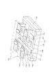
先行例1としてのメモリ装置の概略構成図(斜視図)を図1に示す。
このメモリ装置は、互いに直交する2種類のアドレス配線(例えばワード線とビット線)の交点付近に、磁化状態で情報を保持することができる記憶素子3が配置されて成る。
即ち、シリコン基板等の半導体基体10の素子分離層2により分離された部分に、各メモリセルを選択するための選択用トランジスタを構成する、ドレイン領域8、ソース領域7、並びにゲート電極1が、それぞれ形成されている。このうち、ゲート電極1は、図中前後方向に延びる一方のアドレス配線(例えばワード線)を兼ねている。
ドレイン領域8は、図中左右の選択用トランジスタに共通して形成されており、このドレイン領域8には、配線9が接続されている。
[1-2. Configuration of Prior Example 1]
There are two prior examples of the present invention, the first example and the second example.
First, a specific configuration of the first example will be described.
FIG. 1 shows a schematic configuration diagram (perspective view) of the memory device as the first example.
In this memory device, a
That is, the
The
そして、ソース領域7と、上方に配置された、図中左右方向に延びる他方のアドレス配線(例えばビット線)6との間に、記憶素子3が配置されている。この記憶素子3は、スピン注入により磁化の向きが反転する強磁性層から成る記憶層を有する。
また、この記憶素子3は、2種類のアドレス配線1,6の交点付近に配置されている。
この記憶素子3は、ビット線6と、ソース領域7とに、それぞれ上下のコンタクト層4を介して接続されている。
これにより、2種類のアドレス配線1,6を通じて、記憶素子3に上下方向の電流を流して、スピン注入により記憶層の磁化の向きを反転させることができる。
The
The
The
As a result, a current in the vertical direction can be passed through the
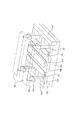
また、先行例1のメモリ装置の記憶素子3の断面図を図2に示す。
図2に示すように、この記憶素子3は、下層側から順に、下地層14、磁化固定層15、絶縁層16、記憶層17、キャップ層18が積層されている。
A cross-sectional view of the
As shown in FIG. 2, the
この場合、スピン注入により磁化M17の向きが反転する記憶層17に対して、下層に磁化固定層15を設けている。
スピン注入型磁化反転メモリにおいては、記憶層17の磁化M17と磁化固定層15の磁化M15の相対的な角度によって情報の「0」「1」を規定している。
記憶層17と磁化固定層15との間には、トンネルバリア層(トンネル絶縁層)となる絶縁層16が設けられ、記憶層17と磁化固定層15とにより、MTJ素子が構成されている。
また、磁化固定層15の下には下地層14が形成され、記憶層17の上にはキャップ層18が形成されている。
In this case, the magnetization fixed
In the spin injection type magnetization reversal memory, information “0” and “1” are defined by the relative angle between the magnetization M17 of the
An insulating
A
記憶層17は、磁化M17の方向が層面垂直方向に自由に変化する磁気モーメントを有する強磁性体から構成されている。磁化固定層15は、磁化M15が膜面垂直方向に固定された磁気モーメントを有する強磁性体から構成されている。
情報の記憶は一軸異方性を有する記憶層17の磁化の向きにより行う。書込みは、膜面垂直方向に電流を印加し、スピントルク磁化反転を起こすことにより行う。このように、スピン注入により磁化の向きが反転する記憶層17に対して、下層に磁化固定層15が設けられ、記憶層14の記憶情報(磁化方向)の基準とされる。
先行例1では、記憶層17、磁化固定層15としてはCo−Fe−Bを用いる。
特に、そのCo−Fe−Bの組成が、0≦Cox≦40、60≦Fey≦100、0<Bz≦30において、(Cox−Fey)100-z−Bzとする。
The
Information is stored according to the magnetization direction of the
In the first example, Co—Fe—B is used as the
In particular, when the composition of Co—Fe—B is 0 ≦ Co x ≦ 40, 60 ≦ Fe y ≦ 100, and 0 <B z ≦ 30, (Co x −Fe y ) 100−z −B z .
磁化固定層15は情報の基準であるので、記録や読み出しによって磁化の方向が変化してはいけないが、必ずしも特定の方向に固定されている必要はなく、記憶層17よりも保磁力を大きくするか、膜厚を厚くするか、あるいは磁気ダンピング定数を大きくして記憶層17よりも動きにくくすればよい。
磁化を固定する場合にはPtMn、IrMnなどの反強磁性体を磁化固定層15に接触させるか、あるいはそれらの反強磁性体に接触した磁性体をRu等の非磁性体を介して磁気的に結合させ、磁化固定層15を間接的に固定しても良い。
Since the magnetization fixed
When the magnetization is fixed, an antiferromagnetic material such as PtMn or IrMn is brought into contact with the magnetization fixed
先行例1においては、特に、記憶層17が受ける実効的な反磁界の大きさが記憶層17の飽和磁化量Msよりも小さくなるように、記憶素子3の記憶層17の組成が調整されていることを特徴とする。
即ち、前述したように、記憶層17の強磁性材料Co−Fe−B組成を選定し、記憶層17が受ける実効的な反磁界の大きさを低くして、記憶層17の飽和磁化量Msよりも小さくなるようにする。
In the first example, in particular, the composition of the
That is, as described above, the composition of the ferromagnetic material Co—Fe—B of the
さらに、先行例1において、中間層である絶縁層16を、酸化マグネシウム層とした場合には、磁気抵抗変化率(MR比)を高くすることができる。
このようにMR比を高くすることによって、スピン注入の効率を向上して、記憶層17の磁化M1の向きを反転させるために必要な電流密度を低減することができる。
Further, in the first example, when the insulating
By increasing the MR ratio in this way, the efficiency of spin injection can be improved, and the current density required for reversing the direction of the magnetization M1 of the
先行例1の記憶素子3は、下地層14からキャップ層18までを真空装置内で連続的に形成して、その後エッチング等の加工により記憶素子3のパターンを形成することにより、製造することができる。
The
上述の先行例1によれば、記憶素子3の記憶層17が、記憶層17が受ける実効的な反磁界の大きさが記憶層17の飽和磁化量Msよりも小さくなるように構成されているので、記憶層17が受ける反磁界が低くなっており、記憶層17の磁化M17の向きを反転させるために必要となる、書き込み電流量を低減することができる。
一方、記憶層17の飽和磁化量Msを低減しなくても書き込み電流量を低減することができるため、記憶層17の飽和磁化量Msを充分な量として、記憶層17の熱安定性を充分に確保することが可能になる。
According to the above first example, the
On the other hand, since the amount of write current can be reduced without reducing the saturation magnetization amount Ms of the
このように、情報保持能力である熱安定性を充分に確保することができるため、特性バランスに優れた記憶素子3を構成することができる。
これにより、動作エラーをなくして、記憶素子3の動作マージンを充分に得ることができ、記憶素子3を安定して動作させることができる。
従って、安定して動作する、信頼性の高いメモリ装置を実現することができる。
As described above, since the thermal stability as the information holding capability can be sufficiently ensured, the
As a result, an operation error can be eliminated, a sufficient operation margin of the
Therefore, a highly reliable memory device that operates stably can be realized.
また、書き込み電流を低減して、記憶素子3に書き込みを行う際の消費電力を低減することが可能になる。
従って、先行例1の記憶素子3によりメモリセルを構成した、メモリ装置全体の消費電力を低減することが可能になる。
In addition, it is possible to reduce the write current and reduce the power consumption when writing to the
Therefore, it becomes possible to reduce the power consumption of the entire memory device in which the memory cell is configured by the
従って、情報保持特性が優れた、安定して動作する信頼性の高いメモリ装置を実現することができ、記憶素子3を備えたメモリ装置において、消費電力を低減することができる。
Therefore, a highly reliable memory device that has excellent information retention characteristics and operates stably can be realized, and power consumption can be reduced in the memory device including the
また、図2に示した記憶素子3を備える、図1に示した構成のメモリ装置は、メモリ装置を製造する際に、一般の半導体MOS形成プロセスを適用できるという利点を有している。
従って、本実施の形態のメモリ装置を、汎用メモリとして適用することが可能になる。
Further, the memory device having the configuration shown in FIG. 1 including the
Therefore, the memory device of this embodiment can be applied as a general-purpose memory.
[1-3.先行例1に関する実験]
ここで、先行例1の記憶素子の構成において、具体的に記憶層17を構成する強磁性層の材料を選定することにより、記憶層が受ける実効的な反磁界の大きさを調整して、記憶素子の試料を作製し、その特性を調べた。
[1-3. Experiment on Prior Example 1]
Here, in the configuration of the memory element of the first example, the magnitude of the effective demagnetizing field received by the memory layer is adjusted by specifically selecting the material of the ferromagnetic layer that constitutes the
実際のメモリ装置には、図1に示したように、記憶素子3以外にもスイッチング用の半導体回路等が存在するが、ここでは、記憶層17の磁化反転特性を調べる目的で、記憶素子のみを形成したウェハにより検討を行った。
As shown in FIG. 1, an actual memory device includes a semiconductor circuit for switching in addition to the
〜実験1〜
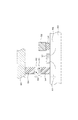
厚さ0.725mmのシリコン基板上に、厚さ300nmの熱酸化膜を形成し、その上に図2に示した構成の記憶素子3を形成した。
具体的には、図2に示した構成の記憶素子3において、各層の材料及び膜厚を図3に示すように選定した。
・下地層14:膜厚10nmのTa膜と膜厚25nmのRu膜の積層膜
・磁化固定層15:膜厚2.5nmのCoFeB膜
・トンネル絶縁層16:膜厚0.9nmの酸化マグネシウム膜
・記憶層17:磁化固定層と同じ組成のCoFeB膜
・キャップ層18:膜厚3nmのTa膜、膜厚3nmのRu膜、膜厚3nmのTa膜の積層膜
このように各層を選定し、また下地層14とシリコン基板との間に図示しない膜厚100nmのCu膜(後述するワード線となるもの)を設けた。
上記膜構成で、記憶層17の強磁性層は、材質をCo−Fe−Bの3元系合金とし、強磁性層の膜厚を2.0nmに固定した。
~
A thermal oxide film having a thickness of 300 nm was formed on a silicon substrate having a thickness of 0.725 mm, and the
Specifically, in the
-Underlayer 14: Laminated film of Ta film with a thickness of 10 nm and Ru film with a thickness of 25 nm-Magnetization fixed layer 15: CoFeB film with a thickness of 2.5 nm-Tunnel insulating layer 16: Magnesium oxide film with a thickness of 0.9 nm Memory layer 17: CoFeB film having the same composition as the magnetization fixed layer Cap layer 18: Laminated film of 3 nm thick Ta film, 3 nm thick Ru film, 3 nm thick Ta film Thus, each layer is selected, A Cu film (not shown) having a thickness of 100 nm (to be described later) was provided between the
With the above film configuration, the ferromagnetic layer of the
酸化マグネシウム膜から成る絶縁層16以外の各層は、DCマグネトロンスパッタ法を用いて成膜した。
酸化マグネシウム(MgO)膜から成る絶縁層16は、RFマグネトロンスパッタ法を用いて成膜した。
さらに、記憶素子3の各層を成膜した後に、磁場中熱処理炉で加熱処理を行った。
Each layer other than the insulating
The insulating
Further, after each layer of the
次に、ワード線部分をフォトリソグラフィによってマスクした後に、ワード線以外の部分の積層膜に対してArプラズマにより選択エッチングを行うことにより、ワード線(下部電極)を形成した。
この際に、ワード線部分以外は、基板の深さ5nmまでエッチングされた。
Next, after masking the word line portion by photolithography, the word line (lower electrode) was formed by performing selective etching with Ar plasma on the laminated film other than the word line.
At this time, except for the word line portion, the substrate was etched to a depth of 5 nm.
その後、電子ビーム描画装置により記憶素子3のパターンのマスクを形成し、積層膜に対して選択エッチングを行い、記憶素子3を形成した。記憶素子3部分以外は、ワード線のCu層直上までエッチングした。
なお、特性評価用の記憶素子には、磁化反転に必要なスピントルクを発生させるために、記憶素子に充分な電流を流す必要があるため、トンネル絶縁層の抵抗値を抑える必要がある。そこで、記憶素子3のパターンを、短軸0.09μm×長軸0.18μmの楕円形状として、記憶素子3の面積抵抗値(Ωμm2)が20Ωμm2となるようにした。
Thereafter, a mask of the pattern of the
In addition, in order to generate the spin torque necessary for the magnetization reversal, it is necessary to flow a sufficient current through the storage element for the characteristic evaluation storage element, and thus it is necessary to suppress the resistance value of the tunnel insulating layer. Therefore, the pattern of the
次に、記憶素子3部分以外を、厚さ100nm程度のAl2O3のスパッタリングによって絶縁した。
その後、フォトリソグラフィを用いて、上部電極となるビット線及び測定用のパッドを形成した。
このようにして、記憶素子3の試料を作製した。
Next, the portion other than the
Thereafter, a bit line to be an upper electrode and a measurement pad were formed using photolithography.
In this way, a sample of the
そして、上述の製造方法により、それぞれ記憶層17の強磁性層のCo−Fe−B合金の組成を変えた、記憶素子3の各試料を作製した。
Co−Fe−B合金の組成は、CoFeとBとの組成比(原子%)を80:20に固定して、CoFe中のCoの組成比x(原子%)を、90%、80%、70%、60%、50%、40%、30%、20%、10%、0%と変化させた。
Then, each sample of the
The composition of the Co—Fe—B alloy is such that the composition ratio (atomic%) of CoFe and B is fixed at 80:20, and the composition ratio x (atomic%) of Co in CoFe is 90%, 80%, It was changed to 70%, 60%, 50%, 40%, 30%, 20%, 10%, and 0%.
以上、作製した記憶素子3の各試料に対して、それぞれ以下のようにして、特性の評価を行った。
測定に先立ち、反転電流のプラス方向とマイナス方向の値を対称になるように制御することを可能にするため、記憶素子3に対して、外部から磁界を与えることができるように構成した。
また、記憶素子3に印加される電圧が、絶縁層16が破壊しない範囲内の1Vまでとなるように設定した。
As described above, the characteristics of each sample of the produced
Prior to the measurement, the
Further, the voltage applied to the
(飽和磁化量の測定)
飽和磁化量Msを、試料振動型磁力計(Vibrating Sample Magnetometer)を使用した、VSM測定によって、測定した。
(Measurement of saturation magnetization)
The saturation magnetization amount Ms was measured by VSM measurement using a vibrating sample magnetometer.
(実効的な反磁界の測定)
実効的な反磁界の測定用の試料として、上述した記憶素子3の試料とは別に、記憶素子3を構成する各層を形成し、これを20mm×20mm角の平面パターンに形成した試料を作製した。
そして、FMR(Ferromagnetic Resonance)測定によって、実効的な反磁界の大きさMeffectiveを求めた。
このFMR測定によって求められる、任意の外部磁場Hexに対する共鳴周波数fFMRは、下記の式(3)で与えられる。
(Measurement of effective demagnetizing field)
As a sample for measuring an effective demagnetizing field, a sample in which each layer constituting the
The effective demagnetizing field magnitude Meffective was determined by FMR (Ferromagnetic Resonance) measurement.
The resonance frequency fFMR obtained by this FMR measurement with respect to an arbitrary external magnetic field Hex is given by the following equation (3).
![]()
![]()
ここで、式(3)中のMeffectiveは、4πMeffective=4πMs−H⊥(H⊥:膜面に垂直な方向の異方性磁界)で表すことができる。 Here, Meffective in the formula (3) can be expressed by 4πMeffective = 4πMs−H⊥ (H⊥: an anisotropic magnetic field in a direction perpendicular to the film surface).
(反転電流値及び熱安定性の測定)
先行例1による記憶素子3の書き込み特性を評価する目的で、反転電流値の測定を行った。
記憶素子3に10μsから100msのパルス幅の電流を流して、その後の記憶素子3の抵抗値を測定した。
さらに、記憶素子3に流す電流量を変化させて、この記憶素子3の記憶層17の磁化M17の向きが反転する電流値を求めた。この電流値のパルス幅依存性をパルス幅1nsに外挿した値を、反転電流値とした。
また、反転電流値のパルス幅依存性の傾きは、記憶素子3の前述した熱安定性の指標(Δ)に対応する。反転電流値がパルス幅によって変化しない(傾きが小さい)ほど、熱の擾乱に強いことを意味する。
そして、記憶素子3間のばらつきを考慮するために、同一構成の記憶素子3を20個程度作製して、上述の測定を行い、反転電流値及び熱安定性の指標Δの平均値を求めた。
さらに、測定により得られた反転電流値の平均値と、記憶素子3の平面パターンの面積とから、反転電流密度Jc0を算出した。
(Measurement of reversal current value and thermal stability)
For the purpose of evaluating the writing characteristics of the
A current having a pulse width of 10 μs to 100 ms was passed through the
Furthermore, the amount of current flowing through the
Further, the inclination of the pulse width dependency of the inversion current value corresponds to the above-described thermal stability index (Δ) of the
Then, in order to take into account the variation between the
Further, the reversal current density Jc0 was calculated from the average value of the reversal current values obtained by the measurement and the area of the planar pattern of the
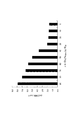
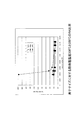
記憶素子3の各試料について、記憶層17のCo−Fe−B合金の組成と、飽和磁化量Ms及び実効的な反磁界の大きさMeffectiveの測定結果、さらに飽和磁化量と実効的な反磁界の大きさとの比Meffective/Msを表1に示す。ここで、表1に記載の記憶層17のCo−Fe−B合金のCo量は原子%で示している。
For each sample of the
表1から、(CoxFe100-x)80B20のCo量xが70%以下の場合においては、実効的な反磁界の大きさ(Meffective)は飽和磁化量Msよりも小さく、つまり、Co量xが70%以下のときの比Meffective/はMs、1.0より小さな値になっている。
さらに、Co量xが小さくなるほど、MeffectiveとMsの差が大きくなっていることが確認できる。
Table 1, in the (Co x Fe 100-x) 80 when the amount of Co (x) of B 20 is 70% or less, the level of effective demagnetizing field (Meffective) is smaller than the saturation magnetization amount Ms, that is, The ratio Meffective / when the Co amount x is 70% or less is smaller than Ms, 1.0.
Furthermore, it can be confirmed that the difference between Meffective and Ms increases as the Co amount x decreases.
反転電流値の測定結果を図4に示し、熱安定性の指標の測定結果を図5に示す。
図4は、記憶層17のCo−Fe−B合金のCo量x(CoFe中の含有量;原子%)と、反転電流値から求めた反転電流密度Jc0との関係を示している。
図5は、記憶層17のCo−Fe−B合金のCo量(CoFe中の含有量;原子%)と、熱安定性の指標Δ(KV/kBT)との関係を示している。
The measurement result of the reverse current value is shown in FIG. 4, and the measurement result of the thermal stability index is shown in FIG.
FIG. 4 shows the relationship between the Co amount x (content in CoFe; atomic%) of the Co—Fe—B alloy of the
FIG. 5 shows the relationship between the Co content of the Co—Fe—B alloy of the memory layer 17 (content in CoFe; atomic%) and the thermal stability index Δ (KV / k B T).
図4より、Co量xが小さくになるにつれて、反転電流密度Jc0が小さくなっていくことがわかる。
これは、Co量xが小さくなった場合、飽和磁化量Msは増加するが実効的な反磁界Meffectiveが小さくなるために、両者の積(Ms×Meffective)としては小さくなることに起因する。
FIG. 4 shows that the reversal current density Jc0 decreases as the Co amount x decreases.
This is because when the Co amount x decreases, the saturation magnetization amount Ms increases, but the effective demagnetizing field Meffective decreases, so that the product of both (Ms × Meffective) decreases.
図5より、Co量xが小さくなるにつれて、熱安定性の指標Δ(=KV/kBT)が大きくなっていき、Co量xがある程度以上小さくなると熱安定性の指標Δが大きい値で安定することが分かる。
これは、図5に示した飽和磁化量Msの測定結果と、式(2)より熱安定性の指標Δが飽和磁化量Msに比例することとから予想される変化とよく一致している。
From FIG. 5, as the Co amount x decreases, the thermal stability index Δ (= KV / k B T) increases, and when the Co amount x decreases to a certain extent, the thermal stability index Δ increases. It turns out to be stable.
This is in good agreement with the change expected from the measurement result of the saturation magnetization amount Ms shown in FIG. 5 and the fact that the thermal stability index Δ is proportional to the saturation magnetization amount Ms from the equation (2).
表1、図4、図5の結果より、実効的な反磁界Meffectiveが飽和磁化量Msよりも小さくなる、Co量xが70%以下の組成において、Msを下げるといった熱安定性を犠牲にする手法を用いずに、高い熱安定性を有したまま、反転電流値Jc0を低減できることが明らかになった。 From the results of Table 1, FIG. 4, and FIG. 5, the thermal destabilization is sacrificed in the composition in which the effective demagnetizing field Meffective is smaller than the saturation magnetization Ms and the Co content x is 70% or less. It has been clarified that the reversal current value Jc0 can be reduced without using a technique while maintaining high thermal stability.
〜実験2〜
上記の[実験1]により、(CoxFe100-x)80B20の場合、Co量xが70%以下の組成で高い熱安定性を有したまま、反転電流値Jc0を低減できることがわかった。
そこで、[実験2]において(Co70Fe30)80Bz、および(Co80Fe20)80Bz組成の記憶層17を用いて、B量zがCoとFeの比とMeffective/Msにどのような影響を与えるかを調べた。試料の詳細は[実験1]と同様である。
~
The
Therefore, in [Experiment 2], using the
表2に(Co70Fe30)100-zBzで、B量z(原子%)を5〜40%としたCoFeB合金の組成と、飽和磁化量Ms及び実効的な反磁界の大きさMeffectiveの測定結果、さらに飽和磁化量と実効的な反磁界の大きさとの比Meffective/Msを示す。
また表3には、(Co80Fe20)100-zBzの場合で、同様に、B量z(原子%)を5〜40%としたCoFeB合金の組成と、飽和磁化量Ms、実効的な反磁界の大きさMeffective、比Meffective/Msを示している。
Table 2 shows the composition of a CoFeB alloy with (Co 70 Fe 30 ) 100-z B z and a B amount z (atomic%) of 5 to 40%, a saturation magnetization amount Ms, and an effective demagnetizing field magnitude M effective. Further, the ratio Meffective / Ms between the saturation magnetization and the effective demagnetizing field is shown.
Table 3 also shows the composition of the CoFeB alloy in which the amount of B (z) (atomic%) is 5 to 40%, the saturation magnetization Ms, and the effective in the case of (Co 80 Fe 20 ) 100-z B z. The demagnetizing field magnitude Meffective and the ratio Meffective / Ms are shown.
表2の結果より、(Co70Fe30)100-zBzのようにCoとFeの比を70/30で固定した場合、B量z=40原子%以外の組成では実効的な反磁界Meffectiveが飽和磁化量Msより小さくなっていることが確認できる。 From the results of Table 2, when the ratio of Co and Fe is fixed at 70/30, such as (Co 70 Fe 30 ) 100-z B z , an effective demagnetizing field is obtained at a composition other than B content z = 40 atomic%. It can be confirmed that Meffective is smaller than the saturation magnetization Ms.
表3の結果より、(Co80Fe20)100-zBzのようにCoとFeの比を80/20で固定した場合、いずれの組成においても実効的な反磁界Meffectiveが飽和磁化量Msより大きくなっていることが確認できる。 From the results in Table 3, when the ratio of Co and Fe is fixed at 80/20 as in (Co 80 Fe 20 ) 100-z B z , the effective demagnetizing field Meffective is the saturation magnetization Ms in any composition. It can be confirmed that it is larger.
上述の表1〜3の結果より、B量zが30原子%以下の範囲であれば、飽和磁化量Msと実効的な反磁界Meffectiveの大小関係はCoとFeの比で決定されることが明らかになった。
従って、記憶層17の実効的な反磁界Meffectiveが飽和磁化量Msより小さくなるCo−Fe−B合金の組成は、
0≦Cox≦70、
30≦Fey≦100、
0<Bz≦30において、
(Cox−Fey)100-z−Bzである。
From the results of Tables 1 to 3, if the B amount z is in the range of 30 atomic% or less, the magnitude relationship between the saturation magnetization Ms and the effective demagnetizing field Meffective is determined by the ratio of Co and Fe. It was revealed.
Therefore, the composition of the Co—Fe—B alloy in which the effective demagnetizing field Meffective of the
0 ≦ Co x ≦ 70,
30 ≦ Fe y ≦ 100,
In 0 <B z ≦ 30,
It is (Co x -Fe y) 100- z -B z.
〜実験3〜
Gbitクラスのスピン注入型磁化反転メモリでは、記録素子のサイズが100nmφ以下になることが想定される。そこで、[実験3]において、50nmφのサイズの記録素子を用いて、熱安定性を評価した。
Co−Fe−B合金の組成は、CoFeとBとの組成比(原子%)を80:20に固定して、CoFe中のCoの組成比x(原子%)を、90%、80%、70%、60%、50%、40%、30%、20%、10%、0%と変化させた。
素子サイズ以外の試料の詳細は[実験1]と同様である。
~
In the Gbit class spin injection type magnetization reversal memory, it is assumed that the size of the recording element is 100 nmφ or less. Therefore, in [Experiment 3], thermal stability was evaluated using a recording element having a size of 50 nmφ.
The composition of the Co—Fe—B alloy is such that the composition ratio (atomic%) of CoFe and B is fixed at 80:20, and the composition ratio x (atomic%) of Co in CoFe is 90%, 80%, It was changed to 70%, 60%, 50%, 40%, 30%, 20%, 10%, and 0%.
Details of the sample other than the element size are the same as those in [Experiment 1].
記録素子3のサイズが50nmφの場合のCo−Fe−B合金のCo量(CoFe中の含有量;原子%)と熱安定性の指標Δ(KV/kBT)の関係を図6に示す。
FIG. 6 shows the relationship between the Co amount (content in CoFe; atomic%) of the Co—Fe—B alloy and the thermal stability index Δ (KV / k B T) when the size of the
図6より、素子サイズが50nmφになったことにより、熱安定性指数ΔのCo−Fe−B合金組成依存性が、図4に示した短軸0.09μm×長軸0.18μmの楕円形状記録素子で得られたΔのCo−Fe−B合金組成依存性から大きく変化したことが分かる。 As shown in FIG. 6, when the element size is 50 nmφ, the dependence of the thermal stability index Δ on the Co—Fe—B alloy composition is an elliptical shape with the minor axis 0.09 μm × major axis 0.18 μm shown in FIG. It can be seen that Δ greatly obtained from the Co—Fe—B alloy composition dependency of Δ obtained in the recording element.
図6によると、Feが60原子%以上存在するCo−Fe−B合金組成の場合にのみ、高い熱安定性が保持されている。
種々の検討を行った結果、Feが60原子%以上存在するCo−Fe−B合金が極微小な記録素子において高い熱安定性Δを示す理由は、Co−Fe−B合金の磁化が膜面面直方向を向いていることに起因していることが明らかになった。
Co−Fe−B合金の磁化が膜面面直方向になっている理由は、実効的な反磁界Meffectiveが飽和磁化量Msより著しく小さい組成であることに起因していると思われる。
また、垂直磁化膜になると極微小素子においても熱安定性が保たれる理由は、式(2)中のHk[実効的な異方性磁界]に関係しており、垂直磁化膜のHkは一般的に面内磁化膜よりも遥かに大きな値になる。つまり、垂直磁化膜では、大きなHkの効果により、面内磁化膜では十分な熱安定性Δを確保できない極微小な素子においても高い熱安定性Δを保つことが出来る。
上記の実験結果から、(CoxFe100-x)80B20という組成のCo−Fe−B合金では、Fe100-xが60以上になる場合、Gbitクラスのスピン注入を利用したメモリ装置に好適となるといえる。
According to FIG. 6, high thermal stability is maintained only in the case of a Co—Fe—B alloy composition in which Fe is present at 60 atomic% or more.
As a result of various studies, the reason why the Co—Fe—B alloy having Fe of 60 atomic% or more exhibits high thermal stability Δ in a very small recording element is that the magnetization of the Co—Fe—B alloy is the film surface. It became clear that it was caused by facing in the direction perpendicular to the surface.
The reason why the magnetization of the Co—Fe—B alloy is in the direction perpendicular to the film surface is considered to be due to the fact that the effective demagnetizing field Meffective is a composition significantly smaller than the saturation magnetization Ms.
In addition, the reason why the thermal stability is maintained even in a microelement when it is a perpendicular magnetization film is related to Hk [effective anisotropic magnetic field] in the equation (2), and the Hk of the perpendicular magnetization film is Generally, the value is much larger than that of the in-plane magnetization film. That is, in the perpendicular magnetization film, due to the effect of large Hk, high thermal stability Δ can be maintained even in a very small element that cannot secure sufficient thermal stability Δ in the in-plane magnetization film.
From the above experimental results, the (Co x Fe 100-x) 80 Co-Fe-B alloy having the composition of B 20, if the Fe 100-x is 60 or more, the memory device using the spin of Gbit class It can be said that it is preferable.
〜実験4〜
上記[実験3]において、(CoxFe100-x)80B20という組成のCo−Fe−B合金では、Fe量が60以上になる場合、Gbitクラスのスピン注入を利用したメモリ装置に好適となることを示した。[実験4]では、さらに、B量を5〜30原子%の範囲のCo−Fe−B合金で50nmφのサイズの記録素子を作製し、熱安定性を評価した。
素子サイズ以外の試料の詳細は[実験1]と同様である。
~
In the
Details of the sample other than the element size are the same as those in [Experiment 1].
Co量x=50、40、30、20、10、0およびB量z=5、10、20、30という範囲における(CoxFe100-x)100-zBzという組成のCo−Fe−B合金と熱安定性の指標Δ(KV/kBT)の関係を表4に示す。 Co—Fe— having a composition of (Co x Fe 100-x ) 100-z B z in the range of Co amount x = 50, 40, 30, 20, 10, 0 and B amount z = 5, 10, 20, 30 Table 4 shows the relationship between the alloy B and the thermal stability index Δ (KV / k B T).
表4より、Co量x=50かつB量z=5〜30の場合を除いたすべての組成において熱安定性Δが大きく保たれていることが分かる。
つまり、[実験4]の結果と同様に、Co量x=50と60がGbitクラスのスピン注入型磁化反転メモリに対応した極微小素子で高い熱安定性を確保する際の境界線になることが明らかになった。
From Table 4, it can be seen that the thermal stability Δ is largely maintained in all compositions except for the case where the Co amount x = 50 and the B amount z = 5-30.
That is, similar to the result of [Experiment 4], the Co amount x = 50 and 60 becomes the boundary line when ensuring high thermal stability in a micro device corresponding to the Gbit class spin-injection type magnetization reversal memory. Became clear.
従って、上記の結果より、記憶層17のCo−Fe−B合金の組成が、
0≦Cox≦40、
60≦Fey≦100、
0<Bz≦30において、
(Cox−Fey)100-z−Bzである場合、Gbitクラスのスピン注入型磁化反転メモリを作製するのに好適であることが判明した。
Therefore, from the above results, the composition of the Co—Fe—B alloy of the
0 ≦ Co x ≦ 40,
60 ≦ Fe y ≦ 100,
In 0 <B z ≦ 30,
(Co x -Fe y) when a 100-z -B z, it is preferable to make the spin-injection magnetization inversion memory of Gbit class has been found.
なおCo−Fe−B合金は、CoとFe比のFeが大きい組成において、実効的な反磁界Meffectiveと飽和磁化量Msの乖離が大きくなり、垂直磁化し易くなるため、熱安定性が確保し易くなる。
そのため、磁気メモリの容量が増加し、記憶素子3のサイズが小さくなったときはFeを多く含むCo−Fe−B合金の方が熱安定性を確保し易くなる。
そこで、例えば、Feyが60、70nmφの記憶層17でGbitクラスのスピン注入型磁気メモリが実現できている状況を考えると、記憶素子3の直径が5nmφ小さくなる毎にCo−Fe−B合金のFe量yは5ずつ増えた状態になっていることが望ましい。
例えばFe量yは、上記の(Cox−Fey)100-z−Bzの場合において、CoFe中の含有量としての原子%が65%、70%、75%、80%・・・という組成とする(Co量xでいえば、35%,30%,25%,20%・・・とする)ことが、記憶素子サイズの縮小に応じてより好適な例となる。
Note that the Co—Fe—B alloy has a large Co / Fe ratio Fe, and the difference between the effective demagnetizing field Meffective and the saturation magnetization Ms becomes large, and it becomes easy to perform perpendicular magnetization, thus ensuring thermal stability. It becomes easy.
Therefore, when the capacity of the magnetic memory is increased and the size of the
Thus, for example, considering the situation where a Gbit class spin-injection type magnetic memory can be realized with the
For example Fe amount y, in case of the above (Co x -Fe y) 100- z -B z, atomic% as the content in the CoFe 65%, 70%, 75%, of 80%.. A composition (in terms of Co amount x, 35%, 30%, 25%, 20%,...) Is a more preferable example in accordance with the reduction in the memory element size.
[1-4.先行例2の構成]
続いて、先行例2について説明する。なお、先行例2のメモリ装置及び記憶素子3の構成例は図1,図2と同様であるため、その重複説明は避ける。
この先行例2は、先行例1と同じく、記憶層17、磁化固定層15としてCo−Fe−Bを用いるが、そのCo−Fe−Bの組成が、0≦Cox≦40、60≦Fey≦100、20<Bz≦40において、(Cox−Fey)100-z−Bzとするものである。
[1-4. Configuration of Prior Example 2]
Then, the prior example 2 is demonstrated. The configuration examples of the memory device and the
As in the preceding example 1, the preceding example 2 uses Co—Fe—B as the
半導体デバイスであるスピン注入型磁化反転メモリの製造を考えた場合、記憶素子3を構成する磁性材料は半導体プロセスが許容する温度範囲で優れた特性を発揮することが望まれる。
例えば、Si基板からすべての工程を経て、チップになるまでの間に行われる半導体プロセスで加わる熱負荷は、350度以上になることがあるため、それを考慮すると、記憶素子3を構成する磁性材料は350度以上の熱処理をしたときでも優れた特性になる必要がある。
また、他方、メモリ装置の動作に必要なトランジスタは通常、例えば450度以上の高温にさらされると特性が劣化してしまう。このため450度、500度などの高温で加熱した状態で優れた特性を示す磁性材料も好適ではない。
Considering the manufacture of a spin-injection magnetization reversal memory that is a semiconductor device, it is desirable that the magnetic material constituting the
For example, since the thermal load applied in the semiconductor process performed from the Si substrate through all the steps until it becomes a chip may be 350 degrees or more, the magnetic elements constituting the
On the other hand, the characteristics of the transistors necessary for the operation of the memory device are usually deteriorated when exposed to a high temperature of, for example, 450 degrees or more. For this reason, the magnetic material which shows the outstanding characteristic in the state heated at high temperature, such as 450 degree | times and 500 degree | times, is not suitable.
したがって、スピン注入型磁化反転メモリの製造を考えた場合、記憶素子3を構成する磁性材料は概ね350度以上から450度未満程度の温度範囲で良好な特性を示すことが必要である。
Therefore, when manufacturing a spin-injection type magnetization reversal memory is considered, the magnetic material constituting the
半導体プロセスとの熱的な親和性の観点から考えると、一般的な垂直磁化材料は250度以上の高温で磁気およびTMR特性を劣化させる、もしくは500度以上の高温において磁気特性が出現することが多いため、垂直磁化膜は取り扱いが難しい。
しかしながら、上述のように垂直磁化膜は大容量、低消費電力化に適している。従って、半導体プロセスと親和性の高い熱処理条件で低反転電流かつ高出力な特性を示すスピン注入型磁化反転メモリ用の垂直磁化膜を開発することは重要である。
そこで先行例2は、上述のように大容量、低消費電力化に適した垂直磁気異方性を有する記録素子3を用いたメモリ装置において、熱処理温度が350度以上、450度未満の範囲で大きな磁気抵抗変化率を確保する必要がある、という認識に基づくものである。
From the viewpoint of thermal compatibility with a semiconductor process, a general perpendicular magnetization material may deteriorate magnetic and TMR characteristics at a high temperature of 250 degrees or higher, or may exhibit magnetic characteristics at a high temperature of 500 degrees or higher. Since there are many, a perpendicular magnetization film is difficult to handle.
However, as described above, the perpendicular magnetization film is suitable for large capacity and low power consumption. Therefore, it is important to develop a perpendicular magnetization film for a spin-injection type magnetization reversal memory that exhibits low reversal current and high output characteristics under heat treatment conditions that are highly compatible with semiconductor processes.
Therefore, in the second example, in the memory device using the
上述のように記録電流を低減させるためには、垂直磁化型を採用することが望ましい。また垂直磁化膜は一般に面内磁化膜よりも高い磁気異方性を持たせることが可能であるため、上述の熱安定性Δを大きく保つ点でも好ましい。 In order to reduce the recording current as described above, it is desirable to adopt the perpendicular magnetization type. Further, since the perpendicular magnetization film can generally have a higher magnetic anisotropy than the in-plane magnetization film, it is also preferable from the viewpoint of keeping the above-described thermal stability Δ large.
垂直異方性を有する磁性材料には希土類−遷移金属合金(TbCoFeなど)、金属多層膜(Co/Pd多層膜など)、規則合金(FePtなど)、酸化物と磁性金属の間の界面異方性の利用(Co/MgOなど)等いくつかの種類がある。しかし、希土類−遷移金属合金は加熱により拡散、結晶化すると垂直磁気異方性を失うため、スピン注入型磁化反転メモリ用材料としては好ましくない。また金属多層膜も加熱により拡散し、垂直磁気異方性が劣化することが知られており、さらに垂直磁気異方性が発現するのは面心立方の(111)配向となっている場合であるため、MgOやそれに隣接して配置するFe、CoFe、CoFeBなどの高分極率層に要求される(001)配向を実現させることが困難となる。
L10規則合金は高温でも安定であり、かつ(001)配向時に垂直磁気異方性を示すことから、上述のような問題は起こらないものの、製造時に500℃以上の十分に高い温度で加熱する、あるいは製造後に500℃以上の高温で熱処理を行うことで原子を規則配列させる必要があり、半導体プロセスとの親和性が低い。かつ、トンネルバリア等積層膜の他の部分における好ましくない拡散や界面粗さの増大を引き起こす可能性がある。
Magnetic materials having perpendicular anisotropy include rare earth-transition metal alloys (such as TbCoFe), metal multilayer films (such as Co / Pd multilayer films), ordered alloys (such as FePt), and interface anisotropy between oxides and magnetic metals. There are several types such as utilization of sex (Co / MgO etc.). However, since rare earth-transition metal alloys lose perpendicular magnetic anisotropy when they are diffused and crystallized by heating, they are not preferred as materials for spin-injection magnetization reversal memories. In addition, it is known that metal multilayer film diffuses by heating and the perpendicular magnetic anisotropy deteriorates. Further, the perpendicular magnetic anisotropy is manifested in the case of a face-centered cubic (111) orientation. Therefore, it is difficult to realize the (001) orientation required for high polarizability layers such as MgO and Fe, CoFe, CoFeB arranged adjacent to MgO.
The L10 ordered alloy is stable even at high temperatures and exhibits perpendicular magnetic anisotropy during (001) orientation, so that the above-mentioned problems do not occur, but it is heated at a sufficiently high temperature of 500 ° C. or higher during production. Alternatively, it is necessary to arrange the atoms regularly by performing a heat treatment at a high temperature of 500 ° C. or higher after manufacture, and the affinity with the semiconductor process is low. In addition, it may cause undesirable diffusion and increase in interface roughness in other portions of the laminated film such as a tunnel barrier.
これに対し、界面磁気異方性を利用した材料、すなわちトンネルバリアであるMgO上にCo系あるいはFe系材料を積層させたものは上記いずれの問題も起こり難く、このためスピン注入型磁化反転メモリの記憶層材料として有望視されている。 On the other hand, a material using interfacial magnetic anisotropy, that is, a layer in which a Co-based or Fe-based material is laminated on MgO, which is a tunnel barrier, is unlikely to cause any of the above problems. It is regarded as a promising memory layer material.
そこで、本願の発明者等が種々の検討を行った結果、Co−Fe−Bで構成される磁性材料であり、組成が0≦Cox≦40、60≦Fey≦100、20<Bz≦40、[(Cox−Fey)100-z−Bz]の範囲にある場合、熱処理温度を350度以上にした状態でも、上記の反転電流を表す式中のスピン分極率Pを高く保つことが出来ることを見出した。
高出力素子はスピン分極率Pが高いことから、このような先行例2によれば低反転電流化も可能である。
さらに、高い磁気異方性を有する垂直磁化材料を用いることで、熱安定性を犠牲にすることなく、高出力かつ低消費電力なスピン注入型の磁化反転素子(記憶素子3)が提供可能になる。
Therefore, as a result of various studies by the inventors of the present application, the magnetic material is composed of Co—Fe—B, and the composition is 0 ≦ Co x ≦ 40, 60 ≦ Fe y ≦ 100, 20 <B z. ≦ 40, [(Co x -Fe y) 100-z -B z] If the range of, even in a state where the heat treatment temperature above 350 degrees, a high spin polarization P in the formula representing the switching current I found that I can keep it.
Since the high output element has a high spin polarizability P, according to the preceding example 2, a low inversion current can be achieved.
Furthermore, by using a perpendicular magnetization material having high magnetic anisotropy, it is possible to provide a spin-injection type magnetization reversal element (memory element 3) with high output and low power consumption without sacrificing thermal stability. Become.
先行例2のメモリ装置及び記憶素子3の構成は、上記図1,図2と同様であるが、記憶素子3の記憶層17が上記組成のものとなる。
つまり先行例2の記録素子によれば、情報を磁性体の磁化状態により保持する記憶層17を有し、記憶層17に対して、中間層である絶縁層16を介して磁化固定層15が設けられる。そして積層方向にスピン偏極した電子を注入することにより、膜面垂直方向に磁化した記憶層17の磁化の向きが変化して、記憶層17に対して情報の記録が行われる。ここで記憶層17を構成する強磁性層材料として例えば上記組成のCo−Fe−Bを用いることにより、高温熱処理でも高いトンネル磁気抵抗効果かつ低反転電流の特性を得ることができる。
これにより高温熱処理でも高出力、かつ低電流での磁化反転を可能とする。
The configuration of the memory device and the
That is, according to the recording element of the prior example 2, the
This enables magnetization reversal at high output and low current even during high-temperature heat treatment.
またこの記憶素子3を用いたメモリ装置は、2種類の配線(図1の配線1,6)を通じて、記憶素子3に積層方向の電流が流れ、スピントランスファが起こることにより、2種類の配線を通じて記憶素子3の積層方向に電流を流してスピントルク磁化反転による情報の記録を行うことができる。
Further, in the memory device using the
このような先行例2では、高温熱処理でも高出力かつ低電流動作といった特性が得られるため、特性バランスに優れた記憶素子3を構成することができる。
また、高い磁気異方性を有する垂直磁化膜を用いているため、情報の熱安定性が低下することも無い。
これにより、動作エラーをなくして、記憶素子3の動作マージンを充分に得ることができ、記憶素子3を安定して動作させることができる。
また、350度以上450度未満の高温熱処理ですぐれた特性を示す材料であるため、半導体プロセスとの親和性が高い。
また、記録素子3に対する書き込み電流が低減されることにより、記録素子の消費電力を低減することが可能となる
従って、先行例2の記憶素子3によりメモリセルを構成した、メモリ全体の消費電力を低減することが可能になる。
従って、安定して動作する、信頼性の高いメモリを実現することができる。
In the preceding example 2, since the characteristics such as high output and low current operation can be obtained even by high-temperature heat treatment, it is possible to configure the
Further, since a perpendicular magnetization film having high magnetic anisotropy is used, the thermal stability of information is not lowered.
As a result, an operation error can be eliminated, a sufficient operation margin of the
In addition, since it is a material that exhibits excellent characteristics by high-temperature heat treatment at 350 ° C. or higher and lower than 450 ° C., it has a high affinity with semiconductor processes.
Further, since the write current to the
Therefore, a highly reliable memory that operates stably can be realized.
また、図2に示した記憶素子3を備える、図1に示した構成のメモリは、メモリを製造する際に、一般の半導体MOS形成プロセスを適用できるという利点を有している。
従って、本例のメモリを、汎用メモリとして適用することが可能になる。
なお磁化固定層15についても、上記組成のCo−Fe−Bとしてもよい。
The memory having the
Therefore, the memory of this example can be applied as a general-purpose memory.
The fixed
また先行例2においても、中間層である絶縁層16を、酸化マグネシウム層とした場合には、磁気抵抗変化率(MR比)を高くすることができる。
MR比を高くすることによって、スピン注入の効率を向上して、記憶層17の磁化M17の向きを反転させるために必要な電流密度をさらに低減することができる。
Also in the prior example 2, when the insulating
By increasing the MR ratio, the efficiency of spin injection can be improved and the current density required to reverse the direction of the magnetization M17 of the
また記憶素子3は、下地層14からキャップ層18までを真空装置内で連続的に形成して、その後エッチング等の加工により記憶素子3のパターンを形成することにより、製造することができる。
In addition, the
[1-5.先行例2に関する実験]
ここで、先行例としての記憶素子3の構成において、具体的に記憶層17を構成する強磁性層の材料を選定し、記憶素子3の特性を調べた。
上述の[実験1]〜[実験4]と同様、記憶層17の磁化反転特性を調べる目的で、記憶素子3のみを形成したウェハにより検討を行った。
[1-5. Experiment on Prior Example 2]
Here, in the configuration of the
As in the above [Experiment 1] to [Experiment 4], for the purpose of investigating the magnetization reversal characteristics of the
〜実験5〜
厚さ0.725mmのシリコン基板上に、厚さ300nmの熱酸化膜を形成し、その上に図2に示した構成の記憶素子3を図7に示すように形成した。
・下地層14:膜厚10nmのTa膜と膜厚10nmのRu膜と膜厚10nmのTa膜の積層膜
・磁化固定層15:膜厚1.2nmのCoFeB膜
・トンネル絶縁層16:膜厚0.9nmの酸化マグネシウム膜
・記憶層17:磁化固定層と同じ組成のCoFeB膜
・キャップ層18:膜厚3nmのTa膜、膜厚3nmのRu膜、膜厚3nmのTa膜の積層膜
このように各層を選定し、また下地膜14とシリコン基板との間に図示しない膜厚100nmのCu膜(後述するワード線となるもの)を設けて、各層を形成した。
上記膜構成で、記憶層17の強磁性層は、材質をCo−Fe−Bの3元系合金とし、強磁性層の膜厚を1.5nmに固定した。
~
A thermal oxide film having a thickness of 300 nm was formed on a silicon substrate having a thickness of 0.725 mm, and the
Underlayer 14: Laminated film of 10 nm thick Ta film, 10 nm thick Ru film, and 10 nm thick Ta film Magnetization fixed layer 15: 1.2 nm thick CoFeB film Tunnel insulating layer 16: Thickness 0.9 nm magnesium oxide film Memory layer 17: CoFeB film having the same composition as the magnetization fixed layer Cap layer 18: Laminated film of 3 nm thick Ta film, 3 nm thick Ru film, 3 nm thick Ta film Each layer was selected as described above, and a Cu film (not shown) having a thickness of 100 nm (to be described later) was formed between the
With the above film configuration, the ferromagnetic layer of the
酸化マグネシウム膜から成る絶縁層16以外の各層は、DCマグネトロンスパッタ法を用いて成膜した。
酸化マグネシウム(MgO)膜から成る絶縁層16は、RFマグネトロンスパッタ法を用いて成膜した。
さらに、記憶素子3の各層を成膜した後に、磁場中熱処理炉で、各種温度・1時間の熱処理を行った。
Each layer other than the insulating
The insulating
Further, after each layer of the
次に、ワード線部分をフォトリソグラフィによってマスクした後に、ワード線以外の部分の積層膜に対してArプラズマにより選択エッチングを行うことにより、ワード線(下部電極)を形成した。この際に、ワード線部分以外は、基板の深さ5nmまでエッチングされた。 Next, after masking the word line portion by photolithography, the word line (lower electrode) was formed by performing selective etching with Ar plasma on the laminated film other than the word line. At this time, except for the word line portion, the substrate was etched to a depth of 5 nm.
その後、電子ビーム描画装置により記憶素子3のパターンのマスクを形成し、積層膜に対して選択エッチングを行い、記憶素子3を形成した。記憶素子3部分以外は、ワード線のCu層直上までエッチングした。
なお、特性評価用の記憶素子には、磁化反転に必要なスピントルクを発生させるために、記憶素子に充分な電流を流す必要があるため、トンネル絶縁層の抵抗値を抑える必要がある。そこで、記憶素子3のパターンを、短軸0.09μm×長軸0.09μmの楕円形状として、記憶素子3の面積抵抗値(Ωμm2)が20Ωμm2となるようにした。
Thereafter, a mask of the pattern of the
In addition, in order to generate the spin torque necessary for the magnetization reversal, it is necessary to flow a sufficient current through the storage element for the characteristic evaluation storage element, and thus it is necessary to suppress the resistance value of the tunnel insulating layer. Therefore, the pattern of the
次に、記憶素子3部分以外を、厚さ100nm程度のAl2O3のスパッタリングによって絶縁した。
その後、フォトリソグラフィを用いて、上部電極となるビット線及び測定用のパッドを形成した。
このようにして、記憶素子3の試料を作製した。
Next, the portion other than the
Thereafter, a bit line to be an upper electrode and a measurement pad were formed using photolithography.
In this way, a sample of the
そして、上述の製造方法により、それぞれ記憶層17の強磁性層のCo−Fe−B合金の組成を変えた、記憶素子3の各試料を作製した。
Co−Fe−B合金の組成は、CoとFeの組成比(原子%)を20:80に固定して、Bの組成比z(原子%)を、10%、20%、30%、35%、40%、50%と変化させた。
Then, each sample of the
The composition of the Co—Fe—B alloy is such that the composition ratio (atomic%) of Co and Fe is fixed at 20:80, and the composition ratio z (atomic%) of B is 10%, 20%, 30%, 35 %, 40%, and 50%.
以上、作製した記憶素子3の各試料に対して、それぞれ以下のようにして、特性の評価を行った。
(TMRの測定)
先行例の記憶素子の出力特性を評価する目的で、TMRの測定を行った。
記憶素子3に磁場を3kOeの範囲で掃印しながら100mVの電圧を印加し、記憶素子3の抵抗値を測定した。
そして、記憶素子3間のばらつきを考慮するために、同一構成の記憶素子3を20個程度作製して、上述の測定を行い、特性の平均値を求めた。
As described above, the characteristics of each sample of the produced
(Measurement of TMR)
TMR was measured for the purpose of evaluating the output characteristics of the memory element of the preceding example.
A voltage of 100 mV was applied to the
Then, in order to take into account the variation between the
記憶素子3の各試料について、図8に記憶層17のCo−Fe−B合金の組成毎にTMRの熱処理温度依存性を示す。
図8より、B濃度が10%の場合[図中の10B]、TMRは熱処理温度:300度付近でピークを取っていることが分かる。
これに対して、B濃度が20〜40%の組成範囲の場合[図中の20B〜40B]、TMRのピークが熱処理温度350〜400度付近へとシフトしている。
また、B濃度が50%の場合[図中の50B]、200度以上の熱処理になると、TMRが観測されるようになるものの、TMRの絶対値が他の組成のCo−Fe−B合金と比較して極端に小さくなっていることが分かる。
B濃度が40%の場合、B濃度が10〜35%の試料の最大TMR[110%程度]と比較して、若干小さなTMRにとどまっているが、熱処理温度350〜400度付近で約80%程度のTMRは確保されており、スピン注入型磁化反転メモリに適応可能な出力に達している。
またB濃度が20〜30%の試料では450度付近でも十分なTMRが確保されている。
For each sample of the
From FIG. 8, it can be seen that when the B concentration is 10% [10B in the figure], TMR has a peak at a heat treatment temperature of about 300 degrees.
In contrast, when the B concentration is in the composition range of 20 to 40% [20B to 40B in the figure], the TMR peak shifts to a heat treatment temperature of around 350 to 400 degrees.
Further, when the B concentration is 50% [50B in the figure], TMR is observed when heat treatment is performed at 200 ° C. or more, but the absolute value of TMR is different from that of Co—Fe—B alloys having other compositions. It can be seen that it is extremely small in comparison.
When the B concentration is 40%, the TMR is slightly smaller than the maximum TMR of the sample having the B concentration of 10 to 35% [about 110%], but about 80% at a heat treatment temperature of about 350 to 400 degrees. TMR of a certain degree is secured, and an output that can be applied to the spin-injection type magnetization reversal memory has been reached.
In addition, sufficient TMR is secured even in the vicinity of 450 ° C. for samples having a B concentration of 20 to 30%.
結論として、B濃度が20〜40%の組成範囲の場合、半導体プロセスと最も適合する熱処理範囲において、最も良好なTMR特性が得られることが確認できる。
一般に、Co−Fe−B合金を用いてトンネル磁気接合を作る場合、熱処理によりBがMgOバリア(絶縁層16)もしくはキャップ層18側に拡散することが知られている。熱処理温度350度〜400度の範囲でB濃度が20〜40%が好適となる理由は、このBの拡散と関係しており、初期のCo−Fe−B合金組成としてある一定量のBを合金膜中に存在させることにより、所望の熱処理温度範囲で優れた垂直磁気特性ならびにTMR特性が得られるBの分布が実現し、それに伴いMgOバリアとCo−Fe−B合金の界面磁気異方性を強化したためと予想される。
As a conclusion, it can be confirmed that when the B concentration is in the composition range of 20 to 40%, the best TMR characteristics can be obtained in the heat treatment range most suitable for the semiconductor process.
In general, when making a tunnel magnetic junction using a Co—Fe—B alloy, it is known that B diffuses to the MgO barrier (insulating layer 16) or the
この予想によると、450度以上の高温熱処理でも優れたTMR特性が得られるB濃度が存在することになるが、本実験で用いた試料の場合、450度を越える熱処理では下地層14のラフネスが増大し、さらに過度な下地層14、キャップ層18の拡散が生じたため、すべてのB濃度のCo−Fe−BでTMR特性が劣化したものと考えられる。
According to this expectation, there is a B concentration that can provide excellent TMR characteristics even at a high temperature heat treatment of 450 ° C. or more. However, in the case of the sample used in this experiment, the roughness of the
B濃度が10%の場合、350度以上の高温でTMR特性が劣化した原因は、高温で熱処理した場合にはB濃度が少なすぎるため、MgOバリアとCo−Fe−B合金の界面磁気異方性を強化することが出来ないことに起因すると考えられる。
また、B濃度が50%の場合に良好なTMR特性が得られない原因は、B濃度が高すぎで飽和磁化が極端に低下したためと推察される。
When the B concentration is 10%, the cause of the deterioration of the TMR characteristics at a high temperature of 350 ° C. or more is that the B concentration is too low when the heat treatment is performed at a high temperature. This is thought to be due to the inability to enhance sex.
Further, it is assumed that the reason why good TMR characteristics cannot be obtained when the B concentration is 50% is that the saturation magnetization is extremely lowered due to the B concentration being too high.
以上の結果より、CoとFeの組成比(原子%)を20:80に固定したCo−Fe−B合金の場合、B濃度が20〜40%で熱処理温度350度〜450度の範囲で高出力な記録素子3を作成できることが実証された。
From the above results, in the case of the Co—Fe—B alloy in which the composition ratio (atomic%) of Co and Fe is fixed at 20:80, the B concentration is 20 to 40% and the heat treatment temperature is high in the range of 350 to 450 degrees. It was demonstrated that an
〜実験6〜
上記の[実験5]では、特定のCo/Fe比でB濃度を変えた場合の詳細な実験結果を示した。次に、[実験6]ではCo/Fe比を40/60、30/70、10/90として、B濃度をそれぞれ20%、30%、40%と変化させた記録素子17を作成し、TMR特性の評価を行った。
~ Experiment 6 ~
In the above [Experiment 5], detailed experimental results when the B concentration was changed at a specific Co / Fe ratio were shown. Next, in [Experiment 6], the
図9(a)(b)(c)に、各Co/Fe比でB濃度および熱処理温度を変えた場合のTMR特性を示す。
この結果からわかるように、いずれの組成においても[実験5]で示したB濃度[20〜40%]、熱処理範囲[350度〜400度]において、高出力[=高TMR]となる特性が得られている。
また450度付近でも高出力[=高TMR]となる組成も見られる。例えばB濃度が20〜30%の組成である。
また、TMRの値に、Co/Fe比に対する大きな依存性は観測されない。
FIGS. 9A, 9B, and 9C show the TMR characteristics when the B concentration and the heat treatment temperature are changed at each Co / Fe ratio.
As can be seen from this result, in any composition, the B concentration [20 to 40%] and the heat treatment range [350 to 400 degrees] shown in [Experiment 5] have the characteristics of high output [= high TMR]. Has been obtained.
In addition, a composition having a high output [= high TMR] is observed even at around 450 degrees. For example, the B concentration is 20 to 30%.
In addition, no great dependence on the Co / Fe ratio is observed in the TMR value.
以上の[実験5]および[実験6]の結果により、組成が0≦Cox≦40、60≦Fey≦100、20<Bz≦40において、(Cox−Fey)100-z−Bzとなる垂直磁化強磁性材料Co−Fe−Bを用いることにより、半導体プロセスと親和性の高い熱処理温度範囲:350度〜400度で高出力な記録素子が提供可能であることが示される。
また、高出力を実現したことにより、高いスピン分極率Pも同時に実現することによって、低消費電力化も可能となる。
このように垂直磁化の高い磁気異方性を活用することによって熱安定性を犠牲にする手法を用いることなく、高出力かつ低反転電流のスピン注入磁化反転素子が提供可能になった。
The results of the above Experiment 5] and [Experiment 6], in the composition 0 ≦ Co x ≦ 40,60 ≦ Fe y ≦ 100,20 <B z ≦ 40, (Co x -Fe y) 100-z - It is shown that by using the perpendicular magnetization ferromagnetic material Co—Fe—B that becomes B z , it is possible to provide a high-power recording element in a heat treatment temperature range: 350 ° to 400 ° that is highly compatible with a semiconductor process. .
Further, by realizing a high output, a high spin polarizability P can be realized at the same time, thereby reducing the power consumption.
Thus, a spin-injection magnetization reversal element having a high output and a low reversal current can be provided without using a method of sacrificing thermal stability by utilizing magnetic anisotropy with high perpendicular magnetization.
なお、前述の先行例1では、B濃度については、0<Bz≦30の範囲で実効的な反磁界Meffectiveが飽和磁化量Msより小さくなり、垂直磁化に好適であると述べた。(例えば上記表2参照)。これに対し、先行例2ではB濃度について20<Bz≦40とするものであるが、すると30〜40%の範囲は、適切でないように見える。
しかしながら、比較的高温の熱処理を行う場合、B濃度が30〜40%の範囲も、実効的な反磁界Meffectiveが飽和磁化量Msより小さくなり、垂直磁化に好適であることがわかった。
In the above-mentioned prior example 1, it has been described that the effective demagnetizing field Meffective is smaller than the saturation magnetization amount Ms in the range of 0 <B z ≦ 30 with respect to the B concentration, which is suitable for perpendicular magnetization. (See, for example, Table 2 above). On the other hand, in the prior example 2, the B concentration is set to 20 <B z ≦ 40, but the range of 30 to 40% seems to be inappropriate.
However, when a relatively high temperature heat treatment is performed, it has been found that the effective demagnetizing field Meffective is smaller than the saturation magnetization amount Ms even when the B concentration is in the range of 30 to 40%, which is suitable for perpendicular magnetization.
以下の[表5]は、記憶層17のCo−Fe−B組成が、(Co70−Fe30)65−B35と、(Co70−Fe30)60−B40の場合について、熱処理温度を400℃とした場合の飽和磁化量Msと実効的な反磁界Meffectiveについて調べたものである。
[Table 5] below shows the heat treatment temperature when the Co—Fe—B composition of the
B濃度が35%、40%のいずれの場合も、実効的な反磁界Meffectiveが飽和磁化量Msより小さく(Meffective/Ms<1)なっている。
つまり、熱処理温度が高い場合、B濃度が30〜40%の範囲でも、記憶層17が受ける、実効的な反磁界の大きさが、記憶層17の飽和磁化量よりも小さいということを満たしているものとなる。
When the B concentration is 35% or 40%, the effective demagnetizing field Meffective is smaller than the saturation magnetization Ms (Meffective / Ms <1).
That is, when the heat treatment temperature is high, even when the B concentration is in the range of 30 to 40%, the effective demagnetizing field received by the
<2.実施の形態の記憶素子>
[2-1.先行例の課題について]
先行例においては、記憶層17の強磁性材料としてCo−Fe−B合金を用い、その組成を所定の比率とすることで、書き込み電流量の低減と、情報保持能力である熱安定性の点で好適な記憶素子を実現できることについて触れた。
ただし、このようにCo−Fe−B合金を用いる場合においては、記憶層17の強磁性層の組成としてFeを比較的多く含むものとなる。
このことによると、磁気メモリの製造プロセス時の加工ダメージ・高温加熱において、酸化、つまりは腐食による抵抗の上昇が促進されてしまうこととなる。
<2. Memory Element of Embodiment>
[2-1. About the problem of the previous example]
In the preceding example, a Co—Fe—B alloy is used as the ferromagnetic material of the
However, when the Co—Fe—B alloy is used as described above, the composition of the ferromagnetic layer of the
According to this, in the processing damage and high temperature heating during the manufacturing process of the magnetic memory, an increase in resistance due to oxidation, that is, corrosion is promoted.
特に、素子直径を100nm以下に微細化することが要求される高密度記憶素子では、外周部からの磁性層への侵食による抵抗上昇が無視できなくなる。加工方法によって、MgOトンネルバリア膜の直上でエッチングを止めて、下部・磁化固定層を保護する方法も存在するが、上部・記憶層については変わらず磁性体が露出するものとなってしまう。 In particular, in a high-density memory element that is required to be miniaturized to an element diameter of 100 nm or less, an increase in resistance due to erosion of the magnetic layer from the outer peripheral portion cannot be ignored. Depending on the processing method, there is a method in which etching is stopped immediately above the MgO tunnel barrier film to protect the lower / magnetization pinned layer, but the upper / memory layer remains the same without exposing the magnetic material.
本実施の形態の目的は、記憶層の耐食性を強化し、微細加工時の抵抗上昇を防止する比較的容易な方法を提案し、安定かつ低電流で記録可能なST−MRAM素子を提供することにある。 An object of the present embodiment is to propose a relatively easy method for enhancing the corrosion resistance of a memory layer and preventing an increase in resistance at the time of microfabrication, and to provide an ST-MRAM element capable of recording stably and at a low current. It is in.
ここで、上記による先行例の有する課題について確認するため、図10に、抵抗面積積(RA)を記憶素子の面積に対してプロットした図を示す。
具体的に、この図10では、記憶層17が[Co−Fe]:B=80:20の場合において、CoとFeの比率を変えたものを比較している。
なお、横軸は素子面積(μm2)、縦軸は300℃の熱処理を行った場合のRAと350℃の熱処理を行った場合のRAとの比(RA_350/RA_300)を表す。
Here, in order to confirm the problem of the preceding example, a diagram in which the resistance area product (RA) is plotted with respect to the area of the memory element is shown in FIG.
Specifically, in FIG. 10, when the
The horizontal axis represents the element area (μm 2 ), and the vertical axis represents the ratio (RA — 350 / RA — 300) between RA when heat treatment at 300 ° C. and RA when heat treatment at 350 ° C. is performed.
この図10に示されるように、よりFeを多く含むCoFeB組成では、熱処理温度を上昇させた際の素子サイズ縮小に伴った抵抗値の上昇が顕著であり、特に素子直径を100nm以下(図中では紙面右側から3番目のプロットに相当)に微細化することが要求される高密度記録素子では、外周部からの磁性層への侵食による抵抗上昇が無視できなくなる。 As shown in FIG. 10, in the FeFe-containing CoFeB composition, the resistance value increases significantly as the element size is reduced when the heat treatment temperature is increased. In particular, the element diameter is 100 nm or less (in the figure). In the case of a high-density recording element that is required to be miniaturized (corresponding to the third plot from the right side of the drawing), the increase in resistance due to erosion of the magnetic layer from the outer peripheral portion cannot be ignored.
このような状況に対しては、記憶素子を微細加工する際に、予め腐食による侵食量を見積もって、素子面積を大きめにしておくなどの対策を講じることが考えられる。
しかしながらこのような対策では、素子を微細化できるという垂直磁化型のST−MRAMの有するメリットを減殺するものとなってしまう。
For such a situation, it is conceivable to take measures such as estimating the amount of erosion due to corrosion in advance and enlarging the element area when the memory element is finely processed.
However, such a countermeasure reduces the merit of the perpendicular magnetization type ST-MRAM that the element can be miniaturized.
[2-2.実施の形態の記憶素子の構成]
そこで本実施の形態では、記憶素子3として以下のように構成することとした。
先ず、本実施の形態においても、特に記憶層17が受ける実効的な反磁界の大きさが記憶層の飽和磁化量Msよりも小さくなるように、記憶素子3の記憶層17の組成が調整されている。即ち、前述した先行例1や先行例2と同様に、記憶層の強磁性材料Co−Fe−B組成を選定し、記憶層が受ける実効的な反磁界を、記憶層17の飽和磁化量Msよりも小さくなるようにする。これにより記憶層17の磁化が膜面垂直方向を向くようにする。
[2-2. Configuration of Memory Element of Embodiment]
Therefore, in the present embodiment, the
First, also in the present embodiment, the composition of the
その上で本実施の形態では、記憶層17が有する強磁性層の母材、即ち上述のCo−Fe−B合金に対し、耐食性材料を添加する。
この耐食性材料としては、例えばCr、Ti、Taなどのバルブメタル(弁金属)を挙げることができる。
ここで、本実施の形態において耐食性を得るために添加すべき元素は、結果的にCoFeB層の酸化抑制効果が得られるもので、なおかつ先行例としての記憶層の特性を維持できるものであればよい。具体的に例示すれば、上記によるCr、Ti、Taを始めとして、例えばAg,Cu,Au,Al,Si,Bi,B,C,O,N,Pd,Pt,Zr,Hf,Ir,W,Mo,Nb等を挙げることができる。非磁性元素を添加する場合、その添加量により強磁性層の磁気特性が調整される。
また、磁性元素として、Niも上記の条件を満たす。
In addition, in this embodiment, a corrosion-resistant material is added to the base material of the ferromagnetic layer included in the
Examples of the corrosion resistant material include valve metals (valve metals) such as Cr, Ti, and Ta.
Here, the element to be added in order to obtain corrosion resistance in the present embodiment can be obtained as long as the effect of suppressing the oxidation of the CoFeB layer can be obtained and the characteristics of the memory layer as the preceding example can be maintained. Good. More specifically, for example, Ag, Cu, Au, Al, Si, Bi, B, C, O, N, Pd, Pt, Zr, Hf, Ir, and W, including Cr, Ti, and Ta as described above. , Mo, Nb, and the like. When a nonmagnetic element is added, the magnetic properties of the ferromagnetic layer are adjusted depending on the addition amount.
Further, Ni as a magnetic element satisfies the above conditions.
なお確認のため述べておくと、実施の形態の記憶素子1において、記憶層17以外の構成は先行例1,2の場合と同様である。またメモリ装置の構成についても先行例1、2の場合と同様である。
For confirmation, in the
上記による実施の形態の記憶素子の構成によれば、記憶層17が有する強磁性層の熱処理に伴う酸化を効果的に抑制でき、RAの上昇を効果的に抑制することができる。また同時に、350℃以上という高温な熱処理に対しても、RAの上昇を抑えることができる(後の実験結果を参照)。
熱処理後のRAが抑制されることで、低消費電力なST−MRAMを実現できる。
また、後の実験結果からも明らかなように、本実施の形態の記憶層によれば、先行例と比較して熱安定性の向上も図ることができる。
According to the configuration of the memory element of the above embodiment, the oxidation accompanying the heat treatment of the ferromagnetic layer included in the
By suppressing RA after heat treatment, a low power consumption ST-MRAM can be realized.
Further, as is clear from the later experimental results, according to the memory layer of the present embodiment, the thermal stability can be improved as compared with the preceding example.
また、本実施の形態によれば、予め腐食による侵食量を見積もって素子面積を大きめにするなどの対策を講じる必要性もなくなり、この点で、素子サイズの小型化の面でも有利となる。
In addition, according to the present embodiment, it is not necessary to take measures such as estimating the amount of erosion due to corrosion in advance to increase the element area, which is advantageous in terms of reducing the element size.
[2-3.実施の形態の記憶素子についての実験]
〜実験7〜
[実験7]は、先行例としての記憶層に耐食性元素を添加した場合の特性を調べたものである。VSMより測定した磁化曲線より、記憶層の飽和磁化Msは同程度の値を示している。試料は、試料1〜3の3種類を用意した。試料1は比較用の試料である。
各試料の磁化記憶層の構造は以下の通りである。
・試料1:膜厚1.7nmの[Co10Fe90]80B20膜
・試料2:膜厚0.9nmの[Co10Fe90]80B20膜と膜厚0.2nmのCr層と膜厚0.9nmの[Co10Fe90]80B20膜の積層膜
・試料3:膜厚0.8nmの[Co10Fe90]80B20膜と膜厚0.1nmのNi層と膜厚0.8nmの[Co10Fe90]80B20膜の積層膜
また、記憶層以外の各層の構造は、いずれの試料も以下の通りである。
・下地層:膜厚10nmのTa膜と膜厚10nmのRu膜と膜厚5nmのTa膜の積層膜
・磁化固定層:膜厚1nmの[Co20Fe80]80B20膜
・トンネル絶縁層:膜厚1nmの酸化マグネシウム膜
・キャップ層:膜厚1nmのTa膜と膜厚5nmのRu膜と膜厚3nmのTa膜の積層膜
[2-3. Experiments on storage element of embodiment]
~ Experiment 7 ~
[Experiment 7] is an investigation of characteristics when a corrosion-resistant element is added to the memory layer as the preceding example. From the magnetization curve measured by the VSM, the saturation magnetization Ms of the storage layer shows a similar value. Three types of samples,
The structure of the magnetic memory layer of each sample is as follows.
Sample 1: [Co 10 Fe 90 ] 80 B 20 film with a film thickness of 1.7 nm
Sample 2: Laminated film of 0.9 nm thick [Co 10 Fe 90 ] 80 B 20 film, 0.2 nm thick Cr layer and 0.9 nm thick [Co 10 Fe 90 ] 80 B 20 film Sample 3: Laminated film of 0.8 nm thick [Co 10 Fe 90 ] 80 B 20 film, 0.1 nm thick Ni layer and 0.8 nm thick [Co 10 Fe 90 ] 80 B 20 film
In addition, the structure of each layer other than the memory layer is as follows for all samples.
・ Underlayer: Laminated film of 10 nm thick Ta film, 10 nm thick Ru film and 5 nm thick Ta film ・ Magnetic pinned layer: 1 nm thick [Co 20 Fe 80 ] 80 B 20 film ・ Tunnel insulating layer : Magnesium oxide film with a thickness of 1 nm Cap layer: Laminated film of a Ta film with a thickness of 1 nm, a Ru film with a thickness of 5 nm, and a Ta film with a thickness of 3 nm
ここで、各試料は、厚さ0.725mmのシリコン基板上に、厚さ300nmの熱酸化膜を形成し、その上に上記の構成の記憶素子を形成した。また下地層とシリコン基板との間に膜厚100nmのCu膜(後述するワード線となるもの)を設けた。
酸化マグネシウム膜から成る絶縁層以外の各層は、DCマグネトロンスパッタ法を用いて成膜した。酸化マグネシウム(MgO)膜から成る絶縁層は、RFマグネトロンスパッタ法を用いて成膜した。さらに、記憶素子の各層を成膜した後に、磁場中熱処理炉で、300℃〜350℃・1時間の熱処理を行った。
次に、ワード線部分をフォトリソグラフィによってマスクした後に、ワード線以外の部分の積層膜に対してArプラズマにより選択エッチングを行うことにより、ワード線(下部電極)を形成した。この際に、ワード線部分以外は、基板の深さ5nmまでエッチングされた。その後、電子ビーム描画装置により記憶素子のパターンのマスクを形成し、積層膜に対して選択エッチングを行い、記憶素子を形成した。記憶素子部分以外は、ワード線のCu層直上までエッチングした。なお、特性評価用の記憶素子には、磁化反転に必要なスピントルクを発生させるために、記憶素子に充分な電流を流す必要があるため、トンネル絶縁層の抵抗値を抑える必要がある。そこで、記憶素子のパターンを、円形状として直径を70〜140nmまで変化させ、記憶素子の面積抵抗値(Ωμm2)が20Ωμm2となるようにトンネル絶縁層を調整した。
次に、記憶素子部分以外を、厚さ100nm程度のAl2O3のスパッタリングによって絶縁した。その後、フォトリソグラフィを用いて、上部電極となるビット線及び測定用のパッドを形成した。このようにして、記憶素子の試料を作製した。
Here, for each sample, a 300 nm thick thermal oxide film was formed on a 0.725 mm thick silicon substrate, and a memory element having the above structure was formed thereon. In addition, a Cu film having a thickness of 100 nm (to be described later) was provided between the base layer and the silicon substrate.
Each layer other than the insulating layer made of the magnesium oxide film was formed using a DC magnetron sputtering method. The insulating layer made of a magnesium oxide (MgO) film was formed using an RF magnetron sputtering method. Further, after forming each layer of the memory element, heat treatment was performed at 300 ° C. to 350 ° C. for 1 hour in a heat treatment furnace in a magnetic field.
Next, after masking the word line portion by photolithography, the word line (lower electrode) was formed by performing selective etching with Ar plasma on the laminated film other than the word line. At this time, except for the word line portion, the substrate was etched to a depth of 5 nm. Thereafter, a mask of a memory element pattern was formed by an electron beam drawing apparatus, and selective etching was performed on the laminated film to form a memory element. Except for the memory element portion, the etching was performed up to the Cu layer of the word line. In addition, in order to generate the spin torque necessary for the magnetization reversal, it is necessary to flow a sufficient current through the storage element for the characteristic evaluation storage element, and thus it is necessary to suppress the resistance value of the tunnel insulating layer. Therefore, the tunnel insulating layer was adjusted so that the memory element pattern was circular and the diameter was changed from 70 to 140 nm, and the area resistance (Ωμm 2 ) of the memory element was 20Ωμm 2 .
Next, the portions other than the memory element portion were insulated by sputtering of Al 2 O 3 having a thickness of about 100 nm. Thereafter, a bit line to be an upper electrode and a measurement pad were formed using photolithography. In this way, a sample of the memory element was manufactured.
上記のように作製した記憶素子の各試料に対して、それぞれ以下のようにして、特性の評価を行った。測定に先立ち、反転電流のプラス方向とマイナス方向の値を対称になるように制御することを可能にするため、記憶素子に対して、外部から磁界を与えることができるように構成した。また、記憶素子に印加される電圧が、絶縁層が破壊しない範囲内の1Vまでとなるように設定した。 The characteristics of each sample of the memory element manufactured as described above were evaluated as follows. Prior to the measurement, in order to control the positive and negative values of the reversal current to be symmetrical, a magnetic field can be applied to the storage element from the outside. Further, the voltage applied to the memory element was set to 1 V within a range where the insulating layer was not broken.
(磁化曲線の測定)
各試料の磁化曲線をVSM測定により測定した。このとき、測定には微細加工後の素子ではなく、ウェハ上に磁化曲線評価用に特別に設けた8mm×8mm程度のバルクフィルム部分を用いた。また測定磁界は、膜面垂直方向に印加した。
(Measurement of magnetization curve)
The magnetization curve of each sample was measured by VSM measurement. At this time, not the element after microfabrication but a bulk film portion of about 8 mm × 8 mm specially provided for evaluating the magnetization curve on the wafer was used for the measurement. The measurement magnetic field was applied in the direction perpendicular to the film surface.
(磁気抵抗曲線の測定)
記憶素子の磁気抵抗曲線を磁場を印加しながら、素子抵抗を測定することで評価した。
(Measurement of magnetoresistance curve)
The magnetoresistance curve of the memory element was evaluated by measuring the element resistance while applying a magnetic field.
(反転電流値及び熱安定性の測定)
本実施の形態の記憶素子の書き込み特性を評価する目的で、反転電流値の測定を行った。記憶素子に10μsから100msのパルス幅の電流を流して、その後の記憶素子の抵抗値を測定した。
さらに、記憶素子に流す電流量を変化させて、この記憶素子の記憶層の磁化の向きが反転する電流値を求めた。この電流値のパルス幅依存性をパルス幅1nsに外挿した値を、反転電流値とした。また、反転電流値のパルス幅依存性の傾きは、記憶素子の前述した熱安定性の指標(Δ)に対応する。反転電流値がパルス幅によって変化しない(傾きが小さい)ほど、熱の擾乱に強いことを意味する。
そして、記憶素子間のばらつきを考慮するために、同一構成の記憶素子を各々20個程度作製して、上述の測定を行い、反転電流値及び熱安定性の指標Δの平均値を求めた。
(Measurement of reversal current value and thermal stability)
In order to evaluate the writing characteristics of the memory element of this embodiment, the inversion current value was measured. A current having a pulse width of 10 μs to 100 ms was passed through the memory element, and then the resistance value of the memory element was measured.
Furthermore, the amount of current flowing through the storage element was changed to obtain a current value at which the magnetization direction of the storage layer of the storage element was reversed. A value obtained by extrapolating the pulse width dependence of the current value to a pulse width of 1 ns was defined as an inversion current value. The slope of the pulse width dependency of the inversion current value corresponds to the above-described thermal stability index (Δ) of the memory element. It means that the more the reverse current value does not change with the pulse width (the smaller the slope), the stronger the heat disturbance.
Then, in order to take into account the variation between the memory elements, about 20 memory elements having the same configuration were manufactured, and the above-described measurement was performed to obtain the average value of the inversion current value and the thermal stability index Δ.
図11は、試料1〜3の各々について、その素子サイズに対する熱処理温度300℃と350℃のRA比率を示した図である。
なお、この図11においても先の図10と同様に横軸は素子面積(μm2)、縦軸は300℃の熱処理を行った場合のRAと350℃の熱処理を行った場合のRAとの比(RA_350/RA_300)を表す。
FIG. 11 is a diagram showing RA ratios of heat treatment temperatures of 300 ° C. and 350 ° C. for each of the
In FIG. 11, as in the previous FIG. 10, the horizontal axis represents the element area (μm 2 ), and the vertical axis represents the RA when the heat treatment at 300 ° C. is performed and the RA when the heat treatment at 350 ° C. is performed. It represents the ratio (RA_350 / RA_300).
図11によれば、比較例(試料1)に対して実施例の元素を添加した記憶素子(試料2,3)では、熱処理温度の上昇、および素子サイズの増大化に対するRA値の上昇が抑えられていることが分かる。これは、添加元素であるCr,Niが優れた耐食性を有し、CoFeB層と合金化することによってその効果が反映されたものといえる。
According to FIG. 11, in the memory element (
次の表6は、試料1〜3についての記憶層飽和磁化、MR比、及び記憶素子の熱安定性指標をまとめたものである。
この表6によれば、同程度の飽和磁化を示しながら、耐食性元素の添加を行った試料2,3のMR比が高くなったことが分かる。これは、飽和磁化、即ち面内方向の反磁界を同程度に抑えながらも、実施の形態の記憶層膜厚がより大きいことで、磁化方向を整えるスピンフィルタとしての特性が向上したためである。
記憶層体積が増大したことが熱安定性向上にも寄与している。
According to Table 6, it can be seen that the MR ratio of
Increased storage layer volume also contributes to improved thermal stability.
なお、実験では、CoFeB層として先行例1の組成(特にBについて0<Bz≦30)に相当するものを用いたが、先行例2のCoFeB層(特にBについて20<Bz≦40)を母材とする強磁性層とした場合にも、上記と同様の結果が得られる。
In the experiment, the CoFeB layer corresponding to the composition of the preceding example 1 (especially 0 <B z ≦ 30 for B) was used, but the CoFeB layer of the preceding example 2 (especially 20 <B z ≦ 40 for B). The same result as above can be obtained even when a ferromagnetic layer is used as a base material.
<3.変形例>
以上、実施の形態について説明したが、本発明では、上述の実施の形態で示した記憶素子3の膜構成に限らず、様々な層構成を採用することが可能である。
例えば実施の形態では、記憶層17と磁化固定層15のCo−Fe−Bの組成を同一のものとしたが、上述の実施の形態に限定されるものではなく、本発明の要旨を逸脱しない範囲でその他様々な構成が取り得る。
また、実施の形態では、単一の下地層14や、キャップ材料、記憶素子形状しか示していないが、それらに限定されるものではなく、本発明の要旨を逸脱しない範囲でその他様々な構成が取り得る。
<3. Modification>
Although the embodiment has been described above, in the present invention, not only the film configuration of the
For example, in the embodiment, the composition of Co—Fe—B of the
In the embodiment, only the
また実施の形態では、磁化固定層15は単層であったが、2層の強磁性層と非磁性層から成る積層フェリピン構造を用いても良い。また、さらに、積層フェリピン構造膜に反強磁性膜を付与した構造でもよい。
また、記憶素子の膜構成は、記憶層17が磁化固定層15の上側に配置される構成でも、下側に配置される構成でも全く問題はない。さらには、磁化固定層15が記憶層17の上下に存在する、いわゆるデュアル構造でも全く問題ない。
In the embodiment, the magnetization fixed
In addition, the film configuration of the storage element has no problem whether the
3 記憶素子、14 下地層、15 磁化固定層、16 絶縁層、17 記憶層、18 キャップ層 3 Memory element, 14 Underlayer, 15 Magnetization fixed layer, 16 Insulating layer, 17 Memory layer, 18 Cap layer
Claims (7)
上記記憶層に記憶された情報の基準となる膜面に垂直な磁化を有する磁化固定層と、
上記記憶層と上記磁化固定層の間に設けられる非磁性体による絶縁層と、
を有し、
上記記憶層、上記絶縁層、上記磁化固定層を有する層構造の積層方向にスピン偏極した電子を注入することにより、上記記憶層の磁化の向きが変化して、上記記憶層に対して情報の記録が行われるとともに、
上記記憶層が受ける、実効的な反磁界の大きさが、上記記憶層の飽和磁化量よりも小さくなるように構成され、
上記記憶層を構成する強磁性層材料が、Co−Fe−Bを母材とし且つ当該母材に耐食性元素が添加されて成る
記憶素子。 A storage layer having magnetization perpendicular to the film surface and having the magnetization direction changed in response to information;
A magnetization fixed layer having magnetization perpendicular to a film surface serving as a reference of information stored in the storage layer;
A non-magnetic insulating layer provided between the storage layer and the magnetization fixed layer;
Have
By injecting spin-polarized electrons in the stacking direction of the layer structure including the memory layer, the insulating layer, and the magnetization fixed layer, the magnetization direction of the memory layer changes, and information is transmitted to the memory layer. Is recorded,
The effective demagnetizing field received by the storage layer is configured to be smaller than the saturation magnetization of the storage layer,
A storage element in which the ferromagnetic layer material constituting the storage layer is made of Co-Fe-B as a base material and a corrosion-resistant element is added to the base material.
請求項1に記載の記憶素子。 The corrosion-resistant element is any one of Ag, Cu, Au, Al, Si, Bi, Ta, Ti, B, C, O, N, Pd, Pt, Zr, Hf, Ir, W, Mo, and Nb. Item 2. The memory element according to Item 1.
0≦Cox≦40、
60≦Fey≦100、
0<Bz≦30
において、
(Cox−Fey)100-z−Bzである請求項1に記載の記憶素子。 The composition of the Co-Fe-B is
0 ≦ Co x ≦ 40,
60 ≦ Fe y ≦ 100,
0 <B z ≦ 30
In
The memory element according to claim 1, wherein (Co x −Fe y ) 100−z −B z .
0≦Cox≦40、
60≦Fey≦100、
20<Bz≦40
において、
(Cox−Fey)100-z−Bzである請求項1に記載の記憶素子。 The composition of the Co-Fe-B is
0 ≦ Co x ≦ 40,
60 ≦ Fe y ≦ 100,
20 <B z ≦ 40
In
The memory element according to claim 1, wherein (Co x −Fe y ) 100−z −B z .
互いに交差する2種類の配線とを備え、
上記記憶素子は、
膜面に垂直な磁化を有し、情報に対応して磁化の向きが変化される記憶層と、上記記憶層に記憶された情報の基準となる膜面に垂直な磁化を有する磁化固定層と、上記記憶層と上記磁化固定層の間に設けられる非磁性体による絶縁層とを有し、上記記憶層、上記絶縁層、上記磁化固定層を有する層構造の積層方向にスピン偏極した電子を注入することにより、上記記憶層の磁化の向きが変化して、上記記憶層に対して情報の記録が行われるとともに、上記記憶層が受ける、実効的な反磁界の大きさが、上記記憶層の飽和磁化量よりも小さくなるように構成され、上記記憶層を構成する強磁性層材料が、Co−Fe−Bを母材とし且つ当該母材に異種元素が添加されて成るものであり、
上記2種類の配線の間に上記記憶素子が配置され、
上記2種類の配線を通じて、上記記憶素子に上記積層方向の電流が流れ、スピン偏極した電子が注入されるメモリ装置。 A storage element that holds information according to the magnetization state of the magnetic material;
Two types of wiring intersecting each other,
The memory element is
A storage layer that has a magnetization perpendicular to the film surface and whose magnetization direction is changed according to information; and a magnetization fixed layer that has a magnetization perpendicular to the film surface serving as a reference for information stored in the storage layer; A non-magnetic insulating layer provided between the storage layer and the magnetization fixed layer, and spin-polarized electrons in the stacking direction of the layer structure including the storage layer, the insulating layer, and the magnetization fixed layer Is injected, the magnetization direction of the storage layer is changed, information is recorded on the storage layer, and the effective demagnetizing field received by the storage layer is The ferromagnetic layer material that is configured to be smaller than the saturation magnetization amount of the layer and that constitutes the storage layer is formed by using Co—Fe—B as a base material and adding a different element to the base material. ,
The memory element is disposed between the two types of wirings,
A memory device in which a current in the stacking direction flows through the memory element through the two types of wirings and spin-polarized electrons are injected.
Priority Applications (3)
| Application Number | Priority Date | Filing Date | Title |
|---|---|---|---|
| JP2011007666A JP2012151213A (en) | 2011-01-18 | 2011-01-18 | Storage device and memory unit |
| US13/344,024 US8559219B2 (en) | 2011-01-18 | 2012-01-05 | Storage element and memory device |
| CN201210018100.8A CN102610270B (en) | 2011-01-18 | 2012-01-11 | Memory element and storage arrangement |
Applications Claiming Priority (1)
| Application Number | Priority Date | Filing Date | Title |
|---|---|---|---|
| JP2011007666A JP2012151213A (en) | 2011-01-18 | 2011-01-18 | Storage device and memory unit |
Publications (2)
| Publication Number | Publication Date |
|---|---|
| JP2012151213A true JP2012151213A (en) | 2012-08-09 |
| JP2012151213A5 JP2012151213A5 (en) | 2014-02-20 |
Family
ID=46490648
Family Applications (1)
| Application Number | Title | Priority Date | Filing Date |
|---|---|---|---|
| JP2011007666A Pending JP2012151213A (en) | 2011-01-18 | 2011-01-18 | Storage device and memory unit |
Country Status (3)
| Country | Link |
|---|---|
| US (1) | US8559219B2 (en) |
| JP (1) | JP2012151213A (en) |
| CN (1) | CN102610270B (en) |
Families Citing this family (11)
| Publication number | Priority date | Publication date | Assignee | Title |
|---|---|---|---|---|
| JP5786341B2 (en) * | 2010-09-06 | 2015-09-30 | ソニー株式会社 | Memory element and memory device |
| US10586832B2 (en) | 2011-02-14 | 2020-03-10 | Attopsemi Technology Co., Ltd | One-time programmable devices using gate-all-around structures |
| US9461242B2 (en) | 2013-09-13 | 2016-10-04 | Micron Technology, Inc. | Magnetic memory cells, methods of fabrication, semiconductor devices, memory systems, and electronic systems |
| US9608197B2 (en) | 2013-09-18 | 2017-03-28 | Micron Technology, Inc. | Memory cells, methods of fabrication, and semiconductor devices |
| US9281466B2 (en) | 2014-04-09 | 2016-03-08 | Micron Technology, Inc. | Memory cells, semiconductor structures, semiconductor devices, and methods of fabrication |
| US20150299850A1 (en) * | 2014-04-16 | 2015-10-22 | The Government Of The United States Of America, As Represented By The Secretary Of The Navy | Graphene Spin Filters via Chemical Vapor Deposition |
| KR102245748B1 (en) | 2014-09-12 | 2021-04-29 | 삼성전자주식회사 | Magnetic memory device and method for manufacturing the same |
| US9349945B2 (en) | 2014-10-16 | 2016-05-24 | Micron Technology, Inc. | Memory cells, semiconductor devices, and methods of fabrication |
| US9768377B2 (en) | 2014-12-02 | 2017-09-19 | Micron Technology, Inc. | Magnetic cell structures, and methods of fabrication |
| US10439131B2 (en) | 2015-01-15 | 2019-10-08 | Micron Technology, Inc. | Methods of forming semiconductor devices including tunnel barrier materials |
| US11615859B2 (en) | 2017-04-14 | 2023-03-28 | Attopsemi Technology Co., Ltd | One-time programmable memories with ultra-low power read operation and novel sensing scheme |
Citations (3)
| Publication number | Priority date | Publication date | Assignee | Title |
|---|---|---|---|---|
| JP2008227388A (en) * | 2007-03-15 | 2008-09-25 | Sony Corp | Memory element and memory |
| WO2010100678A1 (en) * | 2009-03-06 | 2010-09-10 | 株式会社日立製作所 | Tunnel magnetic recording element, magnetic memory cell, and magnetic random access memory |
| JP2012069595A (en) * | 2010-09-21 | 2012-04-05 | Toshiba Corp | Magnetoresistive element and magnetic random access memory |
Family Cites Families (5)
| Publication number | Priority date | Publication date | Assignee | Title |
|---|---|---|---|---|
| EP0959475A3 (en) * | 1998-05-18 | 2000-11-08 | Canon Kabushiki Kaisha | Magnetic thin film memory and recording and reproducing method and apparatus using such a memory |
| US6130814A (en) | 1998-07-28 | 2000-10-10 | International Business Machines Corporation | Current-induced magnetic switching device and memory including the same |
| JP2003017782A (en) | 2001-07-04 | 2003-01-17 | Rikogaku Shinkokai | Carrier spin injected inverted magnetization magnetoresistive effect film, non-volatile memory element using the film, and memory device using the element |
| JP2007173597A (en) * | 2005-12-22 | 2007-07-05 | Tdk Corp | Magnetic memory |
| CN100557840C (en) * | 2006-09-21 | 2009-11-04 | 阿尔卑斯电气株式会社 | The CoFeB layer constitutes the tunnel type magnetic detecting element and the method for making thereof of fixed bed at least a portion |
-
2011
- 2011-01-18 JP JP2011007666A patent/JP2012151213A/en active Pending
-
2012
- 2012-01-05 US US13/344,024 patent/US8559219B2/en active Active
- 2012-01-11 CN CN201210018100.8A patent/CN102610270B/en active Active
Patent Citations (3)
| Publication number | Priority date | Publication date | Assignee | Title |
|---|---|---|---|---|
| JP2008227388A (en) * | 2007-03-15 | 2008-09-25 | Sony Corp | Memory element and memory |
| WO2010100678A1 (en) * | 2009-03-06 | 2010-09-10 | 株式会社日立製作所 | Tunnel magnetic recording element, magnetic memory cell, and magnetic random access memory |
| JP2012069595A (en) * | 2010-09-21 | 2012-04-05 | Toshiba Corp | Magnetoresistive element and magnetic random access memory |
Also Published As
| Publication number | Publication date |
|---|---|
| US8559219B2 (en) | 2013-10-15 |
| US20120182796A1 (en) | 2012-07-19 |
| CN102610270B (en) | 2016-08-03 |
| CN102610270A (en) | 2012-07-25 |
Similar Documents
| Publication | Publication Date | Title |
|---|---|---|
| JP5740878B2 (en) | Memory element and memory device | |
| JP4682998B2 (en) | Memory element and memory | |
| JP4277870B2 (en) | Storage element and memory | |
| JP5786341B2 (en) | Memory element and memory device | |
| JP6244617B2 (en) | Storage element, storage device, magnetic head | |
| JP6194752B2 (en) | Storage element, storage device, magnetic head | |
| JP2012151213A (en) | Storage device and memory unit | |
| CN106887247B (en) | Information storage element and storage device | |
| JP2012151213A5 (en) | ||
| JP2012059906A (en) | Storage element and memory unit | |
| JP2012059808A (en) | Storage element and memory unit | |
| JP2007157840A (en) | Memory element and memory | |
| JP2012235015A (en) | Storage element and storage device | |
| JP5987613B2 (en) | Storage element, storage device, magnetic head | |
| JP2007305882A (en) | Memory element and memory | |
| JP2012160681A (en) | Memory element, memory device | |
| WO2013080436A1 (en) | Storage element, and storage device | |
| JP2012064623A (en) | Storage element and memory unit | |
| JP2012238631A (en) | Memory element and memory device | |
| JP2012064624A (en) | Storage element and memory unit | |
| JP2012059878A (en) | Storage element and memory unit | |
| JP5742142B2 (en) | Memory element and memory device | |
| JP5034317B2 (en) | Memory element and memory | |
| JP2012054439A (en) | Storage element and storage device | |
| JP5724256B2 (en) | Memory element and memory device |
Legal Events
| Date | Code | Title | Description |
|---|---|---|---|
| A521 | Request for written amendment filed |
Free format text: JAPANESE INTERMEDIATE CODE: A523 Effective date: 20131226 |
|
| A621 | Written request for application examination |
Free format text: JAPANESE INTERMEDIATE CODE: A621 Effective date: 20131226 |
|
| A977 | Report on retrieval |
Free format text: JAPANESE INTERMEDIATE CODE: A971007 Effective date: 20141113 |
|
| A131 | Notification of reasons for refusal |
Free format text: JAPANESE INTERMEDIATE CODE: A131 Effective date: 20141125 |
|
| A521 | Request for written amendment filed |
Free format text: JAPANESE INTERMEDIATE CODE: A523 Effective date: 20141222 |
|
| A02 | Decision of refusal |
Free format text: JAPANESE INTERMEDIATE CODE: A02 Effective date: 20150407 |